

Page 1

SERVICE MANUAL
COMPACT COMPONENT SYSTEM
MB15720042
MX-KB30
STANDBY/ON
SLEEP
AUX
FM MODE
FM /AM
CD
CD1CD2CD
3
PROGRAM/RANDOM
REPEAT
TAPE
TAPE
A/B
SOUND
VOLUME
MODE
FADE
ACTIVE
SOUND
MUTING
BASS EX.
TURBO
CA-MXKB30SP-MXKB30 SP-MXKB30
Area Suffix
J ------------------- U.S.A.
C ----------------- Canada
TABLE OF CONTENTS
1 PRECAUTION. . . . . . . . . . . . . . . . . . . . . . . . . . . . . . . . . . . . . . . . . . . . . . . . . . . . . . . . . . . . . . . . . . . . . . . . . 1-3
2 SPECIFIC SERVICE INSTRUCTIONS. . . . . . . . . . . . . . . . . . . . . . . . . . . . . . . . . . . . . . . . . . . . . . . . . . . . . . 1-6
3 DISASSEMBLY . . . . . . . . . . . . . . . . . . . . . . . . . . . . . . . . . . . . . . . . . . . . . . . . . . . . . . . . . . . . . . . . . . . . . . . 1-7
4 ADJUSTMENT . . . . . . . . . . . . . . . . . . . . . . . . . . . . . . . . . . . . . . . . . . . . . . . . . . . . . . . . . . . . . . . . . . . . . . . 1-19
5 TROUBLESHOOTING . . . . . . . . . . . . . . . . . . . . . . . . . . . . . . . . . . . . . . . . . . . . . . . . . . . . . . . . . . . . . . . . . 1-21
COPYRIGHT © 2004 VICTOR COMPANY OF JAPAN, LIMITED
No.MB157
2004/2
Page 2
SPECIFICATION
Amplifier Output Power 150 W per channel, min. RMS, driven into 6 Ω at 1kHz, with no more
than 10% total harmonic distortion
Input Sensitivity/Impedance (1 kHz) AUX IN : 300 mV/50 kΩ
Speaker terminals 6 - 16 Ω
Phones 32 Ω - 1 kΩ
Cassette Deck Frequency Response
Type I (NORMAL)
Wow And Flutter 0.15% (WRMS)
CD Player CD Capacity 3 CDs
Dynamic Range 85 dB
Signal-To-Noise Ratio 85 dB
Wow And Flutter Unmeasurable
Tuner FM Tuner Tuning Range : 87.5 MHz - 108.0 MHz
AM Tuner Tuning Range : 530 kHz - 1 710 kHz
Unit Dimensions 267 mm × 305 mm × 433 mm (W/H/D)
Mass Approx. 8.7 kg (19.2 lbs)
Speaker Specifications
(each unit)
Power Specifications Power Requirements AC 120 V , 60 Hz
SP-MXKB30 3-way bass-reflex type
Type Woofer: 16 cm (6-5/16") cone × 1
Speaker Unit Mid: 5cm (2") cone × 1
Power Handling Capacity 150 W
Impedance 6 Ω
Frequency Range 45 Hz - 22,000 Hz
Sound pressure level 87 dB/W
Dimensions 244 mm × 321 mm × 258 mm (W/H/D)
Mass Approx. 3.6 kg (8.0 lbs)
Power Consumption 135 W (power on mode)
15 mW/ch output into 32 Ω
63 Hz - 12 500 Hz
(10-9/16" × 12-1/16" × 17-1/16")
Tweeter: 2 cm (13/16") dome × 1
·m
(9-5/8" × 12-11/16" × 10-3/16")
18 W (in Standby mode)
Design and specifications are subject to change without notice.
1-2 (No.MB157)
Page 3
SECTION 1
PRECAUTION
1.1 Safety Precautions
(1) This design of th is product contains special hardw are and
many circuits and components specially for safety purposes. For continued protection, no changes should be made
to the original design unless authorized in writing by the
manufacturer. Replacement parts must be identical to
those used in the original circuits. Services should be performed by qualified personnel only.
(2) Alterations of the design or circuitry of the product should
not be made. Any design alterations of the product should
not be made. Any design alterations or additions will void
the manufacturers warranty and will further relieve the
manufacture of responsibility for personal injury or property
damage resulting therefrom.
(3) Many electrical and mechanical parts in the products have
special safety-related characteristics. These characteristics are often not evident from visual inspection nor can the
protection afforded by them necessarily be obtained by using replacement components rated for higher voltage, wattage, etc. Replacement parts which have these special
safety characteristics are identified in the Parts List of Service Manual. Electrical components having such features
are identified by shading on the schematics and by ( ) on
the Parts List in the Service Manual. The use of a substitute
replacement which does not have the same safety characteristics as the recommended replacement parts shown in
the Parts List of Service Manual may create shock, fire, or
other hazards.
(4) The leads in the products are routed and dressed with ties,
clamps, tubings, barriers and the like to be separated from
live parts, high temperature parts, moving parts and/or
sharp edges for the prevention of electric shock and fire
hazard. When service is required, the original lead routing
and dress should be observed, and it should be confirmed
that they have been returned to normal, after reassembling.
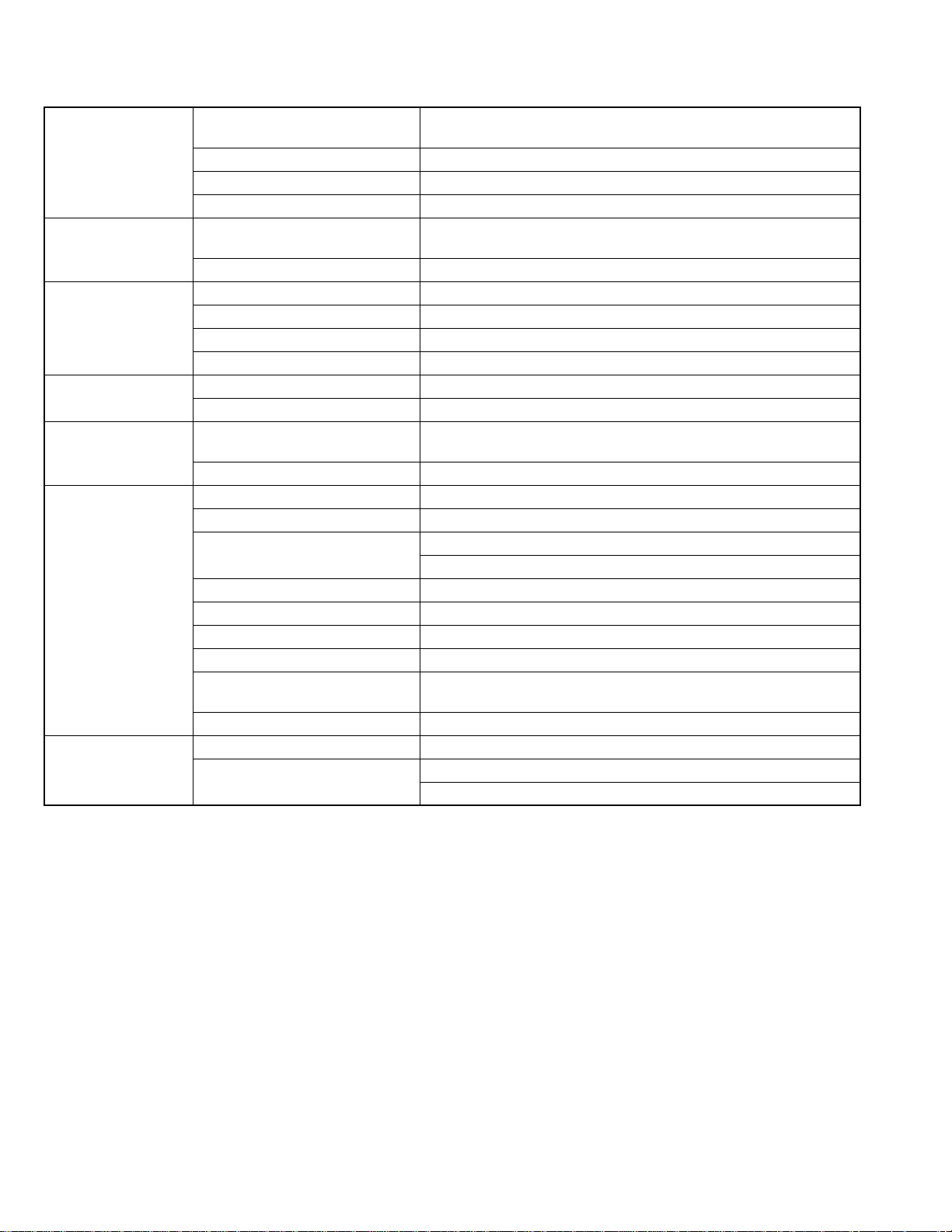
(5) Leakage shock hazard testing
After reassembling the product, always perform an isolation check on the exposed metal parts of the product (antenna terminals, knobs, metal cabinet, screw heads,
headphone jack, control shafts, etc.) to be sure the product
is safe to operate without danger of electrical shock.Do not
use a line isolation transformer during this check.
• Pl ug the AC line cord directly into the AC outlet. Using a
"Leakage Current Tester", measure the leakage current
from each exposed metal parts of the cabinet, particularly any exposed metal part having a return path to the
chassis, to a known good earth ground. Any leakage current must not exceed 0.5mA AC (r.m.s.).
• Alternate check method
Plug the AC line cord directly into the AC outlet. Use an
AC voltmeter having, 1,000Ω per volt or more sensitivity
in the following manner. Connect a 1,500Ω 10W resistor
paralleled by a 0.15µF AC-type capacitor between an exposed metal part and a known good earth ground.
Measure the AC voltage across the resistor with the AC
voltmeter.
Move the resistor connection to each exposed metal
part, particularly any exposed metal part having a return
path to the chassis, and measure the AC voltage across
the resistor. Now, reverse the plug in the AC outlet and
repeat each measurement. Voltage measured any must
not exceed 0.75 V AC (r.m.s.). This corresponds to 0.5
mA AC (r.m.s.).
AC VOLTMETER
(Having 1000
ohms/volts,
or more sensitivity)
0.15 F AC TYPE
Place this
probe on
1500 10W
Good earth ground
1.2 Warning
(1) This equipment has been designed and manufactured to
meet international safety standards.
(2) It is the legal resp onsibility of the repairer to ensure that
these safety standards are maintained.
(3) Repairs must be made in accordance with the relevant
safety standards.
(4) It is essential that safety critical compone nts are replaced
by approved parts.
(5) If mains voltage selector is provided, check setting for local
voltage.
1.3 Caution
Burrs formed during molding may be left over on some parts
of the chassis.
Therefore, pay attention to such burrs in the case of preforming repair of this system.
1.4 Critical parts for safety
In regard with component parts appearing on the silk-screen
printed side (parts side) of the PWB diagrams, the parts that are
printed over with black such as the resistor ( ), diode ( )
and ICP ( ) or identified by the " " mark nearby are critical
for safety. When replacing them, be sure to use the parts of the
same type and rating as specified by the manufacturer.
(This regulation dose not Except the J and C version)
each exposed
metal part.
(No.MB157)1-3
Page 4
1.5 Preventing static electricity
Electrostatic discharge (ESD), which occurs when static electricity stored in the body, fabric, etc. is discharged, can destroy the laser
diode in the traverse unit (optical pickup). Take care to prevent this when performing repairs.
1.5.1 Grounding to prevent damage by static electricity
Static electricity in the work area can destroy the optical pickup (laser dio de) in devices such as CD players.
Be careful to use proper grounding in the area where repairs are being performed.
(1) Ground the workbench
Ground the workbench by laying conductive material (such as a conductive sh eet) or an iron plate over it before placing the
traverse unit (optical pickup) on it.
(2) Ground yourself
Use an anti-static wrist strap to release any static electricity built up in your body.
(caption)
Anti-static wrist strap
1M
Conductive material
(conductive sheet) or iron palate
(3) Handling the optical pickup
• In order to maintain quality during transport and before instal lation, both sides of the laser di ode on the replacement optica l
pickup are shorted. After replacement, return the shorted parts to their original condition.
(Refer to the text.)
• Do not use a tester to check the condition of the laser diode in the optical pickup. The tester's internal power source can easily
destroy the laser diode.
1.6 Handling the traverse unit (optical pickup)
(1) Do not subject the traverse unit (optical pickup) to strong shocks, as it is a sensitive, complex unit.
(2) Cut off the shorted part of the flexible cable using nippers, etc. after replacing the optical pickup. For specific details, refer to the
replacement procedure in the text. Remove the anti-static pin when replacing the traverse unit. Be careful not to take too long
a time when attaching it to the connector.
(3) Handle the flexible cable carefully as it may break when subjected to strong force.
(4) I t is not possible to adjust the semi-fixed resistor that adjusts the laser power. Do not turn it.
1.7 Attention when traverse unit is decomposed
*Please refer to "Disassembly method" in the text for the CD pickup unit.
• Apply solder to the short land sections before the flexible wir e is disconnected from the connector on the CD servo board. (If the
flexible wire is disconnected without applying solder, the CD pickup may be destroyed by static electricity.)
• In the assembly, be sure to remove solder from the short land sections after connecting the flexible wire.
CD changer
unit
1-4 (No.MB157)
Flexible cable
Soldering
Page 5

1.8 Importance administering point on the safety
Caution: For continued protection against risk of
fire, replace only with same type 3.15A/250V for
F951 and 1.6A/250V for F952. This symbol
specifies type of fast operating fuse.
Precaution: Pour eviter risques de feux, remplacez
le fusible de surete de F951 comme le meme type
que 3.15A/250V, et 1.6A/250V pour F952.
Ce sont des fusibles suretes qui functionnes rapide.
^
(No.MB157)1-5
Page 6

SECTION 2
SPECIFIC SERVICE INSTRUCTIONS
This service manual does not describe SPECIFIC SERVICE INSTRUCTIONS.
1-6 (No.MB157)
Page 7
SECTION 3
DISASSEMBLY
3.1 Main body
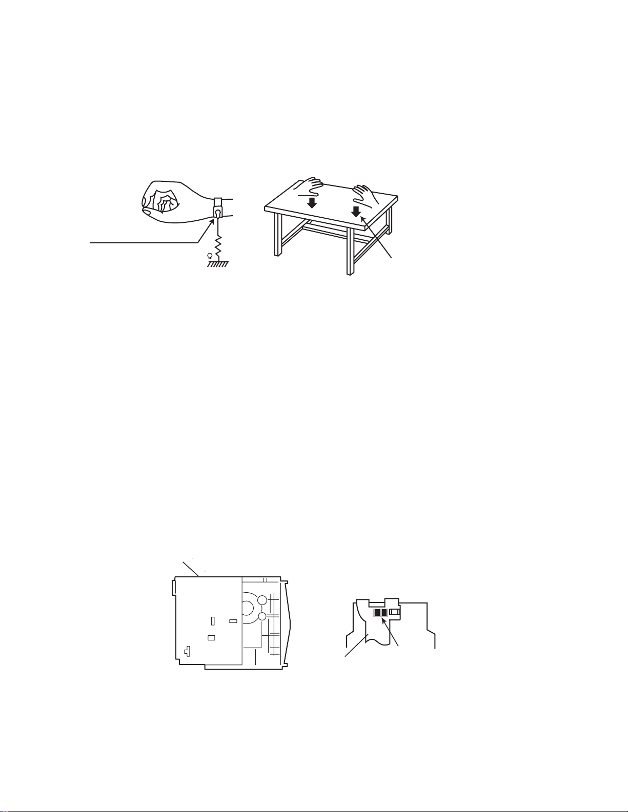
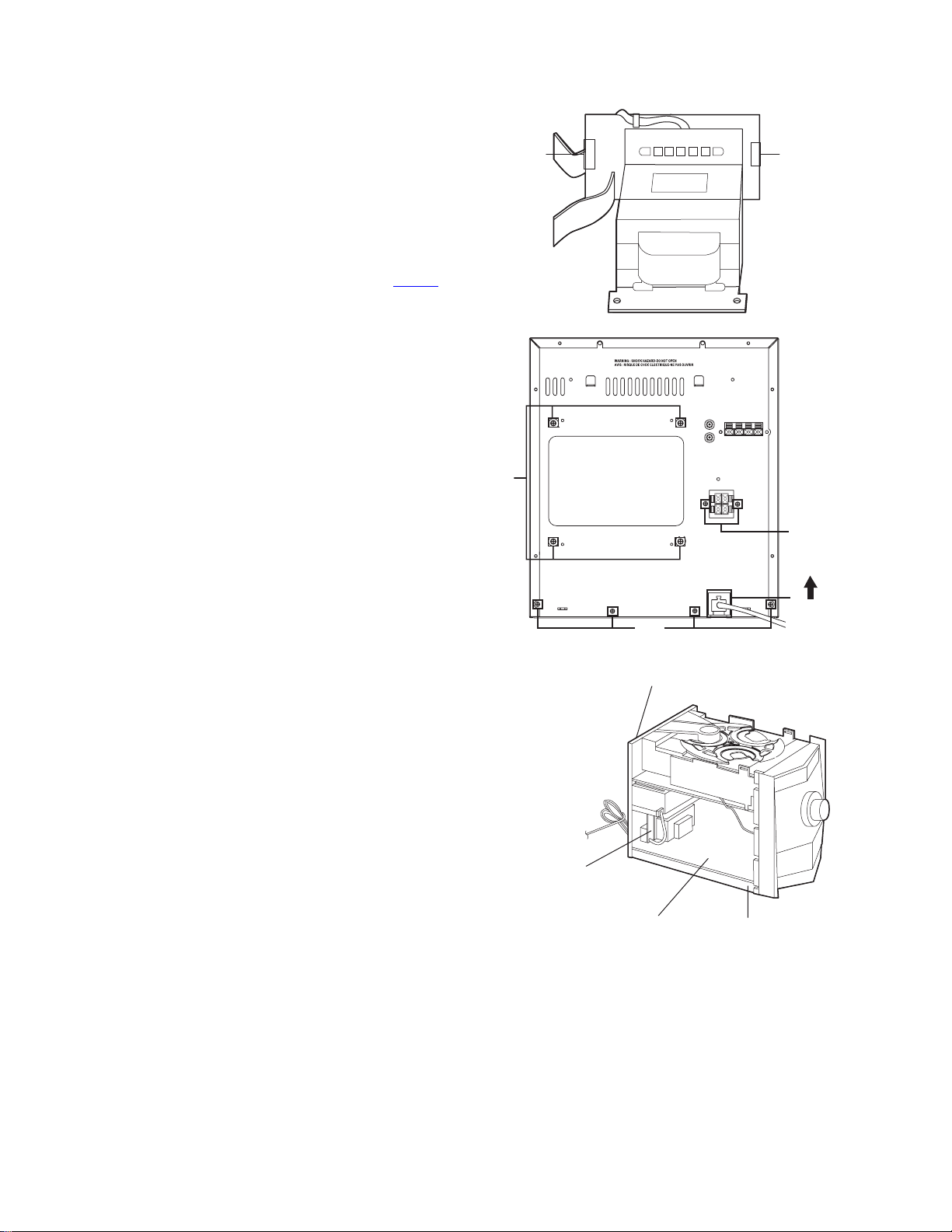
3.1.1 Replacing the fuses
(See Fig.1)
• Prio r to performing the following procedure, remove the top
cover.
(1) Replace the fuse s inside.
Caution:
Be sure to use fuses with the specified ratings.
3.1.2 Replacing the power IC
(See Fig.2)
• Prio r to performing the following procedure, remove the top
cover.
(1) Remove the two screws A from the heat sink between the
power IC.
(2) Remove the solder fixing the power IC.
Fuse(F952)
1.6A 250V
Fuse(F951)
3.15A 250V
Fig.1
A
3.1.3 Replacing the heat sink cover
(See Fig.3)
(1) Remove four screws B from the rear panel.
(2) Pull the heat sink cover outward.
Fig.2
B
Fig.3
(No.MB157)1-7
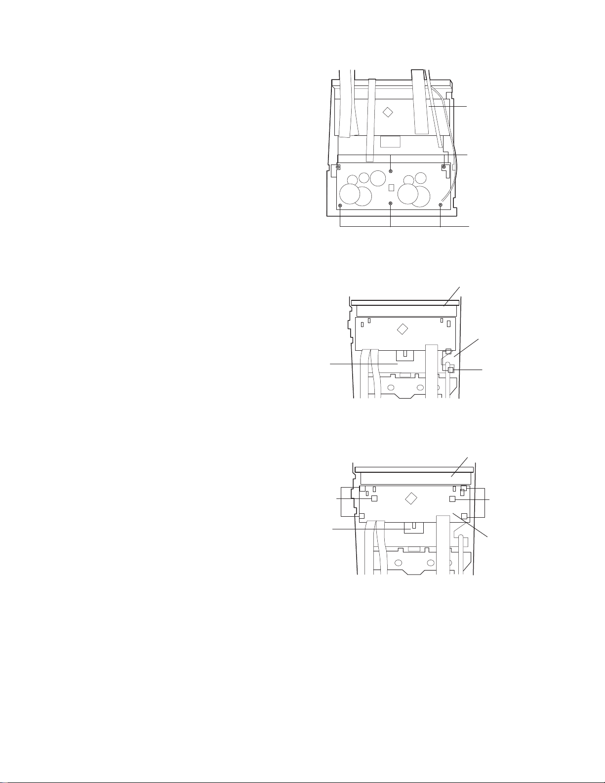
Page 8
3.1.4 Removing the top cover
(See Fig.4 and 5)
(1) Remove six screws C that retain the top cover from the
panel rear of the body.
(2) Remove six screws D that retain the top cover from the two
sides of the body.
(3) Remove the top cover from the body by lifting it toward the
rear.
Top cover
C
C
Fig.4
Right Front panel assembly
Left Front panel assembly
D
C
D
DD
Fig.5
1-8 (No.MB157)
Page 9
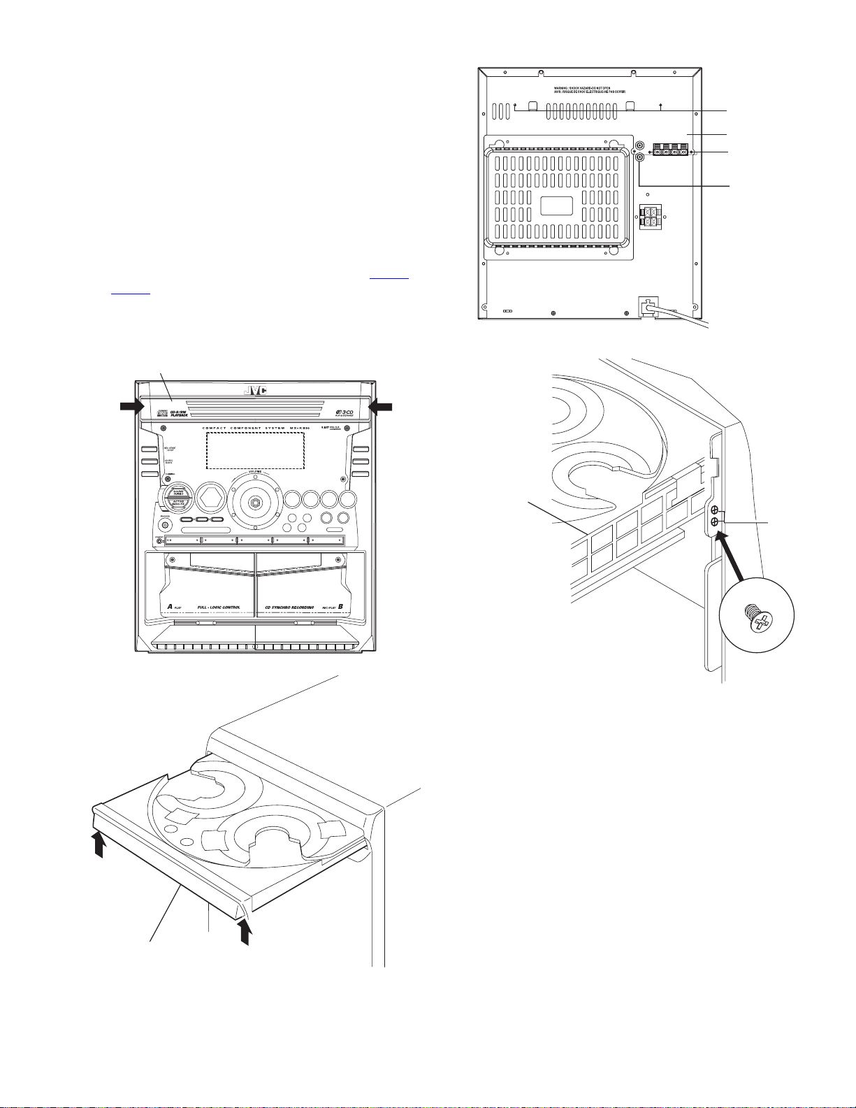
3.1.5 Removing the CD changer unit
y
(See Fig.6 to 9)
• Prio r to performing the following procedures, remove the top
cover.
Caution:
Although the CD mechanism unit can be removed without
removing the CD tray panel, it is still recommended to remove
it in order to prevent damage.
• From the fron t panel side of this set, push in the sections
marked with arrows and pull out the CD tray toward the front.
• Remove the CD tray panel by pushing both of its extremities
upward in the direction of the arrows.
• Push the CD tray deep into the set.
(1) Disconnect the cord wires from the CD board CN703
and
CN203.
(2) From the rear of the set, remove two screws E three screws
F and four screws G on the front panel left and right side.
(3) Handle the CD changer unit rear, take out the unit.
CD tray panel
E
Antenna
terminal
F
Accessor
terminal
Fig.8
Fig.6
CD changer
unit
G
Fig.9
CD tray panel
Fig.7
(No.MB157)1-9
Page 10
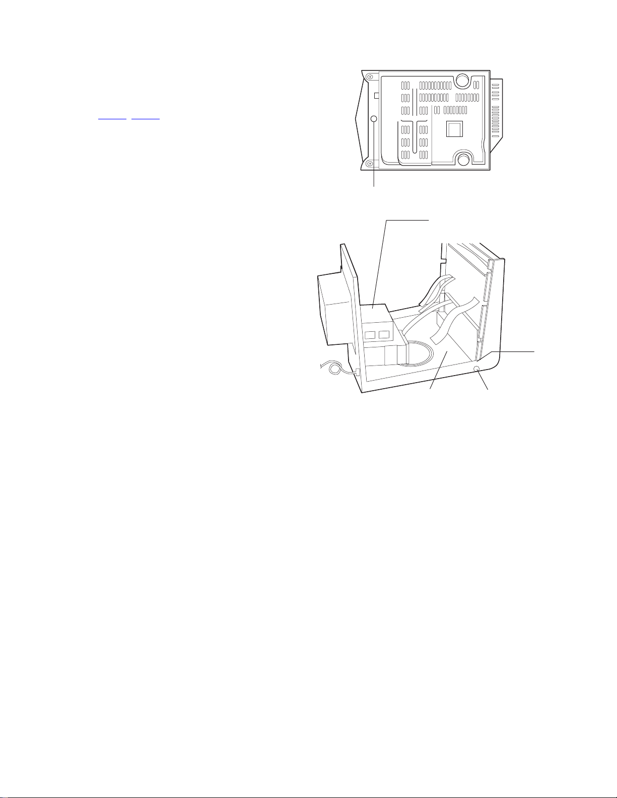
3.1.6 Removing the front panel assembly
(See Fig.10 to 11)
• Prior to performing the following procedures, remove the top
cover.
• Also remove the CD changer unit.
(1) Disconnect the parallel wire and the cord wire from the
connectors CN701
(2) Remove one screws H retaining the front panel assembly
onto the bottom of the body.
(3) Remove two screws I on the left and right side of the set
retaining the panel front from the bottom and then remove
then GND lug b that comes from the power amp and supply
PCB.
(4) Disengage the claws c on both sides of the front panel
assembly and then remove the assembly.
, CN101 on the power amp. board.
*
Fig.10
Power amp and
supply PCB
GND lug b
Fig.11
I
Claw c
1-10 (No.MB157)
Page 11

3.1.7 Removing the CD board
(See Fig.12 to 13)
• Prio r to performing the following procedures, remove the top
cover.
• Also remove the CD changer unit.
(1) Disconnect the wires from CN603A
on the CD board, which is located on the back side of the
CD changer unit.
(2) The four screws J that retain the CD board should be
removed.
(3) Remove the CD board by pulling it toward the side where
the CN601
(4) Using solder, short the CD pickup to connect to short
round.
Caution:
After re-connecting the wires, be sure to remove the
shorting solder from the GND connection.
(5) Disconnect the card wire from the connector CN601
main board and then remove the main board.
is located.
, CN603B and CN604
on the
CD PCB
J
J
J
Fig.12
CD PCB
CN601
Short round
Fig.13
(No.MB157)1-11
Page 12
3.1.8 Removing the CD changer mechanism assembly
(See Fig.14 to 15)
• Prior to performing the following procedures, remove the top
cover.
• Also remove the CD changer unit.
(1) Turn the CD changer mech anism cover base an d remove
the screws d connecting the unit to the CD changer
mechanism assembly.
(2) Removing four screws e retaining the CD mechanism
holder assembly.
Caution:
When replacing the CD changer mechanism assembly, be
sure not to mistake the positions of the silver color and copper
color spring.
CD changer
unit
CD changer
mechanism
assembly
Fig.14
e (Silver color)
e (Silver color)
Fig.15
d
e (copper color)
e (copper color)
1-12 (No.MB157)
Page 13

3.1.9 Removing the CD pickup
r
(See Fig.16)
• Prio r to performing the following procedures, remove the top
cover.
• Also remove the CD changer unit.
• Also remove the CD changer mechanism.
(1) Widen the section f.
(2) While keeping the section f wide open, pu sh the sectio n g
in the direction of the arrow to remove the shaft, and th en
remove the CD pickup.
CD pic kup
f
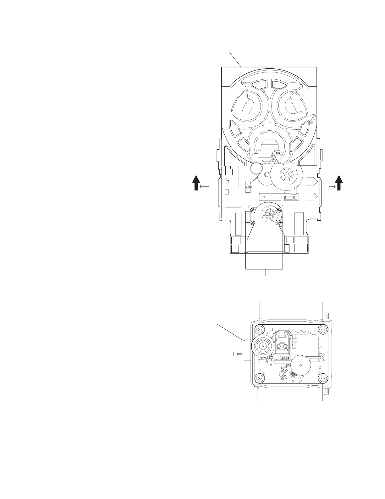
3.1.10 Replacing the loading motor and rotor belt of the CD changer
(See Fig .17)
• Prio r to performing the following procedures, remove the top
cover.
• Al so open the CD changer tray.
(1) Remove the two screws L retaining the CD cha nger tray
loading motor.
(2) Remove the two screws M retaining the gear plate and take
it out, after remove the rotor belt from the pulley.
3.1.11 Replacing the CD turn table and removing the motor
(See Fig. 18)
• Prio r to performing the following procedures, remove the top
cover.
• Also remove the CD changer unit.
(1) Remove the one screws N retaining the CD (Turn table).
(2) Remove the two screws O retaining the sto pper brackets
on both sides of the CD changer unit.
(3) Remove the stopper brackets from both sides of the CD
changer unit.
(4) Pull out the CD tray from the CD chang er unit, all the way
and lift the tray (u/~ ward) to remove.
(5) Remove the gear and after push out the tray motor locker
and pull out the tray motor from the CD tray.
g
Shaft
Fig.16
M
L
Fig.17
Turn table motor
Motor locker
Obligue gea
Fig.18
(No.MB157)1-13
Page 14
3.1.12 Removing the cassette deck mechanism
(See Fig.19)
• Prior to performing the following procedures, remove the top
cover.
• Also remove the CD changer unit.
• Also remove the front panel assembly.
(1) Remove six screws Z retaining the cassette deck
mechanism.
3.1.13 Removing the earphone jack board
(See Fig.20)
• Prior to performing the following procedures, remove the top
cover.
• Also remove the CD changer unit.
• Also remove the front panel assembly.
(1) Remove the screw with the washer, P that retains the
earphone jack PCB.
KEY 1
PCB
Front panel
assembly
Z
Z
Fig.19
Front panel
assembly
Earphone jack
PCB
P
3.1.14 Removing the control/FL board
(See Fig.21)
• Prior to performing the following procedures, remove the top
cover.
• Also remove the CD changer unit.
• Also remove the front panel assembly.
(1) Remove six screws Q that retain the control/FL PCB from
the back of the front panel unit.
Q
KEY 2
PCB
Fig.20
Front panel
assembly
Q
Control/FL
PCB
Fig.21
1-14 (No.MB157)
Page 15
3.1.15 Removing the switch board and sound mode and CD function switch board
y
(See Fig.20 to 23)
• Prio r to performing the following procedures, remove the top
cover.
• Also remove the CD changer unit.
• Also remove the front panel assembly.
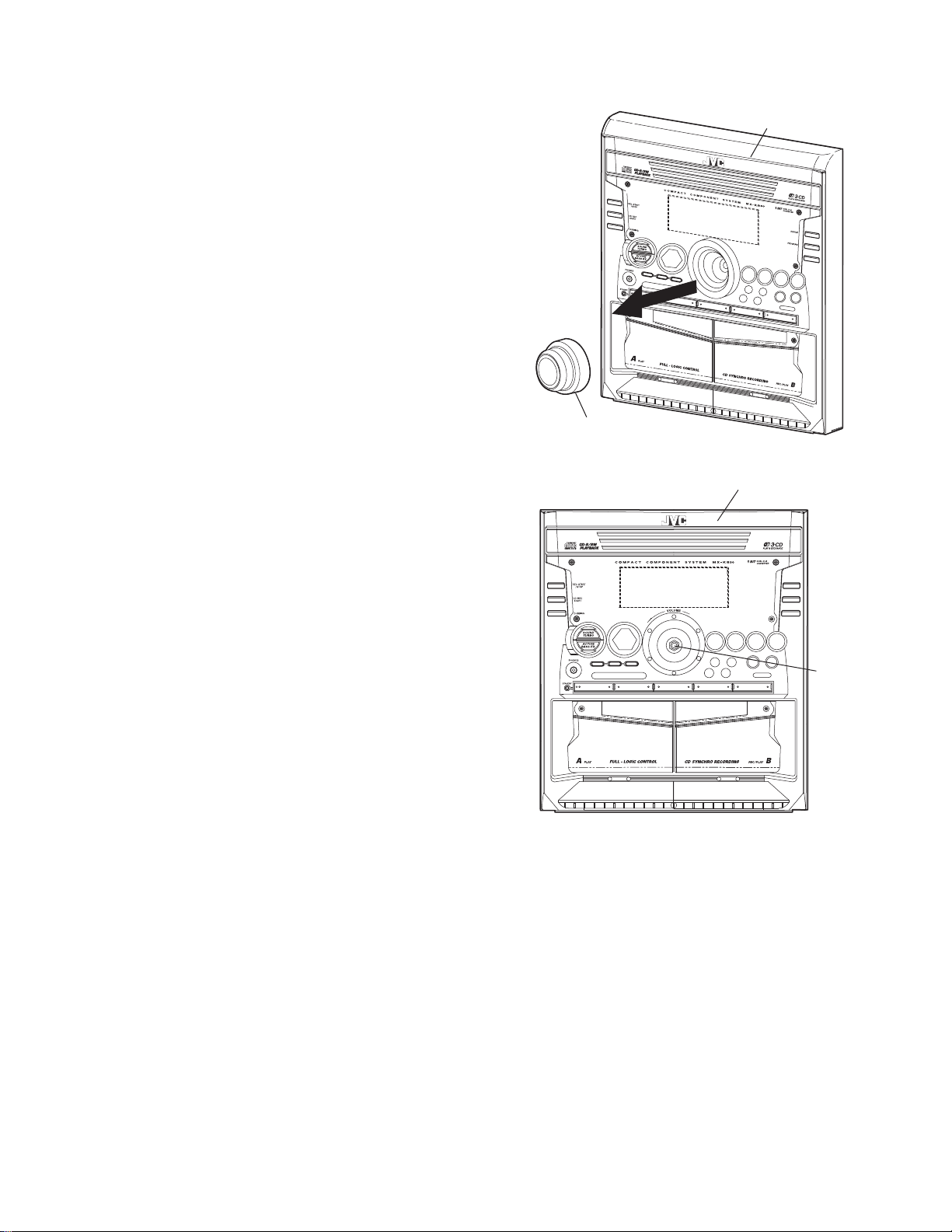
(1) Pull out the volume control knob from the front of the front
panel assembly.(Fig.22)
(2) Remove six screws Q retaining the front panel
assembly.(Fig.21)
(3) Remove the control/FL board.
(4) Remove eleven screws R retaining the switch (key 1)
board.(Fig.20)
(5) Remove two screws S retaining the sound mode and CD
function (key 2) switch board.(Fig.21)
Volume Knob
Front panel assembl
Fig.22
Front panel
assembly
Volume
shaft
Fig.23
(No.MB157)1-15
Page 16
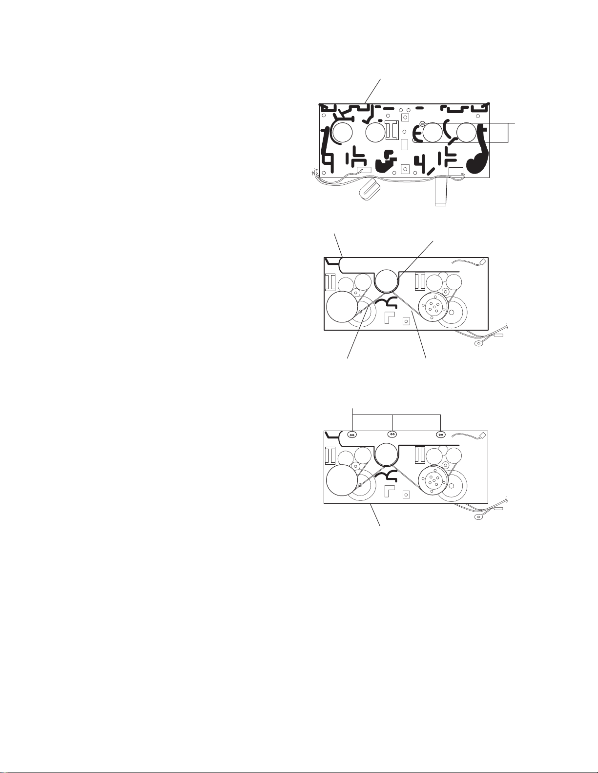
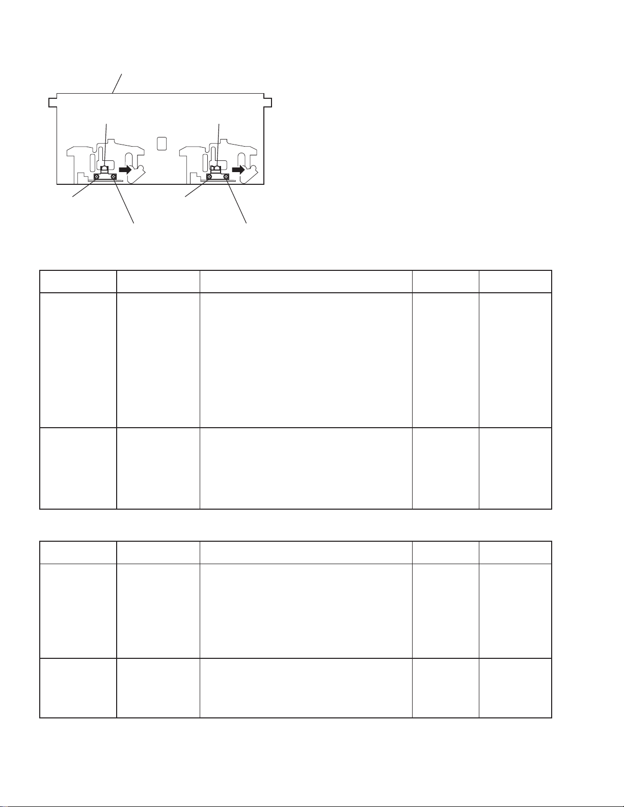
3.1.16 Removing the leaf switches of the cassette deck mechanism
r
(See Fig. 19 and 26)
• Prior to performing the following procedures, remove the top
cover and both sides board.
• Also remove the CD changer unit.
• Also remove the front panel assembly.
(1) Remove the six screws Z that retain the cassette deck
mechanism. (Fig.19)
(2) Remove the cassette deck mechanism.
(3) Turn the cassette deck mechanism upside down.
(4) Remove the solder from around the leaf switches.
(5) Pull out the leaf switches from the front side of the cassette
deck mechanism.
3.1.17 Removing the cassette deck main motor, and
replacing the main belts
(See Fig.19, 24 and 25)
• Prior to performing the following procedures, remove the top
cover and both sides board.
• Also remove the CD changer unit.
• Also remove the front panel assembly.
(1) Remove six screws Z retaining the cassette deck
mechanism. (Fig.19)
(2) Remove the cassette deck mechanism.
(3) Remove two screws t retaining the main motor from the
front side of the cassette deck.
Caution:
After attaching the main motor, check the orientation of
the motor and the polarity of the wires.
(4) From the backside of the cassette deck, remove the main
motor and two main belts.
Caution:
The lengths of the cassette A(playback only) and
cassette B(record/play) main belts are different. When
attaching the main belts, use the longer belt for cassette
A.
Cassette dec k mechanism
Cassette dec k mechanism
(Bac k side)
Main belt
(For B cassete)
Solder side of leaf switch
(Frint side)
t
Fig.24
Casset dec k main moto
Main belt
(For A cassete)
Fig.25
1-16 (No.MB157)
Cassette dec k mechanism
(Bac k side)
Fig.26
Page 17
3.1.18 Removing the cassette deck heads
(See Fig. 19 and 27)
• Prio r to performing the following procedures, remove the top
cover and both sides board.
• Also remove the CD changer unit.
• Also remove the front panel assembly.
(1) Remove six screws Z that retain the cassette deck
mechanism. (Fig.19)
(2) Remove the cassette deck mechanism and place it so that
the front side faces up.
(3) Remove the solder from the bottom side of the head
terminal and disconnect the wire.
(4) Remove screw U that retains the head.
(5) Remove screw V that retains the head.
(6) Hold the head and slide it in the direction of the arrow to
remove it.
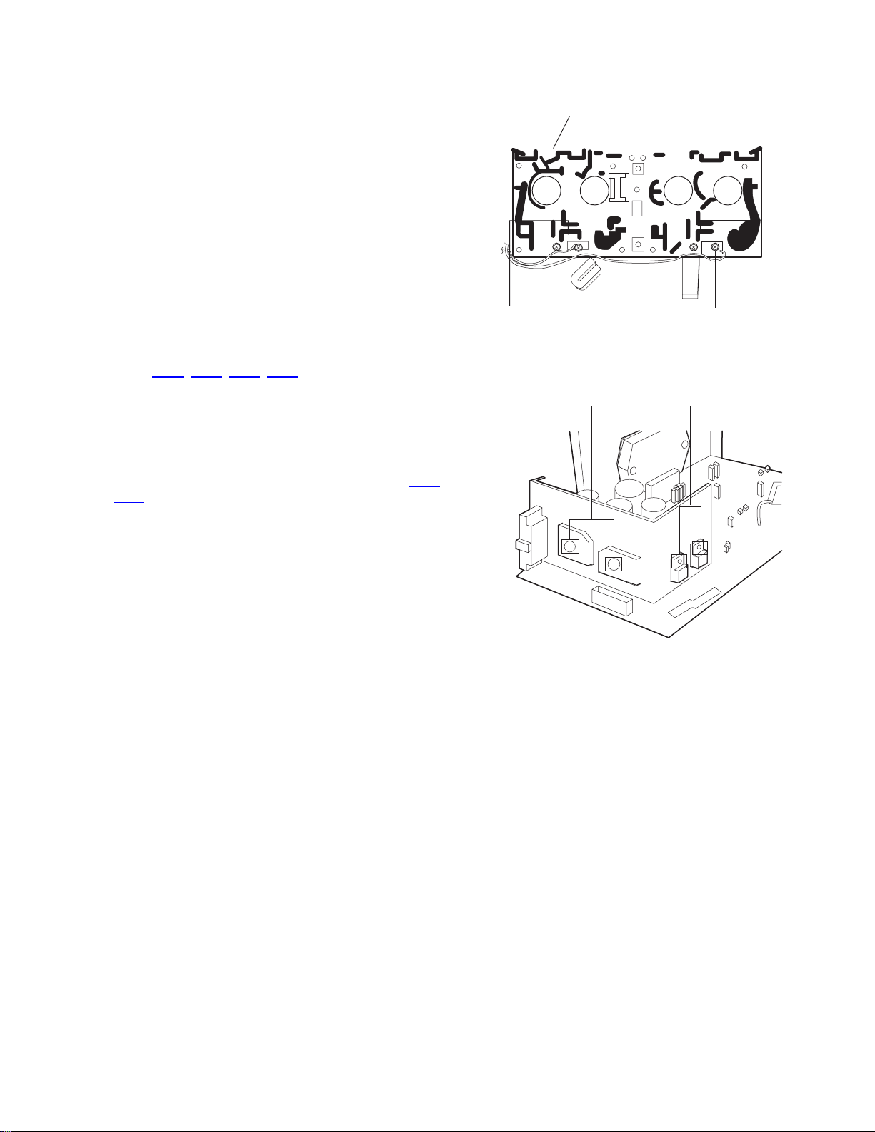
3.1.19 Removing the 3-pin regulator and bridge diode
(See Q904
• Prio r to performing the following procedures, remove the top
cover and both sides board.
(1) Remove two screws A that connect the heat sink.
(2) Remove two screws W that connect the heat sink.
(3) Remove the solder fixing the the 3-pin terminal regulator
Q904
(4) Remove the solder fixing the 4-pin bridge diode (D901,
D914
, Q907, D901, D914 and Fig.28)
, Q907.
).
PB Head
Cassette dec k mechanism
(Front side)
V
U
Fig.27
WA
U
V
REC/PB Head
Fig.28
(No.MB157)1-17
Page 18
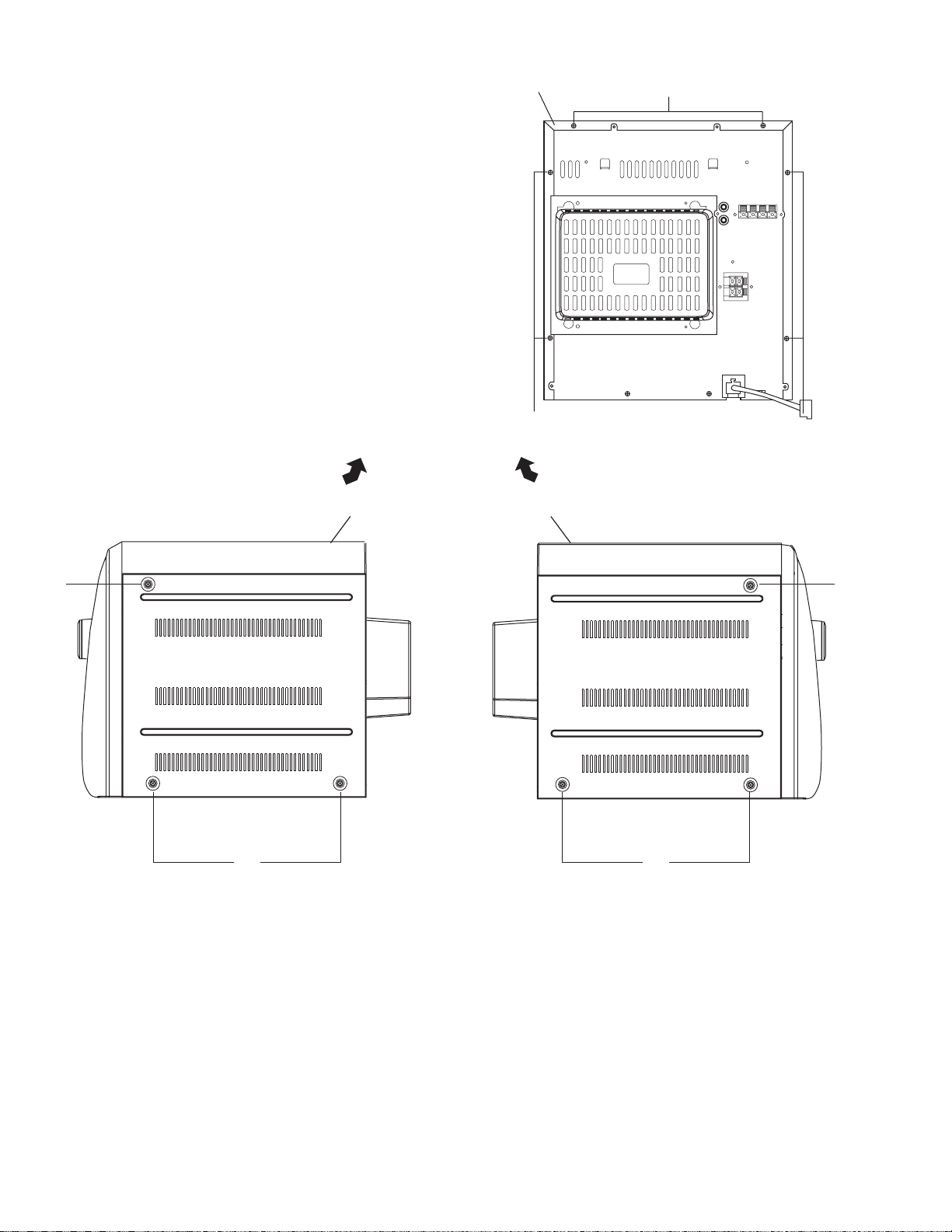
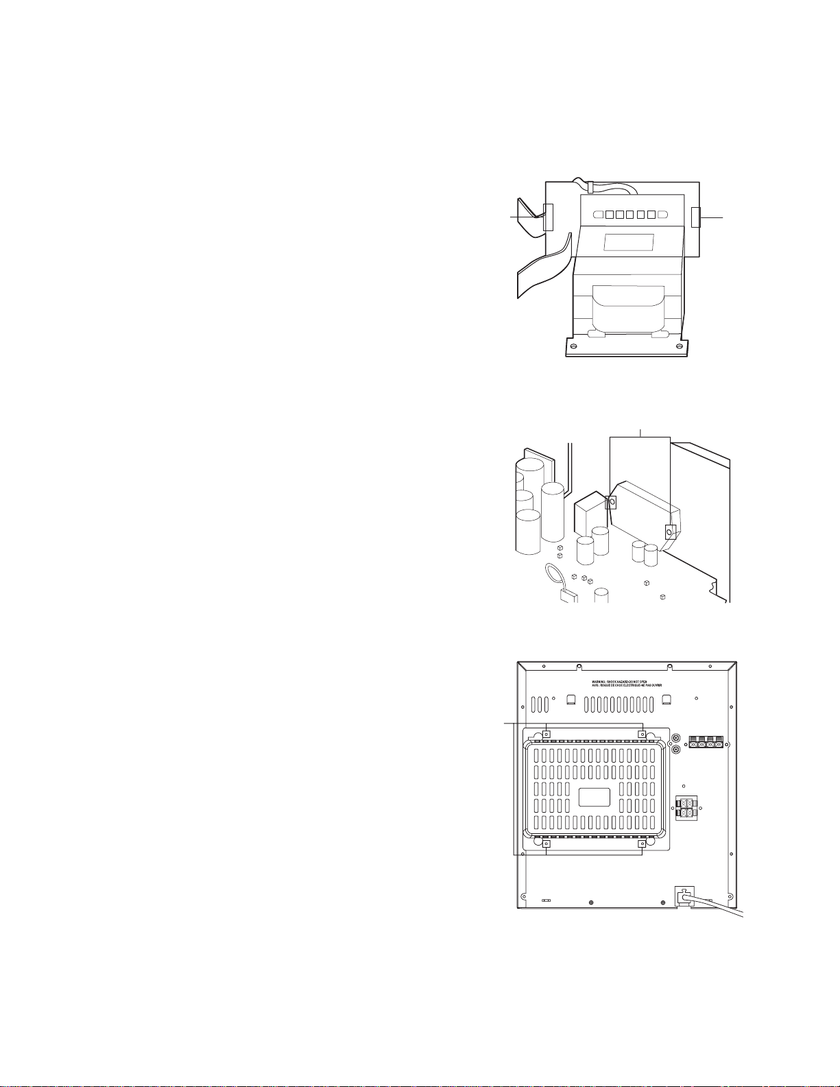
3.1.20 Removing the power amp and supply board and the power trans board
A
(See Fig. 3, 29 to 31)
• Prior to performing the following procedures, remove the top
cover and CD changer unit.
(1) Remove four screws B from the rear panel. (Fig.3)
(2) Pull the heat sink cover outward.
(3) Remove four screws AA from the rear panel between the
heat sink holder.
(4) Remove two screws X that retain the speaker terminals
and AUX terminal.
(5) Remove screws YY that retains the rear panel, and then
remove the rear panel.
(6) Disconnect the parallel wires from the connectors FW951
on the power trans board.
(7) Remove the clamp of AC power cord from the chassis.
(8) Remove four screws AB that retain the pow er trans board
and then remove the assembly.
Fuse(F952)
1.6A 250V
A
Fuse(F951)
3.15A 250V
Fig.29
Power amp and
supply PCB
X
Clamp
YY
Fig.30
Rear panel
AB Chassis
Fig.31
1-18 (No.MB157)
Page 19

SECTION 4
ADJUSTMENT
4.1 Measurement instruments required for adjustment
(1) Low frequency oscillator
This oscillator should have a capacity to output 0dB to
600ohm at an oscillation frequency of 50Hz-20kHz.
(2) Attenuator impedance : 600Ω
(3) Electronic voltmeter
(4) Frequency counter
(5) Wow flutter meter
(6) Test tape
VT712 : For Tape speed and wow flutter ( 3kHz)
VT703 : For Head angle (10kHz)
(7) Blank tape
TAPE I : AC-225
TAPE II : AC-514
(8) Torque gauge
For play and back tension forward : TW2111A
Reverse : TW2121A
Fast Forward and Rewind : TW2231A
(9) Test disc : CTS-1000(12cm),GRG-1211(8cm)
(10) Jitter meter
4.2 Measurement conditions
Power supply voltage : AC 120V (60Hz)
Measurement output terminal
: Speaker out
: TP101(Measuring for TUNER/DECK/CD)
: Dummy load 6Ω
4.3 Radio input signal
AM modulation frequency : 400Hz
Modulation factor : 30%
FM modulation frequency : 1kHz
Frequency displacement : 22.5kHz
4.4 Frequency Range
AM : 530kHz~1710kHz
FM : 87.5MHz~108MHz
4.5 Standard measurement positions of volume and
switch
Power : Standby (Light STANDBY Indicator)
Sound Turbo,A,BASS EX : OFF
Sound mode : OFF
Main VOL. : 0 Minimum
Travers mecha set position : Disc 1
4.6 Precautions for measurement
(1) Apply 30pF and 33k<ohm> to the IF sweeper output side
and 0.082<micro>F and 100kohm in series to the sweeper
input side.
(2) The IF sweeper output level should be made as low as pos-
sible within the adjustable range.
(3) Since the IF sweep er is a fixed device, there is no need to
adjust this sweeper.
(4) Since a ceramic oscillator is used, there is no need to per-
form any MPX adjustment.
(5) Since a fixed coil is used, there is no need to adjust the FM
tracking.
(6) The input and output earth systems are separated.
In case of simultaneously measuring the voltage in both of
the input and output systems with anelectronic voltmeter
for two channels, therefore, the earth should be connected
particularly.
(7) In the case of BTL connection amplifier, the minus terminal
of speaker is not for earthing. Therefore, be sure not to connect any other earth terminal to this terminal. This system
is of an OTL system.
(No.MB157)1-19
Page 20
4.7 Arrangement of adjusting positions
Cassette deck mechanism
(Front side)
PB Head
k-A)
(Dec
Head azimuth screw
(Forward side)
Head azimuth screw
erse side)
(Rev
4.8 Tape recorder section
Items
Cassette Head
Azimuth Alignments
Measurement
conditions
Test tape
: VT703 (10kHz)
Measurement output
terminal
: Left and Right
speaker output
(6-ohm loaded)
or
Headphone Output
(32-ohm loaded)
REC/PB Head
(Deck-B)
Head azimuth screw
(Forw
ard side)
Head azimuth screw
1. Playback the test tape VT703 (10KHz) or equivalent.
2. Adjust the head azimuth screw to obtain maximum
3. Put on the screw lock paint after alignments.
(Reverse side)
Measurement method
output and both output of L / R is in 3dB.
Standard
values
Maximum output
Adjusting
positions
Adjust the
head azimuth
screw only
when the head
has been
changed.
Recording Bias
F
requency Alignment
Test tape
: TYPE I AC-514
Measurement output
terminal
1. Insert the recording tape in deck-B.
2. Starting the recording.
3. Adjust the oscillation frequency to 80KHz+/-3KHz by
core of Oscillation coil of L301.
: Erase head terminal
(CN308 8-Pin)
4.9 Tuner section
Items
AM Tracking
Alignments
Measurement
conditions
Input signal
: 530kHz
600kHz
Adjustment point
: Antenna coil (L2)
1. Set the Signal Generator signal to 530KHz the feed
to Loop Antenna.
2. Receiving the signal and the adjust the OSC coil (L2)
obtain the V.T is 1.40V +/-0.05V.
3. Change the receiving frequency to 600KHz (603KHz).
4. Adjust the Antenna coil ( L2 ) obtain maximum
sensitivity. (Adjust the SSG output to out of AGC range.)
AM IFT Alignments
Input signal
: 530kHz
Adjustment point
: IFT (T1)
1. Set the receiving frequency to 530KHz.
2. Feed the 450KHz signal to AM antenna input.
3.Adjust the IFT Block T1 obtain to maximum output.
(Adjust the SSG output to out of AGC range.)
Note: The adjustment of CD section is not required.
Measurement method
80kHz+/-3kHz
Standard
values
V. T
: 1.40V+/-0.05V
Maximum
sensitivity
Maximum output
Use the HighImpedance
Probe or
Frequency
counter input.
Adjusting
positions
Adjust the OSC
coil only when
the AM coil block
has been changed.
Adjust the IFT
only when the
IFT block has
been changed.
1-20 (No.MB157)
Page 21

SECTION 5
TROUBLESHOOTING
This service manual does not describe TROUBLESHOOTING.
(No.MB157)1-21
Page 22

1-22 (No.MB157)
Page 23

VICTOR COMPANY OF JAPAN, LIMITED
AV & MULTIMEDIA COMPANY AUDIO/VIDEO SYSTEMS CATEGORY 10-1,1chome,Ohwatari-machi,Maebashi-city,371-8543,Japan
(No.MB157)
Printed in Japan
WPC
Page 24
SERVICE MANUAL
COMPACT COMPONENT SYSTEM
MB15720042
MX-KB30
STANDBY/ON
SLEEP
AUX
FM MODE
FM /AM
CD
CD1CD2CD
3
PROGRAM/RANDOM
REPEAT
TAPE
TAPE
A/B
SOUND
VOLUME
MODE
FADE
ACTIVE
SOUND
MUTING
BASS EX.
TURBO
CA-MXKB30SP-MXKB30 SP-MXKB30
Area Suffix
J ------------------- U.S.A.
C ----------------- Canada
TABLE OF CONTENTS
1 PRECAUTION. . . . . . . . . . . . . . . . . . . . . . . . . . . . . . . . . . . . . . . . . . . . . . . . . . . . . . . . . . . . . . . . . . . . . . . . . 1-3
2 SPECIFIC SERVICE INSTRUCTIONS. . . . . . . . . . . . . . . . . . . . . . . . . . . . . . . . . . . . . . . . . . . . . . . . . . . . . . 1-6
3 DISASSEMBLY . . . . . . . . . . . . . . . . . . . . . . . . . . . . . . . . . . . . . . . . . . . . . . . . . . . . . . . . . . . . . . . . . . . . . . . 1-7
4 ADJUSTMENT . . . . . . . . . . . . . . . . . . . . . . . . . . . . . . . . . . . . . . . . . . . . . . . . . . . . . . . . . . . . . . . . . . . . . . . 1-19
5 TROUBLESHOOTING . . . . . . . . . . . . . . . . . . . . . . . . . . . . . . . . . . . . . . . . . . . . . . . . . . . . . . . . . . . . . . . . . 1-21
COPYRIGHT © 2004 VICTOR COMPANY OF JAPAN, LIMITED
No.MB157
2004/2
Page 25

SPECIFICATION
Amplifier Output Power 150 W per channel, min. RMS, driven into 6 Ω at 1kHz, with no more
than 10% total harmonic distortion
Input Sensitivity/Impedance (1 kHz) AUX IN : 300 mV/50 kΩ
Speaker terminals 6 - 16 Ω
Phones 32 Ω - 1 kΩ
Cassette Deck Frequency Response
Type I (NORMAL)
Wow And Flutter 0.15% (WRMS)
CD Player CD Capacity 3 CDs
Dynamic Range 85 dB
Signal-To-Noise Ratio 85 dB
Wow And Flutter Unmeasurable
Tuner FM Tuner Tuning Range : 87.5 MHz - 108.0 MHz
AM Tuner Tuning Range : 530 kHz - 1 710 kHz
Unit Dimensions 267 mm × 305 mm × 433 mm (W/H/D)
Mass Approx. 8.7 kg (19.2 lbs)
Speaker Specifications
(each unit)
Power Specifications Power Requirements AC 120 V , 60 Hz
SP-MXKB30 3-way bass-reflex type
Type Woofer: 16 cm (6-5/16") cone × 1
Speaker Unit Mid: 5cm (2") cone × 1
Power Handling Capacity 150 W
Impedance 6 Ω
Frequency Range 45 Hz - 22,000 Hz
Sound pressure level 87 dB/W
Dimensions 244 mm × 321 mm × 258 mm (W/H/D)
Mass Approx. 3.6 kg (8.0 lbs)
Power Consumption 135 W (power on mode)
15 mW/ch output into 32 Ω
63 Hz - 12 500 Hz
(10-9/16" × 12-1/16" × 17-1/16")
Tweeter: 2 cm (13/16") dome × 1
·m
(9-5/8" × 12-11/16" × 10-3/16")
18 W (in Standby mode)
Design and specifications are subject to change without notice.
1-2 (No.MB157)
Page 26

SECTION 1
PRECAUTION
1.1 Safety Precautions
(1) This design of th is product contains special hardw are and
many circuits and components specially for safety purposes. For continued protection, no changes should be made
to the original design unless authorized in writing by the
manufacturer. Replacement parts must be identical to
those used in the original circuits. Services should be performed by qualified personnel only.
(2) Alterations of the design or circuitry of the product should
not be made. Any design alterations of the product should
not be made. Any design alterations or additions will void
the manufacturers warranty and will further relieve the
manufacture of responsibility for personal injury or property
damage resulting therefrom.
(3) Many electrical and mechanical parts in the products have
special safety-related characteristics. These characteristics are often not evident from visual inspection nor can the
protection afforded by them necessarily be obtained by using replacement components rated for higher voltage, wattage, etc. Replacement parts which have these special
safety characteristics are identified in the Parts List of Service Manual. Electrical components having such features
are identified by shading on the schematics and by ( ) on
the Parts List in the Service Manual. The use of a substitute
replacement which does not have the same safety characteristics as the recommended replacement parts shown in
the Parts List of Service Manual may create shock, fire, or
other hazards.
(4) The leads in the products are routed and dressed with ties,
clamps, tubings, barriers and the like to be separated from
live parts, high temperature parts, moving parts and/or
sharp edges for the prevention of electric shock and fire
hazard. When service is required, the original lead routing
and dress should be observed, and it should be confirmed
that they have been returned to normal, after reassembling.
(5) Leakage shock hazard testing
After reassembling the product, always perform an isolation check on the exposed metal parts of the product (antenna terminals, knobs, metal cabinet, screw heads,
headphone jack, control shafts, etc.) to be sure the product
is safe to operate without danger of electrical shock.Do not
use a line isolation transformer during this check.
• Pl ug the AC line cord directly into the AC outlet. Using a
"Leakage Current Tester", measure the leakage current
from each exposed metal parts of the cabinet, particularly any exposed metal part having a return path to the
chassis, to a known good earth ground. Any leakage current must not exceed 0.5mA AC (r.m.s.).
• Alternate check method
Plug the AC line cord directly into the AC outlet. Use an
AC voltmeter having, 1,000Ω per volt or more sensitivity
in the following manner. Connect a 1,500Ω 10W resistor
paralleled by a 0.15µF AC-type capacitor between an exposed metal part and a known good earth ground.
Measure the AC voltage across the resistor with the AC
voltmeter.
Move the resistor connection to each exposed metal
part, particularly any exposed metal part having a return
path to the chassis, and measure the AC voltage across
the resistor. Now, reverse the plug in the AC outlet and
repeat each measurement. Voltage measured any must
not exceed 0.75 V AC (r.m.s.). This corresponds to 0.5
mA AC (r.m.s.).
AC VOLTMETER
(Having 1000
ohms/volts,
or more sensitivity)
0.15 F AC TYPE
Place this
probe on
1500 10W
Good earth ground
1.2 Warning
(1) This equipment has been designed and manufactured to
meet international safety standards.
(2) It is the legal resp onsibility of the repairer to ensure that
these safety standards are maintained.
(3) Repairs must be made in accordance with the relevant
safety standards.
(4) It is essential that safety critical compone nts are replaced
by approved parts.
(5) If mains voltage selector is provided, check setting for local
voltage.
1.3 Caution
Burrs formed during molding may be left over on some parts
of the chassis.
Therefore, pay attention to such burrs in the case of preforming repair of this system.
1.4 Critical parts for safety
In regard with component parts appearing on the silk-screen
printed side (parts side) of the PWB diagrams, the parts that are
printed over with black such as the resistor ( ), diode ( )
and ICP ( ) or identified by the " " mark nearby a re critical
for safety. When replacing them, be sure to use the parts of the
same type and rating as specified by the manufacturer.
(This regulation dose not Except the J and C version)
each exposed
metal part.
(No.MB157)1-3
Page 27

1.5 Preventing static electricity
Electrostatic discharge (ESD), which occurs when static electricity stored in the body, fabric, etc. is discharged, can destroy the laser
diode in the traverse unit (optical pickup). Take care to prevent this when performing repairs.
1.5.1 Grounding to prevent damage by static electricity
Static electricity in the work area can destroy the optical pickup (laser dio de) in devices such as CD players.
Be careful to use proper grounding in the area where repairs are being performed.
(1) Ground the workbench
Ground the workbench by laying conductive material (such as a conductive sh eet) or an iron plate over it before placing the
traverse unit (optical pickup) on it.
(2) Ground yourself
Use an anti-static wrist strap to release any static electricity built up in your body.
(caption)
Anti-static wrist strap
1M
Conductive material
(conductive sheet) or iron palate
(3) Handling the optical pickup
• In order to maintain quality during transport and before instal lation, both sides of the laser di ode on the replacement optica l
pickup are shorted. After replacement, return the shorted parts to their original condition.
(Refer to the text.)
• Do not use a tester to check the condition of the laser diode in the optical pickup. The tester's internal power source can easily
destroy the laser diode.
1.6 Handling the traverse unit (optical pickup)
(1) Do not subject the traverse unit (optical pickup) to strong shocks, as it is a sensitive, complex unit.
(2) Cut off the shorted part of the flexible cable using nippers, etc. after replacing the optical pickup. For specific details, refer to the
replacement procedure in the text. Remove the anti-static pin when replacing the traverse unit. Be careful not to take too long
a time when attaching it to the connector.
(3) Handle the flexible cable carefully as it may break when subjected to strong force.
(4) I t is not possible to adjust the semi-fixed resistor that adjusts the laser power. Do not turn it.
1.7 Attention when traverse unit is decomposed
*Please refer to "Disassembly method" in the text for the CD pickup unit.
• Apply solder to the short land sections before the flexible wir e is disconnected from the connector on the CD servo board. (If the
flexible wire is disconnected without applying solder, the CD pickup may be destroyed by static electricity.)
• In the assembly, be sure to remove solder from the short land sections after connecting the flexible wire.
CD changer
unit
1-4 (No.MB157)
Flexible cable
Soldering
Page 28
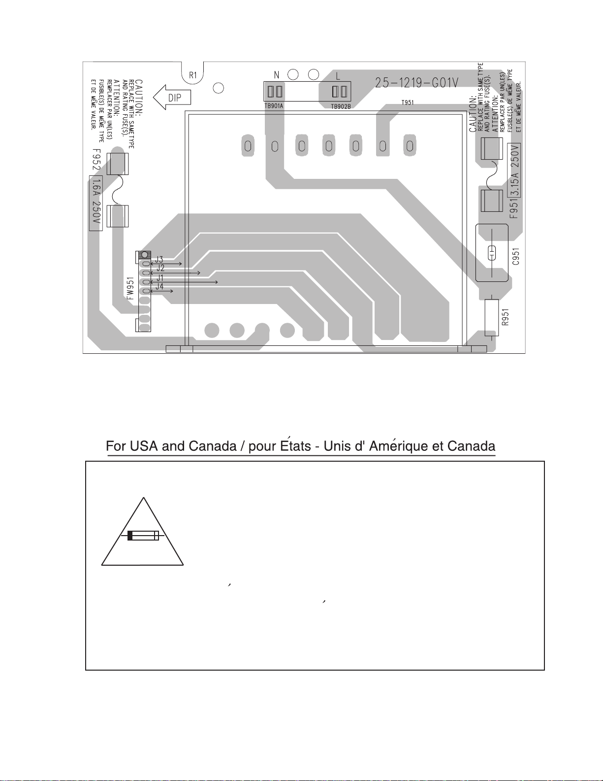
1.8 Importance administering point on the safety
Caution: For continued protection against risk of
fire, replace only with same type 3.15A/250V for
F951 and 1.6A/250V for F952. This symbol
specifies type of fast operating fuse.
Precaution: Pour eviter risques de feux, remplacez
le fusible de surete de F951 comme le meme type
que 3.15A/250V, et 1.6A/250V pour F952.
Ce sont des fusibles suretes qui functionnes rapide.
^
(No.MB157)1-5
Page 29

SECTION 2
SPECIFIC SERVICE INSTRUCTIONS
This service manual does not describe SPECIFIC SERVICE INSTRUCTIONS.
1-6 (No.MB157)
Page 30
SECTION 3
DISASSEMBLY
3.1 Main body
3.1.1 Replacing the fuses
(See Fig.1)
• Prio r to performing the following procedure, remove the top
cover.
(1) Replace the fuse s inside.
Caution:
Be sure to use fuses with the specified ratings.
3.1.2 Replacing the power IC
(See Fig.2)
• Prio r to performing the following procedure, remove the top
cover.
(1) Remove the two screws A from the heat sink between the
power IC.
(2) Remove the solder fixing the power IC.
Fuse(F952)
1.6A 250V
Fuse(F951)
3.15A 250V
Fig.1
A
3.1.3 Replacing the heat sink cover
(See Fig.3)
(1) Remove four screws B from the rear panel.
(2) Pull the heat sink cover outward.
Fig.2
B
Fig.3
(No.MB157)1-7
Page 31

3.1.4 Removing the top cover
(See Fig.4 and 5)
(1) Remove six screws C that retain the top cover from the
panel rear of the body.
(2) Remove six screws D that retain the top cover from the two
sides of the body.
(3) Remove the top cover from the body by lifting it toward the
rear.
Top cover
C
C
Fig.4
Right Front panel assembly
Left Front panel assembly
D
C
D
DD
Fig.5
1-8 (No.MB157)
Page 32

3.1.5 Removing the CD changer unit
y
(See Fig.6 to 9)
• Prio r to performing the following procedures, remove the top
cover.
Caution:
Although the CD mechanism unit can be removed without
removing the CD tray panel, it is still recommended to remove
it in order to prevent damage.
• From the fron t panel side of this set, push in the sections
marked with arrows and pull out the CD tray toward the front.
• Remove the CD tray panel by pushing both of its extremities
upward in the direction of the arrows.
• Push the CD tray deep into the set.
(1) Disconnect the cord wires from the CD board CN703
and
CN203.
(2) From the rear of the set, remove two screws E three screws
F and four screws G on the front panel left and right side.
(3) Handle the CD changer unit rear, take out the unit.
CD tray panel
E
Antenna
terminal
F
Accessor
terminal
Fig.8
Fig.6
CD changer
unit
G
Fig.9
CD tray panel
Fig.7
(No.MB157)1-9
Page 33

3.1.6 Removing the front panel assembly
(See Fig.10 to 11)
• Prior to performing the following procedures, remove the top
cover.
• Also remove the CD changer unit.
(1) Disconnect the parallel wire and the cord wire from the
connectors CN701
(2) Remove one screws H retaining the front panel assembly
onto the bottom of the body.
(3) Remove two screws I on the left and right side of the set
retaining the panel front from the bottom and then remove
then GND lug b that comes from the power amp and supply
PCB.
(4) Disengage the claws c on both sides of the front panel
assembly and then remove the assembly.
, CN101 on the power amp. board.
*
Fig.10
Power amp and
supply PCB
GND lug b
Fig.11
I
Claw c
1-10 (No.MB157)
Page 34

3.1.7 Removing the CD board
(See Fig.12 to 13)
• Prio r to performing the following procedures, remove the top
cover.
• Also remove the CD changer unit.
(1) Disconnect the wires from CN603A
on the CD board, which is located on the back side of the
CD changer unit.
(2) The four screws J that retain the CD board should be
removed.
(3) Remove the CD board by pulling it toward the side where
the CN601
(4) Using solder, short the CD pickup to connect to short
round.
Caution:
After re-connecting the wires, be sure to remove the
shorting solder from the GND connection.
(5) Disconnect the card wire from the connector CN601
main board and then remove the main board.
is located.
, CN603B and CN604
on the
CD PCB
J
J
J
Fig.12
CD PCB
CN601
Short round
Fig.13
(No.MB157)1-11
Page 35

3.1.8 Removing the CD changer mechanism assembly
(See Fig.14 to 15)
• Prior to performing the following procedures, remove the top
cover.
• Also remove the CD changer unit.
(1) Turn the CD changer mech anism cover base an d remove
the screws d connecting the unit to the CD changer
mechanism assembly.
(2) Removing four screws e retaining the CD mechanism
holder assembly.
Caution:
When replacing the CD changer mechanism assembly, be
sure not to mistake the positions of the silver color and copper
color spring.
CD changer
unit
CD changer
mechanism
assembly
Fig.14
e (Silver color)
e (Silver color)
Fig.15
d
e (copper color)
e (copper color)
1-12 (No.MB157)
Page 36

3.1.9 Removing the CD pickup
r
(See Fig.16)
• Prio r to performing the following procedures, remove the top
cover.
• Also remove the CD changer unit.
• Also remove the CD changer mechanism.
(1) Widen the section f.
(2) While keeping the section f wide open, pu sh the sectio n g
in the direction of the arrow to remove the shaft, and th en
remove the CD pickup.
CD pic kup
f
3.1.10 Replacing the loading motor and rotor belt of the CD changer
(See Fig .17)
• Prio r to performing the following procedures, remove the top
cover.
• Al so open the CD changer tray.
(1) Remove the two screws L retaining the CD cha nger tray
loading motor.
(2) Remove the two screws M retaining the gear plate and take
it out, after remove the rotor belt from the pulley.
3.1.11 Replacing the CD turn table and removing the motor
(See Fig. 18)
• Prio r to performing the following procedures, remove the top
cover.
• Also remove the CD changer unit.
(1) Remove the one screws N retaining the CD (Turn table).
(2) Remove the two screws O retaining the sto pper brackets
on both sides of the CD changer unit.
(3) Remove the stopper brackets from both sides of the CD
changer unit.
(4) Pull out the CD tray from the CD chang er unit, all the way
and lift the tray (u/~ ward) to remove.
(5) Remove the gear and after push out the tray motor locker
and pull out the tray motor from the CD tray.
g
Shaft
Fig.16
M
L
Fig.17
Turn table motor
Motor locker
Obligue gea
Fig.18
(No.MB157)1-13
Page 37

3.1.12 Removing the cassette deck mechanism
(See Fig.19)
• Prior to performing the following procedures, remove the top
cover.
• Also remove the CD changer unit.
• Also remove the front panel assembly.
(1) Remove six screws Z retaining the cassette deck
mechanism.
3.1.13 Removing the earphone jack board
(See Fig.20)
• Prior to performing the following procedures, remove the top
cover.
• Also remove the CD changer unit.
• Also remove the front panel assembly.
(1) Remove the screw with the washer, P that retains the
earphone jack PCB.
KEY 1
PCB
Front panel
assembly
Z
Z
Fig.19
Front panel
assembly
Earphone jack
PCB
P
3.1.14 Removing the control/FL board
(See Fig.21)
• Prior to performing the following procedures, remove the top
cover.
• Also remove the CD changer unit.
• Also remove the front panel assembly.
(1) Remove six screws Q that retain the control/FL PCB from
the back of the front panel unit.
Q
KEY 2
PCB
Fig.20
Front panel
assembly
Q
Control/FL
PCB
Fig.21
1-14 (No.MB157)
Page 38

3.1.15 Removing the switch board and sound mode and CD function switch board
y
(See Fig.20 to 23)
• Prio r to performing the following procedures, remove the top
cover.
• Also remove the CD changer unit.
• Also remove the front panel assembly.
(1) Pull out the volume control knob from the front of the front
panel assembly.(Fig.22)
(2) Remove six screws Q retaining the front panel
assembly.(Fig.21)
(3) Remove the control/FL board.
(4) Remove eleven screws R retaining the switch (key 1)
board.(Fig.20)
(5) Remove two screws S retaining the sound mode and CD
function (key 2) switch board.(Fig.21)
Volume Knob
Front panel assembl
Fig.22
Front panel
assembly
Volume
shaft
Fig.23
(No.MB157)1-15
Page 39

3.1.16 Removing the leaf switches of the cassette deck mechanism
r
(See Fig. 19 and 26)
• Prior to performing the following procedures, remove the top
cover and both sides board.
• Also remove the CD changer unit.
• Also remove the front panel assembly.
(1) Remove the six screws Z that retain the cassette deck
mechanism. (Fig.19)
(2) Remove the cassette deck mechanism.
(3) Turn the cassette deck mechanism upside down.
(4) Remove the solder from around the leaf switches.
(5) Pull out the leaf switches from the front side of the cassette
deck mechanism.
3.1.17 Removing the cassette deck main motor, and
replacing the main belts
(See Fig.19, 24 and 25)
• Prior to performing the following procedures, remove the top
cover and both sides board.
• Also remove the CD changer unit.
• Also remove the front panel assembly.
(1) Remove six screws Z retaining the cassette deck
mechanism. (Fig.19)
(2) Remove the cassette deck mechanism.
(3) Remove two screws t retaining the main motor from the
front side of the cassette deck.
Caution:
After attaching the main motor, check the orientation of
the motor and the polarity of the wires.
(4) From the backside of the cassette deck, remove the main
motor and two main belts.
Caution:
The lengths of the cassette A(playback only) and
cassette B(record/play) main belts are different. When
attaching the main belts, use the longer belt for cassette
A.
Cassette dec k mechanism
Cassette dec k mechanism
(Bac k side)
Main belt
(For B cassete)
Solder side of leaf switch
(Frint side)
t
Fig.24
Casset dec k main moto
Main belt
(For A cassete)
Fig.25
1-16 (No.MB157)
Cassette dec k mechanism
(Bac k side)
Fig.26
Page 40

3.1.18 Removing the cassette deck heads
(See Fig. 19 and 27)
• Prio r to performing the following procedures, remove the top
cover and both sides board.
• Also remove the CD changer unit.
• Also remove the front panel assembly.
(1) Remove six screws Z that retain the cassette deck
mechanism. (Fig.19)
(2) Remove the cassette deck mechanism and place it so that
the front side faces up.
(3) Remove the solder from the bottom side of the head
terminal and disconnect the wire.
(4) Remove screw U that retains the head.
(5) Remove screw V that retains the head.
(6) Hold the head and slide it in the direction of the arrow to
remove it.
3.1.19 Removing the 3-pin regulator and bridge diode
(See Q904
• Prio r to performing the following procedures, remove the top
cover and both sides board.
(1) Remove two screws A that connect the heat sink.
(2) Remove two screws W that connect the heat sink.
(3) Remove the solder fixing the the 3-pin terminal regulator
Q904
(4) Remove the solder fixing the 4-pin bridge diode (D901,
D914
, Q907, D901, D914 and Fig.28)
, Q907.
).
PB Head
Cassette dec k mechanism
(Front side)
V
U
Fig.27
WA
U
V
REC/PB Head
Fig.28
(No.MB157)1-17
Page 41

3.1.20 Removing the power amp and supply board and the power trans board
A
(See Fig. 3, 29 to 31)
• Prior to performing the following procedures, remove the top
cover and CD changer unit.
(1) Remove four screws B from the rear panel. (Fig.3)
(2) Pull the heat sink cover outward.
(3) Remove four screws AA from the rear panel between the
heat sink holder.
(4) Remove two screws X that retain the speaker terminals
and AUX terminal.
(5) Remove screws YY that retains the rear panel, and then
remove the rear panel.
(6) Disconnect the parallel wires from the connectors FW951
on the power trans board.
(7) Remove the clamp of AC power cord from the chassis.
(8) Remove four screws AB that retain the pow er trans board
and then remove the assembly.
Fuse(F952)
1.6A 250V
A
Fuse(F951)
3.15A 250V
Fig.29
Power amp and
supply PCB
X
Clamp
YY
Fig.30
Rear panel
AB Chassis
Fig.31
1-18 (No.MB157)
Page 42

SECTION 4
ADJUSTMENT
4.1 Measurement instruments required for adjustment
(1) Low frequency oscillator
This oscillator should have a capacity to output 0dB to
600ohm at an oscillation frequency of 50Hz-20kHz.
(2) Attenuator impedance : 600Ω
(3) Electronic voltmeter
(4) Frequency counter
(5) Wow flutter meter
(6) Test tape
VT712 : For Tape speed and wow flutter ( 3kHz)
VT703 : For Head angle (10kHz)
(7) Blank tape
TAPE I : AC-225
TAPE II : AC-514
(8) Torque gauge
For play and back tension forward : TW2111A
Reverse : TW2121A
Fast Forward and Rewind : TW2231A
(9) Test disc : CTS-1000(12cm),GRG-1211(8cm)
(10) Jitter meter
4.2 Measurement conditions
Power supply voltage : AC 120V (60Hz)
Measurement output terminal
: Speaker out
: TP101(Measuring for TUNER/DECK/CD)
: Dummy load 6Ω
4.3 Radio input signal
AM modulation frequency : 400Hz
Modulation factor : 30%
FM modulation frequency : 1kHz
Frequency displacement : 22.5kHz
4.4 Frequency Range
AM : 530kHz~1710kHz
FM : 87.5MHz~108MHz
4.5 Standard measurement positions of volume and
switch
Power : Standby (Light STANDBY Indicator)
Sound Turbo,A,BASS EX : OFF
Sound mode : OFF
Main VOL. : 0 Minimum
Travers mecha set position : Disc 1
4.6 Precautions for measurement
(1) Apply 30pF and 33k<ohm> to the IF sweeper output side
and 0.082<micro>F and 100kohm in series to the sweeper
input side.
(2) The IF sweeper output level should be made as low as pos-
sible within the adjustable range.
(3) Since the IF sweep er is a fixed device, there is no need to
adjust this sweeper.
(4) Since a ceramic oscillator is used, there is no need to per-
form any MPX adjustment.
(5) Since a fixed coil is used, there is no need to adjust the FM
tracking.
(6) The input and output earth systems are separated.
In case of simultaneously measuring the voltage in both of
the input and output systems with anelectronic voltmeter
for two channels, therefore, the earth should be connected
particularly.
(7) In the case of BTL connection amplifier, the minus terminal
of speaker is not for earthing. Therefore, be sure not to connect any other earth terminal to this terminal. This system
is of an OTL system.
(No.MB157)1-19
Page 43

4.7 Arrangement of adjusting positions
Cassette deck mechanism
(Front side)
PB Head
k-A)
(Dec
Head azimuth screw
(Forward side)
Head azimuth screw
erse side)
(Rev
4.8 Tape recorder section
Items
Cassette Head
Azimuth Alignments
Measurement
conditions
Test tape
: VT703 (10kHz)
Measurement output
terminal
: Left and Right
speaker output
(6-ohm loaded)
or
Headphone Output
(32-ohm loaded)
REC/PB Head
(Deck-B)
Head azimuth screw
(Forw
ard side)
Head azimuth screw
1. Playback the test tape VT703 (10KHz) or equivalent.
2. Adjust the head azimuth screw to obtain maximum
3. Put on the screw lock paint after alignments.
(Reverse side)
Measurement method
output and both output of L / R is in 3dB.
Standard
values
Maximum output
Adjusting
positions
Adjust the
head azimuth
screw only
when the head
has been
changed.
Recording Bias
F
requency Alignment
Test tape
: TYPE I AC-514
Measurement output
terminal
1. Insert the recording tape in deck-B.
2. Starting the recording.
3. Adjust the oscillation frequency to 80KHz+/-3KHz by
core of Oscillation coil of L301.
: Erase head terminal
(CN308 8-Pin)
4.9 Tuner section
Items
AM Tracking
Alignments
Measurement
conditions
Input signal
: 530kHz
600kHz
Adjustment point
: Antenna coil (L2)
1. Set the Signal Generator signal to 530KHz the feed
to Loop Antenna.
2. Receiving the signal and the adjust the OSC coil (L2)
obtain the V.T is 1.40V +/-0.05V.
3. Change the receiving frequency to 600KHz (603KHz).
4. Adjust the Antenna coil ( L2 ) obtain maximum
sensitivity. (Adjust the SSG output to out of AGC range.)
AM IFT Alignments
Input signal
: 530kHz
Adjustment point
: IFT (T1)
1. Set the receiving frequency to 530KHz.
2. Feed the 450KHz signal to AM antenna input.
3.Adjust the IFT Block T1 obtain to maximum output.
(Adjust the SSG output to out of AGC range.)
Note: The adjustment of CD section is not required.
Measurement method
80kHz+/-3kHz
Standard
values
V. T
: 1.40V+/-0.05V
Maximum
sensitivity
Maximum output
Use the HighImpedance
Probe or
Frequency
counter input.
Adjusting
positions
Adjust the OSC
coil only when
the AM coil block
has been changed.
Adjust the IFT
only when the
IFT block has
been changed.
1-20 (No.MB157)
Page 44

SECTION 5
TROUBLESHOOTING
This service manual does not describe TROUBLESHOOTING.
(No.MB157)1-21
Page 45

1-22 (No.MB157)
Page 46

VICTOR COMPANY OF JAPAN, LIMITED
AV & MULTIMEDIA COMPANY AUDIO/VIDEO SYSTEMS CATEGORY 10-1,1chome,Ohwatari-machi,Maebashi-city,371-8543,Japan
(No.MB157)
Printed in Japan
WPC
Page 47

SCHEMATIC DIAGRAMS
COMPACT COMPONENT SYSTEM
MX-KB30
CD-ROM No.SML200402
STANDBY/ON
SLEEP
AUX
FM MODE
FM /AM
CD
CD1CD2CD
3
PROGRAM/RANDOM
REPEAT
TAPE
TAPE
A/B
SOUND
VOLUME
MODE
FADE
ACTIVE
SOUND
MUTING
BASS EX.
TURBO
CA-MXKB30SP-MXKB30 SP-MXKB30
Area Suffix
J ------------------- U.S.A.
C ----------------- Canada
Contents
Block diagram ------------------------------------------------------- 2-1
Standard schematic diagrams ---------------------------------- 2- 2
Printed circuit boards --------------------------------------------- 2- 8
COPYRIGHT 2004 VICTOR COMPANY OF JAPAN, LTD.
No.MB157SCH
2004/2
Page 48

In regard with component parts appearing on the silk-screen printed side (parts side) of
the PWB diagrams, the parts that are printed over with black such as the resistor ( ),
diode ( ) and ICP ( ) or identified by the " " mark nearby are critical for safety.
Page 49

< MEMO >
Page 50

Block diagram
AM/FM
ANT
AUX IN
JA302
IC1
LA1823
AM/FM-MPX
TUNER
IC2
LC72136N
PLL
Deck-A
PB-Head
TO
Deck-B
R/P-Head
TO
Cassette
Mechanism
TO
CD PICKUP
TO
SPINDLE
SLEED
TO
CD MECHA
CN307 JA302CN308CN305CN601CN602CN603
Q303
Bias osc
Q309~Q314
Mechan
Control
AN22000A
CD RF AMP
IC621
BA5936S
IC611
IC401
HA12273F
Tape PB/Rec
Q402,Q502
PB mute
IC402
74HC4094
Q401 REC
mute cont
IC103
TDA7440D
VOL,TONE,
SELECTOR
IC601
MN6627482WA
Digital Servo
Q101
AHB
IC102
BA15215F
Q201
AHB
CN306CN309CN604
TO AMP BOARD
TO FRONT BOARD
CN103
CN707
CN703
TO
AMP CN101
2-1
HEAD PHONE
FW1051
MAAIN BOARD
PHONE JACK
HJ1053
TO
(CN951)
FW951
TO FRONT BOARD
Transformer board
T951
TRANSFORMER
Page 51

TO
Headphone
CN101
Q101
AHB
IC102
BA15215F
Q201
AHB
CN306CN309CN604
TO AMP BOARD
TO FRONT BOARD
TO FRONT BOARD
AMP BOARD
CN103
CN707
CN703
TO
CN306
CN103
VFD
Q203
Mute
Q103
Mute
CN701
TO FRONT
CN701
IC701
MN101C350DFB
MCU
IC301
2CH Power Amp
STK412-030
TO AMP
CN701
CN701
IC702
IR Sensor
F702A
F701A
Speaker
Out
J303
TO
(FW951)
CN951
VOLUME
F702B
JOG KEY'S
F701B
r board
R
AC IN
CN707 CN703
TO MAIN
CN309
TO MAIN
CN604
2-2
Page 52

Standard schematic diagrams
Power transformer section
F952
2-3
Page 53

ams
C951
F952
Parts are safety assurance parts.
When replacing those parts make
sure to use the specified one.
2-4
Page 54

Main section
2-5
Page 55

2-6
Page 56

Amplifier
2-7
Page 57

Parts are safety assurance parts.
When replacing those parts make
sure to use the specified one.
2-8
Page 58

FL Display and CPU Control
2-9
Page 59

2-10
Page 60

CD section
2-11
Page 61

2-12
Page 62

Tuner section
2-13
Page 63

2-14
Page 64

Printed circuit boards
Main board (forward side)
2-15
Page 65

2-16
Page 66

Main board reverse side)
2-17
Page 67

2-18
Page 68

FL display and CPU board (forward side)
2-19
Page 69

ard side)
2-20
Page 70

FL display and CPU board (reverse side)
2-21
Page 71

(reverse side)
2-22
Page 72

Power amp. board
2-23
Page 73

Power trans board
2-24
Page 74

VICTOR COMPANY OF JAPAN, LIMITED
AV & MULTIMEDIA COMPANY AUDIO/VIDEO SYSTEMS CATEGORY 10-1,1chome,Ohwatari-machi,Maebashi-city,371-8543,Japan
(No.MB157SCH)
Printed in Japan
WPC
Page 75

PARTS LIST
t
[ MX-KB30 ]
* All printed circuit boards and its assemblies are not available as service parts.
Area suffix
J ----------------------------- U.S.A.
C -------------------------- Canada
MB157
- Contents -
Exploded view of general assembly and parts list (Block No.M1)
CD changer mechanism assembly and parts list (Block No.MA)
Cassette mechanism assembly and parts list (Block No.MP)
Electrical parts list (Block No.01~05)
Packing materials and accessories parts list (Block No.M3)
3- 2
3- 5
3- 7
3- 8
3-12
- Note-
Parts number of normal capacitors and normal resistors doesn't listed on the parts lis
3-1
Page 76

Exploded view of general assmbly and parts list
5
2
8
Block No.
1
M
M
1
M
64
37
10
21
12
11
49
39
60
64
57
9
3
54
8
5
15
30
6
16
Main board
52
34
Volme board
2
51
56
33
Headphone board
55
13
54
25
22
61
54
22
51
36
17
62
41
9
29
20
54
18
51
58
6
7
59
Front board
64
51
3
55
Key board
41
20
4
3-2
Page 77

54
5
64
64
38
54
54
32
Front board
51
64
51
3
57
64
51
64
35
Amp. board
55
Key board
6
5
15
9
41
20
4
30
9
51
24
8
26
50
F952
F951
28
53
54
64
14
27
Transformer board
52
31
64
54
52
19
63
40
63
65
66
23
3-3
Page 78

General assembly
Block No. [M][1][M][M]
Symbol No.
1 ------------ CD CHANGER MECH
2 BI109835010201 BADGE JVC
3 BI300856010101 WASHER
4 BI301789010101 BUSHING 5RF-5B
5 BI1074751301U1 CAP CD3
6 BI1074751201U1 CAP CD2
7 BI1074751101U1 CAP CD1
8 BI1074751401U1 CAP OPEN CLOSE
9 BI201789010102 LOCK SPRING CASSETTE(x2)
10 BI107468010101 CASS DOOR WIN L
11 BI107467010101 CASS DOOR WIN R
12 BI107466010101 CASS HOLDER L
13 BI107465010101 CASS HOLDER R
14 ------------ CASSETTE MECHA CMAT6Z219A
15 BI107477010101 CD EJECT BUTTON
16 BI107463010201 CD FITTING
17 BI107471010101 CD SEL BUTTON A
18 BI202547010201 CHAS MAIN
19 BI107483010101 HEATSINK COVER
20 BI301388010101 DAMPING GEAR (x2)
21 BI1074640901U1 DISPLAY WINDOW
22 BI103362020102 EVA FOOT (x2)
23 BI301779010101 EVA FOOT C (x2)
24 BI107473010101 FRAME CD SELECT
25 BI107462910201 FRONT PANEL
26 BI402991 FUSE F952 1.6A 250V
27 BI403011 FUSE F951 3.15A 250V
28 BI202556010102 HEAT SINK
29 BI104143010102 HOLDER LOCK L
30 BI104143010202 HOLDER LOCK R
31 BI202560010101 HOLDER R
32 BI202553010101 HOLDER L
33 BI107480010101 HOLDER SOUND MODE
34 BI202592010101 HOLDER BRACKET
35 BI202555010101 HEAT SINK AMP
36 BI107485010101 INDICATOR STANDBY
37 BI109819030201 KNOB VOLUME TAB
38 BI202548010101 METAL COVER
39 BI301922010101 MIRROR SHEET
40 BI2025500501U1 REAR PANEL
41 BI104142010102 PLATE LOCK 1 (x2)
49 BI107482010101 RING VOLUME
50 BIPMW001101S3 SCREW 4.0XL6 METAL(x4)
51 BIBT000418 SCREW
52 BIRT000617B3 SCREW
53 BIBT0006091 SCREW
54 BIRM000603S3 SCREW
55 BIKT000627 SCREW (x4)
56 BI107470010101 SELECT BUTTON L
57 BI107469010101 SELECT BUTTON R
58 BI107472010201 BUTTON SOUND MODE
59 BI107478010101 SOURCE BUTTON A
60 BI202566010101 SPRING L
61 BI202565010101 SPRING R
62 BI107476010101 SUB BUTTON SET
63 BIRM000604S3 SCREW RH/TS 3XL8(x8)
64 BIRT000611B3 SCREW RH/TS 3XL8(x18)
65 BI1400864 POWER CORD UL/CSA
66 BI211041004001W TRANSFORMER T951 UL/CSA
Part No. Part Name Description Local
2.6XL8
PLASTIC(x23)
3.0XL10
PLASTIC(x14)
3.0XL14
PLASTIC(x2)
3.0XL6
METAL(x19)
3-4
Page 79

CD changer mechanism assembly and parts list
BI3400931
M
Block No.
7
6
8
9
10
12
11
2
13
A
M
M
1
23
24
25
28
26
27
33
35
29
34
14
15
19
32
22
16
21
37
38B
17
18
20
36
37
38A
3
4
5
37
38A
37
38B
39
3-5
Page 80

CD changer mechanism
Block No. [M][A][M][M]
Symbol No.
1 BIAJ7200601J BASE-MAIN 1X1
2 BIAJ6100601P BRKT-CHUCK
3 BI3302000158 MAGNET-FERRITE
4 BIAJ7200601L TABLE-CHUCK 1X4
5 BIAJ6300601A SHEET-CHUCK (x3)
6 BIAJ7300601B BELT-LOAD
7 BIAJ6600601N GEAR-SYNCRO 1X2
8 BIAJ6600601L GEAR-CONVERT 1X4
9 BIAJ6600601M GEAR-TRAY 1X4
10 BIAJ6600601R GEAR-CAM 1X2
11 BIAJ6600601K GEAR-LOAD 1X4
12 BIAJ6600601J GEAR-PULLEY 1X4
13 BIAJ7200601N SLIDER-CAM 1X4
14 BI3405000101 SWITCH-MICRO (x2)
15 BI3711003379
16 BIAJ4100601K PCB-SW
17 BIAJ6100601K PULLEY-MOTOR 1X4
18 BIAJ3100601F MOTOR-DC
19 BI3710001248 CONNECTOR-SOCE
20 BI3711003692
21 BI3708001163 CONNECTOR-FPC
22 BIAJ4100601L PCB-MECHA
23 BIAJ7200601P TRAY-ROULETTE 1X2
24 BIAJ7200601Q TRAY-DISC 1X2
25 BIAJ6600601Q GEAR-ROULETTE 1X4
26 BIAJ6600601P GEAR-WORM 1X2
27 BIAJ3100601K MOTOR-LOADING
28 BIAJ6300601B SHEET-MOTOR
29 BIAJ3900601A WIRE-ROULETTE
32 BIAJ3900601B WIRE-TRAY
33 BI3711000003
34 BIAJ4100601J PCB-SENSOR
35 BIAJ3200601A SENSOR-ROULETTE
36 BIAJ9050605F CMS-B31NG6U
37 BIAJ6000601F SCREW (x4)
38A BIAJ7300601F RUBBER-B31Y (x2)
38B BIAJ7300601D RUBBER-B31 (x2)
39 BIAJ7200602F LEVER-LIFTER 1X2
Part No. Part Name Description Local
CONNECTORHEADE
CONNECTORHEADE
CONNECTORHEADE
3-6
Page 81

Cassette mechanism assembly and parts list
CMAT6Z219A
L SIDE
TYPE
10
Block No.
M
M
M
P
3
9
4
5
2
4
8
6
8
5
L SIDE
7
R SIDE
Cassette mechanism
Block No. [M][P][M][M]
Symbol No.
1 BIF513-858 PLATE HD BLK
2 BIF525-346 MTR MAIN BLK
3 BIF567-843 PCB CONTROL BLK
4 BIUE20P-12 LEAF SWITCH (x3)
5 BIF522-063 CLUTCH ASY BLK (x2)
6 BIFF19N-31 MAIN BELT
7 BIF514-35 ROLLIER PINCH B (x2)
8 BIFF19S-31 F/R BELT MO (x2)
9 BIFF19N-22 MAIN BELT
10 BIF513-855 PLATE HD BLK
Part No. Part Name Description Local
1
7
R SIDE
TYPE
Note: Parts listed on the Parts List below can be supplied.
However, parts that are not listed below cannot be supplied
individually but only by purchasing the whole Cassette
Mechanism Assembly Unit. (When ordering, use the Parts No.
CMAT6Z219A for Cassette Mechanism Assembly Unit.)
3-7
Page 82

Electrical parts list
Main board
Block No. [0][1][0][0]
Symbol No.
IC1 LA1823 IC BI113251
IC2 LC72136N IC BI113271
IC101 TDA7440D IC BI113231
IC102 BA15218F IC BI113241
IC401 HA12237 IC BI115011
IC402 M74HC4094B IC BI114371
IC601 MN6627482WA IC BI114621
IC611 AN22000A IC BI113161
IC621 BA5936S IC BI113141
IC631 NJM7808FA IC BI110061
Q1 KTC3194 TRANSISTOR BI2KTC3194P0008
Q2 KTC3195 TRANSISTOR BI2KTC3195YP000
Q3 DTC114YS TRANSISTOR BI2DTC114YSP002
Q4 DTC114YS TRANSISTOR BI2DTC114YSP002
Q5 KRA107 TRANSISTOR BI2KRA107MP0008
Q7 KTC3199GR TRANSISTOR BI2KTC3199GP000
Q8 KTA1267GR TRANSISTOR BI2KTA1267GP000
Q101 KTC3199GR TRANSISTOR BI2KTC3199GP000
Q201 KTC3199GR TRANSISTOR BI2KTC3199GP000
Q302 KTC3200GR TRANSISTOR BI2KTC3200P0008
Q303 KTC3203Y TRANSISTOR BI2KTC3203YP000
Q304 KTA1267GR TRANSISTOR BI2KTA1267GP000
Q305 DTC144ES TRANSISTOR BI2DTC144ESP002
Q308 DTC144ES TRANSISTOR BI2DTC144ESP002
Q309 KTA1273 TRANSISTOR BI2KTA1273P0008
Q310 KTC3199GR TRANSISTOR BI2KTC3199GP000
Q311 KTA1273 TRANSISTOR BI2KTA1273P0008
Q312 KTC3199GR TRANSISTOR BI2KTC3199GP000
Q313 KTA1273 TRANSISTOR BI2KTA1273P0008
Q314 DTC114YS TRANSISTOR BI2DTC114YSP002
Q316 KTC3199GR TRANSISTOR BI2KTC3199GP000
Q317 KTC3199GR TRANSISTOR BI2KTC3199GP000
Q318 DTC114YS TRANSISTOR BI2DTC114YSP002
Q319 KA1270 TRANSISTOR BI2KTA1270YP000
Q321 DTC114YS TRANSISTOR BI2DTC114YSP002
Q322 KRA107M TRANSISTOR BI2KRA107MP0008
Q327 KTA1267GR TRANSISTOR BI2KTA1267GP000
Q401 KTA1267GR TRANSISTOR BI2KTA1267GP000
Q402 2SD2144S TRANSISTOR BI2SD2144SVP002
Q403 KTC3199GR TRANSISTOR BI2KTC3199GP000
Q404 KTC3199GR TRANSISTOR BI2KTC3199GP000
Q502 2SD2144S TRANSISTOR BI2SD2144SVP002
Q503 KTC3199GR TRANSISTOR BI2KTC3199GP000
Q504 KTC3199GR TRANSISTOR BI2KTC3199GP000
Q601 KTA1267GR TRANSISTOR BI2KTA1267GP000
D1 1SS133 FR DIODE BI31SS133M0007
D2 1SS133 FR DIODE BI31SS133M0007
D3 1SS133 FR DIODE BI31SS133M0007
D4 1SS133 FR DIODE BI31SS133M0007
D5 1SS133 FR DIODE BI31SS133M0007
D6 1SS133 FR DIODE BI31SS133M0007
D7 BI3SVC203SPP000 VARACTOR DIODE SVC203
D8 BI3SVC203SPP000 VARACTOR DIODE SVC203
D9 1SS133 FR DIODE BI31SS133M0007
D10 1SS133 FR DIODE BI31SS133M0007
D50 1SS133 FR DIODE BI31SS133M0007
D51 1SS133 FR DIODE BI31SS133M0007
D306 MTZJ9.1B Z DIODE BI3MTZJ9.1BM000
D307 MTZJ5.1B Z DIODE BI3MTZJ5.1BM0007
D308 1SS133 FR DIODE BI31SS133M0007
D309 1SS133 FR DIODE BI31SS133M0007
D310 1SS133 FR DIODE BI31SS133M0007
D311 1SS133 FR DIODE BI31SS133M0007
D312 1SS133 FR DIODE BI31SS133M0007
D313 1SS133 FR DIODE BI31SS133M0007
D314 1SS133 FR DIODE BI31SS133M0007
D321 1SS133 FR DIODE BI31SS133M0007
D322 1SS133 FR DIODE BI31SS133M0007
D323 1N4001 FR DIODE BI31N40011
D324 1SS133 FR DIODE BI31SS133M0007
Part No. Part Name Description Local
Symbol No.
D328 1SS133 FR DIODE BI31SS133M0007
D329 1SS133 FR DIODE BI31SS133M0007
D330 1SS133 FR DIODE BI31SS133M0007
D401 1SS133 FR DIODE BI31SS133M0007
D402 1SS133 FR DIODE BI31SS133M0007
D605 1N4001 FR DIODE BI31N40011
R601 BIRC1520165A005 CHIP JUMPER 0
R607 BIRC0000165A005 JUMPER 0
R608 BIRC0000165A005 JUMPER 0
R609 BIRC0000165A005 JUMPER 0
R641 BIRC0000165A005 JUMPER 0
R669 BIRC0000165A005 JUMPER 0
L1 BICH473500KM019 CAP 0.047uH
L2 BI605082 AM PACK COIL 7RBW
L3 BI7A0170 FM COIL
L4 BI7A0171 FM COIL
L5 BI26101000KM002 FIXED INDUCTOR 100uH
L6 BI26220000KM002 FIXED INDUCTOR 22uH
L50 BI26221000KM002 FIXED INDUCTOR 220uH
L301 BI605071 BIAS-COIL 864306
L304 BI18A843556N000 FILTER BEAD 843556 TB36
L306 BI18A843556N000 FILTER BEAD 843556 TB36
L307 BI18A843556N000 FILTER BEAD 843556 TB36
L601 BI26100000KM002 COIL 10uH
L602 BI26100000KM000 FIXED INDUCTOR 10uH
T1 BI2901541 CO. FILTER AC009 450KHz
BF601 BI18A843556N000 FILTER BEAD 843556 TB36
CF1 BI29LT10.7MP015 CER.FILTER 10.7MHz
CF2 BI29LT10.7MP015 CER.FILTER 10.7MHz
CF3 BI29JT10.7MP015 C FILTER 10.7MHz
CN305 BI12S110023U FFC CONNECTOR 11P V 1.25mm
CN306 BI12S90024U CONNECTOR 9P V 1.25mm
CN307 BI12S30039 CONNECTOR 3P 2.0mm
CN308 BI12S80024 CONNECTOR 8P 2.0mm
CN309 BI12S210004 FFC CONNECTOR 21P V 1.25mm
CN601 BI12S160031 FFC CONNECTOR 16P 1.0mm
CN602 BI12P601421U CONN. WIRE 6P 120mm
CN603 BI12P1000351U CONN. WIRE 10P 160mm
CN604 BI12S160033U FFC CONNECTOR 16P V 1.25mm
JA301 BI2301181 RCA W/R JACK RCA-213D2
JA302 BI2301201 TERMINAL ANT 4P PST-404
JR601 BIRC0000165A005 JUMPER 0
JR602 BIRC0000165A005 JUMPER 0
JR603 BIRC0000165A005 JUMPER 0
LC1 BI29GFMB3TP0151 FILTER GFMB3-T
X1 BI2100942 CRYSTAL 75KHz
X601 BI2102361 CRYSTAL 16.9344MHz
XXXXX BI11A050M0 BLACK WIRE 50mm
XXXXX BI202426010101 PLATE ANT T=0.3mm
XXXXX BI251206G01V PWB MAIN PWB
Part No. Part Name Description Local
Front board
Block No. [0][2][0][0]
Symbol No.
IC701 MN101C35D IC BI116021
IC702 RPM7140 IC BI114831
Q704 KTC3195Y TRANSISTOR BI2KTC3195YP000
Q705 KTC3195Y TRANSISTOR BI2KTC3195YP000
Q711 KRA102M TRANSISTOR BI2KRA102MP0008
Q713 DTC114YS TRANSISTOR BI2DTC114YSP002
Q716 DTC114TK TRANSISTOR BI2DTC114TKA011
Q717 DTC114TK TRANSISTOR BI2DTC114TKA011
Q718 DTC114TK TRANSISTOR BI2DTC114TKA011
Q719 DTC114TK TRANSISTOR BI2DTC114TKA011
Q720 DTC114TK TRANSISTOR BI2DTC114TKA011
Q721 DTC114TK TRANSISTOR BI2DTC114TKA011
Part No. Part Name Description Local
3-8
Page 83

Symbol No.
Q722 DTC114TK TRANSISTOR BI2DTC114TKA011
Q723 DTC114TK TRANSISTOR BI2DTC114TKA011
Q724 DTC114TK TRANSISTOR BI2DTC114TKA011
Q725 DTC114TK TRANSISTOR BI2DTC114TKA011
Q726 DTC114TK TRANSISTOR BI2DTC114TKA011
Q727 DTC114TK TRANSISTOR BI2DTC114TKA011
Q728 DTC114TK TRANSISTOR BI2DTC114TKA011
D701 1SS133 FR DIODE BI31SS133M0007
D702 1SS133 FR DIODE BI31SS133M0007
D703 1SS133 FR DIODE BI31SS133M0007
D705 1SS133 FR DIODE BI31SS133M0007
D706 1SS133 FR DIODE BI31SS133M0007
D1051 1SS133 FR DIODE BI31SS133M0007
D1052 1SS133 FR DIODE BI31SS133M0007
L702 BI26100000KM002 COIL 10uH
L703 BI18A843556N000 FILTER BEAD 843556 TB36
L707 BI26100000KM002 COIL 10uH
L1051 BI26047000KM002 FIXED INDUCTOR 4.7uH
L1052 BI26047000KM002 FIXED INDUCTOR 4.7uH
L1053 BI18A843556N000 FILTER BEAD 843556 TB36
CN701 BI12S110021 FFC CONNECTOR 11P H 1.25mm
CN702 BI12P601431U CONN. WIRE 6P L=50MM
CN703 BI12P601431U CONN. WIRE 6P L=50MM
CN704 BI1203941 CABLE 3P
CN705 BI1203941 CABLE 3P
CN706 BI12S160034U FFC CONNECTOR 16P H 1.25mm
CN707 BI12S210005 FFC CONNECTOR 21P H 1.25mm
FL701 BI2701941 FL DISPLAY 17LM03 41PIN
HJ105 BI2301211 MINI JACK CKX-3.5- 25
JR1 BIRC0000085A003 JUMPER 0 OHM 1/8W
JR2 BIRC0000165A005 JUMPER 0 OHM 1/16W
JR701 BIRC0000165A005 JUMPER 0 OHM 1/16W
JR702 BIRC0000165A005 JUMPER 0 OHM 1/16W
JR703 BIRC0000165A005 JUMPER 0 OHM 1/16W
JR704 BIRC0000085A003 JUMPER 0 OHM 1/8W
LE701 BI28B4531EP0110 RED LED BL-B4531E
P1 BI11AT160B0U BLACK WIRE IP L=160MM
S1 BI8EVQ21405P015 TACT SWITCH S/TURBO
S2 BI8EVQ21405P015 TACT SWITCH STANDBY
S701 BI8EVQ21405P015 TACT SWITCH REC
S702 BI8EVQ21405P015 TACT SWITCH DUBBING
S703 BI8EVQ21405P015 TACT SWITCH CD REC
S704 BI8EVQ21405P015 TACT SWITCH REPEAT
S705 BI8EVQ21405P015 TACT SWITCH PROGRAM
S706 BI8EVQ21405P015 TACT SWITCH RANDOM
S1002 BI8EVQ21405P015 TACT SWITCH TAPE
S1003 BI8EVQ21405P015 TACT SWITCH AUX
S1004 BI8EVQ21405P015 TACT SWITCH FM/AM
S1005 BI8EVQ21405P015 TACT SWITCH CANCEL
S1006 BI8EVQ21405P015 TACT SWITCH SET
S1007 BI8EVQ21405P015 TACT SWITCH CD
S1008 BI8EVQ21405P015 TACT SWITCH CD1
S1009 BI8EVQ21405P015 TACT SWITCH CD2
S1010 BI8EVQ21405P015 TACT SWITCH CD3
S1011 BI8EVQ21405P015 TACT SWITCH OPEN
S1012 BI8EVQ21405P015 TACT SWITCH DISC/SKIP
S1013 BI8EVQ21405P015 TACT SWITCH TAPE A/B
S1014 BI8EVQ21405P015 TACT SWITCH CLOCK/TIME
S1015 BI8EVQ21405P015 TACT SWITCH STOP
S1016 BI8EVQ21405P015 TACT SWITCH TUNS1017 BI8EVQ21405P015 TACT SWITCH TUN+
S1018 BI8EVQ21405P015 TACT SWITCH PRESETS1019 BI8EVQ21405P015 TACT SWITCH PRESET+
S1020 BI8EVQ21405P015 TACT SWITCH ROCK
S1021 BI8EVQ21405P015 TACT SWITCH CLASSIC
S1022 BI8EVQ21405P015 TACT SWITCH POPS
S1023 BI8EVQ21405P015 TACT SWITCH A/BASS
SW701 BI804221 JOG SWITCH PVB20FHIN
V1051 BI12P402511U CONN. WIRE 4P L=290mm
X701 BI29ZTA8.00P015 C RESONTOR 8MHz
X702 BI2102471 CRYSTAL 32.768KHz
XXXXX BI251205G02V PWB FRONT PCB
Part No. Part Name Description Local
Amp. board
Block No. [0][3][0][0]
Symbol No.
IC304 STK412-030 IC BI115001
Q103 KTC3199GR TRANSISTOR BI2KTC3199GP000
Q104 KTA1267GR TRANSISTOR BI2KTA1267GP000
Q105 KTC3199GR TRANSISTOR BI2KTC3199GP000
Q203 KTC3199GR TRANSISTOR BI2KTC3199GP000
Q204 KTA1267GR TRANSISTOR BI2KTA1267GP000
Q205 KTC3199GR TRANSISTOR BI2KTC3199GP000
Q307 KTC3199GR TRANSISTOR BI2KTC3199GP000
Q334 KRA107M TRANSISTOR BI2KRA107MP0008
Q335 KRA107M TRANSISTOR BI2KRA107MP0008
Q336 KTC3199GR TRANSISTOR BI2KTC3199GP000
Q337 KTC3199GR TRANSISTOR BI2KTC3199GP000
Q338 KTC3199GR TRANSISTOR BI2KTC3199GP000
Q339 DTC114YS TRANSISTOR BI2DTC114YSP002
Q901 8550C SI.TRANSISTOR BI28550CP0005
Q902 DTC114YS TRANSISTOR BI2DTC114YSP002
Q903 DTC114YS TRANSISTOR BI2DTC114YSP002
Q904 KTB1366 TRANSISTOR BI2KTB1366Y8
Q905 KTC3199GR TRANSISTOR BI2KTC3199GP000
Q906 KTC3199GR TRANSISTOR BI2KTC3199GP000
Q907 KTB1366 TRANSISTOR BI2KTB1366Y8
Q909 KRA107M TRANSISTOR BI2KRA107MP0008
Q911 KTC3199GR TRANSISTOR BI2KTC3199GP000
Q912 DTC114ES TRANSISTOR BI2DTC114ESP002
D304 1SS133 FR DIODE BI31SS133M0007
D305 1SS133 FR DIODE BI31SS133M0007
D325 1SS133 FR DIODE BI31SS133M0007
D326 1SS133 FR DIODE BI31SS133M0007
D327 1SS133 FR DIODE BI31SS133M0007
D331 1SS133 FR DIODE BI31SS133M0007
D333 1SS133 FR DIODE BI31SS133M0007
D334 MTZJ15C Z DIODE BI3MTZJ15CM0007
D335 MTZJ15C Z DIODE BI3MTZJ15CM0007
D336 1SS133 FR DIODE BI31SS133M0007
D901 G5SBA60L DIODE BI3G5SBA601
D902 FR202 RECTIFIER DIODE BI3FR202L2F
D903 FR202 RECTIFIER DIODE BI3FR202L2F
D904 FR202 RECTIFIER DIODE BI3FR202L2F
D905 FR202 RECTIFIER DIODE BI3FR202L2F
D906 BI31N40011 FR DIODE 1N4001
D907 UZ36BSA Z DIODE BI3UZ36BSAM000
D908 MTZJ6.2B Z DIODE BI3MTZJ6.2BM000
D909 1SS133 FR DIODE BI31SS133M0007
D910 MTZJ6.2B Z DIODE BI3MTZJ6.2BM000
D911 MTZJ5.6B Z DIODE BI3MTZJ5.6BM000
D912 MTZJ13B Z DIODE BI3MTZJ13BM000
D913 MTZJ12C Z DIODE BI3MTZJ12CM000
D914 RS402M RECTIFIER BI3RS402M1
D916 1SS133 FR DIODE BI31SS133M0007
C901 BICM682101KP015 M CAPACITOR 0.0068UF/100V
C902 BICM682101KP015 M CAPACITOR 0.0068UF/100V
C903 BICM682101KP015 M CAPACITOR 0.0068UF/100V
C904 BICM682101KP015 M CAPACITOR 0.0068UF/100V
C905 BICE33865M2 E CAPACITOR 3300UF 65V
C906 BICE33865M2 E CAPACITOR 3300UF 65V
C923 BICM682101KP015 M CAPACITOR 0.0068UF/100V
C924 BICM682101KP015 M CAPACITOR 0.0068UF/100V
C925 BICM682101KP015 M CAPACITOR 0.0068UF/100V
C926 BICM682101KP015 M CAPACITOR 0.0068UF/100V
C927 BICE47835M61 E CAPACITOR 4700UF/35
C928 BICE47835M61 E CAPACITOR 4700UF/35
R3 BIRC3920085M000 C RESISTOR 3.9K OHM
R390 1SS133 FR DIODE BI31SS133M0007
R919 BIRC6840085M000 C RESISTOR 680K OHM
L101 BI2601141 COIL 3.0UH
L201 BI2601141 COIL 3.0UH
CN307 BI12S90024U CONNECTOR 9P P=1.25mm
CN701 BI12S110020 CONNECTOR 11P
Part No. Part Name Description Local
3-9
Page 84

Symbol No.
CN951 BI12S90025U CONNECTOR 9P P=2.5mm
RY301 BI8RL00071 RELAY G5PA-2
XXXXX BI251217G03V PWB
Part No. Part Name Description Local
Power trans board
Block No. [0][4][0][0]
Symbol No.
C951 BICT224275M CAPACITOR 0.22UF 275V
R951 BIRC3352 RESISOTOR 3.3M OHM
F951A BI201196010101 FUSE HOLD CX-NV300
F951B BI201196010101 FUSE HOLD CX-NV300
F952A BI201196010101 FUSE HOLD CX-NV300
F952B BI201196010101 FUSE HOLD CX-NV300
FW951 BI12P900551U CONNETOR ASSY 9P
TB901 BI201323010101 TERMINAL 1P
TB902 BI201323010101 TERMINAL 1P
XXXXX BI251223G01V PWB 1.6MM
Part No. Part Name Description Local
Wiring assembly
Block No. [0][5][0][0]
Symbol No.
Part No. Part Name Description Local
CN305 BI1205441U FF-CABLE 11P
CN306 BI1205261U FF-CABLE 9P
CN309 BI1205241U FF-CABLE 21P
CN601 BI1205291U FF-CABLE 16P
CN604 BI1205251U FF-CABLE 16P
CN701 BI1205281U FF-CABLE 11P
DECK BI12P302151U WIRE 360MM 3P
DECK BI12P801021U WIRE 485MM 8P
DECK BI11AT065B0U WIRE 73MM 1P
3-10
Page 85

<MEMO>
3-11
Page 86

Packing materials and accessories parts list
P 9
A9
A8
P 2
P10
P 4
A1
Block No.
P 7
A5 A6 A7
M
3
M
M
P 1
P 5
6
P 3
P 6
P 8
A2 A3 A4
FRONT
3-12
Page 87

Packing and accessories
Block No. [M][3][M][M]
Symbol No.
A 1 BI600MKB30050 REMOTE CONTROL
A 2 ------------ BATTERY (x2)
A 3 BIAN01031 AM LOOP ANT
A 4 BIAN01012 ANT WIRE
A 5 BI4032613U WARRANTY CARD BT-51034-1(0301) J
A 5 BI4032823 WARRANTY CARD BT-52006-2(1002) C
A 6 BI4032603U SAFTEY CARD
A 7 BI4412871U INST BOOK
A 7 BI4412941U INST BOOK
A 8 MXKB30J-SPBOX-L SPEAKER BOX L
A 9 MXKB30J-SPBOX-R SPEAKER BOX R
P 1 BI4314011U CARTON BOX J
P 1 BI4314161U CARTON BOX C
P 2 BI4512251 POLY FORM LEFT
P 3 BI4512261 POLY FORM RIGHT
P 4 BI4005355 POLY BAG
P 5 BI4710322U POLY BAG SET
P 6 BI4511451 EPE FOAM PAPER SET
P 7 BI4710312U POLY BAG INST BOOK
P 8 BI4710572U POLY BAG ANT LOOP
P 9 BI4513181U POLY FORM SP-BOX TOP
P 10 BI4513191U POLY FORM SP-BOX BOTTOM
Part No. Part Name Description Local
LVT1191-001A
(ENG)
LVT1191-002A
(ENG FRE)
REMOTE
CONTROL
J
C
3-13
Page 88

PARTS LIST
t
[ MX-KB30 ]
* All printed circuit boards and its assemblies are not available as service parts.
Area suffix
J ----------------------------- U.S.A.
C -------------------------- Canada
MB157
- Contents -
Exploded view of general assembly and parts list (Block No.M1)
CD changer mechanism assembly and parts list (Block No.MA)
Cassette mechanism assembly and parts list (Block No.MP)
Electrical parts list (Block No.01~05)
Packing materials and accessories parts list (Block No.M3)
3- 2
3- 5
3- 7
3- 8
3-12
- Note-
Parts number of normal capacitors and normal resistors doesn't listed on the parts lis
3-1
Page 89

Exploded view of general assmbly and parts list
5
2
8
Block No.
1
M
M
1
M
64
37
10
21
12
11
49
39
60
64
57
9
3
54
8
5
15
30
6
16
Main board
52
34
Volme board
2
51
56
33
Headphone board
55
13
54
25
22
61
54
22
51
36
17
62
41
9
29
20
54
18
51
58
6
7
59
Front board
64
51
3
55
Key board
41
20
4
3-2
Page 90

54
5
64
64
38
54
54
32
Front board
51
64
51
3
57
64
51
64
35
Amp. board
55
Key board
6
5
15
9
41
20
4
30
9
51
24
8
26
50
F952
F951
28
53
54
64
14
27
Transformer board
52
31
64
54
52
19
63
40
63
65
66
23
3-3
Page 91

General assembly
Block No. [M][1][M][M]
Symbol No.
1 ------------ CD CHANGER MECH
2 BI109835010201 BADGE JVC
3 BI300856010101 WASHER
4 BI301789010101 BUSHING 5RF-5B
5 BI1074751301U1 CAP CD3
6 BI1074751201U1 CAP CD2
7 BI1074751101U1 CAP CD1
8 BI1074751401U1 CAP OPEN CLOSE
9 BI201789010102 LOCK SPRING CASSETTE(x2)
10 BI107468010101 CASS DOOR WIN L
11 BI107467010101 CASS DOOR WIN R
12 BI107466010101 CASS HOLDER L
13 BI107465010101 CASS HOLDER R
14 ------------ CASSETTE MECHA CMAT6Z219A
15 BI107477010101 CD EJECT BUTTON
16 BI107463010201 CD FITTING
17 BI107471010101 CD SEL BUTTON A
18 BI202547010201 CHAS MAIN
19 BI107483010101 HEATSINK COVER
20 BI301388010101 DAMPING GEAR (x2)
21 BI1074640901U1 DISPLAY WINDOW
22 BI103362020102 EVA FOOT (x2)
23 BI301779010101 EVA FOOT C (x2)
24 BI107473010101 FRAME CD SELECT
25 BI107462910201 FRONT PANEL
26 BI402991 FUSE F952 1.6A 250V
27 BI403011 FUSE F951 3.15A 250V
28 BI202556010102 HEAT SINK
29 BI104143010102 HOLDER LOCK L
30 BI104143010202 HOLDER LOCK R
31 BI202560010101 HOLDER R
32 BI202553010101 HOLDER L
33 BI107480010101 HOLDER SOUND MODE
34 BI202592010101 HOLDER BRACKET
35 BI202555010101 HEAT SINK AMP
36 BI107485010101 INDICATOR STANDBY
37 BI109819030201 KNOB VOLUME TAB
38 BI202548010101 METAL COVER
39 BI301922010101 MIRROR SHEET
40 BI2025500501U1 REAR PANEL
41 BI104142010102 PLATE LOCK 1 (x2)
49 BI107482010101 RING VOLUME
50 BIPMW001101S3 SCREW 4.0XL6 METAL(x4)
51 BIBT000418 SCREW
52 BIRT000617B3 SCREW
53 BIBT0006091 SCREW
54 BIRM000603S3 SCREW
55 BIKT000627 SCREW (x4)
56 BI107470010101 SELECT BUTTON L
57 BI107469010101 SELECT BUTTON R
58 BI107472010201 BUTTON SOUND MODE
59 BI107478010101 SOURCE BUTTON A
60 BI202566010101 SPRING L
61 BI202565010101 SPRING R
62 BI107476010101 SUB BUTTON SET
63 BIRM000604S3 SCREW RH/TS 3XL8(x8)
64 BIRT000611B3 SCREW RH/TS 3XL8(x18)
65 BI1400864 POWER CORD UL/CSA
66 BI211041004001W TRANSFORMER T951 UL/CSA
Part No. Part Name Description Local
2.6XL8
PLASTIC(x23)
3.0XL10
PLASTIC(x14)
3.0XL14
PLASTIC(x2)
3.0XL6
METAL(x19)
3-4
Page 92

CD changer mechanism assembly and parts list
BI3400931
M
Block No.
7
6
8
9
10
12
11
2
13
A
M
M
1
23
24
25
28
26
27
33
35
29
34
14
15
19
32
22
16
21
37
38B
17
18
20
36
37
38A
3
4
5
37
38A
37
38B
39
3-5
Page 93

CD changer mechanism
Block No. [M][A][M][M]
Symbol No.
1 BIAJ7200601J BASE-MAIN 1X1
2 BIAJ6100601P BRKT-CHUCK
3 BI3302000158 MAGNET-FERRITE
4 BIAJ7200601L TABLE-CHUCK 1X4
5 BIAJ6300601A SHEET-CHUCK (x3)
6 BIAJ7300601B BELT-LOAD
7 BIAJ6600601N GEAR-SYNCRO 1X2
8 BIAJ6600601L GEAR-CONVERT 1X4
9 BIAJ6600601M GEAR-TRAY 1X4
10 BIAJ6600601R GEAR-CAM 1X2
11 BIAJ6600601K GEAR-LOAD 1X4
12 BIAJ6600601J GEAR-PULLEY 1X4
13 BIAJ7200601N SLIDER-CAM 1X4
14 BI3405000101 SWITCH-MICRO (x2)
15 BI3711003379
16 BIAJ4100601K PCB-SW
17 BIAJ6100601K PULLEY-MOTOR 1X4
18 BIAJ3100601F MOTOR-DC
19 BI3710001248 CONNECTOR-SOCE
20 BI3711003692
21 BI3708001163 CONNECTOR-FPC
22 BIAJ4100601L PCB-MECHA
23 BIAJ7200601P TRAY-ROULETTE 1X2
24 BIAJ7200601Q TRAY-DISC 1X2
25 BIAJ6600601Q GEAR-ROULETTE 1X4
26 BIAJ6600601P GEAR-WORM 1X2
27 BIAJ3100601K MOTOR-LOADING
28 BIAJ6300601B SHEET-MOTOR
29 BIAJ3900601A WIRE-ROULETTE
32 BIAJ3900601B WIRE-TRAY
33 BI3711000003
34 BIAJ4100601J PCB-SENSOR
35 BIAJ3200601A SENSOR-ROULETTE
36 BIAJ9050605F CMS-B31NG6U
37 BIAJ6000601F SCREW (x4)
38A BIAJ7300601F RUBBER-B31Y (x2)
38B BIAJ7300601D RUBBER-B31 (x2)
39 BIAJ7200602F LEVER-LIFTER 1X2
Part No. Part Name Description Local
CONNECTORHEADE
CONNECTORHEADE
CONNECTORHEADE
3-6
Page 94

Cassette mechanism assembly and parts list
CMAT6Z219A
L SIDE
TYPE
10
Block No.
M
M
M
P
3
9
4
5
2
4
8
6
8
5
L SIDE
7
R SIDE
Cassette mechanism
Block No. [M][P][M][M]
Symbol No.
1 BIF513-858 PLATE HD BLK
2 BIF525-346 MTR MAIN BLK
3 BIF567-843 PCB CONTROL BLK
4 BIUE20P-12 LEAF SWITCH (x3)
5 BIF522-063 CLUTCH ASY BLK (x2)
6 BIFF19N-31 MAIN BELT
7 BIF514-35 ROLLIER PINCH B (x2)
8 BIFF19S-31 F/R BELT MO (x2)
9 BIFF19N-22 MAIN BELT
10 BIF513-855 PLATE HD BLK
Part No. Part Name Description Local
1
7
R SIDE
TYPE
Note: Parts listed on the Parts List below can be supplied.
However, parts that are not listed below cannot be supplied
individually but only by purchasing the whole Cassette
Mechanism Assembly Unit. (When ordering, use the Parts No.
CMAT6Z219A for Cassette Mechanism Assembly Unit.)
3-7
Page 95

Electrical parts list
Main board
Block No. [0][1][0][0]
Symbol No.
IC1 LA1823 IC BI113251
IC2 LC72136N IC BI113271
IC101 TDA7440D IC BI113231
IC102 BA15218F IC BI113241
IC401 HA12237 IC BI115011
IC402 M74HC4094B IC BI114371
IC601 MN6627482WA IC BI114621
IC611 AN22000A IC BI113161
IC621 BA5936S IC BI113141
IC631 NJM7808FA IC BI110061
Q1 KTC3194 TRANSISTOR BI2KTC3194P0008
Q2 KTC3195 TRANSISTOR BI2KTC3195YP000
Q3 DTC114YS TRANSISTOR BI2DTC114YSP002
Q4 DTC114YS TRANSISTOR BI2DTC114YSP002
Q5 KRA107 TRANSISTOR BI2KRA107MP0008
Q7 KTC3199GR TRANSISTOR BI2KTC3199GP000
Q8 KTA1267GR TRANSISTOR BI2KTA1267GP000
Q101 KTC3199GR TRANSISTOR BI2KTC3199GP000
Q201 KTC3199GR TRANSISTOR BI2KTC3199GP000
Q302 KTC3200GR TRANSISTOR BI2KTC3200P0008
Q303 KTC3203Y TRANSISTOR BI2KTC3203YP000
Q304 KTA1267GR TRANSISTOR BI2KTA1267GP000
Q305 DTC144ES TRANSISTOR BI2DTC144ESP002
Q308 DTC144ES TRANSISTOR BI2DTC144ESP002
Q309 KTA1273 TRANSISTOR BI2KTA1273P0008
Q310 KTC3199GR TRANSISTOR BI2KTC3199GP000
Q311 KTA1273 TRANSISTOR BI2KTA1273P0008
Q312 KTC3199GR TRANSISTOR BI2KTC3199GP000
Q313 KTA1273 TRANSISTOR BI2KTA1273P0008
Q314 DTC114YS TRANSISTOR BI2DTC114YSP002
Q316 KTC3199GR TRANSISTOR BI2KTC3199GP000
Q317 KTC3199GR TRANSISTOR BI2KTC3199GP000
Q318 DTC114YS TRANSISTOR BI2DTC114YSP002
Q319 KA1270 TRANSISTOR BI2KTA1270YP000
Q321 DTC114YS TRANSISTOR BI2DTC114YSP002
Q322 KRA107M TRANSISTOR BI2KRA107MP0008
Q327 KTA1267GR TRANSISTOR BI2KTA1267GP000
Q401 KTA1267GR TRANSISTOR BI2KTA1267GP000
Q402 2SD2144S TRANSISTOR BI2SD2144SVP002
Q403 KTC3199GR TRANSISTOR BI2KTC3199GP000
Q404 KTC3199GR TRANSISTOR BI2KTC3199GP000
Q502 2SD2144S TRANSISTOR BI2SD2144SVP002
Q503 KTC3199GR TRANSISTOR BI2KTC3199GP000
Q504 KTC3199GR TRANSISTOR BI2KTC3199GP000
Q601 KTA1267GR TRANSISTOR BI2KTA1267GP000
D1 1SS133 FR DIODE BI31SS133M0007
D2 1SS133 FR DIODE BI31SS133M0007
D3 1SS133 FR DIODE BI31SS133M0007
D4 1SS133 FR DIODE BI31SS133M0007
D5 1SS133 FR DIODE BI31SS133M0007
D6 1SS133 FR DIODE BI31SS133M0007
D7 BI3SVC203SPP000 VARACTOR DIODE SVC203
D8 BI3SVC203SPP000 VARACTOR DIODE SVC203
D9 1SS133 FR DIODE BI31SS133M0007
D10 1SS133 FR DIODE BI31SS133M0007
D50 1SS133 FR DIODE BI31SS133M0007
D51 1SS133 FR DIODE BI31SS133M0007
D306 MTZJ9.1B Z DIODE BI3MTZJ9.1BM000
D307 MTZJ5.1B Z DIODE BI3MTZJ5.1BM0007
D308 1SS133 FR DIODE BI31SS133M0007
D309 1SS133 FR DIODE BI31SS133M0007
D310 1SS133 FR DIODE BI31SS133M0007
D311 1SS133 FR DIODE BI31SS133M0007
D312 1SS133 FR DIODE BI31SS133M0007
D313 1SS133 FR DIODE BI31SS133M0007
D314 1SS133 FR DIODE BI31SS133M0007
D321 1SS133 FR DIODE BI31SS133M0007
D322 1SS133 FR DIODE BI31SS133M0007
D323 1N4001 FR DIODE BI31N40011
D324 1SS133 FR DIODE BI31SS133M0007
Part No. Part Name Description Local
Symbol No.
D328 1SS133 FR DIODE BI31SS133M0007
D329 1SS133 FR DIODE BI31SS133M0007
D330 1SS133 FR DIODE BI31SS133M0007
D401 1SS133 FR DIODE BI31SS133M0007
D402 1SS133 FR DIODE BI31SS133M0007
D605 1N4001 FR DIODE BI31N40011
R601 BIRC1520165A005 CHIP JUMPER 0
R607 BIRC0000165A005 JUMPER 0
R608 BIRC0000165A005 JUMPER 0
R609 BIRC0000165A005 JUMPER 0
R641 BIRC0000165A005 JUMPER 0
R669 BIRC0000165A005 JUMPER 0
L1 BICH473500KM019 CAP 0.047uH
L2 BI605082 AM PACK COIL 7RBW
L3 BI7A0170 FM COIL
L4 BI7A0171 FM COIL
L5 BI26101000KM002 FIXED INDUCTOR 100uH
L6 BI26220000KM002 FIXED INDUCTOR 22uH
L50 BI26221000KM002 FIXED INDUCTOR 220uH
L301 BI605071 BIAS-COIL 864306
L304 BI18A843556N000 FILTER BEAD 843556 TB36
L306 BI18A843556N000 FILTER BEAD 843556 TB36
L307 BI18A843556N000 FILTER BEAD 843556 TB36
L601 BI26100000KM002 COIL 10uH
L602 BI26100000KM000 FIXED INDUCTOR 10uH
T1 BI2901541 CO. FILTER AC009 450KHz
BF601 BI18A843556N000 FILTER BEAD 843556 TB36
CF1 BI29LT10.7MP015 CER.FILTER 10.7MHz
CF2 BI29LT10.7MP015 CER.FILTER 10.7MHz
CF3 BI29JT10.7MP015 C FILTER 10.7MHz
CN305 BI12S110023U FFC CONNECTOR 11P V 1.25mm
CN306 BI12S90024U CONNECTOR 9P V 1.25mm
CN307 BI12S30039 CONNECTOR 3P 2.0mm
CN308 BI12S80024 CONNECTOR 8P 2.0mm
CN309 BI12S210004 FFC CONNECTOR 21P V 1.25mm
CN601 BI12S160031 FFC CONNECTOR 16P 1.0mm
CN602 BI12P601421U CONN. WIRE 6P 120mm
CN603 BI12P1000351U CONN. WIRE 10P 160mm
CN604 BI12S160033U FFC CONNECTOR 16P V 1.25mm
JA301 BI2301181 RCA W/R JACK RCA-213D2
JA302 BI2301201 TERMINAL ANT 4P PST-404
JR601 BIRC0000165A005 JUMPER 0
JR602 BIRC0000165A005 JUMPER 0
JR603 BIRC0000165A005 JUMPER 0
LC1 BI29GFMB3TP0151 FILTER GFMB3-T
X1 BI2100942 CRYSTAL 75KHz
X601 BI2102361 CRYSTAL 16.9344MHz
XXXXX BI11A050M0 BLACK WIRE 50mm
XXXXX BI202426010101 PLATE ANT T=0.3mm
XXXXX BI251206G01V PWB MAIN PWB
Part No. Part Name Description Local
Front board
Block No. [0][2][0][0]
Symbol No.
IC701 MN101C35D IC BI116021
IC702 RPM7140 IC BI114831
Q704 KTC3195Y TRANSISTOR BI2KTC3195YP000
Q705 KTC3195Y TRANSISTOR BI2KTC3195YP000
Q711 KRA102M TRANSISTOR BI2KRA102MP0008
Q713 DTC114YS TRANSISTOR BI2DTC114YSP002
Q716 DTC114TK TRANSISTOR BI2DTC114TKA011
Q717 DTC114TK TRANSISTOR BI2DTC114TKA011
Q718 DTC114TK TRANSISTOR BI2DTC114TKA011
Q719 DTC114TK TRANSISTOR BI2DTC114TKA011
Q720 DTC114TK TRANSISTOR BI2DTC114TKA011
Q721 DTC114TK TRANSISTOR BI2DTC114TKA011
Part No. Part Name Description Local
3-8
Page 96

Symbol No.
Q722 DTC114TK TRANSISTOR BI2DTC114TKA011
Q723 DTC114TK TRANSISTOR BI2DTC114TKA011
Q724 DTC114TK TRANSISTOR BI2DTC114TKA011
Q725 DTC114TK TRANSISTOR BI2DTC114TKA011
Q726 DTC114TK TRANSISTOR BI2DTC114TKA011
Q727 DTC114TK TRANSISTOR BI2DTC114TKA011
Q728 DTC114TK TRANSISTOR BI2DTC114TKA011
D701 1SS133 FR DIODE BI31SS133M0007
D702 1SS133 FR DIODE BI31SS133M0007
D703 1SS133 FR DIODE BI31SS133M0007
D705 1SS133 FR DIODE BI31SS133M0007
D706 1SS133 FR DIODE BI31SS133M0007
D1051 1SS133 FR DIODE BI31SS133M0007
D1052 1SS133 FR DIODE BI31SS133M0007
L702 BI26100000KM002 COIL 10uH
L703 BI18A843556N000 FILTER BEAD 843556 TB36
L707 BI26100000KM002 COIL 10uH
L1051 BI26047000KM002 FIXED INDUCTOR 4.7uH
L1052 BI26047000KM002 FIXED INDUCTOR 4.7uH
L1053 BI18A843556N000 FILTER BEAD 843556 TB36
CN701 BI12S110021 FFC CONNECTOR 11P H 1.25mm
CN702 BI12P601431U CONN. WIRE 6P L=50MM
CN703 BI12P601431U CONN. WIRE 6P L=50MM
CN704 BI1203941 CABLE 3P
CN705 BI1203941 CABLE 3P
CN706 BI12S160034U FFC CONNECTOR 16P H 1.25mm
CN707 BI12S210005 FFC CONNECTOR 21P H 1.25mm
FL701 BI2701941 FL DISPLAY 17LM03 41PIN
HJ105 BI2301211 MINI JACK CKX-3.5- 25
JR1 BIRC0000085A003 JUMPER 0 OHM 1/8W
JR2 BIRC0000165A005 JUMPER 0 OHM 1/16W
JR701 BIRC0000165A005 JUMPER 0 OHM 1/16W
JR702 BIRC0000165A005 JUMPER 0 OHM 1/16W
JR703 BIRC0000165A005 JUMPER 0 OHM 1/16W
JR704 BIRC0000085A003 JUMPER 0 OHM 1/8W
LE701 BI28B4531EP0110 RED LED BL-B4531E
P1 BI11AT160B0U BLACK WIRE IP L=160MM
S1 BI8EVQ21405P015 TACT SWITCH S/TURBO
S2 BI8EVQ21405P015 TACT SWITCH STANDBY
S701 BI8EVQ21405P015 TACT SWITCH REC
S702 BI8EVQ21405P015 TACT SWITCH DUBBING
S703 BI8EVQ21405P015 TACT SWITCH CD REC
S704 BI8EVQ21405P015 TACT SWITCH REPEAT
S705 BI8EVQ21405P015 TACT SWITCH PROGRAM
S706 BI8EVQ21405P015 TACT SWITCH RANDOM
S1002 BI8EVQ21405P015 TACT SWITCH TAPE
S1003 BI8EVQ21405P015 TACT SWITCH AUX
S1004 BI8EVQ21405P015 TACT SWITCH FM/AM
S1005 BI8EVQ21405P015 TACT SWITCH CANCEL
S1006 BI8EVQ21405P015 TACT SWITCH SET
S1007 BI8EVQ21405P015 TACT SWITCH CD
S1008 BI8EVQ21405P015 TACT SWITCH CD1
S1009 BI8EVQ21405P015 TACT SWITCH CD2
S1010 BI8EVQ21405P015 TACT SWITCH CD3
S1011 BI8EVQ21405P015 TACT SWITCH OPEN
S1012 BI8EVQ21405P015 TACT SWITCH DISC/SKIP
S1013 BI8EVQ21405P015 TACT SWITCH TAPE A/B
S1014 BI8EVQ21405P015 TACT SWITCH CLOCK/TIME
S1015 BI8EVQ21405P015 TACT SWITCH STOP
S1016 BI8EVQ21405P015 TACT SWITCH TUNS1017 BI8EVQ21405P015 TACT SWITCH TUN+
S1018 BI8EVQ21405P015 TACT SWITCH PRESETS1019 BI8EVQ21405P015 TACT SWITCH PRESET+
S1020 BI8EVQ21405P015 TACT SWITCH ROCK
S1021 BI8EVQ21405P015 TACT SWITCH CLASSIC
S1022 BI8EVQ21405P015 TACT SWITCH POPS
S1023 BI8EVQ21405P015 TACT SWITCH A/BASS
SW701 BI804221 JOG SWITCH PVB20FHIN
V1051 BI12P402511U CONN. WIRE 4P L=290mm
X701 BI29ZTA8.00P015 C RESONTOR 8MHz
X702 BI2102471 CRYSTAL 32.768KHz
XXXXX BI251205G02V PWB FRONT PCB
Part No. Part Name Description Local
Amp. board
Block No. [0][3][0][0]
Symbol No.
IC304 STK412-030 IC BI115001
Q103 KTC3199GR TRANSISTOR BI2KTC3199GP000
Q104 KTA1267GR TRANSISTOR BI2KTA1267GP000
Q105 KTC3199GR TRANSISTOR BI2KTC3199GP000
Q203 KTC3199GR TRANSISTOR BI2KTC3199GP000
Q204 KTA1267GR TRANSISTOR BI2KTA1267GP000
Q205 KTC3199GR TRANSISTOR BI2KTC3199GP000
Q307 KTC3199GR TRANSISTOR BI2KTC3199GP000
Q334 KRA107M TRANSISTOR BI2KRA107MP0008
Q335 KRA107M TRANSISTOR BI2KRA107MP0008
Q336 KTC3199GR TRANSISTOR BI2KTC3199GP000
Q337 KTC3199GR TRANSISTOR BI2KTC3199GP000
Q338 KTC3199GR TRANSISTOR BI2KTC3199GP000
Q339 DTC114YS TRANSISTOR BI2DTC114YSP002
Q901 8550C SI.TRANSISTOR BI28550CP0005
Q902 DTC114YS TRANSISTOR BI2DTC114YSP002
Q903 DTC114YS TRANSISTOR BI2DTC114YSP002
Q904 KTB1366 TRANSISTOR BI2KTB1366Y8
Q905 KTC3199GR TRANSISTOR BI2KTC3199GP000
Q906 KTC3199GR TRANSISTOR BI2KTC3199GP000
Q907 KTB1366 TRANSISTOR BI2KTB1366Y8
Q909 KRA107M TRANSISTOR BI2KRA107MP0008
Q911 KTC3199GR TRANSISTOR BI2KTC3199GP000
Q912 DTC114ES TRANSISTOR BI2DTC114ESP002
D304 1SS133 FR DIODE BI31SS133M0007
D305 1SS133 FR DIODE BI31SS133M0007
D325 1SS133 FR DIODE BI31SS133M0007
D326 1SS133 FR DIODE BI31SS133M0007
D327 1SS133 FR DIODE BI31SS133M0007
D331 1SS133 FR DIODE BI31SS133M0007
D333 1SS133 FR DIODE BI31SS133M0007
D334 MTZJ15C Z DIODE BI3MTZJ15CM0007
D335 MTZJ15C Z DIODE BI3MTZJ15CM0007
D336 1SS133 FR DIODE BI31SS133M0007
D901 G5SBA60L DIODE BI3G5SBA601
D902 FR202 RECTIFIER DIODE BI3FR202L2F
D903 FR202 RECTIFIER DIODE BI3FR202L2F
D904 FR202 RECTIFIER DIODE BI3FR202L2F
D905 FR202 RECTIFIER DIODE BI3FR202L2F
D906 BI31N40011 FR DIODE 1N4001
D907 UZ36BSA Z DIODE BI3UZ36BSAM000
D908 MTZJ6.2B Z DIODE BI3MTZJ6.2BM000
D909 1SS133 FR DIODE BI31SS133M0007
D910 MTZJ6.2B Z DIODE BI3MTZJ6.2BM000
D911 MTZJ5.6B Z DIODE BI3MTZJ5.6BM000
D912 MTZJ13B Z DIODE BI3MTZJ13BM000
D913 MTZJ12C Z DIODE BI3MTZJ12CM000
D914 RS402M RECTIFIER BI3RS402M1
D916 1SS133 FR DIODE BI31SS133M0007
C901 BICM682101KP015 M CAPACITOR 0.0068UF/100V
C902 BICM682101KP015 M CAPACITOR 0.0068UF/100V
C903 BICM682101KP015 M CAPACITOR 0.0068UF/100V
C904 BICM682101KP015 M CAPACITOR 0.0068UF/100V
C905 BICE33865M2 E CAPACITOR 3300UF 65V
C906 BICE33865M2 E CAPACITOR 3300UF 65V
C923 BICM682101KP015 M CAPACITOR 0.0068UF/100V
C924 BICM682101KP015 M CAPACITOR 0.0068UF/100V
C925 BICM682101KP015 M CAPACITOR 0.0068UF/100V
C926 BICM682101KP015 M CAPACITOR 0.0068UF/100V
C927 BICE47835M61 E CAPACITOR 4700UF/35
C928 BICE47835M61 E CAPACITOR 4700UF/35
R3 BIRC3920085M000 C RESISTOR 3.9K OHM
R390 1SS133 FR DIODE BI31SS133M0007
R919 BIRC6840085M000 C RESISTOR 680K OHM
L101 BI2601141 COIL 3.0UH
L201 BI2601141 COIL 3.0UH
CN307 BI12S90024U CONNECTOR 9P P=1.25mm
CN701 BI12S110020 CONNECTOR 11P
Part No. Part Name Description Local
3-9
Page 97

Symbol No.
CN951 BI12S90025U CONNECTOR 9P P=2.5mm
RY301 BI8RL00071 RELAY G5PA-2
XXXXX BI251217G03V PWB
Part No. Part Name Description Local
Power trans board
Block No. [0][4][0][0]
Symbol No.
C951 BICT224275M CAPACITOR 0.22UF 275V
R951 BIRC3352 RESISOTOR 3.3M OHM
F951A BI201196010101 FUSE HOLD CX-NV300
F951B BI201196010101 FUSE HOLD CX-NV300
F952A BI201196010101 FUSE HOLD CX-NV300
F952B BI201196010101 FUSE HOLD CX-NV300
FW951 BI12P900551U CONNETOR ASSY 9P
TB901 BI201323010101 TERMINAL 1P
TB902 BI201323010101 TERMINAL 1P
XXXXX BI251223G01V PWB 1.6MM
Part No. Part Name Description Local
Wiring assembly
Block No. [0][5][0][0]
Symbol No.
Part No. Part Name Description Local
CN305 BI1205441U FF-CABLE 11P
CN306 BI1205261U FF-CABLE 9P
CN309 BI1205241U FF-CABLE 21P
CN601 BI1205291U FF-CABLE 16P
CN604 BI1205251U FF-CABLE 16P
CN701 BI1205281U FF-CABLE 11P
DECK BI12P302151U WIRE 360MM 3P
DECK BI12P801021U WIRE 485MM 8P
DECK BI11AT065B0U WIRE 73MM 1P
3-10
Page 98

<MEMO>
3-11
Page 99

Packing materials and accessories parts list
P 9
A9
A8
P 2
P10
P 4
A1
Block No.
P 7
A5 A6 A7
M
3
M
M
P 1
P 5
6
P 3
P 6
P 8
A2 A3 A4
FRONT
3-12
Page 100

Packing and accessories
Block No. [M][3][M][M]
Symbol No.
A 1 BI600MKB30050 REMOTE CONTROL
A 2 ------------ BATTERY (x2)
A 3 BIAN01031 AM LOOP ANT
A 4 BIAN01012 ANT WIRE
A 5 BI4032613U WARRANTY CARD BT-51034-1(0301) J
A 5 BI4032823 WARRANTY CARD BT-52006-2(1002) C
A 6 BI4032603U SAFTEY CARD
A 7 BI4412871U INST BOOK
A 7 BI4412941U INST BOOK
A 8 MXKB30J-SPBOX-L SPEAKER BOX L
A 9 MXKB30J-SPBOX-R SPEAKER BOX R
P 1 BI4314011U CARTON BOX J
P 1 BI4314161U CARTON BOX C
P 2 BI4512251 POLY FORM LEFT
P 3 BI4512261 POLY FORM RIGHT
P 4 BI4005355 POLY BAG
P 5 BI4710322U POLY BAG SET
P 6 BI4511451 EPE FOAM PAPER SET
P 7 BI4710312U POLY BAG INST BOOK
P 8 BI4710572U POLY BAG ANT LOOP
P 9 BI4513181U POLY FORM SP-BOX TOP
P 10 BI4513191U POLY FORM SP-BOX BOTTOM
Part No. Part Name Description Local
LVT1191-001A
(ENG)
LVT1191-002A
(ENG FRE)
REMOTE
CONTROL
J
C
3-13
 Loading...