

Page 1
SERVICE MANUAL
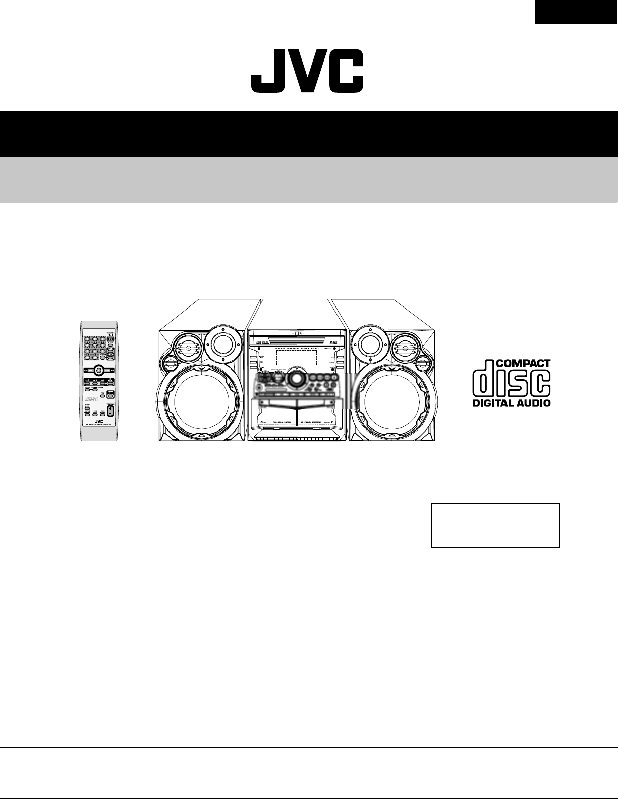
COMPACT COMPONENT SYSTEM
MX-KA7
MX-KA7
CA-MXKA7SP-MXKA7 SP-MXKA7
Contents
Safety precautions ---------------------------- 1- 2
Preventing static electricity ----------------- 1- 3
Important for laser products ---------------- 1- 4
Disassembly method ------------------------ 1- 5
Adjustment method -------------------------- 1- 18
Flow of functional
operation until TOC read -------------- 1- 20
Area Suffix
JW ........ Mexico, Panama
Maintenance of laser pickup -------------- 1- 21
Replacement of laser pickup -------------- 1- 21
Description of major ICs ------------------- 1- 22
Wiring connection ---------------------------- 1- 33
COPYRIGHT © 2003 VICTOR COMPANY OF JAPAN, LTD.
No. MB039
2003/11
Page 2
MX-KA7
1. This design of this product contains special hardware and many circuits and components specially for
2. Alterations of the design or circuitry of the product should not be made. Any design alterations of the
3. Many electrical and mechanical parts in the products have special safety-related characteristics. These
4. The leads in the products are routed and dressed with ties, clamps, tubings, barriers and the like to be
5. Leakage currnet check (Electrical shock hazard testing)
After re-assembling the product, always perform an isolation check on the exposed metal parts of the
Safety Precautions
safety purposes. For continued protection, no changes should be made to the original design unless
authorized in writing by the manufacturer. Replacement parts must be identical to those used in the
original circuits. Services should be performed by qualified personnel only.
product should not be made. Any design alterations or additions will void the manufacturer's warranty
and will further relieve the manufacture of responsibility for personal injury or property damage
resulting therefrom.
characteristics are often not evident from visual inspection nor can the protection afforded by them
necessarily be obtained by using replacement components rated for higher voltage, wattage, etc.
Replacement parts which have these special safety characteristics are identified in the Parts List of
Service Manual. Electrical components having such features are identified by shading on the
!
schematics and by (
which does not have the same safety characteristics as the recommended replacement parts shown in
the Parts List of Service Manual may create shock, fire, or other hazards.
separated from live parts, high temperature parts, moving parts and/or sharp edges for the prevention
of electric shock and fire hazard. When service is required, the original lead routing and dress should
be observed, and it should be confirmed that they have been returned to normal, after re-assembling.
product (antenna terminals, knobs, metal cabinet, screw heads, headphone jack, control shafts, etc.)
to be sure the product is safe to operate without danger of electrical shock. Do not use a line isolation
transformer during this check.
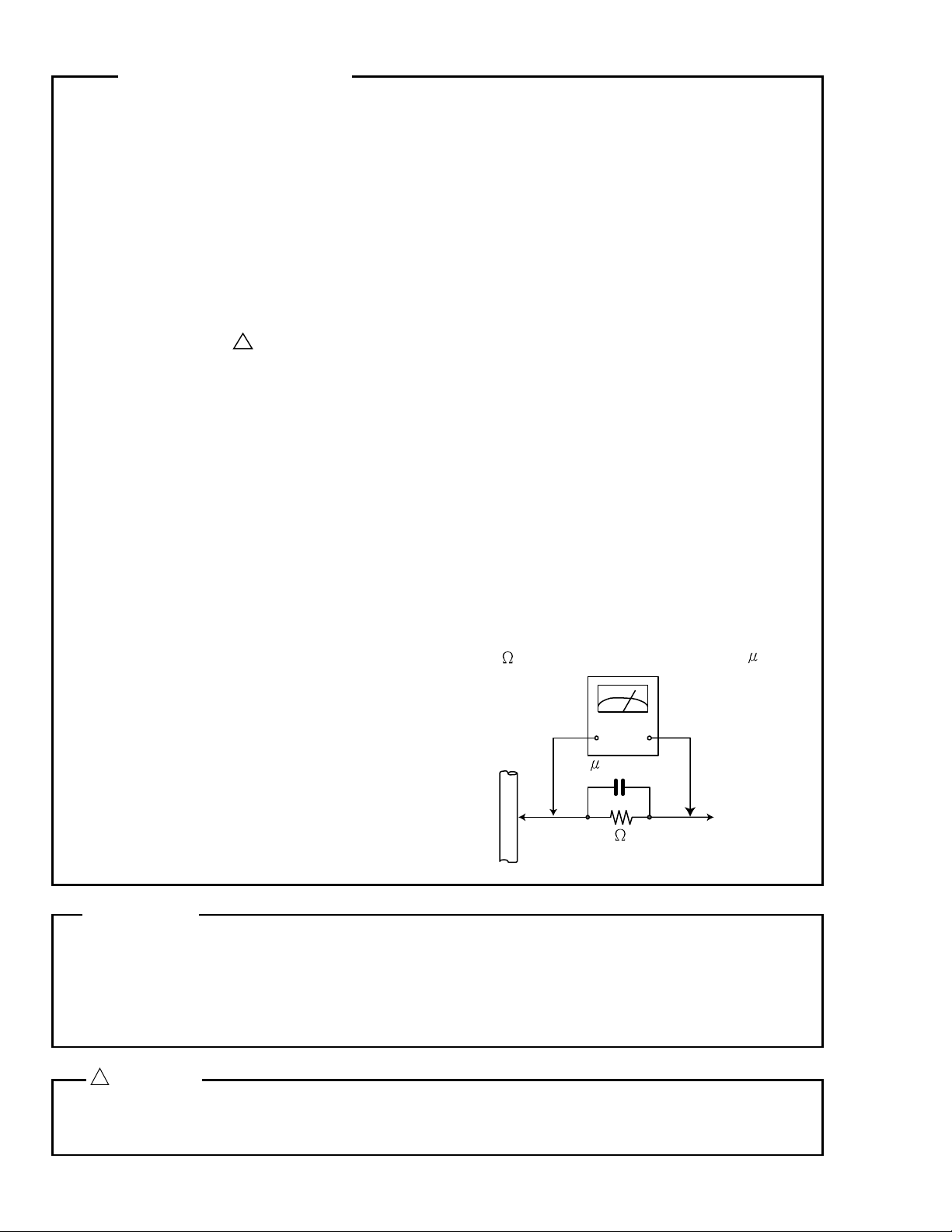
Plug the AC line cord directly into the AC outlet. Using a "Leakage Current Tester", measure the
leakage current from each exposed metal parts of the cabinet, particularly any exposed metal part
having a return path to the chassis, to a known good earth ground. Any leakage current must not
exceed 0.5mA AC (r.m.s.)
Alternate check method
Plug the AC line cord directly into the AC outlet. Use an AC voltmeter having, 1,000 ohms per volt or
more sensitivity in the following manner. Connect a 1,500 10W resistor paralleled by a 0.15 F ACtype capacitor between an exposed metal part
and a known good earth ground. Measure the AC
voltage across the resistor with the AC voltmeter.
Move the resistor connection to each exposed
metal part, particularly any exposed metal part
having a return path to the chassis, and meausre
the AC voltage across the resistor. Now, reverse
the plug in the AC outlet and repeat each
measurement. Voltage measured Any must not
exceed 0.75 V AC(r.m.s.). This corresponds to 0.5
mA AC(r.m.s.).
) on the Parts List in the Service Manual. The use of a substitute replacement
AC VOLTMETER
(Having 1000
ohms/v
olts,
or more sensitivity)
0.15 F AC TYPE
Place this
probe on
1500 10W
each exposed
metal part.
1-2
Good earth ground
Warning
1. This equipment has been designed and manufactured to meet international safety standards.
2. It is the legal responsibility of the repairer to ensure that these safety standards are maintained.
3. Repairs must be made in accordance with the relevant safety standards.
4. It is essential that safety critical components are replaced by approved parts.
5. If mains voltage selector is provided, check setting for local voltage.
!
CAUTION
Burrs formed during molding may be left over on some parts of the chassis. Therefore,
pay attention to such burrs in the case of preforming repair of this system.
Page 3
Preventing static electricity
1. Grounding to prevent damage by static electricity
Electrostatic discharge (ESD), which occurs when static electricity stored in the body, fabric, etc. is
discharged, can destroy the laser diode in the traverse unit (optical pickup). Take care to prevent this when
performing repairs.
2. About the earth processing for the destruction prevention by static electricity
In the equipment which uses optical pick-up (laser diode), optical pick-up is destroyed by the static electricity
of the work environment.
Be careful to use proper grounding in the area where repairs are being performed.
2-1 Ground the workbench
Ground the workbench by laying conductive material (such as a conductive sheet) or an iron plate over it
before placing the traverse unit (optical pickup) on it.
2-2 Ground yourself
Use an anti-static wrist strap to release any static electricity built up in your body.
(caption)
Anti-static wrist strap
MX-KA7
Conductive material
(conductive sheet) or iron plate
3. Handling the optical pickup
1. In order to maintain quality during transport and before installation, both sides of the laser diode on the
replacement optical pickup are shorted. After replacement, return the shorted parts to their original condition.
(Refer to the text.)
2. Do not use a tester to check the condition of the laser diode in the optical pickup. The testers internal power
source can easily destroy the laser diode.
4. Handling the CD changer unit (optical pickup)
1. Do not subject the CD changer unit (optical pickup) to strong shocks, as it is a sensitive, complex unit.
2. Cut off the shorted part of the flexible cable using nippers, etc. after replacing the optical pickup. For specific
details, refer to the replacement procedure in the text.
Remove the anti-static pin when replacing the CD changer
unit. Be careful not to take too long a time when attaching it
to the connector.
3. Handle the flexible cable carefully as it may break when
subjected to strong force.
4. It is not possible to adjust the semi-fixed resistor that
adjusts the laser power. Do not turn it.
CD changer
unit
Attention when traverse unit is decomposed
Please refer to “Disassembly method” in the text for
*
pick up and how to detach the CD changer mechanism.
1. Remove the CD changer unit.
2. Disconnect the harness from connector on the CD motor
board.
3. Solder is put up before the card wire is removed from connector
Cn601on the main board as shown in Fig.1 and Fig. 2.
(When the wire is removed without putting up solder, the
CD pick-up assembly might destroy.)
4. Please remove solder after connecting the card wire with
CN601 when you install picking up in the substrate.
Flexible cable
Fig.1
Soldering
Fig.2
1-3
Page 4
MX-KA7
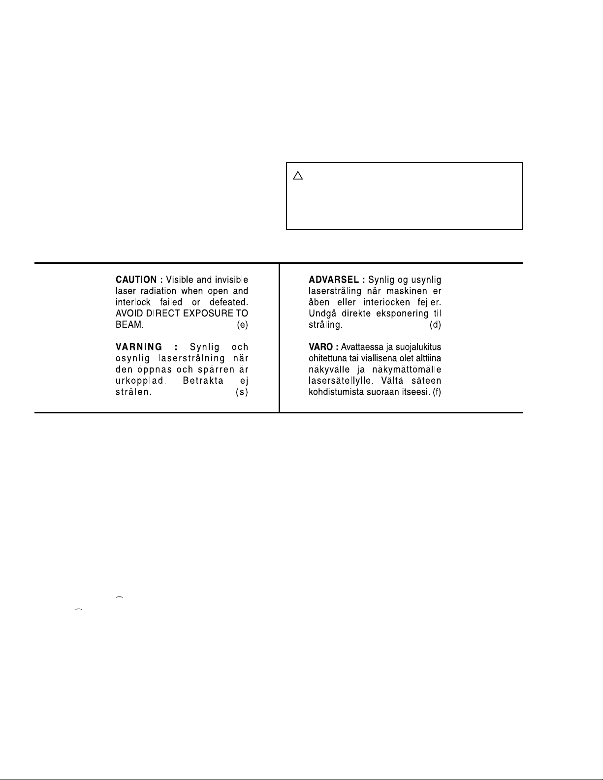
Important for laser products
1. CLASS 1 LASER PRODUCT
2. DANGER :
lock failed or defeated. Avoid direct exposure to beam.
3. CAUTION :
Laser Unit. Do not disassemble the Laser Unit. Replace
the complete Laser Unit if it malfunctions.
4. CAUTION :
laser radiation and is equipped with safety switches
which prevent emission of radiation when the drawer is
open and the safety interlocks have failed or are
defeated. It is dangerous to defeat the safety switches.
Invisible laser radiation when open and inter
There are no serviceable parts inside the
The compact disc player uses invisible
5. CAUTION :
able to function.
6. CAUTION :
of procedures other than those specified herein may
result in hazardous radiation exposure.
!
CAUTION Please use enough caution not
If safety switches malfunction, the laser is
Use of controls, adjustments or performance
to see the beam directly or touch
it in case of an adjustment or
operation check.
FUSE CAUTION
CAUTION:
REPLACE WITH SAME TYPE
AND RATING FUSE (S).
ATTENTION:
REMPLACER PAR UN(LES)
FUSIBLE(S) DE MEME TYPE
ET DE MEME VALEUR
1-4
Page 5

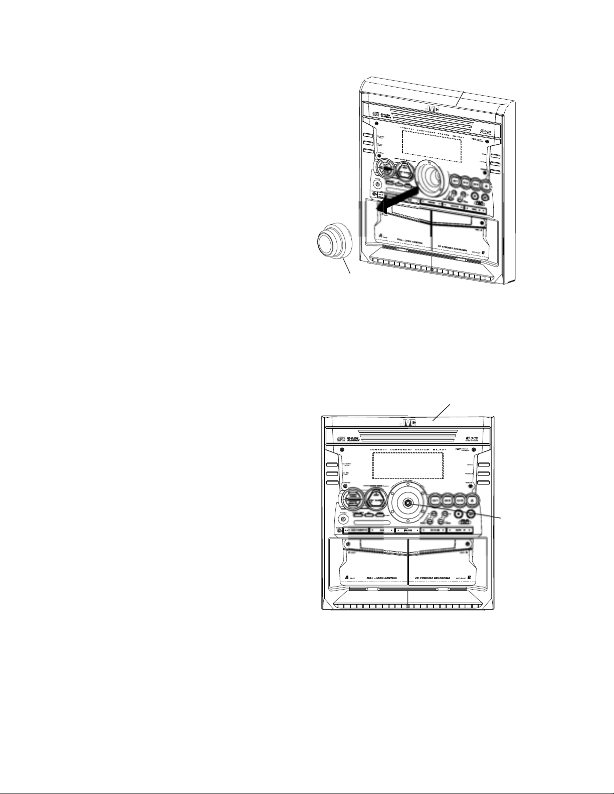
MX-KA7
Disassembly method
Commence disassembly of the set by removing the main units and then proceed to the components
and assemblies inside the units.
Replacement of the fuses and the power IC
Top cover
CD changer unit
Front panel assembly
Chassis unit
CD changer unit
Removing the main PCB
Removing the CD changer mechanism assembly
Removing the CD pickup
Replacing the loading motor and belt of the CD changer tray
Replacing the CD tray rotor belt of CD changer, and removing the motor
Front panel assembly
Removing the cassette deck mechanism
Removing the earphone jack PCB
Removing the control/FL PCB
Removing the switch PCB and ACTIVE BASS EX. switch PCB
Removing the cassette deck main motor, and replacing the main belts
Removing the leaf switches of the cassette deck mechanism
Removing the cassette deck heads
Chassis unit
Removing the 3-pin regulator
Removing the power amp and supply PCB and the Power Trans PCB
Removing the sub power PCB
1-5
Page 6
MX-KA7
<Disassembly of the main blocks of the set>
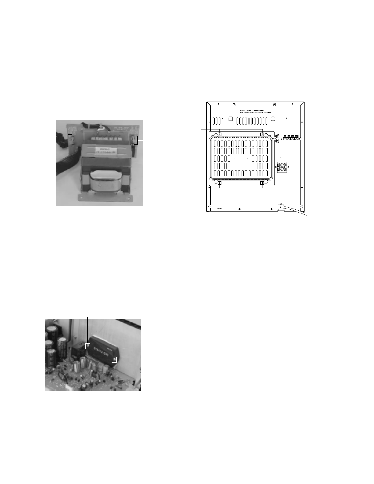
Replacement of the fuses and the power IC
Replacing the fuses (See Fig.1)
Prior to performing the following procedure, remove
the top cover.
1. Replace the fuses inside.
Replacing the heat sink cover (See Fig.3)
1. Remove four screws B from the rear panel.
2. Pull the heat sink cover outward.
[Caution]
Be sure to use fuses with the specified
ratings.
Fuse (F952)
1.6A 250V
Fig.1
Replacing the power IC (See Fig.2)
Prior to performing the following procedure, remove
the top cover.
Remove the two screws A from the heat sink between
1.
the power IC.
2. Remove the solder fixing the power IC.
B
Fuse (F951)
3.15A 250V
Fig.3
1-6
A
Fig.2
Page 7
C
Removing the top cover
(See Fig.4 and 5)
1. Remove six screws C that retain the top cover from
the panel rear of the body.
2.
Remove six screws D that retain the top cover from
the two sides of the body.
3. Remove the top cover from the body by lifting it
toward the rear.
MX-KA7
Top cover
C
Fig.4
Right Front panel assembly
Left Front panel assembly
D
D
Fig.5
D
D
1-7
Page 8
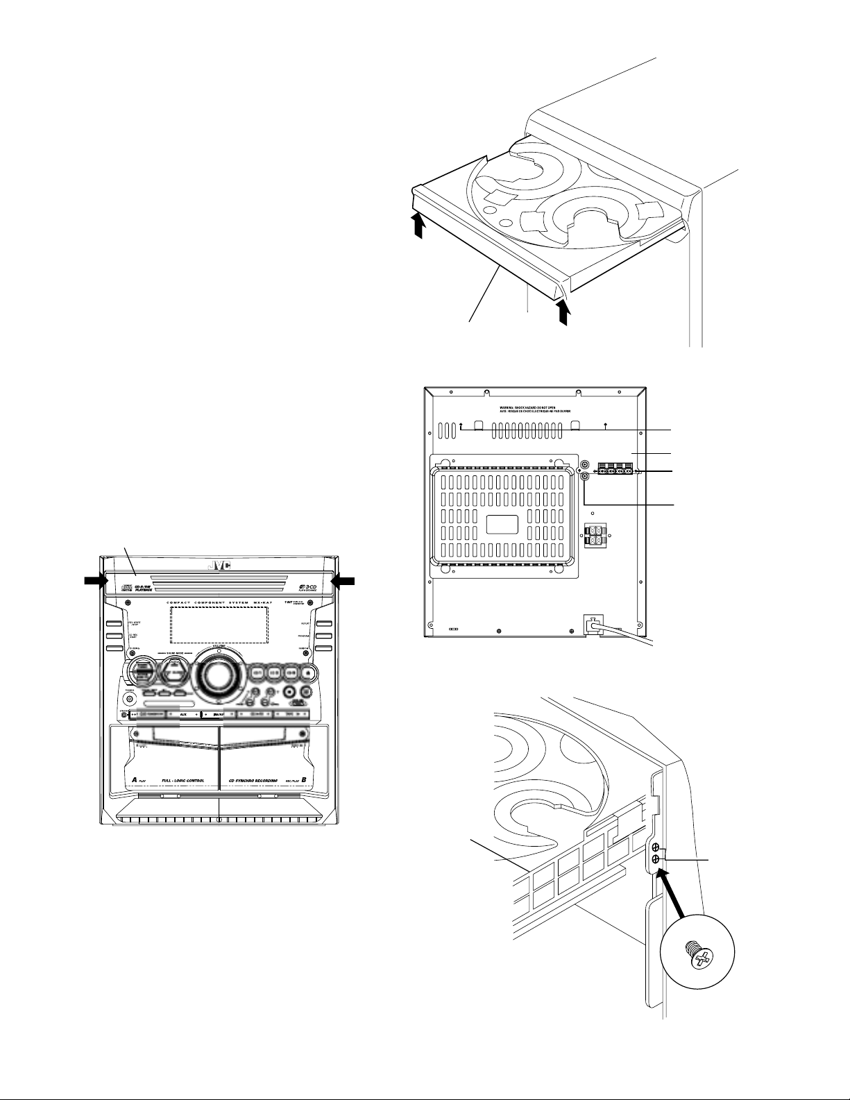
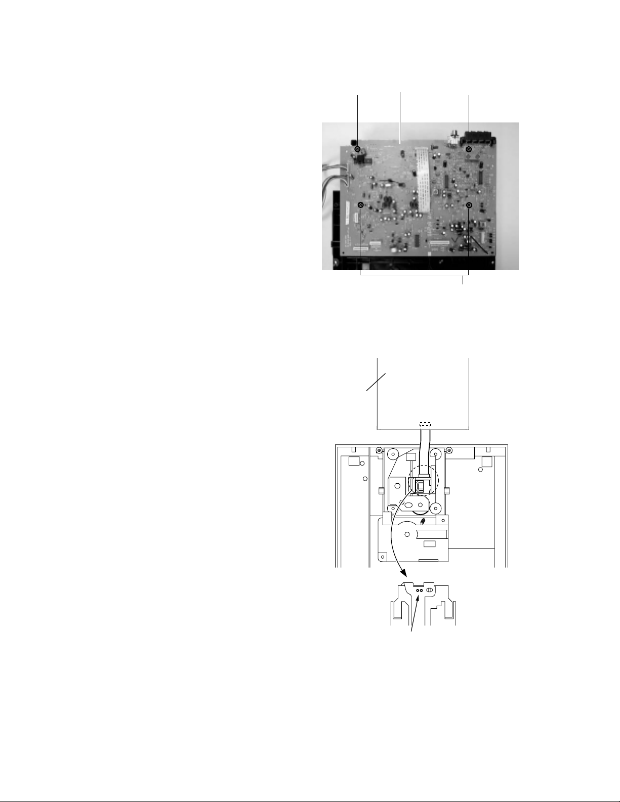
MX-KA7
Removing the CD changer unit
Prior to performing the following procedures, remove
the top cover.
(See Fig.6 to 9)
[Caution]
Although the CD mechanism unit can be
removed without removing the CD tray
panel, it is still recommended to remove it
in order to prevent damage.
a. From the front panel side of this set, push in the
sections marked with arrows and pull out the CD
tray toward the front.
b. Remove the CD tray panel by pushing both of
its extremities upward in the direction of the
arrows.
c. Push the CD tray deep into the set.
Disconnect the cord wires from the CD PCB CN703
1.
and CN203.
From the rear of the set, remove two screws E
2.
F
three screws
and four screws G on the front
panel left and right side.
3. Handle the CD changer unit rear, take out the unit.
CD tray panel
CD tray panel
Fig.7
E
Antenna
termianl
F
Aux
terminal
Fig.6
Fig.8
CD changer
unit
G
Fig.9
1-8
Page 9
Removing the front panel assembly
(See Fig.10 to 11)
Prior to performing the following procedures, remove
the top cover.
Also remove the CD changer unit.
1. Disconnect the parallel wire and the cord wire from
the connectors CN701, CN101 on the power amp.
PCB.
2. Remove one screws
assembly onto the bottom of the body.
3. Remove two screws I on the left and right side of the set
retaining the panel front from the bottom and then
remove then GND lug
amp and supply PCB.
4. Disengage the claws
panel assembly and then remove the assembly.
H
retaining the front panel
b
that comes from the power
c
on both sides of the front
MX-KA7
H
Fig.10
GND lug
Fig.11
er amp andPow
supply PCB
b
Claw
I
c
1-9
Page 10
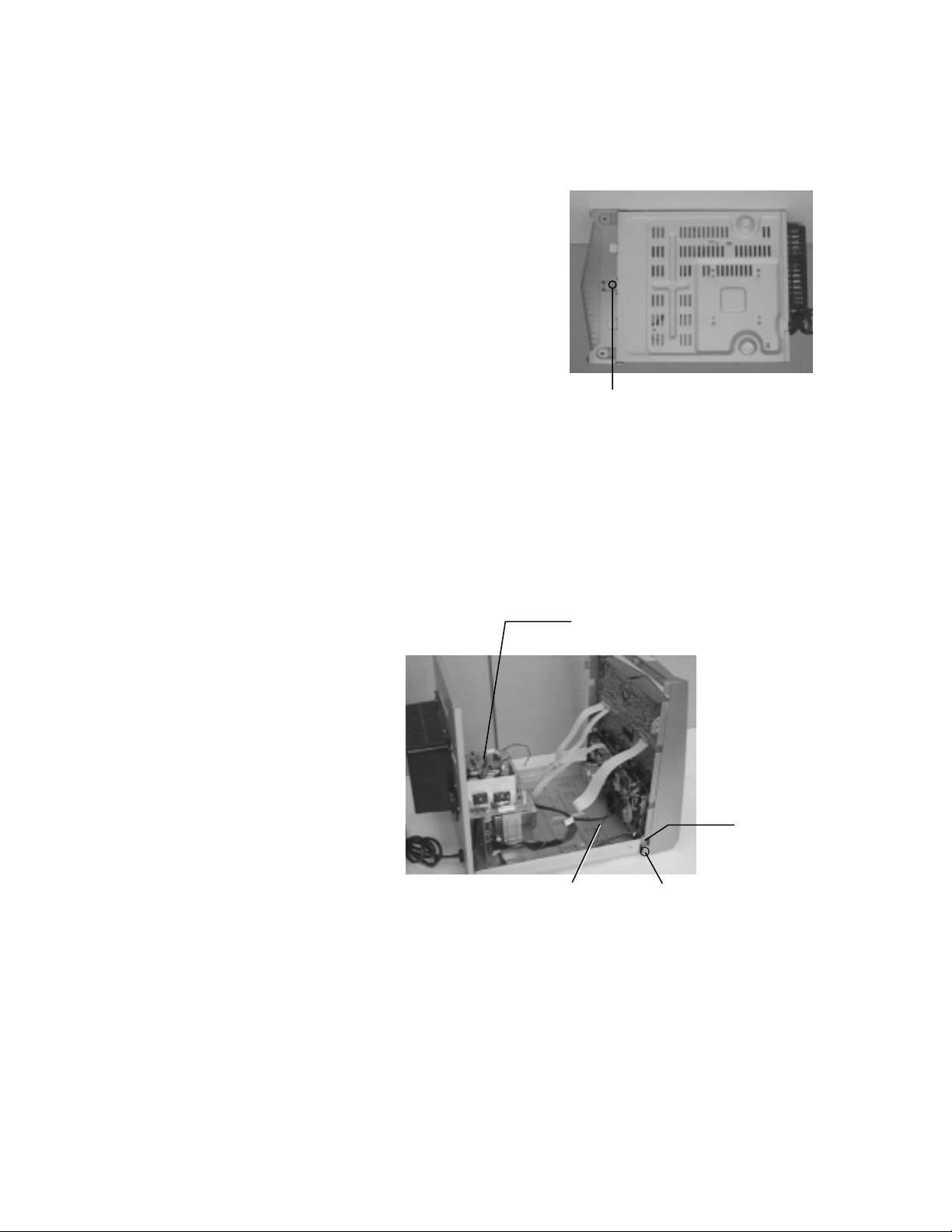
MX-KA7
<Disassembly of units and assembly
inside this set>
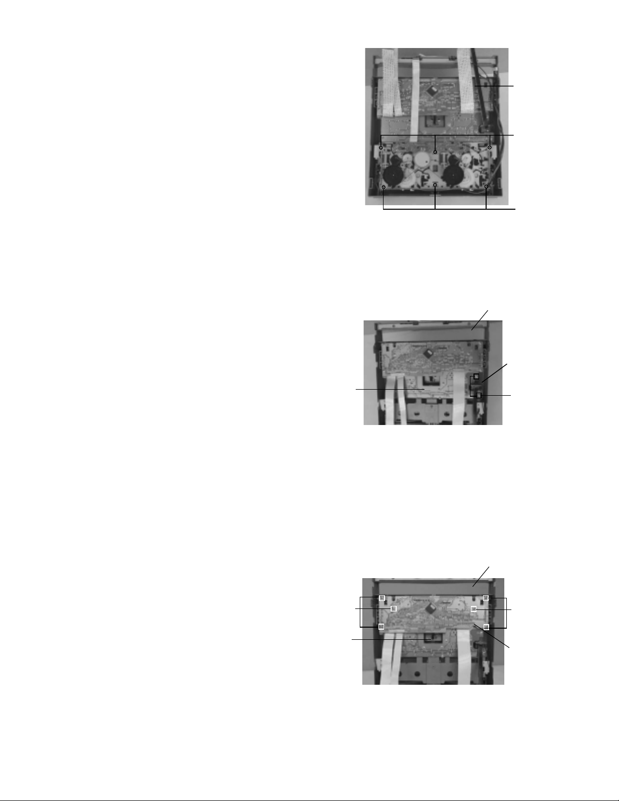
Removing the CD PCB
(See Fig.12 to 13)
Prior to performing the following procedures, remove
the top cover.
Also remove the CD changer unit.
1. Disconnect the wires from CN603A, CN603B and
CN604 on the CD PCB, which is located on the
back side of the CD changer unit.
J
2. The four screws
removed.
3. Remove the CD PCB by pulling it toward the side
where the CN601 is located.
Using solder, short the CD pickup to connect to
4.
short round.
[Caution]
After re-connecting the wires, be sure to
remove the shorting solder from the GND
connection.
5. Disconnect the card wire from the connector CN601
on the main PCB and then remove the main PCB.
that retain the CD PCB should be
J
CD PCB
CD PCB
J
J
Fig.12
CN601
Short round
Fig.13
1-10
Page 11
Removing the CD changer mechanism
assembly (See Fig.14 to 15)
Prior to performing the following procedures, remove
the top cover.
Also remove the CD changer unit.
1. Turn the CD changer mechanism cover base and
remove the screws
changer mechanism assembly.
2. Removing four screws
holder assembly.
d
connecting the unit to the CD
e
retaining the CD mechanism
MX-KA7
CD changer
unit
[Caution]
CD changer
mechanism
assemb
ly
When replacing the CD changer mechanism
assembly, be sure not to mistake the positions
of the silver color and copper color spring.
e
e
( Silver color)
( copper color)
d
Fig.14
e
( Silver color)
Fig.15
e
( copper color)
1-11
Page 12
MX-KA7
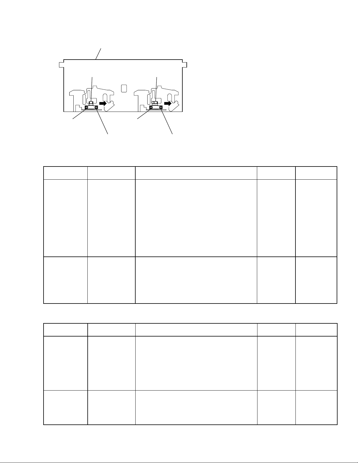
Removing the CD pickup (See Fig.16)
Prior to performing the following procedures, remove
the top cover.
Also remove the CD changer unit.
Also remove the CD changer mechanism.
CD pickup
1. Widen the section
2. While keeping the section
section
g
in the direction of the arrow to remove
f
.
f
wide open, push the
the shaft, and then remove the CD pickup.
Replacing the loading motor and rotor
belt of the CD changer (See Fig .17)
Prior to performing the following procedures, remove
the top cover.
Also open the CD changer tray.
1. Remove the two screws
L
retaining the CD
changer tray loading motor.
2. Remove the two screws
M
retaining the gear
plate and take it out, after remove the rotor belt
from the pulley.
Replacing the CD turn table and remov-
ing the motor (See Fig. 19 )
Prior to performing the following procedures, remove
the top cover.
Also remove the CD changer unit.
1. Remove the one screws
table).
2. Remove the two screws
brackets on both sides of the CD changer unit.
3. Remove the stopper brackets from both sides of
the CD changer unit.
4. Pull out the CD tray from the CD changer unit, all
the way and lift the tray (u/~ ward) to remove.
5. Remove the gear and after push out the tray motor
locker and pull out the tray motor from the CD tray.
N
retaining the CD (Turn
O
retaining the stopper
f
Shaft
Fig.16
M
L
Fig.17
g
1-12
Turn table motor
, and then remove the CD tray
Motor locker
Obligue gear
Fig.18
Page 13
Removing the cassette deck mechanism
(See Fig.19)
MX-KA7
Prior to performing the following procedures, remove
the top cover.
Also remove the CD changer unit.
Also remove the front panel assembly.
1. Remove six screws
Z
retaining the cassette deck
mechanism.
Removing the earphone jack PCB
(See Fig.20)
Prior to performing the following procedures, remove
the top cover.
Also remove the CD changer unit.
Also remove the front panel assembly.
1. Remove the screw with the washer,
retains the earphone jack PCB.
P
that
KEY 1
PCB
Front panel
assembly
Z
Z
Fig.19
Front panel
assembly
Earphone jack
PCB
P
Removing the control/FL PCB
(See Fig.21)
Prior to performing the following procedures, remove
the top cover.
Also remove the CD changer unit.
Also remove the front panel assembly.
1. Remove six screws Q that retain the control/FL PCB
from the back of the front panel unit.
Q
KEY 2
PCB
Fig.20
Front panel
assembly
Q
Control/FL
PCB
Fig.21
1-13
Page 14
MX-KA7
Removing the switch PCB and sound
mode and CD function switch PCB
(See Fig.20 to 23)
Prior to performing the following procedures, remove
the top cover.
Also remove the CD changer unit.
Also remove the front panel assembly.
1. Pull out the volume control knob from the front of
the front panel assembly.(Fig.22)
2. Remove six screws
assembly.(Fig.21)
3. Remove the control/FL PCB.
4. Remove eleven screws
PCB.(Fig.20)
5. Remove two screws
and CD function (key 2) switch PCB.(Fig.21)
Q
retaining the front panel
R
retaining the switch (key 1)
S
retaining the sound mode
Front panel assembly
Volume knob
Fig.22
Fig.23
Front panel
assembly
Volume
shaft
1-14
Page 15
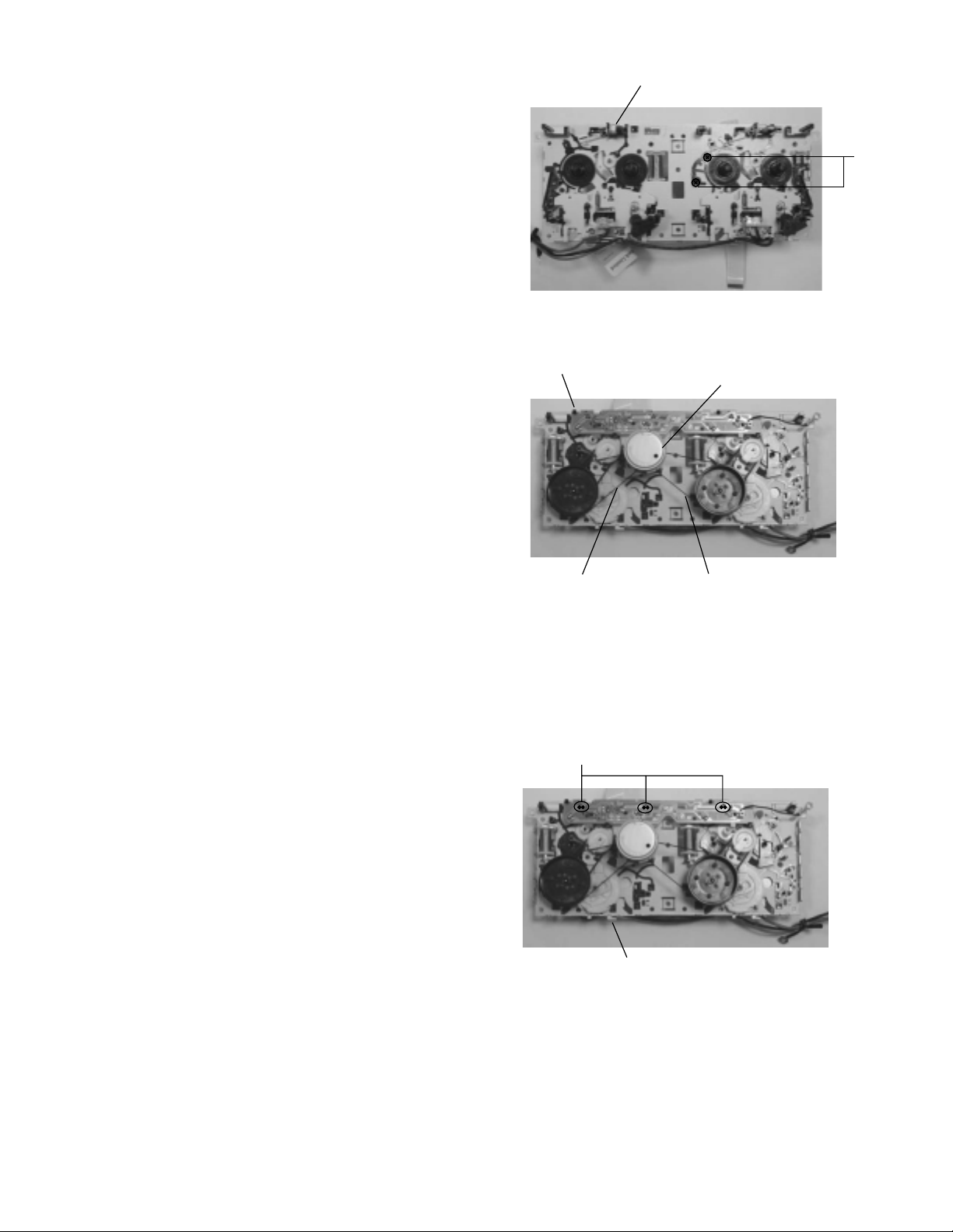
Removing the cassette deck main motor,
and replacing the main belts
(See Fig.19, 24 and 25)
Prior to performing the following procedures, remove
the top cover and both sides board.
Also remove the CD changer unit.
Also remove the front panel assembly.
Z
1. Remove six screws
mechanism. (Fig.19)
2. Remove the cassette deck mechanism.
3. Remove two screws
the front side of the cassette deck.
retaining the cassette deck
t
retaining the main motor from
MX-KA7
Cassette deck mechanism
(Front side)
t
Fig.24
[Caution]
After attaching the main motor, check the
orientation of the motor and the polarity of
the wires.
4. From the backside of the cassette deck, remove the
main motor and two main belts.
[Caution]
The lengths of the cassette A(playback
only) and cassette B(record/play) main
belts are different. When attaching the main
belts, use the longer belt for cassette
Removing the leaf switches of the cassette
A
.
deck mechanism (See Fig. 19 and 26)
Prior to performing the following procedures, remove
the top cover and both sides board.
Also remove the CD changer unit.
Also remove the front panel assembly.
Cassette deck mechanism
(Back side)
Main belt
(For B cassette)
Fig.25
Solder side of leaf switch
Cassette deck main motor
Main belt
(For
A
cassette)
1. Remove the six screws
Z
that retain the cassette
deck mechanism. (Fig.19)
2. Remove the cassette deck mechanism.
3. Turn the cassette deck mechanism upside down.
4. Remove the solder from around the leaf switches.
5. Pull out the leaf switches from the front side of the
cassette deck mechanism.
Cassette deck mechanism
(Back side)
Fig.26
1-15
Page 16
MX-KA7
Removing the cassette deck heads
Prior to performing the following procedures, remove
the top cover and both sides board.
Also remove the CD changer unit.
Also remove the front panel assembly.
(See Fig. 19 and 27)
Cassette deck mechanism
(Front side)
1. Remove six screws
Z
that retain the cassette deck
mechanism. (Fig.19)
2. Remove the cassette deck mechanism and place
it so that the front side faces up.
3. Remove the solder from the bottom side of the
head terminal and disconnect the wire.
U
4. Remove screw
5. Remove screw
that retains the head.
V
that retains the head.
6. Hold the head and slide it in the direction of the
arrow to remove it.
Removing the 3-pin regulator and bridge
diode
(See Q904, Q907, D901, D914 and Fig.28)
Prior to performing the following procedures, remove
the top cover and both sides board.
A
1. Remove two screws
2. Remove two screws
3. Remove the solder fixing the the 3-pin terminal regulator
Q904, Q907.
4. Remove the solder fixing the 4-pin bridge diode
(D901, D914).
that connect the heat sink.
W
that connect the heat sink.
PB Head REC/PB Head
V U
V U
Fig.27
AW
1-16
Fig.28
Page 17
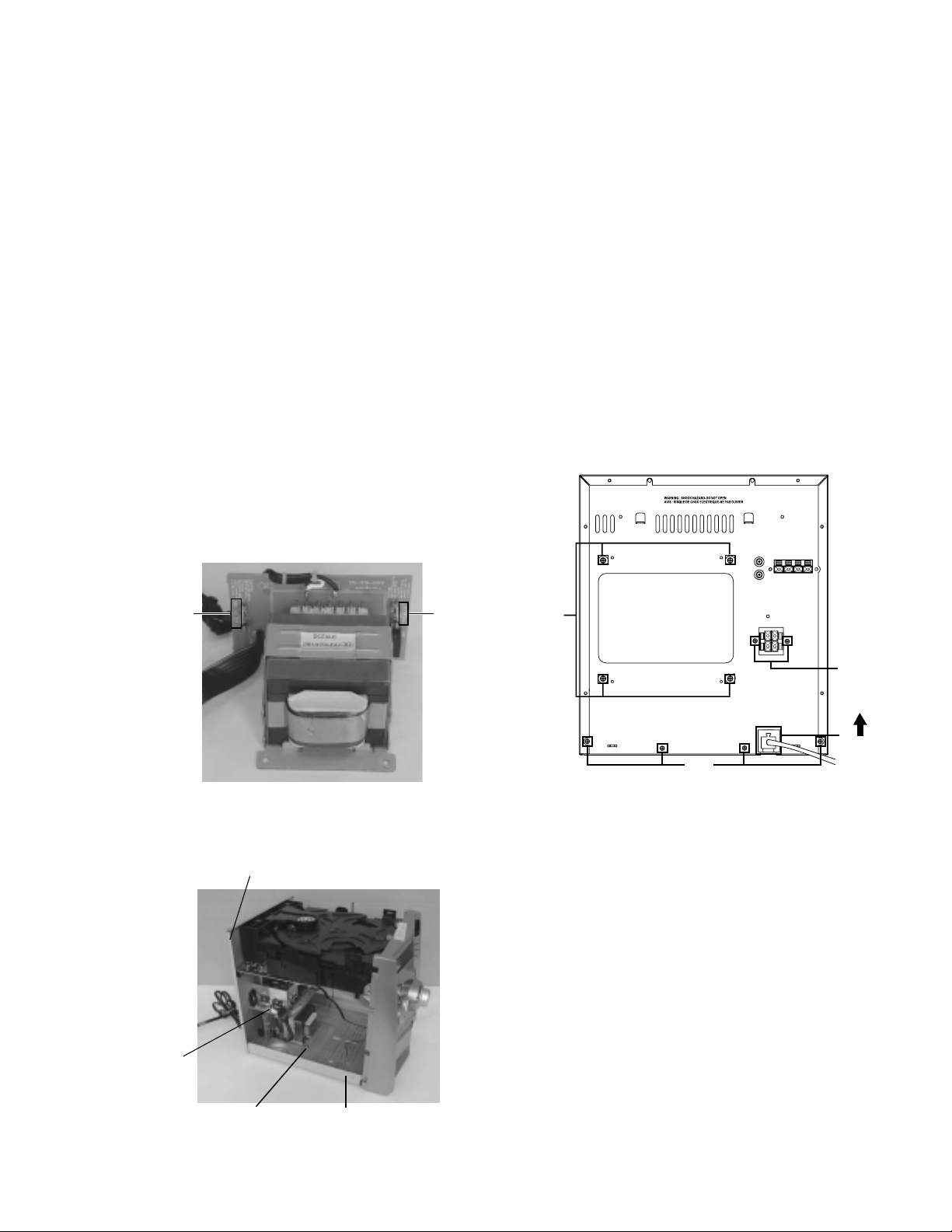
Removing the power amp and supply PCB
and the power trans PCB
(See Fig. 2, 29 to 31)
Prior to performing the following procedures, remove
the top cover and CD changer unit.
B
1. Remove four screws
2. Pull the heat sink cover outward.
3. Remove
four screws AA from the rear panel between
the heat sink holder.
4. Remove two screws X that retain the speaker terminals
and AUX terminal.
5. Remove screws
then remove the rear panel.
6. Disconnect the parallel wires from the connectors
FW951 on the power trans PCB.
7. Remove the clamp of AC power cord from the chassis.
8. Remove four screws AB that retain the power trans
PCB and then remove the assembly.
from the rear panel. (Fig.3)
YY
that retains the rear panel, and
MX-KA7
Fuse (F952)
1.6A 250V
Power amp and
supply PCB
Rear panel
Fig.29
Fuse (F951)
3.15A 250V
AA
X
Clamp
YY
Fig.30
AB
Chassis
Fig.31
1-17
Page 18

MX-KA7
Adjustment method
Measurement instruments required
for adjustment
Radio input signal
1. Low frequency oscillator.
This oscillator should have a capacity to output
0dB to 600ohm at an oscillation frequency of
50Hz-20kHz.
2. Attenuator impedance : 600ohm
3. Electronic voltmeter
4. Frequency counter
5. Wow flutter meter
6. Test tape
VT712 : For Tape speed and wow flutter ( 3kHz)
VT703 : For Head angle (10kHz)
7. Blank tape
TAPE I : AC-225 TAPE II : AC-514
8. Torque gauge : For play and back tension forward;
TW2111A, Reverse; TW2121A Fast Forward and
Rewind; TW2231A
9. Test disc: CTS-1000(12cm),GRG-1211(8cm)
10. Jitter meter
Measurement conditions
Power supply voltage
AC 120V (60Hz)
Measurement
output terminal : Speaker out
: TP101(Measuring for TUNER/
DECK/CD)
: Dummy load 6ohm
AM modulation frequency : 400Hz
Modulation factor : 30%
FM modulation frequency : 1kHz
Frequency displacement : 22.5kHz
Frequency Range
AM 530kHz~1710kHz
FM 87.5MHz~108MHz
Standard measurement positions of
volume and switch
Power : Standby (Light STANDBY Indicator)
Sound Turbo, A, BASS EX : OFF
Sound mode : OFF
Main VOL. : 0 Minimum
Travers mecha set position : Disc 1
Precautions for measurement
1. Apply 30pF and 33kohm to the IF sweeper output
side and 0.082 F and 100kohm in series to the
sweeper input side.
2. The IF sweeper output level should be made as
low as possible within the adjustable range.
3. Since the IF sweeper is a fixed device, there is no
need to adjust this sweeper.
4. Since a ceramic oscillator is used, there is no need
to perform any MPX adjustment.
5. Since a fixed coil is used, there is no need to adjust
the FM tracking.
6. The input and output earth systems are separated.
In case of simultaneously measuring the voltage in
both of the input and output systems with an
electronic voltmeter for two channels, therefore, the
earth should be connected particularly.
7. In the case of BTL connection amplifier, the minus
terminal of speaker is not for earthing. Therefore,
be sure not to connect any other earth terminal to
this terminal. This system is of an OTL system.
1-18
Page 19
Arrangement of adjusting positions
Cassette deck mechanism
(Front side)
MX-KA7
PB Head
k-A)
(Dec
Head azimuth screw
(Forward side)
Head azimuth screw
(Rev
Tape recorder section
Items
Cassette Head
Azimuth Alignments
Measurement
Test tape
: VT703 (10kHz)
Measurement output
terminal
: Left and Right
speaker output
(6-ohm loaded)
or
Headphone Output
(32-ohm loaded)
Head azimuth screw
(Forw
erse side)
conditions
REC/PB Head
(Deck-B)
ard side)
Head azimuth screw
(Reverse side)
Measurement method
1. Playback the test tape VT703 (10KHz) or equivalent.
2. Adjust the head azimuth screw to obtain maximum
output and both output of L / R is in 3dB.
3. Put on the screw lock paint after alignments.
Standard
values
Maximum output
Adjusting
positions
Adjust the
head azimuth
screw only
when the head
has been
changed.
Recording Bias
F
requency Alignment
Tuner section
Items
AM Tracking
Alignments
AM IFT Alignments
Note: The adjustment of CD section is not required.
Test tape
: TYPE I AC-514
Measurement output
terminal
: Erase head terminal
(CN308 8-Pin)
Measurement
conditions
Input signal
: 530kHz
600kHz
Adjustment point
: Antenna coil (L2)
Input signal
: 530kHz
Adjustment point
: IFT (T1)
1. Insert the recording tape in deck-B.
2. Starting the recording.
3. Adjust the oscillation frequency to 80KHz+/-3KHz by
core of Oscillation coil of L301.
1. Set the Signal Generator signal to 530KHz the feed
to Loop Antenna.
2. Receiving the signal and the adjust the OSC coil (L2)
obtain the V.T is 1.40V +/-0.05V.
3. Change the receiving frequency to 600KHz (603KHz).
4. Adjust the Antenna coil ( L2 ) obtain maximum
sensitivity. (Adjust the SSG output to out of AGC range.)
1. Set the receiving frequency to 530KHz.
2. Feed the 450KHz signal to AM antenna input.
3.Adjust the IFT Block T1 obtain to maximum output.
(Adjust the SSG output to out of AGC range.)
Measurement method
80kHz+/-3kHz
Standard
values
V. T
: 1.40V+/-0.05V
Maximum
sensitivity
Maximum output
Use the HighImpedance
Probe or
Frequency
counter input.
Adjusting
positions
Adjust the OSC
coil only when
the AM coil block
has been changed.
Adjust the IFT
only when the
IFT block has
been changed.
1-19
Page 20
MX-KA7
Flow of functional operation until TOC read
Power ON
Play Key
Slider turns REST
SW ON.
Automatic tuning
of TE offset
Check Point
Confirm that the voltage at the pin5
of CN602 is "H"\"L"\"H".
Tracking error waveform at TOC reading
Approx.3sec
Tracking
servo
off states
Automatic measurement
of TE amplitude and
automatic tuning of
TE balance
VREF
pin 20 of
IC611(TE)
Approx
0.3V
Disc states
to rotate
Tracking
servo
on states
Disc to be
braked to stop
TOC reading
finishes
500mv/div
2ms/div
Fig-1
Laser ON
Detection of disc
Automatic tuning of
Focus offset
Automatic measurement of
Focus S-curve amplitude
Disc is rotated
Focus servo ON
(Tracking servo ON)
Automatic measurement of
Tracking error amplitude
Automatic tuning of
Tracking error balance
Check that the voltage at the
pin40 of IC601 is + 5V?
Confirm that the Focus error
S-cuve signal at the pin32 of
IC601 is approx.2Vp-p
Confirm that the signal from
pin24 IC601 is 0V as a
accelerated pulse during
approx.400ms.
Confirm the waveform of
the Tracking error signal.
at the pin 20 of IC611 (R643)
(See fig-1)
1-20
Automatic tuning of
Focus error balance
Automatic tuning of
Focus error gain
Automatic tuning of
Tracking error gain
TOC reading
Play a disc
Confirm the eys-pattern
at the lead of Pin 5 of IC 611
Page 21
MX-KA7
Maintenance of laser pickup
(1) Cleaning the pick up lens
Before you replace the pick up, please try to clean
the lens with a alcohol soaked cotton swab.
(2) Life of the laser diode
When the life of the laser diode has expired, the
following symptoms will appear.
1. The level of RF output (EFM output : ampli tude of
eye pattern) will below.
Is the level of
RFOUT under
0.48V 0.1Vp-p?
NO
Replace it.
Replacement of laser pickup
Turn off the power switch and,disconnect the
power cord from the AC OUTLET.
Replace the pickup with a normal one.(Refer
to "Pickup Removal" on the previous page)
Plug the power cord in,and turn the power on.
At this time,check that the laser emits for
about 3seconds and the objective lens moves
up and down.
Note: Do not observe the laser beam directly.
Play a disc.
YES
Check the eye-pattern at
O.K
Finish.
(3) Semi-fixed resistor on the APC PC board
The semi-fixed resistor on the APC printed circuit board which is attached to the pickup is used to adjust the
laser power.Since this adjustment should be performed to match the characteristics of the whole optical
block, do not touch the semi-fixed resistor.
If the laser power is lower than the specified value, the laser diode is almost worn out, and the laser pickup
should be replaced.
If the semi-fixed resistor would be adjusted when the pickup operates normally, the laser pickup may be
damaged due to excessive current.
Pin 5 of IC 611
1-21
Page 22

MX-KA7
3
3
6
/
/
/
/
Description of major ICs STK412-030 (IC301) : Dual low noise operational
1.
Block Diagram
1
18
17
TR41
R41
1
TR1
14
TR3
15
1
TR5
R2
2.
Test Circuit
R17
TR17
R13
TR16
R16
R14
R15
C12
D12
TR11TR12
R11
TR13TR14
TR15
R12
D2
TR2
C1
R1
TR4
R3
TR6
TR7
TR8
TR9
TR10
911
812
C2 C11
R4
R5
R6
R7
D1
10
TR19
TR20
TR18
TR51
D41
D51
Comparator
Comparator
R51
SUB
D42
D4
3
2
7
D53
D52
5
4
6
+VH
+VL
GND
-VL
-VH
100uF
/50V
100uF
/50V
100uF
/100V
100uF
/100V
234567
1
GZA
15X
1.5kohm
/1W
1.5kohm
/1W
GZA
15X
SUB.GND
891011 12
*1*1*1
56kohm
3pF
100ohm/1W
100uF
/100V
100uF
/100V
100ohm/1W
*1
56kohm
3pF
13
14
560ohm
100uF
10V
16
33kohm
17
100pF100pF
560ohm
100uF
10V
3uH
4.7ohm
4.7ohm/1W
4.7ohm/1W
3uH
4.7ohm
(*1)Metal Plate Cement Resistor 0.22ohm+-10%(5W)
1815
56kohm 56kohm
2.2uF
50V
2.2uF
50V
1kohm
0.1uF
0.1uF
1kohm
Ch2 IN
GND
470pF 470pF
Ch1 IN
Ch2 OUT
GND
Ch1 OUT
1-22
Page 23

Optical disc ICs
1. Pin descriptions
MX-KA7
BA5936S. (IC621)
2. Block diagram
1-23
Page 24

MX-KA7
Optical disc ICs HA12237F (IC401)
1. Block Diagram
21222324252627282930
RECOUT(L)
NC
Test mode
(Open for normal use)
20
EQ
IREF
19
GND
18
+
V
ALC DET
17
REC MUTE OFF/ ON
CC
16
15
ALC
High/ Norm
A/
(REC Return ON/ OFF )
MUTE ON/ OFF
14
13
12
ALC ON/ OFF
11
+
1098
EQ
RECOUT(R)
NC
ALC(L)
RECIN(L)
NC
++
PBOUT(L)
38NC
BA
39
AIN(R)
MUTE
93/120
(High/Norm)
+
40
+
PB-NF1(R)
TAI(L)
EQOUT(L)
PB-EQ(L)
PB-NF2(L)
Pin Description, Equivalent Circuit (cont)
MUTE
93/120
(High/Norm)
+
31
AIN(L)
+
PB-NF1(L)
32
B
A
33
RIP
+
34
BIN(L)
Return SW
35
REC-
RETURN
GND
Return SW
36
37
BIN(R)
(VCC = 12V, Ta = 25°C, No Signal, The value in the table shows typical value.)
ALC(R)
765432
1
RECIN(R)
NC
+
TAI(R)
PBOUT(R)
EQOUT(R)
PB-EQ(R)
PB-NF2(R)
1-24
Pin No. Pin Name Note Equivalent Circuit Description
33 RIP V = VCC/2
V
CC
Ripple filter
V
GND
29
2
PB-EQ(L)
PB-EQ(R)
NAB output
Page 25

Pin Description, Equivalent Circuit
(V
CC
= 12V, Ta = 25°C, No Signal, The value in the table shows typical value.)
Pin No. Pin Name Note Equivalent Circuit Description
16 V
CC
21 RECOUT(L)
V = V
V = V
CC
/2
CC
V
CC
10 RECOUT(R)
26
PBOUT(L)
5 PBOUT(R)
28 EQOU
T(L)
V = 2.9 V
3 EQOUT(R)
GND
35 REC-RETURN REC Retu
V = 0 V
V
CC
34 BIN(L)
37 BIN(R)
PB-NF
BIN
120 k
VCC pin
output
REC
PB outpu
t
EQ output
rn
PB B deck input
MX-KA7
32 AIN(
L)
39 AIN(R)
24 RECIN(L
)
7RECIN(R)
27
TAI(L)
4TAI(R)
REC Return
V = 0 V
V
CC
PB A deck input
PB-NF
AIN
120 k
GND
V = VCC/2 REC-EQ input
V = VCC/2
V
CC
Tape input
100 k
VCC/2
1-25
Page 26

MX-KA7
Pin Description, Equivalent Circuit (cont)
(V
CC
= 12V, Ta = 25°C, No Signal, The value in the table shows typical value.)
Pin No. Pin Name Note Equivalent Circuit Description
11 ALC ON/OFF
12 High/
13 A/
14 MUTE ON/
15 REC MUTE OFF/ON
19 IREF
Norm
B
OFF
(Control
voltage = 3 V)
100 k
V = 1.2 V Equalizer refernce
I
22 k
V
GND
Mode control input
CC
current input
18, 36 GND
6, 9, 22,
25, 38
20
31 PB-NF
40 PB-NF
30 PB-NF
1 PB-NF2(R)
NC
Test mode
1(L)
1(R)
2(L)
V = 0.6 V
PBNF1
GND TEST
V
CC
330 k180
PBNF2
GND pin
NC pin
Test mode pin
PB EQ feed back
1-26
Page 27

AN22000A (IC611) : CD-DA Head Amp.
1. Terminal layout
MX-KA7
2. Pin function
1
16
3. Block diagram
RFOUT
RF_EQ
624754 8
RFIN
NRFDET
AGC
23
17
Pin
No.
Symbol
I/O
Function
1 PD I APC Amp. input terminal
2 LD O APC Amp. output terminal
3 VCC - Power supply terminal
4 RFN I RF adder Amp. inverting input
terminal
5 RFOUT O RF adder Amp. output terminal
6 RFIN I AGC input terminal
7 CAGC I Input terminal for AGC loop
filter capacitor
8 ARF O AGC output terminal
9 CBA I Capacitor connecting terminal
for HPF-Amp.
10 3TOUT O 3 TENV output terminal
11 CBOO I Capacitor connecting terminal
for envelope detection on the
darkness side
12 BDO O BDO output terminal
13 COFTR I Capacitor connecting terminal
for envelope detection on the
light side
14 OFTR O OFTR output terminal
11 12
BDO
13 14
OFTR
3TENV
9
10
Pin
No.
Symbol
I/O
Function
15 NRFDET O NRFDET output terminal
16 GND - Ground
17 VREF O VREF output terminal
18 VDET O VDET output terminal
19 TEBPF I VDET output terminal
20 TEOUT O TE Amp. output terminal
21 TEN I TE Amp. inverting input
terminal
22 FEN I FE Amp. inverting input
terminal
23 FEOUT O FE Amp. output terminal
24 GCTL O GCTL & APC terminal
25 FBAL O FBAL control terminal
26 TBAL O TBAL control terminal
27 E I Tracking signal input terminal 1
28 F I Tracking signal input terminal 2
29 D I Focus signal input terminal 4
30 B I Focus signal input terminal 3
31 C I Focus signal input terminal 2
32 A I Focus signal input terminal 1
32
31
30
29
27
28
AMP
AMP
AMP
AMP17GCA BCA
+
-
GCA BCA
GCA BCA
GCA BCA
GCTL
SUBT
SUBT
TBAL
26
FBAL
25 16 3
+
+
VDET
+
15
22
23
21
20
19
18
2
LD
PD
1
1-27
Page 28

MX-KA7
MN6627482WA (IC601) : Digital servo & digital signal processor
1. Terminal layout
80~61
1
60
20
21~40
2. Pin function
Pin
No
1 BCLK
2 LRCK
3 SRDATA
4 DVDDI
5 DVSSI
6TX
7 MCLK
8 M D ATA
9 MLD
10 SENSE
11 FLOCK
12 TLOCK
13 BLKCK
14 SQCK
15 SUBQ
16 DMUTE
17 STAT
18 RST
19 SMCK
20 PMCK
21 TRV
22 TVD
23 PC
24 ECM
25 ECS
26 KICK
27 TRD
28 FOD
29 VREF
30 FBAL
31 TBAL
32 FE
33 TE
34 RFENV
35 VDET
36 OFT
37 TRCRS
38 /RFDET
39 BDO
40 LDON
41
Symbol Function
I/O I/O
-
Not use
-
Not use
-
Not use
-
Power supply for digital circuit
-
GND for digital circuit
-
Not use
I
Micro computer command
clock signal input
I
Micro computer command
data input
I
Micro computer command
load signal input (L: Load)
-
Not use, connect to TP7
-
Not use, connect to TP6
-
Not use, connect to TP5
O
Sub code block clock
signal output
I
External clock input for sub
code Q register input
O
Sub code Q data output
I
Muting input (H: Mute)
O
Status signal input
I
Reset signal input (L: Reset)
-
Not use
-
Not use, connect to TP8
O
Traverse enforced output
O
Traverse drive output
-
Not used
O
Spindle motor drive signal
(Enforced mode output)
O
Spindle motor drive signal
(Servo error signal output)
O
Kick pulse output
O
Tracking drive output
O
Focus drive output
I
Reference voltage
for D/A output block
O
Focus balance adjust
signal output
O
Tracking balance adjust
signal output
I
Focus error signal input
(Analog input)
I
Tracking error signal input
(Analog input)
RF envelope signal input
I
(Analog input)
Vibration detect signal
I
input (H:Detect)
Off track signal input
I
(H:Off track)
Track cross signal input
I
RF detect signal input
I
(L:Detect)
Drop out signal input
I
(H:Drop out)
Laser on signal output
O
(H:ON)
Pin
Symbol Function
No
41 PLLF2
42 TOFS
43 WVEL
44 ARF
45 IREF
46 DRF
47 DSLF
48 PLLF
49 VCOF
50 AVDD2
51 AVSS2
52 EFM
53 PCK
54 VCOF2
55 SUBC
56 SBCK
57 VSS
58 X1
59 X2
60 VDD
61 BYTCK/TRVSTP
62 CLDCK
63 FCLK
64 IPFLAG
65 FLAG
66 CLVS
67 CRC
68 DEMPH
69 RESY
70 IOSEL
71 /TEST
72 AVDD1
73 OUTL
74 AVSS1
75 OUTR
76 RSEL
77 CSEL
78 PSEL
79 MSEL
80
SSEL
-
-
I
I
I
I/O
I/O
I/O
-
-
-
O
I/O
-
-
-
I
O
-
-
O
-
O
O
-
-
O
-
I
I
-
O
-
O
I
I
I
I
I
Not use
Not use
Not use
RF signal input
Reference current input
Bias pin for DSL
Loop filter pin for DSL
Loop filter pin for PLL
Loop filter pin for VCO
Power supply for analog
circuit
GND for analog circuit
Not use, connect to TP12
Clock output for PLL
Loop filter pin for Digital
servo VCO
Not use
Not use
GND for crystal oscillation
circuit
Input for crystal oscillation
circuit (f=16.9344MHz)
Output for crystal oscillation
circuit (f=16.9344MHz)
Power supply for crystal
oscillation circuit
Not use
Sub code frame clock
signal output
Not used
Interpolation flag signal
output, Connect to TP11
Flag signal output,
Connect to TP10
Not use
Not use
De-emphasis detect signal
output, Connect to TP9
Not use
Mode select pin, Connect
to DVDD1 (H fix)
Test pin, Connect to
DVDD1 (H fix)
Power supply for analog
circuit
L-channel audio output
GND for analog circuit
R-channel audio output
RF signal polarity setting pin,
Connect to DVDD1 (H fix)
Oscillation frequency setting
pin, Connect to GND (L fix)
IOSEL=H, Test pin,
Connect to GND (L fix)
IOSEL=H, SMCK output,
Frequency select pin
IOSEL=H, SMCK output,
SUBQ output mode select pin
1-28
Page 29

BA15218DIP (IC102) : Dual low noise operational amp.
1. Terminal layout
MX-KA7
OUT1
- IN1
+IN1
VEE
LA1823DIP (IC1) : 1chip AM/FM, MPX tuner system
+-
Vcc
OUT2
- IN2
-+
+IN2
1. Block diagram
24
FM
RF
AM
RF
23
GND2
REG VCC1 GND1
22
AM
MIX
AM
OSC
21
VCC2
B
UFFER
OSC
20
FM
OSC
FM
MIX
MUTE
B
UFFER
IF
ST SW
17 16
DECODER
VCO FF FF
TRIG
STSD
15
PHASE
COMP
FM
S-METERAMDET
FM
IF
14
PILOT
DET
FF
AM
IF
1319 18
FM
DET
AG
C
1 2 4 5 10 11 126 7 8 93
2. Pin function
Pin
No.
Symbol
I/O
1 AM_RFIN I AMRF signal input
2 REG. -
3 AM_OSC - AM local oscillation circuit
4 VCC_1 - Power supply terminal
FM_MIXOUT
5
O Output terminal for FM mixer
6 GND_1 - Ground
7
IF_BUFFER
O IF buffer output
8 ST_IND O Stereo indicator output
AM_MIXOUT
9
O Output terminal for AM mixer
10 FM_IF IN I Input of FMIF signal
11 AM_IF IN I Input of AMIF signal
12 AGC I AGC voltage input terminal
Function
Pin
No.
Symbol
I/O
Function
13 FM_DET O FM detection signal output
ST/MON_SW
14
AM/FM_SW
15
I Stereo/Monaural switching signal input
I AM/FM switching signal input
16 L_OUT O Output L-channel
17 R_OUT O Output R-channel
18 MPX_IN I Multiplex signal input
19 DET_OUT O AM/FM detection output
20 FM_OSC - FM local oscillation circuit
21 VCC_2 - Power supply terminal
22
FM_RFOUT
O Output of FMRF signal
23 GND_2 - Ground
24 FM_RFIN I
Input of FMRF signal
1-29
Page 30

MX-KA7
TDA7440D (IC101) : Audio processor
1. Terminal layout
2. Block diagram
4
LIN1
5
LIN2
6
LIN3
7
LIN4
3
RIN1
2
RIN2
1
RIN3
28
RIN4
RIN3
RIN2
RIN1
LIN1
LIN2 VS
LIN3
LIN4
MUXO-L
IN(L)
MUXO-R
IN(R)
BIN(R)
BOUT(R)
BIN(L)
100K
100K
100K
100K
100K
100K
100K
100K
1
2
3
4
5
6
7
8
9
10
11
12
13
14
G
0/30dB
2dB STEP
G
INPUT MULTIPLEXER
+ GAIN
MUXO-L IN(L)
MUXO-R IN(R)
RIN4
28
LOUT
27
ROUT
26
25
AGND
24
CREF23
SDA
22
SCL
21
DGND
20
TRE(R)
19
18
TRE(L)
17
N.C.
16
N.C.
15
BOUT(L)
BASS
BASS
R
R
B
B
BOUT(L)
BOUT(R)
15
SPKR ATT
SPKR ATT
RIGHT
SUPPLY
LEFT
V
REF
CREF
TRE(L)
8 9 18 14
VOLUME
VOLUME
10 11 19 12 13 23
TREBLE
2
CBUS DECODER + LATCHES
I
TREBLE
TRE(R)
BIN(L)
BIN(R)
27
LOUT
21
SCL
22
SDA
20
DGND
26
ROUT
24
VS
25
AGND
1-30
Page 31

TC74HC4094AP (IC402)
hif
MX-KA7
: 8-bit s
t and store resister
1. Terminal layout
1
ST
2
SI
3
CK
4
Q1
5
Q2
6
Q3
7
Q4
8
GND
2. Block diagram
16
V
CC
OE
15
Q5
14
Q6
13
Q7
12
Q8
11
Q'S
10
QS
9
9
QS
10
Ø
Ø
Q'S
2
SI D Q
3
CK
1
ST
15
OE
D
F/F
ØØ
Ø Ø
D
ØS
4
Q1
ØØ
Q
LATCH
ØS ØS
Q
F/F
Ø Ø
ØS
LATCH
Q
D
QØS ØS
5
Q2
DQ
F/F
Q
Ø Ø
D
TCH
LA
Q
ØS ØS
6
Q3
DQ
F/F
Q
Ø Ø
D
TCH
LA
Q
ØS ØS
7
Q4
DQ
F/F
Q
Ø Ø
D
TCH
LA
Q
ØS ØS
14
Q5
DQ
F/F
Q
Ø Ø
D
TCH
LA
Q
ØS ØS
13
Q6
DQ
F/F
Q
Ø Ø
D
TCH
LA
Q
ØS ØS
12
Q7
DQ
F/F
Q
Ø
Ø
D
TCH
LA
Q
ØS ØS
11
Q8
Ø
Ø
1-31
Page 32

MX-KA7
LC72136N (IC2) : PLL Frequency synthesizer
1.Terminal layout
1
CLOCK
VCOSTOP
AM/FM
MW
SDIN
2. Block diagram
XTI
FM
CE
DI
DO
LW
2
3
4
5
6
7
8
9
10
11
22
21
20
19
18
17
16
15
14
13
12
XT
GND
LPFI
LPFO
PD
VCC
FMIN
AMIN
NC
IFCNT
IFIN
1
22
16
15
3
4
5
6
17
21
3. Pin function
Pin
Symbol
No.
XTI
1
FM
2
CE
3
4
5
6
7
8
9
10
11
DI
CLOCK
DO
VCOSTOP
AM/FM
NC
NC
SDIN
Reference
Driver
Swallow Counter
1/2
2
B
C
I/F
Power
on
Reset
Function
I/O
X'tal oscillator connect (75KHz)
I
LOW:FM mode
O
When data output/input for 4pin(input) and
I
Swallow Counter
1/16,1/17 4bit
1/16,1/17 4bit
12bit
Programmable
DriverS
Data Shift Register & Latch
7821113
6pin(output): H
Input for receive the serial data from
I
controller
Sync signal input use
I
Data output for Controller
O
Output port
"Low": MW mode
O
Open state after the power on reset
O
Input/output port
-
Input/output port
-
Data input/output
I/O
Phase
Detector
Charge Pump
Unlock
Detector
Universal
Counter
Pin
No.
12
13
14
15
16
17
18
19
20
21
22
Symbol
IFIN
IFCNT
NC
AMIN
FMIN
VCC
PD
LPFO
LPFI
GND
XT
18
19
20
12
I/O
Function
IF counter signal input
I
IF signal output
O
Not use
-
AM Local OSC signal output
I
FM Local OSC signal input
I
Power supply(VDD=4.5 5.5V)
-
When power ON:Reset circuit move
PLL charge pump output(H: Local OSC
O
frequency Height than Reference frequency.
L: Low Agreement: Height impedance)
Output for active lowpassfilter of PLL
O
Input for active lowpassfilter of PLL
I
Connected to GND
-
X'tal oscillator(75KHz)
I
1-32
Page 33

MX-KA7
Wiring
5
4
connection
P/N : BI12P60143U
P/N : BI1203941
P/N : BI12P80102U
P/N : BI1205281U
3
P/N : BI1205251U
P/N : BI1205441U
P/N : BI12P30215U
P/N : BI1205241U
P/N : BI12P40251U
P/N : BI12P90055U
2
1
AB C
P/N : BI1205291U
P/N : BI1205261U
P/N : BI12P100035U
P/N : BI12P60142U
1-33
Page 34

MX-KA7
VICTOR COMPANY OF JAPAN, LIMITED
AV & MULTIMEDIA COMPANY AUDIO/VIDEO SYSTEMS CATEGORY 10-1,1Chome,Ohwatari-machi,Maebashi-city,371-8543,Japan
No.MB039
Printed in Japan
WPC
Page 35

n Tuner section
MX-KA7
2-1
Page 36

n Main section
MX-KA7
2-2
Page 37

n CD section
MX-KA7
2-3
Page 38

n Amplifier
MX-KA7
2-4
Page 39

n FL Display and CPU Control
MX-KA7
2-5
Page 40

n
Power transformer section
MX-KA7
2-6
Page 41

n Block diagram
MX-KA7
2-7
Page 42

n Wiring diagram
MX-KA7
2-8
Page 43

n Main top PWB
MX-KA7
2-9
Page 44

n Main bottom PWB
MX-KA7
2-10
Page 45

n FL Display and CPU (TOP)
MX-KA7
2-11
Page 46

n FL Display and CPU (BOTTOM)
MX-KA7
2-12
Page 47

n Power Amp. PWB
MX-KA7
2-13
Page 48

n Power trans PWB
MX-KA7
2-14
Page 49

PARTS LIST
t
[ MX-KA7]
* All printed circuit boards and its assemblies are not available as service parts.
Area suffix
JW -------------- Mexico,Panama
MB039
- Contents -
Exploded view of general assembly and parts list (Block No.M1)
CD changer mechanism
Cassette mechanism assembly
Electrical parts list (Block No.01~05)
Packing materials and accessories parts list (Block No.M3)
assembly and parts list (Block No.MA)
and parts list (Block No.MP)
3- 2
3- 5
3- 7
3- 8
3-12
- Note-
Parts number of normal capacitors and normal resistors doesn't listed on the parts lis
3-1
Page 50

Exploded view of general assmbly and parts list
e
1
Block No.
64
M
M
1
M
38
34
22
Main board
Vol board
61
54
52
VFD board
56
Headphone
board
54
22
51
36
17
20
51
Front
33
55
58
7
6
62
59
29
18
54
board
41
57
3
51
24
8
5
15
50
30
9
20
4
65
51
35
64
64
AMP
board
26
54
32
31
64
53
64
54
5
27
14
Pow
boa
66
23
16
2
39
21
49
60
37
10
11
12
25
55
54
13
3-2
Page 51

Block No.
M
M
1
M
38
oard
rd
64
1
54
52
VFD board
56
Headphone
board
51
Front
33
51
36
55
58
17
7
6
62
board
57
3
51
24
8
5
15
50
51
35
64
64
AMP
board
54
32
64
53
64
54
64
54
28
31
64
52
54
63
19
52
59
29
20
18
54
54
22
30
41
9
20
4
65
26
27
14
40
63
Power
board
66
23
3-3
Page 52

General assembly
Block No. [M][1][M][M]
Symbol No.
1 ------------ CD CHANGER MACH
2 BI109835010201 BADGE JVC
3 BI300856010101 BELT CLIP WASHE
4 BI301789010101 BUSHING 5RF-5B
5 BI107475030101 CAP CD3
6 BI107475020101 CAP CD2
7 BI107475010101 CAP CD1
8 BI107475040101 CAP OPEN CLOSE
9 BI201789010102 CASS LOCK SPRIN (x2)
10 BI107468010101 CASS DOOR WIN L
11 BI107467010101 CASS DOOR WIN R
12 BI107466010101 CASSETTE HLDE L
13 BI107465010101 CASSETTE HLDR R
14 ------------ CASSETTE MECHA CMAT6Z219A
15 BI107477010101 CD EJECT BUTTON
16 BI107463010101 CD FITTING
17 BI107471010101 CD SE BUTTON A
18 BI202547010101 CHAS MAIN
19 BI107483010101 COVER HTSINK
20 BI301388010101 DAMPING GEAR (x2)
21 BI1074640801U1 DISPLAY WINDOW
22 BI103362020102 EVA FOOT (x2)
23 BI301779010101 EVA FOOT C (x2)
24 BI107473010101 FRAME CD SELECT
25 BI107462010201 FRONT PANEL
26 BI402991 FUSE 1.6A 250V F952
27 BI403011 FUSE 3.15A 250V F951
28 BI202556010101 HEAT SINK 2
29 BI104143010102 HLDR LOCK L
30 BI104143010202 HLDR LOCK R
31 BI202560010101 HLDR R
32 BI202553010101 HLDR L
33 BI107480010101 HLDR SOUND MODE
34 BI202592010101 HOLDER BRACKET
35 BI202555010101 HEAT SINK AMP
36 BI107485010101 INDICATOR STAND
37 BI109819030201 KNOB VOLUME TAB
38 BI202548010101/S/ METAL COVER
39 BI301922010101 MIRROR SHEET
40 BI2025500301U1 REAR PANEL
41 BI104142010102 PLATE LOCK 1
49 BI107482010101 RING VOLUME
50 BIPMW001101S3 SCREW 4.0XL6 METAL(x4)
51 BIBT000418 SCREW
52 BIRT000617B3 SCREW
53 BIBT0006091 SCREW
54 BIRM000603S3 SCREW
55 BIKT000627 SCREW (x4)
56 BI107470010101 SELECT BUTTON
57 BI107469010101 SELECT BUTTON
58 BI107472010101 SOUND MODE BUTT
59 BI107478010101 SOURCE BUTTON
60 BI202566010101 SPRING L
61 BI202565010101 SPRING R
62 BI107476010101 SUB BUTTON SET
63 BIRM000604S3 SCREW RH/TS 3XL8(x8)
64 BIRT000611B3 SCREW RH/TS 3XL8(x17)
65 BI1400864 POWER CORD
66 BI211041004001W POWER TRANS T951
Part No. Part Name Description Local
2.6XL8
PLASTIC(x23)
3.0XL10
PLASTIC(x14)
3.0XL14
PLASTIC(x2)
3.0XL6
METAL(x19)
3-4
Page 53

CD changer mechanism assembly and parts list
BI3400931
7
8
Block No.
6
M
M
M
A
23
24
25
28
26
9
10
2
12
13
11
1
3
15
17
14
19
27
29
16
21
37
38B
18
20
38A
36
22
4
5
37
37
38A
37
35
33
34
32
38B
39
3-5
Page 54

CD changer mechanism
Block No. [M][A][M][M]
Symbol No.
1 BIAJ7200601J BASE-MAIN 1X1
2 BIAJ6100601P BRKT-CHUCK
3 BI3302000158 MAGNET-FERRITE
4 BIAJ7200601L TABLE-CHUCK 1X4
5 BIAJ6300601A SHEET-CHUCK (x3)
6 BIAJ7300601B BELT-LOAD
7 BIAJ6600601N GEAR-SYNCRO 1X2
8 BIAJ6600601L GEAR-CONVERT 1X4
9 BIAJ6600601M GEAR-TRAY 1X4
10 BIAJ6600601R GEAR-CAM 1X2
11 BIAJ6600601K GEAR-LOAD 1X4
12 BIAJ6600601J GEAR-PULLEY 1X4
13 BIAJ7200601N SLIDER-CAM 1X4
14 BI3405000101 SWITCH-MICRO (x2)
15 BI3711003379
16 BIAJ4100601K PCB-SW
17 BIAJ6100601K PULLEY-MOTOR 1X4
18 BIAJ3100601F MOTOR-DC
19 BI3710001248 CONNECTOR-SOCE
20 BI3711003692
21 BI3708001163 CONNECTOR-FPC
22 BIAJ4100601L PCB-MECHA
23 BIAJ7200601P TRAY- ROULETTE 1X2
24 BIAJ7200601Q TRAY-DISC 1X2
25 BIAJ6600601Q GEAR-ROULETTE 1X4
26 BIAJ6600601P GEAR-WORM 1X2
27 BIAJ3100601K MOTOR-LOADING
28 BIAJ6300601B SHEET-MOTOR
29 BIAJ3900601A WIRE-ROULETTE
32 BIAJ3900601B WIRE-TRAY
33 BI3711000003
34 BIAJ4100601J PCB-SENSOR
35 BIAJ3200601A SENSOR-ROULETTE
36 BIAJ9050605F CMS-B31NG6U
37 BIAJ6000601F SCREW (x4)
38A BIAJ7300601F RUBBER-B31Y (x2)
38B BIAJ7300601D RUBBER-B31 (x2)
39 BIAJ7200602F LEVER-LIFTER 1X2
Part No. Part Name Description Local
CONNECTORHEADE
CONNECTORHEADE
CONNECTORHEADE
3-6
Page 55

Cassette mechanism assembly and parts list
y
)
CMAT6Z219A
L SIDE
TYPE
10
L SIDE
Block No.
M
M
M
P
3
9
4
2
5
4
8
6
8
5
7
1
R SIDE
Casette mechanism
Block No. [M][P][M][M]
Symbol No.
1 BIF513858 PLATE HD BLK
2 BIF525346 MTR MAIN BLK
3 BIF567843 PCB CONTROL BLK
4 BIUE20P12 LEAF SWITCH (x3)
5 BIF522063 CLUTCH ASY BLK (x2)
6 BIFF19N31 MAIN BELT
7 BIF51435 ROLLIER PINCH B (x2)
8 BIFF19S31 F/R BELT MO (x2)
9 BIFF19N22 MAIN BELT
10 BIF513855 PLATE HD BLK
Part No. Part Name Description Local
7
R SIDE
TYPE
Note: Parts listed on the Parts List below can be supplied.
However, parts that are not listed below cannot be supplied
individually but only by purchasing the whole Cassette
Mechanism Assembly Unit. (When ordering, use the Parts No.
CMAT6Z219A for Cassette Mechanism Assembl
Unit.
3-7
Page 56

Electrical parts list
AMP. board
Symbol No.
C901 BICM682101KP015 M CAPACITOR
C902 BICM682101KP015 M CAPACITOR
C903 BICM682101KP015 M CAPACITOR
C904 BICM682101KP015 M CAPACITOR
C905 BICE33865M2 E CAPCITOR
C906 BICE33865M2 E CAPCITOR
C923 BICM682101KP015 M CAPACITOR
C924 BICM682101KP015 M CAPACITOR
C925 BICM682101KP015 M CAPACITOR
C926 BICM682101KP015 M CAPACITOR
C927 BICE47835M61 E CAPCITOR
C928 BICE47835M61 E CAPCITOR
CN307 BI12S90024U FFC CONNECTOR
CN701 BI12S110020 CONNECTOR
CN951 BI12S90025U CONNECTOR
D304 1SS133 DIODE
D305 1SS133 DIODE
D325 1SS133 DIODE
D326 1SS133 DIODE
D327 1SS133 DIODE
D331 1SS133 DIODE
D333 1SS133 DIODE
D334 MTZJ15C ZENER DIODE
D335 MTZJ15C ZENER DIODE
D336 1SS133 DIODE
D901 G5SBA60L DIODE
D902 FR202 RECTIFIER DIODE
D903 FR202 RECTIFIER DIODE
D904 FR202 RECTIFIER DIODE
D905 FR202 RECTIFIER DIODE
D906 1N4001 DIODE
D907 UZ36BSA DIODE ZENER
D908 MTZJ6.2B DIODE ZENER
D909 1SS133 DIODE
D910 MTZJ6.2B DIODE ZENER
D911 MTZJ5.6B DIODE ZENER
D912 MTZJ13B ZENER DIODE
D913 MTZJ12C DIODE ZENER
D914 RS402M RECTIFIER
D916 1SS133 DIODE
IC304 STK412-030 IC
L101 BI2601141 COIL
L201 BI2601141 COIL
PWB BI251227G01V AMP PWB
Q103 KTC3199GR TRANSISTOR
Q104 KTA1267GR TRANSISTOR
Q105 KTC3199GR TRANSISTOR
Q203 KTC3199GR TRANSISTOR
Q204 KTA1267GR TRANSISTOR
Q205 KTC3199GR TRANSISTOR
Q307 KTC3199GR TRANSISTOR
Q334 KRA107M TRANSISTOR
Q335 KRA107M TRANSISTOR
Q336 KTC3199GR TRANSISTOR
Q337 KTC3199GR TRANSISTOR
Q338 KTC3199GR TRANSISTOR
Q339 DTC114YS TRANSISTOR
Q901 8550C SI.TRANSISTOR
Q902 DTC114YS TRANSISTOR
Q903 DTC114YS TRANSISTOR
Q904 KTB1366 TRANSISTOR
Q905 KTC3199GR TRANSISTOR
Q906 KTC3199GR TRANSISTOR
Q907 KTB1366 TRANSISTOR
Q909 KRA107M TRANSISTOR
Q911 KTC3199GR TRANSISTOR
Q912 DTC114ES TRANSISTOR
R390 1SS133 DIODE
RY301 BI8RL00071 RELAY
Part No. Part Name Description Local
Block No. [0][1][0][0]
Wiring diagram
Symbol No.
CN305 BI1205441U FF-CABLE
CN306 BI1205261U FF-CABLE
CN309 BI1205241U FF-CABLE
CN601 BI1205291U FF-CABLE
CN604 BI1205251U FF-CABLE
CN701 BI1205281U FF-CABLE
DECK BI11AT065B0U WIRE
DECKA BI12P30215U WIRE
DECKB BI12P80102U WIRE
Part No. Part Name Description Local
Front board
Symbol No.
CN701 BI12S110021 FFC CONNECTOR
CN702 BI12P60143U CONNECTOR. WIRE
CN703 BI12P60143U CONNECTOR. WIRE
CN704 BI1203941 CABLE
CN705 BI1203941 CABLE
CN706 BI12S160034U FFC CONNECTOR
CN707 BI12S210005 FFC CONNECTOR
D1051 1SS133 DIODE
D1052 1SS133 DIODE
D701 1SS133 DIODE
D702 1SS133 DIODE
D703 1SS133 DIODE
D705 1SS133 DIODE
D706 1SS133 DIODE
FL701 BI2701941 FL DISPLAY
HJ105 BI2301211 MINI JACK
IC701 MN101C35D IC
IC702 RPM7140 IC
L1051 BI26047000KM002 FIXED INDUCTOR
L1052 BI26047000KM002 FIXED INDUCTOR
L1053 BI18A843556N000 F-BEAD
L702 BI26100000KM002 FIXED.INDUCTOR
L703 BI18A843556N000 F-BEAD
L707 BI26100000KM002 FIXED.INDUCTOR
LE701 BI28B4531EP0110 RED LED
P1 BI11AT160B0U BLACK WIRE
PWB BI251205G02V FRONT PCB
Q704 KTC3195Y TRANSISTOR
Q705 KTC3195Y TRANSISTOR
Q711 KRA102M TRANSISTOR
Q713 DTC114YS TRANSISTOR
Q716 DTC114TK TRANSISTOR
Q717 DTC114TK TRANSISTOR
Q718 DTC114TK TRANSISTOR
Q719 DTC114TK TRANSISTOR
Q720 DTC114TK TRANSISTOR
Q721 DTC114TK TRANSISTOR
Q722 DTC114TK TRANSISTOR
Q723 DTC114TK TRANSISTOR
Q724 DTC114TK TRANSISTOR
Q725 DTC114TK TRANSISTOR
Q726 DTC114TK TRANSISTOR
Q727 DTC114TK TRANSISTOR
Q728 DTC114TK TRANSISTOR
S1 BI8EVQ21405P015 TACT SWITCH
S1002 BI8EVQ21405P015 TACT SWITCH
S1003 BI8EVQ21405P015 TACT SWITCH
S1004 BI8EVQ21405P015 TACT SWITCH
S1005 BI8EVQ21405P015 TACT SWITCH
S1006 BI8EVQ21405P015 TACT SWITCH
S1007 BI8EVQ21405P015 TACT SWITCH
S1008 BI8EVQ21405P015 TACT SWITCH
S1009 BI8EVQ21405P015 TACT SWITCH
Part No. Part Name Description Local
Block No. [0][2][0][0]
Block No. [0][3][0][0]
3-8
Page 57

Symbol No.
Part No. Part Name Description Local
Symbol No.
Part No. Part Name Description Local
S1010 BI8EVQ21405P015 TACT SWITCH
S1011 BI8EVQ21405P015 TACT SWITCH
S1012 BI8EVQ21405P015 TACT SWITCH
S1013 BI8EVQ21405P015 TACT SWITCH
S1014 BI8EVQ21405P015 TACT SWITCH
S1015 BI8EVQ21405P015 TACT SWITCH
S1016 BI8EVQ21405P015 TACT SWITCH
S1017 BI8EVQ21405P015 TACT SWITCH
S1018 BI8EVQ21405P015 TACT SWITCH
S1019 BI8EVQ21405P015 TACT SWITCH
S1020 BI8EVQ21405P015 TACT SWITCH
S1021 BI8EVQ21405P015 TACT SWITCH
S1022 BI8EVQ21405P015 TACT SWITCH
S1023 BI8EVQ21405P015 TACT SWITCH
S2 BI8EVQ21405P015 TACT SWITCH
S701 BI8EVQ21405P015 TACT SWITCH
S702 BI8EVQ21405P015 TACT SWITCH
S703 BI8EVQ21405P015 TACT SWITCH
S704 BI8EVQ21405P015 TACT SWITCH
S705 BI8EVQ21405P015 TACT SWITCH
S706 BI8EVQ21405P015 TACT SWITCH
SW701 BI804221 JOG SWITCH
V1051 BI12P40251U CONNECTOR. WIRE
X701 BI29ZTA 8.00P 015 CERAMIC RESONTO
X702 BI2102471 CRYSTAL
Main board
Symbol No.
BF601 BI18A843556N000 F-BEAD
CF1 BI29LT10.7MP015 C.FILTER
CF2 BI29LT10.7MP015 C.FILTER
CF3 BI29JT10.7MP015 C.FILTER
CN305 BI12S110023U FFC CONNECTOR
CN306 BI12S90024U FFC CONNECTOR
CN307 BI12S30039 CONNECTOR
CN308 BI12S80024 CONNECTOR
CN309 BI12S210004 FFC CONNECTOR
CN601 BI12S160031 FFC CONNECTOR
CN602 BI12P60142U CONNECTOR.WIRE
CN603 BI12P100035U CONNECTOR.WIRE
CN604 BI12S160033U FFC CONNECTOR
D1 1SS133 DIODE
D10 1SS133 DIODE
D2 1SS133 DIODE
D3 1SS133 DIODE
D306 MTZJ9.1B ZENER DIODE
D307 MTZJ5.1B ZENER DIODE
D308 1SS133 DIODE
D309 1SS133 DIODE
D310 1SS133 DIODE
D311 1SS133 DIODE
D312 1SS133 DIODE
D313 1SS133 DIODE
D314 1SS133 DIODE
D321 1SS133 DIODE
D322 1SS133 DIODE
D323 1N4001 DIODE
D324 1SS133 DIODE
D328 1SS133 DIODE
D329 1SS133 DIODE
D330 1SS133 DIODE
D4 1SS133 DIODE
D401 1SS133 DIODE
D402 1SS133 DIODE
D5 1SS133 DIODE
D50 1SS133 DIODE
D51 1SS133 DIODE
D6 1SS133 DIODE
D605 1N4001 DIODE
D7 SVC203 VARASTOR.DIODE
D8 SVC203 VARASTOR.DIODE
Part No. Part Name Description Local
Block No. [0][4][0][0]
D9 1SS133 DIODE
IC1 LA1823 IC
IC101 TDA7440D IC
IC102 BA15218F IC
IC2 LC72136N IC
IC401 HA12237 IC
IC402 M74HC4094B IC
IC601 MN6627482WA IC
IC611 AN22000A I.C C.M
IC621 BA5936S IC
IC631 NJM7808FA IC
JA301 BI2301181 RCA W/R JACK
JA302 BI2301201 TERMINAL ANT
L1 BI26022000KM002 FIXED INDUCTOR
L2 BI605082 AM PACK COIL
L3 BI7A0170 FM COIL
L301 BI605071 BIAS-COIL
L304 BI18A843556N000 F-BEAD
L306 BI18A843556N000 F-BEAD
L307 BI18A843556N000 F-BEAD
L4 BI7A0171 FM COIL
L5 BI26101000KM002 FIXED INDUCTOR
L50 BI26221000KM002 FIXED INDUCTOR
L6 BI26220000KM002 FIXED INDUCTOR
L601 BI26100000KM002 FIXED.INDUCTOR
L602 BI26100000KM000 FIXED.INDUCTOR
LC1 BI29GFMB3TP0151 BAND PASS FILTE
PWB BI251206G01V MAIN PWB
Q1 KTC3194 TRANSISTOR
Q101 KTC3199GR TRANSISTOR
Q2 KTC3195 TRANSISTOR
Q201 KTC3199GR TRANSISTOR
Q3 DTC114YS TRANSISTOR
Q302 KTC3200GR TRANSISTOR
Q303 KTC3203Y TRANSISTOR
Q304 KTA1267GR TRANSISTOR
Q305 DTC144ES TRANSISTOR
Q308 DTC144ES TRANSISTOR
Q309 KTA1273 TRANSISTOR
Q310 KTC3199GR TRANSISTOR
Q311 KTA1273 TRANSISTOR
Q312 KTC3199GR TRANSISTOR
Q313 KTA1273 TRANSISTOR
Q314 DTC114YS TRANSISTOR
Q316 KTC3199GR TRANSISTOR
Q317 KTC3199GR TRANSISTOR
Q318 DTC114YS TRANSISTOR
Q319 KA1270 TRANSISTOR
Q321 DTC114YS TRANSISTOR
Q322 KRA107M TRANSISTOR
Q327 KTA1267GR TRANSISTOR
Q4 DTC114YS TRANSISTOR
Q401 KTA1267GR TRANSISTOR
Q402 2SD2144S TRANSISTOR
Q403 KTC3199GR TRANSISTOR
Q404 KTC3199GR TRANSISTOR
Q5 KRA107 TRANSISTOR
Q502 2SD2144S TRANSISTOR
Q503 KTC3199GR TRANSISTOR
Q504 KTC3199GR TRANSISTOR
Q601 KTA1267GR TRANSISTOR
Q7 KTC3199GR TRANSISTOR
Q8 KTA1267GR TRANSISTOR
T1 BI2901541 CO. FILTER
X1 BI2100942 CRYSTAL
X601 BI2102361 CRYSTAL
XXXXX BI11A050M0 BLACK.WIRE
XXXXX BI202426010101 PLATE ANT
3-9
Page 58

T ransformer board
Symbol No.
C951 BICT224275M M.CAPACITOR
F951A BI201196010101 FUSE HOLDER
F951B BI201196010101 FUSE HOLDER
F952A BI201196010101 FUSE HOLDER
F952B BI201196010101 FUSE HOLDER
FW951 BI12P90055U CONNECTOR.ASSY
PWB BI251223G01V TRANS PWB
R951 BIRC3352 RESISTOR
TB901 BI201323010101 TERMINAL
TB902 BI201323010101 TERMINAL
Part No. Part Name Description Local
Block No. [0][5][0][0]
3-10
Page 59

<MEMO>
3-11
Page 60

Packing materials and accessories parts list
P9
P7
A5
Block No.
M
3
M
M
A6
A7
P4
P10
P2
A1
P6
A4
A2
A3
P8
P5
P3
3-12
P1
FRONT
Page 61

Packing and accessories
Block No. [M][3][M][M]
Symbol No.
A 1 BI600MXKA6380 REMOTE CONTROL
A 2 ------------ BATTERY (x2)
A 3 BIAN01031 AM LOOP ANT
A 4 BIAN01012 ANT WIRE
A 5 BI4412201U INSTRUCTIONS LVT1075-001A
A 6 MXKA7JW-SPBOX-L SPEAKER BOX L
A 7 MXKA7JW-SPBOX-R SPEAKER BOX R
P 1 BI4313451U CARTON BOX
P 2 BI4512251 POLY FORM Left
P 3 BI4512261 POLY FORM Right
P 4 BI4005355 POLY BAG
P 5 BI4710321 POLY BAG SET
P 6 BI4511451 EPE FOAM PAPER SET
P 7 BI4710311 POLY BAG INSTRUCTIONS
P 8 BI4710511 POLY BAG ANT LOOP
P 9 BI4512351 POLY FORM Top
P 10 BI4512361 POLY FORM Bottom
Part No. Part Name Description Local
REMOTE
CONTROL
3-13
Page 62

MB-MCI-00057 (1/6)
JW
Addition of part Date : 14. Feb. 2005
Location
Parts list
Reference Information
------
Performed at factory
#1~
SUBJECT :
The following parts have been changed. Please note these new parts in your service manual.
We suggest that you order the parts concerned as apares.
Parts identified by the symbol are critical for safety. Replace only with specified part numbers.
Model & Manual No.
MX-KA7
(No.MB039)
CD-ROM No.
SML200311V11
Some parts numbers are missing on Service Manual No.MB039.
Please utilize the following parts list together with original one.
COMMENTS :
ATTACHMENT
( ) NONE ( ) COMPONENT / PWBLAYOUT
( ) SCHEMATIC DIAGRAM ( ) ADJUSTMENT
( ) EXPLODED VIEW
PROCEDURE
FOB
(New Parts)
----
INTERCHANGEABILITY
A. Completely interchangeable.
B. Previous part can be used for new set,but new
part can not be used for previous set.
C. New part can be used for previous set,but
previous part can not be used for new set.
D. Not interchangeable.
E. Addition
F. Deletion
REASON FOR CHANGE
A. To improve performance. E. Standardization of part.
B. To improve reliability. F. For your demand.
C. To improve safety. G. Correction of misprint.
D. To improductivity H. Others.
Itg
Rsn
E H
VICTOR COMPANY OF JAPAN,LTD, AV & Multimedia Company
Global Quality Management Dept.
AV Group. 15300
1-10-1,Ohwatari-chou. Maebashi-shi,Gunma-ken.371-8543, Japan Facsimile : 81-27-254-8977 Telephone : 81-27-254-8952
Note
Page 63

Main board
r
p
p
p
p
y
T
p
p
p
K
! !
Item Parts number Parts name Remarks
Q302 BI2KTC3200P0008 Transisto
KTC3200 GR
D314 BI31SS133M0007 Diode 1SS133
C923 BICC22350Z POLYFILM CAP. 0.022UF
C319 BICE10816M ELECT. CAP 1000 UF/16 V
C334 BICE105500MP015 ELECT. CAP 1UF/50V
C336 BICE105500MP015 ELECT. CAP 1UF/50V
C405 BICE105500MP015 ELECT. CAP 1UF/50V
C520 BICE105500MP015 ELECT. CAP 1UF/50V
C327 BICE106160MP015 ELECT. CAP 10UF/16V
C346 BICE106160MP015 ELECT. CAP 10UF/16V
C306 BICE106160MP015 ELECT. CAP 10UF/16V
C419 BICE106250MP015 ELECT. CAP 10UF/25V
C519 BICE106250MP015 ELECT. CAP 10UF/25V
C115 BICE107100MP015 ELECT. CAP 100UF/ 10V
C215 BICE107100MP015 ELECT. CAP 100UF/ 10V
C324 BICE107100MP015 ELECT. CAP 100UF/ 10V
C331 BICE107100MP015 ELECT. CAP 100UF/ 10V
C305 BICE107160MP015 ELECT. CAP 100UF/ 16V
C310 BICE107160MP015 ELECT. CAP 100UF/ 16V
C317 BICE107160MP015 ELECT. CAP 100UF/ 16V
C107 BICE475500MP015 ELECT. CAP 4.7UF/50V
C109 BICE475500MP015 ELECT. CAP 4.7UF/50V
C207 BICE475500MP015 ELECT. CAP 4.7UF/50V
C209 BICE475500MP015 ELECT. CAP 4.7UF/50V
C318 BICE475500MP015 ELECT. CAP 4.7UF/50V
C335 BICE475500MP015 ELECT. CAP 4.7UF/50V
C407 BICE475500MP015 ELECT. CAP 4.7UF/50V
C408 BICE475500MP015 ELECT. CAP 4.7UF/50V
C415 BICE475500MP015 ELECT. CAP 4.7UF/50V
C507 BICE475500MP015 ELECT. CAP 4.7UF/50V
C508 BICE475500MP015 ELECT. CAP 4.7UF/50V
C515 BICE475500MP015 ELECT. CAP 4.7UF/50V
C333 BICE475500MP015 ELECT. CAP 4.7UF/50V
C328 BICE476160MP015 ELECT. CAP 47UF/16V
C332 BICE476160MP015 ELECT. CAP 47UF/16V
C337 BICE476160MP015 ELECT. CAP 47UF/16V
C312 BICM103101KP015 POLYFILM CAP. 0.01UF/100V
C311 BICM103101KP015 POLYFILM CAP. 0.01UF/100V
C504 BICM103101KP015 POLYFILM CAP. 0.01UF/100V
C404 BICM103101KP015 POLYFILM CAP. 0.01UF/100V
C114 BICM104101KP015 POLYFILM CAP. 0.1UF/100V
C214 BICM104101KP015 POLYFILM CAP. 0.1UF/100V
C403 BICM104101KP015 POLYFILM CAP. 0.1UF/100V
C503 BICM104101KP015 POLYFILM CAP. 0.1UF/100V
C410 BICM104101KP015 POLYFILM CAP. 0.1UF/100V
C510 BICM104101KP015 POLYFILM CAP. 0.1UF/100V
C113 BICM124101KP015 POLYFILM CAP. 0.12UF/100V
C213 BICM124101KP015 POLYFILM CAP. 0.12UF/100V
C212 BICM562101KP015 POLYFILM CAP. 0.0056UF/100V
C112 BICM562101KP015 POLYFILM CAP. 0.0056UF/100V
C110 BICM823101KP015 POLYFILM CAP. 0.082UF/100V
C111 BICM823101KP015 POLYFILM CAP. 0.082UF/100V
C210 BICM823101KP015 POLYFILM CAP. 0.082UF/100V
C211 BICM823101KP015 POLYFILM CAP. 0.082UF/100V
C330 BICC101500JA041 CHIP CER.CAP. 100P
C356 BICC101500JA041 CHIP CER.CAP. 100P
C357 BICC101500JA041 CHIP CER.CAP. 100P
C101 BICC101500JA041 CHIP CER.CAP. 100P
C201 BICC101500JA041 CHIP CER.CAP. 100P
C338 BICC102500KA042 CHIP CER.CAP. 1000P
C304 BICC102500KA042 CHIP CER.CAP. 1000P
C309 BICC103500KA042 CHIP CER.CAP. 0.01UF
C314 BICC103500KA042 CHIP CER.CAP. 0.01UF
C315 BICC103500KA042 CHIP CER.CAP. 0.01UF
C316 BICC103500KA042 CHIP CER.CAP. 0.01UF
C323 BICC103500KA042 CHIP CER.CAP. 0.01UF
C326 BICC103500KA042 CHIP CER.CAP. 0.01UF
C329 BICC103500KA042 CHIP CER.CAP. 0.01UF
C341 BICC103500KA042 CHIP CER.CAP. 0.01UF
C342 BICC103500KA042 CHIP CER.CAP. 0.01UF
C345 BICC103500KA042 CHIP CER.CAP. 0.01UF
C339 BICC103500KA042 CHIP CER.CAP. 0.01UF
C320 BICC151500JA041 CHIP CER.CAP. 150P
C321 BICC151500JA041 CHIP CER.CAP. 150P
C322 BICC151500JA041 CHIP CER.CAP. 150P
C418 BICC472500KA034 CHIP CER.CAP. 4700 P
C518 BICC472500KA034 CHIP CER.CAP. 4700 P
C417 BICC471500JA041 CHIP CER.CAP. 470P
C517 BICC471500JA041 CHIP CER.CAP. 470P
C307 BICC821500KA042 CHIP CER.CAP. 820P
R107 BIRC0000165A005 1/16W 0
R207 BIRC0000165A005 1/16W 0
R413 BIRC0000165A005 1/16W 0
MB-MCI-00057 (2/6)
Main board
Item Parts number Parts name Remarks
R513 BIRC0000165A005 1/16W 0
R309 BIRC1000165A005 1/16W 10 OHM
R311 BIRC1000165A005 1/16W 10 OHM
R403 BIRC1000165A005 1/16W 10 OHM
R503 BIRC1000165A005 1/16W 10 OHM
R422 BIRC1000165A005 1/16W 10 OHM
R522 BIRC1000165A005 1/16W 10 OHM
R521 BIRC1000165A005 1/16W 10 OHM
R421 BIRC1000165A005 1/16W 10 OHM
R305 BIRC1010165A005 1/16W 100 OHM
R304 BIRC1010165A005 1/16W 100 OHM
R114 BIRC1020165A005 1/16W 1K
R214 BIRC1020165A005 1/16W 1K
R303 BIRC1020165A005 1/16W 1K
R312 BIRC1020165A005 1/16W 1K
R338 BIRC1020165A005 1/16W 1K
R344 BIRC1020165A005 1/16W 1K
R345 BIRC1020165A005 1/16W 1K
R370 BIRC1020165A005 1/16W 1K
R347 BIRC1020165A005 1/16W 1K
R108 BIRC1030165A005 1/16W 10K
R113 BIRC1030165A005 1/16W 10K
R208 BIRC1030165A005 1/16W 10K
R213 BIRC1030165A005 1/16W 10K
R308 BIRC1030165A005 1/16W 10K
R316 BIRC1030165A005 1/16W 10K
R328 BIRC1030165A005 1/16W 10K
R354 BIRC1030165A005 1/16W 10K
R367 BIRC1030165A005 1/16W 10K
R502 BIRC8220165A005 1/16W 8.2K
C413 BICC181500JA041 CHIP CER.CAP. 180PJ
C513 BICC181500JA041 CHIP CER.CAP. 180PJ
R416 BIRC1230165A005 1/16W 12K
R516 BIRC1230165A005 1/16W 12K
R401 BIRC1520165A005 1/16W 1.5K
R501 BIRC1520165A005 1/16W 1.5K
C401 BICC222500JA022 CHIP CER.CAP. 2200
C501 BICC222500JA022 CHIP CER.CAP. 2200
C402 BICC222500JA022 CHIP CER.CAP. 2200
C502 BICC222500JA022 CHIP CER.CAP. 2200
C409 BICC821500JA033 CHIP CER.CAP. 820P
C509 BICC821500JA033 CHIP CER.CAP. 820P
R352 BIRC3340165A005 1/16W 330K
R404 BIRC2720165A005 1/16W 2.7K
R504 BIRC2720165A005 1/16W 2.7K
C512 BICM183101KP015 POLYFILM CAP. 0.018UF
C412 BICM183101KP015 POLYFILM CAP. 0.018UF
C521 BICM332101KP015 POLYFILM CAP. 0.0033uF
C421 BICM332101KP015 POLYFILM CAP. 0.0033uF
C308 BICM123101JP015 POLYFILM CAP. 0.012UF
C202 BICE105500MP215 ELECT. CAP 1uF/50V
C203 BICE105500MP215 ELECT. CAP 1uF/50V
C204 BICE105500MP215 ELECT. CAP 1uF/50V
C205 BICE105500MP215 ELECT. CAP 1uF/50V
C102 BICE105500MP215 ELECT. CAP 1uF/50V
C103 BICE105500MP215 ELECT. CAP 1uF/50V
C104 BICE105500MP215 ELECT. CAP 1uF/50V
C105 BICE105500MP215 ELECT. CAP 1uF/50V
X1 BI2100942 Cr
stal 75KHz
LC1 BI29GFMB3TP0151 BAND PASS GFMB3C47 BICC22350Z AXIAL CER. CAP. 0.022 UF
C104 BICE105500MP015 ELECT. CAP 1uF/50V
C204 BICE105500MP015 ELECT. CAP 1uF/50V
C16 BICE106250MP015 ELECT. CAP 10UF/16V
C13 BICE107100MP015 ELECT. CAP 100UF/ 10V
C59 BICE107100MP015 ELECT. CAP 100UF/ 10V
C29 BICE224500MP015 ELECT. CAP 0.22UF/50V
C40 BICE225500MP015 ELECT. CAP 2.2UF/50V
C41 BICE225500MP015 ELECT. CAP 2.2UF/50V
C33 BICE226500MP015 ELECT. CAP 22UF/50V
C30 BICE335500MP015 ELECT. CAP 3.3UF/50V
C25 BICE475500MP015 ELECT. CAP 4.7UF/50V
C50 BICE476160MP015 ELECT. CAP 47UF/16V
C66 BICE476160MP015 ELECT. CAP 47UF/16V
C17 BICH033500KM013 AXIAL CER. CAP. 3.3
C2 BICH047500KM013 AXIAL CER. CAP. 4.7
C8 BICH056500KM013 AXIAL CER. CAP. 5.6
R24 BIRC2220085M000 1/8W RESISTOR 2K2
R18 BIRC2240085M000 1/8W RESISTOR 220
R13 BIRC3300085M000 1/8W RESISTOR 33OHM
R11 BIRC3310085M000 1/8W RESISTOR 330 OHM
R14 BIRC3310085M000 1/8W RESISTOR 330 OHM
R57 BIRC3310085M000 1/8W RESISTOR 330 OHM
F
F
F
F
F
F
F
Page 64

Main board
K
K
K
K
K
K
K
K
K
K
K
y
p
p
p
p
p
!
Item Parts number Parts name Remarks
R21 BIRC3320085M000 1/8W RESISTOR 3.3
R53 BIRC3320085M000 1/8W RESISTOR 3.3
R71 BIRC3320085M000 1/8W RESISTOR 3.3
R52 BIRC4720085M000 1/8W RESISTOR 4.7K
R55 BIRC4720085M000 1/8W RESISTOR 4.7K
R6 BIRC4730085M000 1/8W RESISTOR 47
R7 BIRC4730085M000 1/8W RESISTOR 47
R66 BIRC4730085M000 1/8W RESISTOR 47
R67 BIRC4730085M000 1/8W RESISTOR 47
R68 BIRC4730085M000 1/8W RESISTOR 47
R69 BIRC4730085M000 1/8W RESISTOR 47
R70 BIRC4730085M000 1/8W RESISTOR 47
R12 BIRC4740085M000 1/8W RESISTOR 470K
R28 BIRC5630085M000 1/8W RESISTOR 56
R74 BIRC1510045M000 1/8W RESISTOR 150 OHM
X601 BI2102361 Cr
stal 16.9344MHz
C622 BICE106160MP015 ELECT.CAP. 10uF/16V
C618 BICE106500MP015 ELECT.CAP. 10uF/50V
C649 BICE106500MP015 ELECT.CAP. 10uF/50V
C639 BICE107100MP015 ELECT.CAP. 100UF/10V
C605 BICE227100MP015 ELECT.CAP. 220UF/10V
C610 BICE227100MP015 ELECT.CAP. 220UF/10V
C621 BICE227100MP015 ELECT.CAP. 220UF/10V
C631 BICE227100MP015 ELECT.CAP. 220UF/10V
C624 BICE476100MP015 ELECT.CAP. 47UF/10V
C673 BICC101500JA041 CHIP CER.CAP. 100P
C660 BICC102500KA042 CHIP CER.CAP. 1000P
C661 BICC102500KA042 CHIP CER.CAP. 1000P
C623 BICC222500KA042 CHIP CER.CAP. 2200P
C606 BICC104250ZA043 CHIP CER.CAP. 0.1UF
C608 BICC104250ZA043 CHIP CER.CAP. 0.1UF
C611 BICC104250ZA043 CHIP CER.CAP. 0.1UF
C619 BICC104250ZA043 CHIP CER.CAP. 0.1UF
C620 BICC104250ZA043 CHIP CER.CAP. 0.1UF
C626 BICC104250ZA043 CHIP CER.CAP. 0.1UF
C638 BICC104250ZA043 CHIP CER.CAP. 0.1UF
C629 BICC104250ZA043 CHIP CER.CAP. 0.1UF
C604 BICC104250ZA043 CHIP CER.CAP. 0.1UF
C613 BICC104250ZA043 CHIP CER.CAP. 0.1UF
C665 BICC104250ZA043 CHIP CER.CAP. 0.1UF
C651 BICC104250ZA043 CHIP CER.CAP. 0.1UF
C616 BICC150500JA041 CHIP CER.CAP. 15P
C617 BICC150500JA041 CHIP CER.CAP. 15P
C633 BICC182500KA042 CHIP CER.CAP. 1800P
C602 BICC222500KA042 CHIP CER.CAP. 2200P
C603 BICC222500KA042 CHIP CER.CAP. 2200P
C630 BICC222500KA042 CHIP CER.CAP. 2200P
C607 BICC223500KA042 CHIP CER.CAP. 0.022uF
C612 BICC223500KA042 CHIP CER.CAP. 0.022uF
C640 BICC223500KA042 CHIP CER.CAP. 0.022uF
C659 BICC223500KA042 CHIP CER.CAP. 0.022uF
C635 BICC224500KA042 CHIP CER.CAP. 0.22uF
C601 BICC334160KA034 CHIP CER.CAP. 0.33UF
C615 BICC334160KA034 CHIP CER.CAP. 0.33UF
C652 BICC334160KA034 CHIP CER.CAP. 0.33UF
C658 BICC391500JA041 CHIP CER.CAP. 390P
C653 BICC391500JA041 CHIP CER.CAP. 390P
C643 BICC471500JA041 CHIP CER.CAP. 470P
C637 BICC474100KA042 CHIP CER.CAP. 0.47UF
C634 BICC562500KA042 CHIP CER.CAP. 5600P
JR602 BIRC0000165A005 CHIP JUMPER 0
JR601 BIRC0000165A005 CHIP JUMPER 0
JR603 BIRC0000165A005 CHIP JUMPER 0
R641 BIRC0000165A005 CHIP JUMPER 0
R607 BIRC0000165A005 CHIP JUMPER 0
R601 BIRC0000165A005 CHIP JUMPER 0
R415 BIRC1030165A005 1/16W 10K
R327 BIRC1030165A005 1/16W 10K
R408 BIRC1030165A005 1/16W 10K
R508 BIRC1030165A005 1/16W 10K
R515 BIRC1030165A005 1/16W 10K
R375 BIRC1030165A005 1/16W 10K
R409 BIRC1030165A005 1/16W 10K
R414 BIRC1030165A005 1/16W 10K
R357 BIRC1040165A005 1/16W 100K
R358 BIRC1040165A005 1/16W 100K
R306 BIRC1050165A005 1/16W 1M
R109 BIRC1220165A005 1/16W 1.2K
R209 BIRC1220165A005 1/16W 1.2K
R333 BIRC1510165A005 1/16W 150 OHM
R336 BIRC1510165A005 1/16W 150 OHM
R364 BIRC1530165A005 1/16W 15K
R105 BIRC1540165A005 1/16W 150K
MB-MCI-00057 (3/6)
Main board
!
Item Parts number Parts name Remarks
R205 BIRC1540165A005 1/16W 150K
R424 BIRC1820165A005 1/16W 1.8K
R349 BIRC2210165A005 1/16W 220 OHM
R103 BIRC2220165A005 1/16W 2.2K
R104 BIRC2220165A005 1/16W 2.2K
R110 BIRC2220165A005 1/16W 2.2K
R203 BIRC2220165A005 1/16W 2.2K
R204 BIRC2220165A005 1/16W 2.2K
R210 BIRC2220165A005 1/16W 2.2K
R321 BIRC2220165A005 1/16W 2.2K
R322 BIRC2220165A005 1/16W 2.2K
R323 BIRC2220165A005 1/16W 2.2K
R324 BIRC2220165A005 1/16W 2.2K
R325 BIRC2220165A005 1/16W 2.2K
R339 BIRC2220165A005 1/16W 2.2K
R340 BIRC2220165A005 1/16W 2.2K
R341 BIRC2220165A005 1/16W 2.2K
R418 BIRC2220165A005 1/16W 2.2K
R518 BIRC2220165A005 1/16W 2.2K
R423 BIRC2220165A005 1/16W 2.2K
R523 BIRC2220165A005 1/16W 2.2K
R307 BIRC2220165A005 1/16W 2.2K
R211 BIRC2220165A005 1/16W 2.2K
R407 BIRC2220165A005 1/16W 2.2K
R507 BIRC2220165A005 1/16W 2.2K
R111 BIRC2220165A005 1/16W 2.2K
R115 BIRC2230165A005 1/16W 22K
R215 BIRC2230165A005 1/16W 22K
R319 BIRC2230165A005 1/16W 22K
R329 BIRC2230165A005 1/16W 22K
R371 BIRC2230165A005 1/16W 22K
R361 BIRC2230165A005 1/16W 22K
R374 BIRC2230165A005 1/16W 22K
R302 BIRC2230165A005 1/16W 22K
R348 BIRC2230165A005 1/16W 22K
R331 BIRC3320165A005 1/16W 3.3K
R334 BIRC3320165A005 1/16W 3.3K
R337 BIRC3320165A005 1/16W 3.3K
R365 BIRC3320165A005 1/16W 3.3K
R310 BIRC3900105A002 1/16W 39 OHM
R101 BIRC3930165A005 1/16W 39K
R201 BIRC3930165A005 1/16W 39K
R346 BIRC4700165A005 1/16W 47 OHM
R359 BIRC4710165A005 1/16W 470 OHM
R363 BIRC4710165A005 1/16W 470 OHM
R355 BIRC4710165A005 1/16W 470 OHM
R317 BIRC4720165A005 1/16W 4.7K
R332 BIRC4720165A005 1/16W 4.7K
R335 BIRC4720165A005 1/16W 4.7K
R406 BIRC4720165A005 1/16W 4.7K
R506 BIRC4720165A005 1/16W 4.7K
R320 BIRC4730165A005 1/16W 47K
R330 BIRC4730165A005 1/16W 47K
R369 BIRC4730165A005 1/16W 47K
R368 BIRC4730165A005 1/16W 47K
R112 BIRC5620165A005 1/16W 5.6K
R212 BIRC5620165A005 1/16W 5.6K
R106 BIRC5620165A005 1/16W 5.6K
R206 BIRC5620165A005 1/16W 5.6K
R417 BIRC5620165A005 1/16W 5.6K
R517 BIRC5620165A005 1/16W 5.6K
R366 BIRC6820165A005 1/16W 6.8K
R102 BIRC8220165A005 1/16W 8.2K
R202 BIRC8220165A005 1/16W 8.2K
R405 BIRC8220165A005 1/16W 8.2K
R505 BIRC8220165A005 1/16W 8.2K
R402 BIRC8220165A005 1/16W 8.2K
C32 BICH082500KM013 AXIAL CER. CAP. 8.2
C6 BICH100500JM013 AXIAL CER. CAP. 10 Pf
C44 BICH100500JM013 AXIAL CER. CAP. 10
C61 BICH101500KM019 AXIAL CER. CAP. 100
C62 BICH101500KM019 AXIAL CER. CAP. 100
C63 BICH101500KM019 AXIAL CER. CAP. 100
C3 BICH102500KM019 AXIAL CER. CAP. 0.001UF
C22 BICH102500KM019 AXIAL CER. CAP. 0.001UF
C24 BICH102500KM019 AXIAL CER. CAP. 0.001UF
C38 BICH102500KM019 AXIAL CER. CAP. 0.001UF
C39 BICH102500KM019 AXIAL CER. CAP. 0.001UF
C42 BICH102500KM019 AXIAL CER. CAP. 0.001UF
C43 BICH102500KM019 AXIAL CER. CAP. 0.001UF
C58 BICH102500KM019 AXIAL CER. CAP. 0.001UF
C70 BICH102500KM019 AXIAL CER. CAP. 0.001UF
C71 BICH102500KM019 AXIAL CER. CAP. 0.001UF
F
F
F
F
F
Page 65

Main board
p
p
p
p
p
p
K
K
K
K
K
K
K
K
K
K
K
K
K
K
K
K
K
K
K
K
K
K
K
K
K
K
K
K
K
K
K
! !
Item Parts number Parts name Remarks
C46 BICH102500KM019 AXIAL CER. CAP. 0.001UF
C10 BICH103160NM024 AXIAL CER. CAP. 0.01UF
C12 BICH103160NM024 AXIAL CER. CAP. 0.01UF
C18 BICH103160NM024 AXIAL CER. CAP. 0.01UF
C19 BICH103160NM024 AXIAL CER. CAP. 0.01UF
C20 BICH103160NM024 AXIAL CER. CAP. 0.01UF
C23 BICH103160NM024 AXIAL CER. CAP. 0.01UF
C56 BICH103160NM024 AXIAL CER. CAP. 0.01UF
C60 BICH103160NM024 AXIAL CER. CAP. 0.01UF
C31 BICH103160NM024 AXIAL CER. CAP. 0.01UF
C67 BICH103160NM024 AXIAL CER. CAP. 0.01UF
C57 BICH103500KM019 AXIAL CER. CAP. 0.01uF
C7 BICH120500JM013 AXIAL CER. CAP. 12
C51 BICH120500JM013 AXIAL CER. CAP. 12
C52 BICH120500JM013 AXIAL CER. CAP. 12
C21 BICH120500JM013 AXIAL CER. CAP. 12
F
F
F
F
C27 BICH222160MM020 AXIAL CER. CAP. 0.0022UF
C1 BICH223250ZM018 AXIAL CER. CAP. 0.022UF
C4 BICH223250ZM018 AXIAL CER. CAP. 0.022UF
C14 BICH223250ZM018 AXIAL CER. CAP. 0.022UF
C34 BICH223250ZM018 AXIAL CER. CAP. 0.022UF
C65 BICH223250ZM018 AXIAL CER. CAP. 0.022UF
C15 BICH223250ZM018 AXIAL CER. CAP. 0.022UF
C35 BICH223250ZM018 AXIAL CER. CAP. 0.022UF
C45 BICH223250ZM018 AXIAL CER. CAP. 0.022UF
C55 BICH471500KM019 AXIAL CER. CAP. 470
C64 BICH471500KM019 AXIAL CER. CAP. 470
F
F
C5 BICH473500ZM018 AXIAL CER. CAP. 0.047UF
C9 BICH473500ZM018 AXIAL CER. CAP. 0.047UF
C11 BICH473500ZM018 AXIAL CER. CAP. 0.047UF
C53 BICM105500JP015 POLYFILM CAP. 1UF
C36 BICM183101KP015 POLYFILM CAP. 0.018UF
C37 BICM183101KP015 POLYFILM CAP. 0.018UF
C54 BICM392101KP015 POLYFILM CAP. 0.0039UF
C28 BICM474500JP015 POLYFILM CAP. 0.47UF
R8 BIRC1000085M000 1/8W RESISTOR 10 OHM
R9 BIRC1000085M000 1/8W RESISTOR 10 OHM
R16 BIRC1000085M000 1/8W RESISTOR 10 OHM
R17 BIRC1010085M000 1/8W RESISTOR 100 OHM
R20 BIRC1010085M000 1/8W RESISTOR 100 OHM
R58 BIRC1010085M000 1/8W RESISTOR 100 OHM
R10 BIRC1010085M000 1/8W RESISTOR 100 OHM
R3 BIRC1020085M000 1/8W RESISTOR 1
R51 BIRC1020085M000 1/8W RESISTOR 1
R60 BIRC1020085M000 1/8W RESISTOR 1
R61 BIRC1020085M000 1/8W RESISTOR 1
R62 BIRC1020085M000 1/8W RESISTOR 1
R63 BIRC1020085M000 1/8W RESISTOR 1
R64 BIRC1020085M000 1/8W RESISTOR 1
R65 BIRC1020085M000 1/8W RESISTOR 1
R73 BIRC1020085M000 1/8W RESISTOR 1
R59 BIRC1030085M000 1/8W RESISTOR 10
R76 BIRC1030085M000 1/8W RESISTOR 10
R5 BIRC1040085M000 1/8W RESISTOR 100
R22 BIRC1040085M000 1/8W RESISTOR 100
R72 BIRC1040085M000 1/8W RESISTOR 100
R2 BIRC1040085M000 1/8W RESISTOR 100
R4 BIRC1040085M000 1/8W RESISTOR 100
R19 BIRC1220085M000 1/8W RESISTOR 1.2
R1 BIRC1520085M000 1/8W RESISTOR 1.5
R15 BIRC1530085M000 1/8W RESISTOR 15
R54 BIRC1820085M000 1/8W RESISTOR 1.8K
R27 BIRC2200085M000 1/8W RESISTOR 22
R75 BIRC2200085M000 1/8W RESISTOR 22
R25 BIRC2220085M000 1/8W RESISTOR 2K2
R26 BIRC2220085M000 1/8W RESISTOR 2K2
R56 BIRC2220085M000 1/8W RESISTOR 2K2
R23 BIRC2220085M000 1/8W RESISTOR 2K2
R608 BIRC0000165A005 CHIP JUMPER 0
R609 BIRC0000165A005 CHIP JUMPER 0
R669 BIRC0000165A005 CHIP JUMPER 0
R603 BIRC1020165A005 1/16W 1K
R604 BIRC1020165A005 1/16W 1K
R614 BIRC1020165A005 1/16W 1K
R616 BIRC1020165A005 1/16W 1K
R662 BIRC1020165A005 1/16W 1K
R647 BIRC1030165A005 1/16W 10K
R648 BIRC1030165A005 1/16W 10K
R660 BIRC3330165A005 1/16W 33K
R621 BIRC1040165A005 1/16W 100K
R617 BIRC1050165A005 1/16W 1M
R623 BIRC1240165A005 1/16W 120K
R605 BIRC2210165A005 1/16W 220
MB-MCI-00057 (4/6)
Main board
Item Parts number Parts name Remarks
R664 BIRC2210165A005 1/16W 220
R663 BIRC2220165A005 1/16W 2.2K
R626 BIRC2240165A005 1/16W 220K
R620 BIRC2240165A005 1/16W 220K
R645 BIRC2240165A005 1/16W 220K
R625 BIRC2710165A005 1/16W 270
R656 BIRC2720165A005 1/16W 2.7K
R628 BIRC2720165A005 1/16W 2.7K
R637 BIRC2720165A005 1/16W 2.7K
R655 BIRC2430165A005 1/16W 24K
R657 BIRC3920165A005 1/16W 3.9K
R651 BIRC3930165A005 1/16W 39K
R644 BIRC3330165A005 1/16W 33K
R635 BIRC3930165A005 1/16W 39K
R642 BIRC1840165A005 1/16W 180K
R650 BIRC4720165A005 1/16W 4.7K
R665 BIRC4720165A005 1/16W 4.7K
R636 BIRC4720165A005 1/16W 4.7K
R618 BIRC6820165A005 1/16W 6.8K
R654 BIRC6820165A005 1/16W 6.8K
R633 BIRC8200165A005 1/16W 82 OHM
R671 BIRC8220165A005 1/16W 8.2K
R675 BIRC8220165A005 1/16W 8.2K
R643 BIRC1540165A005 1/16W 150K
R646 BIRC8240165A005 1/16W 820K
C625 BICC121500JA041 CHIP CER.CAP. 120P
C627 BICC121500JA041 CHIP CER.CAP. 120P
C628 BICC273250KA042 CHIP CER.CAP. 0.027uF
C632 BICC273250KA042 CHIP CER.CAP. 0.027uF
C644 BICC820500JA041 CHIP CER.CAP. 82P
C645 BICC820500JA041 CHIP CER.CAP. 82P
C609 BICC681250JA041 POLYFILM CAP. 680PF
R638 BIRC9110165A005 1/16W 910 OHM
R632 BIRC0470165A005 1/16W 4.7 OHM
R615 BIRC1230165A005 1/16W 12K
C642 BICC181500JA041 CHIP CER.CAP. 180P
C614 BICC684250KA039 CHIP CER.CAP. 0.68uF
R659 BIRC4730165A005 1/16W 47K
R670 BIRC1540165A005 1/16W 150K
R652 BIRC1820165A005 1/16W 1.8K
R653 BIRC1820165A005 1/16W 1.8K
C636 BICC333250KA042 CHIP CER.CAP. 0.033UF
R602 BIRC2200165A005 1/16W 22 OHM
C650 BICE477100MP015 ELECT. CAP. 470UF/10V
C648 BICH102500KM019 AXIAL CER. CAP. 0.001UF
C657 BICH104500ZM018 AXIAL CER. CAP. 0.1uF
C664 BICH104500ZM018 AXIAL CER. CAP. 0.1uF
C656 BICH103500KM019 AXIAL CER. CAP. 0.01uF
IC631 BI110061 IC NJM7808FA
C668 BICE227160MP015 ELECT. CAP. 220UF/16V
Front board
! Item Parts number Parts name Remarks
R1066 BIRC1030085M000 1/8W RESISTOR 10K
R779 BIRC1030085M000 1/8W RESISTOR 10K
R776 BIRC1030085M000 1/8W RESISTOR 10K
R1048 BIRC1030085M000 1/8W RESISTOR 10K
R1028 BIRC8210085M000 1/8W RESISTOR 820 OHM
R1003 BIRC8210085M000 1/8W RESISTOR 820 OHM
R1002 BIRC6810085M000 1/8W RESISTOR 680 OHM
R1010 BIRC6810085M000 1/8W RESISTOR 680 OHM
R1008 BIRC6810085M000 1/8W RESISTOR 680 OHM
R1004 BIRC1020085M000 1/8W RESISTOR 1 K
R1031 BIRC2220085M000 1/8W RESISTOR 2K2
R758 BIRC2220085M000 1/8W RESISTOR 2K2
R782 BIRC2220085M000 1/8W RESISTOR 2K2
R1060 BIRC2220085M000 1/8W RESISTOR 2K2
R1027 BIRC2220085M000 1/8W RESISTOR 2K2
R1030 BIRC2220085M000 1/8W RESISTOR 2K2
R1035 BIRC2220085M000 1/8W RESISTOR 2K2
R1069 BIRC4730085M000 1/8W RESISTOR 47
R1047 BIRC4730085M000 1/8W RESISTOR 47
R12 BIRC4730085M000 1/8W RESISTOR 47
R13 BIRC4730085M000 1/8W RESISTOR 47
R766 BIRC4730085M000 1/8W RESISTOR 47
R1075 BIRC4730085M000 1/8W RESISTOR 47
R1024 BIRC5620085M000 1/8W RESISTOR 5.6
R774 BIRC1820085M000 1/8W RESISTOR 1K8
R11 BIRC4730085N000 1/8W RESISTOR 47
R768 BIRC4730085N000 1/8W RESISTOR 47
R1068 BIRC1030085N000 1/8W RESISTOR 10
R767 BIRC1020085N000 1/8W RESISTOR 1
R757 BIRC1020085N000 1/8W RESISTOR 1
Page 66

Front board
! !
Item Parts number Parts name Remarks
R770 BIRC2220085N000 1/8W RESISTOR 2K2
R752 BIRC4720165A005 1/16W 4.7K
R1046 BIRC4720165A005 1/16W 4.7K
R791 BIRC4720165A005 1/16W 4.7K
R701 BIRC4730165A005 1/16W 47K
R702 BIRC4730165A005 1/16W 47K
R703 BIRC4730165A005 1/16W 47K
R704 BIRC4730165A005 1/16W 47K
R705 BIRC4730165A005 1/16W 47K
R706 BIRC4730165A005 1/16W 47K
R707 BIRC4730165A005 1/16W 47K
R708 BIRC4730165A005 1/16W 47K
R709 BIRC4730165A005 1/16W 47K
R710 BIRC4730165A005 1/16W 47K
R711 BIRC4730165A005 1/16W 47K
R712 BIRC4730165A005 1/16W 47K
R713 BIRC4730165A005 1/16W 47K
R714 BIRC4730165A005 1/16W 47K
R715 BIRC4730165A005 1/16W 47K
R716 BIRC4730165A005 1/16W 47K
R717 BIRC4730165A005 1/16W 47K
R718 BIRC4730165A005 1/16W 47K
R719 BIRC4730165A005 1/16W 47K
R720 BIRC4730165A005 1/16W 47K
R721 BIRC4730165A005 1/16W 47K
R722 BIRC4730165A005 1/16W 47K
R723 BIRC4730165A005 1/16W 47K
R724 BIRC4730165A005 1/16W 47K
R725 BIRC4730165A005 1/16W 47K
R726 BIRC4730165A005 1/16W 47K
R727 BIRC4730165A005 1/16W 47K
R728 BIRC4730165A005 1/16W 47K
R729 BIRC4730165A005 1/16W 47K
R730 BIRC4730165A005 1/16W 47K
R731 BIRC4730165A005 1/16W 47K
R732 BIRC4730165A005 1/16W 47K
R733 BIRC4730165A005 1/16W 47K
R734 BIRC4730165A005 1/16W 47K
R735 BIRC4730165A005 1/16W 47K
R1 BIRC4730165A005 1/16W 47K
R2 BIRC4730165A005 1/16W 47K
R3 BIRC4730165A005 1/16W 47K
R4 BIRC4730165A005 1/16W 47K
R5 BIRC4730165A005 1/16W 47K
R6 BIRC4730165A005 1/16W 47K
R7 BIRC4730165A005 1/16W 47K
R8 BIRC4730165A005 1/16W 47K
R9 BIRC4730165A005 1/16W 47K
R1074 BIRC4730165A005 1/16W 47K
R777 BIRC4730165A005 1/16W 47K
R761 BIRC4730165A005 1/16W 47K
R1043 BIRC4730165A005 1/16W 47K
R1033 BIRC5620165A005 1/16W 5.6K
R1041 BIRC5630165A005 1/16W 56K
R1042 BIRC5630165A005 1/16W 56K
R1001 BIRC6810165A005 1/16W 680 OHM
R1009 BIRC6810165A005 1/16W 680 OHM
R1017 BIRC6810165A005 1/16W 680 OHM
R1018 BIRC6810165A005 1/16W 680 OHM
R794 BIRC6810165A005 1/16W 680 OHM
R795 BIRC6810165A005 1/16W 680 OHM
R1011 BIRC8210165A005 1/16W 820 OHM
R1019 BIRC8210165A005 1/16W 820 OHM
R742 BIRC2220085A003 1/8W RESISTOR 2.2K
R743 BIRC2220085A003 1/8W RESISTOR 2.2K
R749 BIRC4720085A003 1/8W RESISTOR 4.7K
R10 BIRC4730085A003 1/8W RESISTOR 47K
JR701 BIRC0000165A005 1/16W JUMPER 0 OHM
JR702 BIRC0000165A005 1/16W JUMPER 0 OHM
JR703 BIRC0000165A005 1/16W JUMPER 0 OHM
C723 BICE105500MP015 ELECT CAP 1UF/ 50V
C718 BICE226500MP015 ELECT CAP 22UF/ 50V
C719 BICE226500MP015 ELECT CAP 22UF/ 50V
C716 BICE476100MP015 ELECT CAP 47UF/10V
IC701 BI116021 IC MN101C35D
C740 BICC101500JA041 CHIP CER.CAP. 100P
C705 BICC102500KA042 CHIP CER.CAP. 1000P
C706 BICC102500KA042 CHIP CER.CAP. 1000P
C715 BICC102500KA042 CHIP CER.CAP. 1000P
C1051 BICC102500KA042 CHIP CER.CAP. 1000P
C1052 BICC102500KA042 CHIP CER.CAP. 1000P
C713 BICC104250ZA043 CHIP CER.CAP. 0.1UF
C717 BICC104250ZA043 CHIP CER.CAP. 0.1UF
MB-MCI-00057 (5/6)
Front board
Item Parts number Parts name Remarks
R775 BIRC1020165A005 1/16W 1K
C711 BICC220500JA041 CHIP CER.CAP. 22P
C712 BICC220500JA041 CHIP CER.CAP. 22P
C708 BICC330500JA041 CHIP CER.CAP. 33P
C707 BICC390500JA041 CHIP CER.CAP. 39P
C701 BICC104250ZA040 CHIP CER.CAP. 0.1UF
R778 BIRC1020165A005 1/16W 1K
R788 BIRC1020165A005 1/16W 1K
R790 BIRC1020165A005 1/16W 1K
R796 BIRC1020165A005 1/16W 1K
R1012 BIRC1020165A005 1/16W 1K
R1020 BIRC1020165A005 1/16W 1K
R1061 BIRC1020165A005 1/16W 1K
R769 BIRC1020165A005 1/16W 1K
R798 BIRC1020165A005 1/16W 1K
R1044 BIRC1020165A005 1/16W 1K
R1065 BIRC1020165A005 1/16W 1K
R1067 BIRC1020165A005 1/16W 1K
R793 BIRC1020165A005 1/16W 1K
R1036 BIRC1020165A005 1/16W 1K
R783 BIRC1020165A005 1/16W 1K
R781 BIRC1020165A005 1/16W 1K
R764 BIRC1020165A005 1/16W 1K
R772 BIRC1020165A005 1/16W 1K
R787 BIRC1030165A005 1/16W 10K
R786 BIRC1030165A005 1/16W 10K
R1064 BIRC1230165A005 1/16W 12K
R1034 BIRC1230165A005 1/16W 12K
R1005 BIRC1520165A005 1/16W 1.5K
R1013 BIRC1520165A005 1/16W 1.5K
R1021 BIRC1520165A005 1/16W 1.5K
R1049 BIRC1520165A005 1/16W 1.5K
R738 BIRC2210165A005 1/16W 220 OHM
R739 BIRC2210165A005 1/16W 220 OHM
R740 BIRC2210165A005 1/16W 220 OHM
R744 BIRC2210165A005 1/16W 220 OHM
R797 BIRC2210165A005 1/16W 220 OHM
R765 BIRC2210165A005 1/16W 220 OHM
R1026 BIRC2220165A005 1/16W 2.2K
R753 BIRC2220165A005 1/16W 2.2K
R754 BIRC2220165A005 1/16W 2.2K
R755 BIRC2220165A005 1/16W 2.2K
R756 BIRC2220165A005 1/16W 2.2K
R773 BIRC2220165A005 1/16W 2.2K
R1045 BIRC2220165A005 1/16W 2.2K
R780 BIRC2220165A005 1/16W 2.2K
R784 BIRC2220165A005 1/16W 2.2K
R785 BIRC2220165A005 1/16W 2.2K
R745 BIRC2220165A005 1/16W 2.2K
R746 BIRC2220165A005 1/16W 2.2K
R789 BIRC2220165A005 1/16W 2.2K
R747 BIRC2220165A005 1/16W 2.2K
R748 BIRC2220165A005 1/16W 2.2K
R1014 BIRC2220165A005 1/16W 2.2K
R1022 BIRC2220165A005 1/16W 2.2K
R14 BIRC2220165A005 1/16W 2.2K
R1037 BIRC2230165A005 1/16W 22K
R1038 BIRC2230165A005 1/16W 22K
R1015 BIRC2720165A005 1/16W 2.7K
R1023 BIRC2720165A005 1/16W 2.7K
R1032 BIRC2720165A005 1/16W 2.7K
R799 BIRC3310165A005 1/16W 330 OHM
R750 BIRC4720165A005 1/16W 4.7K
R751 BIRC4720165A005 1/16W 4.7K
JR2 BIRC0000165A005 1/16W JUMPER 0 OHM
C1001 BICC103101MA039 CHIP CER.CAP. 0.01uF
C1002 BICC103101MA039 CHIP CER.CAP. 0.01uF
R792 BIRC2700165A005 1/16W 27 OHM
R741 BIRC6840165A005 1/16W 680K
R736 BIRC1010165A005 1/16W 100 OHM
R737 BIRC1010165A005 1/16W 100 OHM
JR1 BIRC0000085A003 1/8W JUMPER 0 OHM
JR704 BIRC0000085A003 1/8W JUMPER 0 OHM
C709 BICC330500JA033 CHIP CER.CAP. 33P
C796 BICC101500JA033 CHIP CER.CAP. 100P
C710 BICC270500JA041 CHIP CER.CAP. 27P
C714 BICC103500KA042 CHIP CER.CAP. 0.01UF
C797 BICC103500KA042 CHIP CER.CAP. 0.01UF
R771 BIRC2210085N000 1/8W RESISTOR 220 OHM
R1063 BIRC2210085N000 1/8W RESISTOR 220 OHM
R1062 BIRC2210085N000 1/8W RESISTOR 220 OHM
R762 BIRC4720085M000 1/8W RESISTOR 4.7K
C720 BICE107350MP015 ELECT. CAP. 100uF /35V
Page 67

Front board
C
p
C
p
C
p
C
p
C
p
C
p
C
y
p
C
y
p
C
p
C
y
p
C
y
p
C
p
C
p
C
p
C
p
C
p
C
p
C
p
C
C
C
C
C
C
C
C
C
C
C
C
C
C
C
p
p
p
p
C
C
C
C
C
C
C
C
C
C
C
p
p
p
p
p
p
p
p
p
p
p
p
p
p
p
p
p
y
p
y
p
p
!
Item Parts number Parts name Remarks
C702 BICE107100MP015 ELECT. CAP. 100UF/10V
C704 BICE108100MP015 ELECT. CAP. 1000UF/10V
R759 BIRC0100085M000 1/8W RESISTOR 1 OHM
R760 BIRC0100085M000 1/8W RESISTOR 1 OHM
AMP.board
!
Item Parts number Parts name Remarks
C914
C918
C228
C121
C119
C 219
C126
C 226
C381
C999
C998
C118
C218
C351
C917
C916
C355
C921
R117
R217
R388
R391
R119
R219
R2
R131
R134
R231
R234
R389
R906
R389
C908
C909
C910
C920
R152
R151
R251
R137
R237
R385
R236
R238
R136
R138
R907
R917
R139
R239
R314
R120
R220
R909
R386
R387
R125
R126
R225
R226
R118
R218
R910
R901
R905
R904
R392
R396
R132
R232
C390
C353
C912
C120
C227
H103500KM019
BI
H103500KM019
BI
H270500JM013
BI
H270500JM013
BI
H122500JM013
BI
H122500JM013
BI
M104101KP015
BI
M104101KP015
BI
H223500KM019
BI
M682101KP015
BI
M682101KP015
BI
E475500MP015
BI
E475500MP015
BI
E475500MP015
BI
E475500MP015
BI
E106250MP015
BI
E106250MP015
BI
E107160MP015
BI
2220085M000
BIR
2220085M000
BIR
2220085M000
BIR
2220085M000
BIR
2220085M000
BIR
2220085M000
BIR
2220085M000
BIR
1030085M000
BIR
1030085M000
BIR
1030085M000
BIR
1030085M000
BIR
1030085M000
BIR
1030085M000
BIR
1030085M000
BIR
BI
H104500KM019
BICH104500KM019
BICH104500KM019
BICH104500KM019
BIRC4730085M000
1530085M000
BIR
1530085M000
BIR
1040085M000
BIR
1040085M000
BIR
1040085M000
BIR
1020085M000
BIR
1020085M000
BIR
1020085M000
BIR
1020085M000
BIR
1020085M000
BIR
1020085M000
BIR
BIRC1020085M000
BIRC1020085M000
BIRC4740085M000
BIRC3020045M000
BIRC3020045M000
BIRC5630085M000
BIRC1000085M000
BIRC1500085M000
BIRM0022N35P015
BIRM0022N35P015
BIRM0022N35P015
BIRM0022N35P015
BIRC4720085M000
BIRC4720085M000
BIRC4720085M000
BIRC4720085M000
BIRC1010085M000
BIRC1010085M000
BIRM1520N25N000
BIRM1520N25N000
BIRM1020N25N000
BIRM1020N25N000
BICE227063MP015
BICE476160MP015
BICE476630MP015
BICH471500JM013
BICH471500JM013
Axial Ca
Axial Ca
Axial Ca
Axial Ca
Axial Ca
Axial Ca
M
M
Axial Ca
M
M
Elect. Ca
Elect. Ca
Elect. Ca
Elect. Ca
Elect. Ca
Elect. Ca
Elect. Ca
0.01UF/50V
0.01UF/50V
27P/50V
27P/50V
1200P/50V
1200P/50V
lar ca
lar ca
0.022UF/50V
lar ca
lar ca
4.7UF/50V
4.7UF/50V
4.7UF/50V
4.7UF/50V
10UF/25V
10UF/25V
100UF/16V
Resistor 2.2K OHM
Resistor 2.2K OHM
Resistor 2.2K OHM
Resistor 2.2K OHM
Resistor 2.2K OHM
Resistor 2.2K OHM
Resistor 2.2K OHM
Resistor 10K OHM
Resistor 10K OHM
Resistor 10K OHM
Resistor 10K OHM
Resistor 10K OHM
Resistor 10K OHM
Resistor 10K OHM
Axial Ca
Axial Ca
Axial Ca
Axial Ca
0.1UF/50V
0.1UF/50V
0.1UF/50V
0.1UF/50V
Resistor 47K OHM
Resistor 15K OHM
Resistor 15K OHM
Resistor 100K OHM
Resistor 100K OHM
Resistor 100K OHM
Resistor 1K OHM
Resistor 1K OHM
Resistor 1K OHM
Resistor 1K OHM
Resistor 1K OHM
Resistor 1K OHM
Resistor 1K OHM
Resistor 1K OHM
Resistor 470K OHM
Resistor 3K OHM
Resistor 3K OHM
Resistor 56K OHM
Resistor 10 OHM
Resistor 15 OHM
Resistor 0.22-3W
Resistor 0.22-3W
Resistor 0.22-3W
Resistor 0.22-3W
Resistor 4.7K OHM
Resistor 4.7K OHM
Resistor 4.7K OHM
Resistor 4.7K OHM
Resistor 100 OHM
Resistor 100 OHM
Metal Resistor 1.5K OHM
Metal Resistor 1.5K OHM
Metal Resistor 1.5K OHM
Metal Resistor 1.5K OHM
Elect Ca
Elect Ca
Elect Ca
. 220UF/6.3V
. 47UF/16V
. 47UF/63V
Ceramic Ca
Ceramic Ca
0,1UF/100V
0.1UF/100V
0.0068UF/100V
0.0068UF/100V
470PF 50V
470PF 50V
AMP.board
!
R395
C352
C919
R911
R912
R1
R240
R241
C229
C122
C922
C393
C391
R903
C911
R393
R394
C354
C301
C398
C399
R919
R3
C125
C225
R150
R25O
R313
R902
C907
MB-MCI-00057 (6/6)
Item Parts number Parts name Remarks
BIRC3330085M000
BICE105500MP015
BICE477160MP015
BIRC8210085M000
BIRC1220085M000
BIRC1540085M000
BIRC2230085M000
BIRC2230085M000
BICE107100MP015
BICE107100MP015
BICE107250MP015
BICE107630MP015
BICE107630MP015
BIRC3320085M000
BICE47825M61
BIRF1010045N000
BIRF1010045N000
BICE226160MP015
BICH121500KM019
BICH153500KM019
BICH153500KM019
BIRC6840085M000
BIRC3920085M000
BICM224101KP015
BICM224101KP015
BIRF0470045N000
BIRF0470045N000
BIRC4710085M000
BIRF3300045M000
BICH104500KM019
Resistor 33K OHM
Elect Ca
Elect Ca
. 1UF/50V
. 470UF/16V
Resistor 820 OHM
Resistor 1.2K OHM
Resistor 150K OHM
Resistor 22K OHM
Resistor 22K OHM
Elect. Ca
Elect. Ca
Elect. Ca
Elect. Ca
Elect. Ca
100UF/10V
100UF/10V
100UF/25V
100UF/63V
100UF/63V
Resistor 3.3K OHM
Elect. Ca
4700UF/25
Fusible Resistor 100 OHM
Fusible Resistor 100 OHM
Elect. Ca
Axial Ca
Axial Ca
Axial Ca
22UF /16V
120P 50V
0.015UF/50V
0.015UF/50V
Resistor 680K OHM
Resistor 3.9K OHM
M
M
lar ca
lar ca
0.22UF/100V
0.22UF/100V
Fusible Resistor 4.7 OHM
Fusible Resistor 4.7 OHM
Resistor 470 OHM
Fusible Resistor 33 OHM
Axial Ca
0.1UF/50V
 Loading...