

Page 1
SERVICE MANUAL
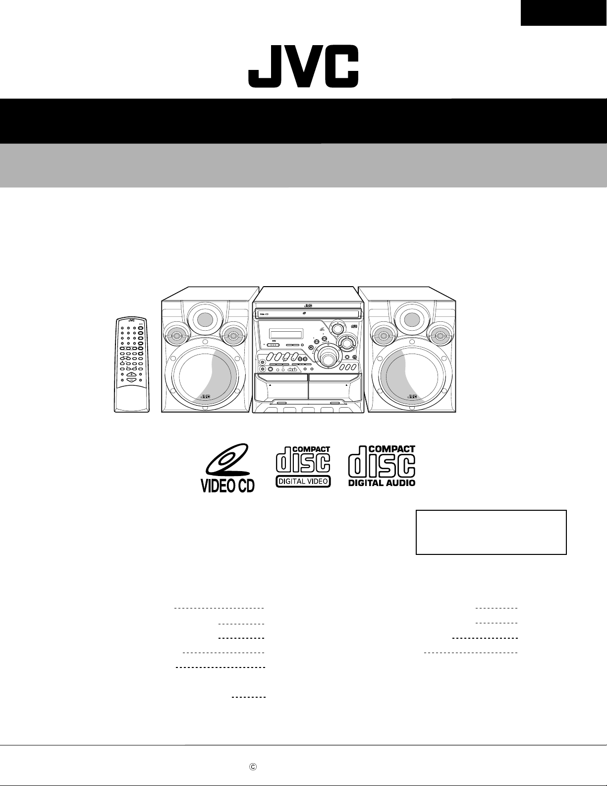
COMPACT COMPONENT SYSTEM
MX-K35V
MX-K35V
RM-SMXK35V REMOTE CONTROL
1 2 3
4 5 6
7 8 9
10 +10
CD1CD2CD3CD
PROGRAM
/RANDOM
KARAOKE
SOUND
MODE
ACTIVE
BASS EX.
Contents
REPEAT TAPE A/B
NEXT V.INTRO HIGHLIGHTPREV.
RETURN STILL
KEY CONTROL
VOLUME
NTSC/PAL
COMPATIBILITY
STANDBY/ON
SLEEP
AUX
FM /AM
FM MODE
SELECT
TAPE
ON SCREEN
MPX
ECHO
FADE
MUTING
COMPACT COMPONENT SYSTEM
STANDBY
PHONES
MIC
STANDBY/ON
X
U
A
REPEAT PROGRAM RANDOM
MIC LEVEL
MAXMIN
EJECT
PLAY
A
3-CD
PLAY & EXCHANGE
MX-K35V
CANCEL SET
E
VCD NUMBER
D
TUNING
P
C
A
T
M/AM
F
SELECT
CD
REC START
/STOP REC START DUBBING
CLOCK
KEY CONTROL
/TIMER
RETURNPBC
FULL - LOGIC CONTROL CD SYNCHRO RECORDING
1 BIT
PREV
TAPE
A/B
CD-R/RW PLAYBACK
DUAL D/A
CONVERTER
ACTIVE
BASS EX.
NEXT
PRESET
E
M
U
L
O
V
P
K
O
C
P
O
R
SOUND
MODE
C
C
L
I
A
S
S
DISC SKIP
CD CONTROL
1
2
3
D
D
D
C
C
C
EJECT
REC/PLAY
B
CA-MXK35VSP-MXK35V SP-MXK35V
Area suffix
US ---------------------- Singapore
UX ------------------- Saudi Arabia
Safety precautions
Preventing static electricity
Important for laser products
Disassembly method
Adjustment method
Flow of functional operation
until TOC read
COPYRIGHT 2001 VICTOR COMPANY OF JAPAN, LTD.
1-2
1-3
1-4
1-5
1-20
1-22
Maintenance of laser pickup
Replacement of laser pickup
Description of major ICs
Wiring connections
1-23
1-23
1-24
1-35
No.21033
Nov. 2001
Page 2
MX-K35V
1. This design of this product contains special hardware and many circuits and components specially for safety
purposes. For continued protection, no changes should be made to the original design unless authorized in
writing by the manufacturer. Replacement parts must be identical to those used in the original circuits. Services
should be performed by qualified personnel only.
2. Alterations of the design or circuitry of the product should not be made. Any design alterations of the product
should not be made. Any design alterations or additions will void the manufacturer`s warranty and will further
relieve the manufacture of responsibility for personal injury or property damage resulting therefrom.
3. Many electrical and mechanical parts in the products have special safety-related characteristics. These
characteristics are often not evident from visual inspection nor can the protection afforded by them necessarily
be obtained by using replacement components rated for higher voltage, wattage, etc. Replacement parts which
have these special safety characteristics are identified in the Parts List of Service Manual. Electrical
components having such features are identified by shading on the schematics and by ( ) on the Parts List in
the Service Manual. The use of a substitute replacement which does not have the same safety characteristics
as the recommended replacement parts shown in the Parts List of Service Manual may create shock, fire, or
other hazards.
4. The leads in the products are routed and dressed with ties, clamps, tubings, barriers and the like to be
separated from live parts, high temperature parts, moving parts and/or sharp edges for the prevention of
electric shock and fire hazard. When service is required, the original lead routing and dress should be
observed, and it should be confirmed that they have been returned to normal, after re-assembling.
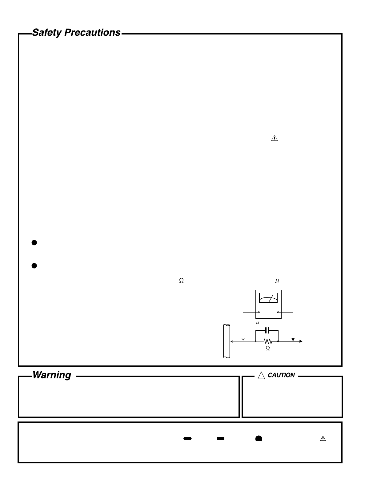
5. Leakage currnet check (Electrical shock hazard testing)
After re-assembling the product, always perform an isolation check on the exposed metal parts of the product
(antenna terminals, knobs, metal cabinet, screw heads, headphone jack, control shafts, etc.) to be sure the
product is safe to operate without danger of electrical shock.
Do not use a line isolation transformer during this check.
Plug the AC line cord directly into the AC outlet. Using a "Leakage Current Tester", measure the leakage
current from each exposed metal parts of the cabinet, particularly any exposed metal part having a return
path to the chassis, to a known good earth ground. Any leakage current must not exceed 0.5mA AC (r.m.s.).
Alternate check method
Plug the AC line cord directly into the AC outlet. Use an AC voltmeter having, 1,000 ohms per volt or more
sensitivity in the following manner. Connect a 1,500 10W resistor paralleled by a 0.15 F AC-type capacitor
between an exposed metal part and a known good earth ground.
Measure the AC voltage across the resistor with the AC
voltmeter.
Move the resistor connection to each exposed metal part,
particularly any exposed metal part having a return path to
the chassis, and meausre the AC voltage across the resistor.
Now, reverse the plug in the AC outlet and repeat each
measurement. Voltage measured any must not exceed 0.75 V
AC (r.m.s.). This corresponds to 0.5 mA AC (r.m.s.).
0.15 F AC TYPE
1500 10W
Good earth ground
AC VOLTMETER
(Having 1000
ohms/volts,
or more sensitivity)
Place this
probe on
each exposed
metal part.
!
1. This equipment has been designed and manufactured to meet international safety standards.
2. It is the legal responsibility of the repairer to ensure that these safety standards are maintained.
3. Repairs must be made in accordance with the relevant safety standards.
4. It is essential that safety critical components are replaced by approved parts.
5. If mains voltage selector is provided, check setting for local voltage.
Burrs formed during molding may
be left over on some parts of the
chassis. Therefore, pay attention to
such burrs in the case of
preforming repair of this system.
In regard with component parts appearing on the silk-screen printed side (parts side) of the PWB diagrams, the
parts that are printed over with black such as the resistor ( ), diode ( ) and ICP ( ) or identified by the " "
mark nearby are critical for safety.
(This regulation does not correspond to J and C version.)
1-2
Page 3
Preventing static electricity
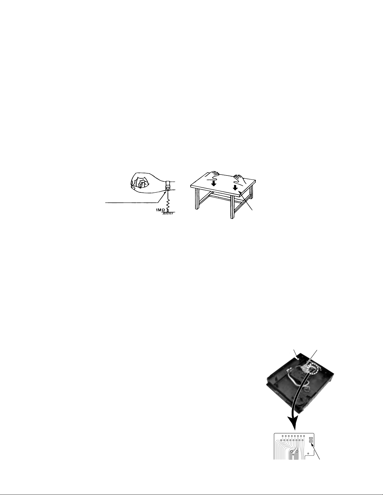
1. Grounding to prevent damage by static electricity
Electrostatic discharge (ESD), which occurs when static electricity stored in the body, fabric, etc. is discharged,
can destroy the laser diode in the traverse unit (optical pickup). Take care to prevent this when performing
repairs.
MX-K35V
2. About the earth processing for the destruction prevention by static electricity
In the equipment which uses optical pick-up (laser diode), optical pick-up is destroyed by the static electricity of
the work environment.
Be careful to use proper grounding in the area where repairs are being performed.
2-1 Ground the workbench
Ground the workbench by laying conductive material (such as a conductive sheet) or an iron plate over
it before placing the traverse unit (optical pickup) on it.
2-2 Ground yourself
Use an anti-static wrist strap to release any static electricity built up in your body.
(caption)
Anti-static wrist strap
Conductive material
(conductive sheet) or iron plate
3. Handling the optical pickup
1. In order to maintain quality during transport and before installation, both sides of the laser diode on the
replacement optical pickup are shorted. After replacement, return the shorted parts to their original condition.
(Refer to the text.)
2. Do not use a tester to check the condition of the laser diode in the optical pickup. The tester's internal power
source can easily destroy the laser diode.
4. Handling the CD changer unit (optical pickup)
1. Do not subject the CD changer unit (optical pickup) to strong shocks, as it is a sensitive, complex unit.
2. Cut off the shorted part of the flexible cable using nippers, etc. after replacing the optical pickup. For specific
details, refer to the replacement procedure in the text. Remove the anti-static pin when replacing the CD
changer unit. Be careful not to take too long a time when attaching it to the connector.
3. Handle the flexible cable carefully as it may break when subjected to strong force.
4. It is not possible to adjust the semi-fixed resistor that adjusts the laser power.
Do not turn it
CD changer
unit
CD changer
mechanism
assembly
Attention when traverse unit is decomposed
*Please refer to "Disassembly method" in the text for pick-up and how to
detach the CD changer mechanism.
1. Remove the CD changer unit.
2. Disconnect the harness from connector on the CD motor board.
3. Solder is put up before the card wire is removed from connector CN601
on the main board as shown in Fig.1 and Fig. 2.
(When the wire is removed without putting up solder, the CD pick-up
assembly might destroy.)
4. Please remove solder after connecting the card wire with CN601 when
you install picking up in the substrate.
Fig.2
Fig.1
Soldering
1-3
Page 4
MX-K35V
Important for laser products
1.CLASS 1 LASER PRODUCT
2.DANGER : Invisible laser radiation when open and inter
lock failed or defeated. Avoid direct exposure to beam.
3.CAUTION : There are no serviceable parts inside the
Laser Unit. Do not disassemble the Laser Unit. Replace
the complete Laser Unit if it malfunctions.
4.CAUTION : The compact disc player uses invisible
laserradiation and is equipped with safety switches
whichprevent emission of radiation when the drawer is
open and the safety interlocks have failed or are de
feated. It is dangerous to defeat the safety switches.
VARNING : Osynlig laserstrålning är denna del är öppnad
och spårren är urkopplad. Betrakta ej strålen.
VARO : Avattaessa ja suojalukitus ohitettaessa olet
alttiina näkymättömälle lasersäteilylle.Älä katso
säteeseen.
5.CAUTION : If safety switches malfunction, the laser is able
to function.
6.CAUTION : Use of controls, adjustments or performance of
procedures other than those specified herein may result in
hazardous radiation exposure.
CAUTION
!
Please use enough caution not to
see the beam directly or touch it
in case of an adjustment or operation
check.
ADVARSEL : Usynlig laserstråling ved åbning , når
sikkerhedsafbrydere er ude af funktion. Undgå
udsættelse for stråling.
ADVARSEL : Usynlig laserstråling ved åpning,når
sikkerhetsbryteren er avslott. unngå utsettelse
for stråling.
REPRODUCTION AND POSITION OF LABELS
WARNING LABEL
DANGER: Invisible laser
radiation when open and
interlock failed or defeated.
AVOID DIRECT EXPOSURE
TO BEAM. (e)
CLASS 1
LASER PRODUCT
ADVARSEL: Usynlig laserstråling ved åbning, når
sikkerhedsafbrydere er ude
af funktion. Undgåudsættelse for stråling (d)
VARNING: Osynlig laserstrålning när denna del är
öppnad och spärren är
urkopplad. Betrakta ej
strålen. (s)
VARO: Avattaessa ja suojalukitus ohitettaessa olet
alttiina näkymättömälle
lasersäteilylle. Älä katso
säteeseen. (f)
1-4
Page 5
MX-K35V
Disassembly method
Commence disassembly of this set by removing the main units and then proceed to the components and
assemblies inside the units.
Replacement of the fuses and the power IC 1-6
Top cover 1-7
CD changer unit 1-8
Front panel assembly 1-9
Chassis unit 1-17
CD changer unit 1-8
Removing the main board 1-10
Removing the CD changer mechanism assembly 1-11
Removing the CD pickup 1-12
Replacing the loading motor and belt of the CD changer tray 1-12
Replacing the CD tray rotor belt of the CD changer, and removing the motor 1-12
Front panel assembly 1-9
Removing the cassette deck mechanism 1-13
Removing the head phone board 1-13
Removing the microphone amplifier board 1-14
Removing the control/FL board 1-14
Removing the switch board and active bass ex. switch board 1-15
Removing the cassette deck main motor, and replacing the main belts 1-16
Removing the leaf switches of the cassette deck mechanism 1-16
Removing the cassette deck heads 1-17
Chassis unit 1-17
Removing the Video & CD board 1-17
Removing the 3-pin regulator 1-18
Removing the power amplifier board, voltage selector board
and power transformer board 1-19
1-5
Page 6
MX-K35V
<Disassembly of the main blocks of this set>
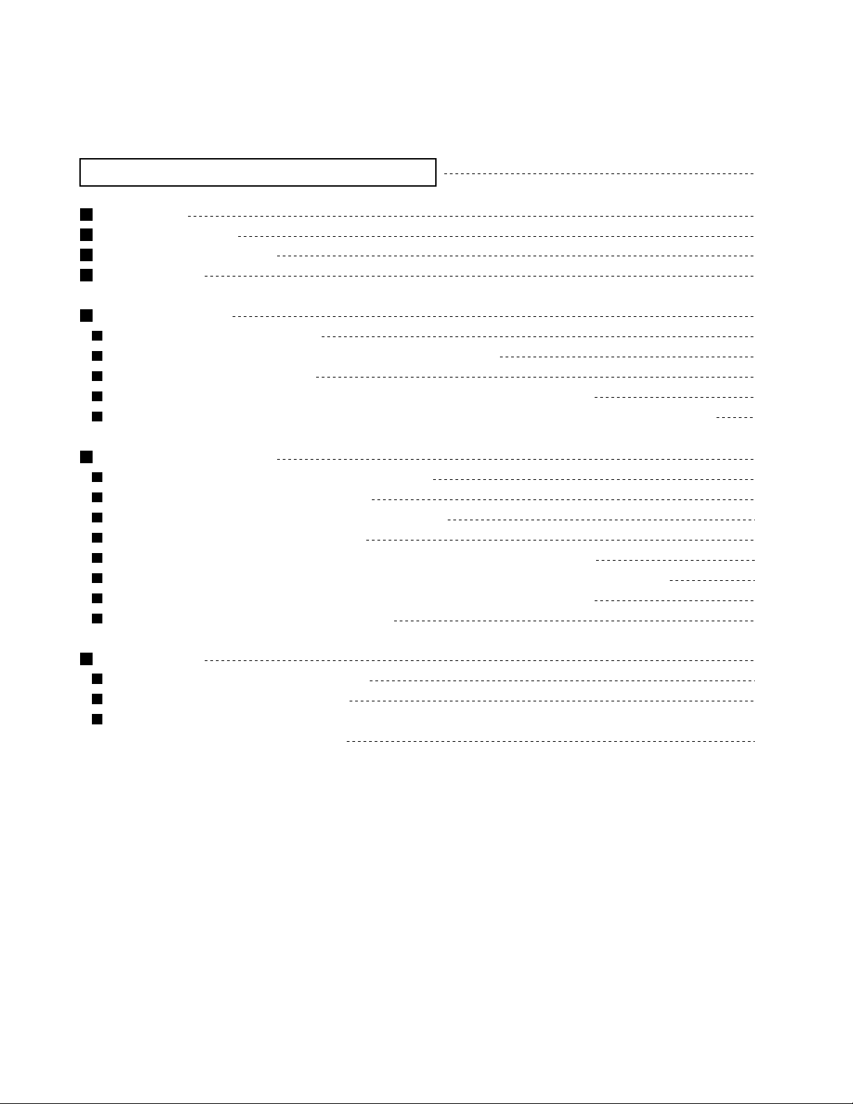
Replacement of the fuses and the power IC
Replacing the fuses (See Fig.1)
Prior to performing the following procedure, remove
the top cover.
1.
Replace the fuses inside.
Fuse (F953)
1.25A 250V
Fuse (F951)
2.5A 250V
Power transformer
board
[Caution] Be sure to use fuses with the specified
ratings.
Replacing the power IC (See Fig.2 to 4)
Prior to performing the following procedure, remove
the top cover.
1.
Remove the two screws A that attach the heat sink
cover to the rear panel.
2.
Pull the heat sink cover outward.
3.
Remove the two screws B from the bracket that
retains the power IC.
4.
Remove the solder fixing the power IC.
Fuse (F952)
1.6A 250V
Chassis
Fig.1
Rear panel
A
Rear panel
B
Heat sink
Heat sink cover
Fig.2
Power amplifier board
Rear
Power IC
soldering part
1-6
Fig.3
Fig.4
Page 7
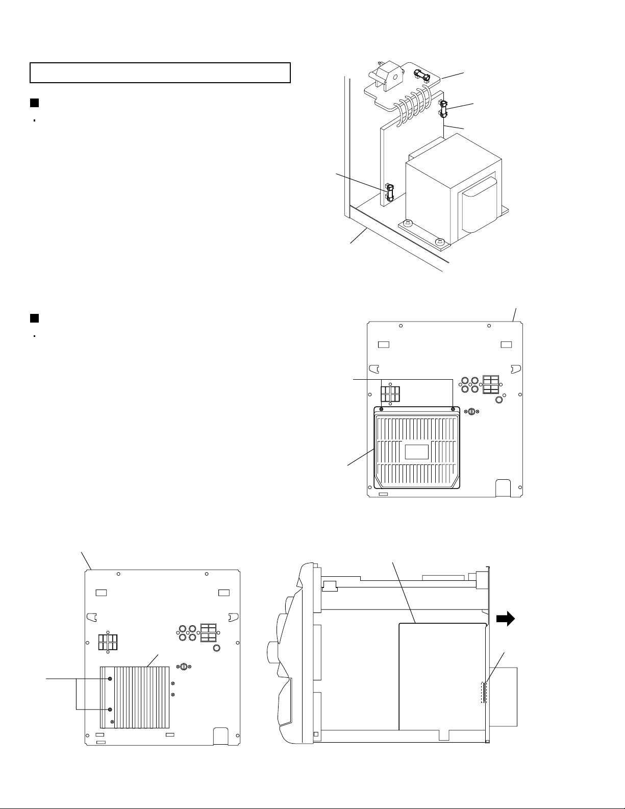
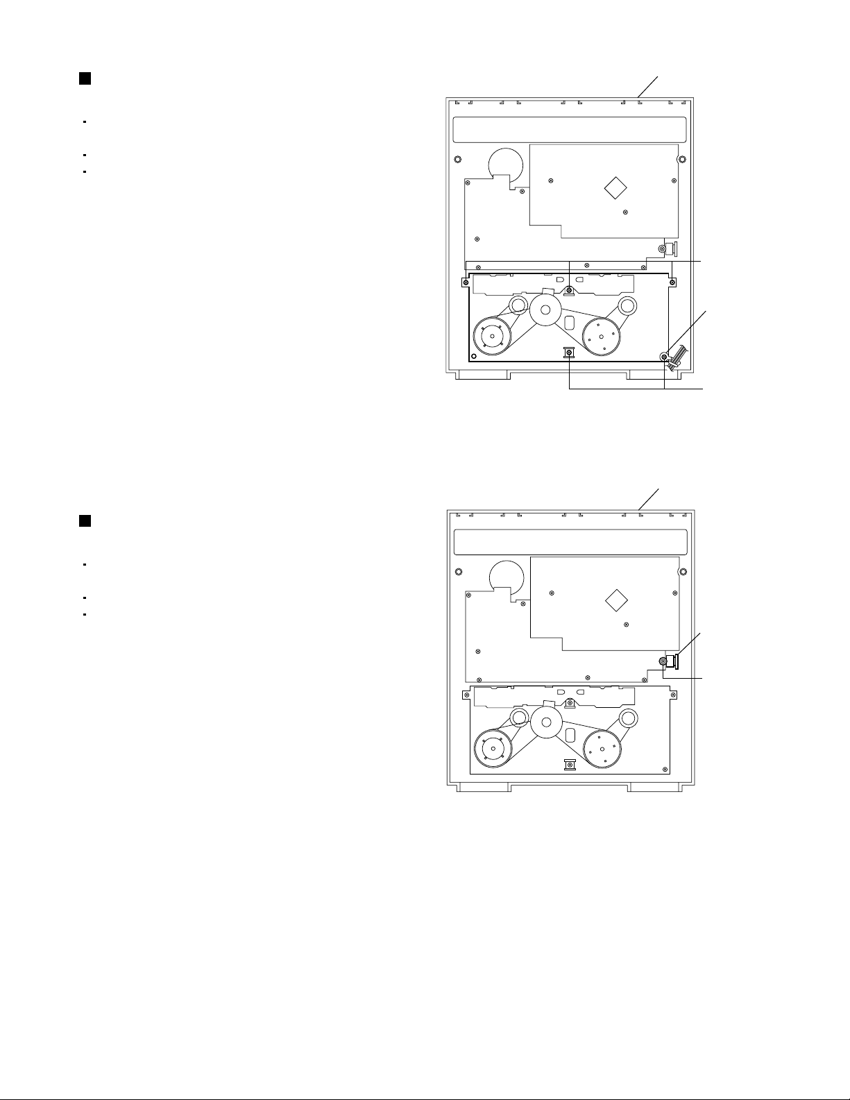
Removing the top cover
(See Fig.5 and 6)
1.
Remove the two screws C and four screws D that
retain the top cover from the rear of the body.
2.
Remove the four screws E retain the top cover from
the two sides of the body.
3.
Remove the top cover from the body by lifting it
toward the rear.
Top cover
MX-K35V
C
DD
Fig.5
Front panel assembly
E
E
Fig.6
1-7
Page 8
MX-K35V
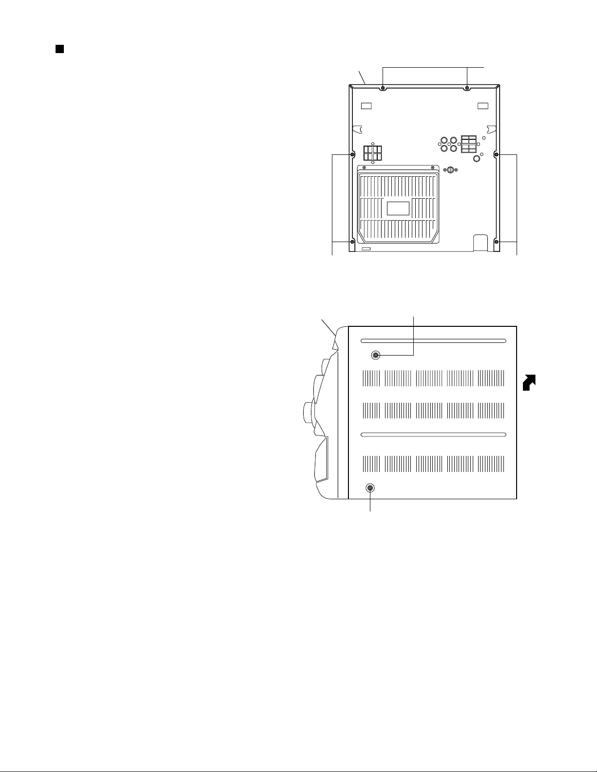
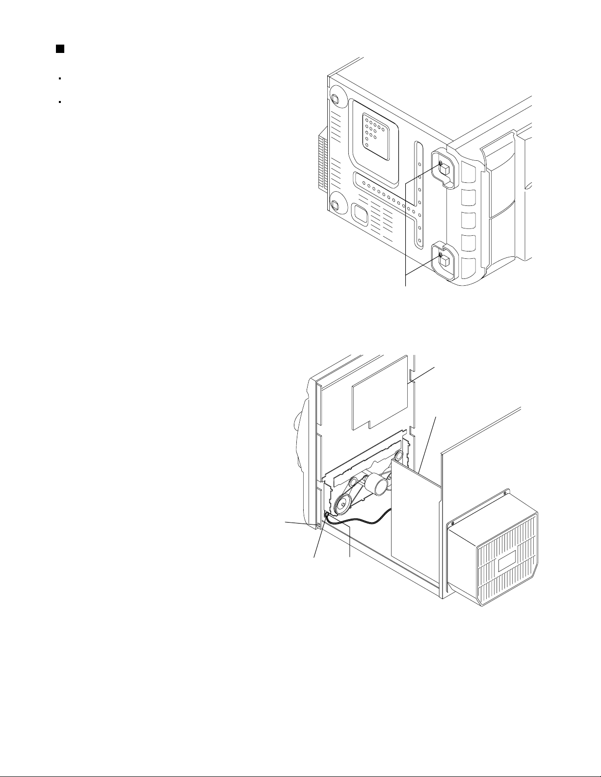
Removing the CD changer unit
(See Fig.7 to 10)
Prior to performing the following procedures,
remove the top cover.
[Caution] Although the CD mechanism unit can be
removed without removing the CD tray
panel, it is still recommended to remove it
in order to prevent damage.
a.
From the front panel side of this set, push in the
sections marked with arrows and pull out the CD
tray toward the front.
b.
Remove the CD tray panel by pushing both of its
extremities upward in the direction of the arrows.
c.
Push the CD tray deep into the set.
1.
Disconnect the cassette head wires from the
connectors CN307 and CN308 on the main board,
which is located below the CD changer unit.
2.
Disconnect the microphone amplifier wire from the
connector CN306 on the main board.
3.
Disconnect the card wires from the connectors
CN301, CN302, CN305 and CN606 on the main
board.
4.
Disconnect the parallel wires from the connectors
CN902A, CN902B and CN902C on the power
amplifier board.
5.
From the rear of the set, remove the two screws F
retaining the CD changer unit, then remove the four
screws G retaining the ANTENNA terminal the
AUX IN terminal and LINE OUT terminal.
6.
Push down and disengage the two claws a holding
the CD changer unit at the bottom of its front panel
and then remove the CD changer unit.(See Fig. 10)
CD tray panel
Fig.7
1-8
AUX IN
terminal
G
Fig.9
F
ANTENNA
terminal
CD tray panel
Fig.8
CD changer
unit
Claw a
Fig.10
Page 9
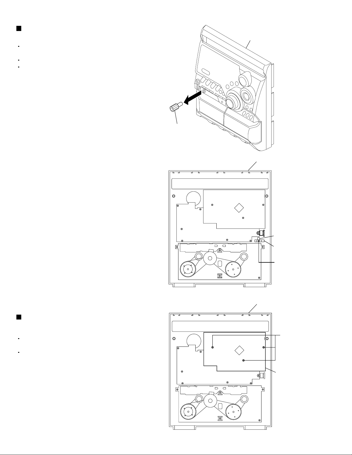
Removing the front panel assembly
(See Fig.11 and 12)
Prior to performing the following procedures,
remove the top cover.
Also remove the CD changer unit.
1.
Disconnect the parallel wire and card wire from the
connectors CN901 and CN903 on the power
amplifier board.
2.
Remove the two screws H retaining the front panel
assembly onto the bottom of the body.
3.
Remove the screw J retaining the cassette deck
mechanism and then remove the GND lug b that
comes from the power amplifier board.
4.
Disengage the claws c on both sides at the bottom
of the front panel assembly and then remove the
assembly.
MX-K35V
H
Fig.11
Claw c
GND lug b
Control/FL board
Power amplifier board
J
Fig.12
1-9
Page 10
MX-K35V
<Disassembly of units and assembly
inside this set>
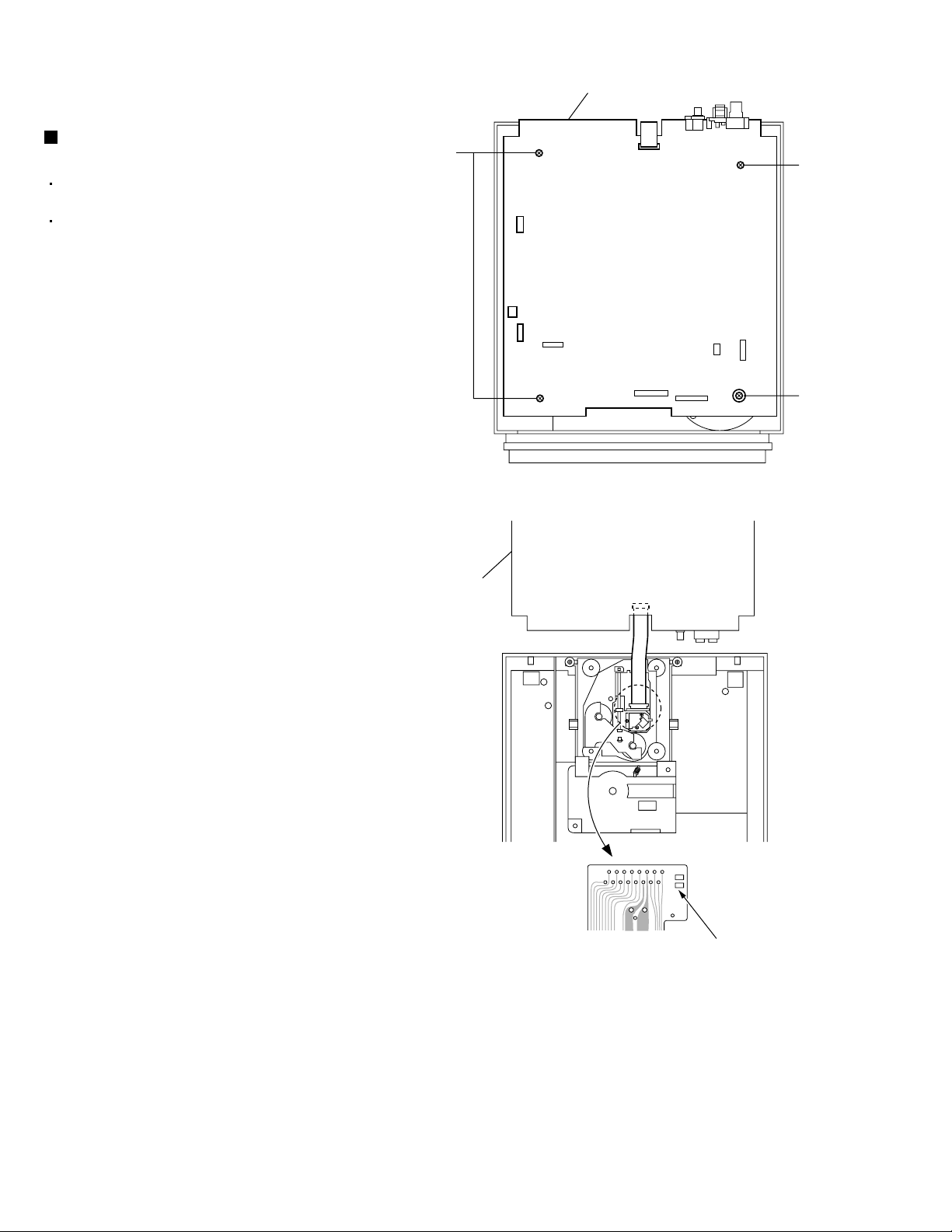
Removing the main board
(See Fig.13 and 14)
Prior to performing the following procedures,
remove the top cover.
Also remove the CD changer unit.
1.
Disconnect the wires from CN602 and CN603 on
the main board, which is located on the backside of
the CD changer unit.
2.
Disconnect the card wire from connector CN604 of
the main board at the back of the CD changer unit.
3.
The three screws K and screw with washer L retain
the main board should be removed.
4.
Remove the main board by pulling it toward the
side where the CN601 is located.
5.
Using solder, short the CD pickup to connect to
short round.
[Caution] (See Fig.14)
After re-connecting the wires, be sure
to remove the shorting solder from the
GND connection.
K
CN604
CN603CN602
Main board
Fig.13
CN601
K
L
6.
Disconnect the card wire from the connector
CN601 on the main board and then remove the
main board.
Main board
CN601
[Caution]
Short round
Fig.14
1-10
Page 11
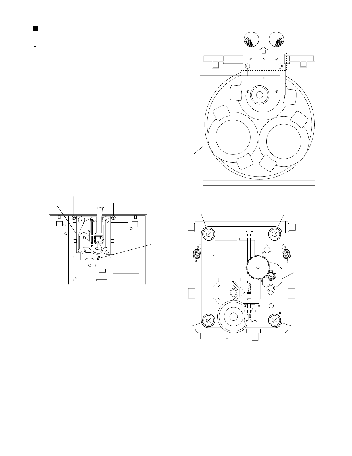
Removing the CD changer mechanism
assembly (See Fig.15 to 17)
Prior to performing the following procedures,
remove the top cover.
Also remove the CD changer unit.
1.
Remove the spring d from the front surface of the
CD changer mechanism unit.
2.
Turn the CD changer mechanism unit upside down,
and remove the spring e connecting the unit to the
CD changer mechanism assembly.
[Note] When re-assembling after the disassembly
work, apply bonding agent on the spring to
prevent it from slipping off.
3.
Remove the two screws with the washer M
retaining the CD changer mechanism assembly.
[Caution] When replacing the CD changer
mechanism assembly, be sure not to
mistake the positions of the red and blue
dampers.
MX-K35V
[Note]
Spring d
CD changer
unit
CD changer
mechanism
assembly
M
Fig.15
Red Red
[Note]
Spring e
CD changer
mechanism
assembly
Fig.16
BlueBlue
Fig.17
1-11
Page 12
MX-K35V
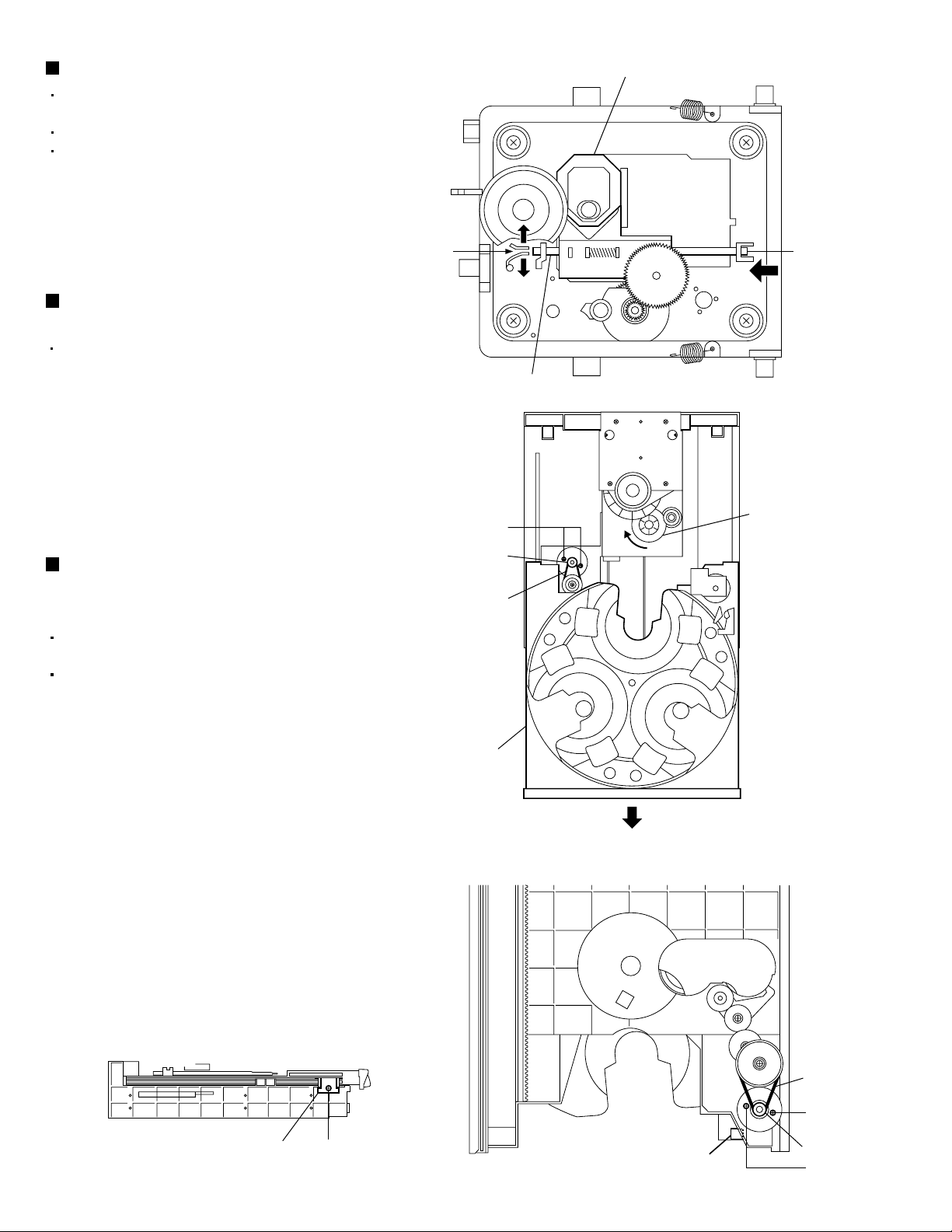
Removing the CD pickup (See Fig.18)
Prior to performing the following procedures,
remove the top cover.
Also remove the CD changer unit.
Also remove the CD changer mechanism
assembly.
1.2.Widen the section f.
While keeping the section f wide open, push the
section g in the direction of the arrow to remove
the shaft, and then remove the CD pickup.
Replacing the loading motor and belt
of the CD changer tray (See Fig.19)
Prior to performing the following procedure,
remove the top cover.
1.
Pull out the CD changer tray.
2.
Remove the belt from the pulley.
3.
Remove the two screws N retaining the CD
changer tray loading motor.
[Caution] When pushing in the CD changer tray, be
sure to lower the CD changer mechanism
assembly by manually turning the UD
cam gear in the direction of the arrow.
Replacing the CD tray rotor belt of the
CD changer, and removing the motor
(See Fig.20 and 21)
N
Pulley
Belt
Shaft
CD pickup
gf
Fig.18
UD cam gear
Prior to performing the following procedures,
remove the top cover.
Also remove the CD changer unit.
1.
Remove the two screws P retaining the stopper
brackets on both sides of the CD changer unit.
2.
Remove the stopper brackets from both sides of
the CD changer unit.
3.
Pull out the CD tray from the CD changer unit, all
the way and then lift the tray upward to remove.
4.
Turn the CD tray upside down and remove the tray
rotor belt from the pulley.
5.
Turn the CD tray upside down and disconnect the
card wire from the connector CN605 on the CD
tray rotor motor assembly.
6.
Remove the two screws Q retaining the CD tray
rotor motor, and then remove the CD tray rotor
motor.
CD changer
tray
Fig.19
CD tray
rotor belt
Q
1-12
Stopper bracket
Fig.20 Fig.21
P
CN605
Pulley
Q
Page 13
Removing the cassette deck mechanism
(See Fig.22)
Prior to performing the following procedure, remove
the top cover.
Also remove the CD changer unit.
Also remove the front panel assembly.
1.Remove the five screws R retaining the cassette
deck mechanism and then remove the wire clamp
lug h that comes from the back of the front panel
assembly.
MX-K35V
Front panel
assembly
R
Wire clamp
lug "h"
R
Fig.22
Removing the head phone board
(See Fig.23)
Prior to performing the following procedure, remove
the top cover
Also remove the CD changer unit.
Also remove the front panel assembly.
Remove the screw with the washer, S that retains
1.
the head phone board from the back of the front
panel assembly.
Front panel
assembly
Head phone
board
S
Fig.23
1-13
Page 14
MX-K35V
Removing the microphone amplifier
board (See Fig.24 and 25)
Prior to performing the following procedure, remove
the top cover
Also remove the CD changer unit.
Also remove the front panel assembly.
Pull out the mic volume knob from the front of the
1.
front panel assembly.
Remove the screw with the washer, T that retains
2.
the microphone amplifier board.
Front panel assembly
Mic volume knob
Fig.24
Front panel
assembly
Removing the control/FL board
(See Fig.26)
Prior to performing the following procedure, remove
the top cover.
Also remove the CD changer unit.
1.Remove the three screws U that retain the
control/FL board from the back of the front panel
assembly.
Braket
Microphone
amplifier board
T
Fig.25
Front panel
assembly
U
Control/FL
board
1-14
Fig.26
Page 15
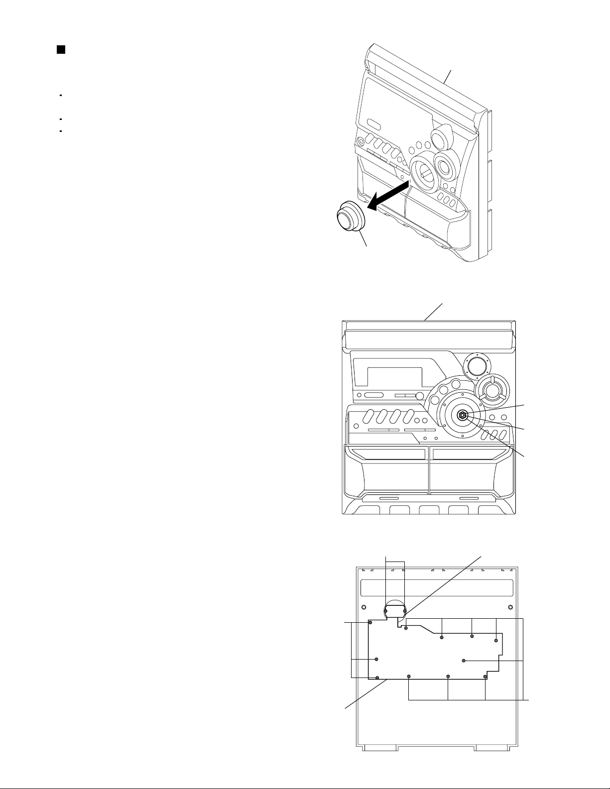
Removing the switch board and active
bass ex. switch board
(See Fig.26 to 29)
Prior to performing the following procedures,
remove the top cover.
Also remove the CD changer unit.
Also remove the front panel assembly.
1.
Pull out the volume control knob from the front of
the front panel assembly.
2.
Remove the nut and washer retaining the volume
knob shaft.
3.
Remove the three screws U retaining the control/FL
board from the back of the front panel assembly.
4.
Remove the control/FL board.
5.
Remove the eleven screws V retaining the switch
board.
6.
Remove the two screws W retaining the active
bass ex. switch board.
MX-K35V
Front panel assembly
Volume knob
Fig.27
Front panel
assembly
V
W
Nut
Volume
shaft
Washer
Fig.28
Active bass ex. switch board
Switch board
Fig.29
V
1-15
Page 16

MX-K35V
Removing the cassette deck main
motor, and replacing the main belts
(See Fig.22, 30 and 31)
Prior to performing the following procedures,
remove the top cover.
Also remove the CD changer unit.
Also remove the front panel assembly.
1.
Remove the five screws R retaining the cassette
deck mechanism.
2.
Remove the cassette deck mechanism.
3.
Remove the two screws X retaining the main motor
from the front side of the cassette deck.
[Caution]
4.
From the backside of the cassette deck, remove
the main motor and two main belts.
After attaching the main motor, check the
orientation of the motor and the polarity of
the wires.
Cassette deck mechanism
(Front side)
Fig.30
Cassette deck mechanism
(Back side)
X
Cassette deck main motor
[Caution]
The lengths of the cassette A (playback
only) and cassette B (record/play) main
belts are different. When attaching the
main belts, use the longer belt for
cassette A.
Removing the leaf switches of the
cassette deck mechanism
(See Fig.22 and 32)
Prior to performing the following procedures,
remove the top cover.
Also remove the CD changer unit.
Also remove the front panel assembly.
1.
Remove the five screws R that retain the cassette
deck mechanism.
2.
Remove the cassette deck mechanism.
3.
Turn the cassette deck mechanism upside down.
4.
Remove the solder from around the leaf switches.
5.
Pull out the leaf switches from the front side of the
cassette deck mechanism.
Main belt
(For B cassette)
Solder side of leaf switch
Cassette deck mechanism
(Back side)
Main belt
(For A cassette)
Fig.31
Fig.32
1-16
Page 17

MX-K35V
Removing the cassette deck heads
(See Fig.22 and 33)
Prior to performing the following procedures,
remove the top cover.
Also remove the CD changer unit.
Also remove the front panel assembly.
1.
Remove the five screws R that retain the cassette
deck mechanism.
2.
Remove the cassette deck mechanism and place it
so that the front side faces up.
3.
Remove the solder from the bottom side of the
head terminal and disconnect the wire.
4.
Remove the screw Y that retains the head.
5.
Loosen the screw Z that retains the head.
6.
Hold the head and slide it in the direction of the
arrow to remove it.
Removing the Video & CD board
(See Fig.2, 34 to 36)
Prior to performing the following procedures,
remove the top cover.
1.
Disconnect the card wire from connector CN606 on
the main board.
2.
Remove the three screws AA and screw AB
retains the Video & CD board cover.
3.
In order to remove the wire from the Video & CD
board, remove the solder on the power amplifier
board.
4.
Remove the Video & CD board cover.
5.
Remove the two screws AC retains the Video & CD
board.
Cassette deck mechanism
(Front side)
PB head REC/PB head
ZY
Fig.33
ZY
AB
Heat sink
AA
Rear
Power amplifier board
Video & CD
board cover
Solder
Fig.35
CN606
Wire
Fig.34
Video & CD board
AC
Fig.36
1-17
Page 18

MX-K35V
Removing the 3-pin regulator
(See Fig.2, 37 and 38)
Prior to performing the following procedures,
remove the top cover.
1.
Remove the two screws A connecting the heat sink
cover to the rear panel.
2.
Pull the heat sink cover foward you.
3.
Remove the screw AD that retains the bracket
holding the 3-pin terminal regulator.
4.
Remove the solder fixing the 3-pin regulator.
Rear panel
Heat sink
AD
Fig.37
Power amplifier board
Fig.38
Rear
Solder on the
3-pin regulator
1-18
Page 19

MX-K35V
Removing the power amplifier board,
voltage selector board and power
transformer board
(See Fig.2, 3, 37, 39 to 42)
Prior to performing the following procedures,
remove the top cover.
Also remove the CD changer unit.
1.
Remove the two screws A connecting the heat
sink cover to the rear panel.
2.
Pull out the heat sink cover toward you.
3.
Remove the two screws B that retain the bracket
supporting the power IC.
4.
Remove the screw AC that retain the bracket
holding the 3-pin terminal regulator.
5.
Remove the two screws AE that retain the
SPEAKERS terminals.
6.
Remove the screw AF that retains the rear panel,
and then remove the rear panel.
7.
Remove the two screws AG that retain the voltage
selector board.
8.
Disconnect the parallel wires from the connectors
CN951A and CN951B on the power amplifier
board.
9.
Remove the screw AH that retain the power
amplifier board and then remove the assembly.
10.
Remove the solders j connecting the six wires.
11.
Remove the four screws AJ that retain the power
transformer board and then remove the assembly.
Rear panel
Speaker
terminal
AE
AG
Voltage
selector
AF
Fig.39
Rear panel
Power amplifier board
CN951B
CN951A
Power amplifier board
Chassis
AH
Voltage selector
board
AJ
Chassis
(Top view)
j
Fig.40
Chassis
Power transformer
board
AJ
j
Clamp
AC power cord
Fig.41
Fig.42
1-19
Page 20

MX-K35V
Adjustment method
Measurement instruments required
for adjustment
1. Low frequency oscillator,
This oscillator should have a capacity to output 0dB
to 600ohm at an oscillation frequency of 50Hz-20kHz.
2. Attenuator impedance : 600ohm
3. Electronic voltmeter
4. Frequency counter
5. Wow flutter meter
6. Test tape
VT712 : For Tape speed and wow flutter ( 3kHz)
VT703 : For Head angle(10kHz),Play back frequency
VT724 : For reference signal test(1kHz)
VT739 : For frequency response test(63Hz,1kHz,10kHz)
7. Blank tape
TAPE : AC-225, TAPE : AC-514
8. Torque gauge : For play and back tension
Forward ; TW2111A, Reverse ; TW2121A
Fast Forward and Rewind ; TW2231A
9. Test disc
: CTS-1000(12cm),GRG-1211(8cm)
10. Jitter meter
Radio input signal
AM modulation frequency : 400Hz
Modulation factor : 30%
FM modulation frequency : 400Hz
Frequency displacement : 22.5kHz
Frequency Range
AM 522kHz~1629kHz (at 9kHz channel space)
FM 87.5MHz~108MHz
Standard measurement positions of volume
and switch
Power : Standby (Light STANDBY Indicator)
A.BUSS switch: OFF
Sound mode : OFF
Main VOL. maximum
Travers mecha set position : Disc 1
Mic MIX VOL : MAX
ECHO : OFF
Measurement conditions
Power supply voltage
AC110/127/220/230-240V (50Hz/60Hz) : US/UX
Measurement
output terminal : Speaker out
: TP101(Measuring for TUNER/DECK/CD)
: Dummy load 6ohm
Precautions for measurement
1. Apply 30pF and 33kohm to the IF sweeper output
side and 0.082 F and 100kohm in series to
the sweeper input side.
2. The IF sweeper output level should be made as
low as possible within the adjustable range.
3. Since the IF sweeper is a fixed device, there is
no need to adjust this sweeper.
4. Since a ceramic oscillator is used, there is no need
to perform any MPX adjustment.
5. Since a fixed coil is used, there is no need to adjust
the FM tracking.
6. The input and output earth systems are separated.
In case of simultaneously measuring the voltage
in both of the input and output systems with an
electronic voltmeter for two channels, therefore,
the earth should be connected particularly.
7. In the case of BTL connection amplifier, the minus
terminal of speaker is not for earthing. Therefore,
be sure not to connect any other earth terminal
to this terminal. This system is of an OTL system.
1-20
Page 21

Arrangement of adjusting positions
Cassette deck mechanism
(Front side)
PB Head
(Deck-A)
REC/PB Head
(Deck-B)
MX-K35V
Main board
CN308
8-Pin
L301
FM VT voltage
measurement point
Head azimuth screw
(Forward side)
Head screw Head screw
Head azimuth screw
Tape recorder section
Items
Cassette Head
Azimuth Alignments
Recording Bias
Frequency Alignment
Measurement
conditions
Test tape
: VT703 (10kHz)
Measurement output
terminal
: Headphone Output
(32-ohm loaded)
or
Left and Right
speaker output
(6-ohm loaded)
Recording tape
: TYPE AC-514
Measurement output
terminal
: Erase head terminal
(CN308 8-Pin)
(Forward side)
1. Playback the test tape VT703 (10KHz) or equivalent.
2. Adjust the head azimuth screw to obtain maximum
output and both output of L / R is in 3dB.
3. Put on the screw lock paint after alignments.
1. Insert the recording tape in deck-B.
2. Starting the recording.
3. Adjust the oscillation frequency to 80KHz+/-3KHz by
core of Oscillation coil of L301.
Antenna coil
Measurement method
AM VT voltage
measurement point
R6
R3
L2
T1
OSC coil
Standard
values
Maximum output
Adjusting
positions
Head azimuth
screw
Adjust the head
azimuth screw only
when the head has
been changed.
80kHz+/-3kHz
Bias coil: L301
Use the HighImpedance Probe for
Frequency counter
input.
Tuner section
Items
AM Tracking
Alignments
AM IFT Alignments
Note: The adjustment of CD section is not required.
Measurement
conditions
Input signal
: 530kHz
Measurement point
: Resistor R3 (AM)
Resistor R6 (FM)
Input signal
: 603kHz
Input signal
: 531kHz
OSC coil adjustment
1.Set the Signal Generator signal to 530KHz the feed to
Loop Antenna.
2.Receiving the signal and the adjust the OSC coil (L2)
obtain the V.T is 1.40V +/-0.05V.
Antenna coil check or adjustment
1.Change the receiving frequency to 603KHz.
2.Adjust the Antenna coil ( L2 ) obtain maximum sensitivity.
(Adjust the SSG output to out of AGC range.)
1. Set the receiving frequency to 531KHz.
2. Feed the 450KHz signal to AM IF input.
3.Adjust the IFT Block T1 obtain to maximum output.
(Adjust the SSG output to out of AGC range.)
Measurement method
Standard
values
V. T
: 1.40V+/-0.05V
Maximum
sensitivity
Maximum output
Adjusting
positions
OSC/Antenna coil
: L2
Adjust the OSC coil
only when the AM coil
block has been
changed.
IFT (T1)
Adjust the IFT only
when the IFT block has
been changed.
1-21
Page 22

MX-K35V
Flow of functional operation until TOC read
Power ON
Play Key
Slider turns REST
SW ON.
Automatic tuning
of TE offset
Check Point
Confirm that the voltage at the pin1
of CN602 is "H"\"L"\"H".
Tracking error waveform at TOC reading
pin 14 of
IC601(TEO)
Approx
1.8V
VREF
Disc states
to rotate
Approx.3sec
Tracking
servo
off states
Automatic measurement
of TE amplitude and
automatic tuning of
TE balance
Tracking
servo
on states
Disc to be
braked to stop
TOC reading
finishes
500mv/div
2ms/div
Fig.1
Laser ON
Detection of disc
Automatic tuning of
Focus offset
Automatic measurement of
Focus S-curve amplitude
Disc is rotated
Focus servo ON
(Tracking servo ON)
Automatic measurement of
Tracking error amplitude
Automatic tuning of
Tracking error balance
Check that the voltage at the
pin9 of IC601 is + 5V?
Confirm that the Focus error
S-cuve signal at the pin 16 of
IC601 is approx.2Vp-p
Confirm the waveform of
the Tracking error signal.
at the pin 14 of IC601 (R617)
(See fig-1)
1-22
Automatic tuning of
Focus error balance
Automatic tuning of
Focus error gain
Automatic tuning of
Tracking error gain
TOC reading
Play a disc
Confirm the eys-pattern
at the lead of RFO
Page 23

MX-K35V
Maintenance of laser pickup
(1) Cleaning the pick up lens
Before you replace the pick up, please try to
clean the lens with a alcohol soaked cotton
swab.
(2) Life of the laser diode
When the life of the laser diode has expired,
the following symptoms will appear.
1. The level of RF output (EFM output:ampli
tude of eye pattern) will below.
Is the level of
RFOUT under
1.25V 0.22Vp-p?
YES
O.K
NO
Replace it.
Replacement of laser pickup
Turn off the power switch and,disconnect the
power cord from the AC OUTLET.
Replace the pickup with a normal one.(Refer
to "Removing the CD pickup" on the previous page)
Plug the power cord in,and turn the power on.
At this time,check that the laser emits for
about 3seconds and the objective lens moves
up and down.
Note: Do not observe the laser beam directly.
Play a disc.
Check the eye-pattern.
Finish.
(3) Semi-fixed resistor on the APC PC board
The semi-fixed resistor on the APC printed circuit board which is
attached to the pickup is used to adjust the laser power.Since this adjustment should be performed to match the
characteristics of the whole optical block, do not touch the semi-fixed resistor.
If the laser power is lower than the specified value,the laser diode is almost worn out, and the laser pickup should
be replaced.
If the semi-fixed resistor would be adjusted when the pickup operates normally,the laser pickup may be damaged
due to excessive current.
1-23
Page 24

MX-K35V
Description of major ICs
TMP87CM78 (IC701) : System control microprocessor
1. Terminal layout
80 51
50
100 81
2. Pin function
1
VDD
2
3
4
5
6
7
8
9
10
11
12
13
14
15
16
17
18
19
20
21
22
23
24
25
26
27
28
29
30
31
32
33
34
35
36
37
AB
BIAS
RPHD
BC1
uRTS
uDA
uCLK
MPX
PER
SD
SCK
REM
KEY0
KEY1
KEY2
VER
LV L
SFTY
TPA
TPB
VSS
VASS
VAREF
VDD
INH
TEST
XTI
XTO
VSS
XIN
XOUT
RST
uSTB
PRT
FCD
FTU
31
30
1
+5V back up supply
Deck A/B select control
O
Recording bias on/off control
O
Deck-B head switch control
O
Bias frequency control
O
MPEG RTS input
I
MPEG serial data I/O
I/O
MPEG serial clock input
I
FM stereo indicator input
I
PLL periode output
O
PLL serial data I/O
I/O
PLL serial clock output
O
IR remote signal input
I
Key-0 ADC input
I
Key-1 ADC input
I
Key-2 ADC input
I
Version set
I
Level meter input
I
Safety input
I
Deck-A switch matrix input
I
Deck-B switch matrix input
I
Digita ground
I
ADC reference ground
ADC reference +5V supply
+5V back up supply
INH bit input
I
Test mode / ground
I
32.768kHz X'Tal iput
I
32.768kHz X'Tal output
O
Digita ground
-
8.0MHz X'Tal
I
8.0MHz X'Tal
O
Reset circuit
I
MPEG strobe input
I
Protector input
I
CD power supply control
O
Tuner power supply control
O
38
39
40
41
42
43
44
45
46
47
48
49
50
80
81
82
83
84
85
86
87
88
89
90
91
92
93
94
95
96
97
98
99
100
63
79
Symbol I /OPin No. Symbol I/ O Function
PCNT
SHFT
SMUT
SPK
LMUT
ECHO
AHB
KARA
VCK
VDAT
VOL+
VOL-
VKK
G13
P16
DOP
DCL
Reservd
CLS
CW
CCW
CNTT
OPSW
CLSW
UPSW
DWSW
DCNT
TPSW
OPN
DETA
DETB
MOT
SOLB
SOLA
PBM
RECM
G1
P1
System power on/off control
O
Clock shift output
O
System mute cotrol output
O
Speaker mute control output
O
Line output mute control
O
Echo on/off control output
O
Active bass boost control output
O
Karaoke mode on/off control
O
Sound processor serial clock out
O
Sound processor serial data out
O
Volume up jog signal input
I
Volume down jog signal input
I
-35V supply
VFD grid output
O
VFD plate output
O
MPEG door open
O
MPEG door close
O
Reserved
Tray close control output
O
Turn table CW output
O
Turn table CCW output
O
Turn table speed control
O
Tray open detect switch input
I
Tray close detect switch input
I
Pickup up detect switch input
I
Pickup down detect switch input
I
Disc count switch input
I
Turn table position SW input
I
Tray open control output
O
Tape-A real rotation detector
I
Tape-B real rotation detector
I
Motor on/off control
O
Deck-B solenoide control
O
Deck-A solenoide control
O
Tape playback muting control
O
Recording mute control
O
Pin No. Function
51
64
1-24
Page 25

ES3880FL (IC101) : MPEG decoder
MX-K35V
1. Terminal layout
80 ~ 51
100 ~ 81
1 ~ 30
3. Pin function
Pin No.
Symbol I/O Function
1
VDD
2
RAS#
3
DWE#
4~12
13~28
32~39
45~49
55~62
68~79
29
30
31
40
41
42
43
44
50
51
52
53
54
63
64
65
66
67
80
81
DA0~8
DBUS0~15
RESET#
VSS
VDD
YUV0~7
VSYNC
HSYNC
CPUCLK
PCLK2X
PCLK
AUX0~4
VSS
VDD
AUX6
AUX5
AUX7
LD0~7
LWR#
LOE#
LCS3#
LCS1#
LCS0#
LA0~11
VSS
VPP
2. Block diagram
Processor
Interface
31 ~ 50
Serial
Audio
Interface
TDM
Interface
3.3V power supply
Row address strobe
O
DRAM write enable
O
DRAM multiplexed row and column address bus
O
DRAM data bus
I/O
System reset
I
Ground
-
3.3V power supply
YUV[7:0] 8-bit video data bus
O
Vertical sync
I/O
Horizontal sync
I/O
RISC and system clock input. CPUCLK is used
I
only if SEL_PLL[1:0] = 00 to bypass PLL.
Doubled 54MHz pixel clock
I/O
27MHz pixel clock
I/O
Auxiliary control pins 4:0
I/O
AUX0 and AUX1 are open collectors.
Ground
-
3.3V power supply
Auxiliary control pins 6
I/O
Auxiliary control pins 5
I/O
Auxiliary control pins 7
I/O
RISC interface data bus
I/O
RISC interface write enable
O
RISC interface output enable
O
RISC interface chip select
O
RISC interface chip select
O
RISC interface chip select
O
RISC interface address bus
O
Ground
-
5.0V power supply
-
LA[17:0]
LD[7:0]
LCS3#, LCS#[1:0]
LWR#
LOE#
ACLK
ATCLK
AIN
AOUT
ARFS
ATFS
ARCLK
SEL_PLL[1:0]
TDMCLK
TDMDR
TDMFS
RISC
Processor
Serial Audio
Interface
TDM
Interface
Pin No.
82~87
88
89
90
91
92
93
94
95
96
97
98
99
100
Huffman
Decoder
64x32 ROM
32x32 SRAM
Symbol I/O
LA12~17
ACLK
AOUT
SEL_PLL0
ATCLK
ATFS
SEL_PLL1
DA9
DOE#
AIN
ARCLK
ARFS
TDMCLK
TDMDR
TDMFS
CAS#
VSS
DRAM Interface
2Kx32 ROM
512x32 SRAM
MPEG
Processor
Registers
DRAM DMA
Controller
Video Output
On Screen
Display
Function
RISC interface address bus
O
Master clock for external audio DAC
I/O
Audio interface serial data output when
O
selected.
System and DSCK output clock
I
frequency selection at reset time. The
matrix below lists the available clock
frequencies and their respective PLL
bit settings.
SEL_PLL1 SEL_PLL0 DCLK
0 0 Bypass PLL (input mode)
0 1 54MHz (output mode)Default
1 0 67.5MHz (output mode)
1 1 81.0MHz (output mode)
Audio transmit bit clock
I/O
Audio transmit frame sync
O
Refer to the description and matrix for
I
SEL_PLL0 pin 89.
DRAM multiplexed row and column
O
address line 9
DRAM output enable
O
Audio serial data input
I
Audio receive bit clock
I
Audio receive frame sync
I
TDM serial clock
I
TDM serial data receive
I
TDM frame sync
I
DRAM column address strobe
O
Ground
-
RAS#
DA[9:0]
DBUS[15:0]
DOE#
DWE#
CAS#
AUX[7:0]
YUV[7:0]
PCLK2X
PCLK
VSYNC
HSYNC
CPUCLK
RESET#
DRAM
AUX
Screen
Display
Misc.
1-25
Page 26

MX-K35V
ES3883F (IC102) : Companion chip
1. Terminal layout
80 ~ 51
100 ~ 81
2. Pin function
1
5
6
7
8
9
RESET_B
AUX7/NFD_DI
AUX8/NFD_CLK
SPLL_OUT
AUX9/SQSO
SEL_PLL1
RSTOUT_B
SEL_PLL0
AUX10/SQCK
AUX11/IRQ
AUX12/C2PO
AUX14/SOSI
VSS
NC
VCC
DSC_C
AUX0
DSC_D0
AUX1
DSC_S
AUX2
DCLK
EXT_CLK
MUTE
VCC
MCLK
TWS
TSD
TBCK
RWS
VSS
NC
VSS
VCC
RSD
RBCK
SER_IN
AUX13/SP
AUX15/IR
VSSAA
VCM
VREFP
2~4
10
11
12
13
14
15
16
17
18
19
20
21
22
23
24
25,26
27~30
31
32
33
34
35
36
37
38
39
40
41
42
43
31 ~ 50
1 ~ 30
Ground
No connect
Voltage supply, 5V
Clock for programming to access internal
I
registers
Servo forward or general-purpose I/O
I/O
Data for programming to access internal
I/O
registers
Servo reverse or general-purpose I/O
I/O
Strobe for programming to access internal
I
registers
Servo LDON or general-purpose I/O
I/O
DCLK is the MPEG decoder clock.
O
EXT_CLK is the external clock.
I
EXT_CLK is an input during bypass PLL mode.
Video reset (active-low)
I
I/O
Servo BRKM/sense or general-purpose I/O / VFD_DI
O
Audio mute
-
Voltage supply, 5V
I
Audio master clock
I/O
Servo mute/open or general-purpose I/O / VFD_CLK
I
TWS is the transmit audio frame sync.
O
SPLL_OUT is the select PLL output.
I/O
Servo SQSO or general-purpose I/O
I
Transmit audio data input
I
Transmit audio bit clock
O
RWS is the receive audio frame sync.
I
SEL_PLL[1:0] select the PLL clock frequency for
the DCLK output.
SEL_PLL1 SEL_PLL0 DCLK
0 0 Bypass PLL (input mode)
0 1 27MHz (output mode)
1 0 32.4MHz (output mode)
1 1 40.5MHz (output mode)
O
Reset output (active-low)
-
Ground
-
No connect
-
Ground
-
Voltage supply, 5V
O
RSD is the receive audio data input.
I
SEL_PLL0 and SEL_PLL1 select the PLL clock
frequency for the DCLK output. Refer to the
table in the definition for pin 23.
I/O
Servo SQCK or general-purpose I/O
I/O
ES3880 IRQ or interrupt output or general-purpose I/O
I/O
CD C2PO or interrupt input or general-purpose I/O
O
RBCK is the receive audio bit clock.
I
SER_IN is the serial input DSC mode:
0 = Parallel DSC mode
1 = Serial DSC mode
I/O
Serial interrupt/CD-mute or general-purpose I/O
I/O
Servo SCOR (SOSI), interrupt input,
or general-purpose I/O
I/O
Interrupt input or general-purpose I/O
-
Audio analog ground
I
ADC common mode reference (CMR) buffer output.
CMR is approximately 2.25V. Bypass to analog ground
with 47uF electrolytic in paralell with 0.1uF.
I
DAC and ADC maximum reference. Bypass to video
CMR (VCMR) with 10uF in parallel with 0.1uF.
44
49
50
51
52
Symbol I/OPin No. Symbol I/O Function
VCCAA
AOR+,AOR-
AOL-,AOL+
MIC1
MIC2
VSSAA
VREF
Analog VCC, 5V
I
Right channel output
O
Left channel output
O
Microphone input 1
I
Microphone input 2
I
Audio analog ground
Internal resister divider generates CMR
I
Pin No. Function
45,46
47,48
voltage.
Bypass to analog ground with 0.1uF.
DAC and ADC minimum reference.
53
VREFM
I
Bypass to VCMR with 10uF in parallel
with 0.1uF.
Full-scale DAC current adjustment
54
55
56,57
58
59,60
61
RSET
COMP
VSSAV
CDAC
VCCAV
YDAC
I
Compensation pin
I
Video analog ground
Modulated chrominance output
O
Video VCC, 5V
Y luminance data bus for screen video
O
port
Video analog ground
62,63
64
65
66
67
68
69
70
71
72
73
74
75
76
77
78
79
80
81
VSSAV
VDAC
ACAP
VCC
AUX6/VFD_DO
AUX5
AUX4
AUX3
XOUT
VSS
VCC
XIN
VSS
NC
VSS
VCC
PCLK
2XPCLK
DSC_D7
Composite video output
O
Audio CAP
I
Voltage supply, 5V
Servo XLAT or general-purpose I/O / VFD_DO
I/O
Servo data or general-purpose I/O
I/O
Servo CCW/close or general-purpose I/O
I/O
Servo CW/limit or general-purpose I/O
I/O
Crystal output
O
Ground
Voltage supply, 5V
27MHz crystal input
I
Ground
No connect
Ground
Voltage supply, 5V
-
13.5MHz pixel clock
I/O
27MHz(2 times pixel clock)
I/O
Data for programming to access internal
I/O
registers
Horizontal sync (active-low)
82
83
HSYNC_B
DSC_D6
O
Data for programming to access internal
I/O
registers
Vertical sync (active-low)
84
85
VSYNC_B
DSC_D5
O
Data for programming to access internal
I/O
registers
YUV data bus for screen video port
86~89
90
91
92
93
YUV7~4
VCC
VSS
YUV3
DSC_D4
I
Voltage supply, 5V
Ground
YUV data bus for screen video port
I
Data for programming to access internal
I/O
registers
YUV data bus for screen video port
94
95
YUV2
DSC_D3
I
Data for programming to access internal
I/O
registers
YUV data bus for screen video port
96
97
YUV1
DSC_D2
I
Data for programming to access internal
I/O
registers
YUV data bus for screen video port
98
99
YUV0
DSC_D1
I
Data for programming to access internal
I/O
registers
Ground
100
VSS
-
1-26
Page 27

BA15218 / BA15218F (IC102 / IC852) : Dual operational amplifier
1. Terminal layout & block diagram
MX-K35V
OUT1 1
-IN1 2
8 Vcc
7 OUT2
1
+IN1 3
6 -IN2
2
G 4
5 +IN2
BA3837 (IC103) : MIC Mixer
1. Terminal layout & block diagram
VCC
1
MIC
LOUT
FK
TK
LIN
BIAS
GND
+
2
-
-
3
4
5
6
7
8
+
SW2
SW1
L-R
L
+
-
+
-
+
L+R
LOGIC
+
+
-
R
+
2. Pin function
10
11
12
13
14
15
16
Symbol
VCC
1
2
LOUT
3
4
5
6
BIAS
7
GND
8
9
ROUT
MIC
FK
TK
LIN
RIN
LP
LP
LP
A
B
C
I/O
Power supply
Microphone mixing input
I
Channel L output
O
Non connect
Non connect
Channel L input
I
Signal bias
I
Connect to GND
Channel R input
I
Connects to LPF time constant element
O
Connects to LPF time constant element
O
LPF outpout
O
Channel R output
O
Mode select input A
I
Mode select input B
I
Mode select input C
I
C
16
B
15
A
14
ROUT
13
12
LP
11
LP
LP
10
9
RIN
Pin No.
Function
BU9253FS (IC851) : Low pass filter & echo mixer
2. Pin function1. Terminal layout & block diagram
GND
ECHO VR
BIAS
DAINTO
DAINTI
DALPFI
DALPFO
MIXO
Pin No.
16
A/D
- +
15
14
13
12
11
10
9
CR
MUTE
VCC
ADINTI
ADINTO
ADLPFO
ADLPFI
MIXI
1
2
3
4
D/A
5
6
- +
7
8
MIX
OSC
COUNTER
SRAM
1
2
3
4
5
6
7
8
9
10
11
12
13
14
15
16
Symbol
GND
ECHO VR
BIAS
DAINTO
DAINTI
DALPFI
DALPFO
MIXO
MIXI
ADLPFI
ADLPFO
ADINTO
ADINTI
VCC
MUTE
CR
I/O
Connect GND
Echo level control
I
Analog part DC bias
DA side integrator output
O
DA side integrator intput
I
DA side LPF input
I
DA side LPF output
O
Mix AMP output for original tone& echo tone
O
Mix AMP input pin for original tone
I
AD side LPF input
I
AD side LPF output
O
AD side integrator output
O
AD side integrator input
I
Power supply
Mute control signal input
I
CR pin for oscillator
-
Function
1-27
Page 28

MX-K35V
PST9119 (IC703) : Reset IC
1. Terminal layout 2. Block diagram
1
OUT
2
VDD
3
VSS
123
STK402-070 (IC151) : 2-ch audio power amplifier
1. Terminal layout 2. Block diagram
PRE-VCC
VDD
OUT
VSS
VCC
IN 1
NF 1
SUB G
TA2092N (IC603) : Power driver IC for CD
1. Terminal layout
Block diagram
&
1
PWGND
2
OUT(-)1
3
PVCC1
4
OUT(+)1
5
VIN1
6
VRI
7
VCI
8
VIN2
9
OUT(+)2
10
PVCC2
11
OUT(-)2
12
PWGND
24
23
22
21
20
19
18
17
16
15
14
13
PWGND
OUT(-)4
PVCC4
OUT(+)4
VIN4
SVCC
SGND
VIN3
OUT(+)3
PVCC3
OUT(-)3
PWGND
2. Pin function
PIN
Symbol
PWGND
OUT(-)1
PVCC1
OUT(+)1
VIN1
VRI
VCI
VIN2
OUT(+)2
PVCC2
OUT(-)2
PWGND
I/O
-
O
-
O
I
I
O
I
O
-
O
-
No.
1
2
3
4
5
6
7
8
9
10
11
12
Power ground
Inverted output for CH1
Supply terminal of output stage for CH1
Non-inverted output for CH1
Input for CH1
Input reference voltage
Output reference voltage
Input for CH2
Non-inverted output for CH2
Supply terminal of output stage for CH2
Inverted output for CH2
Power ground
BIAS
PRE-VSS
Function
OUT 1-
OUT 1+
OUT 2-
OUT 2+
PIN
No.
13
14
15
16
17
18
19
20
21
22
23
24
Symbol
PWGND
OUT(-)3
PVCC3
OUT(+)3
VIN3
SGND
SVCC
VIN4
OUT(+)4
PVCC4
OUT(-)4
PWGND
VSS
IN 2
NF 2
I/O
Power ground
Inverted output for CH3
O
Supply terminal of output stage for CH3
Non-inverted output for CH3
O
Input for CH3
I
Supply terminal of small signal ground
Small signal ground
Input for CH4
I
Non-inverted output for CH4
O
Supply terminal of output stage for CH4
Inverted output for CH4
O
Power ground
-
Function
1-28
Page 29

TA2153FN (IC601) : RF amplifier for digital servo
1. Terminal layout
2. Block diagram
MX-K35V
1
VCC
FNI
FPI
TPI
TNI
MDI
LDO
SEL
TEB
2VRO
TEN
TEO
SBAD
2
3
4
5
6
7
8
9
10
11
12
13
14
15
RFAGC
GMAD
3. Pin function
PIN No.
Symbol
1
VCC
2
RFAGC
3
GMAD
4
FNI
5
FPI
6
TPI
7
TNI
8
MDI
9
LDO
10
SEL
30
RFN2
29
GND
28
RFO
27
AGCIN
26
GVSW
25
RFGO
24
RFRPIN
23
PKC
22
RFCT
21
STC
20
RFRP
19
VRO
18
SEB
17
FEN
16
FEO
I/O
Power supply input terminal
RF amplitude adjustment control signal input terminal. Controlled by 3-PWM signals. (PWM carrier = 88.2kHz)
I
Open loop gain adjustment terminal for AGC amplifier
I
Main beam I-V amplifier input terminal
I
Main beam I-V amplifier input terminal
I
Sub beam I-V amplifier input terminal
I
Sub beam I-V amplifier input terminal
I
Monitor photo diode amplifier input terminal
I
Laser diode amplifier input terminal
O
Laser diode control signal input terminal and APC circuit ON/OFF control sugnal terminal
I
RFN229GND28RFO27AGCIN26GVSW25RFGO24RFRPIN23PKC22RFCT21STC20RFRP19VRO18SEB17FEM16FEO
30
+
AGC Amp.
+
+
-
+
-
I-I
1
2
3
4
5
FPI6TPI
RFAGC
GMAD
FNI
VCC
PEAK
BOTTOM
+
-
I-I
7
TNI
+
-
+
-
-
+
-
+
-
SW3
-
+
SW2
DET.
3 STATE
SW1
8
9
10
11
MDI
SEL
TEB
LDO
+
+
12
-
2VRO
+
-
+
-
+
13
14
TEN
TEO
Function
+
15
-
SBAD
SEL level APC circuit LDO Detect frequency
GND OFF Connected to Vcc through resistor (1kohm) Low
Hiz ON Control signal output Low
Vcc ON Control signal output High
11
12
13
14
15
16
17
18
19
20
21
22
23
24
25
26
27
28
29
30
TEB
2VRO
TEN
TEO
SBAD
FEO
FEN
SEB
VRO
RFRP
STC
RFCT
PKC
RFRPIN
RFGO
GVSW
AGCIN
RFO
GND
RFN2
I
Tracking error balance adjustment signal input terminal. Controlled by 3-PWM signals. (PWM carrier = 88.2kHz)
O
Reference voltage (2VRO) output terminal 2RVO = 4.2V when Vcc = 5V
I
TE amplifier negative input terminal
O
TE error signal output terminal
O
Sub beam adder signal output terminal
O
Focus error signal output terminal
I
FE amplifier negative input terminal
I
RFRP output circuit switching terminal
SEL level Bottom detection Peak detection
GND ON ON
Vcc OFF ON
O
Reference signal (VRO) output terminal
O
Track count signal output terminal
I
Time constant adjustment terminal for bottom detection
O
RFRP signal center level output terminal
I
Time constant adjustment terminal for peak detection
I
Input terminal for track count signal output amplifier
O
Output terminal for RF signal amplitude adjustment amplifier
I
Amplifier (AGC, FE, TE) gain switching terminal
GVSW Mode
GND CD-RW
Hiz Normal
Vcc Normal
I
Input terminal for RF signal amplitude adjustment amplifier
O
Output terminal RF signal amplifier
-
Ground terminal
I
Input terminal for RF signal amplifier
1-29
Page 30

MX-K35V
TA8189 (IC401) : REC/PB amplifier
1. Terminal layout 2. Block diagram
NF1
EQ1
GND
1
24
23
22
21
20
19
18
17
16
15
14
13
CH2_A
CH2_B
NF2
EQ2
PREOUT2
A/B_SW
VCC
CG
REC_OUT2
REC_NF2
REC_IN2
ALC
2
3
4
5
6
7
8
9
10
11
12
23CH2_B
24CH2_A
1CH1_A
2CH1_B
CH1_A
CH1_B
PREOUT1
MIX_OUT
GND1
EQSW
REC_OUT1
REC_NF1
REC_IN1
3. Pin function
Pin
No.
Symbol
I/O
1 CH1_A I Input for playback amp. (Ch1): A cassette
(PB)
2 CH1_B I Input for playback amp. (Ch1): B cassette
(REC/PB)
3 NF1 I NF terminal for playback amp.
4 EQ1 O Metal output for playback amp.
5 PREOUT1 O Output terminal for playback amp.
6 MIX_OUT O Mixing output
7 GND1 - Ground
8 EQSW I Metal/Normal mode select switch
REC_OUT1
9
O Output for recording amp.
10 REC_NF1 I NF terminal for recording amp.
11 REC_IN1 I Input for recording amp.
12 GND1 - Ground terminal
Function
NF2
22
3 54 6 7 8
NF1
Ch2
+
+
Ch1
-
Pin
No.
EQ2
EQ1
PREOUT2
2021 19
PREOUT1
Symbol
A/B_SW
A/B
ref1
V
MIX_OUT
18
VCC
ref
I
GND1
I/O
13 ALC I ALC filter terminal
14 REC_IN2 I Input for recording amp.
15 REC_NF2 I NF terminal for recording amp.
16
REC_OUT2
O Output for recording amp.
17 CG O Charge detection terminal
18 VCC - Power supply terminal
19 A/B_SW I REC amp. Select switch (A cassette/B
20 PREOUT2 O Output terminal for playback amp.
21 EQ2 O Metal output for playback amp.
22 NF2 I NF terminal for playback amp.
23 CH2_B I Input for playback amp. (Ch2): B cassette
24 CH2_A I Input for playback amp. (Ch2): A cassette
CG
17
ref2
V
M/N
EQSW
cassette)
(REC/PB)
(PB)
REC_OUT2
16
9
REC_OUT1
Ch2
Ch1
REC_NF2
15
-
+
+
-
10
14 REC_IN2
13 ALC
ALC
12 GND
11 REC_IN1
REC_NF1
Function
TA8409S (IC604, IC605) : Motor driver
1. Terminal layout 2. Truth table
IN1
123456789
VS
OUT1
VR
IN1
1-30
IN2
VCC
OUT2
NC
GND
INPUT OUTPUT MODE
IN2
OUT1
0
0
1
0
0
1
1
1
OUT2
H
L
L
L
H
L
MOTOR
STOP
CW/CCW
CCW/CW
BRAKE
Page 31

TA2104N (IC1) : 1chip AM/FM, MPX tuner system
1. Terminal layout 2. Pin function
RFGND
FM_RFIN
AM_FIL
MIX_OUT
VCC
AM_IFIN
FM_IFIN
GND
AGC
QUAD
R_OUT
L_OUT
10
11
12
PIN
Symbol
1
2
3
4
5
6
7
8
9
24
FM_RFOUT
23
RFVCC
22
AM_RFIN
21
FM_OSC
20
AM_OSC
19
OSC_OUT
18
ST_IND
17
IF_REQ
16
DET_OUT
15
MPX_IN
14
LPF2/M_ST
13
LPF1/BAND
No.
1
2
3
4
5
6
7
8
9
10
11
RFGND
FM_RFIN
AM_FIL
MIX_OUT
AM_IFIN
FM_IFIN
R_OUT
12
VCC
GND
AGC
QUAD
L_OUT
I/O
I
I
O
I
I
I
I
O
O
Function
Ground terminal for RF
Input of FMRF signal
AM low frequency cut
Output of FM/AM RF mix
Power supply terminal
Input of AMIF signal
Input of FMIF signal
Ground terminal
AGC voltage input terminal
OSC terminal for FM DET.
Output R-channel
Output L-channel
TC9257P (IC2) : PLL frequency synthesizer
1. Terminal layout
1
XT
2
XT
DATA
OT-1
OT-2
OT-3
OT-4
3
4
5
6
7
8
9
10
PERIOD
CLOCK
I/O-5 / CLK
20
DO2
19
DO1
18
I/O-7
17
I/O-8 / NF1
16
I/O-9 / NF2
15
GND
14
FMIN
13
AMIN
12
VDD
11
I/O-6
2. Pin function
PIN
Symbol
No.
1
XT
2
XT
3
PERIOD
4
CLOCK
5
DATA
6
OT-1
7
OT-2
8
OT-3
9
OT-4
10
I/O-5/CLK
11
I/O-6
12
VDD
I/O
Crystal oscillator pins
I
Crystal oscillator pins
O
Period signal input
I
Clock signal input
I
Serial data input/output
I/O
General-purpose output port
O
General-purpose output port
O
General-purpose output port
O
General-purpose output port
O
General-purpose I/O port
I/O
General-purpose I/O port
I/O
Power supply pin
-
PIN
Symbol I/O Function
No.
13
LPF1/BAND
14
LPF2/M_ST
15
MPX_IN
16
DET_OUT
17
IF_REQ
18
ST_IND
19
OSC_OUT
20
AM_OSC
21
FM_OSC
22
AM_RFIN
23
RFVCC
24
FM_RFOUT
Function Function
PIN
No.
13
14
15
16
I
FM/AM switch
I
Stereo/monoral switch
I
Multiplex signal input
O
AM/FM detection output
O
IF out/REQ out
O
Stereo indicator output
O
PLL data bus for FM or AM
-
AM local oscillation circuit
-
FM local oscillation circuit
I
Input of AMRF signal
-
Power supply teminal for RF
O
Output of FMRF signal
Symbol I/O
AMIN
FMIN
GND
I/O-9
I/O
NF2
Programmable counter input
I
Programmable counter input
I
Ground pin
-
General-purpose I/O port
General-purpose counter frequency
I
measurement input
17
I/O-8
NF1
General-purpose I/O port
I/O
General-purpose counter frequency
I
measurement input
18
19
20
I/O-7
DO1
DO2
General-purpose I/O port
I/O
Phase comparator output
O
Phase comparator output
O
MX-K35V
3. Block diagram
AMP
FMIN
14
AMIN
13
XT
2
XT
1
DATA
5
CLOCK
4
PERIOD
3
FM
L
1/2
FMHHF
OSC
CIRCUIT
2 MODULUS
PRESCALER
FM MODE LF
OSC
1ms
ADDRESS
DECODER
OUTPUT PORT
OT-1
OT-2
PSC
4bit SWALLOW
COUNTER
12bit PROGRAMMABLE COUNTER
4
REFERENCE COUNTER
24bit REGISTER
24bit SHIFT REGISTER
4
TEST
24bit REGISTER
4 4
UNIVERSAL COUNTER CONTROL
OT-4
9876
OT-3
OT-4
POWER ON
RESET
12
15
24 22
20bit BINARY COUNTER
XT
5
10
1ms
VDD
12
MAX
4
RESET
PHASE
COMPARATOR
UNLOCK
5
GATE
GND
15
TRI-STATE
BUFFER
TRI-STATE
BUFFER
OT4
I/O PORT
AMP
AMP
19
20
10
11
16
17
18
DO1
DO2
I/O-5/CLK
I/O-6
I/O-9/NF2
I/O-8/NF1
I/O-7
1-31
Page 32

MX-K35V
TC9462F (IC602) : Digital servo single chip processor
1. Terminal layout
80 51
50
100 81
2. Pin function
1
TEST0
2
HSO
3
UHSO
4
EMPH
5
LRCK
6
VSS
7
BCK
8
AOUT
9
DOUT
10
MBOV
11
12
13
14
15
16
17
18
19
20
21
22
IPF
SBOK
CLCK
VDD
VSS
DATA
SFSY
SBSY
SPCK
SPDA
COFS
MONIT
31
30
1
Pin No. Function
Test mode terminal. Normally, keep at open
I
Playback speed mode flag output terminal.
O
UHSO HSO PLAYBACK SPEED
O
23
24
H H Normal
H L 2 times
L H 4 times
L L -
Subcode Q data emphasis flag output terminal.
O
25
26
27
28
Emphasis ON at "H" level and OFF at "L" level.
The output polarity can invert by command.
Channel clock output terminal. (44.1kHz)
O
L-ch at "L" level and R-ch at "H" level. The
29
30
output polarity can invert by command.
Digital ground terminal.
Bit clock output terminal. (1.4112MHz)
O
Audio data output terminal.
O
Digital data output terminal.
O
Buffer memory over signal output terminal.
O
Over at "H" level.
Correction flag output terminal.
O
At "H" level, AOUT output is made to correction
impossibility by C
O
Subcode Q data CRCC check adjusting result
2
correction processing.
output terminal. The adjusting result is OK at
"H" level.
I/O
Subcode P
W data readout clock input/output
terminal. This terminal can select by command
bit.
-
Digital power supply voltage terminal.
-
Digital ground terminal.
O
Subcode P
O
Playback frame sync signal output terminal.
O
Subcode block sync signal output terminal.
O
Processor status signal readout clock output
W data output terminal.
31
32
33
34
35
36
37
38
39
40
41
42
43
44
45
terminal.
O
Processor status signal output terminal.
O
Correction frame clock output terminal.
(7.35kHz)
O
Internal signal (DSP internal flag and PLL
clock) output terminal. Selected by command.
This terminal output the text data with serial
46
47
48
49
50
by command.
Symbol I /OPin No. Symbol I / O Function
VDD
TESIO0
P2VREF
HSSW
ZDET
PDO
TMAXS
TMAX
LPFN
LPFO
PVREF
VCOREF
VCOF
AVSS
SLCO
RFI
AVDD
REFCT
RFZI
RFRP
FEI
SBAD
TSIN
TEI
TEZI
FDO
TRO
VREF
Digital power supply voltage terminal.
Test input/output terminal. Normally, keep at
I
"L" level. The terminal that inputted the clock
for read of text data by command.
PLL double reference voltage supply terminal.
2/4 times speed at "V
O
O
1 bit DA converter zero detect flag output
REF
" voltage.
terminal.
Phase difference signal output terminal of
O
EFM signal and PLCK signal.
TMAX detection result output terminal.
O
Selected by command bit (TMPS).
TMAX detection result output terminal.
O
Selected by command bit (TMPS).
DIFFERENCE RESULT TMAX OUTPUT
Longer than fixed freq. "P2V
REF
"
Shorter than fixed freq. "Vss"
Within the fixed freq. "HiZ"
LPF amplifier inverting input terminal for PLL.
I
LPF amplifier output terminal for PLL.
O
PLL reference voltage supply terminal.
VCO center frequency reference level terminal.
I
Normally, keep at "PV
O
VCO filter terminal.
-
Analog ground terminal.
O
Data slice level output terminal.
I
RF signal input terminal.
-
Analog power supply voltage terminal.
I
RFRP signal center level input terminal.
I
RFRP zero cross input terminal.
I
RF ripple signal input terminal.
I
Focus error signal input terminal.
I
Sub-beam adder signal input terminal.
I
Test input terminal. Normally, keep at "V
REF
" level.
REF
"
level.
I
Tracking error signal input terminal.
Take in at tracking servo on.
I
Tracking error zero cross input terminal.
O
Focus servo equalizer output terminal.
O
Tracking servo equalizer output terminal.
-
Analog reference voltage supply terminal.
1-32
Page 33

MX-K35V
51
52
53
54
55
56
57
58
59
60
61
62
63
64
65
66
67
68
69
70
RFGC
TEBC
FMO
FVO
DMO
2VREF
SEL
FLGA
FLGB
FLGC
FLGD
VDD
VSS
IO0
IO1
IO2
IO3
DMOUT
CKSE
DACT
71
72
73
74
75
76
77
78
79
80
81
82
83
84
85
86
87
88
89
90
91
92
93
94
95
96
97
98
99
100
Symbol I /OPin No. Symbol I / O Function
TESIN
TESIO1
VSS
PXI
PXO
VDD
XVSS
XI
XO
XVDD
DVSR
RO
DVDD
DVR
LO
DVSL
TEST1
TEST2
TEST3
BUS0
BUS1
BUS2
BUS3
VDD
VSS
BUCK
CCE
TEST4
TSMOD
RST
Pin No. Function
RF amplitude adjustment control signal output
O
terminal.
Tracking balance control signal output terminal.
O
Feed equalizer output terminal.
O
Speed error signal or feed search equlizer
O
output terminal.
Disk equalizer output terminal. (PWM carrier=
O
88.2kHz for DSP, Synchronize to PXO)
Analog double reference voltage supply
terminal.
APC circuit ON/OFF indication signal output
O
terminal. At the laser on time, UHF = L at "HiZ"
level and UHF = H at "H" level.
Extermal flag output terminal for internal
O
signal. Can select signal from TEZC, FOON,
FOK and RFZC by command.
Extermal flag output terminal for internal
O
signal. Can select signal from DFCT, FOON,
FMON and RFZC by command.
Extermal flag output terminal for internal
O
signal. Can select signal from TRON, TRSR,
FOK and SRCH by command.
Extermal flag output terminal for internal
O
signal. Can select signal from TRON, DMON,
HYS and SHC by command.
Digital power supply voltage terminal.
Digital ground terminal.
General I/O terminal. Can change over input
I/O
port or output port by command. At the input
I/O
mode time can readout a state of terminal (H/L)
I/O
by read command. At the output mode time can
I/O
control a state of terminal (H/L/HiZ) by
command.
This terminal controls IO0
I
At "L" level time, IO0, 1 out feed equalizer
signal of 2-state PWM, IO2,3 out disk equalizer
signal of 2-state PWM.
I
Normally, keep at open.
I
DAC test mode terminal. Normally, keep at
open.
IO3 terminal.
Test input terminal. Normally, keep at "L" level.
I
Test input/output terminal. Normally, keep at
I
"L" level.
Digital ground terminal.
Crystal oscillator connecting input terminal for
I
DSP. Normally, keep at "L" level.
Crystal oscillator connecting output terminal
O
for DSP.
Digital power supply voltage terminal.
Oscillator ground terminal for system clock.
Crystal oscillator connecting input terminal for
I
system clock.
Crystal oscillator connecting output terminal
O
for system clock.
Oscillator power supply voltage terminal for
system clock.
Analog ground terminal for DA converter.(R-ch)
R channel data forward output terminal.
O
Analog supply voltage terminal for DA
converter.
Reference voltage terminal for DA converter.
L channel data forward output terminal.
O
Analog ground terminal for DA converter.(L-ch)
Test mode terminal. Normal, keep at open.
I
Test mode terminal. Normal, keep at open.
I
Test mode terminal. Normal, keep at open.
I
Micon interface data input/output terminal.
I/O
I/O
I/O
I/O
Digital power supply voltage terminal.
Digital ground terminal.
Micon interface clock input terminal.
I
Command and data sending/receiving chip
I
enable signal input terminal.
The bus line becomes active at "L" level.
Test mode terminal. Normal, keep at open.
I
Local test mode selection terminal.
I
Reset signal input terminal. Reset at "L" level.
I
1-33
Page 34

MX-K35V
TDA7440D (IC101) : Audio processor
1. Terminal layout 2. Block diagram
4
RIN3
RIN2
RIN1
MUXO-L
IN(L)
MUXO-R
IN(R)
BIN(R)
BOUT(R)
BIN(L)
1
2
3
4
LIN1
5
LIN2 VS
LIN3
6
7
LIN4
8
9
10
11
12
13
14
28
RIN4
27
LOUT
26
ROUT
25
AGND
24
CREF
23
SDA
22
SCL
21
DGND
20
TRE(R)
19
18
TRE(L)
17
PS1
16
LP
15
BOUT(L)
LIN1
LIN2
LIN3
LIN4
RIN1
RIN2
RIN3
RIN4
5
6
7
3
2
1
28
4C16256 (IC103) : 4MB EDO-RAM
1. Terminal layout
2. Pin function
100K
100K
100K
100K
100K
100K
100K
100K
G
0/30dB
2dB STEP
G
INPUT MULTIPLEXER
+ GAIN
BASS
BASS
R
B
R
B
BOUT(L)
BOUT(R)BIN(R)
MUXO-L IN(L)
8 9 18 14 15
VOLUME
VOLUME
10 11 19 12 13 23
MUXO-R IN(R)
TRE(L)
BIN(L)
TREBLE
I2CBUS DECODER + LATCHES
TREBLE
TRE(R)
SPKR ATT
LEFT
SPKR ATT
RIGHT
V
REF
SUPPLY
CREF
27
LOUT
21
SCL
22
SDA
20
DGND
26
ROUT
24
VS
25
AGND
1
VCC
VCC
NC
NC
WE
RAS
NC
VCC
2
D0
3
D1
4
D2
5
D3
6
7
D4
8
D5
9
D6
10
D7
11
12
13
14
15
16
A0
17
A1
18
A2
19
A3
20
GND
40
D15
39
D14
38
37
D13
D12
36
GND
35
34
D11
D10
33
32
D9
D8
31
NC
30
CASL
29
CASH
28
OE
27
A8
26
A7
25
24
A6
23
A5
22
A4
21
GND
27C020 (IC104) : 2MB PROM
1. Terminal layout
1
VPP
A16
A15
A12
GND
2
3
4
5
A7
6
A6
7
A5
8
A4
9
A3
10
A2
11
A1
12
A0
13
D0
14
D1
15
D2
16
VCC
32
PGM
31
A17
30
A14
29
A13
28
27
A8
26
A9
A11
25
OE
24
A10
23
CE
22
D7
21
D6
20
19
D5
D4
18
D3
17
PIN No. Symbol Function
1,6,20
2~5,7~10,
VCC
D0~D15
I/O
Power supply terminal
Data input/output
I/O
31~34,36~39
11,12,15,30
13
14
16~19,22~26
21,35,40
27
28
29
NC
WE
RAS
A0~A8
GND
OE
CASH
CASL
Not used
Write enable terminal
I
Row address strobe terminal
I
Address input
I
Ground teminal
Output enable terminal
I
Upper column address strobe terminal
I
Lower column address strobe terminal
I
2. Pin function
PIN No. Symbol Function
1
2~12
13~15
16
17~21
22
23
24
25~30
31
32
VPP
A16,A15,A12,A7~A0
D0~D2
GND
D3~D7
CE
A10
OE
A11,A9,A8,A13,A14,A17
PGM
VCC
I/O
Power supply terminal
Address input
I
Data input/output
I/O
Ground terminal
Data input/output
I/O
Chip enable terminal
I
Address input
I
Output enable teminal
I
Address input
I
Program strobe
I
Power supply terminal
-
1-34
Page 35

Wiring connections
Color codes are shown below.
1Brown
2 Red
3 Orange
4 Yellow
5 Green
6 Blue
7 Violet
8Gray
9 White
0Black
Microphone
amplifier board
FW852
1
3-5305-028-01-07
3-5316-010-01-07
Spindle motor
Cassette deck
main motor
Cassette mechanism
Cassette board
P.B. head bottom sideA REC/P.B. head bottom sideB
3-5315-017-01-07
L2
0 29
1
+
-
+
3-5400-594-01-00
Card wire
1
-
912 4 9 6 2
CN306
MX-K35V
Control/FL board
Card wire
CN703
1
3-5322-018-01-07
Card wire
A
3-5400-595-01-00
0
2
0
9
2
90
1
CN308
L301
CN307
CN302
0
2
94
6
1
Parallel wire
CN702
1
FW702-2
1
1
CN701
1
1
FW701
FW701
FL tube
3-5309-020-02-07
CD
B
C1117
pickup
Feed motor
Video & CD board
CN1101
1
3-5325-030-01-07
Card wire
AC
input
6
1
TB901
Voltage selector board
0
1
TB902
TRANS
Power transformer board
6
2
3
4
1
FW951
1
CD pickup unit
6
4
3-5400-569-01-00
1
B
A
3-5309-019-01-07
CN601
FW1051
IC151
1
6
4
1
CN602
Card wire
Head phone board
POWER IC
Power amplifier board
1
J31
CN903
CN951B
CN951A
1
CN901
Parallel wire
1
0
CASS.
GND
T1
1
3-5304-037-01-07
CN902A
CN902B
CN902C
Main board
1
CN606
1
CN303
1
CN604
1
Card wire
3-5311-019-01-07
3-5305-030-01-07
Turn table
motor
Turn table
motor board
CN603
9
9/2
1
CN301
CN305
1
1
9
9/69/4
9/0
Table pos.
board
W608
1
Tray motor
18
3-5400-538-01-00
9/2
W608
W607
CN605
1
3-5322-018-01-07
Active bass ex.
switch board
3-5400-593-01-00
9
9/2
+
81
1
1
W607
Switch board
3-5302-010-01-07
1
FW702-1
3-5311-027-01-07
9/0
9/4
9
1
1
W603
W606
Pickup switch
board
3-5303-018-01-07
Parallel wire
3-5302-012-02-07
1
1
W606
Tray switch
board
Disc count board
9/29/6
1-35
Page 36

Block diagrams
Main
Deck-A
5
4
3
2
PB-Head
To
Deck-B
R/P-Head
To
Cassette
Mechanism
To
CD Pickup
To
Spindle
Sleed
CN307
CN308
CN305
CN601
CN602
Control/FL
VFD
Q303
Bias OSC
Q309~314
Mech
Control
IC601
TA2153F
CD RF Amp
IC603
TA2092N
4CH Driver
IC701
TMP87CK78-XXX
CN702
To Main To Main
Q401,501
Rec Mute
To Power Amp
CN701
MPU
IC401
TA8189N
Tape PB/Rec
Q402,502
PB Mute
IC602
TC9462F
Digital Servo
CN703
CN606
To MPEG
FW701
Switch
IR Sensor
FW701
TC9257P
IC702
Jog
Key's
IC2
PLL
CN604
To Changer
FM/AM Ant.
JA302
IC1
TA2104N
AM/FM-MPX
Tuner
IC605
TA8409S
Motor Driver
IC604
TA8409S
Motor Driver
CN603
To Changer
To
Main
JA301
AUX In
Tuner
Tape
VCD
CN1101
4C16256
4MB EDO-RAM
AUX
CD
IC1101
ES3880FL
MPEG
Decorder
IC1103
To Mic/Echo
CN306
IC103
BA3837
V.Cancel
IC101
TDA7440D
Vol,Tone,
Selector
IC1102
ES3883
Companion
Chip
IC1104
27C020
2MB PROM
JA303
Line-Out
Q101
AHB
IC102
BA15218
AHB
Q201
AHB
IC1105
AMS1117
3.3V Reg
To
Power Amp
CN303
To
Control
CN301
To
Control
CN302
J1101
Video Output
To
Main
To
Control
To
Main
Mic Jack
To
Power Amp
Power amplifier
Q151
Mute
CN901
Q251
Mute
Protect.
Control
Circuit
CN902
Power supply
Transformer
FW951
Selector
ECHO
JA851
Q851
ALC
Head phone
FW1051
T951
Voltage
J1053
2CH Power Amp
STK402-070
Power Supply
IC852
BA15218F
Pre/ALC
IC851
BU9253FS
Digital Echo
Phone Jack
To Headphone
IC151
Rectifire.
Circuit
AC Main
CN903
Mic VR
VR840
Q852
LPF
Speaker
output
J901
To
Primary
CN951
To
Main
FW852
MX-K35V
1
AB CD E F G
2-1
Page 37

Standard schematic diagrams
<Main section>
Head amplifier, tuner and audio section
Head amplifer section Cassette mechanism section
PB-HD
TAPE.B
TAPE.A
L.CH.
CN307
1
1
2
2
3
3
PB-HD
RP-HD
RP-HD
E-HD
CN307a
R.CH.
R.CH.
L.CH.
1
2
3
4
5
6
7
8
ANT-TERMINAL
JA302
CN308a
AM
GND
GND
FM
FLAME GND
C302 NOMT
Q403 2SC2785
1
2
3
4
5
6
7
8
CN308
L2 AM BLOCK COIL
L1
1K
R521
R421
1K
Q322 DTA114YS
Q301
Q504
2SC2785
2SC2785
C307 820P
BC1
0.022
1SS133
D1
C1 0.022
Q505
D2 1SS133
Q323
DTA114YS
R523 2.2K
+
C303
50V2.2
R371 22K
R372 22 K
R522 1K
R422 1K
Q324
Q325
R373 2.2K
DTC114YS
C301 0.001
L301
BIAS-COIL
C308
0.015-M
+
C309 0.01
C310 16V100
C7
12P
0.01
R6
47K
C18
100K
R4
D7
SVC203
R5
100K
+
C26
10V47
1
3
IN
OUT
LC1
GND
BPF
2
100uH
T1
AM IFT
L5
R9 10K
C34 0.0015
50V1
+
R10 330
C33
CF1 10.7MHz
Q503
2SC2785
R423 2.2K
Q404 2SC2785
Q405 2SC2785
C517 470P
C417 470P
R415 10K
R515 10K
Q302
KTC3200
C339
0.01
R307 2.2K
DTA114YS
C70
0.001
C4
R1 1.5K
C8 4.7P
R2 100K
C9 0.047
R3 1K
0.047
C11
2.2uH
0.01
C23
1SS133D31SS133
1SS133
D6 1SS133
D5
D4
5
4
3
2
1
DTA114YS
R301 1K
C311
R308 10K
R309
10
C2
3.9P
0.01M
C20
0.01
C22
R370 1 K
R506
6.8K
0.0068M
D8 SVC203
0.001
C15
KTC3194(O)
Q1
C12 0.01
330
R11
1000P
C509
R505
10K
100
R504
C504
0.018-M
+
C505 10V100
C503 33P
C502 680P
C501 680P
680P
C402
C401 680P
C403 33P
R401 100K
R403 9.1K
+
R402 6.8K
C404
0.018-M
C405 10V100
100
R404
C409 1000P
R406 6.8K
R405 10K
R310 3 9
Q303
KTC3203Y
C312
R311 12
RPHD
R385 47 K
C71
0.001
C10
0.01
R7 47K
8.2P
L4 FM-OSC
C21
C3
0.001
R8
FM-RF
L3
0.022
10
24
22
23
RFVCC
AM_RFIN
FM_RFOUT
RFGND1FM_RFIN2AM_FIL3MIX_OUT4VCC5AM_IFIN6FM_IFIN7GND8AGC9QUAD10R_OUT11L_OUT
330
R14
CF2
10.7MHz
33
470K
C19
0.01
R13
R12
1K
R303
18
A/B_SW
R305 10 K
R313 10K
330P
C24
+
C25 25V4.7
15
DET_OUT
CDA10.7MG80A
+
CF3
C325 50V2.2
VCC
MPX_IN
+
17
CG
H.Cro2/L.Nor.
47K
C17 0.01
14
LPF2/M_ST
+
16
C408 25V4.7
0.1
+
C5
13
12
0.01-M
C36
C508 25V4.7
R507 6 8K
15
REC_OUT2
R407 68K
+
R314 10K
Q307
DTC114YS
C28 50V1
3.3K
R16
LPF1/BAND
R23 5.6K
R24 5.6K
C37 0.01-M
+
REC_NF2
Q2
DTC114YS
TA2104N
IC1
14
1SS133
1SS133
0.001
C304
+
C507
25V4.7
R502 6.8K
R503 9.1K
R501 100K
H.Tape A / L.Tape B
24
23
22
21
20
19
NF2
EQ2
CH2_B
CH2_A
PREOUT2
CH1_A1CH1_B2NF13EQ14PREOUT15MIX_OUT6GND17EQSW8REC_OUT19REC_NF110REC_IN111GND
+
C407
25V4.7
Q304 KTA1267Y
R312 1K
Q306
DTC144ES
Q305
DTC144ES
BIAS
R386
Q5
DTA114YS
R17 100
18
19
21
FM_OSC
20
AM_OSC
0.022
10V100
OSC_OUT
C14
+
C13
16
IF_REQ17ST_IND
C16 25V10
C305
C510 0.0033C410 0.0033
REC_IN2
D301
D302
R387 1 0K
Q3
DTC114YS
C27
DTC114YS
R304 3 30
16V100
R509 150K
C511 25V10
13
ALC
IC401 TA8189
12
C411 25V10
R409 150K
R315 10K
0.1
Q4
4.7K
R26
+
+
R317 4.7K
R318 10K
A/B
4.7K
R25
H-Tape.B
L-Tape.A
R510 1.2K
R306 1M
R316 10K
+
R410 1.2k
+
C204 50V1+C104
MX-K35V
HEAD SW
R516 6.8K
3.3K R52 4.7K
100
R20
0.01
C67
17
18
I/O-7
I/O-9/IF216I/O-8/IF1
R61 1K
R62 1K
R64 1K
R65 1K
SD
PER
SCK
HALF SW
HIGH SW
R321 2 .2K
R322 2 .2K
47K
R320
R319 22 K
C357
0.01
DETB
DETA
TPA
R416 6.8K
C323 0.01
+
C50
16V47
0.001
+
C59
10V100
C58
C55 470P
C56 0.01
L50
220uH
11
12
15
14
13
VDD
GND
I/O-6
FMIN
AMIN
10
R69 47K
R67 47K
47K
R68
47K
R76
R77 47K
47K
R78
C512
***
Q501 2SD2144SQ401 2SD2144S
C514 1000PC414 1000P
R512 1.8K
R508 * * *
R513 2 2K
R413 22 K
180P
180P
Q502
2SD2144
2.2K
R56
2SC2785
12P
R514 4.7K
C345 0.01
C313 0.01
R414 4.7K
RECM
R417 22 KR517 2 2K
C518 0.0022 C 418 0.0022
R54 1.8K
C53 1-TF
0.0039
C54
Q7
2SC2785
DO220DO1
XT1XT2PERIOD3CLOCK4DATA5OT-16OT-27OT-38OT-49I/O-5/CLK
IC2 TC9257P
X1
7.2MHz
C61 100P
C62 100P
100P
C63
R15 47K
R53
R55 4.7K
19
R60 1K
R63 1K
MPX
+
C515
25V4.7
C306 10V47
C415
25V4.7
+
***
R408
R412 1.8K
***
C412
PBM
Q402 2SD2144
R418
2.2K
C413
Q308 DTC144ES
C513
R518
2.2K
Q6
DTC114YS
Q8
C52
50V1
C51 12P
0.001
C43 0.001
C38
R323 2.2K
R324 2.2K
R325 2.2K
SW5V
R59
C60
0.01
22
R75
C314
0.01
C356
0.01
10K
MX-K35V
+
M
-
70uS-A
70uS-B
F-REC
HALF-A
GND
HDP-A
HALF-B
PDET-A
R-REC
SOL-A
SOL-BM+PDET-B
101112
13
D321 1SS133
22K
R330 4 7K
R329
R328 1 0K
TPB
R331 3.3K
RECM
SOLA
MOT
SOLB
FTU
D10
1SS133
R71 3.3K
0.022
100K
C65
Q9
+
2SC2785
R73
1K
C66 16V47
R72
114215345678910111213
+5V
HDP-B
1142153456789
Q309 KTA1273Y
C315 0.01
R332 4.7K
Q10
KTA1267Y
FLAME GND
CN305
D303 1SS133
150
R333
Q310 KTC3199
R74
D322 1SS133
3.3K
R334
SOLBSOLA
33-1/4W UNF.F
1SS133
D304
(To A-4 on page 2- 4)
TO CTRL PWB
DOP
DCL
OPNCWCCW
CNTT
OPSW
DWSW
DCNT
TPSW
DETA
DETB
MOT
SOLB
SOLA
UPSW
13
FCD
C113 0.12-M
C216
25V4.7
2.2K
4.7K
R124
101112
DETA
DETB
270
R363
C328
C329
C330
100P
C320
25V4.7
R115 22K
R215 22K
R225 47K
PBM
RECM
AB
BIAS
CN301
114215316417518619789
FFC-22P
(To G-2 on page 2- 3)
BIAS
RECM
AB
MOT
PBM
SOLB
SOLA
10K
R367
47K
R368
Q327
KTA1267Y
C341
0.01
10V1000
0.01
R362
1-1/4W UNF.F
1K
R345
LMUT
+
C342
C343
D325 1SS133
Q101
2SC2785
R106 6.8K
R103 2.2K
R104 2.2K
R105 150K
C114
0.1-M
45
G
+
R346 4 7
C331 10V100
C214
0.1-M
R205 150K
R204 2.2K
R203 2 .2K
LVL
AHB
2.2K
R348
R206 6.8K
1K
MTZ5.1J
R347
D307
1K
R344
VCK
Q319
KTA1273Y
16V47
+
0.01
VDATA
+
15K
Q316
R352
2SC2785
Q315
2SC2785
C334
50V1
+
100K
R355
R351
180
R353
R356
1K
Q328
D326
DTA114ES
R224
+
Q203
2SC3576
R350
4.7K
C205 50V1
+
+
C105 50V1
-
+
+
-
6
C215 10V100
Q201
2SC2785
D310 1SS133
R354
33
220
R379
C350 50V1
R108 10K
C115 10V100
123
7
8
+
R208 10K
820
+
1SS133
R357 1 0K
1SS133
100K
R114 1 K R214 1K
R109
1.2K
R110
2.2K
VCC
R210
2.2K
R209
1.2K
C335
25V4.7
D308
100K
R358
TO CD SCH.SECTION
R213
10K
R113
10K
+
IC102
BA15218
50V1
+
C336
uRTS
uDA
uCLK
uSTB
C208 25V4.7
C108 25V4.7
R111
+
C332 16V47
R211 10 K
C337
R366
6.8K
Q329
DTA114ES
CN302
FFC-22P
RPHD
22
RPHD
21
BC1
uRTS
uDA
uCLK
MPX
PER
SD
SCK
LVL
TPA
TPB
uSTB
FCD
FTU
LMUT
ECHO
AHB
KARA
VCK
VDAT
BCNT
+
+
L306 F.B
D309
1SS133
10K
+
0.01
C109 25V4.7
C349
+
C209 25V4.7
R349 22 0
D311
1SS133
Q317
2SC2785
+
16V47
470
R359
D313
1SS133
R365
3.3K
10K
1SS133
D327
R380
BC1
20
uRTS
19
uDA
18
uCLK
17
MPX
16
PER
15
SD
14
SCK
13
LVL
12
TPA
11
TPB
10
uSTB
9
FCD
8
7
6
5
4
3
2
1
CD+5V
D.GND
OUT.L
A.GND
OUT.R
SW5V
M.GND
M+9V
V.GND
1
2
3
4
5
6
7
8
9
10
11
TO CONTROL PWB
FTU
LMUT
ECHO
(To A-3 on page 2- 4)
AHB
KARA
VCK
VDATA
BCNT
TO CD SCH.SECTION
(To G-3 on page 2- 3)
CN303
R.OUT
A.GD
L .OUT
5V6
D.GND
M.GND
B.CTRL
SFTY
TO POWER PWB
CDA.GND
9V
TU.GND
(To A-3 on page 2- 6)
CLSW
CLS
TO CD SCH.SECTION
DOP
DCL
OPN
HALF-SW
REC-FWD
HIGH SW
HEAD SW
C317
16V100
C318
25V4.7
L304
F.B
L-CHR-CH
Q313
KTA1273Y
+
+
3.3K
R337
SW5V
C202 50V1
+
C203 50V1
+
C102 50V1
+
C103
50V1
+
+
7
8
GND
BA3837
RIN9LP10LP11LP12ROUT13A14B15C
IC103
25V10
+
C217
220
R123
R223
R-CH
JA303
Line-Out
R338 1 K
Q314
DTC114YS
C326
0.01
+
C319 16V1000
25V10
+
C117 25V10
C352
6
LIN
BIAS
0.33-M
C348
C351 0.068
220
L-CH
C107
C220
220P
Q311
KTA1273Y
C316 0.01
Q312 KTC3199
150
R336
R335 4.7K
R202
6.8K
R102
6.8K
R101 39K
R201 39K
C201
100P
C101
100P
KARA
ECHO
0.001
C338
JA301
AUX INPUT
CLS
CW
CCW
CNTT
OPSW
CLSW
UPSW
DWSW
DCNT
TPSW
(To G-2 on page 2- 3)
47K
R369
L305
10uH
IC101 TDA7440D
1
RIN3
2
RIN2
3
RIN1
4
LIN1
5
LIN2
6
LIN3
7
LIN4
8
MUXO-L
+
9
IN(L)
25V4.7
10
MUXO-R
C207
+
11
IN(R)
25V4.7
12
BIN(R)
13
BOUT(R)
BIN(L)14BOUT(L)
C110
C210 0.082-M
C211 0.082-M
220
+
C118
16V47
R381
1
2
3FK4TK5
MIC
VCC
LOUT
R382 1K
16
22K
R384
+
C353
50V1
C120
220P
12345
9V
A.G
D.G
MIC
ECHO
TO MIC AMP.
(To D-4 on page 2- 7)
+
C355 25V10
D323 1N4001
D324 1SS133
LOUT
ROUT
AGND
CREF
DGND
TRE(R)
TRE(L)
0.082-M
10K
R383
Q330
DTC114YS
CN306
RIN4
SDA
SCL
PS1
Q321
DTC114YS
VS
LP
50V1
C354
C360
50V0.1
28
27
26
25
24
23
22
21
20
19
18
17
16
15
+
202122
+
R374 2 2K
D314
1SS133
C213
C327
C212
C112 0.0056-M
R112
C111
0.082-M
5.6K
R212 5.6K
C106
25V4.7
+
2.2K
R121
47K
R125
+
+
C116
DTC114YS
0.0056-M
25V4.7
22K
R361
Q318
0.12-M
16V10
C206
25V4.7
+
+
R221
Q103
2SC3576
AM RADIO SIGNAL
FM RADIO SIGNAL
RADIO SIGNAL
MICROPHONE SIGNAL
AUX INPUT SIGNAL MAIN SIGNAL
2-2
CD/TAPE PLAY SIGNAL
TAPE REC SIGNAL
LINE OUT SIGNAL
Parts are safety assurance parts.
When replacing those parts make
sure to use the specified one.
HAB C DE FG
Page 38

CD servo control and CD mechanism section
CD servo control section
MX-K35V
CD mechanism section
5
E
I/V
+
--+
FOCUS
SPINDLE
REST-SW
M2
M
-
C792
50V4.7 (BIPOLAR)
1
2
1
2
SW704
Open
123
123
+
M
-
VCC
+
Disc Count
Down
VC
1
2
3
4
5
6
7
8
9
10
11
12
13
14
15
16
TRACKING
1
2
1
2
SW703
PI SW
M
+
-
6
5
4
3
2
1
CN605
M1
Up
5
4
3
2
1
CW603
1
2
3
4
5
6
7
TRAY MOTOR
VC
VCC
E
D
A
B
C
F
GND
LD
VR
PD
F+
T+
TF-
SM+
SMFM+
FMGND
LIMIT
1
2
3
4
5
6
7
8
9
10
11
12
13
14
15
16
CN601 FFC-16P
CN602
6
5
4
3
2
1
5
4
3
2
1
CN604
CN603
1
2
3
4
5
6
7
D
I/V
A
I/V
B
I/V
C
I/V
F
I/V
L.D
+
P.D
4
OPTICAL PICKUP
KSS-213
+
M
-
FEED
Turn Table Motor
3
Table Position
Tray SW (TR SW)
Close
2
C601 0.01
R619 91
GND
GND
R657 1 0K
R655 1 0K
GND
R654 1 0K
TMTM+
R653 1 0K
FCS+
TRK+
TRKFCS-
R658 100K
R610 8.2K
R609 8.2K
R608 8.2K
R607 8.2K
R606 33 K
R605 4 7K
R604 4 7K
R603
47K
R602 4 7K
R601 3 3K
L601 10uH
R617 82 K
SM+
SMFM+
FM-
DM+
DM-
LIMIT
TPSW
DCNT
R656 1 0K
R652 1 0K
UPSW
DWSW
CLSW
OPSW
C661
NOMT
D601
C615 0.01
R622 10 K
R618 8 2
+
1SS133
R651 100K
C613
16V47
Q602 KTA1267
R642 1 K
OPN
R650 1.5K
CCW
+
C602
16V47
C603 0.01
1
VCC
2
RFGC
3
GMAD
4
FNI
5
FPI
6
TPI
7
TNI
8
MDI
9
LDO
10
SEL
11
TEB
12
2VRO
13
TEN
14
TEO
SBAD15FEO
C612 0.01
R620 1 0K
C614 16V100
R621 1 0
IC601 TA2153FN
+
+
RFN2
GND
RFO
AGCIN
GVSW
RFGO
RFRPIN
PKC
RFCT
STC
RFRP
VRO
SEB
FEN
C611 16V47
IC604 TA8409S
30
29
28
27
26
25
24
23
22
21
20
19
18
17
16
IN1VCC2OUT3NC4GND5VS6OUT7VR8IN
+
R641 2.2K
C658 16V10
R643 100K
CLS
IC605 TA8409S
IN1VCC2OUT3NC4GND5VS6OUT7VR8IN
+
C660 16V10
C659 16V10
+
R649 2.2K
CW CNTT
C606 0.1
C607 0.1
C609 0.22
9
R640 1K
9
R648 1K
R616 4 7K
R639 100KR647 100K
R613 2 2K
C605
R615 2 20
C608 0.22
R638 3.3k
0.1
C657
R646 2.2K
C604
56p
R612
1K
1p
C610
16V47
R644
Q601
DTC114YS
4.7K
GVSW
R664
2.2K
R614
RFO
C628
16V47
+
16V47
C624
16V47
C623
0.01
C616
C630
100p
R631 15 K
+
+
C629 0.015
C626 2700p
C625 4700p
R630 NOMT
R629 1 K
C619 4700p
+
TP605
C617
470p
R635 47 K
C627 0.01
R628 3.3K
R627 10 K
0.047
C620
TP606 TRO
FDO
R634 1 0K
R633 6 8K
R632 100K
31
32
33
34
35
36
37
38
39
40
41
42
43
44
45
46
47
48
49
50
LPFN
LPFO
PVREF
VCOREF
VCOF
AVSS
SLCO
RFI
AVDD
REFCT
RFZI
RFRP
FEI
SBAD
TSIN
TEI
TEZI
FDO
TRO
VREF
+
C631 16V47
26
27
28
29
30
PDO
ZDET
TMAXS
HSSW
TMAX
25
P2VREF
C632 0.01
24
TESIO0
MONT
18
21
22
23
VDD
MONIT
SFSY17SBSY
SPCK19SPDA20COFS
0.01
+
C633 16V47
C634
11
13
14
15
16
DATA
VSS
IPF
VDD
SBOK12CLCK
10
MBOV
SCLK
SDATA
9
AOUT8DOUT
RFGC51TEBC52FMO53FVO54DMO552VREF56SEL57FLGA58FLGB59FLGC60FLGD61VDD62VSS63IO064IO165IO266IO367DMOUT68CKSE69DACT70TESIN71TESIO172VSS73PXI74PXO75VDD76XVSS77XI78XO79XVDD
TEB
R624
3.3K
R626
R637 3.3K
C618 470p
TA2092N
24
PWGND
23
OUT(-)4
SM-
C649
0.1
R625 3.3K
22
PVCC4
SM+
21
OUT(+)4
C648
18
19
20
VIN4
SGND
SVCC
R623 3.3KC621 0. 047
3.3K
IC603
0.047
+
C644
16V47
C645 0.01
TP607
TP608
FMO
FSC+
FSC-
C650
C646 0. 047
0.1
13
14
15
16
17
VIN3
PVCC3
OUT(-)3
PWGND
OUT(+)3
FMO
4.7K
HSO
1
TEST0
TSMOD
TEST4
CCE
BUCK
VDD
BUS3
BUS2
BUS1
BUS0
TEST3
TEST2
TEST1
DVSL
DVDD
DVSR
80
C641
RST
VSS
LO
DVR
RO
X601
IC602
TC9462F
16.9344MHz
15p
R666
R667
R668
R669
R670
R671
100
99
98
97
96
95
94
93
92
91
90
89
88
87
86
85
84
83
82
81
L603 10uH
C640 0.01
WCLK
2
4
5
6
7
VSS
BCK
C643 0.01
LRCK
UHSO3EMPH
C642 15p
4.7K
4.7K
4.7K
4.7K
4.7K
RST
C636
16V47
+
C637
0.01
C638
16V100
+
C639
0.01
R660
R661 4.7K
R662 4.7K
R663 4.7K
CCE
BUCK
BUS3
BUS2
BUS1
BUS0
CCE
BUCK
BUS3
BUS2
BUS1
BUS0
FB601 F.B
FB602 F.B
4.7K
CN606
FFC-25P
1
V.GND
2
BUS0
3
BUS1
4
BUS2
5
BUS3
6
BUCK
7
CCE
8
NC
9
SCLK
10
SDATA
11
WCLK
12
DCL
13
LIMIT
14
DOP
15
CD+5V
16
uCLK
17
GVSW
18
uRTS
19
20
21
22
23
24
25
OUT.R
A.GND
OUT.L
V.GND
D.GND
CD+5V
M+9V
M.GND
SW5V
uRTS
uDA
uCLK
uSTB
DOP
DCL
(To G-2, G-3 on page 2-5)
TO VCD SCH.SECTION
RST
uDA
uSTB
D.GND
OUT.L
A.GND
OUT.R
(To G-4 on page 2-2)
(To G-5 on page 2-2)(To F-5 on page 2-2)
PWGND1OUT(-)12PVCC13OUT(+)14VIN15VRI6VCI7VIN28OUT(+)29PVCC210OUT(-)211PWGND
12
C654
TRK-
16V100
C655 0.01
+
D602
1N4001
D603
1N4001
D604
1N4001
4.7K
R645
100
L602 10uH (F.B.)
C653
FM+
0.1
FM-
0.1
TRK+
C647
C651
0.1
C652
0.047
OPN
CLS
CW
CCW
CNTT
OPSW
CLSW
UPSW
DWSW
DCNT
TPSW
To Main Schematic Section
1
AB CD E F G
VIDEO/CD PLAY SIGNAL
2-3
Page 39

<Front section>
Control/FL and switch section
5
4
3
2
FL2
-35V
FL1
DG
SMUT
PCNT
SPK
PRT
INH
TO POWER PWB
SFTY
5V6
(To A-3, A-4 on page 2-6)
DOP
DCL
OPN
CLS
CW
CCW
CNTT
OPSW
CLSW
UPSW
DWSW
DCNT
TO MAIN PWB
TPSW
DETA
(To F-5 on page 2-2)(To G-4 on page 2-2)
DETB
MOT
SOLB
SOLA
PBM
RECM
AB
BIAS
RPHD
BC1
uRTS
uDA
uCLK
MPX
PER
SD
SCK
LVL
TPA
TPB
uSTB
TO MAIN PWB
FCD
FTU
LMUT
ECHO
AHB
KARA
VCK
VDATA
BCNT
CN703
CN701
1
2
3
4
5
6
7
8
9
10
11
1
2
3
4
5
6
7
8
9
10
11
12
13
14
15
16
17
18
19
20
21
22
CN702
FFC-22P
1
2
3
4
5
6
7
8
9
10
11
12
13
14
15
16
17
18
19
20
21
22
FFC-22P
DETA
DETB
C719 50V22
MX-K35V
FL701 V ACUUM FLUORESCENT DISPLAY
330
R789
50V22
+
R784 120KR786 120K
+
C718
DOP
DCL
OPN
CLS
CW
CCW
CNTT
OPSW
CLSW
UPSW
DWSW
DCNT
TPSW
MOT
SOLB
SOLA
PBM
RECM
AB
BIAS
RPHD
BC1
uRTS
uDA
uCLK
MPX
PER
SD
SCK
LVL
TPA
TPB
uSTB
FCD
FTU
LMUT
ECHO
AHB
KARA
VCK
VDATA
R785 2 2KR787 2 2K
SMUT
PCNT
SPK
PRT
INH
SFTY
DETA
DETB
Q706
DTC114YS
Q707
DTC114YS
C720 0.1
R702 4 7K
R704
R708 47 K
R710 47K
R712 47K
R714
R706 47 K
R724 47K
R726
R728 47K
R730 4 7K
R732
R790 2 .2
L701 10uH
F1
D704 1SS133
DOP
DCL
OPN
CLS
CW
CCW
CNTT
OPSW
CLSW
UPSW
DWSW
DCNT
TPSW
MOT
SOLB
SOLA
PBM
RECM
L702 10uH
D705 1SS133
R707 1K
R709 1K
R711 1K
R713 1K
R715 2.2K
R716 2.2K
R717 2.2K
R718 2.2K
R719 2.2K
R720 2.2K
R705 1K
R721 2.2K
R722 2.2K
R723 1K
R725 1K
R727 1K
R729 1K
R731
C702 6.3V220
R733 330
D701
1SS133
D702
1SS133
D703
1SS133
81
DCL
82
Reserved
83
CLS
84
CW
85
CCW
86
CNTT
87
OPSW
88
CLSW
89
UPSW
90
DWSW
91
DCNT
92
TPSW
93
OPN
94
DETA
95
DETB
96
MOT
97
SOLB
98
SOLA
99
PBM
4.7K
100
RECM
+
C703
6.3V470
+
47K
47K
47K
10K
5
214
NP
NP
P1P2P3P4P5P6P7P8P9
F1
47K
RA701
RA702 47K
80
DOP
VDD1AB2BIAS3RPHD4BC15uRTS6uDA7uCLK8MPX9PER10SD11SCK12REM13KEY014KEY115KEY216VER17LVL18SFTY19TPA20TPB21VSS22VASS23VAREF24VDD25INH26TEST27XTI28XTO29VSS
1K
1K
C701 0.1
R734
R735
AB
RPHD
BIAS
Version Setting Jumper
F.B
L703
C704
0.01
987
6
RA703 47K
R7371KR736 1K
BC1
101112131415161718192021222324252627282930
P10
P11
P12
P13
47K
RA704
RA705 47K
RA706 47K
RA707 47K
RA708 47K
RA709 47K
RA710 47K
RA711 47K
RA712 47K
RA713 47K
70P971P872P773P674P575P476P377P278P179
IC701
TMP87CM78XXXX
220
220
R742
1K
2.2K
R746
R748 2.2K
R747
R745
R743 22 0
PER
SD
SCK
REM
KEY1
KEY0
JP702 UX
R750 5.6K
R751 5.6K
C705
220
220
R738 2 20
R740
R739
R741 2.2K
uRTS
uDA
uCLK
MPX
US
JP701
P14
P15
P16
47K
RA716
RA714 47K
RA715 47K
P1664P1565P1466P1367P1268P1169P10
2.2K
2.2K
R749
R753
KEY2
R752 5.6K
R757 56K
0.01
G1G2G3G4G5G6G7
RA718 47 K
RA719 47K
RA720 47K
RA717 47K
R754 2.2K
C721
2.2K
R756 22 0
R755
56K
12K
47K
R758
R759
R760
9G
G8
RA721 47K
RA722 47K
RA723 47K
RA724 47K
RA725 47K
54G955G856G757G658G559G460G361G262G163
C722
0.01
R761 2.2K
0.01
0.1
C706
R794
Q703
DTA114YS
1K
10G
RA726 47K
11G
RA727 47K
32.768KHz
C707 22P
MX-K35V
NP
NP
31
32
13G
12G
47K
RA728
RA729 47 K
G1351G1252G1153G10
50
VKK
49
VOL-
48
VOL+
47
VDAT
46
VCK
45
KARA
44
AHB
43
ECHO
42
LMUT
41
SPK
40
SMUT
39
SHFT
38
PCNT
37
FTU
36
FCD
35
PRT
34
uSTB
33
RST
32
XOUT
31
XIN
30
220
R762
X702
22P
C708
Q702
DTA114YS
4.7K
R783
34
35
F2
R781
R780
R779
R778 2 20
R777 1 K
R776 1 K
R775 1 K
R774 1 K
R773 1 K
R772 1 K
R771
R770
R769
R767 2 .2K
R766 2 20
R765 2 .2K
Q704
2SC2668
2.2K
C713
0.001
R763
R791 2 .2
F2
150P
C717
R792 1 0K
33P
C710
IC703
PST9119
3
33P
C711
C712 33P
OUT1VDD2VSS
C715
Q705
2SC2668
C714
0.001
0.01
R793 1 0K
VDAT
VCK
KARA
AHB
ECHO
LMUT
SPK
SMUT
PCNT
FTU
FCD
PRT
uSTB
RESET
R768
100K
2.2K
R764
R782 10 K
+
C716 50V1
CONTROL PWB
R795
SW001 JOG
IC702
IR-UNIT
C1002
0.001
GND1VCC2OUT
3
+
C1001
S1011
CD
S1012
CD1
S1013
CD2
S1014
CD3
S1015
EJECT
S1016
DISC
S1017
REC
s1018
DUBBING
S1019
A/B
S1020
TIM/CLK
S1021
RETURN
6.3V47
R1010
R1011
R1012
R1013
R1014
R1015
R1016
R1017
R1018
R1019
123
S1001
S1003
S1004
S1005
S1006
S1007
S1008
CANCEL
S1009
S1010
A.BASS
POWER
S1002
TAPE
AUX
BAND
ROCK
CLASSIC
POP
SET
FW702
FW702
C1004
0.01
1
2
1
2
0.01
C1003
680
680
R1001
560
560
R1002
680
680
R1003
820
820
R1004
1.2K
1.2K
R1005
1.2K
1.2K
R1006
1.8K
1.8K
R1007
2.7K
2.7K
R1008
3.9K
3.9K
R1009
6.8K
red
390
LED01
FW701
1
2
3
4
5
6
7
8
9
R1020
R1021
R1022
R1023
R1024
R1025
R1026
R1027
R1028
R1029
R1030
R1031
680
560
680
820
1.2K
1.2K
1.8K
2.7K
3.9K
6.8K
12K
S1022
STOP
S1023
TUN -
S1024
TUN +
S1025
PRESET-
S1026
PRESET+
S1027
CD REC
S1028
REPEAT
S1029
PROGRAM
S1030
RONDOM
S1031
PBC
S1032
KEY+
S1033
KEY-
1
2
VOL-
3
VOL+
4
4.7K
LED
5V
REM
KEY2
KEY1
KEY0
FW701
5
6
7
8
9
33P
C709
Q701
DTC114YS
2.2K
2.2K
220
1K
1K
1K
X701
8.0MHz
1
2-4
HAB C DE FG
Page 40

VCD section
MX-K35V
R1102 Cancel
R1101
4.7K
0.1
C1101
5
LA17
30
31
32
VCC
PGM
VPP1A162A153A124A75A66A57A48A39A2
LA15
LA16
4.7K
R1123
XCLK
ADATA
ABCLK
ALRCK
AIN
ARCLK
220
R1128
C1103
ARFS
16V10
220
R1129
+
C1102
0.1
81
VPP
82
LA12
83
LA13
84
LA14
85
LA15
86
LA16
87
LA17
88
ACLK
89
AOUT/SEL_PLL0
90
ATCLK
91
ATFS/SEL_PLL1
92
DA9/DOE#
93
AIN
94
ARCLK
95
ARFS
96
TDMCLK
97
TDMDR
98
TDMFS
99
CAS#
100
VSS
220
C1104
0.1
R1130
RAS
0.1
+
C1105
C1106 16V100
4
3
2
LA9
LA8
LA14
LA13
28
A1429A17
A13
LA11
25A926A827
A11
IC104
27C020
LA10
23OE24
10
LA6
LA7
LA5
LA3
LA4
LA12
79
80
VSS
LA1078LA11
LA2
77
LD6
LD4
LD7
LD5
21CE22
A10
LA1
A111A0
LA0
D215GND
D013D1
12
14
LD1
LD0
IC101
ES3880FL
VDD1RAS#2DWE#3DA04DA15DA26DA37DA48DA59DA610DA711DA812DBUS013DBUS114DBUS215DBUS316DBUS417DBUS518DBUS619DBUS720DBUS821DBUS922DBUS1023DBUS1124DBUS1225DBUS1326DBUS1427DBUS1528RESET#29VSS
A1
WE
A2
A3
A0
20
VCC
A5
A6
A4
15A016A117A218A319
N.C
A725A826OE27CASH28CASL29NC30D831D932D1033D1134GND35D1236D1337D1438D1539GND
A624A523A422GND
A8
A7
12WE13
14
11
NC
NC
RAS
21
BCLK
LRCK
SRDATA
DOE#
CAS#
EAUX13
LD3
uRTS
R1148 2 20
67
AUX6/VFD_DO
IC102
ES3883F
KTA1504
4.7K
C1146 0. 1
R1138
65
66
VCC
D317D418D519D620D7
CCE
BUS3
16
LD2
LCS1
CE
67
LA068LA169LA270LA371LA472LA573LA674LA775LA876LA9
LCS3#65LCS1#66LCS0#
LD6
LD4
LD7
LD5
OE
62
63
64
LOE#
LWR#
LD0
LD2
LD1
LD3
AUX5
uDSA_STB
uDSA_ACK
54
LD055LD156LD257LD358LD459LD560LD661LD7
AUX652AUX553AUX7
51
VDD
AUX4
AUX3
AUX2
AUX1
AUX0
PCLK
PCLK2X
CPUCLK
HSYNC
VSYNC
YUV7
YUV6
YUV5
YUV4
YUV3
YUV2
YUV1
YUV0
C1111
0.1
C1112
0.1
LD7
LD6
LD5
LD4
LD3
LD2
LD1
50
VSS
49
48
uDSA_DA
47
C1115 0.1
46
45
44
43
42
41
40
39
38
37
36
35
34
33
32
31
VDD
R1109 1K
R1103 33
R1104 33
R1105
R1106 10
RST
10
81
82
83
84
85
86
87
88
89
90
91
92
93
94
95
96
97
98
99
100
DSC_D7
HSYNC_B
DSC_D6
VSYNC_B
DSC_D5
YUV7
YUV6
YUV5
YUV4
VCC
VSS
YUV3
DSC_D4
YUV2
DSC_D3
YUV1
DSC_D2
YUV0
DSC_D1
VSS
80
2XPCLK
C1113 0 .1
77
78
79
VSS
VCC
PCLK
C1141
L1108
75NC76
C1140
27P-CH
C1139
1000P
R1124
100K
X1101
3.3uH
27.00MHz
72
73
74
XIN
VSS
VSS
VCC
27P-CH
GVSW
220
220
220
R1146
R1142
R1147
70
71
AUX568AUX469AUX3
XOUT
VSS1NC2NC3NC4VCC5DSC_C6AUX07DSC_D08AUX19DSC_S10AUX211DCLK/EXT_CLK12RESET_B13AUX7/NFD_DI14MUTE15VCC16MCLK17AUX8/NFD_CLK18TWS/SPLL_OUT19AUX9/SQSO20TSD21TBCK22RWS/SEL_PLL123RSTOUT_B24VSS25VSS26NC27NC28NC29NC
30
D7D8D9
D0
D2D3D4
D1
D6
D5
6D47D58D69D710
VCC
IC103
4C16256
D11
D10
1D02D13D24D35
VCC
16V10
C1108
C1107 0. 1
40
D15
D12
D13
D14
C1110 0 .1+C1109 1 6V10
D1101
1N4001
+
2
OUT
1
GND
IN
IC105
AMS1117
3
C1114
0.1
LD0
JP1101
Chip Jumper
Normal=Short
LCS1
R1143
BUS0
220
220
R1144
AUX5
BUS1
R1145
BUS2
220
CPUCLK
10V10
+
R1108 3 3
C1152
R1137 10 K
XCLK
R1110 4.7K
75
L1106
D1104
R1136
Q1101
150
R1121
75
R1127
60
61
63
YDAC
VDAC64ACAP
VSSAV62VSSAV
VCCAV
2.7uH
C1132 270P
+
C1130
16V100
75
C1131 0 .1
R1126
57
58
59
CDAC
VCCAV
1SS133
1SS133
330P
C1134
D1103
270
0.1
C1129 0 .1
R1120
C1128
51
52
53
54
55
VREF
RSET
COMP
VSSAV56VSSAV
VREFM
VCCAA
VREFP
VSSAA
AUX15/IR
AUX14/SOSI
AUX13/SP
RBCK/SER_IN
AUX12/C2PO
AUX11/IRQ
AUX10/SQCK
RSD/SEL_PLL0
30
220
220
R1141
R1140
BUCK
4.7K
R1111
ALRCK
ARFS
DOP
ABCLK
ADATA
4.7K
4.7K
R1112
R1125 1K
R1113
0.1
C1145
ARCLK
AIN
R1114 4.7K
R1115 4.7K
VSSAA
MIC2
MIC1
AOL+
AOL-
AOR-
AOR+
VCM
VCC
VSS
C1137 10V470
+
0.01
R1122 1 0
C1126
16V47
C1127
C1135
R1149
220
R1139
C1116
0.1
C1118
220
L1104 F.B
R1133
2.2K
R1132
2.2K
0.1
C1119 0 .1
+
EAUX13
ARCLK
AIN
+
0.1
50
49
48
47
46
45
44
43
42
41
40
39
38
37
36
35
34
33
32
31
C1149
C1148
LIMIT
+
16V47
DCL
0.0022
0.0022
C1117
C1121
16V100
C1143
R1134
16V100
0.01
C1138
L1103 10uH
R1135
0
0
L1101
10uH
0.1
C1120
5V
+
cancel
C1151
C1150
cancel
F.B
L1102
uDSA_STB
uDSA_DA
XRST
uRTS
GVSW
uDSA_ACK
DOP
LIMIT
DCL
CCE
BUCK
BUS3
BUS2
BUS1
BUS0
D1105
C1142
1SS133
0.1
J1101
V.OUT
C1144
Cancel
D1106
1SS133
ROUT
AGND
LOUT
LRCK
F.B
L1105
SRDATA
BCLK
VGND
25
24
23
22
21
20
19
18
17
16
15
14
13
12
11
10
9
8
7
6
5
4
3
2
1
Chassis GND
CN101
FFC-25P
OUT.R
A.GND
OUT.L
D.GND
uSTB
uDA
RST
uRTS
GVSW
uCLK
CD+5V
DOP
LIMIT
DCL
WCLK
SDATA
SCLK
NC
CCE
BUCK
BUS3
BUS2
BUS1
BUS0
V.GND
To Main Board
(To G-4, G-5 on page 2-3)
CD SIGNAL
VIDEO SIGNAL
1
AB CD E F G
VIDEO/CD PLAY SIGNAL
2-5
Page 41

Main amplifier section
MX-K35V
MX-K35V
R922 2.2K
+
C154
50V47
Q916
KTC3200
Q252
R923 100K
KTA1267
R271 10 K
10V100
+
C919
R926
10K
R924 22 K
R171 10 K
C152
IN 2
NF 2
SUB G
PRE-VSS
OUT 2 -
OUT 2 +
VSS
VCC
OUT 1 -
OUT 1 +
BIAS
PRE-VCC
N.C
NF-1
IN-1
Q907 2SB1375
Q911
KTC3199
470P
15
14
13
12
11
10
9
8
7
6
5
4
3
2
1
C252
470P
DTC114YS
D913 MTZ11B
C153
C253
220P
0.22-2W UNF.MF
R159
0.22-2W UNF.MF
R158
R170 1K
0.22-2W UNF.MF
R259
0.22-2W UNF.MF
R258
R270 1K
R918 10k
220P
Q909
DTA114YS
Q912
PCNT
R154 56 KR254
56K
R155 1.5K
R156
C155 10P
R173 15 K
R273
R256 47 K
C255 10P
R255
1.5K
+
C254
50V47
25V10
+
C922
Q918
D151
C256
R260
150-1/4W
+
Q910
DTC114YS
+
Q152
KTA1267
D915 MTZ6.8B
R913 470
47K
C156
50V100
1.5K
R157
1SS133
1.5K
R257
50V100
15K
D251
1SS133
1
R914
1
R915
1
R916
R917 1K
Q908
KTA1267
DTC114YS
SFTY
2.2K
R151
R152
4.7K
C151 25V4.7
+
5
Q151
KTC3199
4
STK402-070
IC151
Q251
KTC3199
R252
4.7K
R251 2.2K
D912 MTZ12C
R253 1 0K
R253 10 K
+
C251 25V4.7
+
C921 16V100
C920 0.1
FFC-11P
CN901
CN902
1
2
3
4
5
6
7
8
9
10
11
1
2
3
4
5
6
7
8
9
10
11
FW-11P
FL2
-35V
FL1
DG
SMUTE
PCNT
SPK
PRT
INH
SFTY
(To A-5 on page 2-4)
TO CONTROL PWB
5V6
R-OUT
3
A.G
L-OUT
5.6V
D.GND
MGND
B.CTL
SFTY
CDA.GND
9V
TO MAIN PWB
TUGND
(To G-3 on page 2-2)
F2
-35V
F1
SMUTE
PCNT
SPK
PRT
INH
SFTY
2
1
D921
1SS133
3.3K
R911
Q917
R925 47K
R160
150-1/4W
L151 5uH
R161 2 2
R162 2 2
R262 2 2
R261 2 2
L251
D911
MTZ5.6C
22K
R910
INH
KTA1268
5uH
C157
C158
R172 22
C918
0.01
0.1-M
0.1-M
R163 22
2SB1375
R909
47K
Q906
KTC3199
DTC114YS
Q904
Q903
R164 10K
R165
390-1/4W
UNF.C
R265
390-1/4W
UNF.C
C257
0.1-M
C258
0.1-M
22
22
R263
R272
Q902
DTC114YS
R264 10K
C923 25V10
R167 10 K
R166
390-1/4W UNF.C
R266
390-1/4W UNF.C
R169 100K
R269 100K
Q913
KTC3199
R919 47 K
C928 0. 001
2.2-1/2W UNF.F
Q905
KTC3199
470
R912
1K
R907
D914
+
R908
+
C917
50V2.2
1SS133
R168 1 K
Q153 KTC3199
KTC3199
Q914
D910
R921 470K
C924 50 V1
+
R920 4 70
R268 1K
Q253
KTC3199
+
C925
16V47
R927 100K
Q915
KTC3199
MTZ6.2J
R267 10 K
50V22
C915
-35V
+
RY901
R928 1 0
R929 1 5
+
C926
16V22
D916
1SS133
PCNT
+
C906
50V3300
+
C905
50V3300
+
R901 4.7K
C911 25V4700
D907
MTZ33J
0.01
C914
Q901
D909 1SS133
C916 25V10
+
D908 MTZ6.2J
12V
Q921
KTC3199
PRT
C908 0.1C910 0.1
D919
D920
1SS133
1SS133
Q920
C904
C903
+
D918 1SS133
R930 2.2K
Q922
DTC114YS
Q919 DTA114ES
DTA114ES
0.068-M
0.068-M
1N5391D905
D903
D904
1N5391
+
C913
50V22
R903
2.2K
2SA934
R906
+
SMUTE
D901
TS6B02G
C902
0.068-M
D902
1N5391
1N5391
C912
63V47
D906
1N4001
10K
R904 100
R905 100
R931 10 K
25V2.2
C927
D917 1SS133
C907 0.1C909 0.1
SPK
C901
0.068-M
R902 100 1/4W UNF.F
F2
J901
SP-L +
SP-L -
SP-R -
SP-R +
SPEAKER OUTPUT
4
SW
3
L
2
GND
1
R
To HEADPHONE
S1
S1-GND
S1
S2
S2
S3
S3
S4
S4
(To B-1, B-2 on page 2-7)
To SECONDARY
(To E-4, E-5 on page 2-7)
CN903
CN951
1
2
3
4
5
6
7
8
9
F1
2-6
MAIN SIGNAL
Parts are safety assurance parts.
When replacing those parts make
sure to use the specified one.
HAB C DE FG
Page 42

MX-K35V
ECHO section
+
+
1SS133
C861
G
-
D851
R867 1.5K
C858
C871 0.047
45
3
2
1
R869 560
R860
15K
R859
0.0033
4.7K
R858
10K
+
R882
12K
33K
16V22
R875 22K
C872 390P
47K
R876
+
C862
0.01
C860 0.47-M
C868 50V4.7
R878 100K
MTZ5.1JB
D852
R868 4.7M
C873 390P
470
R861
Q852
2SC2785
R879 4.7K
+
C877
50V4.7
C875 0.01
FW852
1
MIC
2
AG
3
+B 9V
4
ECHO
5
DG
TO MAIN PCB
(To F-1 on page 2-2)
IC852
BA15218F
Q851
1K
R862
2SD2144
5
JA851
HTJ-064-07AG
MIC JACK
10K-A
VR840
+
C863 50V2.2
R840
C870
4.7K
+
10V220
R863 4.7K
R873
12K
R874 10K
4
R881 2.2K
22K
R880
22K
R851
C853
0.012-M
C855
10V100
+
C856 0.01
3
R855 39K
R852
R853
10K
8.2K
C852
C854
0.01-M
0.0047
10
11
12
13
14
15
16
C851
+
50V4.7
9
C864
R864 47
C865
150P
R865 27K
+
R870 4.7K
IC851
BU9253FS
MIXI
ADLPFI
ADLPFO
ADINTO
ADINTI
VCC
MUTE
CR
150P
C867
R871
4.7K
6
7
8
C866 330P
50V1
R872
+
C869
10V100
C876 50V1
MIXO
DALPFO
DALPFI
DAINTI
DAINTO
BIAS
ECHO VR
GND
R866
390
220
+
VCC
8
7
6
5
4
3
2
1
-
C859
0.01-M
82K
Power supply section
U/UB/UR/US/UT Version
FW951
1
2
3
4
5
6
7
8
(To G-2 on page 2-6)
9
AC110V
3
1
7
5
4
6
8
2
F952 T1.6A
1
8
9
10
11
12
13
14
15
16
AC127V
5
3
7
4
110/127/220/230-240V 50/60Hz
T951
5
6
4
3
2
1
7
AC220V
6
8
3
1
2
VOL-SEL
S999
5
3
6
1
8
2
7
4
F953
T1.25A
F951 T.2.5A
AC-PLUG
AC230-240V
5
6
8
2
7
4
5
3
6
1
8
2
7
4
Q853
C857 100P
R856
R857
DTA114YS
1 2 3 4 5 6 7
Head phone section
2
J1053
VMJ4026-001
HEAD PHONE JACK
HEADPHONE PCB
0.001
C1051
L1053 F.B
L1051 47uH
0.001
C1052
47uH
L1052
1
2
3
4
FW1051
ROUT
GND
LOUT
SW
TO MAIN PCB
(To G-4 on page 2-6)
Parts are safety assurance parts.
When replacing those parts make
sure to use the specified one.
MICROPHONE SIGNAL
MAIN SIGNAL
Pin Assignments
891011121314151617
THIS PART IN CTL PCB
1
AB CD E F G
2-7
Page 43

MX-K35V
MX-K35V
Printed circuit boards
Main board
5
(Tray switch board)
4
(Table pos. board)
(Disc count board)
(Pickup switch board)
Note : This is a printed circuit board on a silk screen print.
This method enables the patterns of both surfaces of the printed circuit board to be shown because of the transparency of the silk screen print.
(Turn table motor board)
3
2
1
(ECHO board) (Main board)
2-8
HAB C DE FG
Page 44

MX-K35V
Front board
Note : This is a printed circuit board on a silk screen print.
This method enables the patterns of both surfaces of the printed circuit board to be shown because of the transparency of the silk screen print.
(Control/FL board)
(Voltage selector board)
5
(Active bass ex.switch board)
4
3
2
SW101
1
FW151
(Head phone board)
(Switch board)
AB CD E F G
2-9
Page 45

MX-K35V
MX-K35V
Power amplifier board
Note : This is a printed circuit board on a silk screen print.
This method enables the patterns of both surfaces of the printed circuit board to be shown because of the transparency of the silk screen print.
5
4
3
2
1
2-10
HAB C DE FG
Page 46

MX-K35V
Power supply board
Note : This is a printed circuit board on a silk screen print.
This method enables the patterns of both surfaces of the printed circuit board to be shown
because of the transparency of the silk screen print.
5
4
3
2
1
AB C
2-3
2-11
Page 47

MX-K35V
VCD board
5
Surface side view
4
3
2-4
2-12
2
1
AB CD
Page 48

MX-K35V
5
Bottom side view
4
3
2
1
AB C
2-5
2-13
 Loading...