

Page 1
MX-K10R/K30R/K15R
SERVICE MANUAL
COMPACT COMPONENT SYSTEM
REPEAT
BASS EX.
CD1CD2CD
SOUND
MODE
ACTIVE
MX-K
STANDBY/ON
SLEEP
AUX
FM MODE
FM /AM
CD1CD2CD
3
CD
PROGRAM
REPEAT
/RANDOM
TAPE
A/B
TAPE
DISPLAY
SELECT
PTY/EON MODE
SOUND
MODE
FADE
ACTIVE
MUTING
BASS EX.
LUME
VO
10R/K30R/K15R
MX-K30R
..................
E
.................
EN
..................
B
.................
3-CD
PLAY & EXCHANGE
COMPACT COMPONENT SYSTEM
MX-K30R
1 BIT
DUAL D/A
CONVERTER
PROGRAM
PANDOM
ST
ANDBY/ON
ECO
STANDBY
SET
CANCEL
/ DEMO
PRESET
CD
TAPE
FM
AUX
/ AM
PHONES
TUNING
REC START
/ STOPCD REC START DUBBING
CLOCK
TAPE
SELECT
PTY / EON
DISPLAY MODE
/TIMER
A / B
EJECT EJECT
CD SYNCHRO RECORDING
FULL - LOGIC CONTROL
PLAY
A
CD-R/RW PLAYBACK
SOUND
P
K
O
C
MODE
REPEAT
P
O
R
C
L
A
C
I
S
S
E
M
U
L
O
V
P
I
K
S
C
S
I
D
3
D
C
ACTIVE
2
D
C
BASS EX.
1
D
C
REC / PLAY
B
EV
MX-K10R
..................
E
.................
EN
.................
EV
MX-K15R
.................
EV
Area Suffix
Continetal Europe
Northern Europe
U.K.
E. Europe/Russia
Continetal Europe
Northern Europe
E. Europe/Russia
E. Europe/Russia
SP-MXK30 CA-MXK30R SP-MXK30
BASS-REFLEX BASS-REFLEX
STANDBY/ON
SLEEP
AUX
FM MODE
FM /AM
3
CD
PROGRAM
/RANDOM
TAPE
A/B
TAPE
DISPLAY
SELECT
PTY/EON MODE
FADE
MUTING
OLUME
V
3-CD
PLAY & EXCHANGE
COMPACT COMPONENT SYSTEM
MX-K10R
1 BIT
DUAL D/A
CONVERTER
PROGRAM
PANDOM
ST
ANDBY/ON
ECO
STANDBY
SET
CANCEL
/ DEMO
PRESET
CD
TAPE
FM
AUX
/ AM
PHONES
TUNING
REC START
/ STOPCD REC START DUBBING
CLOCK
TAPE
SELECT
PTY / EON
DISPLAY MODE
/TIMER
A / B
EJECT EJECT
CD SYNCHRO RECORDING
FULL - LOGIC CONTROL
PLAY
A
CD-R/RW PLAYBACK
SOUND
P
K
O
C
MODE
REPEAT
P
O
R
C
L
A
C
I
S
S
E
M
U
L
O
V
IP
K
S
C
S
I
D
3
D
C
ACTIVE
2
D
C
BASS EX.
1
D
C
REC / PLAY
B
CD1CD2CD
REPEAT
SELECT
SOUND
MODE
ACTIVE
BASS EX.
STANDBY/ON
SLEEP
AUX
FM MODE
FM /AM
3
CD
PROGRAM
/RANDOM
TAPE
A/B
TAPE
DISPLAY
PTY/EON MODE
FADE
MUTING
LUME
VO
BASS-REFLEX BASS-REFLEX
3-CD
PLAY & EXCHANGE
COMPACT COMPONENT SYSTEM
MX-K15R
1 BIT
DUAL D/A
CONVERTER
PROGRAM
PANDOM
ST
ANDBY/ON
ECO
STANDBY
SET
CANCEL
/ DEMO
PRESET
CD
TAPE
FM
AUX
/ AM
PHONES
TUNING
REC START
/ STOPCD REC START DUBBING
CLOCK
TAPE
SELECT
PTY / EON
DISPLAY MODE
/TIMER
A / B
EJECT EJECT
CD SYNCHRO RECORDING
FULL - LOGIC CONTR OL
PLAY
A
CD-R/RW PLAYBACK
SOUND
P
K
O
C
MODE
REPEAT
P
O
R
C
L
A
C
I
S
S
E
M
U
L
O
V
IP
K
S
C
S
I
D
3
CD
ACTIVE
2
D
C
BASS EX.
1
D
C
REC / PLAY
B
SP-MXK10 CA-MXK10R SP-MXK10 SP-MXK15 CA-MXK15R SP-MXK15
Contents
Safety precautions
Important for laser products
Preventing static electricity
Disassembly method
Adjustment method
COPYRIGHT
1- 2
1- 3
1- 4
1- 5
1-19
2002VICTOR COMPANY OF JAPAN, LTD.
©
Flow of functional
operation until TOC read
Maintenance of laser pickup
Replacement of laser pickup
Description of major ICs
1-21
1-22
1-22
1-23
No.21138
Dec.2002
Page 2
Safety Precautions
1. This design of this product contains special hardware and many circuits and components specially or
safety purposes. For continued protection, no changes should be ma de to the original design unless
authorized in writing by the manufacturer. Replacement parts must be identical to those used in the
original circuits. Services should be performed by qualified personnel only.
2. Alterations of the de sign or circuitry of the product should not be made. Any design alterations of the
product should not be made. Any design alterations or a ddition s will void the ma nufacturer`s warranty
and will further relieve the ma nufa cture of responsibility f or personal injury or property da mage re sulting
therefrom.
3. Many electrical and mechanical parts in the products have special safety-related characteristics.
These characteristics are often not evident from visual in spe ction nor can the protection afforded by
them necessarily be obtained by using replacement components rated for higher voltage, wattage,
etc. Replacement parts which have the se special safety characteristics are identified in the Parts List
of Service Manual. Electrical components having such features are identified by shading on the
schematics and by ( ) on the Parts List in the Service Manual. The use of a substitute replacement
which does not have the same safety characteristics as the recommended replacement parts shown
in the Parts List of Service Manual may create shock, fire, or other hazards.
4. The leads in the products are routed a nd dre ssed with ties, clamps, tubings, barriers and the like to be
separated from live parts, high temperature parts, moving parts a nd/or sharp edges for the prevention
of electric shock and fire hazard. When service is required, the original lead routing and dress should
be observed, and it should be confirmed that they have been returned to normal, after re-assembling.
5. Leakage currnet check (Electrical shock hazard testing)
After re-assembling the product, always perform an isolation check on the exposed metal parts of
the product (antenna termin als, knobs, metal cabinet, screw heads, he adphone jack, control shafts,
etc.) to be sure the product is safe to operate without danger of electrical shock. Do not use a line
isolation transformer during this check.
l Plug the AC line cord directly into the AC outlet. Using a "Leakage Current Tester", measure the
leakage current from each exposed metal parts of the cabinet, particularly any exposed metal part
having a return path to the chassis, to a known good earth ground. Any leakage current must not
exceed 0.5mA AC (r.m.s.)
l Alternate check method
Plug the AC line cord directly into the AC outlet.
Use an AC voltmeter having, 1,000 ohms per volt
or more sensitivity in the following manner. Connect a 1,500 10W resistor paralleled by a 0.15
AC-type capacitor between an exposed metal part
and a known good earth ground. Measure the AC
voltage acros s the resi stor with the AC voltmeter.
Move the resistor connection to each exposed
metal part, pa rticularly any exposed metal part
having a return path to the chassis, and meausre
the AC voltage across the resistor. Now, reverse
the plug in the AC outlet andrepeat each
measurement. Voltage measured Any must not
exceed 0.75 V AC (r.m.s .). This corresponds to
0.5 mA AC (r.m.s.).
!
F
Warning
1. This equipment ha s been designed a nd manufa ctured to meet international safety standards.
2. It is the legal responsibility of the repairer to ensure that these safety standards are maintained.
3. Repairs must be made in a ccordance with the releva nt safety standards.
4. It is essential that safety critical components are repla ced by a pproved parts.
5. If mains voltage selector is provided, check setting for local voltage.
In regard with component parts appearing on the silk-screen printed side (parts side) of the PWB diagrams, the
parts that are printed over with black such as the resistor ( ), diode ( ) and ICP ( ) or identified by the “ ” mark
nearby are critical for safety.
When replacing them, be sure to use the parts of the same type and rating as specified by the manufacturer.
(Except the J and C version)
! CAUTION
Burrs formed during molding may be
left over on some parts of the
chassis. Therefore, pay attention to
such burrs in the case of preforming
repair of this system.
1-2
!
Page 3
Important for laser products
1.CLASS 1 LASER PRODUCT
2.DANGER : Invisible laser radiation when open and
inter lock failed or defeated. Avoid direct exposure
to beam.
3.CAUTION :
Laser Unit. Do not disassemble the Laser Unit. Replace
the complete Laser Unit if it malfunctions.
4.CAUTION :
laser radiation and is equipped with safety switches
which prevent emission of radiation when the drawer
is open and the safety interlocks have failed or are
defeated. It is dangerous to defeat the safety
switches.
VARNING : Osynlig laserstrålning är denna del är
VARO : Avattaessa ja suojalukitus ohitettaessa olet
There are no serviceable parts inside the
The compact disc player uses invisible
öppnad och spårren är urkopplad. Betrakta
ej strålen.
alttiina näkymättömälle lasersäteilylle. Äl ä
katso säteeseen.
5.CAUTION : If safety switches malfunction, the laser
is able to function.
6.CAUTION :
mance of procedures other than those specified
herein may result in hazardous radiation exposure.
!
CAUTION Please use enough caution not
Use of controls, adjustments or perfor-
to see the bea m directly or touch
it in case of an adjustment or
operation check.
ADVARSEL : Usynlig laserstråling ved åbning, nå r
sikkerhedsafbrydere er ude af funktion.
Undgå udsættelse for stråling.
ADVARSEL : Usynlig laserstrå ling ved åpning, når
sikkerhetsbryteren er avslott. Unngå
utsettelse for stråling.
REPRODUCTION AND POSITION OF LABELS
WARNING LABEL
1-3
Page 4
Preventing static electricity
1. Grounding to prevent da mage by static electricity
Electrostatic discharge (ESD), which occurs when static electricity stored in the body, fabric, etc. is
discharged, can destroy the laser diode in the traverse unit (optical pickup). Take care to prevent this
when performing repairs.
2. About the e arth processing for the de struction prevention by static electricity
In the equipment which uses optical pick-up (laser diode), optical pick-up is destroyed by the static
electricity of the work environment.
Be careful to use proper grounding in the area where repairs are being performed.
2-1 Ground the workbench
Ground the workbench by laying conductive material (such as a conductive sheet) or an iron plate
over it before placing the traverse unit (optical pickup) on it.
2-2 Ground yourself
Use an anti-static wrist strap to release any static electricity built up in your body.
3. Handling the optical pickup
1. In order to maintain quality during transport and before installation, both sides of the laser diode on the
replacement optical pickup are shorted. After replacement, return the shorted parts to their original
condition. (Refer to the text.)
2. Do not use a tester to check the condition of the laser diode in the optical pickup. The tester's internal
power source can easily destroy the laser diode.
4. Handling the CD cha nger unit (optical pickup)
1. Do not subject the CD changer unit (optical pickup) to strong shocks, as it is a sensitive, complex unit.
2. Cut off the shorted part of the flexible cable using nippers, etc. after replacing the optical pickup. For specific
details, refer to the replacement procedure in the text.
Remove the anti-static pin when replacing the CD changer
unit. Be careful not to take too long a time when attaching it
to the connector.
3. Handle the flexible cable carefully as it may break when
subjected to strong force.
4. It is not possible to adjust the semi-fixed resistor that adjusts the laser power. Do not turn it.
Attention when traverse unit is decomposed
* Please refer to "Disassembly method" in the text for pick
up and how to detach the CD changer mechanism.
1. Remove the CD changer unit.
2. Disconnect the harness from connector on the CD motor
board.
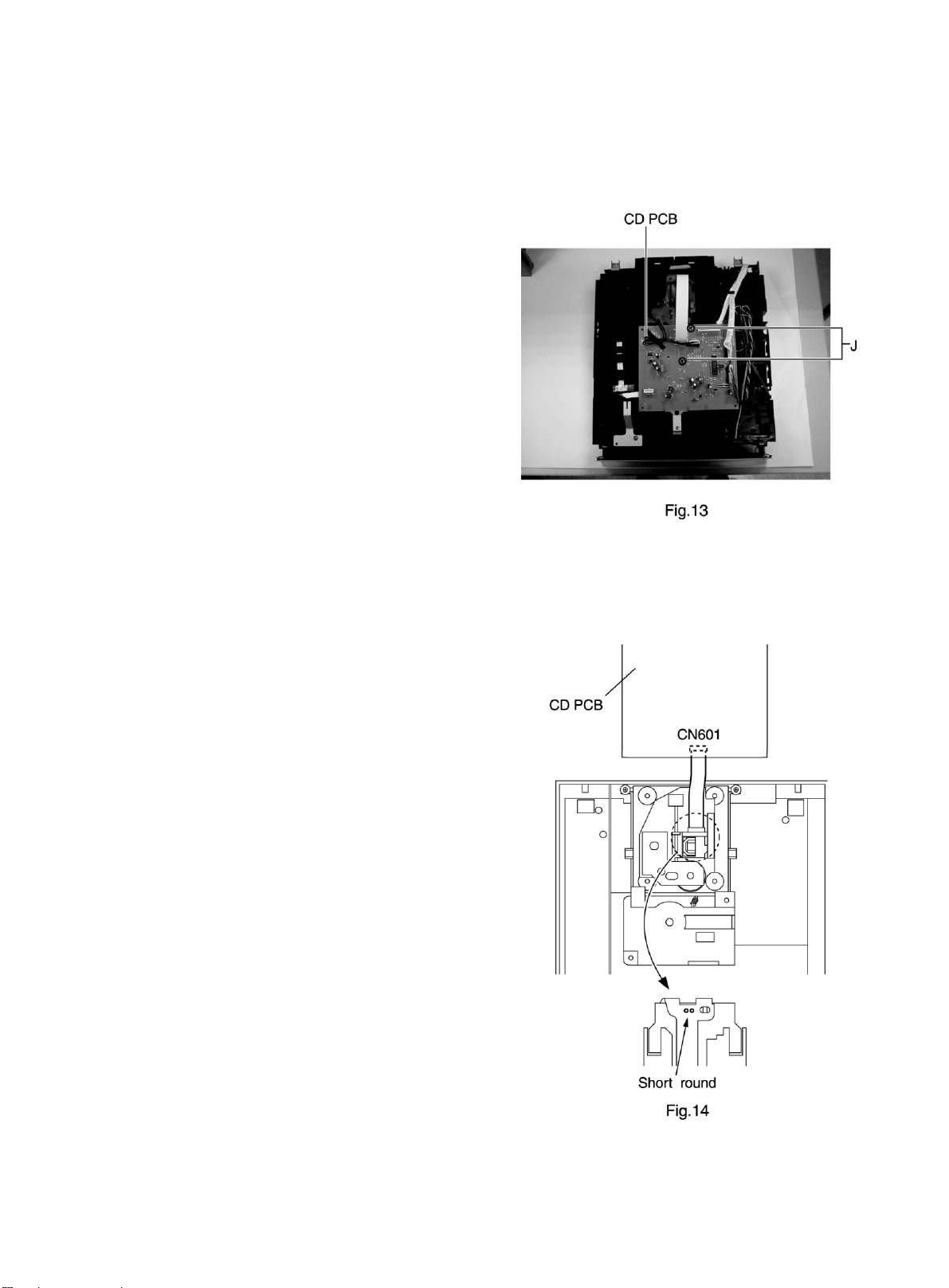
3. Solder is put up before the card wire is removed from connector
Cn601on the main board a s shown in Fig.1 a nd Fig. 2.
(When the wire is removed without putting up solder, the CD
pick-up assembly might destroy.)
4. Please remove solder after connecting the card wire with
CN601 when you install picking up in the substrate.
1-4
Page 5

Disassembly method
Commence disassembly of this set by removing the main units and then proceed to the components and
assemblies inside the units.
Replacement of the fuses and the power IC
n Top cover
n CD changer unit
n Front panel assembly
n Chassis unit
n CD changer unit
n Removing the main PCB
n Removing the CD changer mechanism assembly
n Removing the CD pickup
n Replacing the loading motor and belt of the CD changer tray
n Replacing the CD tray rotor belt of CD changer, and removing the motor
n Front panel assembly
n Removing the cassette deck mechanism
n Removing the earphone jack PCB
n Removing the control/FL PCB
n Removing the switch PCB and ACTIVE BASS EX. switch PCB
n Removing the cassette deck main motor, and replacing the main belts
n Removing the leaf switches of the cassette deck me chanism
n Removing the cassette deck heads
n Chassis unit
n Removing the 3-pin regulator
n Removing the power amp and supply PCB and the Power Trans PCB
n Removing the sub power PCB
1-5
Page 6
<Disasse mbly of the main blocks of this set>
Repla c ement of the fuses and the power IC
n Re pla cing the fuse s (See Fig.1, Fig.4)
n
Prior to performing the following procedure, remove
the left side BOARD a nd remove tuner PCB (Fig.4,BB)
1. Replace the fuses in side.
[Caution] Be sure to use fuses with the specified ratings.
For CA-MXK10R/15R Fig.1(A)
BOTTOM SIDE
CN981
CAUTION
(don’t remove
the safety sheet
cover )
For CA-MXK10R/15R Fig.1(A)
Component SIDE
Fuse(F981)
T1AL 250V
Fuse(F952)
T1.6AL 250V
FW981
Fuse (F981)
T2AL 250V
CN981
For CA-MXK30R Fig.1(B)
BOTTOM SIDE
HOLE
Fuse Hole
For CA-MXK30R Fig.1(B)
Component SIDE
CAUTION
(don’t remove
the safety sheet
cover )
Fuse(F952)
FW951
Fuse (F952)
T1.6AL 250V
FW981
Fuse(F981)
T1AL 250V
CN981
n Repla cing the power IC (See Fig.2 to 3)
n
Prior to performing the following procedure, remove
the top cover.
1. Remove the two screws "A" from the heat sinkbetween
the power IC.
2. Remove the solder fixing the power IC.
For CA-MXK10R/15R Fig.2
W
A
Fuse(F952)
T1.6AL 250V
For CA-MXK30R Fig.3
Fuse (F981)
T2AL 250V
w
CN981
A
1-6
Page 7
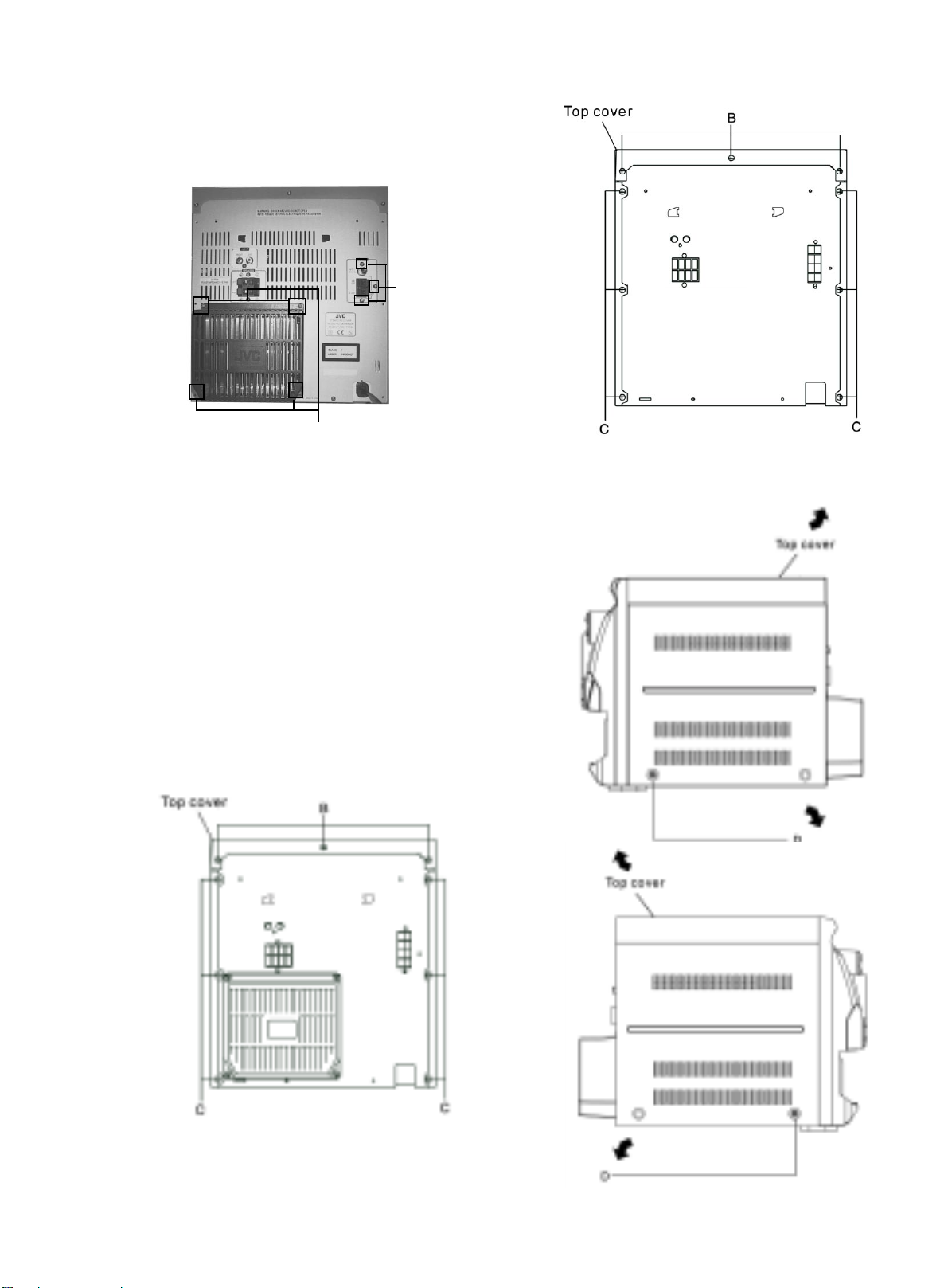
n Repla cing the he at sink cover
1. Remove the six screws "B" from the back pa nel.
2. Pull the heat sink cover outward.
For CA-MXK30R Fig.4
BB
B
n Re moving the top cover a nd two side s BOAR D
(See Fig.5 and 6)
1. Remove the six screws "C" that retain the top cover from the
rear of the body.
For CA-MXK15R Fig.5(B)
For CA-MXK10R/K30R Fig.6(A)
2. Remove the eight screws "C" and "D" that retain the top from
the two sides of the body.
3. Remove the top cover from the body by lifting it toward the
rear.
For CA-MXK10R/K30R Fig.5(A)
1-7
Page 8
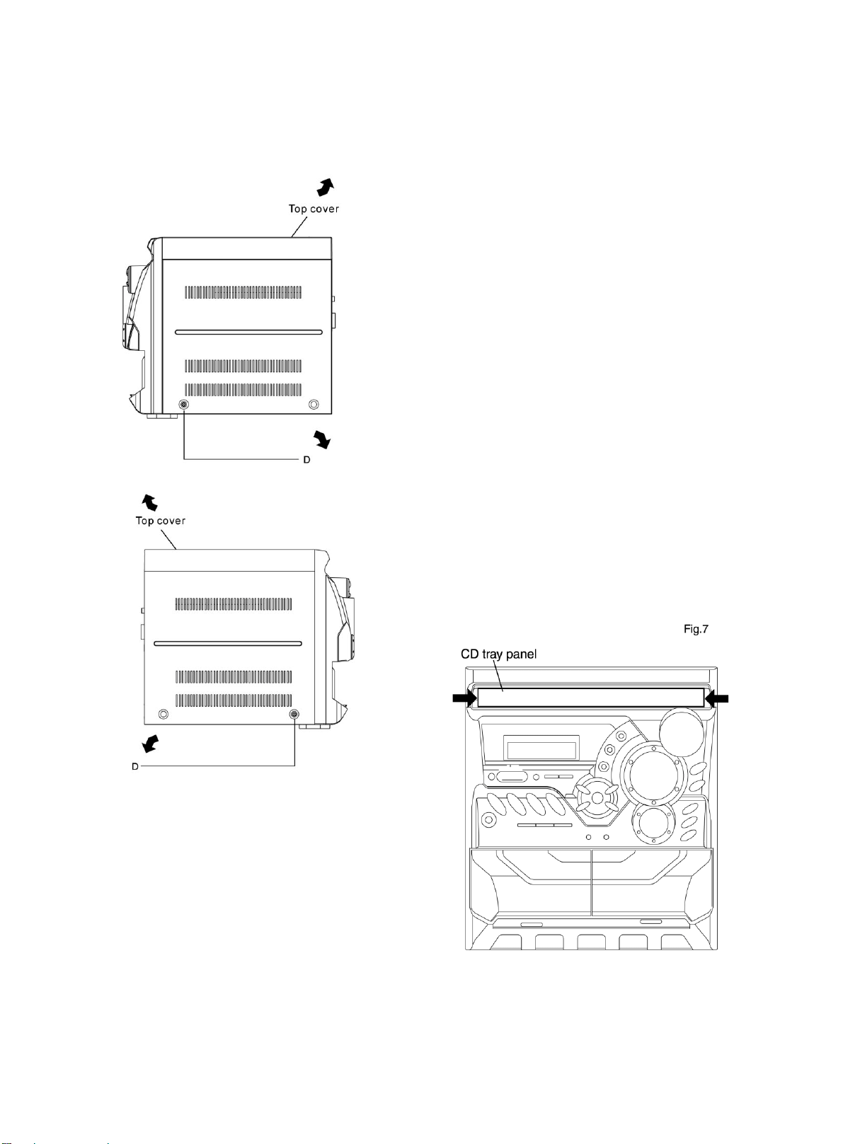
For CA-MXK15R Fig.6(B)
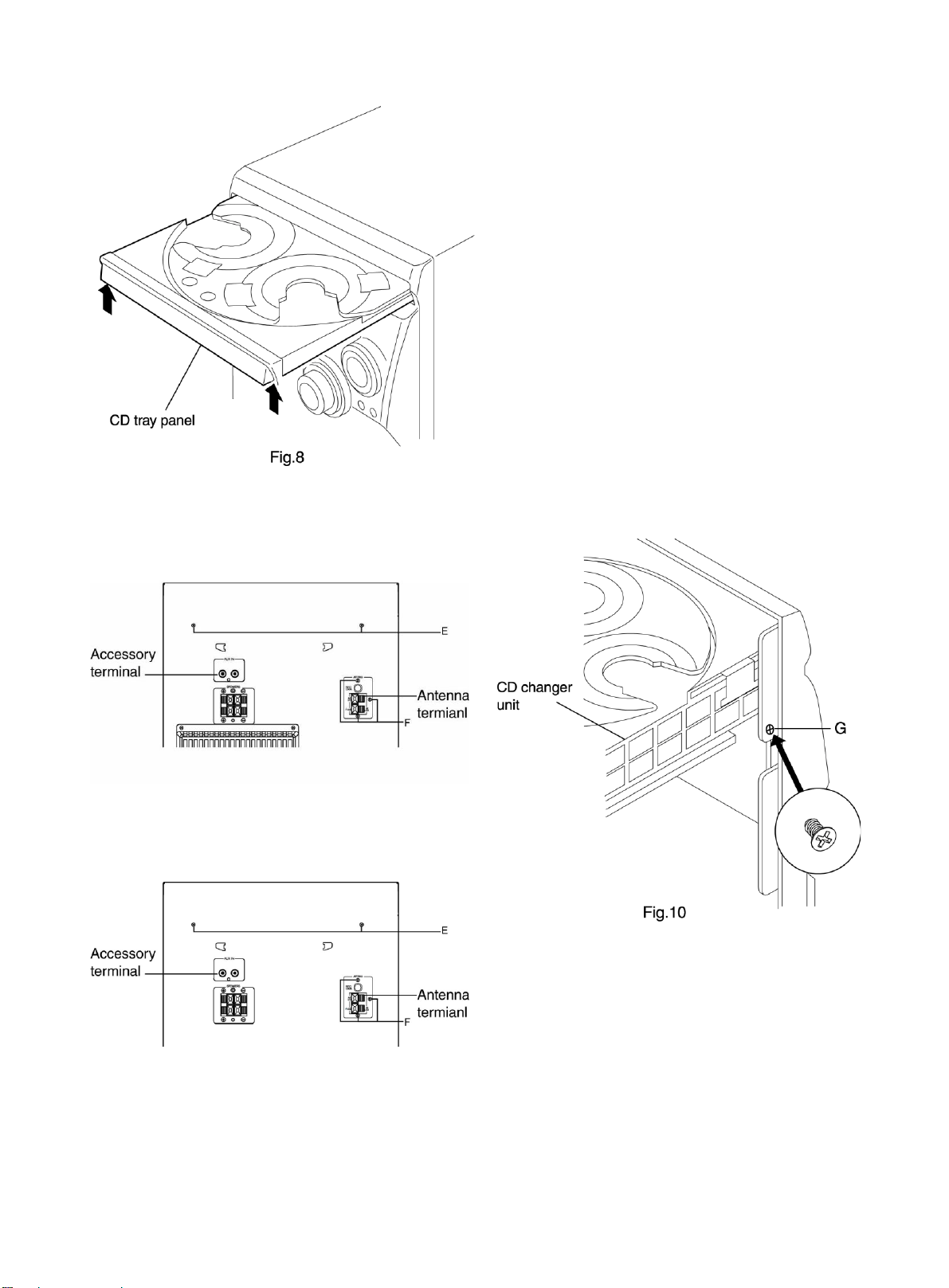
n Removing the CD changer unit
(See Fig.7 to 10)
n
Prior to performing the following procedures, remove
the top cover and both sides BOARD.
[Caution] Although the CD mechanism unit can be
removed without removing the CD tray
panel, it is still recommended to remove it
in order to prevent da mage.
a. From the front panel side of this set, push in the sec-
tions marked with arrows and pull out the CD tray
toward the front.
b. Remove the CD tray panel by pushing both of its ex-
tremities upward in the direction of the arrows.
c. Push the CD tray deep into the set.
1. Disconnect the card wires from the CD PCB CN703
and CN203.
2. From the rear of the set, remove the two screws "E"
and two serews "G" on the front panel left and right
side.
3. Handle the CD changer unit rear, ta ke out unit.
1-8
Page 9
For CA-MXK10R/30R Fig.9(A)
For CA-MXK15R Fig.9(B)
1-9
Page 10
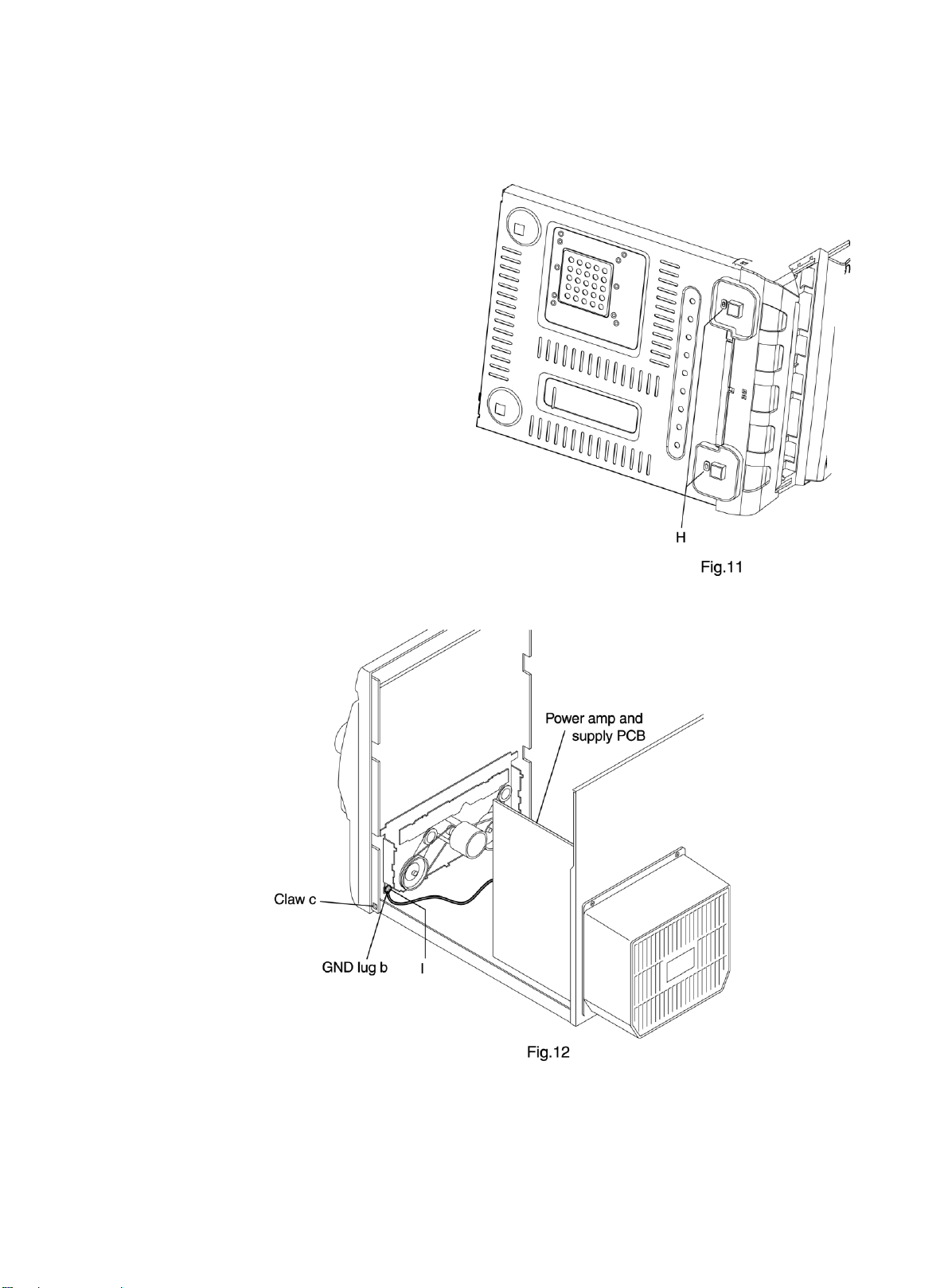
n Removing the front panel assembly
(See Fig.11 and 12)
n
Prior to performing the following procedures, remove
the top cover and both sides board.
n
Also remove the CD cha nger unit.
1. Disconnect the parallel wire and card wire from the
connectors CN702,CN701,CN101on the power a mp
and supply PCB.
2. Remove the two screws "H" retaining the front panel
assembly onto the bottom of the body.
3. Remove the screw "I" retaining the cassette deck
mechanism and then remove then GND lug "b" that
comes from the power a mp and supply PCB.
4. Disengage the claws "c" on both side s at the bottom
of the front panel assembly and then remove the
assembly.
1-10
Page 11
<Disa ssembly of units a nd a sse mbly inside
this set>
n Removing the CD PCB
(See Fig.13 and 14)
n
Prior to performing the following procedures, remove
the top cover and both sides board.
n
Also remove the CD cha nger unit.
1. Disconnect the wires from CN603A, CN603B and
CN604 on the CD PCB, which is located on the back
side of the CD changer unit.
2. The two screws "J" that retain the CD PCB should
be removed.
3. Remove the CD PCB by pulling it toward the side
where the CN601 is located.
4. Using solder, short the CD pickup to connect to short
round.
[Caution] After re-connecting the wires, be sure to
remove the shorting solder from the GND
connection.
5. Disconnect the card wire from the conne ctor CN601
on the main PCB and then remove the main PCB.
1-11
Page 12
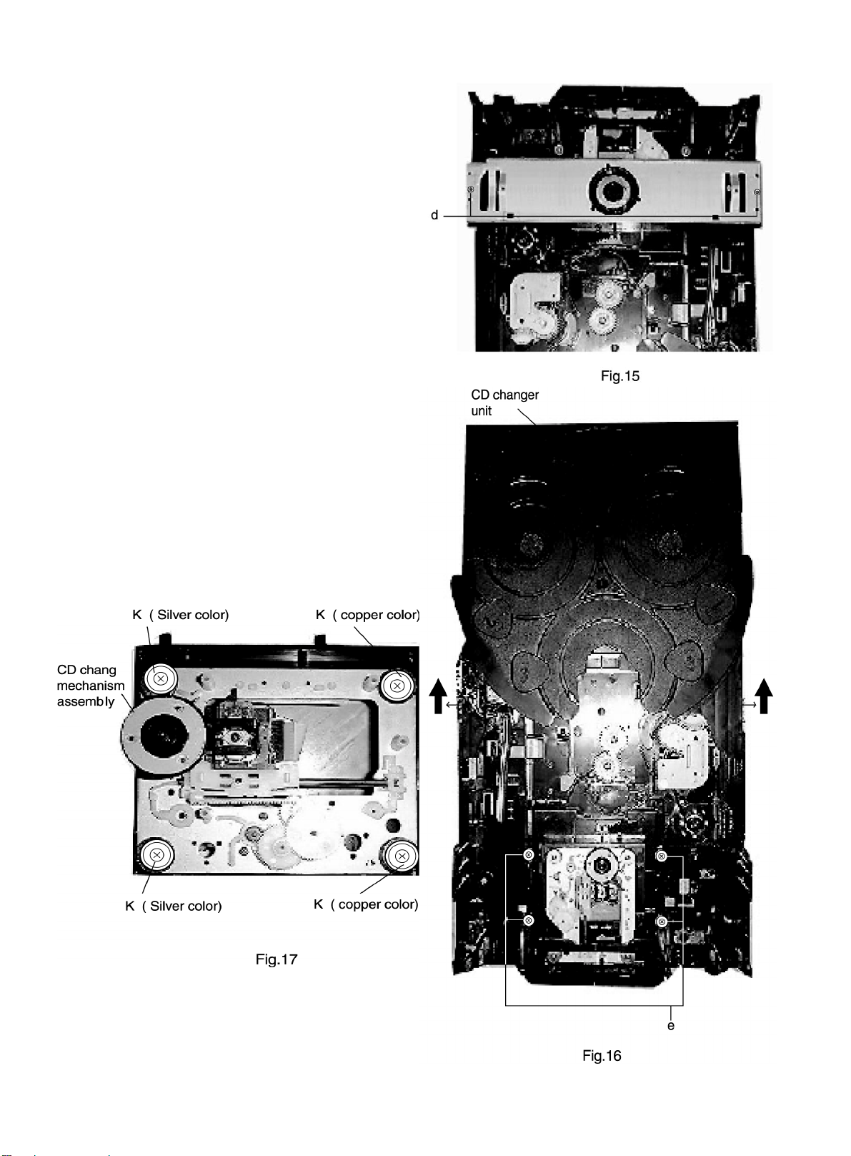
n Removing the CD changer mechanism
assembly
n
Prior to performing the following procedures, remove
the top cover and both sides board.
n
Also remove the CD cha nger unit.
1. Remove the screws "d" from the front chuch ba se of
the CD cha nger me cha nism unit.
2. Turn the CD changer mechanism cover base and
remove the screws "e" connecting the unit to the CD
changer mecha nism assembly.
3. Removing the four screws "k" retaining the CD
mechanism holder assembly.
[Caution] When repla cing the CD cha nger mecha nism
assembly, be sure not to mistake the
positions of the silver color and copper color
spring.
(See Fig.15 to 17)
1-12
Page 13
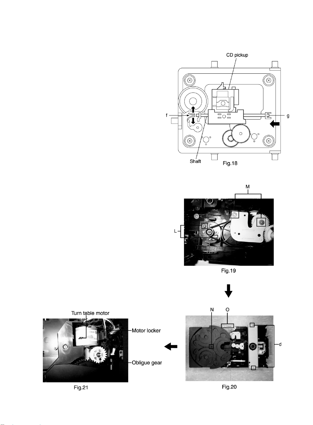
n Removing the CD pickup (See Fig.18)
n
Prior to performing the following procedures, re-
move the top cover and both sides board.
n
Also remove the CD changer unit.
n
Also remove the CD changer mechanism.
1. Widen the section "f".
2. While keeping the section "f" wide open, push
the section "g" in the direction of the arrow to
remove the shaft, and then remove the CD pickup.
n Replacing the loa ding motor and rotor belt
of the CD changer (See Fig .19)
n
Prior to performing the following procedure, re-
move the top cover.
n
Also open the CD changer tray.
1. Remove the two screws "L" retaining the CD
changer tray loading motor.
2. Remove the two screws "M" retaining the gear
plate and take it out, after remove the rotor belt
from the pulley.
n Replacing the CD turn table and remov-
ing the motor (See Fig. 20 and 21)
n
Prior to performing the following procedures, re-
move the top cover.
n
Also remove the CD changer unit.
1. Remove the one screws "N" retaining the CD (Turn
table).
2. Remove the two screws "O" retaining the stopper brackets on both sides of the CD cha nger unit.
3. Remove the stopper brackets from both sides of
the CD changer unit.
4. Pull out the CD tray from the CD changer unit, all
the way and lift the tray (u/~ ward) to remove.
5. Remove the gear and after push out the tray motor
locker and pull out the tray motor from the CD
tray.
1-13
Page 14
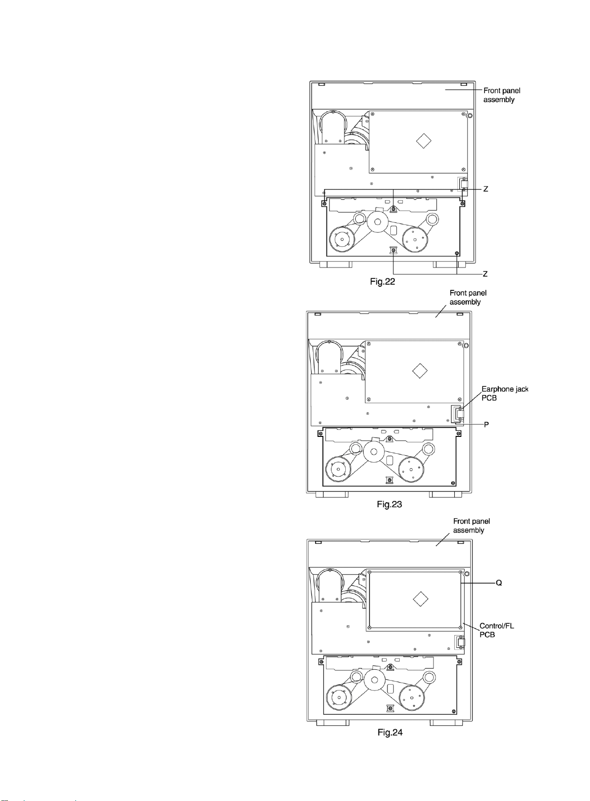
n Removing the cassette deck mechanism
(See Fig.22)
n
Prior to performing the following procedure, remove
the top cover and both sides board.
n
Also remove the CD cha nger unit.
n
Also remove the front panel assembly.
1. Remove the five screws "Z" retaining the ca ssette deck
mechanism.
n Removing the earphone jack PCB
(See Fig.23)
n
Prior to performing the following procedure, remove
the top cover and both sides board.
n
Also remove the CD cha nger unit.
n
Also remove the front panel assembly.
1. Remove the screw with the washer, "P" that retains
the earphone jack PCB.
nRemoving the control/FL PCB
(See Fig.24)
n
Prior to performing the following procedure, remove
the top cover and both sides board. Also remove the
CD cha nger unit.
n
Also remove the CD cha nger unit.
n
Also remove the CD cha nger unit.
1. Remove the four screws "Q" that retain the control/FL
PCB from the back of the front pa nel unit.
1-14
Page 15
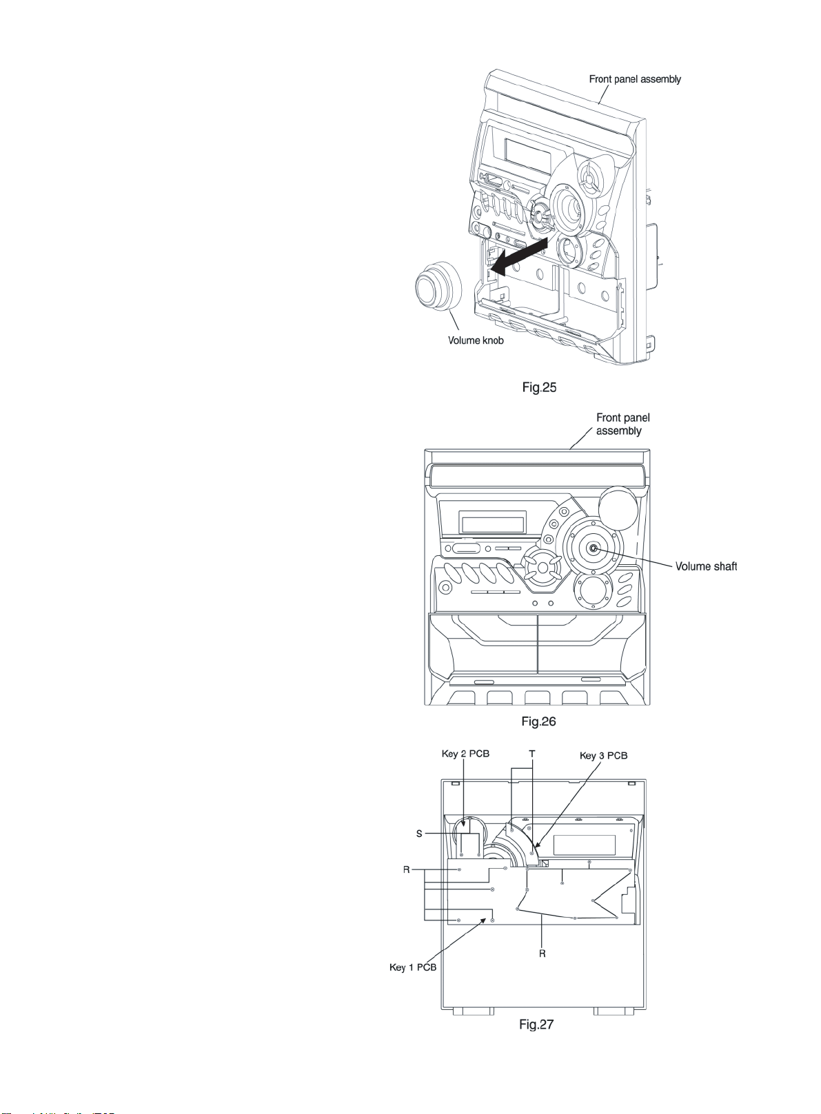
Removing the switch PCB and sound
mode and CD function switch PCB
(See Fig.24 to 27)
Prior to performing the following procedures, remove
the top cover and both sides board.
Also remove the CD changer unit.
Also remove the front panel assembly.
1. Pull out the volume control knob from the front of the
front panel assembly.
2. Remove the four screws "Q" retaining the front panel
assembly.
3. Remove the control / FL PCB.
4. Remove the eleven screws "R" retaining the switch
(key 1) PCB.
5. Remove the three screws "S" retaining the sound mode
(key 2) switch PCB.
6. Remove two screws "T" retaining the CD function (key
3) switch PCB.
1-15
Page 16
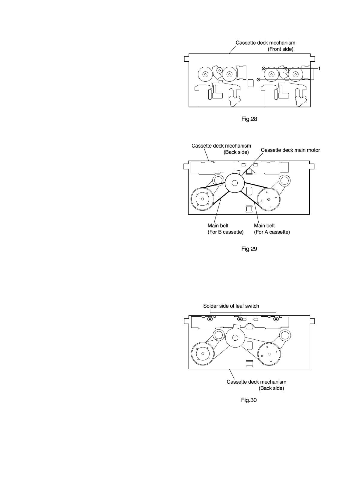
n Re moving the ca ssette de ck main motor ,
and re placing the main belts
(See Fig. 22, 28 and 29)
n
Prior to performing the following procedures, remove
the top cover and both sides board.
n
Also remove the CD cha nger unit.
n
Also remove the front panel assembly.
1. Remove the five screws "z" retaining the ca ssette deck
mechanism.
2. Remove the ca ssette deck me chanism.
3. Remove the two screws "t" retaining the main motor
from the front side of the ca ssette deck.
[Caution] After attaching the main motor, check the
orientation of the motor and the polarity of
the wires.
4. From the backside of the cassette deck, remove the
main motor and two main belts.
[Caution] The lengths of the cassette A (playback
only) and cassette B (record/play) main
belts are different. When atta ching the main
belts, use the longer belt for cassette A.
n Removing the leaf switches of the cas-
sette deck mechanism
(See Fig. 22 and 30)
n
Prior to performing the following procedures, remove
the top cover and both sides board.
n
Also remove the CD cha nger unit.
n
Also remove the front panel assembly.
1. Remove the five screws "O" that retain the cassette
deck mechanism.
2. Remove the ca ssette deck me chanism.
3. Turn the cassette deck mechanism upside down.
4. Remove the solder from around the leaf switches.
5. Pull out the leaf switches from the front side of the
cassette deck mechanism.
1-16
Page 17
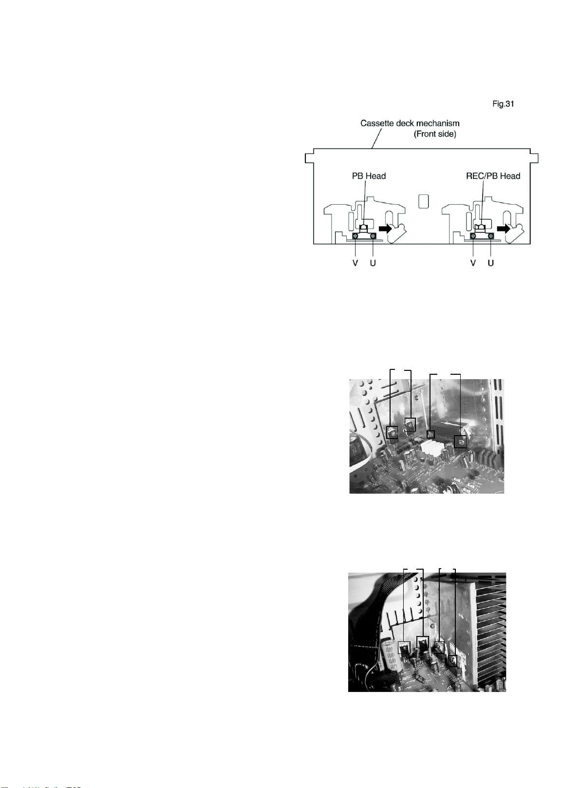
n Removing the cassette deck heads
(See Fig. 22 and 31)
n
Prior to performing the following procedures, remove
the top cover and both side board.
n
Also remove the CD cha nger unit.
n
Also remove the front panel assembly.
1. Remove the five screws "O" that retain the cassette
deck mechanism.
2. Remove the ca ssette deck mecha nism a nd pla ce it so
that the front side faces up.
3. Remove the solder from the bottom side of the head
terminal and disconnect the wire.
4. Remove the screw "U" that retains the head.
5. Remove the screw "V" that retains the head.
6. Hold the head and slide it in the direction of the arrow
to remove it.
n Removing the 3-pin regulator
(See Q904, Q907, 32 and 33)
n
Prior to performing the following procedures, remove
the top cover and both sides board.
1. Remove the two screws "A" that connect the heat
sink cover to the rear panel.
2. Pull the heat sink outward.
3. Remove the screw "W" that retains the heat sink the
3-pin terminal regulator Q904,Q907.
4. Remove the solder fixing the 3-pin regulator.
For CA-MX K30R Fig.32
w
For CA-MX K10R/K15R Fig. 33
W
A
A
1-17
Page 18
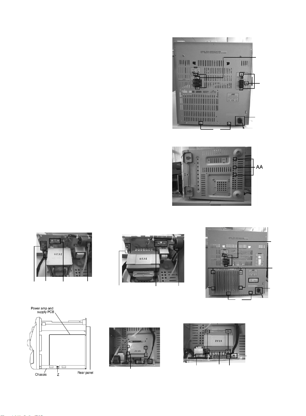
n Removing the power amp and supply
PCB and the power trans PCB
(See Fig. 2, 3, 32, 34 to 37)
For CA-MXK10R/K15R Fig.34(A)
n
Prior to performing the following procedures, remove
the top cover and both sides board.
n
Also remove heat sink cover .(Fig.4)
1. Remove the two screws "A" connecting the heat sink
cover to the rear panel.(Fig.2, 3)
2. Pull out the heat sink cover toward you.
3. Remove the three (CA-M XK10/K15R)/ four(CA-MXK30)
screws "AA" form the (CA-MXK10/K15R) chassis /
MX-K30 back panel between the heat sink.
4. Remove the three screws "X" that retain the speaker
terminals and AUX terminal.
5. Remove the screw "YY" that retains the rear panel,
and then remove the re ar panel.
6. Disconnect the parallel wires from the connectors
FW951 and CN981 on the power tra n s PCB.
7. Remove the screw "Z" that retain the power a mp a nd
supply PCB and then remove the assembly.
8. Remove the cla mp of AC power cord from the cha ssis.
9. Remove the four screws "AB" that retain the power
trans PCB and then remove the assembly.
X
BB
CLAMP
YY
For CA-MXK10R/K15R Fig.34(A)
For CA-MXK10R/K15R Fig.35 (A)
Component SIDE
Fuse (F952)
T1.6AL 250V
FW981
Fuse(F981)
T1AL 250V
Fig.36
CN981
For CA-MXK30R Fig.35(B)
Component SIDE
Fuse(F952)
T1.6AL 250V
For CA-MXK10R/K15R Fig.37 (A)
AB
Fuse (F981)
T2AL 250V
For CA-MXK30R Fig.34(B)
CN981
For CA-MXK30R Fig.37(B)
Fuse F981
T2AL 250V
AB
X
Y
CLAMP
YY
Fuse F952
T1.6AL 250V
FW 951
1-18
Page 19

Adjustment method
Measurement instruments required
for adjustment
1. Low frequency oscillator,
This oscillator should have a capacity to output 0dB
to 600ohm at an oscillation frequency of 50Hz20kHz.
2. Attenuator impedance : 600ohm
3. Electronic voltmeter
4. Frequency counter
5. Wow flutter meter
6. Test tape
VT712 : For Tape speed and wow flutter ( 3kHz)
VT703 : For Head a ngle(10kHz),Play ba ck frequency
characteristics(1kHz), and dubbing
frequency characteristics (63,1,10kHz)
7. Blank tape
TAPE I : AC-225
8. Torque gauge : For play and back tension forward ;
TW2111A, Reverse ; TW2121A Fast Forward and
Rewind ; TW2231A
9. Test disc: CTS-1000(12cm),GRG-1211(8cm)
10. Jitter meter
Measurement conditions
Power supply voltage
AC230V (50Hz)
Measurement
output terminal : Speaker out
: TP101(Measuring for TUNER/
DECK/CD)
: Dummy load 6ohm
Radio input signal
AM modulation frequency : 400Hz
Modulation factor : 30%
FM modulation frequency : 1kHz
Frequency displacement : 22.5kHz
Frequency Range
FM 87.5MHz~108MHz
MW 522kHz~1629kHz
LW 144kHz~228kHz
Standard me asurement positions of
volume and switch
Power: Standby (Light STANDBY Indicator)
S, A, BASS : OFF
Sound mode : OFF
Main VOL. : 0 Minimum
Travers mecha set position : Disc 1
Precautions for measurement
1. Apply 30pF and 33kohm to the IF sweeper output
side and 0.082
sweeper input side.
2. The IF sweeper output level should be made as low as
possible within the adjustable range.
3. Since the IF sweeper is a fixed device, there is no
need to adjust this sweeper.
4. Since a ceramic oscillator is used, there is no need to
perform any MPX adjustment.
5. Since a fixed coil is used, there is no need to adjust
the FM tracking.
6.The input and output earth systems are separated. In
case of simultaneously measuring the voltage in both
of the input and output syst ems with an electronic
voltmeter for two cha nnels, theref ore, the e arth should
be connected particularly.
7. In the case of BTL connection amplifier, the minus
terminal of speaker is not for earthing. Therefore, be
sure not to connect any other earth terminal to this
terminal. This system is of an OTL system.
F and 100kohm in series to the
1-19
Page 20
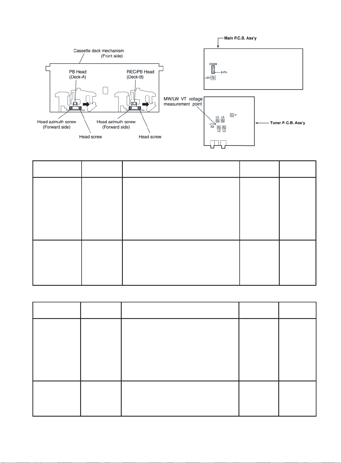
Arrangement of adjusting positions
Tape recorder section
Items
Cassette Head
Azimuth Alignments
Recordi ng Bi as
Frequency Alignment
Tuner section
Items
AM Tracking
Alignments
Measurement
condi tions
Test tape :
VT703 (10kHz)
Measurement
output terminal :
Left and Right
speaker output
(6-ohm loaded)
or Headphone
Output
(32-ohm loaded)
Test tape :
TYPE I AC-225
Measurement
output terminal :
Erase head
terminal
(CN308 8-Pin)
Measurement
condi tions
Input signal :
529kHz (530kHz)
603kHz (600kHz)
Measurement
point :
Resistor(R3)
terminal
Measu rement meth o d
1. Playback the test tape VT703 (10KHz) or equivalent.
2. Adjust the head azimuth screw to obtain maximum
output and both output of L / R is in 3dB.
3. Put on the screw lock paint after alignments.
1. Insert the recording tape in deck-B.
2. Starting the recording.
3. Adjust the oscillation frequency to 80KHz+/-3KHz
by core of Oscillation coil of L301.
Measurement method
1. Set the Signal Generator signal to 529KHz (530KHz)
the feed to Loop Antenna.
2. Receiving the signal and the adjust the OSC coil
L4(MW)/L5(LW) obtain the V.T is 1.40V +/-0.05V.
3. Change the receiving frequency to 603KHz (600KHz).
4. Adjust the Antenna coil L2(MW)/L3(LW) obtain
maximum sensiti vity .(Adjust the SSG output to
out of AGC range.)
Standar d
values
Maximum output Head azimuth
80kHz+/-3kHz Bias coil: L301
Standard
values
V.T :
1.40V+/-0.05V
Maximum
sensitivity
Ad ju stin g
posi tions
screw
Adjust the
head azimuth
screw only
when the head
has been
changed.
Use the HighImpedance
Probe or
Frequency
counter input.
Ad ju stin g
posi tions
OSC coil:
L4(MW)/L5(LW)
Antenna coil:
L2(MW)/L3(LW)
Adjust the OSC
coil only when
the AM coil
block has been
changed.
AM IFT Alignments Input signal :
530kHz (529kHz)
1. Set the receiving frequency to 529KHz (530KHz ).
2. Feed the 450KHz signal to AM antenna input.
3. Adjust the IFT Block T1 obtain to maximum output.
(Adjust the SSG output to out of AGC range.)
Note: The adjustment of CD section is not required.
1-20
Maximum output IFT(T1)
Adjust the IFT
only when the
IFT b lo c k ha s
been changed.
Page 21
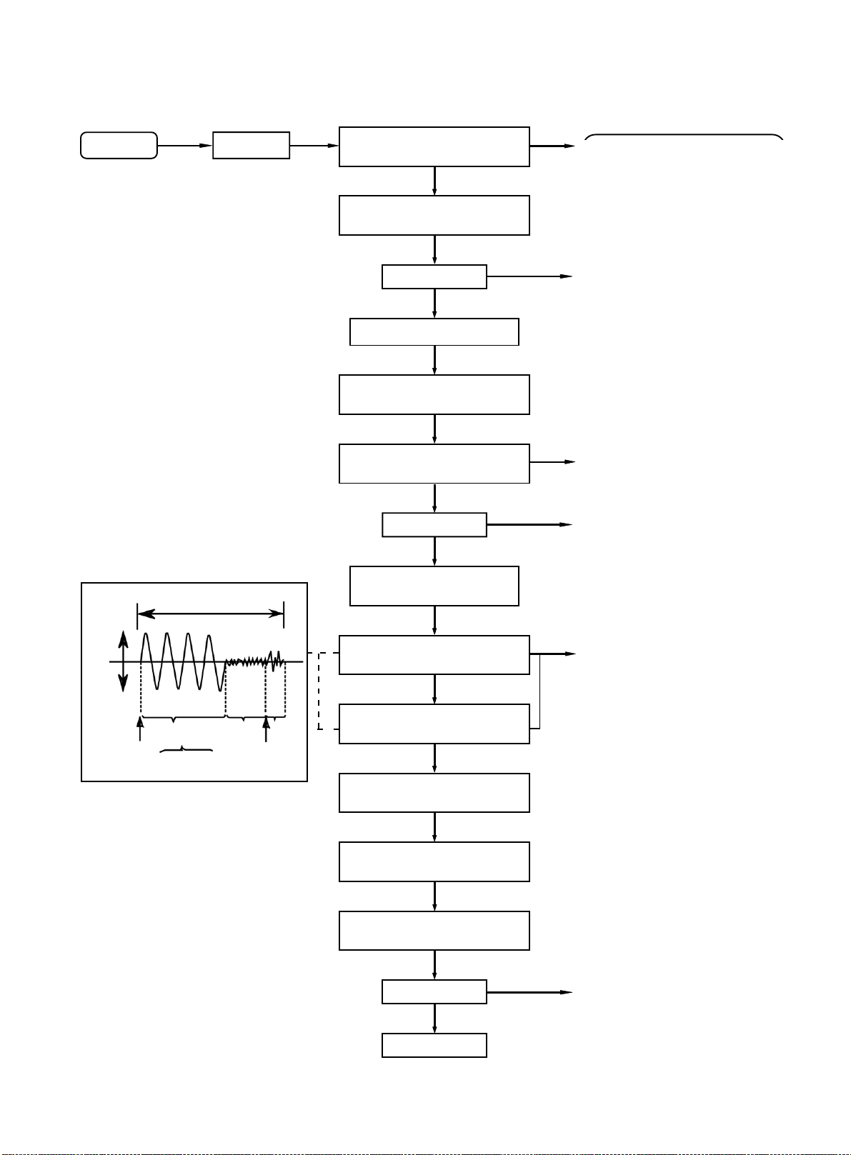
Flow of functional operation until TOC read
Power ON Play Key
Tracking error waveform at TOC reading
n
pin 20 of
IC611(TE)
Approx.3sec
Slider turns REST
SW ON.
Automatic tuning
of TE offset
Laser ON
Detection of disc
Automatic tuning of
Focus offset
Automatic measurement of
Focus S-curve amplitude
Disc is rotated
Focus servo ON
(Tra cking servo ON)
Check Point
Confirm that the voltage at the pin5
of CN602 is "H"\"L"\"H".
Check that the voltage at the pin40
of IC601 is + 5V?
Confirm that the Focus error S-cuve
signal at the pin32 of IC601 is
approx.2Vp-p
Confirm that the signal from pin24
IC601 is 0V as a accelerated pulse
during approx.400ms.
Approx
1.8V
VREF
Disc states
to rotate
Automatic measurement
of TE amplitude and
automatic tuning of
TE balance
Tracking
servo
off states
Tracking
servo
on states
Disc to be
braked to
stop
TOC reading
finishes
500mv/div
2ms/div Fig.1
Automatic measurement of
Tracking error amplitude
Automatic tuning of
Tracking error balance
Automatic tuning of
Focus error balance
Automatic tuning of
Focus error gain
Automatic tuning of
Tracking error gain
TOC reading
Play a disc
Confirm the waveform of the Tracking error signal. at the pin 20 of IC61 1
(R643) (See fig-1)
Confirm the eys-pattern at the lead
of Tp3
1-21
Page 22
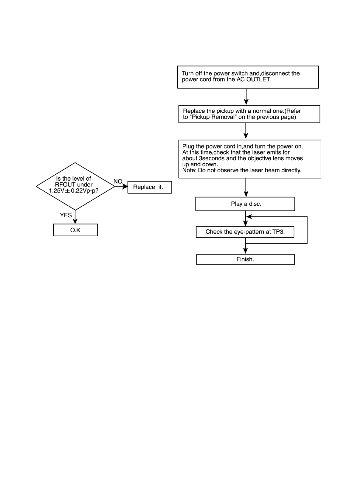
Maintenance of laser pickup
(1) Cleaning the pick up lens
Before you replace the pick up, please try
to clean the len s with a alcohol soaked cotton swab.
(2) Life of the la ser diode
When the life of the la ser diode has expired,
the following symptoms will a ppe ar.
1. The level of RF output (EFM output: a mpli
tude of eye pattern) will below.
Repla cement of laser pickup
(3) Semi-fixed resistor on the APC PC board
The semi-fixed resistor on the APC printed circuit board which is attached to the pickup is used to adjust the
laser power. Since this adjustment should be performed to match the chara cteristics of the whole optical block,
do not touch the semi-fixed resistor.
If the la ser power is lower than the specif ied value, the la ser diode is almost worn out, and the laser pickup should
be replaced.
If the semi-fixed resistor would be adjusted when the pickup operates normally, the laser pickup may be damaged due to excessive current.
1-22
Page 23
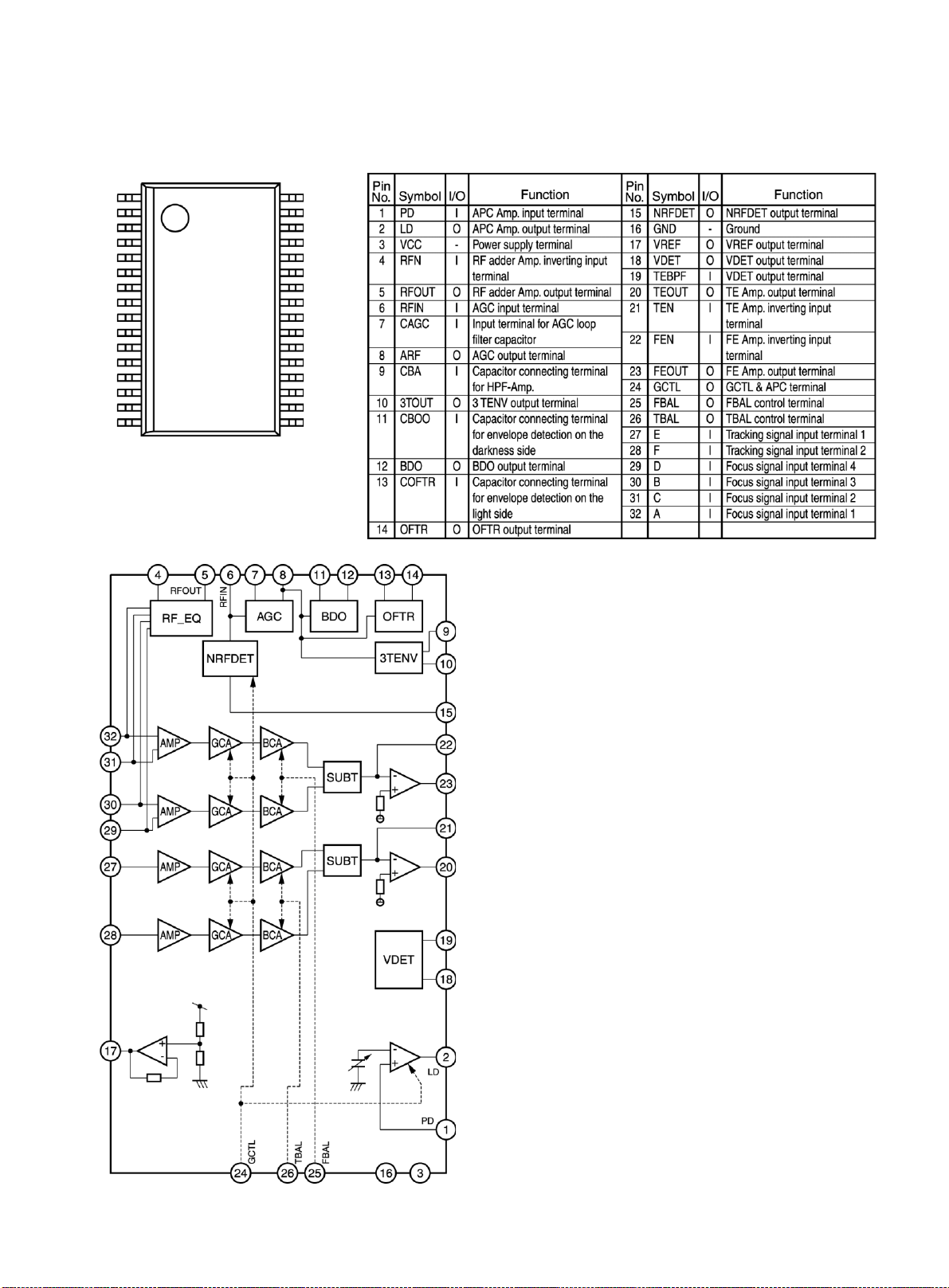
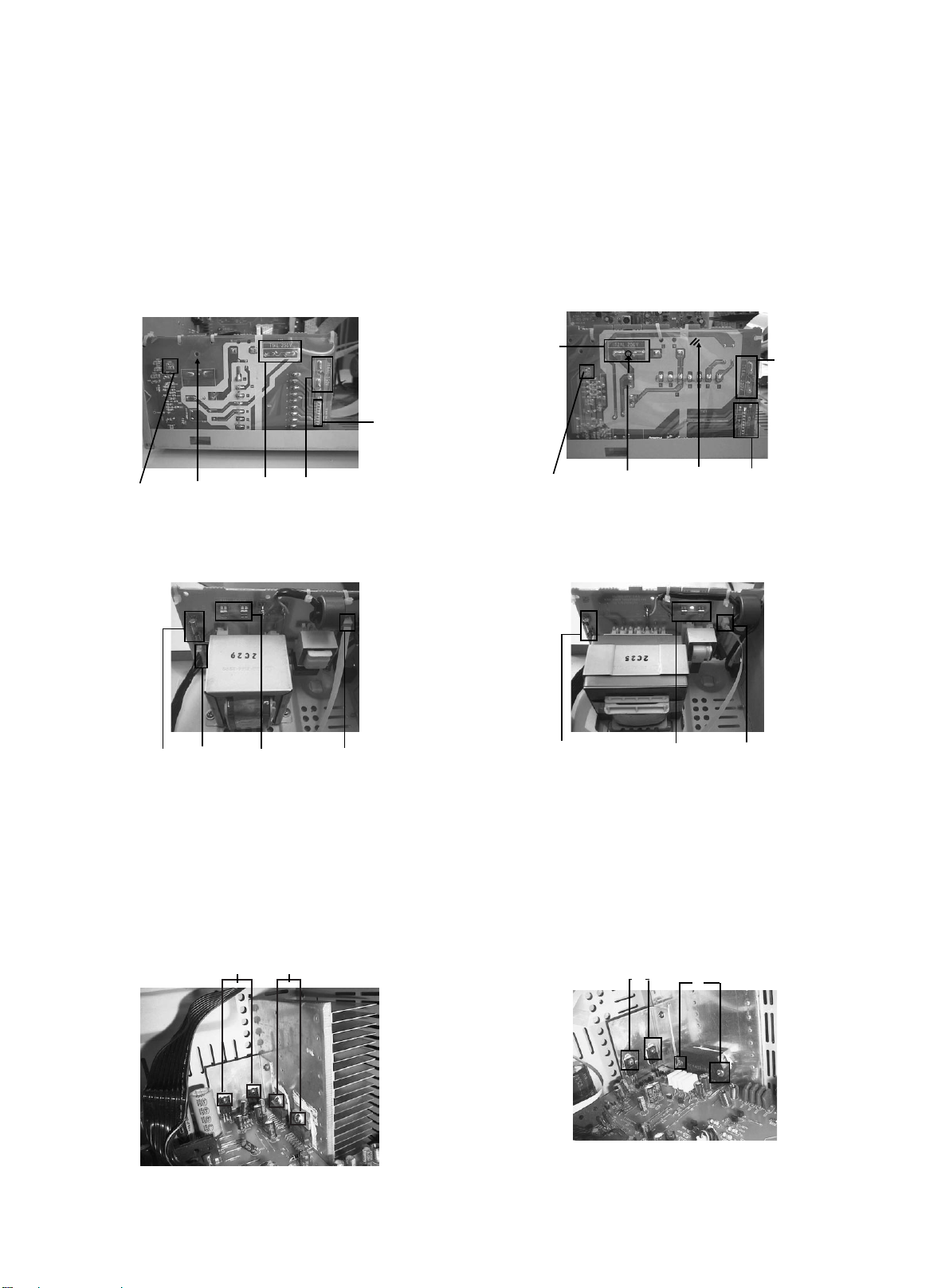
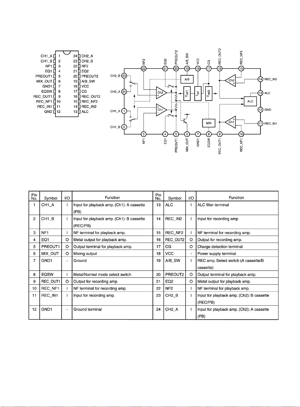
Description of major ICs
n AN22000A (IC611) : CD-DA Head Amp.
1. Terminal layout 2. Pin function
1 3 2
16 17
3. Block diagram
1-23
Page 24
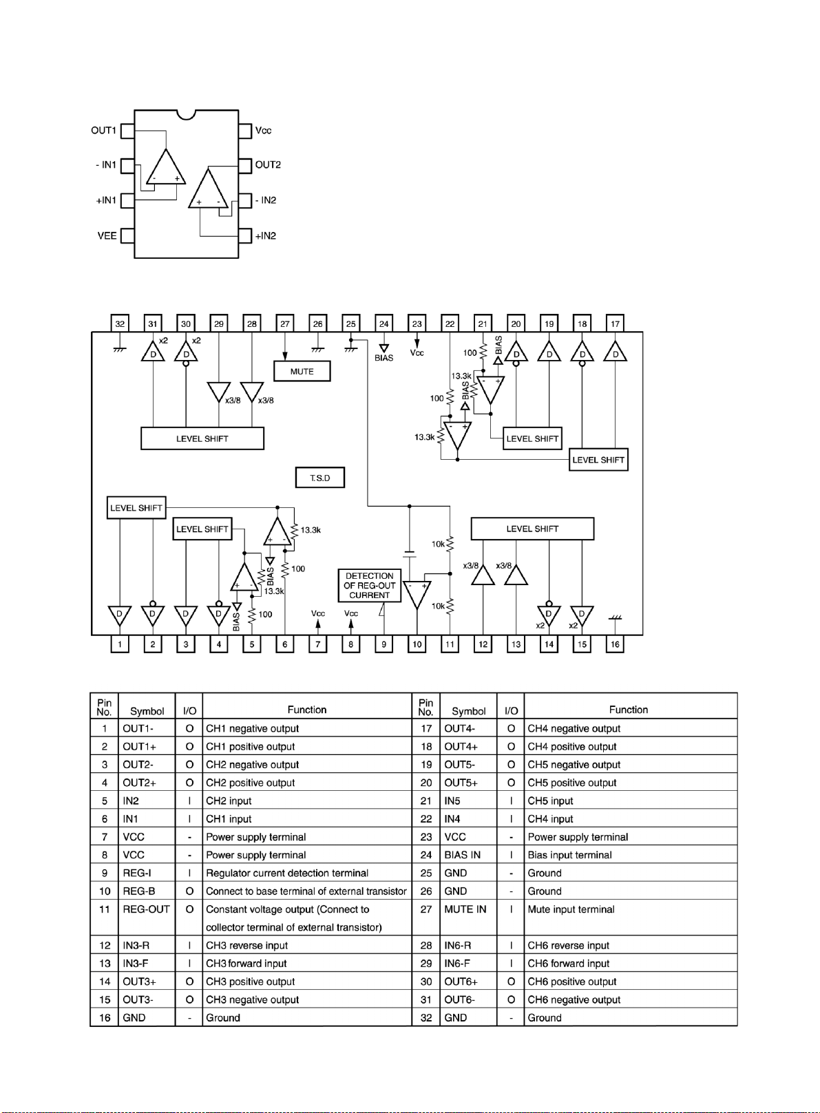
n BA15218DIP (IC102) : Dual low noise operational amp.
1. Terminal layout
n BA5936S (IC621) : 6 channel BTL driver
1. Block diagram
2. Pin function
1-24
Page 25
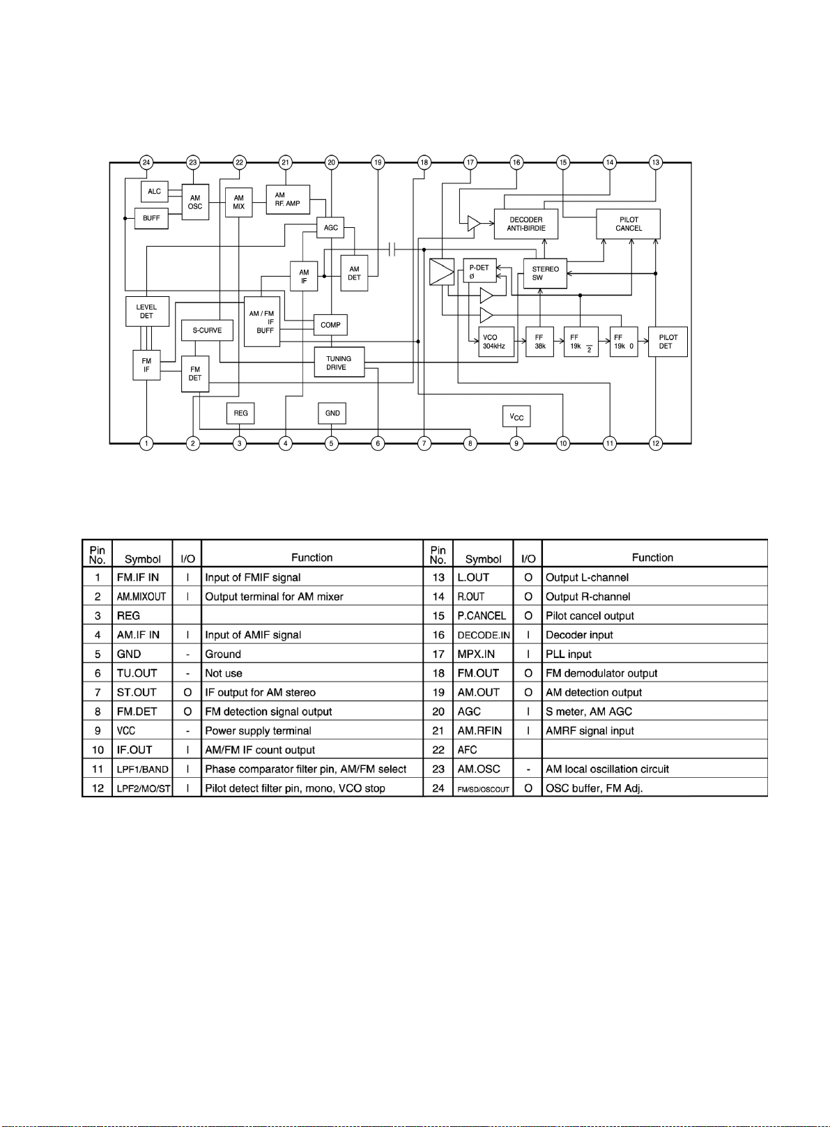
n LA1833 (IC1) : 1chip AM/FM, MPX tuner system
1. Block diagram
2. Pin function
1-25
Page 26
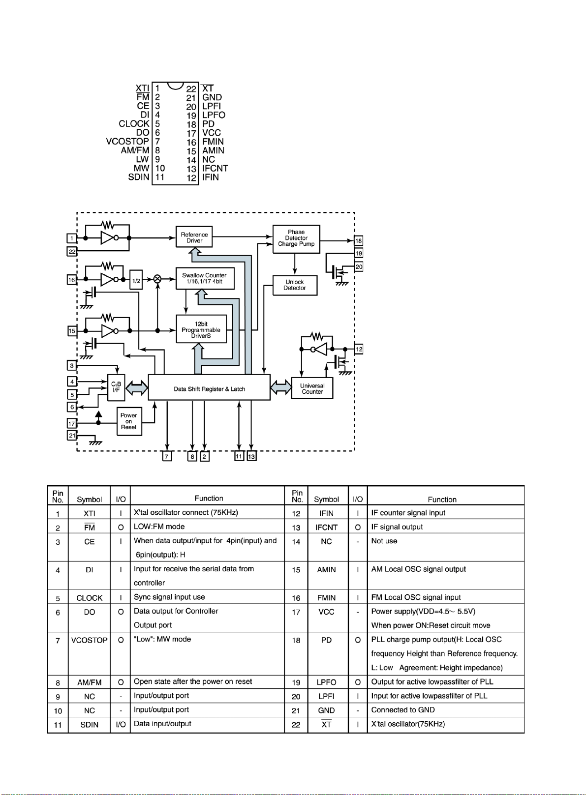
n LC72136N (IC2) : PLL Frequency synthesizer
1.T ermin al layout
2. Block diagram
3. Pin function
1-26
Page 27
n TA8189N (IC401) : REC/PB amp.
1. Terminal layout 2. Block diagram
3. Pin function
1-27
Page 28
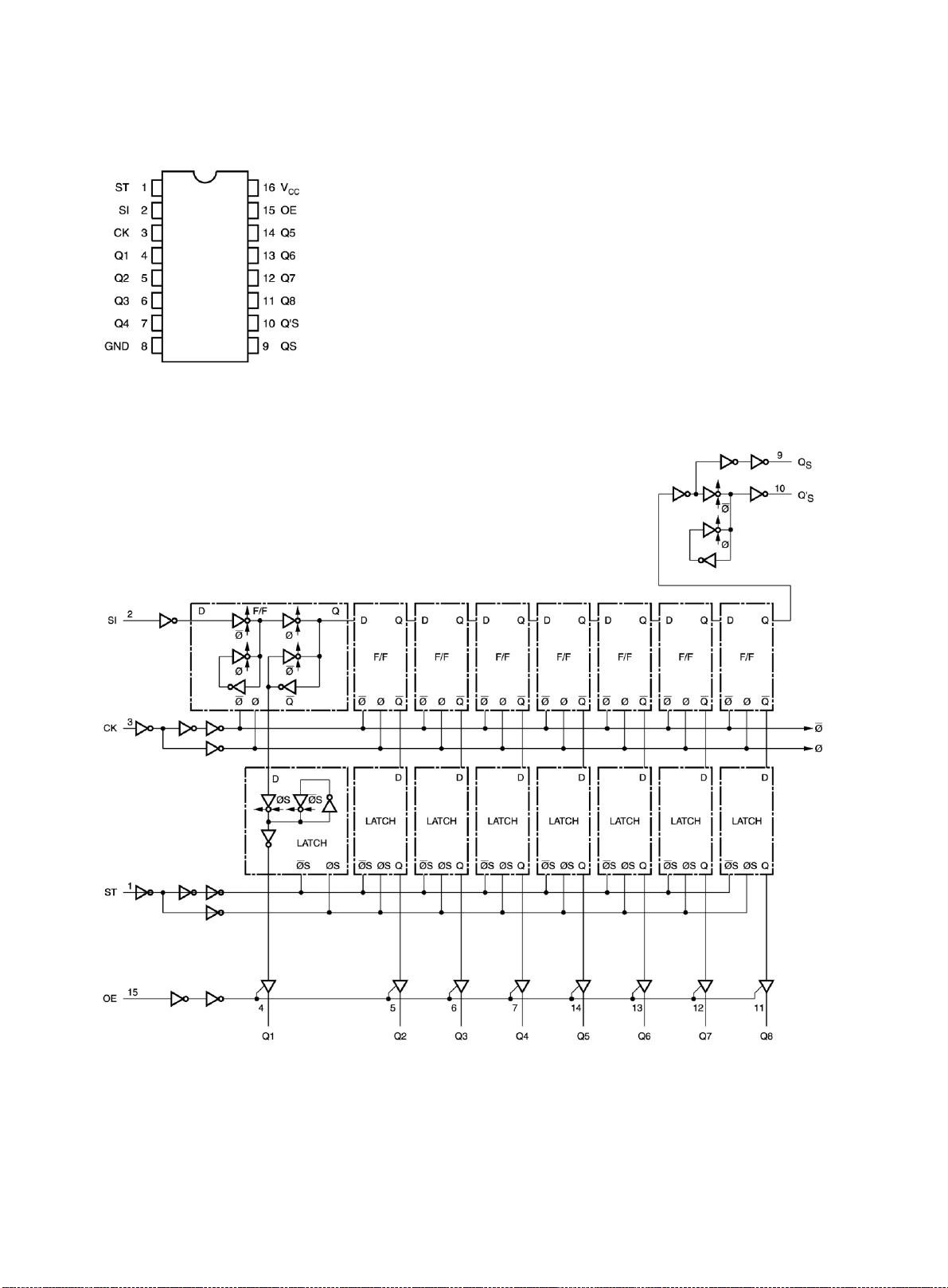
n TC74HC4094AP (IC402) : 8-bit shift and store resister
1.T ermin al layout
2. Block diagram
1-28
Page 29
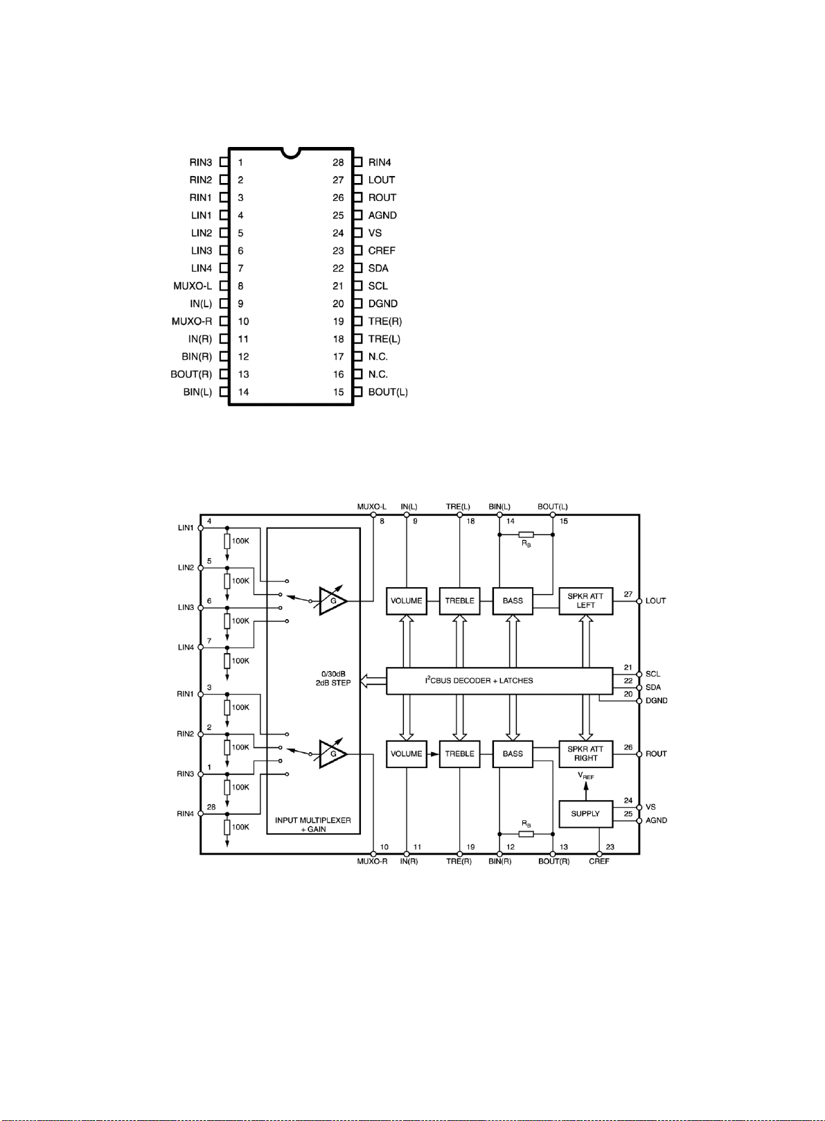
n TDA7440D (IC101) : Audio processor
1. Terminal layout
2. Block diagram
1-29
Page 30
BU1924F (IC3) : RDS/RBDS decoder
1. Terminal layout
2. Block diagram
3. Pin function
1-30
Page 31

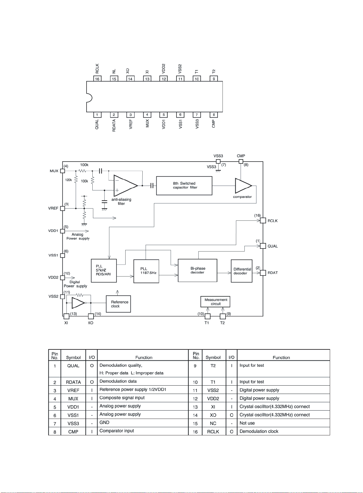
n MN662748RPM (IC601) : Digital servo & digital signal processor
1. Terminal layout
2. Pin function
1-31
Page 32

MX-K10R/K30R/K15R
VICTOR COMPAN Y OF JAPAN, LIMITED
AUDIO & COMMUNICATION BUSINESS DIVISION
PERSONAL & MOBILE NETWORK B.U.10-1, 1 Chome, Ohwatari-machi, maebashi-city, 371-8543, Japan
No.21138
Printed in Japa n
200212
Page 33

MX-K10R/K30R/K15R
SCHEMATIC DIAGRAMS
COMPACT COMPONENT SYSTEM
CD1CD2CD
REPEAT
SOUND
MODE
ACTIVE
BASS EX.
MX-K
10R/K30R/K15R
Area Suffix
MX-K30R
..................
E
.................
EN
..................
B
.................
EV
MX-K10R
..................
E
.................
EN
.................
EV
MX-K15R
.................
EV
Continental Europe
Northern Europe
U.K.
E. Europe/Russia
Continental Europe
Northern Europe
E. Europe/Russia
E. Europe/Russia
REPEAT
SOUND
MODE
ACTIVE
BASS EX.
CD1CD2CD
SELECT
CD-ROM No.SML200212
3-CD
PLAY & EXCHANGE
CD-R/RW PLAYBACK
SOUND
P
COMPACT COMPONENT SYSTEM
STANDBY/ON
SLEEP
AUX
FM MODE
FM /AM
3
CD
PROGRAM
/RANDOM
TAPE
A/B
TAPE
DISPLAY
PTY/EON MODE
FADE
MUTING
VOLUME
MX-K30R
ST
ANDBY/ON
ECO
STANDBY
CANCEL
/ DEMO
CD
TAPE
FM
AUX
/ AM
PHONES
REC START
/ STOPCD REC START DUBBING
SELECT
PTY / EON
DISPLAY MODE
EJECT EJECT
FULL - LOGIC CONTROL
PLAY
A
K
O
C
MODE
REPEAT
P
O
1 BIT
DUAL D/A
R
CONVERTER
PROGRAM
C
L
A
C
I
S
S
E
M
U
L
O
V
PANDOM
SET
CLOCK
/TIMER
PRESET
TUNING
TAPE
A / B
CD SYNCHRO RECORDING
IP
K
S
C
S
I
D
3
CD
ACTIVE
2
D
C
BASS EX.
1
D
C
REC / PLAY
B
SP-MXK30 CA-MXK30R SP-MXK30
BASS-REFLEX BASS-REFLEX
STANDBY/ON
SLEEP
AUX
FM MODE
FM /AM
3
CD
PROGRAM
/RANDOM
TAPE
A/B
TAPE
DISPLAY
SELECT
PTY/EON MODE
FADE
MUTING
VOLUME
3-CD
PLAY & EXCHANGE
COMPACT COMPONENT SYSTEM
MX-K10R
1 BIT
DUAL D/A
CONVERTER
PROGRAM
PANDOM
ST
ANDBY/ON
ECO
STANDBY
SET
CANCEL
/ DEMO
PRESET
CD
TAPE
FM
AUX
/ AM
PHONES
TUNING
REC START
/ STOPCD REC START DUBBING
CLOCK
TAPE
SELECT
PTY / EON
DISPLAY MODE
/TIMER
A / B
EJECT EJECT
CD SYNCHRO RECORDING
FULL - LOGIC CONTROL
PLAY
A
CD-R/RW PLAYBACK
SOUND
P
K
O
C
MODE
REPEAT
P
O
R
C
L
A
C
I
S
S
E
M
U
L
O
V
P
I
K
S
C
IS
D
3
CD
ACTIVE
2
CD
BASS EX.
1
CD
REC / PLAY
B
CD1CD2CD
REPEAT
SOUND
MODE
ACTIVE
BASS EX.
STANDBY/ON
SLEEP
AUX
FM MODE
FM /AM
3
CD
PROGRAM
/RANDOM
TAPE
A/B
TAPE
DISPLAY
SELECT
PTY/EON MODE
FADE
MUTING
VOLUME
BASS-REFLEX BASS-REFLEX
3-CD
PLAY & EXCHANGE
COMPACT COMPONENT SYSTEM
MX-K15R
1 BIT
DUAL D/A
CONVERTER
PROGRAM
PANDOM
ST
ANDBY/ON
ECO
STANDBY
SET
CANCEL
/ DEMO
PRESET
CD
TAPE
FM
AUX
/ AM
PHONES
TUNING
REC START
/ STOPCD REC START DUBBING
CLOCK
TAPE
SELECT
PTY / EON
DISPLAY MODE
/TIMER
A / B
EJECT EJECT
CD SYNCHRO RECORDING
FULL - LOGIC CONTROL
PLAY
A
CD-R/RW PLAYBACK
SOUND
P
K
O
C
MODE
REPEAT
P
O
R
C
L
A
C
I
S
S
E
M
U
L
O
V
P
I
K
S
C
S
I
D
3
D
C
ACTIVE
2
D
C
BASS EX.
1
D
C
REC / PLAY
B
SP-MXK10 CA-MXK10R SP-MXK10 SP-MXK15 CA-MXK15R SP-MXK15
Contents
Wiring Diagram
Standard schematic diagrams
Printed circuit boards
COPYRIGHT 2002 VICTOR COMPANY OF JAPAN, LTD.
2-1
2-2
2-10~
No.21138SCH
Dec. 2002
Page 34

MX-K10R/K30R/K15R
In regard with component parts appearing on the silk-screen printed side (parts side) of
the PWB diagrams, the parts that are printed over with black such as the resistor ( ),
diode ( ) and ICP ( ) or identified by the " " mark nearby are critical for safety.
(This regulation does not correspond to J and C version.)
2-2
Page 35

Standard schematic diagrams K10R/K15R
Head AMP.audio, power AMP. and power supply section
5
4
MX-K10R/K30R/K15R
3
2
1
AB CD E F G
2-1
Page 36

MX-K10R/K30R/K15R
MX-K10R/K30R/K15R
POWER TRANSF ORMER SECTION K10R/15R
5
4
3
2
1
2-2
HAB C DE FG
Page 37

MX-K10R/K30R/K15R
Head AMP. audio, power AMP. and power supply K30R
5
4
3
2
1
AB CD E F G
2-3
Page 38

MX-K10R/K30R/K15R
MX-K10R/K30R/K15R
POWER TRANSFORMER SECTION K30R
5
4
3
2
1
2-4
HAB C DE FG
Page 39

MX-K10R/K30R/K15R
FL display and CPU control section K10R/K30R/15R
5
4
3
2
1
AB CD E F G
2-5
Page 40

MX-K10R/K30R/K15R
MX-K10R/K30R/K15R
CD servo control section K10R/K30R/15R
5
4
3
2
1
2-6
HAB C DE FG
Page 41

MX-K10R/K30R/K15R
TUNER SECTION K10R/K30R/K15R
5
4
3
2
1
AB CD E F G
2-7
Page 42

Printed circuit boards
main / power -Amp.circuit board ( Top side) MX-K1
5
4
MX-K10R/K30R/K15R
MX-K10R/K30R/K15R
8
3
2
1
2-8
HAB C DE FG
Page 43

MX-K10R/K30R/K15R
Main/power-Amp. circuit board (Bottom side) K10R/K15R
5
4
3
2
1
AB CD E F G
2-9
Page 44

MX-K10R/K30R/K15R
MX-K10R/K30R/K15R
Main/power-Amp. circuit board (Top side) K30R
5
4
3
2
1
2-10
HAB C DE FG
Page 45

MX-K10R/K30R/K15R
Main/power-Amp. circuit board (Bottom side) K30R
5
4
3
2
1
AB CD E F G
2-11
Page 46

MX-K10R/K30R/K15R
MX-K10R/K30R/K15R
Tuner. circuit board (Top side) K30R/K10R/K15R
5
4
3
2
1
2-12
HAB C DE FG
Page 47

MX-K10R/K30R/K15R
CD Main. circuit board (Bottom side) K10R/K30R
5
4
3
2
1
AB CD E F G
2-13
Page 48

MX-K10R/K30R/K15R
MX-K10R/K30R/K15R
CD Main. circuit board (Top side) K10R
5
4
3
2
1
2-14
HAB C DE FG
Page 49

MX-K10R/K30R/K15R
Display/Uicom control. circuit board (Top side) K10R/K30R
5
4
3
2
1
AB CD E F G
2-15
Page 50

MX-K10R/K30R/K15R
MX-K10R/K30R/K15R
Display/Uicom control. circuit board (Bottom side) K10R/K30R
5
4
3
2
1
2-16
HAB C DE FG
Page 51

< MEMO >
MX-K10R/K30R/K15R
2-3
Page 52

MX-K10R/K30R/K15R
VICTOR COMPANY OF JAPAN, LIMITED
AUDIO & COMUNICATION BISINESS DIVISION
PERSONAL & MOBILE NETWORK BUSINESS UNIT. 10-1,1Chome,Ohwatari-machi,maebashi-city,371-8543,Japan
21138SCH
200212
Page 53

PARTS LIST
[ MX-K30R ]
[ MX-K10R ]
[ MX-K15R ]
* All printed circuit boards and its assemblies are not available as service parts.
MX-K30R
Area suffix
B ------------------------------- U.K.
E ----------- Continental Europe
EN ------------ Northern Europe
EV -------------- Eastern Europe
Area suffix
E ----------- Continental Europe
EN ------------ Northern Europe
EV -------------- Eastern Europe
Area suffix
EV -------------- Eastern Europe
- Contents -
Exploded view of general assembly and parts list
CD changer mechanism assembly and parts list
Cassette mechanism assembly and parts list
Electrical parts list
Packing materials and accessories parts list
MX-K10R
MX-K15R
3- 3
3- 9
3-10
3-11
3-44
3-1
Page 54

<MEMO>
3-2
Page 55

Exploded view ofgeneral assembly and parts list (K30R)
7
6
5
Block No.
M
M
1
M
4
3
78
2
1
BC DE FG H I JA
3-3
Page 56

Parts List (Exploded view of general assembnly K30R)
T
R
R
K
K
T
K
K
! ltem Parts number Parts name Q'ty Description Area ! ltem Parts number Parts name Q'ty Description Area
1 BI109808010101 WINDOW CASS L 1
2 BI109809010101 WINDOW CASS R 1
3 BI109806010201 BOX CASS L 1
4 BI109807010201 BOX CASS R
1
5 BI109819010201 KNOB VOLUME 1
6 BI109823010101 KEY BASS 1
7 BI109805010201 PANEL CD 1
8 BI109810030101 WINDOW DISPLAY 1
9 BI109830010101 KEY POWER B 1
10 BI109835010101 LOGO JVC 1
11 BI109834010101 RING VOLUME 1
12 BI109969010201 SPACE
R
2
13 BI301781010101 MIRROR SHEET 11
14 BI109804030201 PANEL FRON
1
15 BI301388010101 GEAR WHEET DAMP 2
16 BI109840010101 LOCKER
17 BI202408010101 SPRING LOCKER
18 BI109841010101 HLDR LOCKER
2
2
2
19 BI202266010101 SPRING CASS R 1
20 BI301789010101 BUSHING 1
21 BI202262010401 BOTTOM PLATE 1
22 BI103362020102 FOOT RUBBE
23 BI202103010101 HOLDER SENSE
R
R
24 G31K300K05S01 KEY CD CHANGE ASSY 1
26 BI3101441 DEC
27 BI109832010101 KEY CLOC
4
1
1
CMAT6Z219A
11
1
28 BI109828010101 KEY DEMO 1
29 BI109829010201 KEY PLAY/STOP 1
30 PWB PHONE 1 251152G02V(A)
31 BI109825010201 KEY OPEN/CLOSE 1
32 BI202268010101 BRACKET-PWB-A 1
33 BI109831010201 KEY DUBBING 1
34 BI109826010201 KEY REPEAT 1
35 PWB-REPEAT 11251099G02V(A)
36 G31K300K05S02 KEY FUNCTION ASSY
38 PWB CD 11251098G01V
39 BI681MXK30000 CD DEC
40 BI109836010201 PANEL TOP 1
41 BI202303010201 BRACKET-PWB-B 1
42 BI2110110080010 PW TRANSFORMER 1
43 PWB PT 1 251152G02V(B)
44 BI109837010401 PANEL SIDE L 1
45 PWB MAIN 1
251152G02V(C)
46 BI109838010401 PANEL SIDE R 1
47 PWB CONTROL 1 251099G02V(B)
48 BI109824010201 KEY SOUNCL MODE 1
49 PWB SOUND MODE 1 251099G02V(C)
50 BI301773010101 TAPE DOUBLE SIDE 2
51 BI202267010101 HOLDER-VFD 2
52 PWB VFD 1 251099G02V(D)
53 BI202264010101 BRACKET,ADAPTO
2
54 PWB TUNNER 1 251151G01V
55 BI202269010101 HEATSINK
56 BI202304010101 HLDR TUNNE
57 BI202263020101 PANEL REAR
58 BI109839010101 HEAT SINK COVER
1
1
1
1
59 BI109818010101 LES LED 1
60 BIRM000604S3 SCREW 20 RH/MS3X8mm
61 BIRM000601S3 SCREW 4 RH/MS3X6mm
62 BIKT000627 SCREW 2 KH/TS3X12mm
63 BIBT000418 SCREW 31 BH/TS2.6X8mm
64 BIPMW001101S3 SCREW 4 PMW/TS4X8mm
65 BI202265010101 SPRING CASS L 1
66 BIRT000618B2 SCREW 3 RH/TH3X6mm
67 BIBT000206 SCREW 2 BH/TS2X8mm
68 BIRT0006091 SCREW 2 BH/TS3X14mm
69 BIRT000611B3 SCREW 6 RH/TS3X8mm
70 BIBM000618 SCREW 2 BH/MSX3X6mm
71 PWB PHONE HOLDER 2 251099G02V(E)
72 BI202337010101 BRACKET FORN
73 BI202348010101 BRACKET CD DEC
1
1
74 BI202351010101 BRACKET MB 1
75 BIRT000617B3 SCREW 2 RH/TS3X10mm
76 BI109833010101 KEY CONTROL 1
77 BIRT000621B3 SCREW 3 RH/TS3X8mm
78 BI301846010201 PC SHEET 1
! 79 BI402891 FUSE 1
! 80 BI403021 FUSE 1 2A 250V F981
! 81 BI1401001 A CORDC 1
BI1401091 A CORDC B
1.6A 250V F952
E/EN/EV
1
3-4
Page 57

Exploded view of general assembly and parts list (K10R)
7
6
5
Block No.
M
M
1
M
4
3
2
66
73
1
BC DE FG H IA
J
3-5
Page 58

Parts List (Exploded view of general assembnly K10R)
T
R
R
K
K
T
K
! ltem Parts number Parts name Q'ty Description Area ! ltem Parts number Parts name Q'ty Description Area
1 BI109808010101 WINDOW CASS L 1
2 BI109809010101 WINDOW CASS R 1
3 BI109806010201 BOX CASS L 1
4 BI109807010201 BOX CASS R 1
5 BI109819010201 KNOB VOLUME 1
6 BI109823010101 KEY BASS 1
7 BI109805010201 PANEL CD 1
8 BI109810020101 WINDOW DISPLAY 1
9 BI109830010101 KEY POWER B 1
10 BI109835010101 LOGO JVC 1
11 BI109834010101 RING VOLUME 1
12 BI109969010201 SPACE
R 2
13 BI301781010101 MIRROR SHEET 1
14 BI109804030201 PANEL FRON
1
15 BI301388010101 GEAR WHEET DAMP 2
16 BI109840010101 LOCKER 2
17 BI202408010101 SPRING LOCKER 2
18 BI109841010101 HLDR LOCKER 2
19 BI202266010101 SPRING CASS R 1
20 BI301789010101 BUSHING 1
21 BI202262010401 BOTTOM PLATE 1
22 BI103362020102 FOOT RUBBE
R 4
23 BI202103010101 HOLDER SENSER 1
24 G31K300K05S01 KEY CD CHANG ASSY 1
26 BI3101441 DEC
27 BI109832010101 KEY CLOC
CMAT6Z219A
1
1
28 BI109828010101 KEY DEMO 1
29 BI109829010201 KEY PLAY/STOP 1
30 PWB PHONE 1 251153G02V(A)
31 BI109825010201 KEY OPEN/CLOSE 1
32 BI202268010101 BRACKET-PWB-A 1
33 BI109831010201 KEY DUBBING 1
34 BI109826010201 KEY REPEAT 1
35 PWB-REPEAT 1 251099G02V(A)
36 G31K300K05S02 KEY FUNCTION ASSY
1
38 PWB CD 1 251098G01V
39 BI681MXK30000 CD DEC
1
40 BI109836010201 PANEL TOP 1
41 BI202303010201 BRACKET-PWB-B 1
42 BI2110110080010 PW TRANSFORMER 1
43 PWB PT 1 251153G02V(B)
44 BI109837010401 PANEL SIDE L 1
45 PWB MAIN 1 251153G02V(C)
46 BI109838010401 PANEL SIDE R 1
47 PWB CONTROL 1 251099G02V(B)
48 BI109824010201 KEY SOUNCL MODE 1
49 PWB SOUND MODE 1 251099G02V(C)
50 BI301773010101 TAPE DOUBLE SIDE 2
51 BI202267010101 HOLDER-VFD 2
52 PWB VFD 1 251099G02V(D)
53 BI202264010101 BRACKET,ADAPTO
2
54 PWB TUNNER 1 251151G01V
55 BI202316010201 HEATSINK K10 1
56 BI202304010101 HLDR TUNNE
57 BI202313010101 PANEL REA
R1
1
58 BI109833010101 KEY CONTROL 1
59 BI109818010101 LES LED 1
60 BIRM000604S3 SCREW 16 RH/MS3X8mm
61 BIRM000601S3 SCREW 4 RH/MS3X6mm
62 BIKT000627 SCREW 2 KH/TS3X12mm
63 BIBT000418 SCREW 31 BH/TS2.6X8mm
64 BIPMW001101S3 SCREW 4 PMW/TS4X8mm
65 BI202265010101 SPRING CASS L 1
66 BIRT000618B2 SCREW 7 RH/TH3X6mm
67 BIBT000206 SCREW 2 BH/TS2X8mm
68 BIRT000611B3 SCREW 5 RH/TS3X8mm
69 BIBM000618 SCREW 2 BH/MSX3X6mm
70 PWB PHONE HOLDER 2 251099G02V(E)
71 BI202337010101 BRACKET FORN
72 BI202348010101 BRACKET CD DEC
1
1
73 BI202351010101 BRACKET MB 1
74 BIRT000617B3 SCREW 2 RH/TS3X10mm
75 BI301846010201 PC SHEET 1
76 BIRT000621B3 SCREW 3 RH/TS3X8mm
! 77 BI402821 FUSE 1A 250V
! 78 BI402891 FUSE 1.6A 250V F952
! 79 BI1401001 AC CORD 1 E/EV/EN
BI1401091 AC CORD 1
1
1
B
3-6
Page 59

Exploded view of general assembly and parts list (K15R)
7
6
5
Block No.
M
M
1
M
4
3
2
78
79
77
1
BC DE FG H IA
J
3-7
Page 60

Parts List (Exploded view of general assembnly K15R)
K
T
R
R
K
K
T
K
! ltem Parts number Parts name Q'ty Description Area ! ltem Parts number Parts name Q'ty Description Area
1 BI109808010101 WINDOW CASS L 1
2 BI109809010101 WINDOW CASS R 1
3 BI109806020201 BOX CASS L 1
4 BI109807020201 BOX CASS R 1
5 BI109819020201 KNOB VOLUME 1
6 BI109823010101 KEY BASS 1
7 BI109805020201 PANEL CD 1
8 BI109810050101 WINDOW DISPLAY 1
9 BI109830020101 KEY POWER B 1
10 BI109835010101 LOGO JVC 1
11 BI109834020101 RING VOLUME 1
12 BI109969020201 SPACE
R 2
13 BI301781010101 MIRROR SHEET 1
14 BI109804050101 PANEL FRON
1
15 BI301388010101 GEAR WHEET DAMP 2
16 BI109840010101 LOCKER 2
17 BI202408010101 SPRING LOCKER 2
18 BI109841010101 HLDR LOCKER 2
19 BI202266010101 SPRING CASS R 1
20 BI301789010101 BUSHING 1
21 BI202262010401 BOTTOM PLATE 1
22 BI103362020102 FOOT RUBBER 4
23 BI202103010101 HOLDER SENSE
R 1
24 G31K300K05S01 KEY CD CHANGE ASSY 1
26 BI3101441 DEC
27 BI109832010101 KEY CLOC
1
CMAT6Z219A
1
28 BI109828010101 KEY DEMO 1
29 BI109829020201 KEY PLAY/STOP 1
30 PWB PHONE 1 251153G02V(A)
31 BI109825020201 KEY OPEN/CLOSE 1
32 BI202268010101 BRACKET-PWB-A 1
33 BI109831020101 KEY DUBBING 1
34 BI109826020201 KEY REPEAT 1
35 PWB-REPEAT 1 251099G02V(A)
36 G31K300K05S02 KEY FUNCTION ASSY 1
38 PWB CD 1 251098G01V
39 BI681MXK30000 CD DEC
1
40 BI109836020201 PANEL TOP 1
41 BI202303010201 BRACKET-PWB-B 1
42 BI2110110080010 PW TRANSFORMER 1
43 PWB PT 1 251153G02V(B)
44 BI109837020401 PANEL SIDE L 1
45 PWB MAIN 1 251153G02V(C)
46 BI109838020401 PANEL SIDE R 1
47 PWB CONTROL 1 251099G02V(B)
48 BI109824010201 KEY SOUNCL MODE 1
49 PWB SOUND MODE 1 251099G02V(C)
50 BI301773010101 TAPE DOUBLE SIDE 2
51 BI202267010101 HOLDER-VFD 2
52 PWB VFD 1 251099G02V(D)
53 BI202264010101 BRACKET,ADAPTO
2
54 PWB TUNNER 1 251151G01V
55 BI202316010201 HEATSINK K10 1
56 BI202304010101 HLDR TUNNE
1
57 BI202377010101 PANEL REAR 1
58 BI109833020101 KEY CONTROL 1
59 BI109818010101 LES LED 1
60 BIRM000604S3 SCREW 16 RH/MS3X8mm
61 BIRM000601S3 SCREW 4 RH/MS3X6mm
62 BIKT000627 SCREW 2 KH/TS3X12mm
63 BIBT000418 SCREW 31 BH/TS2.6X8mm
64 BIPMW001101S3 SCREW 4 PMW/TS4X8mm
65 BI202265010101 SPRING CASS L 1
66 BIRT000618B2 SCREW 7 RH/TH3X6mm
67 BIBT000206 SCREW 2 BH/TS2X8mm
68 BIRT000611B3 SCREW 5 RH/TS3X8mm
69 BIBM000603S2 SCREW 2 BH/MS3XL6mm
70 PWB PHONE HOLDER 2 251099G02V(E)
71 BI202337010101 BRACKET FORN
72 BI202348010101 BRACKET CD DEC
1
1
73 BI202351010101 BRACKET MB 1
74 BIRT000617B3 SCREW 2 RH/TS3X10mm
75 BI301846010201 PC SHEET 1
76 BIRT000621B3 SCREW 3 RH/TS3X8mm
! 77 BI402891 FUSE 1.6A 250V F952
! 78 BI402821 FUSE 1A 250V
! 79 BI1401001 AC CORD 1
1
1
3-8
Page 61

CD changer mechanism assembly and parts list
A
Block No.
M
5
41
38
N
S
55
4
40
14
M
M
51
37
46
8
33
20
3
55
9
55
2
32
6
49
50
29
31
31
23
21
22
24
58
21
44
17
18
45
3
53
53
56
15
13
56
15
43
57
52 X4
16
2
12
53
56
15
30
11
35
25
3mm
42
47
26
4
55
54
44
34
48
50
7
31
32
55
2
54
44
5
10
50
19
1
31
28
36
27
39
1
AB C D E F G
3-9
Page 62

Electrical parts list ( CD Changer )
Item
!
Location
1 BI3199801000 GEAR PLATE 1
2 BI3199802000 GUIDE PLATE 2
3 BI3199804000 UP COVER PLATE 1
4 BI3499801000 SHAFT PULLEY 1
5 BI3499802000 SHAFT SWING 1
6 BI3599801001 T/T SWITCH SPRING 1
7 BI3599802000 SWING SPRING 1
8 BI3599803000 SPRING BIG 1
9 BI3599804000 SPRING SMALL 1
10 BI3599805000 TOWER FORM SPRING 1
11 BI3599806000 CUSHION HARD 1
12 BI3599807000 CUSHION SOFT 3
13 BI36CJ000000 M-399 OPTIMA-7 1 CD MECH.W/PICK UP
14 BI3799802000 CUSHION RUBBER 4
15 BI4299801001 BASE 1
16 BI4299802000 TRAY 1
17 BI4299803002 TURN CHANGER 1
18 BI4299804000 INERTIA GEAR (A) 1
19 BI4299821000 HOLDER DISC 1
20 BI4299806000 T/T GEAR 2
21 BI4297307000 OBLIQUE GEAR 1
22 BI4299808000 SCREW STICK 1
23 BI4299809000 T/T LEVER LOCK 1
24 BI4299810000 PULLEY 1
25 BI4299811000 PULLEY GEAR 1
26 BI4299812000 BASE CHANGE 1
27 BI4299813000 TRANSMISSION
28 BI4299814001 MECHA GEAR 1
29 BI4299815000 MECHA HOLDER 1
30 BI4299816001 INERTIA GEAR (B) 4
31 BI4299817000 ROLLER 2
32 BI4299818000 BASE CD MECHANISM 1
33 BI4299819000 BUFFER BASE 1
34 BI4399801000 BELT 1
35 BI4799801000 BASE CHANGE FELT 1
36 BI4799803001 PVC PLATE 1
37 BI4799804000 MAGNET DISC CRAMP 1
38 BI5099807001 WIRE ASSY 6P 1
39 BI5099808000 WIRE ASSY 3P 1
40 BI5099809000 WIRE ASSY 6P 1
41 BI5099811001 WIRE ASSY 6P 1
42 BI5099812001 FLEX CABLE 15P 1
43 BI6599801000 SWITCH 3
44 BI6599802000 SWITCH 1
45 BI6994301000 MOTOR 1
46 BI6999801000 MOTOR 1
47 BI86000102J3 SCREW 2 M2.6 x 5.0
48 BI86000115F1 SCREW 1 M2.0 x 12.0
49 BI86000125E1 SCREW 3 M1.7 x 8.0
50 BI86000135E1 SCREW 1 M3.0 x 8.0
51 BI86000145E2 SCREW 4 M1.7 x 8.0
52 BI865F31B075 SCREW 4 M2.0 x 7.5
53 BI865F31B120 SCREW 2 M2.0 x 12.0
54 BI865J31B080 SCREW 5 M2.6 x 8.0
55 BI8811231206 WASHER 4 2.2 x 13.0 x 0.6
56 BI4500001100 YST BAR CODE 1
57 BI6599801001 SWITCH 1
Parts number Parts name Q'ty. Description Area
Cassette mechanism assembly and parts list
M
P
Block No.
M
CMAT6Z219A
3
9
4
2
5
4
8
8
L SIDE
TYPE
5
10
L SIDE
7
1
1
R SIDE
7
R SIDE
TYPE
Note: Parts listed on the Parts List below can be supplied.
However, parts that are not listed below cannot be supplied
individually but only by purchasing the whole Cassette
Mechanism Assembly Unit. (When ordering, use the Parts No.
CMAT6Z219A for Cassette Mechanism Assembly Unit.)
Parts List (Cassette mechanism)
!
Item Parts number Parts name Q'ty Description Area
1 BIF513858 PLATE HD BLK 1
2
BIF525346 MTR MAIN BLK 1
3 BIF567843 PCB CONTROL BLK 1
4 BIUE20P12 LEAF SWITCH 3
5 BIF522063 CLUTCH ASSY BLK 2
6 BIFF19N31 MAIN BELT 1
7 BIF51435 ROLLER PINCH BLK R 2
8 BIFF19S31 F/R BELT MO 2
9 BIFF19N22 MAIN BELT 1
10 BIF513855 PLATE HD BLK 1
Block No. MPMM
M
6
3-10
Page 63

Electrical parts list (K10/30/15 FRONT DISPLY UICOM SELECTION )
Item !
1 O C701 NCB31EK-104X C CAPACITOR 0.1
2 O C702 QETM0JM-227 E CAPACITOR 220/6.3V
3 O C703 QETM0JM-227 E CAPACITOR 220/6.3V
4 O C704 QETM0JM-227 E CAPACITOR 220/6.3V
5 O C705 NCB31HK-102X C CAPACITOR 0.001
6 O C706 NCB31HK-102X C CAPACITOR 0.001
7 O C707 NDC31HJ-390X C CAPACITOR 39P
8 O C708 NDC31HJ-330X C CAPACITOR 33P
9 O C709 NDC31HJ-220X C CAPACITOR 22P
10 O C710 NDC31HJ-220X C CAPACITOR 22P
11 O C711 NDC31HJ-220X C CAPACITOR 22P
12 O C712 NDC31HJ-220X C CAPACITOR 22P
13 O C713 NCB31EK-104X C CAPACITOR 0.1
14 O C714 NCB31HK-103X C CAPACITOR 0.01
15 O C715 NCB31HK-102X C CAPACITOR 0.001
16 O C716 QETM1AM-476 E CAPACITOR 47/10V
17 O C717 NCB31EK-104X C CAPACITOR 0.1
18 O C718 QETM1HM-226 E CAPACITOR 22uF/50V
19 O C719 QETM1HM-226 E CAPACITOR 22uF/50V
20 O C720 NDC31HJ-151X C CAPACITOR 150P
21 O C721 NDC31HJ-151X C CAPACITOR 150P
22 O C723 QETM1HM-105 E CAPACITOR 1uF/50V
23 O C740 NDC31HJ-101X C CAPACITOR 100P
24 O C1001 NCB31HK-103X C CAPACITOR 0.01
25 O C1002 NCB31HK-103X C CAPACITOR 0.01
26 O CN701 12S120038 FFC CONNECTOR 12P H 1.25mm
27 O CN702 12S210005 FFC CONNECTOR 21P H 1.25mm
28 O CN703 12S220005 FFC CONNECTOR 22P H 1.25mm
29 O D701 11ES2-T4 SI DIODE 1SS133
30 O D702 11ES2-T4 SI DIODE 1SS133
31 O D703 11ES2-T4 SI DIODE 1SS133
32 O D705 11ES2-T4 SI DIODE 1SS133
33 O FL701 2701601 FL DISPLAY BJ828GNK
34 O FW701 1204091 CONN. WIRE 10PIN FLAT CABLE
35 O FW702 1203941 CONN. WIRE 3PIN FLAT CABLE
36 O FW703 1203931 CONN. WIRE 3PIN FLAT CABLE
37 O IC701 113171 IC MN101C35D
38 O IC702 RPM6938-SV4 IR.UNIT IC RPM6938-V4
39 O JK1 NIL MIC JACK NO MOUNT
40 O JR701 NRSA63J-0R0X MG RESISTOR NO MOUNT
41 O JR702 NRSA63J-0R0X MG RESISTOR 0
42 O JR749 NRSA63J-0R0X MG RESISTOR 0
43 O L701 26220000KN0024 FIXED INDUCTOR 22uH
44 O L702 26100000KM0024 FIXED INDUCTOR 10uH
45 O L703 18A843556N0002 F-BEAD F.B 843556
46 O L707 26100000KM0024 FIXED INDUCTOR 10uH
47 O ED100 28B4531EP0110 RED LED BL-B4531E
48 O Q701 2KTC3199GP0008 TRANSISTOR KTC3199GR
49 O Q702 2KTC3199GP0008 TRANSISTOR KTC3199GR
50 O Q703 2KTC3199GP0008 TRANSISTOR KTC3199GR
51 O Q704 2KTC3195YP0008 TRANSISTOR KTC3195Y
52 O Q705 2KTC3195YP0008 TRANSISTOR KTC3195Y
53 O Q707 DTC114YSA-T D.TRANSISTOR DTC114YS
54 O Q711 KRA102M-T D.TRANSISTOR KRA102M
55 O Q712 KRA102M-T D.TRANSISTOR KRA102M
PWB
TOP
PWB
BOTTOM
Item
Location
Parts number Parts name Remarks Value Area
3-11
Page 64

Electrical parts list (K10/30/15 FRONT DISPLY UICOM SELECTION )
Item !
56 O Q713 DTC114YSA-T D.TRANSISTOR DTC114YS
57 O Q714 2KTC3199GP0008 TRANSISTOR KTC3199GR
58 O Q715 2KTC3199GP0008 TRANSISTOR KTC3199GR
59 O R701 NRSA63J-473X MG RESISTOR 47K
60 O R702 NRSA63J-473X MG RESISTOR 47K
61 O R703 NRSA63J-473X MG RESISTOR 47K
62 O R704 NRSA63J-103X MG RESISTOR 10K
63 O R705 NRSA63J-103X MG RESISTOR 10K
64 O R706 NRSA63J-103X MG RESISTOR 10K
65 O R707 NRSA63J-102X MG RESISTOR 1K
66 O R708 NRSA63J-103X MG RESISTOR 10K
67 O R709 NRSA63J-102X MG RESISTOR 1K
68 O R710 NRSA63J-102X MG RESISTOR 1K
69 O R711 NRSA63J-102X MG RESISTOR 1K
70 O R712 NRSA63J-102X MG RESISTOR 1K
71 O R713 NRSA63J-473X MG RESISTOR 47K
72 O R714 NRSA63J-222X MG RESISTOR 2.2K
73 O R715 NRSA63J-473X MG RESISTOR 47K
74 O R716 NRSA63J-222X MG RESISTOR 2.2K
75 O R717 NRSA63J-102X MG RESISTOR 1K
76 O R718 NRSA63J-473X MG RESISTOR 47K
77 O R719 NRSA63J-222X MG RESISTOR 2.2K
78 O R720 NRSA63J-102X MG RESISTOR 1K
79 O R721 NRSA63J-102X MG RESISTOR 1K
80 O R722 NRSA63J-102X MG RESISTOR 1K
81 O R723 NRSA63J-221X MG RESISTOR 220
82 O R724 NRSA63J-102X MG RESISTOR 1K
83 O R725 NRSA63J-331X MG RESISTOR 330
84 O R726 NRSA63J-103X MG RESISTOR 10K
85 O R727 NRSA63J-102X MG RESISTOR 1K
86 O R728 NRSA63J-102X MG RESISTOR 1K
87 O R729 NRSA63J-102X MG RESISTOR 1K
88 O R730 NRSA63J-102X MG RESISTOR 1K
89 O R731 NRSA63J-102X MG RESISTOR 1K
90 O R732 NRSA63J-102X MG RESISTOR 1K
91 O R733 NRSA63J-472X MG RESISTOR 4.7K
92 O R734 NRSA63J-472X MG RESISTOR 4.7K
93 O R736 NRSA63J-101X MG RESISTOR 100
94 O R737 NRSA63J-101X MG RESISTOR 100
95 O R738 NRSA63J-221X MG RESISTOR 220
96 O R739 NRSA63J-221X MG RESISTOR 220
97 O R740 NRSA63J-221X MG RESISTOR 220
98 O R741 NRSA63J-331X MG RESISTOR 330
99 O R742 NRSA63J-222X MG RESISTOR 2.2K
100 O R743 NRSA63J-222X MG RESISTOR 2.2K
101 O R744 NRSA63J-221X MG RESISTOR 220
102 O R745 NRSA63J-222X MG RESISTOR 2.2K
103 O R746 NRSA63J-222X MG RESISTOR 2.2K
104 O R747 NRSA63J-222X MG RESISTOR 2.2K
105 O R748 NRSA63J-222X MG RESISTOR 2.2K
106 O R749 NRSA63J-472X MG RESISTOR 4.7K
107 O R750 NRSA63J-472X MG RESISTOR 4.7K
108 O R751 NRSA63J-472X MG RESISTOR 4.7K
109 O R752 NRSA63J-472X MG RESISTOR 4.7K
110 O R753 NRSA63J-222X MG RESISTOR 2.2K
PWB
TOP
PWB
BOTTOM
Item
Location
Parts number Parts name Remarks Value Area
3-12
Page 65

Electrical parts list (K10/30/15 FRONT DISPLY UICOM SELECTION )
Item !
111 O R754 NRSA63J-222X MG RESISTOR 2.2K
112 O R755 NRSA63J-222X MG RESISTOR 2.2K
113 O R756 NRSA63J-222X MG RESISTOR 2.2K
114 O R757 NRSA63J-102X MG RESISTOR 1K
115 O R758 NRSA63J-222X MG RESISTOR 2.2K
116 O R759 NRSA63J-2R2X MG RESISTOR 2.2
117 O R760 NRSA63J-2R2X MG RESISTOR 2.2
118 O R761 NRSA63J-473X MG RESISTOR 47K
119 O R768 NRSA63J-104X MG RESISTOR 100K
120 O R769 NRSA63J-102X MG RESISTOR 1K
121 O R770 NRSA63J-222X MG RESISTOR 2.2K
122 O R771 NRSA63J-221X MG RESISTOR 220
123 O R772 NRSA63J-222X MG RESISTOR 2.2K
124 O R773 NRSA63J-222X MG RESISTOR 2.2K
125 O R774 NRSA63J-182X MG RESISTOR 1.8K
126 O R775 NRSA63J-102X MG RESISTOR 1K
127 O R776 NRSA63J-103X MG RESISTOR 10K
128 O R777 NRSA63J-473X MG RESISTOR 47K
129 O R778 NRSA63J-102X MG RESISTOR 1K
130 O R779 NRSA63J-103X MG RESISTOR 10K
131 O R780 NRSA63J-222X MG RESISTOR 2.2K
132 O R781 NRSA63J-102X MG RESISTOR 1K
133 O R782 NRSA63J-222X MG RESISTOR 2.2K
134 O R783 NRSA63J-473X MG RESISTOR 47K
135 O R784 NRSA63J-222X MG RESISTOR 2.2K
136 O R785 NRSA63J-222X MG RESISTOR 2.2K
137 O R786 NRSA63J-103X MG RESISTOR 10K
138 O R787 NRSA63J-103X MG RESISTOR 10K
139 O R788 NRSA63J-102X MG RESISTOR 1K
140 O R789 NRSA63J-222X MG RESISTOR 2.2K
141 O R790 NRSA63J-102X MG RESISTOR 1K
142 O R791 NRSA63J-101X MG RESISTOR 100
143 O R792 NRSA63J-331X MG RESISTOR 330
144 O R1001 NRSA63J-681X MG RESISTOR 680
145 O R1002 NRSA63J-681X MG RESISTOR 680
146 O R1003 NRSA63J-821X MG RESISTOR 820
147 O R1004 NRSA63J-102X MG RESISTOR 1K
148 O R1005 NRSA63J-152X MG RESISTOR 1.5K
149 O R1006 NRSA63J-183X MG RESISTOR 18K
150 O R1007 NRSA63J-822X MG RESISTOR 8.2K
151 O R1008 NRSA63J-681X MG RESISTOR 680
152 O R1009 NRSA63J-681X MG RESISTOR 680
153 O R1010 NRSA63J-681X MG RESISTOR 680
154 O R1011 NRSA63J-821X MG RESISTOR 820
155 O R1012 NRSA63J-102X MG RESISTOR 1K
156 O R1013 NRSA63J-152X MG RESISTOR 1.5K
157 O R1014 NRSA63J-222X MG RESISTOR 2.2K
158 O R1015 NRSA63J-272X MG RESISTOR 2.7K
159 O R1016 NRSA63J-183X MG RESISTOR 18K
160 O R1017 NRSA63J-681X MG RESISTOR 680
161 O R1018 NRSA63J-681X MG RESISTOR 680
162 O R1019 NRSA63J-821X MG RESISTOR 820
163 O R1020 NRSA63J-102X MG RESISTOR 1K
164 O R1021 NRSA63J-152X MG RESISTOR 1.5K
165 O R1022 NRSA63J-222X MG RESISTOR 2.2K
PWB
TOP
PWB
BOTTOM
Item
Location
Parts number Parts name Remarks Value Area
3-13
Page 66

Electrical parts list (K10/30/15 FRONT DISPLY UICOM SELECTION )
Item !
166 O R1023 NRSA63J-272X MG RESISTOR 2.7K
167 O R1024 NRSA63J-562X MG RESISTOR 5.6K
168 O R1025 NRSA63J-123X MG RESISTOR 12K
169 O R1026 NRSA63J-681X MG RESISTOR 680
170 O R1027 NRSA63J-681X MG RESISTOR 680
171 O R1028 NRSA63J-821X MG RESISTOR 820
172 O R1029 NRSA63J-102X MG RESISTOR 1K
173 O R1030 NRSA63J-152X MG RESISTOR 1.5K
174 O R1031 NRSA63J-222X MG RESISTOR 2.2K
175 O R1032 NRSA63J-272X MG RESISTOR 2.7K
176 O R1033 NRSA63J-562X MG RESISTOR 5.6K
177 O R1034 NRSA63J-123X MG RESISTOR 12K
178 O R1037 NRSA63J-223X MG RESISTOR 22K
179 O R1038 NRSA63J-223X MG RESISTOR 22K
180 O R1039 NRSA63J-124X MG RESISTOR 120K
181 O R1040 NRSA63J-124X MG RESISTOR 120K
182 O R1041 NRSA63J-563X MG RESISTOR 56K
183 O R1042 NRSA63J-563X MG RESISTOR 56K
184 O R1043 NRSA63J-473X MG RESISTOR 47K
185 O R1047 NRSA63J-473X MG RESISTOR 47K
186 O R1048 NRSA63J-103X MG RESISTOR 10K
187 O R1060 NRSA63J-473X MG RESISTOR 47K
188 O R1061 NRSA63J-102X MG RESISTOR 1K
189 O R1062 NRSA63J-221X MG RESISTOR 220
190 O R1063 NRSA63J-221X MG RESISTOR 220
191 O R1064 NRSA63J-123X MG RESISTOR 12K
192 O R1065 NRSA63J-102X MG RESISTOR 1K
193 O R1066 NRSA63J-103X MG RESISTOR 10K
194 O R1067 NRSA63J-102X MG RESISTOR 1K
195 O R1068 NRSA63J-103X MG RESISTOR 10K
196 O R1069 NRSA63J-473X MG RESISTOR 47K
197 O R1070 NRSA63J-473X MG RESISTOR 47K
198 O R1071 NRSA63J-473X MG RESISTOR 47K
199 O R1072 NRSA63J-473X MG RESISTOR 47K
200 O R1073 NRSA63J-473X MG RESISTOR 47K
201 O R1074 NRSA63J-473X MG RESISTOR 47K
202 O R1075 NRSA63J-473X MG RESISTOR 47K
203 O RA701 NRSA63J-473X MG RESISTOR 47K
204 O RA702 NRSA63J-473X MG RESISTOR 47K
205 O RA703 NRSA63J-473X MG RESISTOR 47K
206 O RA704 NRSA63J-473X MG RESISTOR 47K
207 O RA705 NRSA63J-473X MG RESISTOR 47K
208 O RA706 NRSA63J-473X MG RESISTOR 47K
209 O RA707 NRSA63J-473X MG RESISTOR 47K
210 O RA708 NRSA63J-473X MG RESISTOR 47K
211 O RA709 NRSA63J-473X MG RESISTOR 47K
212 O RA710 NRSA63J-473X MG RESISTOR 47K
213 O RA711 NRSA63J-473X MG RESISTOR 47K
214 O RA712 NRSA63J-473X MG RESISTOR 47K
215 O RA713 NRSA63J-473X MG RESISTOR 47K
216 O RA714 NRSA63J-473X MG RESISTOR 47K
217 O RA715 NRSA63J-473X MG RESISTOR 47K
218 O RA716 NRSA63J-473X MG RESISTOR 47K
219 O RA717 NRSA63J-473X MG RESISTOR 47K
220 O RA718 NRSA63J-473X MG RESISTOR 47K
PWB
TOP
PWB
BOTTOM
Item
Location
Parts number Parts name Remarks Value Area
3-14
Page 67

Electrical parts list (K10/30/15 FRONT DISPLY UICOM SELECTION )
Item !
PWB
TOP
PWB
BOTTOM
Item
Location
Parts number Parts name Remarks Value Area
221 O RA719 NRSA63J-473X MG RESISTOR 47K
222 O RA720 NRSA63J-473X MG RESISTOR 47K
223 O RA721 NRSA63J-473X MG RESISTOR 47K
224 O RA722 NRSA63J-473X MG RESISTOR 47K
225 O RA723 NRSA63J-473X MG RESISTOR 47K
226 O RA724 NRSA63J-473X MG RESISTOR 47K
227 O RA725 NRSA63J-473X MG RESISTOR 47K
228 O RA726 NRSA63J-473X MG RESISTOR 47K
229 O RA727 NRSA63J-473X MG RESISTOR 47K
230 O RA728 NRSA63J-473X MG RESISTOR 47K
231 O RA729 NRSA63J-473X MG RESISTOR 47K
232
233
POWER 1001A 8EVQ21405P0154 TACT SWITCH EVQ21405R
TAPE S1002 8EVQ21405P0154 TACT SWITCH EVQ21405R
234 AUX S1003 8EVQ21405P0154 TACT SWITCH EVQ21405R
235 BAND S1004 8EVQ21405P0154 TACT SWITCH EVQ21405R
236 CANCEL S1005 8EVQ21405P0154 TACT SWITCH EVQ21405R
237
SET S1006 8EVQ21405P0154 TACT SWITCH EVQ21405R
238 CD S1007 8EVQ21405P0154 TACT SWITCH EVQ21405R
239 CD1 S1008 8EVQ21405P0154 TACT SWITCH EVQ21405R
240
CD2 S1009 8EVQ21405P0154 TACT SWITCH EVQ21405R
241 CD3 S1010 8EVQ21405P0154 TACT SWITCH EVQ21405R
242 EJECT S1011 8EVQ21405P0154 TACT SWITCH EVQ21405R
243
DISC S1012 8EVQ21405P0154 TACT SWITCH EVQ21405R
244 DECKA/B S1013 8EVQ21405P0154 TACT SWITCH EVQ21405R
245 TIM/CLK S1014 8EVQ21405P0154 TACT SWITCH EVQ21405R
246 STOP S1015 8EVQ21405P0154 TACT SWITCH EVQ21405R
247 TUN- S1016 8EVQ21405P0154 TACT SWITCH EVQ21405R
248 TUN+ S1017 8EVQ21405P0154 TACT SWITCH EVQ21405R
249 PRESET- S1018 8EVQ21405P0154 TACT SWITCH EVQ21405R
250 PRESET+ S1019 8EVQ21405P0154 TACT SWITCH EVQ21405R
251 ROCK S1020 8EVQ21405P0154 TACT SWITCH EVQ21405R
252 CLASSIC S1021 8EVQ21405P0154 TACT SWITCH EVQ21405R
253 POP S1022 8EVQ21405P0154 TACT SWITCH EVQ21405R
254 A.BASS S1023 8EVQ21405P0154 TACT SWITCH EVQ21405R
255 ECO S1024 8EVQ21405P0154 TACT SWITCH EVQ21405R
256
REC S1025 8EVQ21405P0154 TACT SWITCH EVQ21405R
257 DUBBIN S1026 8EVQ21405P0154 TACT SWITCH EVQ21405R
258 CD REC S1027 8EVQ21405P0154 TACT SWITCH EVQ21405R
259
REPEAT S1028 8EVQ21405P0154 TACT SWITCH EVQ21405R
260 Program S1029 8EVQ21405P0154 TACT SWITCH EVQ21405R
261 RONDOM S1030 8EVQ21405P0154 TACT SWITCH EVQ21405R
262 DISPLAY S1031 8EVQ21405P0154 TACT SWITCH EVQ21405R
263 PTY/EON S1032 8EVQ21405P0154 TACT SWITCH EVQ21405R
264 SELECT+ S1033 8EVQ21405P0154 TACT SWITCH EVQ21405R
265 SELECT- S1034 8EVQ21405P0154 TACT SWITCH EVQ21405R
266 VOL+/- W1001 804221 JOG SWITCH PVB20FHIN
267 O X701 29ZTA8.0MP0151 CER. RESONATOR 8.0MHz
268 O X702 2101012 CRYSTAL 32.768KHz
269 O --------- 202267010101 HOLDER VFD SPTE THK=0.3mm
270 O --------- 301773010101 TAPE T=1.0mm EVA
271 ---- --------- 251099G01V THK=1.6mm 94V0 Front Comb. PWB
3-15
Page 68

Electrical parts list (K10/30/15R Tuner selection)
PWB
Item !
1 O C1 QCBB1HK-223 C CAPACITOR 0.022K
2 O C2 QDCB1HJ-150 C CAPACITOR 15PJ
3 O C3 QETM1AM-107 E CAPACITOR 100U/10V
4 O C4 QCBB1HK-473 C CAPACITOR 0.047K
5 O C5 CH1033500KM0190 C CAPACITOR 0.01K
6 O C6 QCBB1HK-473 C CAPACITOR 0.047K
7 O C7 QDCB1HJ-120 C CAPACITOR 12PJ
8 O C8 CH391500JM0130 C CAPACITOR 390PJ
9 O C9 CH1033500KM0190 C CAPACITOR 0.01K
10 O C10 QDCB1HJ-120 C CAPACITOR 12PJ
11 O C11 QETM1AM-107 E CAPACITOR 100U/10V
12 O C12 CH103160NM024B C CAPACITOR 0.01
13 O C13 QCBB1HK-223 C CAPACITOR 0.022K
14 O C14 QDCB1HK-5R6 C CAPACITOR 5.6PK
15 O C15 QDCB1HJ-180 C CAPACITOR 18PJ
16 O C16 QDCB1HK-8R2 C CAPACITOR 8.2PK
17 O C17 QETM1HM-335 E CAPACITOR 3.3U/50V
18 O C18 QDCB1HJ-100 C CAPACITOR 10PJ
19 O C19 QCBB1HK-223 C CAPACITOR 0.022K
20 O C20 QETM1AM-107 E CAPACITOR 100U/10V
21 O C21 QCBB1HK-223 C CAPACITOR 0.022K
22 O C22 QETM1AM-107 E CAPACITOR 100U/10V
23 O C23 QETM1HM-105 E CAPACITOR 1U/50V
24 O C24 QETM1HM-474 E CAPACITOR 0.47U/50V
25 O C25 QETM1HM-105 E CAPACITOR 1U/50V
26 O C26 QDCB1HJ-102 C CAPACITOR 0.001J
27 O C27 QCBB1HK-223 C CAPACITOR 0.022K
28 O C28 QDCB1HJ-122 C CAPACITOR 1200PJ
29 O C29 QETM1HM-475 E CAPACITOR 4.7U/50V
30 O C30 CH1033500KM0190 C CAPACITOR 0.01K
31 O C31 QETM1HM-106 E CAPACITOR 10U/50V
32 O C32 QCBB1HK-104 C CAPACITOR 0.1K
33 O C33 QCBB1HK-472 C CAPACITOR 0.0047K
34 O C34 CH1033500KM0190 C CAPACITOR 0.01K
35 O C35 QFLA2AJ-223 M CAPACITOR 0.022-M
36 O C36 QFLA2AJ-223 M CAPACITOR 0.022-M
37 O C37 QETM1HM-225 E CAPACITOR 2.2U/50V
38 O C38 QETM1HM-225 E CAPACITOR 2.2U/50V
39 O C39 QCBB1HK-222 C CAPACITOR 2200PK
40 O C40 QCBB1HK-222 C CAPACITOR 2200PK
41 O C41 CH1033500KM0190 C CAPACITOR 0.01K
42 O C42 QCBB1HK-223 C CAPACITOR 0.022K
43 O C43 QETM1CM-476 E CAPACITOR 47U/16V
44 O C44 CH1033500KM0190 C CAPACITOR 0.01K
45 O C45 QETM1CM-226 E CAPACITOR 22U/16V
46 O C46 NIL NM
47 O C51 QDCB1HJ-120 C CAPACITOR 12PJ
48 O C52 QDCB1HJ-120 C CAPACITOR 12PJ
49 O C53 QETM1CM-476 E CAPACITOR 47U/16V
50 O C54 CM105500JP0152 AXIAL CER. CAP. 1U-M
51 O C55 QFLA2AJ-392 M CAPACITOR 0.0039-M
52 O C56 QDCB1HJ-102 C CAPACITOR 0.001J
53 O C57 CH1033500KM0190 C CAPACITOR 0.01K
54 O C58 QDGB1HK-102 C CAPACITOR 1000PK
TOP
PWB
BOTTOM
Item
Location
Parts number Parts name Remarks Value Area
3-16
Page 69

Electrical parts list (K10/30/15R Tuner selection)
PWB
Item !
55 O C59 QETM1AM-107 E CAPACITOR 100U/10V
56 O C60 CH1033500KM0190 C CAPACITOR 0.01K
57 O C61 QCBB1HK-101 C CAPACITOR 100PK
58 O C62 QCBB1HK-101 C CAPACITOR 100PK
59 O C63 QCBB1HK-101 C CAPACITOR 100PK
60 O C64 QDCB1HJ-470 C CAPACITOR 47PJ
61 O C65 CH1033500KM0190 C CAPACITOR 0.01K
62 O C70 QDGB1HK-102 C CAPACITOR 1000PK
63 O C81 QDCB1HJ-221 C CAPACITOR 220PJ
64 O C82 CH1033500KM0190 C CAPACITOR 0.01K
65 O C83 QDCB1HJ-330 C CAPACITOR 33PJ
66 O C84 QDCB1HJ-330 C CAPACITOR 33PJ
67 O C85 QDCB1HJ-221 C CAPACITOR 220PJ
68 O C86 QETM1AM-107 E CAPACITOR 100U/10V
69 O C87 QETM1HM-225 E CAPACITOR 2.2U/50V
70 O C88 QCBB1HK-223 C CAPACITOR 0.022K
71 O C89 QCBB1HK-223 C CAPACITOR 0.022K
72 O C90 QETM1AM-107 E CAPACITOR 100U/10V
73 O C91 CH561500JM0130 C CAPACITOR 560PJ
74 O C92 QDGB1HK-102 C CAPACITOR 1000PK
75 O C93 QDGB1HK-102 C CAPACITOR 1000PK
76 O C104 QETM1HM-105 E CAPACITOR 1U/50V
77 O C204 QETM1HM-105 E CAPACITOR 1U/50V
78 O CF1 29LT10.7MP0151 CER.FILTER 10.7MHz
79 O CF2 29LT10.7MP0151 CER.FILTER 10.7MHz
80 O CF3 29JT10.7MP0151 CER. Discriminator 10.7MHz
81 O CN202 12S13-0027 FFC CONNECTOR 13P 1.25mm
82 O D1 11ES2-T4 SI DIODE 1SS133
83 O D2 11ES2-T4 SI DIODE 1SS133
84 O D3 11ES2-T4 SI DIODE 1SS133
85 O D4 11ES2-T4 SI DIODE 1SS133
86 O D5 11ES2-T4 SI DIODE 1SS133
87 O D6 11ES2-T4 SI DIODE 1SS133
88 O D7 3-3SKV1590-1 Varactor Diode 3KV1590
89 O D50 11ES2-T4 SI DIODE 1SS133
90 O D51 11ES2-T4 SI DIODE 1SS133
91 O D52 11ES2-T4 SI DIODE 1SS133
92 O D53 11ES2-T4 SI DIODE 1SS133
93 O IC1 1-1326-1 IC LA1833
94 O IC2 1-1327-1 IC LC-72136N
95 O IC4 1-1313-1 IC BU1924F
96 O JA302 23-F019-1 Terminal ANT PAL 2P HSP-312V-05
97 O L1 26027000KM0024 INDUCTOR 2.7UH
98 O L2 6-0520-1 MW ANT COIL OH07-864936
99 O L3 6-0518-1 LW ANT COIL LH07-864938
100 O L4 6-0517-1 MW OSC COIL AH07-864937
101 O L5 6-0519-1 LW OSC COIL AH07-864939
102 O L6 26150000KM0024 INDUCTOR 15UH
103 O L8 26101000KM0024 INDUCTOR 100UH
104 O L12 26101000KM0024 INDUCTOR 100UH
105 O L13 26101000KM0024 INDUCTOR 100UH
106 O L50 26221000KM0024 INDUCTOR 220UH
107 O Q1 2KTC3194P0008 TRANSISTOR KTC3194-O
108 O Q2 2KTC3199GP0008 TRANSISTOR KTC3199GR
TOP
PWB
BOTTOM
Item
Location
Parts number Parts name Remarks Value Area
3-17
Page 70

Electrical parts list (K10/30/15R Tuner selection)
PWB
Item !
109 O Q3 2KTC3199GP0008 TRANSISTOR KTC3199GR
110 O Q4 DTA114YSTP D.TRANSISTOR DTA114YS
111 O Q5 DTC114YSA-T D.TRANSISTOR DTC114YS
112 O Q6 DTC114YSA-T D.TRANSISTOR DTC114YS
113 O Q7 DTA114YSTP D.TRANSISTOR DTA114YS
114 O Q8 DTA114YSTP D.TRANSISTOR DTA114YS
115 O Q9 2KTC3199GP0008 TRANSISTOR KTC3199GR
116 O Q10 2KTA1267GP0008 TRANSISTOR KTA1267GR
117 O Q11 2KTC3195YP0008 TRANSISTOR KTC3195Y
118 O Q12 DTA114YSTP D.TRANSISTOR DTA114YS
119 O R1 QRE141J-220 C RESISTOR 22
120 O R2 QRE141J-102 C RESISTOR 1K
121 O R3 QRE141J-102 C RESISTOR 1K
122 O R4 QRE141J-104 C RESISTOR 100K
123 O R5 QRE141J-152 C RESISTOR 1.5K
124 O R6 QRE141J-472 C RESISTOR 4.7K
125 O R7 QRE141J-472 C RESISTOR 4.7K
126 O R8 QRE141J-471 C RESISTOR 470
127 O R9 QRE141J-331 C RESISTOR 330
128 O R10 QRE141J-333 C RESISTOR 33K
129 O R11 QRE141J-220 C RESISTOR 22
130 O R12 QRE141J-331 C RESISTOR 330
131 O R13 QRE141J-101 C RESISTOR 100
132 O R14 QRE141J-562 C RESISTOR 5.6K
133 O R15 QRE141J-682 C RESISTOR 6.8K
134 O R16 QRE141J-103 C RESISTOR 10K
135 O R17 QRE141J-473 C RESISTOR 47K
136 O R18 QRE141J-101 C RESISTOR 100
137 O R19 QRE141J-332 C RESISTOR 3.3K
138 O R20 QRE141J-472 C RESISTOR 4.7K
139 O R21 QRE141J-183 C RESISTOR 18K
140 O R22 QRE141J-223 C RESISTOR 22K
141 O R23 QRE141J-683 C RESISTOR 68K
142 O R24 QRE141J-153 C RESISTOR 15K
143 O R25 QRE141J-562 C RESISTOR 5.6K
144 O R26 QRE141J-562 C RESISTOR 5.6K
145 O R27 QRE141J-472 C RESISTOR 4.7K
146 O R28 QRE141J-472 C RESISTOR 4.7K
147 O R29 QRE141J-471 C RESISTOR 470
148 O R30 QRE141J-332 C RESISTOR 3.3K
149 O R31 QRE141J-104 C RESISTOR 100K
150 O R32 QRE141J-102 C RESISTOR 1K
151 O R33 QRE141J-330 C RESISTOR 33
152 O R35 QRE141J-103 C RESISTOR 10K
153 O R51 QRE141J-102 C RESISTOR 1K
154 O R52 QRE141J-332 C RESISTOR 3.3K
155 O R53 QRE141J-472 C RESISTOR 4.7K
156 O R54 QRE141J-182 C RESISTOR 1.8K
157 O R55 QRE141J-472 C RESISTOR 4.7K
158 O R56 QRE141J-222 C RESISTOR 2.2K
159 O R57 QRE141J-331 C RESISTOR 330
160 O R58 QRE141J-103 C RESISTOR 10K
161 O R59 QRE141J-102 C RESISTOR 1K
162 O R60 QRE141J-102 C RESISTOR 1K
TOP
PWB
BOTTOM
Item
Location
Parts number Parts name Remarks Value Area
3-18
Page 71

Electrical parts list (K10/30/15R Tuner selection)
PWB
Item !
163 O R61 QRE141J-102 C RESISTOR 1K
164 O R62 QRE141J-102 C RESISTOR 1K
165 O R63 QRE141J-473 C RESISTOR 47K
166 O R64 QRE141J-473 C RESISTOR 47K
167 O R65 QRE141J-473 C RESISTOR 47K
168 O R66 QRE141J-223 C RESISTOR 22K
169 O R67 QRE141J-223 C RESISTOR 22K
170 O R68 QRE141J-222 C RESISTOR 2.2K
171 O R69 QRE141J-102 C RESISTOR 1K
172 O R70 QRE141J-102 C RESISTOR 1K
173 O R71 QRE141J-102 C RESISTOR 1K
174 O R72 QRE141J-102 C RESISTOR 1K
175 O R73 QRE141J-102 C RESISTOR 1K
176 O R75 QRE141J-474 C RESISTOR 470K
177 O R76 QRE141J-222 C RESISTOR 2.2K
178 O R77 QRE141J-222 C RESISTOR 2.2K
179 O R78 QRE141J-222 C RESISTOR 2.2K
180 O R79 QRE141J-102 C RESISTOR 1K
181 O R80 QRE141J-102 C RESISTOR 1K
182 O T1 29-0154-1 Coil & Filter 450KHz PCFAZHY-AC009
183 O TU1 Z-25-0911-1 FM FRONT END PAD TFFJ4E5
184 O X1 21-0094-2 Crystal 75KHz
185 O X2 21-0150-3 Crystal 4.332MHz
186 O ---------- 202304010101 HOLDER Tuner spte
187 O ---------- 25-1151-G01V THK=1.6mm 94V0 3BAND TU PWB
TOP
PWB
BOTTOM
Item
Location
Parts number Parts name Remarks Value Area
3-19
Page 72

Electrical parts list (CD changer mechanism)
PWB
Item !
1 O BF601 18A843556N0002 F-BEAD F-B 843556
2 O C601 NCB21CK-334X C CAPACITOR 0.33
3 O C602 NCB31HK-222X C CAPACITOR 2200P
4 O C603 NCB31HK-222X C CAPACITOR 2200P
5 O C605 QETM1AM-227 E CAPACITOR 220uF
6 O C606 NCB31EK-104X C CAPACITOR 0.1
7 O C607 NCB31HK-223X C CAPACITOR 0.022
8 O C608 NCB31EK-104X C CAPACITOR 0.1
9 O C609 NDC31HJ-471X C CAPACITOR 470P
10 O C610 QETM1AM-227 E CAPACITOR 220uF
11 O C611 NCB31EK-104X C CAPACITOR 0.1
12 O C612 NCB31HK-153X C CAPACITOR 0.015
13 O C613 NCB31HK-223X C CAPACITOR 0.022
14 O C614 NCB21CK-154X C CAPACITOR 0.15
15 O C615 NCB21AK-105X C CAPACITOR 1uF
16 O C616 NDC31HJ-150X C CAPACITOR 15P
17 O C617 NDC31HJ-150X C CAPACITOR 15P
18 O C618 QETM1HM-106 E CAPACITOR 10uF
19 O C619 NCB31EK-104X C CAPACITOR 0.1
20 O C620 NCB31EK-104X C CAPACITOR 0.1
21 O C621 QETM1AM-227 E CAPACITOR 220uF
22 O C622 QETM1CM-106 E CAPACITOR 10uF
23 O C623 NIL NO MOUNT
24 O C624 QETM1AM-476 E CAPACITOR 47uF
25 O C626 NCB31EK-104X C CAPACITOR 0.1
26 O C627 NDC31HJ-330X C CAPACITOR 33P
27 O C628 NCB31EK-393X C CAPACITOR 0.039
28 O C629 NCB31EK-473X C CAPACITOR 0.047
29 O C630 NCB31HK-222X C CAPACITOR 2200P
30 O C631 QETM1AM-227 E CAPACITOR 220uF
31 O C632 NCB31EK-473X C CAPACITOR 0.047
32 O C633 NCB31HK-152X C CAPACITOR 1500P
33 O C634 NCB31EK-472X C CAPACITOR 4700P
34 O C635 NCB31CK-104X C CAPACITOR 0.1
35 O C637 NCB31AK-474X C CAPACITOR 0.47
36 O C638 NCB31EK-104X C CAPACITOR 0.1
37 O C639 QETM1AM-107 E CAPACITOR 100uF
38 O C640 NCB31HK-223X C CAPACITOR 0.022
39 O C641 NIL NO MOUNT
40 O C642 NDC31HJ-100X C CAPACITOR 10P
41 O C643 NDC31HJ-101X C CAPACITOR 100P
42 O C644 NCB31HK-223X C CAPACITOR 0.022
43 O C645 NCB31HK-223X C CAPACITOR 0.022
44 O C646 NCB31HK-272X C CAPACITOR 2700P
45 O C647 NCB31HK-272X C CAPACITOR 2700P
46 O C648 NCB31HK-223X C CAPACITOR 0.022
47 O C649 QETM1HM-106 E CAPACITOR 10uF
48 O C650 QETM1AM-227 E CAPACITOR 220uF
49 O C651 NCB31HK-223X C CAPACITOR 0.022
50 O C652 NDC31HJ-391X C CAPACITOR 390P
51 O C653 NDC31HJ-391X C CAPACITOR 390P
52 O C654 NCB31HK-682X C CAPACITOR 0.0068
53 O C655 NCB31EK-472X C CAPACITOR 0.0047
54 O C658 NDC31HJ-391X C CAPACITOR 390P
55 O C659 NDC31HJ-391X C CAPACITOR 390P
56 O C660 NCB31HK-102X C CAPACITOR 1000P
57 O C661 NCB31HK-102X C CAPACITOR 1000P
TOP
PWB
BOTTOM
Item
Location
Parts number Parts name Remarks Value Area
3-20
Page 73

Electrical parts list (CD changer mechanism)
PWB
Item !
58 O C662 NIL NO MOUNT
59 O C663 NIL NO MOUNT
60 O C664 QETM1HM-105 E CAPACITOR 1uF/50V
61 O C666 NIL NO MOUNT
62 O C667 NIL NO MOUNT
63 O C673 NDC31HJ-101X C CAPACITOR 100P
64 O C674 NIL NO MOUNT
65 O CN601 12S150020 FFC CONNECTOR 15P 1.0mm
66 O CN602 12S600961 CONNECTOR 6P 2.0mm
67 O CN604 12S600961 CONNECTOR 6P 2.0mm
68 O CN606 12S800421 FFC CONNECTOR 8P 1.25mm
69 O CN607 12S220006 FFC CONNECTOR 22P 1.25mm
70 O N603A 12S30039 CONNECTOR 3P 2.0mm
71 O N603B 12S600961 CONNECTOR 6P 2.0mm
72 O D601 11ES2-T4 SI DIODE 1SS133
73 O D602 11ES2-T4 SI DIODE 1SS133
74 O D603 NIL NO MOUNT
75 O D604 NIL NO MOUNT
76 O D605 31N40011 SI DIODE 1N4001
77 O D606 31N40011 SI DIODE 1N4001
78 O D607 31N40011 SI DIODE 1N4001
79 O D608 11ES2-T4 SI DIODE 1SS133
80 O D609 11ES2-T4 SI DIODE 1SS133
81 O D610 11ES2-T4 SI DIODE 1SS133
82 O D611 11ES2-T4 SI DIODE 1SS133
83 O IC601 MN662748RPM IC MN662748RPM
84 O IC611 AN22000A IC AN22000A
85 O IC621 113141 IC BA5936S
86 O JR601 NRSA63J-0R0X MG RESISTOR 0
87 O JR602 NRSA63J-0R0X MG RESISTOR 0
88 O JR603 NRSA63J-0R0X MG RESISTOR 0
89 O JR604 NRSA63J-0R0X MG RESISTOR 0
90 O JR605 NRSA63J-0R0X MG RESISTOR 0
91 O JR606 NRSA63J-0R0X MG RESISTOR 0
92 O JR608 NRSA63J-0R0X MG RESISTOR 0
93 O L601 26100000KM0024 FIXED INDUCTOR 10uH
94 O Q601 2KTA1267GP0008 TRANSISTOR KTA1267GR
95 O Q602 DTC114YSA-T D.TRANSISTOR DTC114YS
96 O Q603 NIL NO MOUNT
97 O Q604 2SA933/RS/-T TRANSISTOR 2SA933S
98 O R601 NRSA63J-272X MG RESISTOR 2.7K
99 O R602 NRSA63J-121X MG RESISTOR 120
100 O R603 NRSA63J-102X MG RESISTOR 1K
101 O R604 NRSA63J-102X MG RESISTOR 1K
102 O R605 NRSA63J-221X MG RESISTOR 220
103 O R606 NIL NO MOUNT
104 O R607 NRSA63J-393X MG RESISTOR 39K
105 O R608 NRSA63J-272X MG RESISTOR 2.7K
106 O R609 NRSA63J-393X MG RESISTOR 39K
107 O R611 NRSA63J-103X MG RESISTOR 10K
108 O R614 NRSA63J-102X MG RESISTOR 1K
109 O R615 NRSA63J-683X MG RESISTOR 68K
110 O R616 NRSA63J-102X MG RESISTOR 1K
111 O R617 NRSA63J-105X MG RESISTOR 1M
112 O R618 NRSA63J-393X MG RESISTOR 39K
113 O R619 NRSA63J-101X MG RESISTOR 100
TOP
PWB
BOTTOM
O JR607 NRSA63J-0R0X MG RESISTOR 0
Item
Location
Parts number Parts name Remarks Value Area
3-21
Page 74

Electrical parts list (CD changer mechanism)
PWB
Item !
114 O R620 NIL NO MOUNT
115 O R621 NRSA63J-683X MG RESISTOR 68K
116 O R622 NRSA63J-683X MG RESISTOR 68K
117 O R623 NRSA63J-104X MG RESISTOR 100K
118 O R624 NRSA63J-155X MG RESISTOR 1.5M
119 O R625 NRSA63J-331X MG RESISTOR 330
120 O R626 NRSA63J-564X MG RESISTOR 560K
121 O R627 NIL NO MOUNT
122 O R628 NRSA63J-562X MG RESISTOR 5.6K
123 O R629 NRSA63J-103X MG RESISTOR 10K
124 O R630 NRSA63J-103X MG RESISTOR 10K
125 O R631 NRSA63J-103X MG RESISTOR 10K
126 O R632 NRSA63J-100X MG RESISTOR 10
127 O R633 NRSA63J-100X MG RESISTOR 10
128 O R634 NRSA63J-120X MG RESISTOR 12
129 O R635 NRSA63J-393X MG RESISTOR 39K
130 O R636 NRSA63J-223X MG RESISTOR 22K
131 O R637 NRSA63J-222X MG RESISTOR 2.2K
132 O R638 NRSA63J-332X MG RESISTOR 3.3K
133 O R639 NRSA63J-682X MG RESISTOR 6.8K
134 O R640 NRSA63J-682X MG RESISTOR 6.8K
135 O R641 NRSA63J-0R0X MG RESISTOR 0
136 O R642 NRSA63J-154X MG RESISTOR 150K
137 O R643 NRSA63J-474X MG RESISTOR 470K
138 O R644 NRSA63J-154X MG RESISTOR 150K
139 O R645 NRSA63J-274X MG RESISTOR 270K
140 O R646 NRSA63J-224X MG RESISTOR 220K
141 O R647 NRSA63J-103X MG RESISTOR 10K
142 O R648 NRSA63J-103X MG RESISTOR 10K
143 O R649 NRSA02J-2R2X MG RESISTOR 2.2
144 O R650 NRSA63J-472X MG RESISTOR 4.7K
145 O R651 NRSA63J-273X MG RESISTOR 27K
146 O R652 NRSA63J-122X MG RESISTOR 1.2K
147 O R653 NRSA63J-122X MG RESISTOR 1.2K
148 O R654 NRSA63J-123X MG RESISTOR 12K
149 O R655 NRSA63J-243X MG RESISTOR 24K
150 O R656 NRSA63J-272X MG RESISTOR 2.7K
151 O R657 NRSA63J-392X MG RESISTOR 3.9K
152 O R658 NIL NO MOUNT
153 O R659 NRSA63J-104X MG RESISTOR 100K
154 O R660 NRSA63J-103X MG RESISTOR 10K
155 O R661 NIL NO MOUNT
156 O R662 NRSA63J-562X MG RESISTOR 5.6K
157 O R663 NRSA63J-562X MG RESISTOR 5.6K
158 O R664 NRSA63J-333X MG RESISTOR 33K
159 O R665 NRSA63J-223X MG RESISTOR 22K
160 O R666 NRSA63J-102X MG RESISTOR 1K
161 O R667 NRSA63J-333X MG RESISTOR 33K
162 O R669 NRSA63J-271X MG RESISTOR 270
163 O R670 NRSA63J-394X MG RESISTOR 390K
164 O R671 NRSA63J-822X MG RESISTOR 8.2K
165 O R672 NRSA63J-333X MG RESISTOR 33K
166 O R673 NRSA63J-333X MG RESISTOR 33K
167 O R675 NRSA63J-822X MG RESISTOR 8.2K
168 O X601 2102361 CRYSTAL
169 ------- 251098G01V THK=1.6mm PWB CD PWB 2M
TOP
PWB
BOTTOM
Item
Location
Parts number Parts name Remarks Value Area
16.9344MHz HC49U
3-22
Page 75

Electrical parts list (K30 -MAIN )
Item !
1 MI A QFLA2AJ-822 M CAPACITOR 8200P-M
2 MI B QFLA2AJ-822 M CAPACITOR 8200P-M
3 O C41 NIL NM
4 O C51 NIL NM
5 O C101 NDC31HJ-101X C CAPACITOR 100P
6 O C102 QETM1HM-105 E CAPACITOR 1U/50V
7 O C103 QETM1HM-105 E CAPACITOR 1U/50V
8 O C104 QETM1HM-105 E CAPACITOR 1U/50V
9 O C105 QETM1HM-105 E CAPACITOR 1U/50V
10 O C106 QETM1HM-475 E CAPACITOR 4.7/50V
11 O C107 QETM1HM-475 E CAPACITOR 4.7/50V
12 O C109 QETM1HM-475 E CAPACITOR 4.7/50V
13 O C110 QFV42AJ-823 MF CAPACITOR 0.082-M
14 O C111 QFV42AJ-823 MF CAPACITOR 0.082-M
15 O C112 QFLA2AJ-562 M CAPACITOR 5600P-M
16 O C113 QFV42AJ-124 MF CAPACITOR 0.12-M
17 O C114 QFV42AJ-104 MF CAPACITOR 0.1-M
18 O C115 QETM1AM-107 E CAPACITOR 100/10V
19 O C116 QETM1HM-105 E CAPACITOR 1U/50V
20 O C117 NIL JUMPER WIRE JW
21 O C118 QETM1HM-475 E CAPACITOR 4.7/50V
22 O C119 NDC31HJ-471X C CAPACITOR 470P
23 O C120 NDC31HJ-221X C CAPACITOR 220P
24 O C121 QETM1HM-476 E CAPACITOR 47/50V
25 O C123 NDC31HJ-100X C CAPACITOR 10P
26 O C124 QETM1HM-107 E CAPACITOR 100/50V
27 O C125 QFV42AJ-104 MF CAPACITOR 0.1-M
28 O C126 QFV42AJ-104 MF CAPACITOR 0.1-M
29 O C201 NDC31HJ-101X C CAPACITOR 100P
30 O C202 QETM1HM-105 E CAPACITOR 1U/50V
31 O C203 QETM1HM-105 E CAPACITOR 1U/50V
32 O C204 QETM1HM-105 E CAPACITOR 1U/50V
33 O C205 QETM1HM-105 E CAPACITOR 1U/50V
34 O C206 QETM1HM-475 E CAPACITOR 4.7/50V
35 O C207 QETM1HM-475 E CAPACITOR 4.7/50V
36 O C209 QETM1HM-475 E CAPACITOR 4.7/50V
37 O C210 QFV42AJ-823 MF CAPACITOR 0.082-M
38 O C211 QFV42AJ-823 MF CAPACITOR 0.082-M
39 O C212 QFLA2AJ-562 M CAPACITOR 5600P-M
40 O C213 QFV42AJ-124 MF CAPACITOR 0.12-M
41 O C214 QFV42AJ-104 MF CAPACITOR 0.1-M
42 O C215 QETM1AM-107 E CAPACITOR 100/10V
43 O C216 QETM1HM-105 E CAPACITOR 1U/50V
44 O C217 NIL JUMPER WIRE JW
45 O C218 QETM1HM-475 E CAPACITOR 4.7/50V
46 O C219 NDC31HJ-471X C CAPACITOR 470P
47 O C220 NDC31HJ-221X C CAPACITOR 220P
48 O C221 QETM1HM-476 E CAPACITOR 47/50V
49 O C223 NDC31HJ-100X C CAPACITOR 10P
50 O C224 QETM1HM-107 E CAPACITOR 100/50V
51 O C225 QFV42AJ-104 MF CAPACITOR 0.1-M
52 O C226 QFV42AJ-104 MF CAPACITOR 0.1-M
53 O C301 NCB31HK-102X C CAPACITOR 1000P
54 O C302 NIL NM
55 O C303 QETM1HM-225 E CAPACITOR 2.2U/50V
PWB
TOP
PWB
BOTTOM
Item
Location
Parts number Parts name Remarks Value Area
3-23
Page 76

Electrical parts list (K30 -MAIN )
Item !
56 O C304 NCB31HK-102X C CAPACITOR 1000P
57 O C305 QETM1CM-107 E CAPACITOR 100U/16V
58 O C306 QETM1AM-476 E CAPACITOR 47U/10V
59 O C307 NCB31HK-821X C CAPACITOR 820P
60 O C308 QFV42AJ-153 MF CAPACITOR 0.015-M
61 O C309 NCB31HK-103X C CAPACITOR 0.01
62 O C310 QETM1CM-107 E CAPACITOR 100U/16V
63 O C311 QFV42AJ-103 MF CAPACITOR 0.01-M
64 O C312 QFV42AJ-103 MF CAPACITOR 0.01-M
65 O C313 NCB31HK-103X C CAPACITOR 0.01
66 O C314 NCB31HK-103X C CAPACITOR 0.01
67 O C315 NCB31HK-103X C CAPACITOR 0.01
68 O C316 NCB31HK-103X C CAPACITOR 0.01
69 O C317 QETM1CM-107 E CAPACITOR 100U/16V
70 O C318 QETM1HM-475 E CAPACITOR 4.7U/50V
71 O C319 QETL1CM-108 E CAPACITOR 1000/16V
72 O C320 NDC31HJ-151X C CAPACITOR 150P
73 O C321 NDC31HJ-151X C CAPACITOR 150P
74 O C322 NDC31HJ-151X C CAPACITOR 150P
75 O C323 NCB31HK-103X C CAPACITOR 0.01
76 O C324 QETM1AM-107 E CAPACITOR 100/10V
77 O C325 QETM1HM-225 E CAPACITOR 2.2/50V
78 O C326 NCB31HK-103X C CAPACITOR 0.01
79 O C327 QETM1CM-106 E CAPACITOR 10/16V
80 O C328 QETM1CM-476 E CAPACITOR 47/16V
81 O C329 NCB31HK-103X C CAPACITOR 0.01
82 O C330 NDC31HJ-101X C CAPACITOR 100P
83 O C331 QETM1AM-107 E CAPACITOR 100U/10V
84 O C332 QETM1CM-476 E CAPACITOR 47/16V
85 O C333 NIL NM
86 O C334 QETM1HM-105 E CAPACITOR 1U/50V
87 O C335 QETM1HM-475 E CAPACITOR 4.7/50V
88 O C336 QETM1HM-105 E CAPACITOR 1U/50V
89 O C337 QETM1CM-476 E CAPACITOR 47/16V
90 O C338 NCB31HK-102X C CAPACITOR NM
91 O C339 NCB31HK-103X C CAPACITOR 0.01
92 O C341 NCB31HK-103X C CAPACITOR 0.01
93 O C342 NCB31HK-103X C CAPACITOR 0.01
94 O C343 QETL1CM-108 E CAPACITOR 1000U/10V
95 C344 NCB31HK-122X C CAPACITOR 1200P
96 O C345 NCB31HK-103X C CAPACITOR 0.01
97 O C346 QETM1CM-106 E CAPACITOR 10/10V
98 C348 NCB31HK-103X C CAPACITOR 0.01U
99 O C351 QETM1EM-106 E CAPACITOR 10U/25V
100 O C352 QETM1HM-105 E CAPACITOR 1U/50V
101 O C353 QETM1CM-476 E CAPACITOR 47/16V
102 O C354 QETM1CM-226 E CAPACITOR 22/16V
103 O C355 QETM1HM-225 E CAPACITOR 2.2/25V
104 O C371 NCB31HK-103X C CAPACITOR 0.01
105 O C381 NCF31HZ-223X C CAPACITOR 0.022
106 O C390 QETM1AM-227 E CAPACITOR 220/10V
107 O C401 NCB31HK-681X C CAPACITOR 680P
108 O C402 NCB31HK-681X C CAPACITOR 680P
109 O C403 NDC31HJ-330X C CAPACITOR 33P
110 O C404 QFV42AJ-183 MF CAPACITOR 0.018-M
PWB
TOP
PWB
BOTTOM
Item
Location
Parts number Parts name Remarks Value Area
3-24
Page 77

Electrical parts list (K30 -MAIN )
Item !
PWB
TOP
PWB
BOTTOM
Item
Location
Parts number Parts name Remarks Value Area
111 O C405 QETM1AM-107 E CAPACITOR 100/10V
112 O C407 QETM1HM-475 E CAPACITOR 4.7/50V
113 O C408 QETM1HM-475 E CAPACITOR 4.7/50V
114 O C409 NCB31HK-102X C CAPACITOR 1000P
115 O C410 NCB31HK-332X C CAPACITOR 3300P
116 O C411 QETM1EM-106 E CAPACITOR 10U/25V
117 O C412 NIL NM
118 O C413 CH181500JM0130 C CAPACITOR 180P
119 O C414 NCB31HK-102X C CAPACITOR 1000P
120 O C415 QETM1HM-475 E CAPACITOR 4.7U/50V
121 O C417 NDC31HJ-471X C CAPACITOR 470P
122 O C418 NCB31HK-222X C CAPACITOR 2200P
123 O C501 NCB31HK-681X C CAPACITOR 680P
124 O C502 NCB31HK-681X C CAPACITOR 680P
125 O C503 NDC31HJ-330X C CAPACITOR 33P
126 O C504 QFV42AJ-183 MF CAPACITOR 0.018-M
127 O C505 QETM1AM-107 E CAPACITOR 100/10V
128 O C507 QETM1HM-475 E CAPACITOR 4.7/50V
129 O C508 QETM1HM-475 E CAPACITOR 4.7/50V
130 O C509 NCB31HK-102X C CAPACITOR 1000P
131 O C510 NCB31HK-332X C CAPACITOR 3300P
132 O C511 QETM1EM-106 E CAPACITOR 10U/25V
133 O C512 NIL NM
134 O C513 CH181500JM0130 C CAPACITOR 180P
135 O C514 NCB31HK-102X C CAPACITOR 1000P
136 O C515 QETM1HM-475 E CAPACITOR 4.7U/50V
137 O C517 NDC31HJ-471X C CAPACITOR 470P
138 O C518 NCB31HK-222X C CAPACITOR 2200P
139 O C901 QFLA2AJ-682 M CAPACITOR 0.068-M
140 O C902 QFLA2AJ-682 M CAPACITOR 0.068-M
141 O C903 QFLA2AJ-682 M CAPACITOR 0.068-M
142 O C904 QFLA2AJ-682 M CAPACITOR 0.068-M
143
! O C905 CE33863MSN3 E CAPACITOR 3300/63V
144 ! O C906 CE33863MSN3 E CAPACITOR 3300/63V
145 O C907 NCB21HJ-104X C CAPACITOR 0.1
146 O C908 NCB21HJ-104X C CAPACITOR 0.1
147 O C909 NCB21HJ-104X C CAPACITOR 0.1
148 O C910 NCB21HJ-104X C CAPACITOR 0.1
149
! O C911 CE47825M0 E CAPACITOR 4700/25V
150 O C912 QETL1JM-476 E CAPACITOR 47/63V
151 O C913 QETM1HM-226 E CAPACITOR 22/50V
152 O C914 NCB31HK-103X C CAPACITOR 0.01
153 O C915 QETM1HM-226 E CAPACITOR 22/50V
154 O C916 QETM1EM-106 E CAPACITOR 10/25V
155 O C917 NIL NM
156 O C918 NCB31HK-103X C CAPACITOR 0.01
157 O C919 QETM1AM-107 E CAPACITOR 100/10V
158 O C920 NCB21HJ-104X C CAPACITOR 0.1
159 O C921 QETM1CM-107 E CAPACITOR 100/16V
160 O C922 QETM1EM-106 E CAPACITOR 10/25V
161 O C923 CC22350Z C CAPACITOR 0.022
162 O C981 CH223250ZM0180 C CAPACITOR 0.022
163 O C982 CH223250ZM0180 C CAPACITOR 0.022
164 O C983 CH223250ZM0180 C CAPACITOR 0.022
165 O C984 CH223250ZM0180 C CAPACITOR 0.022
3-25
Page 78

Electrical parts list (K30 -MAIN )
Item !
221 O D982 31N40011 SI DIODE 1N4001
222 O D983 31N40011 SI DIODE 1N4001
223 O D984 31N40011 SI DIODE 1N4001
224 O D985 11ES2-T4 SI DIODE 1SS133
225 O D986 11ES2-T4 SI DIODE 1SS133
226 O D987 11ES2-T4 SI DIODE 1SS133
227 O W1051 12P402341 CONN. ASSY 4P-2.5mm
228 O J1053 23B0112 MINI JACK MSJ-2000
229 O IC102 113241 IC BA1521B
230 O IC103 113231 IC TDA7440D
231
232 O IC401 TA8189N IC TA8189
233 O IC402 113221 IC 74HC4094
234 O IC981 110041 IC NJM78L06A
235 O J303 23F0251 SP 4P TERMINAL MSP-103V-04
236 O JA301 23B0931 RCA W/R JACK MSP-242V3
237 O JD75 11ES2-T4 SI DIODE 1SS133
238 O JR1 NRSA63J-0R0X MG RESISTOR 00
239 O JR2 NRSA63J-0R0X MG RESISTOR 00
240 O JR3 NRSA63J-0R0X MG RESISTOR 00
241 O JR4 NRSA63J-0R0X MG RESISTOR 00
242 O JR5 NRSA63J-0R0X MG RESISTOR 00
243 O JR6 NRS181J-0R0X MG RESISTOR 00
244 O JR7 NRSA63J-0R0X MG RESISTOR 00
245 O JR8 NRSA63J-0R0X MG RESISTOR 00
246 O JR9 NRSA63J-0R0X MG RESISTOR 00
247 O JR10 NRSA63J-0R0X MG RESISTOR 00
248 O JR11 NRSA63J-0R0X MG RESISTOR 00
249 O JR12 NRSA63J-0R0X MG RESISTOR 00
250 O JR13 NRSA63J-0R0X MG RESISTOR 00
251 O L101 2600702 Chock Coil 1uH
252 O L102 2601041 Chock Coil 27uH
253 O L1053 18A843556N0002 F-BEAD F-B 843556
254 O L1051 26047000KM0024 INDUCTOR 4.7uH
255 O L1052 26047000KM0024 INDUCTOR 4.7uH
256 O L201 2600702 Chock Coil 1uH
257 O L202 2601041 Chock Coil 27uH
258 O L301 605071 BIAS-COIL 864306
259 O L302 NIL JUMPER WIRE JW
260 O L304 18A843556N0002 F-BEAD F-B 843556
261 O L305 26100000KM0024 INDUCTOR 10uH
262 O L401 NIL JUMPER WIRE JW
263 O L501 NIL JUMPER WIRE JW
264 O Q101 2KTC3199GP0008 TRANSISTOR KTC3199
265 O Q103 2KTC3199GP0008 TRANSISTOR KTC3199
266 O Q104 2KTA1267GP0008 TRANSISTOR KTA1267GR
267 O Q105 2KTC3199GP0008 TRANSISTOR KTC3199
268 O Q201 2KTC3199GP0008 TRANSISTOR KTC3199
269 O Q203 2KTC3199GP0008 TRANSISTOR KTC3199
270 O Q204 2KTA1267GP0008 TRANSISTOR KTA1267GR
271 O Q205 2KTC3199GP0008 TRANSISTOR KTC3199
272 O Q300 KTC3200GR TRANSISTOR KTC3200GR
273 O Q301 KRA107M-T D.TRANSISTOR A107M
274 O Q302 KTC3200GR TRANSISTOR KTC3200
275 O Q303 2KTC3203YP0008 TRANSISTOR KTC3203Y
PWB
! O IC304 113191 IC STK402-090
TOP
PWB
BOTTOM
Item
Location
Parts number Parts name Remarks Value Area
3-26
Page 79

Electrical parts list (K30 -MAIN )
Item !
276 O Q304 2KTA1267GP0008 TRANSISTOR KTA1267GR
277 O Q305 DTC144ESTP D.TRANSISTOR DTC144ES
278 O Q307 2KTC3199GP0008 TRANSISTOR KTC3199
279 O Q308 DTC144ESTP D.TRANSISTOR DTC144ES
280 O Q309 KTA1273/Y/-T TRANSISTOR KTA1273Y
281 O Q310 2KTC3199GP0008 TRANSISTOR KTC3199
282 O Q311 KTA1273/Y/-T TRANSISTOR KTA1273Y
283 O Q312 2KTC3199GP0008 TRANSISTOR KTC3199
284 O Q313 KTA1273/Y/-T TRANSISTOR KTA1273Y
285 O Q314 DTC114YSA-T D.TRANSISTOR DTC114YS
286 O Q315 2KTC3199GP0008 TRANSISTOR KTC3199
287 O Q316 2KTC3199GP0008 TRANSISTOR KTC3199
288 O Q317 2KTC3199GP0008 TRANSISTOR KTC3199
289 O Q318 DTC114YSA-T D.TRANSISTOR DTC114YS
290 O Q319 2KTA1270YP0008 TRANSISTOR KTA1267Y
291 O Q321 DTC114YSA-T D.TRANSISTOR DTC114YS
292 O Q322 KRA107M-T D.TRANSISTOR A107M
293 O Q323 KRA107M-T D.TRANSISTOR A107M
294 O Q324 KRA107M-T D.TRANSISTOR A107M
295 O Q325 DTC114YSA-T D.TRANSISTOR DTC114YS
296 O Q326 KRA107M-T D.TRANSISTOR KRA107M
297 O Q327 2KTA1267GP0008 TRANSISTOR KTA1267GR
298 O Q331 KTC3200GR TRANSISTOR KTC3200
299 O Q332 2KTA1268GP0008 TRANSISTOR KTA1268
300 O Q333 DTC114YSA-T D.TRANSISTOR DTC114YS
301 O Q334 KRA107M-T D.TRANSISTOR KRA107M
302 O Q335 KRA107M-T D.TRANSISTOR A107M
303 O Q336 2KTC3199GP0008 TRANSISTOR KTC3199
304 O Q337 2KTC3199GP0008 TRANSISTOR KTC3199
305 O Q338 2KTC3199GP0008 TRANSISTOR KTC3199
306 O Q339 DTC114YSA-T D.TRANSISTOR DTC114YS
307 O Q401 2SD2144S/VW/-T TRANSISTOR 2SD2144S
308 O Q402 2SD2144S/VW/-T TRANSISTOR 2SD2144
309 O Q403 2KTC3199GP0008 TRANSISTOR KTC3199
310 O Q404 2KTC3199GP0008 TRANSISTOR KTC3199
311 O Q405 2KTC3199GP0008 TRANSISTOR KTC3199
312 O Q501 2SD2144S/VW/-T TRANSISTOR 2SD2144S
313 O Q502 2SD2144S/VW/-T TRANSISTOR 2SD2144
314 O Q503 2KTC3199GP0008 TRANSISTOR KTC3199
315 O Q504 2KTC3199GP0008 TRANSISTOR KTC3199
316 O Q505 2KTC3199GP0008 TRANSISTOR KTC3199
317 O Q901 2SA934RP0007 TRANSISTOR 2SA934
318 O Q902 NIL NM
319 O Q903 NIL NM
320
321 O Q905 2KTC3199GP0008 TRANSISTOR KTC3199
322 O Q906 2KTC3199GP0008 TRANSISTOR KTC3199
323 ! O Q907 2KTB1366Y8 TRANSISTOR KTB1366
324 O Q908 2KTA1267GP0008 TRANSISTOR KTA1267GR
325 O Q909 KRA107M-T D.TRANSISTOR A107M
326 O Q910 DTC114YSA-T D.TRANSISTOR DTC114YS
327 O Q911 2KTC3199GP0008 TRANSISTOR KTC3199
328 O Q912 DTC114YSA-T D.TRANSISTOR DTC114YS
329 O Q981 DTC114TSA-T D.TRANSISTOR DTC114TS
330 O Q982 DTC114YSA-T D.TRANSISTOR DTC114YS
PWB
! O Q904 2KTB1366Y8 TRANSISTOR KTB1366
TOP
PWB
BOTTOM
Item
Location
Parts number Parts name Remarks Value Area
3-27
Page 80

Electrical parts list (K30 -MAIN )
Item !
331 O Q983 DTC114YSA-T D.TRANSISTOR DTC114YS
332 O R101 NRSA63J-563X MG RESISTOR 56K
333 O R102 NRSA63J-393X MG RESISTOR 39K
334 O R103 NRSA63J-222X MG RESISTOR 2.2K
335 O R104 NRSA63J-222X MG RESISTOR 2.2K
336 O R105 NRSA63J-154X MG RESISTOR 150K
337 O R106 NRSA63J-682X MG RESISTOR 5.6K
338 O R107 NRSA63J-0R0X MG RESISTOR 00
339 O R108 NRSA63J-103X MG RESISTOR 10K
340 O R109 NRSA63J-122X MG RESISTOR 1.2K
341 O R110 NRSA63J-222X MG RESISTOR 2.2K
342 O R111 NRSA63J-222X MG RESISTOR 2.2K
343 O R112 NRSA63J-562X MG RESISTOR 5.6K
344 O R113 NRSA63J-103X MG RESISTOR 10K
345 O R114 NRSA63J-102X MG RESISTOR 1K
346 O R115 NRSA63J-223X MG RESISTOR 22K
347 O R117 NRSA63J-222X MG RESISTOR 2.2K
348 O R118 NRSA63J-472X MG RESISTOR 4.7K
349 O R119 NRSA63J-103X MG RESISTOR 10K
350 O R120 NRSA63J-563X MG RESISTOR 56K
351 O R121 NRSA63J-152X MG RESISTOR 1.5K
352 O R123 NRSA63J-473X MG RESISTOR 47K
353 O R124 NRSA63J-152X MG RESISTOR 1.5K
354 O R125 QRM024K-R22 MP RESISTOR 0.22.2W
355 O R126 QRM024K-R22 MP RESISTOR 0.22.2W
356
357 O R128 NRSA63J-220X MG RESISTOR 22
358 O R129 NRSA63J-220X MG RESISTOR 22
359 O R130 NRSA63J-220X MG RESISTOR 22
360 O R131 NRSA63J-103X MG RESISTOR 10K
361 ! O R132 RF3910045N0000 FUSI RESISTOR 390-1/4W
362 ! O R133 RF3910045N0000 FUSI RESISTOR 390-1/4W
363 O R134 NRSA63J-103X MG RESISTOR 10K
364 O R136 NRSA63J-102X MG RESISTOR 1K
365 O R137 NRSA63J-104X MG RESISTOR 100K
366 O R138 NRSA63J-102X MG RESISTOR 1K
367 O R139 QRE141J-103 C RESISTOR 10K
368 O R150 NRSA63J-220X MG RESISTOR 22
369 O R151 NRSA63J-153X MG RESISTOR 15K
370 O R152 NRSA63J-473X MG RESISTOR 47K
371 O R153 NRSA63J-223X MG RESISTOR 22K
372 O R154 NRSA63J-273X MG RESISTOR 27K
373 O R201 NRSA63J-563X MG RESISTOR 56K
374 O R202 NRSA63J-393X MG RESISTOR 39K
375 O R203 NRSA63J-222X MG RESISTOR 2.2K
376 O R204 NRSA63J-222X MG RESISTOR 2.2K
377 O R205 NRSA63J-154X MG RESISTOR 150K
378 O R206 NRSA63J-682X MG RESISTOR 5.6K
379 O R207 NRSA63J-0R0X MG RESISTOR 00
380 O R208 NRSA63J-103X MG RESISTOR 10K
381 O R209 NRSA63J-122X MG RESISTOR 1.2K
382 O R210 NRSA63J-222X MG RESISTOR 2.2K
383 O R211 NRSA63J-222X MG RESISTOR 2.2K
384 O R212 NRSA63J-562X MG RESISTOR 5.6K
385 O R213 NRSA63J-103X MG RESISTOR 10K
PWB
! O R127 RF1510045N0000 FUSI RESISTOR 150-1/4W
TOP
PWB
BOTTOM
Item
Location
Parts number Parts name Remarks Value Area
3-28
Page 81

Electrical parts list (K30 -MAIN )
Item !
PWB
TOP
PWB
BOTTOM
Item
Location
Parts number Parts name Remarks Value Area
386 O R214 NRSA63J-102X MG RESISTOR 1K
387 O R215 NRSA63J-223X MG RESISTOR 22K
388 O R217 NRSA63J-222X MG RESISTOR 2.2K
389 O R218 NRSA63J-472X MG RESISTOR 4.7K
390 O R219 NRSA63J-103X MG RESISTOR 10K
391 O R220 NRSA63J-563X MG RESISTOR 56K
392 O R221 NRSA63J-152X MG RESISTOR 1.5K
393 O R223 NRSA63J-473X MG RESISTOR 47K
394 O R224 NRSA63J-152X MG RESISTOR 1.5K
395 O R225 QRM024K-R22 MP RESISTOR 0.22-2W
396 O R226 QRM024K-R22 MP RESISTOR 0.22-2W
397
! O R227 RF1510045N0000 FUSI RESISTOR 150-1/4W
398 O R228 NRSA63J-220X MG RESISTOR 22
399 O R229 NRSA63J-220X MG RESISTOR 22
400 O R230 NRSA63J-220X MG RESISTOR 22
401 O R231 NRSA63J-103X MG RESISTOR 10K
402
! O R232 RF3910045N0000 FUSI RESISTOR 390-1/4W
403 ! O R233 RF3910045N0000 FUSI RESISTOR 390-1/4W
404 O R234 NRSA63J-103X MG RESISTOR 10K
405 O R235 NRSA63J-103X MG RESISTOR 10K
406 O R236 NRSA63J-102X MG RESISTOR 1K
407 O R237 NRSA63J-104X MG RESISTOR 100K
408 O R238 NRSA63J-102X MG RESISTOR 1K
409 O R239 NRSA63J-103X MG RESISTOR 10K
410 O R250 NRSA63J-220X MG RESISTOR 22
411 O R251 NRSA63J-153X MG RESISTOR 15K
412 O R253 NRSA63J-223X MG RESISTOR 22K
413 O R254 NRSA63J-273X MG RESISTOR 27K
414 O R301 NRSA63J-102X MG RESISTOR 1K
415 O R303 NRSA63J-102X MG RESISTOR 1K
416 O R304 NRSA63J-331X MG RESISTOR 330
417 O R305 NRSA63J-103X MG RESISTOR 10K
418 O R306 NRSA63J-105X MG RESISTOR 1M
419 O R307 NRSA63J-222X MG RESISTOR 2.2K
420 O R308 NRSA63J-103X MG RESISTOR 10K
421 O R309 NRSA63J-100X MG RESISTOR 10
422 O R310 NRSA02J-390X MG RESISTOR 39
423 O R311 NRSA63J-100X MG RESISTOR 10
424 O R312 NRSA63J-102X MG RESISTOR 1K
425 O R313 NRSA63J-471X MG RESISTOR 470
426 O R314 NRSA63J-474X MG RESISTOR 470K
427 O R315 NRSA63J-222X MG RESISTOR 2.2K
428 O R316 NRSA63J-103X MG RESISTOR 10K
429 O R317 NRSA63J-472X MG RESISTOR 4.7K
430 O R319 NRSA63J-223X MG RESISTOR 22K
431 O R320 NRSA63J-473X MG RESISTOR 47K
432 O R321 NRSA63J-222X MG RESISTOR 2.2K
433 O R322 NRSA63J-222X MG RESISTOR 2.2K
434 O R323 NRSA63J-222X MG RESISTOR 2.2K
435 O R324 NRSA63J-222X MG RESISTOR 2.2K
436 O R325 NRSA63J-222X MG RESISTOR 2.2K
437 O R327 NRSA63J-103X MG RESISTOR 10K
438 O R328 NRSA63J-103X MG RESISTOR 10K
439 O R329 NRSA63J-223X MG RESISTOR 22K
440 O R330 NRSA63J-473X MG RESISTOR 47K
3-29
Page 82

Electrical parts list (K30 -MAIN )
Item !
441 O R331 NRSA63J-332X MG RESISTOR 3.3K
442 O R332 NRSA63J-472X MG RESISTOR 4.7K
443 O R333 NRSA63J-151X MG RESISTOR 150
444 O R334 NRSA63J-332X MG RESISTOR 3.3K
445 O R335 NRSA63J-472X MG RESISTOR 4.7K
446 O R336 NRSA63J-151X MG RESISTOR 150
447 O R337 NRSA63J-332X MG RESISTOR 3.3K
448 O R338 NRSA63J-102X MG RESISTOR 1K
449 O R339 NRSA63J-222X MG RESISTOR 2.2K
450 O R340 NRSA63J-222X MG RESISTOR 2.2K
451 O R341 NRSA63J-222X MG RESISTOR 2.2K
452 O R344 NRSA63J-102X MG RESISTOR 1K
453 O R345 NRSA63J-102X MG RESISTOR 1K
454 O R346 NRSA63J-470X MG RESISTOR 47
455 O R347 NRSA63J-102X MG RESISTOR 1K
456 O R348 NRSA63J-222X MG RESISTOR 2.2K
457 O R349 NRSA63J-221X MG RESISTOR 220
458 O R350 NRSA63J-102X MG RESISTOR 1K
459 O R351 NRSA63J-104X MG RESISTOR 100K
460 O R352 NRSA63J-153X MG RESISTOR 15K
461 O R353 NRSA63J-181X MG RESISTOR 180
462 O R354 NRSA63J-821X MG RESISTOR 820
463 O R355 NRSA63J-330X MG RESISTOR 33
464 O R356 NRSA63J-221X MG RESISTOR 220
465 O R357 NRSA63J-103X MG RESISTOR 10K
466 O R358 NRSA63J-104X MG RESISTOR 100K
467 O R359 NRSA63J-471X MG RESISTOR 470
468 O R360 NRSA63J-222X MG RESISTOR 2.2K
469 O R361 NRSA63J-223X MG RESISTOR 22K
470
471 O R363 NRSA63J-471X MG RESISTOR 470
472 O R364 NRSA63J-153X MG RESISTOR 15K
473 O R365 NRSA63J-332X MG RESISTOR 3.3K
474 O R366 NRSA63J-682X MG RESISTOR 6.8K
475 O R367 NRSA63J-103X MG RESISTOR 10K
476 O R368 NRSA63J-473X MG RESISTOR 47K
477 O R369 NRSA63J-473X MG RESISTOR 47K
478 O R370 NRSA63J-102X MG RESISTOR 1K
479 O R371 NRSA63J-223X MG RESISTOR 22K
480 O R372 NRSA63J-223X MG RESISTOR 22K
481 O R373 NRSA63J-222X MG RESISTOR 2.2K
482 O R374 NRSA63J-223X MG RESISTOR 22K
483 O R381 NRSA63J-104X MG RESISTOR 100K
484 O R382 NRSA63J-223X MG RESISTOR 22K
485 O R383 NRSA63J-473X MG RESISTOR 47K
486 O R384 NRSA63J-103X MG RESISTOR 10K
487 O R385 NRSA63J-104X MG RESISTOR 100K
488 O R386 QRE141J-100 C RESISTOR 10
489 O R387 NRSA63J-150X MG RESISTOR 15
490 O R388 NRSA63J-222X MG RESISTOR 2.2K
491 O R389 NRSA63J-103X MG RESISTOR 10K
492 O R390 NRSA63J-561X MG RESISTOR 560
493 O R391 NRSA63J-222X MG RESISTOR 2.2K
494 O R401 NRSA63J-104X MG RESISTOR 100K
495 O R402 NRSA63J-682X MG RESISTOR 6.8K
PWB
! O R362 RF0220045N0000 FUSI RESISTOR 2.2-1/4W
TOP
PWB
BOTTOM
Item
Location
Parts number Parts name Remarks Value Area
3-30
Page 83

Electrical parts list (K30 -MAIN )
Item !
PWB
TOP
PWB
BOTTOM
Item
Location
Parts number Parts name Remarks Value Area
496 O R404 NRSA63J-101X MG RESISTOR 100
497 O R405 NRSA63J-103X MG RESISTOR 10K
498 O R406 NRSA63J-682X MG RESISTOR 6.8K
499 O R407 NRSA63J-683X MG RESISTOR 68K
500 O R408 NIL NM
501 O R409 NRSA63J-154X MG RESISTOR 150K
502 O R410 NRSA63J-122X MG RESISTOR 1.2K
503 O R412 NRSA63J-182X MG RESISTOR 1.8K
504 O R413 NRSA63J-223X MG RESISTOR 22K
505 O R414 NRSA63J-472X MG RESISTOR 4.7K
506 O R415 NRSA63J-103X MG RESISTOR 10K
507 O R416 NRSA63J-682X MG RESISTOR 6.8K
508 O R417 NRSA63J-223X MG RESISTOR 22K
509 O R418 NRSA63J-222X MG RESISTOR 2.2K
510 O R421 NRSA63J-102X MG RESISTOR 1K
511 O R422 NRSA63J-102X MG RESISTOR 1K
512 O R423 NRSA63J-222X MG RESISTOR 2.2K
513 O R501 NRSA63J-104X MG RESISTOR 100K
514 O R502 NRSA63J-682X MG RESISTOR 6.8K
515 O R504 NRSA63J-101X MG RESISTOR 100
516 O R505 NRSA63J-103X MG RESISTOR 10K
517 O R506 NRSA63J-682X MG RESISTOR 6.8K
518 O R507 NRSA63J-683X MG RESISTOR 68K
519 O R508 NIL NM
520 O R509 NRSA63J-154X MG RESISTOR 150K
521 O R510 NRSA63J-122X MG RESISTOR 1.2K
522 O R512 NRSA63J-182X MG RESISTOR 1.8K
523 O R513 NRSA63J-223X MG RESISTOR 22K
524 O R514 NRSA63J-472X MG RESISTOR 4.7K
525 O R515 NRSA63J-103X MG RESISTOR 10K
526 O R516 NRSA63J-682X MG RESISTOR 6.8K
527 O R517 NRSA63J-223X MG RESISTOR 22K
528 O R518 NRSA63J-222X MG RESISTOR 2.2K
529 O R521 NRSA63J-102X MG RESISTOR 1K
530 O R522 NRSA63J-102X MG RESISTOR 1K
531 O R523 NRSA63J-222X MG RESISTOR 2.2K
532 O R901 NRSA63J-472X MG RESISTOR 4.7K
533
! O R902 RF1010045N0000 FUSI RESISTOR 100 1/4W
534 O R903 NRSA63J-222X MG RESISTOR 2.2K
535 O R904 NRSA63J-101X MG RESISTOR 100
536 O R905 NRSA63J-101X MG RESISTOR 100
537 O R906 NIL NM
538 O R907 NIL NM
539
! O R908 RF0220045N0000 FUSI RESISTOR 2.2 1/4W(RF)
540 O R909 NRSA63J-473X MG RESISTOR 47K
541 O R910 NRSA63J-223X MG RESISTOR 22K
542 O R911 NRSA63J-332X MG RESISTOR 3.3K
543 O R912 NRSA63J-471X MG RESISTOR 470
544 O R913 NRSA63J-471X MG RESISTOR 470
545 O R914 QRE141J-1R0 C RESISTOR 1
546 O R915 QRE141J-1R0 C RESISTOR 1
547 O R916 QRE141J-1R0 C RESISTOR 1
548 O R917 NRSA63J-102X MG RESISTOR 1K
549 O R982 QRE141J-100 C RESISTOR 10
550 O R983 QRE141J-103 C RESISTOR 10K
3-31
Page 84

Electrical parts list (K30 -MAIN )
Item !
551 O R984 QRE141J-473 C RESISTOR 47K
552
553 ! O T981 21101100800010 P- TRANSFORMER DB-EI28-1296
554 O RY301 8RL00071 RELAY G5PA-2
555 O RXX NIL NM
556 O TB901 201323010101 AC TERMINAL 1P
557 O TB902 201323010101 AC TERMINAL 1P
558 O FH951 201196010101 FUSE HOLDER 1P-5mm
559 O FH952 201196010101 FUSE HOLDER 1P-5mm
560 O SINKA 202323010101 SINK-AMP K30J/E T=1mm
561 O SCREW RT000611B3 SCREW 3xL8mm For sink to Q904
562 O SCREW RT000611B3 SCREW 3xL8mm For sink to Q907
563 MI C132 QFLA2AJ-822 M CAPACITOR 8200P-M
564 MI C232 QFLA2AJ-822 M CAPACITOR 8200P-M
565 MI R155 QRE141J-100 C RESISTOR 10
566 MI R255 QRE141J-100 C RESISTOR 10
567 ---- ---- PWB 251152G01V THK1.6mm 94V0 PWB K30R comb main
PWB
! O RL981 8RL00131 RELAY DC12V G5PA-1-8
TOP
PWB
BOTTOM
Item
Location
Parts number Parts name Remarks Value Area
3-32
Page 85

Electrical parts list (K10,K15 -MAIN )
PWB
Item !
1 O C41 NIL NM
2 O C51 NIL NM
3 O C101 NDC31HJ-101X C CAPACITOR 100P
4 O C102 QETM1HM-105 E CAPACITOR 1U/50V
5 O C103 QETM1HM-105 E CAPACITOR 1U/50V
6 O C104 QETM1HM-105 E CAPACITOR 1U/50V
7 O C105 QETM1HM-105 E CAPACITOR 1U/50V
8 O C106 QETM1HM-475 E CAPACITOR 4.7/50V
9 O C107 QETM1HM-475 E CAPACITOR 4.7/50V
10 O C109 QETM1HM-475 E CAPACITOR 4.7/50V
11 O C110 QFV42AJ-823 MF CAPACITOR 0.082-M
12 O C111 QFV42AJ-823 MF CAPACITOR 0.082-M
13 O C112 QFLA2AJ-562 M CAPACITOR 5600P-M
14 O C113 QFV42AJ-124 MF CAPACITOR 0.12-M
15 O C114 QFV42AJ-104 MF CAPACITOR 0.1-M
16 O C115 QETM1AM-107 E CAPACITOR 100/10V
17 O C116 QETM1HM-105 E CAPACITOR 1U/50V
18 O C117 NIL JUMPER WIRE JW
19 O C118 QETM1HM-475 E CAPACITOR 4.7/50V
20 O C119 NDC31HJ-101X C CAPACITOR 100P
21 O C120 NDC31HJ-101X C CAPACITOR 100P
22 O C121 NDC31HJ-330X C CAPACITOR 33P
23 O C122 QETM1HM-476 E CAPACITOR 47U/50V
24 O C123 QETM1HM-226 E CAPACITOR 22U/50V
25 O C124 QETM1HM-106 E CAPACITOR 10U/50V
26 O C125 QFV42AJ-104 MF CAPACITOR 0.1-M
27 O C126 QFV42AJ-104 MF CAPACITOR 0.1-M
28 O C128 CC20350Z C CAPACITOR 0.02
29 O C130 NDC31HJ-471X C CAPACITOR 470P
30 O C201 NDC31HJ-101X C CAPACITOR 100P
31 O C202 QETM1HM-105 E CAPACITOR 1U/50V
32 O C203 QETM1HM-105 E CAPACITOR 1U/50V
33 O C204 QETM1HM-105 E CAPACITOR 1U/50V
34 O C205 QETM1HM-105 E CAPACITOR 1U/50V
35 O C206 QETM1HM-475 E CAPACITOR 4.7/50V
36 O C207 QETM1HM-475 E CAPACITOR 4.7/50V
37 O C209 QETM1HM-475 E CAPACITOR 4.7/50V
38 O C210 QFV42AJ-823 MF CAPACITOR 0.082-M
39 O C211 QFV42AJ-823 MF CAPACITOR 0.082-M
40 O C212 QFLA2AJ-562 M CAPACITOR 5600P-M
41 O C213 QFV42AJ-124 MF CAPACITOR 0.12-M
42 O C214 QFV42AJ-104 MF CAPACITOR 0.1-M
43 O C215 QETM1AM-107 E CAPACITOR 100/10V
44 O C216 QETM1HM-105 E CAPACITOR 1U/50V
45 O C217 NIL JUMPER WIRE JW
46 O C218 QETM1HM-475 E CAPACITOR 4.7/50V
47 O C219 NDC31HJ-101X C CAPACITOR 100P
48 O C220 NDC31HJ-101X C CAPACITOR 100P
49 O C221 NDC31HJ-330X C CAPACITOR 33P
50 O C222 QETM1HM-476 E CAPACITOR 47U/50V
51 O C223 QETM1HM-226 E CAPACITOR 22U/50V
52 O C225 QFV42AJ-104 MF CAPACITOR 0.1-M
53 O C226 QFV42AJ-104 MF CAPACITOR 0.1-M
54 O C230 NDC31HJ-471X C CAPACITOR 470P
TOP
PWB
BOTTOM
Item
Location
Parts number Parts name Remarks Value Area
3-33
Page 86

Electrical parts list (K10,K15 -MAIN )
PWB
Item !
55 O C301 NCB31HK-102X C CAPACITOR 1000P
56 O C302 NIL NM
57 O C303 QETM1HM-225 E CAPACITOR 2.2U/50V
58 O C304 NCB31HK-102X C CAPACITOR 1000P
59 O C305 QETM1CM-107 E CAPACITOR 100U/16V
60 O C306 QETM1AM-476 E CAPACITOR 47U/10V
61 O C307 NCB31HK-821X C CAPACITOR 820P
62 O C308 QFV42AJ-153 MF CAPACITOR 0.015-M
63 O C309 NCB31HK-103X C CAPACITOR 0.01U
64 O C310 QETM1CM-107 E CAPACITOR 100U/16V
65 O C311 QFV42AJ-103 MF CAPACITOR 0.01M
66 O C312 QFV42AJ-103 MF CAPACITOR 0.01M
67 O C313 NCB31HK-103X C CAPACITOR 0.01U
68 O C314 NCB31HK-103X C CAPACITOR 0.01U
69 O C315 NCB31HK-103X C CAPACITOR 0.01U
70 O C316 NCB31HK-103X C CAPACITOR 0.01U
71 O C317 QETM1CM-107 E CAPACITOR 100U/16V
72 O C318 QETM1HM-475 E CAPACITOR 4.7U/50V
73 O C319 QETL1CM-108 E CAPACITOR 1000/16V
74 O C320 NDC31HJ-151X C CAPACITOR 150P
75 O C321 NDC31HJ-151X C CAPACITOR 150P
76 O C322 NDC31HJ-151X C CAPACITOR 150P
77 O C323 NCB31HK-103X C CAPACITOR 0.01U
78 O C324 QETM1AM-107 E CAPACITOR 100/10V
79 O C325 QETM1HM-225 E CAPACITOR 2.2/50V
80 O C326 NCB31HK-103X C CAPACITOR 0.01U
81 O C327 QETM1CM-105 E CAPACITOR 1/16V
82 O C328 QETM1CM-476 E CAPACITOR 47/16V
83 O C329 NCB31HK-103X C CAPACITOR 0.01U
84 O C330 NDC31HJ-101X C CAPACITOR 100P
85 O C331 QETM1AM-107 E CAPACITOR 100U/10V
86 O C332 QETM1CM-476 E CAPACITOR 47/16V
87 O C333 NIL NM
88 O C334 QETM1HM-105 E CAPACITOR 1U/50V
89 O C335 QETM1HM-475 E CAPACITOR 4.7/50V
90 O C336 QETM1HM-105 E CAPACITOR 1U/50V
91 O C337 QETM1CM-476 E CAPACITOR 47/16V
92 O C338 NCB31HK-102X C CAPACITOR 1000P
93 O C339 NCB31HK-103X C CAPACITOR 0.01U
94 O C341 NCB31HK-103X C CAPACITOR 0.01U
95 O C342 NCB31HK-103X C CAPACITOR 0.01U
96 O C343 QETL1CM-108 E CAPACITOR 1000U/16V
97 O C344 NCB31HK-122X C CAPACITOR 1200P
98 O C345 NCB31HK-103X C CAPACITOR 0.01U
99 O C346 QETM1CM-106 E CAPACITOR 10/16V
100 O C348 NCB31HK-103X C CAPACITOR 0.01U
101 O C351 QETM1EM-106 E CAPACITOR 10U/25V
102 O C352 QETM1HM-105 E CAPACITOR 1U/50V
103 O C355 QETM1HM-225 E CAPACITOR 2.2U/25V
104 O C371 NCB31HK-103X C CAPACITOR 0.01U
105 O C390 QETM1AM-227 E CAPACITOR 220/10V
106 O C401 NCB31HK-681X C CAPACITOR 680P
107 O C402 NCB31HK-681X C CAPACITOR 680P
108 O C403 NDC31HJ-330X C CAPACITOR 33P
TOP
PWB
BOTTOM
Item
Location
Parts number Parts name Remarks Value Area
3-34
Page 87

Electrical parts list (K10,K15 -MAIN )
Item !
PWB
TOP
PWB
BOTTOM
Item
Location
Parts number Parts name Remarks Value Area
109 O C404 QFV42AJ-183 MF CAPACITOR 0.018-M
110 O C405 QETM1AM-107 E CAPACITOR 100/10V
111 O C407 QETM1HM-475 E CAPACITOR 4.7/50V
112 O C408 QETM1HM-475 E CAPACITOR 4.7/50V
113 O C409 NCB31HK-102X C CAPACITOR 1000P
114 O C410 NCB31HK-332X C CAPACITOR 3300P
115 O C411 QETM1EM-106 E CAPACITOR 10U/25V
116 O C412 NIL NM
117 O C413 CH181500JM0130 C CAPACITOR 180P
118 O C414 NCB31HK-102X C CAPACITOR 1000P
119 O C415 QETM1HM-475 E CAPACITOR 4.7U/50V
120 O C417 NDC31HJ-471X C CAPACITOR 470P
121 O C418 NCB31HK-222X C CAPACITOR 2200P
122 O C501 NCB31HK-681X C CAPACITOR 680P
123 O C502 NCB31HK-681X C CAPACITOR 680P
124 O C503 NDC31HJ-330X C CAPACITOR 33P
125 O C504 QFV42AJ-183 MF CAPACITOR 0.018-M
126 O C505 QETM1AM-107 E CAPACITOR 100/10V
127 O C507 QETM1HM-475 E CAPACITOR 4.7/50V
128 O C508 QETM1HM-475 E CAPACITOR 4.7/50V
129 O C509 NCB31HK-102X C CAPACITOR 1000P
130 O C510 NCB31HK-332X C CAPACITOR 3300P
131 O C511 QETM1EM-106 E CAPACITOR 10U/25V
132 O C512 NIL NM
133 O C513 CH181500JM0130 C CAPACITOR 180P
134 O C514 NCB31HK-102X C CAPACITOR 1000P
135 O C515 QETM1HM-475 E CAPACITOR 4.7U/50V
136 O C517 NDC31HJ-471X C CAPACITOR 470P
137 O C518 NCB31HK-222X C CAPACITOR 2200P
138 O C901 QFLA2AJ-682 M CAPACITOR 0.0068-M
139 O C902 QFLA2AJ-682 M CAPACITOR 0.0068-M
140 O C903 QFLA2AJ-682 M CAPACITOR 0.0068-M
141 O C904 QFLA2AJ-682 M CAPACITOR 0.0068-M
142
! O C905 CE22850M2 E CAPACITOR 2200/50V
143 ! O C906 CE22850M2 E CAPACITOR 2200/50V
144 O C907 NCB21HJ-104X C CAPACITOR 0.1
145 O C908 NCB21HJ-104X C CAPACITOR 0.1
146 O C909 NCB21HJ-104X C CAPACITOR 0.1
147 O C910 NCB21HJ-104X C CAPACITOR 0.1
148
! O C911 CE47825M0 E CAPACITOR 4700/25V
149 O C912 QETL1JM-476 E CAPACITOR 47/63V
150 O C913 QETM1HM-226 E CAPACITOR 22/50V
151 O C914 NCB31HK-103X C CAPACITOR 0.01U
152 O C915 QETM1HM-226 E CAPACITOR 22/50V
153 O C916 QETM1EM-106 E CAPACITOR 10/25V
154 O C917 NIL NM
155 O C918 NCB31HK-103X C CAPACITOR 0.01U
156 O C919 QETM1AM-107 E CAPACITOR 100/10V
157 O C920 NCB21HJ-104X C CAPACITOR 0.1
158 O C921 QETM1CM-107 E CAPACITOR 100/16V
159 O C922 QETM1EM-106 E CAPACITOR 10/25V
160 O C923 CC22350Z C CAPACITOR 0.022
161 O C981 CH223250ZM0180 C CAPACITOR 0.022
162 O C982 CH223250ZM0180 C CAPACITOR 0.022
3-35
Page 88

Electrical parts list (K10,K15 -MAIN )
Item !
PWB
TOP
PWB
BOTTOM
Item
Location
Parts number Parts name Remarks Value Area
163 O C983 CH223250ZM0180 C CAPACITOR 0.022
164 O C984 CH223250ZM0180 C CAPACITOR 0.022
165 O C985 QETM1EM-477 E CAPACITOR 470U/25V
166 O C986 QETM1HM-335 E CAPACITOR 3.3U/50V
167 O C987 QETM1AM-107 E CAPACITOR 100/10V
168 O C1051 NCB31HK-102X C CAPACITOR 1000P
169 O C1052 NCB31HK-102X C CAPACITOR 1000P
170 O CN101 12S501341 CONNECTOR 5P 2.5mm
171 O CN202 12S110020 FFC CONNECTOR 11P 1.25mm
172 O CN203 12S800421 FFC CONNECTOR 8P 1.25mm
173 O CN305 12S130027 FFC CONNECTOR 13P 1.25mm
174 O CN307 12S30039 CONNECTOR 3P 2.0mm
175 O CN308 12S80024 CONNECTOR 8P 2.0mm
176 O CN701 12S120039 FFC CONNECTOR 12P 1.25mm
177 O CN702 12S210004 FFC CONNECTOR 21P 1.25mm
178 O CN951 12P90047 FLAT CABLE ASSY 9P 2.5mm
179 O CN981 12S40065 FFC CONNECTOR 4P 1.25mm
180 O CN982 12S40065 FFC CONNECTOR 4P 1.25mm
181 O D101 NIL NM
182 O D201 NIL JUMPER WIRE JW
183 O D304 11ES2-T4 SI DIODE 1SS133
184 O D305 NIL JUMPER WIRE JW
185 O D307 UZ5.1BSB Z DIODE MTZJ5.1B
186 O D308 11ES2-T4 SI DIODE 1SS133
187 O D309 11ES2-T4 SI DIODE 1SS133
188 O D310 11ES2-T4 SI DIODE 1SS133
189 O D311 11ES2-T4 SI DIODE 1SS133
190 O D312 11ES2-T4 SI DIODE 1SS133
191 O D313 11ES2-T4 SI DIODE 1SS133
192 O D314 11ES2-T4 SI DIODE 1SS133
193 O D321 11ES2-T4 SI DIODE 1SS133
194 O D322 11ES2-T4 SI DIODE 1SS133
195 O D323 31N40011 SI DIODE 1N4001
196 O D324 11ES2-T4 SI DIODE 1SS133
197 O D328 11ES2-T4 SI DIODE 1SS133
198 O D329 NIL NM
199 O D330 NIL NM
200
! O D901 3RS402M1 BRIDGE DIODE RS402M
201
! O D902 31N40011 SI DIODE 1N4001
202 ! O D903 31N40011 SI DIODE 1N4001
203 ! O D904 31N40011 SI DIODE 1N4001
204 ! O D905 31N40011 SI DIODE 1N4001
205 O D906 31N40011 SI DIODE 1N4001
206 O D907 MTZJ33C-T77 Z DIODE MTZJ33C
207 O D908 MTZ6.2JB Z DIODE MTZJ6.2B
208 O D909 NIL NM
209 O D910 NIL NM
210 O D911 3MTZJ5.6AM0007 Z DIODE MTZJ5.6A
211 O D912 MTZJ12C Z DIODE MTZJ12C
212 O D913 3MTZJ11BM0007 Z DIODE MTZJ11B
213 O D915 MTZJ6.8B Z DIODE MTZJ6.8B
214 O D981 31N40011 SI DIODE 1N4001
215 O D982 31N40011 SI DIODE 1N4001
216 O D983 31N40011 SI DIODE 1N4001
3-36
Page 89

Electrical parts list (K10,K15 -MAIN )
Item !
PWB
TOP
PWB
BOTTOM
Item
Location
Parts number Parts name Remarks Value Area
217 O D984 31N40011 SI DIODE 1N4001
218 O D985 11ES2-T4 SI DIODE 1SS133
219 O D986 11ES2-T4 SI DIODE 1SS133
220 O D987 11ES2-T4 SI DIODE 1SS133
221 O FB101 18A00301 FERRITE BEAD CST8.3/3.5/10 3S4
222 MI FB201 18A00301 FERRITE BEAD CST8.3/3.5/10 3S4
223 O FW1051 12P50110 FLAT CABLE ASSY 5P 2.5mm
224 O FW951 12S90023 CONNECTOR 9P 2.5mm
225 O FU981A 201196010101 FUSE HOLDER 1P 5mm
226 O FU981B 201196010101 FUSE HOLDER 1P 5mm
227 O FU952A 201196010101 FUSE HOLDER 1P 5mm
228 O FU952B 201196010101 FUSE HOLDER 1P 5mm
229 O HJ1053 23B0112 MINI JACK MSJ-2000
230
! O IC101 TDA7295 IC TDA7295
231 O IC102 113241 IC BA1521B
232 O IC103 113231 IC TDA7440D
233
! O IC201 TDA7295 IC TDA7295
234 O IC401 TA8189N IC TA8189
235 O IC402 113221 IC 74HC4094
236 O IC981 110041 IC NJM78L06A
237 O J303 23F0251 SP 4P TERMINAL MSP-103V-04
238 O D75 11ES2-T4 SI DIODE 1SS133
239 O JA301 23B0931 RCA W/R JACK MSP-242V3
240 O JR1 NRSA63J-0R0X MG RESISTOR 0
241 O JR2 NRSA63J-0R0X MG RESISTOR 0
242 O JR3 NRSA63J-0R0X MG RESISTOR 0
243 O JR4 NRSA63J-0R0X MG RESISTOR 0
244 O JR5 NRSA63J-0R0X MG RESISTOR 0
245 O JR6 NRS181J-0R0X MG RESISTOR 0
246 O JR7 NRSA63J-0R0X MG RESISTOR 0
247 O JR8 NRSA63J-0R0X MG RESISTOR 0
248 O JR9 NRSA63J-0R0X MG RESISTOR 0
249 O JR10 NRSA63J-0R0X MG RESISTOR 0
250 O JR11 NRSA63J-0R0X MG RESISTOR 0
251 O JR12 NRSA63J-0R0X MG RESISTOR 0
252 O JR13 NRSA63J-0R0X MG RESISTOR 0
253 O JR14 NIL NM
254 O JR15 NRS181J-0R0X MG RESISTOR 0
255 O L101 2600702 CHOCK COIL 1uH
256 O L201 2600702 CHOCK COIL 1uH
257 O L301 605071 BIAS-COIL 864306
258 O L302 NIL JUMPER WIRE JW
259 O L303 NIL JUMPER WIRE JW
260 O L304 18A843556N0002 F-BEAD F-B 843556
261 O L305 26100000KM0024 INDUCTOR 10uH
262 O L401 NIL JUMPER WIRE JW
263 O L501 NIL JUMPER WIRE JW
264 O L1051 26047000KM0024 INDUCTOR 4.7uH
265 O L1052 26047000KM0024 INDUCTOR 4.7uH
266 O L1053 18A843556N0002 F-BEAD F-B 843556
267 O Q101 2KTC3199GP0008 TRANSISTOR KTC3199GR
268 O Q103 2SD2144S/VW/-T TRANSISTOR 2SD2144S
269 MI Q105 2KTC3199GP0008 TRANSISTOR KTC3199GR
270 O Q201 2KTC3199GP0008 TRANSISTOR KTC3199GR
3-37
Page 90

Electrical parts list (K10,K15 -MAIN )
Item !
PWB
TOP
PWB
BOTTOM
Item
Location
Parts number Parts name Remarks Value Area
271 O Q203 2SD2144S/VW/-T TRANSISTOR 2SD2144S
272 O Q300 KTC3200GR TRANSISTOR KTC3200GR
273 O Q301 KRA107M-T D.TRANSISTOR KRA107M
274 O Q302 KTC3200GR TRANSISTOR KTC3200GR
275 O Q303 2KTC3203YP0008 TRANSISTOR KTC3203Y
276 O Q304 2KTA1267GP0008 TRANSISTOR KTA1267GR
277 O Q305 DTC144ESTP D.TRANSISTOR DTC144ES
278 O Q308 DTC144ESTP D.TRANSISTOR DTC144ES
279 O Q309 KTA1273/Y/-T TRANSISTOR KTA1273Y
280 O Q310 2KTC3199GP0008 TRANSISTOR KTC3199GR
281 O Q311 KTA1273/Y/-T TRANSISTOR KTA1273Y
282 O Q312 2KTC3199GP0008 TRANSISTOR KTC3199GR
283 O Q313 KTA1273/Y/-T TRANSISTOR KTA1273Y
284 O Q314 DTC114YSA-T D.TRANSISTOR DTC114YS
285 O Q315 2KTC3199GP0008 TRANSISTOR KTC3199GR
286 O Q316 2KTC3199GP0008 TRANSISTOR KTC3199GR
287 O Q317 2KTC3199GP0008 TRANSISTOR KTC3199GR
288 O Q318 DTC114YSA-T D.TRANSISTOR DTC114YS
289 O Q319 2KTA1270YP0008 TRANSISTOR KTA1270Y
290 O Q321 DTC114YSA-T D.TRANSISTOR DTC114YS
291 O Q322 KRA107M-T D.TRANSISTOR KRA107M
292 O Q323 KRA107M-T D.TRANSISTOR KRA107M
293 O Q324 KRA107M-T D.TRANSISTOR KRA107M
294 O Q325 DTC114YSA-T D.TRANSISTOR DTC114YS
295 O Q326 KRA107M-T D.TRANSISTOR KRA107M
296 O Q327 2KTA1267GP0008 TRANSISTOR KTA1267GR
297 O Q335 KRA107M-T D.TRANSISTOR KRA107M
298 O Q401 2SD2144S/VW/-T TRANSISTOR 2SD2144S
299 O Q402 2SD2144S/VW/-T TRANSISTOR 2SD2144S
300 O Q403 2KTC3199GP0008 TRANSISTOR KTC3199GR
301 O Q404 2KTC3199GP0008 TRANSISTOR KTC3199GR
302 O Q405 2KTC3199GP0008 TRANSISTOR KTC3199GR
303 O Q501 2SD2144S/VW/-T TRANSISTOR 2SD2144S
304 O Q502 2SD2144S/VW/-T TRANSISTOR 2SD2144S
305 O Q503 2KTC3199GP0008 TRANSISTOR KTC3199GR
306 O Q504 2KTC3199GP0008 TRANSISTOR KTC3199GR
307 O Q505 2KTC3199GP0008 TRANSISTOR KTC3199GR
308 O Q901 2SA934RP0007 TRANSISTOR 2SA934R
309 O Q902 NIL NM
310 O Q903 NIL NM
311
! O Q904 2KTB1366Y8 TRANSISTOR KTB1366Y
312 O Q905 2KTC3199GP0008 TRANSISTOR KTC3199GR
313 O Q906 2KTC3199GP0008 TRANSISTOR KTC3199GR
314
! O Q907 2KTB1366Y8 TRANSISTOR KTB1366Y
315 O Q908 2KTA1267GP0008 TRANSISTOR KTA1267GR
316 O Q909 KRA107M-T D.TRANSISTOR KRA107M
317 O Q910 DTC114YSA-T D.TRANSISTOR DTC114YS
318 O Q911 2KTC3199GP0008 TRANSISTOR KTC3199GR
319 O Q912 DTC114YSA-T D.TRANSISTOR DTC114YS
320 O Q981 DTC114TSA-T D.TRANSISTOR DTC114TS
321 O Q982 DTC114YSA-T D.TRANSISTOR DTC114YS
322 O Q983 DTC114YSA-T D.TRANSISTOR DTC114YS
323 O R101 NRSA63J-563X MG RESISTOR 56K
324 O R102 NRSA63J-393X MG RESISTOR 39K
3-38
Page 91

Electrical parts list (K10 ,K15-MAIN )
PWB
Item !
325 O R103 NRSA63J-222X MG RESISTOR 2.2K
326 O R104 NRSA63J-222X MG RESISTOR 2.2K
327 O R105 NRSA63J-154X MG RESISTOR 150K
328 O R106 NRSA63J-562X MG RESISTOR 5.6K
329 O R107 NRSA63J-0R0X MG RESISTOR 0
330 O R108 NRSA63J-103X MG RESISTOR 10K
331 O R109 NRSA63J-122X MG RESISTOR 1.2K
332 O R110 NRSA63J-222X MG RESISTOR 2.2K
333 O R111 NRSA63J-222X MG RESISTOR 2.2K
334 O R112 NRSA63J-562X MG RESISTOR 5.6K
335 O R113 NRSA63J-103X MG RESISTOR 10K
336 O R114 NRSA63J-102X MG RESISTOR 1K
337 O R115 NRSA63J-223X MG RESISTOR 22K
338 O R116 NRSA63J-563X MG RESISTOR 56K
339 O R117 NRSA63J-222X MG RESISTOR 2.2K
340 O R118 NRSA63J-472X MG RESISTOR 4.7K
341 O R119 NRSA63J-222X MG RESISTOR 2.2K
342 O R120 NRSA63J-272X MG RESISTOR 2.7K
343 O R121 NRSA63J-563X MG RESISTOR 56K
344 O R122 NRSA63J-122X MG RESISTOR 1.2K
345 O R123 NRSA63J-102X MG RESISTOR 1K
346 O R124 NRSA63J-0R0X MG RESISTOR 0
347 O R125 NRSA63J-102X MG RESISTOR 1K
348 O R128 NRSA63J-220X MG RESISTOR 22
349 O R129 NRSA63J-220X MG RESISTOR 22
350 O R130 NRSA63J-220X MG RESISTOR 22
351 O R131 NRSA63J-103X MG RESISTOR 10K
352 O R138 QRE141J-681 C RESISTOR 680
353 O R150 NRSA63J-220X MG RESISTOR 22
354 O R153 NRSA63J-223X MG RESISTOR 22K
355 O R154 NRSA63J-273X MG RESISTOR 27K
356 MI R155 QRE141J-103 C RESISTOR 10K
357 O R201 NRSA63J-563X MG RESISTOR 56K
358 O R202 NRSA63J-393X MG RESISTOR 39K
359 O R203 NRSA63J-222X MG RESISTOR 2.2K
360 O R204 NRSA63J-222X MG RESISTOR 2.2K
361 O R205 NRSA63J-154X MG RESISTOR 150K
362 O R206 NRSA63J-562X MG RESISTOR 5.6K
363 O R207 NRSA63J-0R0X MG RESISTOR 0
364 O R208 NRSA63J-103X MG RESISTOR 10K
365 O R209 NRSA63J-122X MG RESISTOR 1.2K
366 O R210 NRSA63J-222X MG RESISTOR 2.2K
367 O R211 NRSA63J-222X MG RESISTOR 2.2K
368 O R212 NRSA63J-562X MG RESISTOR 5.6K
369 O R213 NRSA63J-103X MG RESISTOR 10K
370 O R214 NRSA63J-102X MG RESISTOR 1K
371 O R215 NRSA63J-223X MG RESISTOR 22K
372 O R216 NRSA63J-563X MG RESISTOR 56K
373 O R217 NRSA63J-222X MG RESISTOR 2.2K
374 O R218 NRSA63J-472X MG RESISTOR 4.7K
375 O R219 NRSA63J-222X MG RESISTOR 2.2K
376 O R220 NRSA63J-272X MG RESISTOR 2.7K
377 O R221 NRSA63J-563X MG RESISTOR 56K
378 O R222 NRSA63J-122X MG RESISTOR 1.2K
TOP
PWB
BOTTOM
Item
Location
Parts number Parts name Remarks Value Area
3-39
Page 92

Electrical parts list (K10,K15 -MAIN )
PWB
Item !
379 O R223 NRSA63J-102X MG RESISTOR 1K
380 O R224 NRSA63J-0R0X MG RESISTOR 0
381 O R225 NRSA63J-102X MG RESISTOR 1K
382 O R226 NRSA63J-223X MG RESISTOR 22K
383 O R227 NRSA63J-223X MG RESISTOR 22K
384 O R228 NRSA63J-220X MG RESISTOR 22
385 O R229 NRSA63J-220X MG RESISTOR 22
386 O R230 NRSA63J-220X MG RESISTOR 22
387 O R231 NRSA63J-103X MG RESISTOR 10K
388 O R232 NIL NM
389 O R238 QRE141J-681 C RESISTOR 680
390 O R250 NRSA63J-220X MG RESISTOR 22
391 O R253 NRSA63J-223X MG RESISTOR 22K
392 O R254 NRSA63J-273X MG RESISTOR 27K
393 O R301 NRSA63J-102X MG RESISTOR 1K
394 O R303 NRSA63J-102X MG RESISTOR 1K
395 O R304 NRSA63J-331X MG RESISTOR 330
396 O R305 NRSA63J-103X MG RESISTOR 10K
397 O R306 NRSA63J-105X MG RESISTOR 1M
398 O R307 NRSA63J-222X MG RESISTOR 2.2K
399 O R308 NRSA63J-103X MG RESISTOR 10K
400 O R309 NRSA63J-100X MG RESISTOR 10
401 O R310 NRSA02J-390X MG RESISTOR 39
402 O R311 NRSA63J-100X MG RESISTOR 10
403 O R312 NRSA63J-102X MG RESISTOR 1K
404 O R313 NRSA63J-471X MG RESISTOR 470
405 O R314 NRSA63J-474X MG RESISTOR 470K
406 O R316 NRSA63J-103X MG RESISTOR 10K
407 O R317 NRSA63J-472X MG RESISTOR 4.7K
408 O R319 NRSA63J-223X MG RESISTOR 22K
409 O R320 NRSA63J-473X MG RESISTOR 47K
410 O R321 NRSA63J-222X MG RESISTOR 2.2K
411 O R322 NRSA63J-222X MG RESISTOR 2.2K
412 O R323 NRSA63J-222X MG RESISTOR 2.2K
413 O R324 NRSA63J-222X MG RESISTOR 2.2K
414 O R325 NRSA63J-222X MG RESISTOR 2.2K
415 O R327 NRSA63J-103X MG RESISTOR 10K
416 O R328 NRSA63J-103X MG RESISTOR 10K
417 O R329 NRSA63J-223X MG RESISTOR 22K
418 O R330 NRSA63J-473X MG RESISTOR 47K
419 O R331 NRSA63J-332X MG RESISTOR 3.3K
420 O R332 NRSA63J-472X MG RESISTOR 4.7K
421 O R333 NRSA63J-151X MG RESISTOR 150
422 O R334 NRSA63J-332X MG RESISTOR 3.3K
423 O R335 NRSA63J-472X MG RESISTOR 4.7K
424 O R336 NRSA63J-151X MG RESISTOR 150
425 O R337 NRSA63J-332X MG RESISTOR 3.3K
426 O R338 NRSA63J-102X MG RESISTOR 1K
427 O R339 NRSA63J-222X MG RESISTOR 2.2K
428 O R340 NRSA63J-222X MG RESISTOR 2.2K
429 O R341 NRSA63J-222X MG RESISTOR 2.2K
430 O R344 NRSA63J-102X MG RESISTOR 1K
431 O R345 NRSA63J-102X MG RESISTOR 1K
432 O R346 NRSA63J-470X MG RESISTOR 47
TOP
PWB
BOTTOM
Item
Location
Parts number Parts name Remarks Value Area
3-40
Page 93

Electrical parts list (K10,K15 -MAIN )
PWB
Item !
433 O R347 NRSA63J-102X MG RESISTOR 1K
434 O R348 NRSA63J-222X MG RESISTOR 2.2K
435 O R349 NRSA63J-221X MG RESISTOR 220
436 O R350 NRSA63J-102X MG RESISTOR 1K
437 O R351 NRSA63J-104X MG RESISTOR 100K
438 O R352 NRSA63J-153X MG RESISTOR 15K
439 O R353 NRSA63J-181X MG RESISTOR 180
440 O R354 NRSA63J-821X MG RESISTOR 820
441 O R355 NRSA63J-330X MG RESISTOR 33
442 O R356 NRSA63J-221X MG RESISTOR 220
443 O R357 NRSA63J-103X MG RESISTOR 10K
444 O R358 NRSA63J-104X MG RESISTOR 100K
445 O R359 NRSA63J-471X MG RESISTOR 470
446 O R360 NRSA63J-222X MG RESISTOR 2.2K
447 O R361 NRSA63J-223X MG RESISTOR 22K
448
! O R362 RF0220045N0000 FUSI RESISTOR 2.2-1/4W
449 O R363 NRSA63J-471X MG RESISTOR 470
450 O R364 NRSA63J-153X MG RESISTOR 15K
451 O R365 NRSA63J-332X MG RESISTOR 3.3K
452 O R366 NRSA63J-682X MG RESISTOR 6.8K
453 O R367 NRSA63J-103X MG RESISTOR 10K
454 O R368 NRSA63J-473X MG RESISTOR 47K
455 O R369 NRSA63J-473X MG RESISTOR 47K
456 O R370 NRSA63J-102X MG RESISTOR 1K
457 O R371 NRSA63J-223X MG RESISTOR 22K
458 O R372 NRSA63J-223X MG RESISTOR 22K
459 O R373 NRSA63J-222X MG RESISTOR 2.2K
460 O R374 NRSA63J-223X MG RESISTOR 22K
461 O R390 NRSA63J-561X MG RESISTOR 560
462 O R391 NRSA63J-222X MG RESISTOR 2.2K
463 O R401 NRSA63J-104X MG RESISTOR 100K
464 O R402 NRSA63J-682X MG RESISTOR 6.8K
465 O R404 NRSA63J-101X MG RESISTOR 100
466 O R405 NRSA63J-103X MG RESISTOR 10K
467 O R406 NRSA63J-682X MG RESISTOR 6.8K
468 O R407 NRSA63J-683X MG RESISTOR 68K
469 O R408 NIL NM
470 O R409 NRSA63J-154X MG RESISTOR 150K
471 O R410 NRSA63J-122X MG RESISTOR 1.2K
472 O R412 NRSA63J-182X MG RESISTOR 1.8K
473 O R413 NRSA63J-223X MG RESISTOR 22K
474 O R414 NRSA63J-472X MG RESISTOR 4.7K
475 O R415 NRSA63J-103X MG RESISTOR 10K
476 O R416 NRSA63J-682X MG RESISTOR 6.8K
477 O R417 NRSA63J-223X MG RESISTOR 22K
478 O R418 NRSA63J-222X MG RESISTOR 2.2K
479 O R421 NRSA63J-102X MG RESISTOR 1K
480 O R422 NRSA63J-102X MG RESISTOR 1K
481 O R423 NRSA63J-222X MG RESISTOR 2.2K
482 O R501 NRSA63J-104X MG RESISTOR 100K
483 O R502 NRSA63J-682X MG RESISTOR 6.8K
484 O R504 NRSA63J-101X MG RESISTOR 100
485 O R505 NRSA63J-103X MG RESISTOR 10K
486 O R506 NRSA63J-682X MG RESISTOR 6.8K
TOP
PWB
BOTTOM
Item
Location
Parts number Parts name Remarks Value Area
3-41
Page 94

Electrical parts list (K10,K15 -MAIN )
Item !
PWB
TOP
PWB
BOTTOM
Item
Location
Parts number Parts name Remarks Value Area
487 O R507 NRSA63J-683X MG RESISTOR 68K
488 O R508 NIL NM
489 O R509 NRSA63J-154X MG RESISTOR 150K
490 O R510 NRSA63J-122X MG RESISTOR 1.2K
491 O R512 NRSA63J-182X MG RESISTOR 1.8K
492 O R513 NRSA63J-223X MG RESISTOR 22K
493 O R514 NRSA63J-472X MG RESISTOR 4.7K
494 O R515 NRSA63J-103X MG RESISTOR 10K
495 O R516 NRSA63J-682X MG RESISTOR 6.8K
496 O R517 NRSA63J-223X MG RESISTOR 22K
497 O R518 NRSA63J-222X MG RESISTOR 2.2K
498 O R521 NRSA63J-102X MG RESISTOR 1K
499 O R522 NRSA63J-102X MG RESISTOR 1K
500 O R523 NRSA63J-222X MG RESISTOR 2.2K
501 O R901 NRSA63J-472X MG RESISTOR 4.7K
502
! O R902 RF1010045N0000 FUSI RESISTOR 100 1/4W
503 O R903 NRSA63J-222X MG RESISTOR 2.2K
504 O R904 NRSA63J-101X MG RESISTOR 100
505 O R905 NRSA63J-101X MG RESISTOR 100
506 O R906 NIL NM
507 O R907 NIL NM
508
! O R908 RF0220045N0000 FUSI RESISTOR 2.2 1/4W(RF)
509 O R909 NRSA63J-473X MG RESISTOR 47K
510 O R910 NRSA63J-223X MG RESISTOR 22K
511 O R911 NRSA63J-332X MG RESISTOR 3.3K
512 O R912 NRSA63J-471X MG RESISTOR 470
513 O R913 NRSA63J-471X MG RESISTOR 470
514 O R914 QRE141J-1R0 C RESISTOR 1
515 O R915 QRE141J-1R0 C RESISTOR 1
516 O R916 QRE141J-1R0 C RESISTOR 1
517 O R917 NRSA63J-102X MG RESISTOR 1K
518 O R982 QRE141J-100 C RESISTOR 10
519 O R983 QRE141J-103 C RESISTOR 10K
520 O R984 QRE141J-473 C RESISTOR 47K
521
! O RL981 8RL00131 RELAY DC12V G5PA-1-8
522
! O T981 21101100800010 P- TRANSFORMER DB-EI28-1296
523 O TB901 201323010101 AC TERMINAL 1P MSC
524 O TB902 201323010101 AC TERMINAL 1P MSC
525 PWB 251153G01V THK1.6mm 94V0 PWB K10R COMB MAIN
3-42
Page 95

<MEMO>
3-43
Page 96

P11
A7
A8
P12
A9
P10
P13
Page 97

Packing Parts list (MX-K10R/K30R E,EN,B)
Item Parts number Parts name Q'ty Description Area
!
P 1 BI4312051 CARTON BOX 1 CA-MXK10R E,EN
BI4312041 CARTON BOX 1 CA-MXK30R
BI4312651 CARTON BOX 1 CA-MXK10R B
P 2 BI4511561 POLY FOAM R 1 CA-MXK10R
P 3 BI4511571 POLY FOAM L 1 CA-MXK10R
P 4 BI4511511 POLY FOAM R 1 CA-MXK30R
P 5 BI4511521 POLY FOAM L 1 CA-MXK30R
P 6 BI4005355 POLY BAG 2 REMOTE CONTROL
P 7 BI4710321 POLY BAG 1 UNIT
P 8 BI4710311 POLY BAG 1 INSTRUCTIONS
P 9 BI4511451 EPE Foam Paper 1 UNIT
P10 BI4510511 POLY BAG 1 ANT LOOP
P11 LV21272-001A POLY FOAM 1 TOP
P12 LV21272-002A POLY FOAM 1 BOTTOM
P13 LV33228-002A CARTON BOX 1 SP-MXK10R
LV33228-003A CARTON BOX 1 SP-MXK30R
Block No. M3MM
AC POWER CORD
Accessories Parts list (MX-K10R/K30R E,EN,B)
! Item Parts number Parts name Q'ty Description Area
A 1 BI681RMK30R020 REMOTE CONTROL 1
A 2 BIAN01031 LOOP ANTENNA 1
A 3 ------------------------ BATTERY 2 R6SPTT/2STA
A 4 BIAN01022 ANTTENNA WIRE 1
A 5 BI4410942 INSTRUCTIONS 1 LVT0860-004B E
BI4411112 INSTRUCTIONS 1 LVT0860-005B EN
BI4411222 INSTRUCTIONS 1 LVT0860-003C B
A 6 BI4032931 European Card 1 BT-54008-2
A 7 BI4032912 User Card 1 VAN3000-204 B
A 8 MXK10RE-SPBOX-L SPEAKER BOX L 1 SP-MXK10R
MXK30RE-SPBOX-L SPEAKER BOX L 1 SP-MXK30R
A 9 MXK10RE-SPBOX-R SPEAKER BOX R 1 SP-MXK10R
MXK30RE-SPBOX-R SPEAKER BOX R 1 SP-MXK30R
Block No. M5MM
3-45
Page 98

A8
P11
Page 99

Packing Parts list (MX-K10R/K30R/15R EV)
! Item Parts number Parts name Q'ty Description Area
P 1 BI4312451 CARTON BOX 1 MX-K10R EV
BI4312261 CARTON BOX 1 MX-K30R EV
BI4312441 CARTON BOX 1 MX-K15R EV
P 2 BI4511373 POLY FOAM 1 RIGHT
P 3 BI4511363 POLY FOAM 1 LEFT
P 4 BIN1744B POLY FOAM 1 BOTTOM
P 5 BIN1744T POLY FOAM 1 TOP
P 6 BI4005355 POLY BAG 2 REMOTE CONTROL
AC POWER CORD
P 7 BI4710321 POLY BAG 1 UNIT
P 8 BI4710311 POLY BAG 1 INSTRUCTIONS
P 9 BIVH4003DA POLY BAG 2 SPEAKER BOX
P 10 BI4511451 EPE Foam Paper 1 UNIT
P 11 BI4510511 POLY BAG 1 ATN LOOP
Block No. M3MM
Accessories Parts list (MX-K10R/K30R/15R EV)
! Item Parts number Parts name Q'ty Description Area
A 1 BI681RMK30R020 REMOTE CONTROL 1
A 2 BIAN01031 LOOP ANTENNA 1
A 3 ------------------------- BATTERY 2 R6SPTT/2STA
A 4 BIAN01022 ANTTENNA WIRE 1
A 5 BI4411103 INSTRUCTIONS 1 LVT0860-006C
A 6 BI4032931 Warranty Card 1 BT-54012-2
A 7 MXK10EV-SPBOX-L SPEAKER BOX L 1 MX-K10R EV
MXK15EV-SPBOX-L SPEAKER BOX L 1 MX-K15R EV
MXK30EV-SPBOX-L SPEAKER BOX L 1 MX-K30R EV
A 8 MXK10EV-SPBOX-R SPEAKER BOX R 1 MX-K10R EV
MXK15EV-SPBOX-R SPEAKER BOX R 1 MX-K15R EV
MXK30EV-SPBOX-R SPEAKER BOX R 1 MX-K30R EV
Block No. M5MM
3-47
 Loading...