

Page 1
SERVICE MANUAL
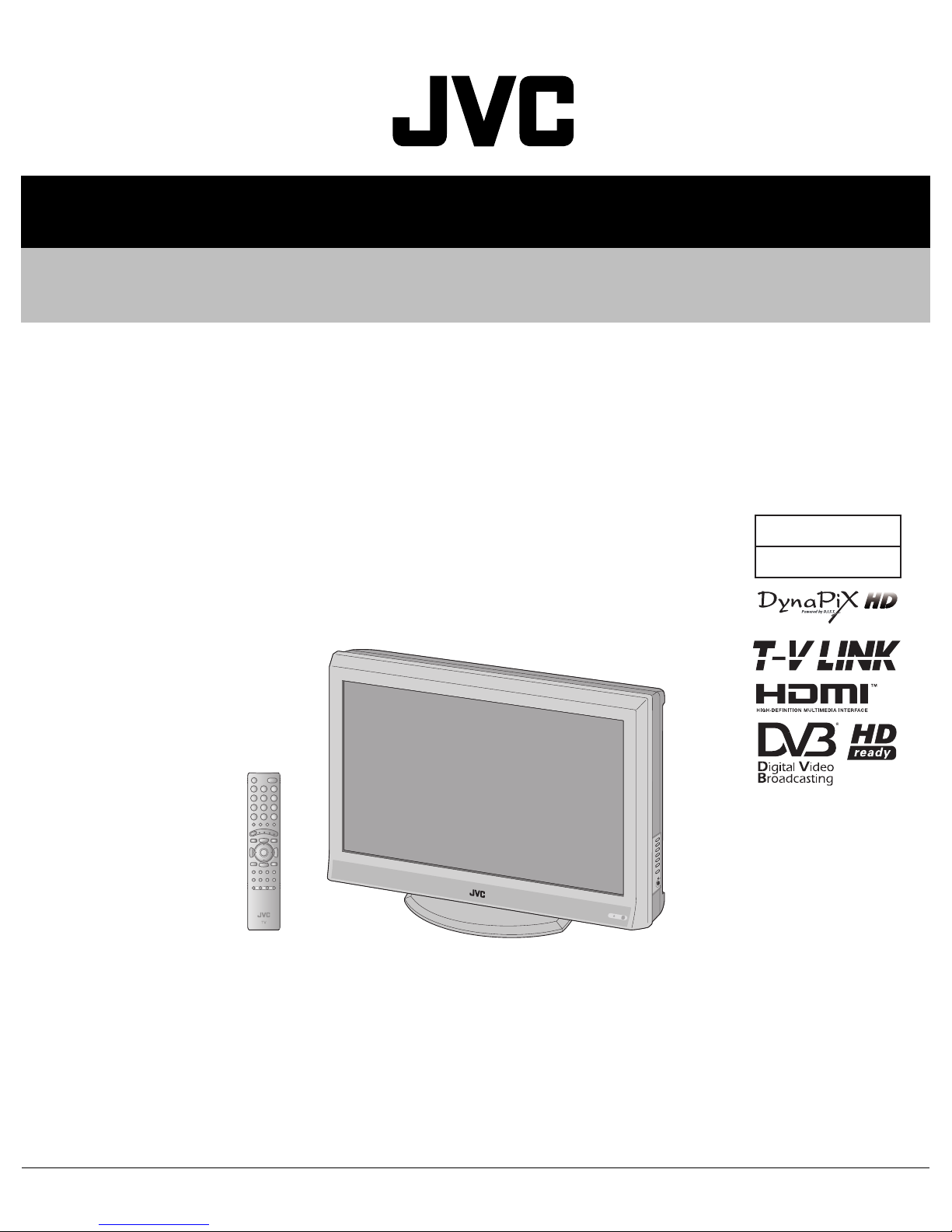
LCD INTEGRATED DIGITAL TELEVISION
YA40820063
LT-26DR7BJ, LT-26DR7BJ/P, LT-26DR7SJ,
LT-26DR7SJ
/P, LT-32DR7BJ, LT-32DR7BJ/P,
LT-32DR7SJ, LT-32DR7SJ/P,LT-37DR7BJ,
LT-37DR7BJ/P, LT-37DR7SJ, LT-37DR7SJ/P
BASIC CHASSIS
FL3
1 PRECAUTION. . . . . . . . . . . . . . . . . . . . . . . . . . . . . . . . . . . . . . . . . . . . . . . . . . . . . . . . . . . . . . . . . . . . . . . . . 1-3
2 SPECIFIC SERVICE INSTRUCTIONS . . . . . . . . . . . . . . . . . . . . . . . . . . . . . . . . . . . . . . . . . . . . . . . . . . . . . . 1-6
3 DISASSEMBLY . . . . . . . . . . . . . . . . . . . . . . . . . . . . . . . . . . . . . . . . . . . . . . . . . . . . . . . . . . . . . . . . . . . . . . 1-10
4 ADJUSTMENT . . . . . . . . . . . . . . . . . . . . . . . . . . . . . . . . . . . . . . . . . . . . . . . . . . . . . . . . . . . . . . . . . . . . . . . 1-19
5 TROUBLESHOOTING . . . . . . . . . . . . . . . . . . . . . . . . . . . . . . . . . . . . . . . . . . . . . . . . . . . . . . . . . . . . . . . . . 1-24
COPYRIGHT © 2006 Victor Company of Japan, Limited
TABLE OF CONTENTS
No.YA408
2006/5
Page 2
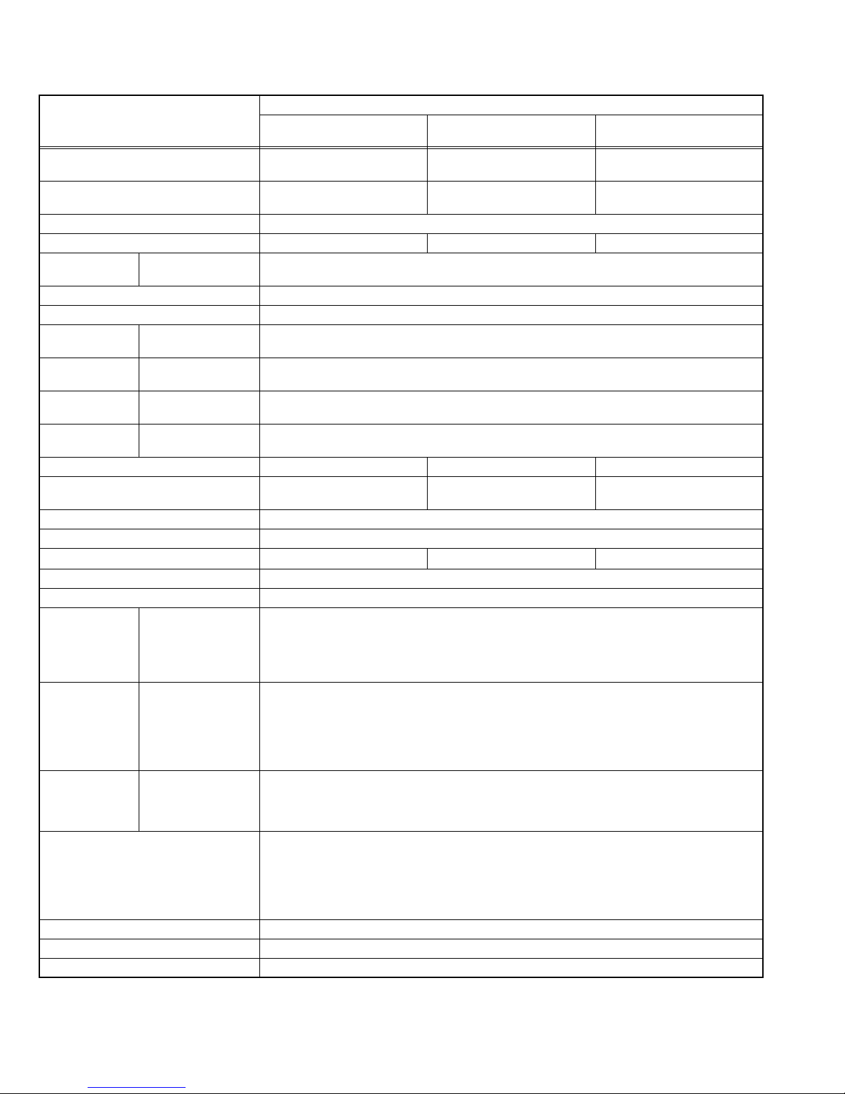
SPECIFICATION
Contents
Items
Dimensions ( W × H × D )
Mass 14.9 kg [Included stand]
Power Input AC220V - AC240 V, 50 Hz
Power Consumption 113 W (Standby: 0.6 W) 136 W (Standby: 0.6 W) 162 W (Standby: 0.5 W)
TV RF System Analog
Colour System PAL, NTSC 3.58/4.43 [EXT only]
Stereo System NICAM ( I )
Receiving
Frequency
Intermediate
Frequency
Colour Sub
Carrier Frequency
Teletext System Analog
LCD panel 26V-inch wide aspect (16 : 9) 32V-inch wide aspect (16 : 9) 37V-inch wide aspect (16 : 9)
Screen Size Diagonal : 66 cm
Display Pixels Horizontal : 1366 dots × Vertical : 768 dots (W-XGA)
Audio Power Output 10 W + 10 W
Speaker
Aerial terminal (VHF/UHF) 75 Ω unbalanced, coaxial
EXT-1 / EXT-2 (Input / Output) 21-pin Euro connector (SCART socket ) × 2
EXT-3 (Input) S-Video
EXT-4 (Input) Component Video
750p / 1125i
625p / 525p / 625i / 525i
EXT-5
(HDMI Input)
PC (RGB) Input D-sub 15 pin × 1
Audio output 500 mV (rms), Low impedance, RCA pin jack × 2
Headphone 3.5 mm stereo mini jack × 1
Remote Control Unit RM-C1905S (AAA/R03 dry cell battery × 2)
67.2 cm × 51.7 cm × 24.4 cm [Included stand]
67.2 cm
13.0 kg [TV only]
CCIR (I)
Digital
DVB-T
Analog
UHF: 470 MHz - 862 MHz
Digital
UHF: 474 MHz - 850 MHz
VIF
38.9MHz ( I )
SIF
32.9MHz (6.0MHz :I)
PAL
4.43MHz
NTSC
3.58MHz / 4.43MHz
FLOF (Fastext level 2.5), WST(World Standard system)
Digital
MHEG 5 UK profile
(H: 57.6 cm × V: 32.4 cm)
5 cm × 12 cm, Oval type × 2 5.5 cm × 15 cm, Oval type × 2
Mini-DIN 4 pin × 1
Y: 1 V (p-p), Positive (Negative sync provided), 75 Ω
C: 0.286 V (p-p) (Burst signal), 75 Ω
1 V (p-p), Positive (Negative sync provided), 75 Ω, RCA pin jack × 1
Video
500 mV (rms), High impedance, RCA pin jack × 2
Audio
RCA pin jack × 3
Y : 1 V (p-p) (Sync signal: ±0.35V(p-p), 3-value sync.), 75Ω
Pb/Pr : ±0.35V(p-p), 75 Ω
Y : 1 V (p-p), Positive (Negative sync provided), 75 Ω
Cb/Cr : 0.7V(p-p), 75 Ω
500 mV(rms) (-4dBs), high impedance, RCA pin jack × 2
Audio
Video
HDMI 2-row 19pin connector × 1
(Digital-input terminal is not compatible with picture signals of personal computer)
Digital: HDMI 2-row 19pin connector × 1
Audio
Anarog: 500mV(rms) (-4dBs), high impedance, RCA pin jack × 2
R/G/B : 0.7 V (p-p), 75Ω
HD / VD : 1 V (p-p) to 5 V (p-p), high impedance
< Available signal >
VGA : 640 pixels × 480 pixels (Horizontal : 31.5 kHz / Vertical : 60 Hz)
XGA : 1024 pixels × 768 pixels (Horizontal : 48.4 kHz / Vertical : 60 Hz)
Design & specifications are subject to change without notice.
LT-26DR7BJ
LT-26DR7SJ
×
47.1 cm × 137.7 cm [TV only]
LT-32DR7BJ
LT-32DR7SJ
×
59.1 cm × 24.4 cm [Included stand]
80.0 cm
80.0 cm
×
54.5 cm × 137.8 cm [TV only]
17.9 kg [Included stand]
16.0 kg [TV only]
Diagonal : 80 cm
(H: 69.7 cm × V: 39.2 cm)
LT-37DX7BJ
LT-37DX7SJ
×
64.9 cm × 31.1 cm [Included stand]
91.9 cm
91.9 cm
×
60.3 cm × 12.8 cm [TV only]
23.2 kg [Included stand]
20.3 kg [TV only]
Diagonal : 94 cm
(H: 82.6 cm × V: 46.1 cm)
4 cm × 16 cm
, Oval type × 2
1-2 (No.YA408)
Page 3

SECTION 1
PRECAUTION
1.1 SAFETY PRECAUTIONS
(1) The design of this product contains special hardware and many circuits and components specially for safety purposes. For
continued protection, no changes should be made to the original design unless authorized in writing by the manufacturer.
Replacement parts must be identical to those used in the original circuits. Service should be performed by qualified personnel
only.
(2) Alterations of the design or circuitry of the product should not be made. Any design alterations or additions will void the
manufacturer's warranty and will further relieve the manufacturer of responsibility for personal injury or property damage
resulting therefrom.
(3) Many electrical and mechanical parts in the product have special safety-related characteristics. These characteristics are often
not evident from visual inspection nor can the protection afforded by them necessary be obtained by using replacement
components rated for higher voltage, wattage, etc. Replacement parts which have these special safety characteristics are
identified in the Parts List of Service Manual. Electrical components having such features are identified by shading on the
schematics and by ( ) on the Parts List in the Service Manual. The use of a substitute replacement which does not have the
same safety characteristics as the recommended replacement part shown in the Parts List of Service Manual may cause shock,
fire, or other hazards.
(4) The leads in the products are routed and dressed with ties, clamps, tubing’s, barriers and the like to be separated from live parts,
high temperature parts, moving parts and / or sharp edges for the prevention of electric shock and fire hazard. When service is
required, the original lead routing and dress should be observed, and it should be confirmed that they have been returned to
normal, after re-assembling.
WARNING
(1) The equipment has been designed and manufactured to meet international safety standards.
(2) It is the legal responsibility of the repairer to ensure that these safety standards are maintained.
(3) Repairs must be made in accordance with the relevant safety standards.
(4) It is essential that safety critical components are replaced by approved parts.
(5) If mains voltage selector is provided, check setting for local voltage.
(No.YA408)1-3
Page 4
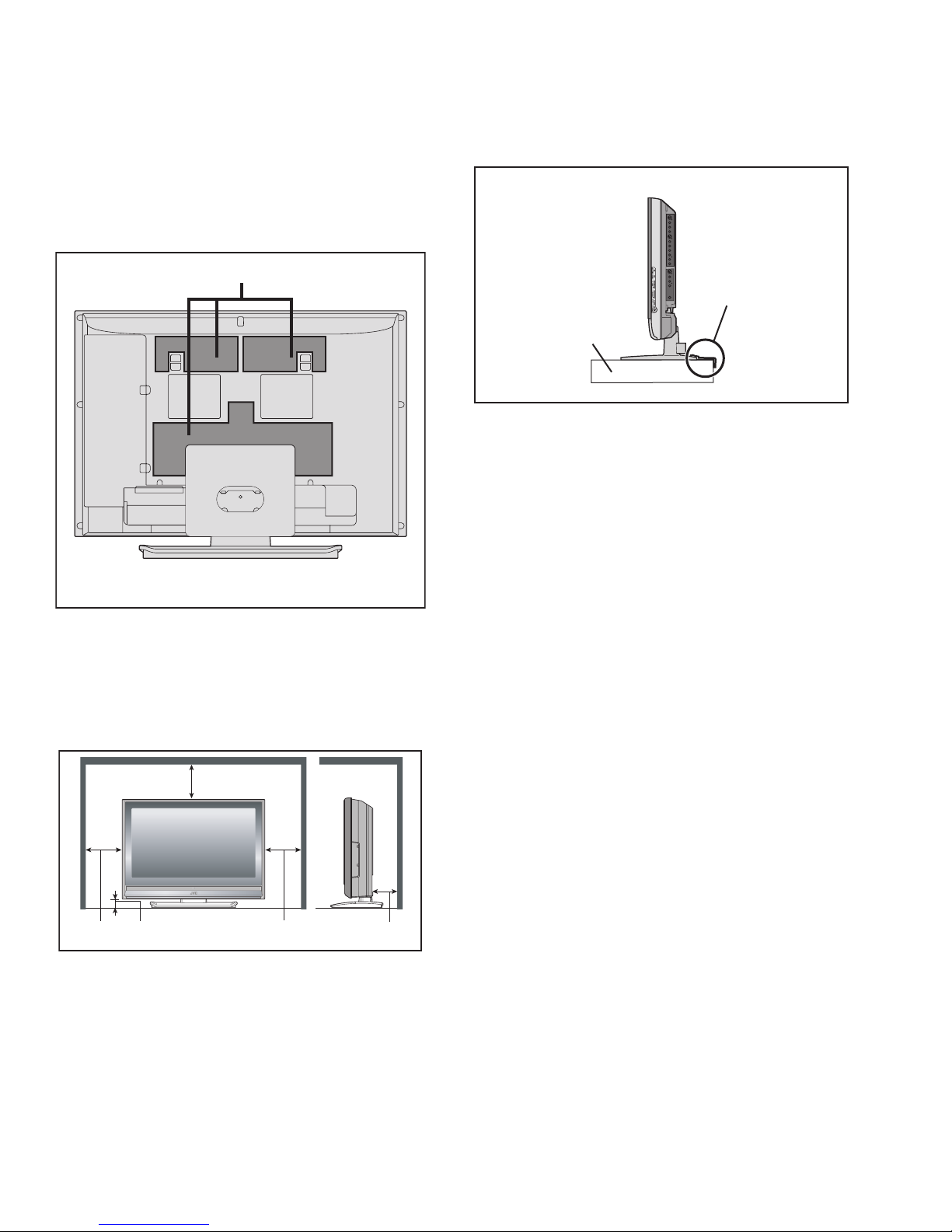
1.2 INSTALLATION
1.2.1 HEAT DISSIPATION
If the heat dissipation vent behind this unit is blocked, cooling
efficiency may deteriorate and temperature inside the unit will
rise. The temperature sensor that protects the unit will be
activated when internal temperature exceeds the pre-determined
level and power will be turned off automatically.Therefore,
please make sure pay attention not to block the heat dissipation
vent as well as the ventilation outlet behind the unit and ensure
that there is room for ventilation around it.
Ventilation hole
*Diagram differs from actual appearance.
1.2.3 INSTALLATION REQUIREMENTS
To ensure safety in an emergency such as an earthquake, and
to prevent accidents, ensure that measures are taken to prevent
the TV dropping or falling over.
< SIDE VIEW >
It fixes in a band.
TV STAND
*Diagram differs from actual appearance.
1.2.4 NOTES ON HANDLING
(1) WHEN TAKING UNIT OUT OF A PACKING CASE
When taking the unit out of a packing case, do not grasp
the upper part of the unit. If you take the unit out while
grasping the upper part, the LCD PANEL may be damaged
because of a pressure. Instead of grasping the upper part,
put your hands on the lower backside or sides of the unit.
(2) AS FOR PRESSING OR TOUCHING A SPEAKER
Be careful not to press the opening of the speaker in the
lower part of the unit and around them since the decorative
sheet on the surface of the openings may be deformed.
1.2.2 INSTALLATION REQUIREMENTS
Ensure that the minimal distance is maintained, as specified
below, between the unit with and the surrounding walls, as well
as the floor etc.Install the unit on stable flooring or stands.Take
precautionary measures to prevent the unit from tipping in order
to protect against accidents and earthquakes.
200mm
*Diagram differs from actual appearance.
50mm150mm 150mm 50mm
1-4 (No.YA408)
Page 5

1.3 HANDLING LCD PANEL
1.3.1 PRECAUTIONS FOR TRANSPORTATION
When transporting the unit, pressure exerted on the internal LCD
panel due to improper handling (such as tossing and dropping)
may cause damages even when the unit is carefully packed. To
prevent accidents from occurring during transportation, pay
careful attention before delivery, such as through explaining the
handling instructions to transporters.
Ensure that the following requirements are met during
transportation, as the LCD panel of this unit is made of glass and
therefore fragile:
(1) USE A SPECIAL PACKING CASE FOR THE LCD PANEL
When transporting the LCD panel of the unit, use a special
packing case (packing materials). A special packing case
is used when a LCD panel is supplied as a service spare
part.
(2) ATTACH PROTECTION SHEET TO THE FRONT
Since the front (display part) of the panel is vulnerable,
attach the protection sheet to the front of the LCD panel
before transportation. Protection sheet is used when a LCD
panel is supplied as a service spare part.
(3) AVOID VIBRATIONS AND IMPACTS
The unit may be broken if it is toppled sideways even when
properly packed. Continuous vibration may shift the gap of
the panel, and the unit may not be able to display images
properly. Ensure that the unit is carried by at least 2
persons and pay careful attention not to exert any vibration
or impact on it.
(4) DO NOT PLACE EQUIPMENT HORIZONTALLY
Ensure that it is placed upright and not horizontally during
transportation and storage as the LCD panel is very
vulnerable to lateral impacts and may break. During
transportation, ensure that the unit is loaded along the
traveling direction of the vehicle, and avoid stacking them
on one another. For storage, ensure that they are stacked
in 2 layers or less even when placed upright.
1.3.2 OPTICAL FILTER (ON THE FRONT OF THE LCD PANEL)
(1) Avoid placing the unit under direct sunlight over a
prolonged period of time. This may cause the optical filter
to deteriorate in quality and COLOUR.
(2) Clean the filter surface by wiping it softly and lightly with a
soft and lightly fuzz cloth (such as outing flannel).
(3) Do not use solvents such as benzene or thinner to wipe the
filter surface. This may cause the filter to deteriorate in
quality or the coating on the surface to come off. When
cleaning the filter, usually use the neutral detergent diluted
with water. When cleaning the dirty filter, use water-diluted
ethanol.
(4) Since the filter surface is fragile, do not scratch or hit it with
hard materials. Be careful enough not to touch the front
surface, especially when taking the unit out of the packing
case or during transportation.
1.3.3 PRECAUTIONS FOR REPLACEMENT OF EXTERIOR
PARTS
Take note of the following when replacing exterior parts (REAR
COVER, FRONT PANEL, etc.):
(1) Do not exert pressure on the front of the LCD panel (filter
surface). It may cause irregular COLOUR.
(2) Pay careful attention not to scratch or stain the front of the
LCD panel (filter surface) with hands.
(3) When replacing exterior parts, the front (LCD panel) should
be placed facing downward. Place a mat, etc. underneath
to avoid causing scratches to the front (filter surface).
(No.YA408)1-5
Page 6
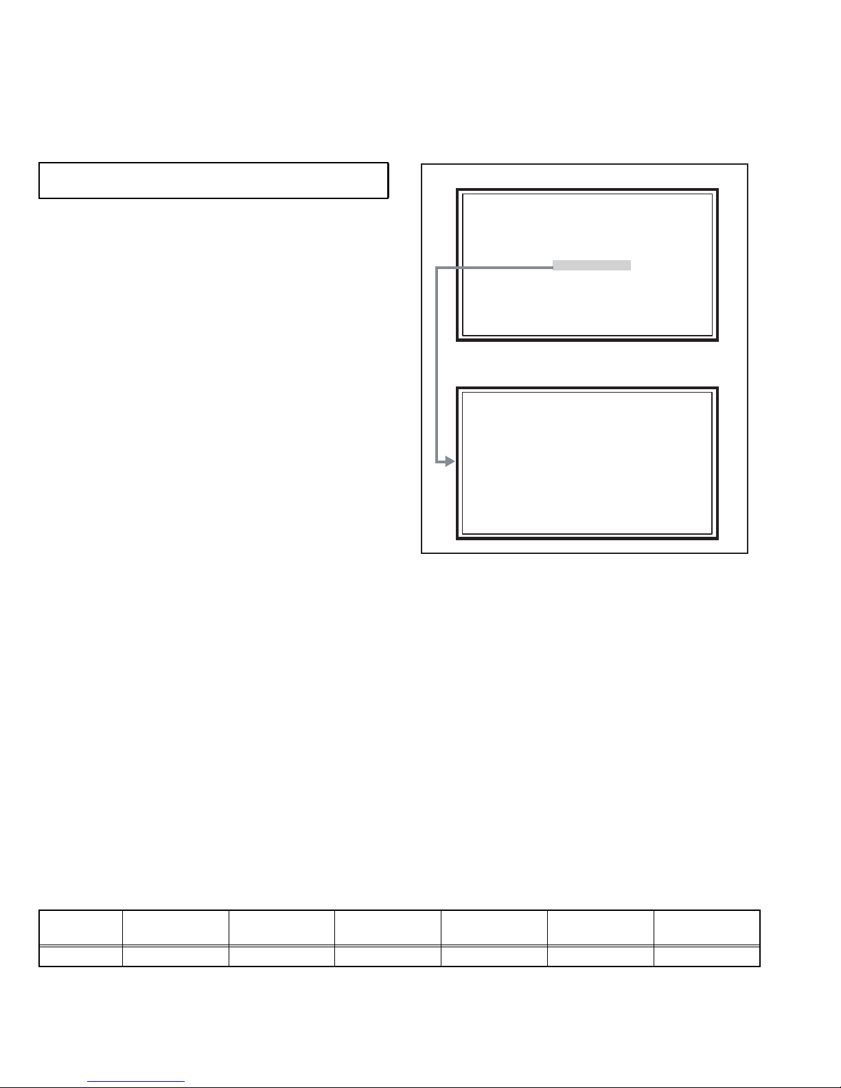
2.1 SYSTEM SETTEING
SERVICE MENU
1. ADJUST
2. SELF CHECK
3. I2C STOP
LOB 0 FAN 0
AUD 0
ANA 9 DIG 9
0000 00
00
SECTION 2
SPECIFIC SERVICE INSTRUCTIONS
Be sure to carry out the following operation at the end of
the procedure.
(1) Press the [INFORMATION] key and [MUTING] key
simultaneously, then enter the SERVICE MODE.
(2) When the Main Menu is displayed, press [2] key to enter
the self check mode.
(3) Turn off the power by pressing the [POWER] key on the
remote control unit.
SERVICE MENU SCREEN
SERVICE MENU
1. ADJUST
2. SELF CHECK
3. I2C STOP
SELF CHECK MODE SCREEN
LOB 0 FAN 0
AUD 0
ANA 9 DIG 9
0000 00
00
2.2 FEATURES
DVB-T
This TV can receive both DVB-T (Digital terrestrial broadcasting)
and Analogue terrestrial broadcasting.
D.I.S.T. (Digital Image Scaling Technology)
This system uses line interpolation to double the number of
scanning lines and achieve high resolution, flicker-free picture.
Colour Management
This function ensures dull colours are compensated to
produce natural hues.
Picture Management
This function makes it easier to see the dark areas when a
picture has many dark areas, and makes it easier to see the
bright areas when a picture has many bright areas.
Smart Picture
This function detects the APL (Average Picture Level) and
adjusts the contrast suitable for what you are watching.
DIGITAL VNR
This function cuts down the amount of noise in the original
picture.
MPEG Noise Reduction
This function effects the block noise removal and mosquito NR
simultaneously.
3D Cinema Sound
You can enjoy sounds with a widerambience.
2.3 MAIN DIFFERENCE LIST
Item
LT-26DR7BJ
LT-26DR7BJ/P
LT-26DR7SJ
LT-26DR7SJ/P
LT-32DR7BJ
LT-32DR7BJ/P
LT-32DR7SJ
LT-32DR7SJ/P
LT-32DR7BJ
LT-32DR7BJ/P
Paint colour Silver & Black Silver Silver & Black Silver Silver & Black Silver
1-6 (No.YA408)
LT-32DR7SJ
LT-32DR7SJ/P
Page 7
2.4 HOW TO IDENTIFY MODELS
Except "/P" models : "AE" is added to the serial No. after at the Rating label.
"/P" models : "PE" is added to the serial No. after at the Rating label.
MODEL No.
LT-26DR7BJ
LT-32DR7BJ
LT-37DR7BJ
LT-26DR7SJ
LT-32DR7SJ
LT-37DR7SJ
AE
SERIAL NO.
PE
Indicated
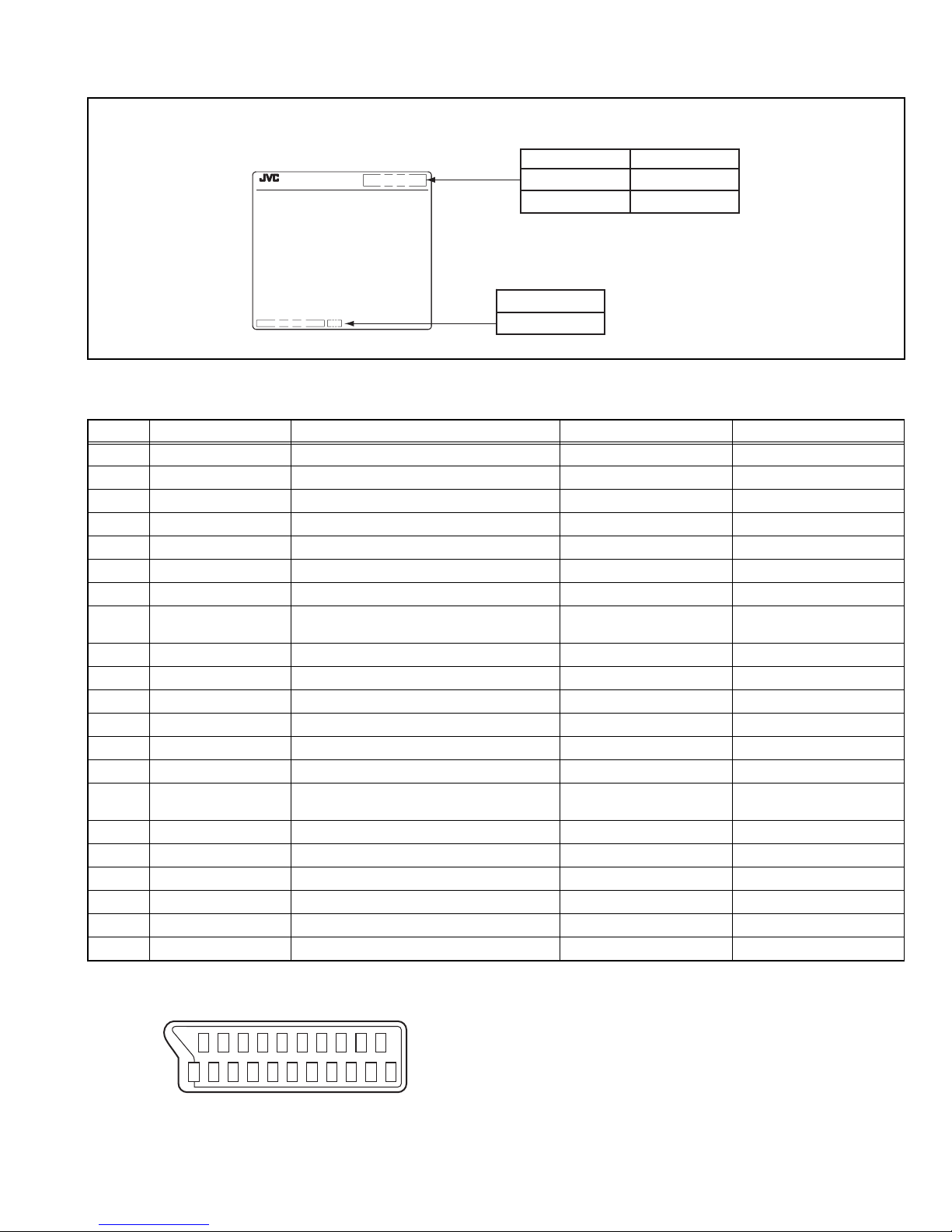
2.5 21-PIN EURO CONNECTOR (SCART) : EXT-1 / EXT-2
Pin No. Signal designation Matching value EXT-1 EXT-2
1 AUDIO R output 500mV(rms) (Nominal), Low impedance Used (TV OUT) Used (LINE OUT)
2 AUDIO R input 500mV(rms) (Nominal), High impedance Used (R1) Used (R2)
3 AUDIO L output 500mV(rms) (Nominal), Low impedance Used (TV OUT) Used (LINE OUT)
4 AUDIO GND Used Used
5 GND (B) Used Used
6 AUDIO L input 500mV(rms) (Nominal), High impedance Used (L1) Used (L2)
7 B input 700mV
8 FUNCTION SW
(SLOW SW)
Low : 0V-3V
High : 8V-12V, High impedance
, 75Ω Used Used
(B-W)
Used Used
9 GND (G) Used Used
10 SCL / T-V LINK Not used Used (SCL2 / TV-LINK)
11 G input 700mV
, 75Ω Used Used
(B-W)
12 SDA Not used Used (SDA2)
13 GND (R) Used Used
14 GND (YS) Used Not used
15 R / C input R : 700mV
C : 300mV
(B-W)
(P-P)
, 75Ω
, 75Ω
Used (R) Used (C2/R)
16 Ys input (FAST SW) Low : 0V-0.4V, High : 1V-3V, 75Ω Used Used
17 GND (VIDEO output) Used Used
18 GND (VIDEO input) Used Used
19 VIDEO output 1V
20 VIDEO / Y input 1V
(Negative sync), 75Ω Used (TV OUT) Used (LINE OUT)
(P-P)
(Negative sync), 75Ω Used Used
(P-P)
21 COMMON GND Used Used
(P-P= Peak to Peak, B-W= Blanking to white peak)
[Pin assignment]
20 18 16 14 12 10 8 6 4 2
21 19 17 15 13 11 9 7 5 3 1
(No.YA408)1-7
Page 8
2.6 TECHNICAL INFORMATION
2.6.1 LCD PANEL
This unit uses the flat type panel LCD (Liquid Crystal Display) panel that occupies as little space as possible, instead of the
conventional CRT (Cathode Ray Tube), as a display unit.
Since the unit has the two polarizing filter that are at right angles to each other, the unit adopts "normally black" mode, where light
does not pass through the polarizing filter and the screen is black when no voltage is applied to the liquid crystals.
2.6.1.1 SPECIFICATIONS
The following table shows the specifications of this unit.
Item
Maximum dimensions ( W × H × D )
26V LCD PANEL UNIT 32V LCD PANEL UNIT 37V LCD PANEL UNIT
626 mm × 373 mm × 44.1 mm 760 mm × 450 mm × 48 mm 877 mm × 516.8 mm × 55.5 mm
Specifications
Weight 5.0 kg 6.9 kg 10.5 kg
Effective screen size Diagonal: 660 mm
(H: 576 mm × V: 324 mm)
Diagonal: 800 mm
(H: 697 mm × V: 392 mm)
Diagonal: 940 mm
(H: 820 mm × V: 461 mm)
Aspect ratio 16 : 9
Drive device / system a-Si-TFT active matrix system
Resolution Horizontally 1366 × Vertically 768 × RGB < W-XGA > 3147264 dots in total
Pixel pitch (pixel size) Horizontally: 0.1405 mm
Vertically: 0.4215 mm
Horizontally: 0.1703 mm
Vertically: 0.5108 mm
Horizontally: 0.2 mm
Vertically: 0.6 mm
Displayed colour 16777216 colours 256 colours for R G and B
Brightness 500cd/m2
Contrast ratio 700 : 1 800 : 1
Response time (Tr + Tf) less than 18 ms
View angle (Horizontally) 178°
View angle (Vertically) 178°
Surface polarizer Anti-Glare type Low reflective coat
Colour filter Vertical stripe
Backlight
Cold cathode fluorescent lamp ×17 Cold cathode fluorescent lamp ×18 Cold cathode fluorescent lamp × 20
Power supply voltage in LCD 12 V
Power supply voltage in inverter
24 V
Panel interface system LVDS (Low Voltage Differential Signaling)
2.6.1.2 PIXEL FAULT
There are three pixel faults - bright fault , dark fault and flicker fault - that are respectively defined as follows.
BRIGHT FAULT
In this pixel fault, a cell that should not light originally is lighting on and off.
For checking this pixel fault, input ALL BLACK SCREEN and find out the cell that is lighting on and off.
DARK FAULT
In this pixel fault, a cell that should light originally is not lighting or lighting with the brightness twice as brighter as originally lighting.
For checking this pixel fault, input 100% of each R/G/B colour and find out the cell that is not lighting.
FLICKER FAULT
In the pixel fault, a cell that should light originally or not light originally is flashing on and off.
For checking this pixel fault, input ALL BLACK SCREEN signal or 100% of each RGB colour and find out the cell that is flashing on
and off.
1-8 (No.YA408)
Page 9

2.6.2 MAIN CPU PIN FUNCTION [IC7301
Pin Pin name I/O Function Pin Pin name I/O Function
1 TCK O Test purpose 65 D2 I/O Program ROM data for main CPU
2 TMS I Test purpose 66 D12 I/O Program ROM data for main CPU
3 TDI I Test purpose 67 D10 I/O Program ROM data for main CPU
4 TDO O Test purpose 68 VSS33 - GND
5 P2.8 O TV, Subtitle/OTHER 69 VDD33 I 3.3V
6 P2.9 O Blue for OSD 70 D4 I/O Program ROM data for main CPU
7 P2.10 O Blue for OSD 71 D3 I/O Program ROM data for main CPU
8 P2.11 O Blue for OSD 72 D11 I/O Program ROM data for main CPU
9 P2.12 O Blue for OSD 73 RSTIN I Reset
10 P2.13 O Blue for OSD 74 POWER O Sleep state release for chassis CPU [Relese : L]
11 P2.14 I TV-LINK 75 P3.1 O DM_RESET(IDTV)
12 P2.15 O Request for chassis CPU communication 76 REMOCON I Remote control
13 VSS33 - GND 77 P3.3 I Clock for OSD
14 VDD33 I 3.3V 78 P3.4 O Red for OSD
15 P4.5 O TV-LINK out 79 P3.5 O Red for OSD
16 A20 O Program ROM address for main CPU 80 P3.6 O Red for OSD
17 A19 O Program ROM address for main CPU 81 P3.7 O Red for OSD
18 A18 O Program ROM address for main CPU 82 MTST I/O Data transmission for chassis CPU communication
19 A17 O Program ROM address for main CPU 83 MTSR I/O Data receive for chassis CPU communication
20 VSS25 - GND 84 VSS33 - GND
21 VDD25 I 2.5V 85 VDD33 I 3.3V
22 A16 O Program ROM address for main CPU 86 VSS25 - GND
23 A8 O Program ROM address for main CPU 87 VDD25 I 2.5V
24 A7 O Program ROM address for main CPU 88 TXD0 I/O Communication for adjustment
25 A9 O Program ROM address for main CPU 89 RXD0 I/O Communication for adjustment
26 A6 O Program ROM address for main CPU 90 P3.12 O Red for OSD
27 A5 O Program ROM address for main CPU 91 CLK O Clock for chassis CPU communication
28 A10 O Program ROM address for main CPU 92 P3.15 O Green for OSD
29 A11 O Program ROM address for main CPU 93 P5.14 O Green for OSD
30 A12 O Program ROM address for main CPU 94 P5.15 O Green for OSD
31 VSS33 - GND 95 TRIG_IN O Green for OSD
32 VDD33 I 3.3V 96 TRIG_OUT O Green for OSD
33 A4 O Program ROM address for main CPU 97 P6.2 O Green for OSD
34 A3 O Program ROM address for main CPU 98 P6.3 I/O I
35 A2 O Program ROM address for main CPU 99 P6.4 I/O I
36 A1 O Program ROM address for main CPU 100 P6.5 O Teletext signal select [Analog RGB : H / Digital RGB : L]
37 A0 O Program ROM address for main CPU 101 IRQ O IRQ(IDTV)
38 A13 O Program ROM address for main CPU 102 VSYNC I/O Vertical sync
39 ARAS/A14 O Program ROM address for main CPU 103 HSYNC I/O Horizontal sync
40 CAS/A15 O Program ROM address for main CPU 104
41 VSS33 - GND 105 BLANK O Ys for OSD / Teletext
42 VDD33 I 3.3V 106 VDD33 I 3.3V
43 MEMCLK O Clock for memory 107 VSS33 - GND
44 CSSDRAM O Chip select for memory 108 XTAL1 I 6MHz for system clock
45 CLKEN O Clock enable for memory 109 XTAL2 O 6MHz for system clock
46 CSROM O Chip select for memory 110 VSSA - GND
47 RD O Read for memory 111 VDDA I 2.5V
48 UDQM O Control buffer of memory 112 R O R for OSD / Teletext
49 LDQM O Control buffer of memory 113 G O G for OSD / Teletext
50 WR O Write for memory 114 B O B for OSD / Teletext
51 D15 I/O Program ROM data for main CPU 115 VSSA - GND
52 VSS33 - GND 116 VDDA I 2.5V
53 VDD33 I 3.3V 117 CVBS2 I Video for Teletext
54 D7 I/O Program ROM data for main CPU 118 VSSA - GND
55 D0 I/O Program ROM data for main CPU 119 VDDA I 2.5V
56 D14 I/O Program ROM data for main CPU 120 CVBS1B I Video for Teletext
57 D8 I/O Program ROM data for main CPU 121 CVBS1A I Video for Teletext
58 D6 I/O Program ROM data for main CPU 122 VSSA - GND
59 D1 I/O Program ROM data for main CPU 123 VDDA I 2.5V
60 VSS33 - GND 124 KEY1 I Key scan data 1 [ON : H]
61 VDD33 I 3.3V 125 KEY2 I Key scan data 2 [ON : H]
62 D13 I/O Program ROM data for main CPU 126 MECA_SW I Main power ON / OFF control [ON : L]
63 D9 I/O Program ROM data for main CPU 127
64 D5 I/O Program ROM data for main CPU 128 TMODE I Test purpose
: DIGITAL PWB]
COR/RSTOUT
(KEYP2)P5.3
2
C bus clock (for main memory)
2
C bus Data (for main memory)
O Not used
I Not used
(No.YA408)1-9
Page 10

SECTION 3
DISASSEMBLY
3.1 CAUTION AT DISASSEMBLY
• Be sure to perform the SYSTEM SETTEING, at the end of the procedure.
• Make sure that the power cord is disconnected from the outlet.
• Pay special attention not to break or damage the parts.
• When removing each board, remove the connectors as required. Taking notes of the connecting points (connector numbers) makes
service procedure manageable.
• Make sure that there is no bent or stain on the connectors before inserting, and firmly insert the connectors.
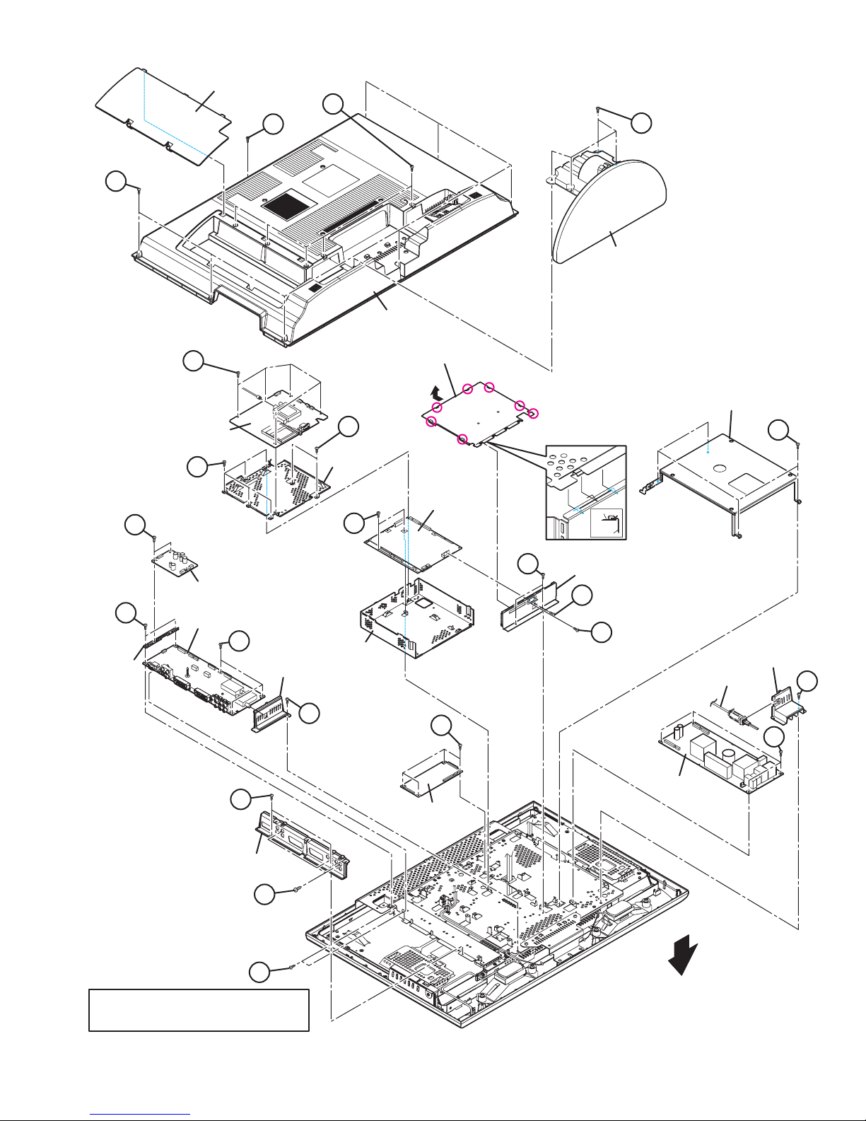
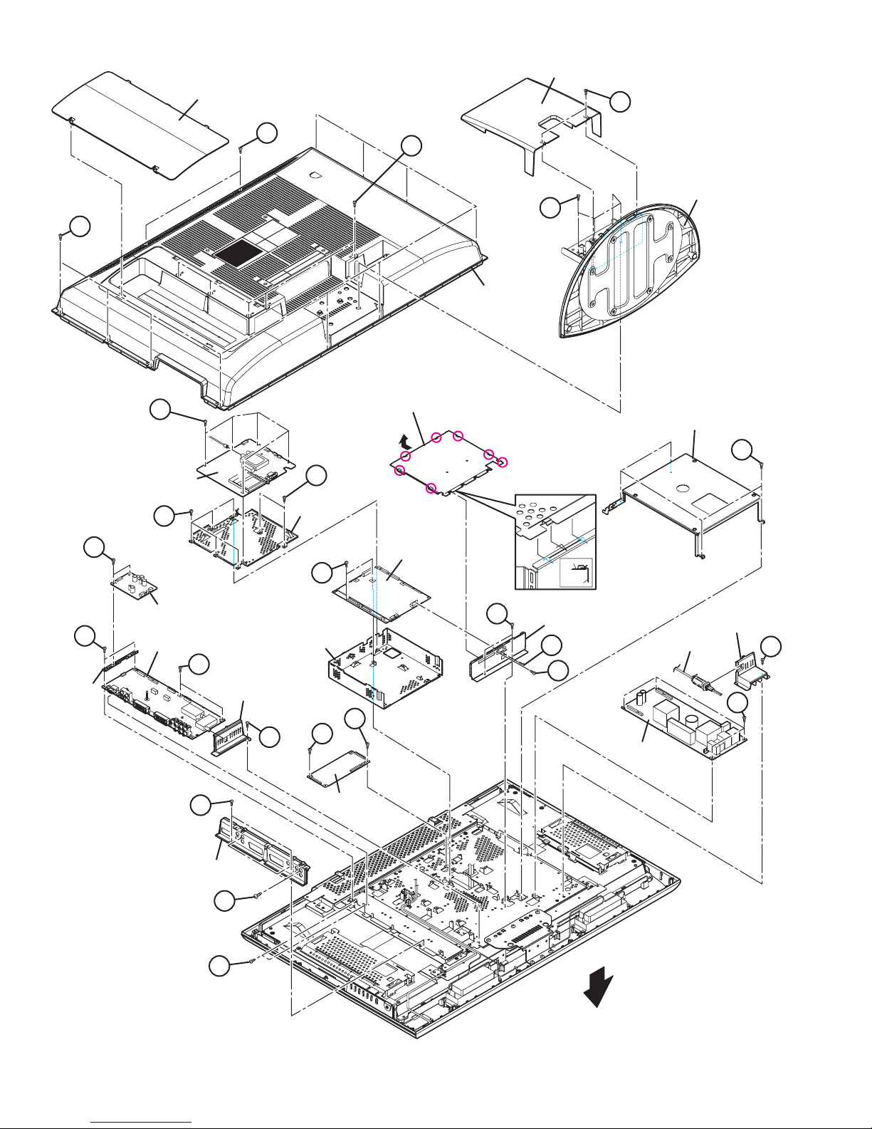
3.2 DISASSEMBLY PROCEDURE [26 inch models and 32 inch models]
3.2.1 REMOVING THE STAND (Fig.1)
(1) Remove the 4 screws [A].
(2) Remove the STAND.
3.2.2 REMOVING THE REAR COVER (Fig.1)
• Remove the STAND.
(1) Remove the JACK COVER (L/R).
(2) Remove the 7 screws [B], the 5 screws [C], and the 1
screw [D].
(3) Remove the REAR COVER.
3.2.3 REMOVING THE POWER PWB (Fig.1)
• Remove the STAND.
• Remove the REAR COVER.
(1) Remove the 1 screw [E].
(2) Remove the POWER CORD HOLDER.
(3) Remove the POWER CORD from the POWER PWB.
(4) Remove the 4 screws [F].
(5) Remove the POWER PWB.
3.2.4 REMOVING THE D-AMP PWB (Fig.1)
• Remove the STAND.
• Remove the REAR COVER.
(1) Remove the 2 screw [G].
(2) Remove the D-AMP PWB.
3.2.5 REMOVING THE ANALOG PWB (Fig.1)
• Remove the STAND.
• Remove the REAR COVER.
• Remove the D-AMP PWB.
(1) Remove the 3 screws [H] and 2 screws [J].
(2) Remove the TERMINAL BASE.
(3) Remove the 1 screw [K].
(4) Remove the TUNER BASE.
(5) Remove the 2 screws [L].
(6) Remove the D-AMP BRACKET.
(7) Remove the 3 screws [M] and 2 screws [N].
(8) Remove the ANALOG PWB.
3.2.6 REMOVING THE DC-DC PWB (Fig.1)
• Remove the STAND.
• Remove the REAR COVER.
(1) Remove the 4 screws [P].
(2) Remove the BACK BRACKET.
(3) Remove the 4 screws [Q].
(4) Remove the DC-DC PWB.
3.2.7 REMOVING THE DIGITAL TUNER UNIT (Fig.1)
• Remove the STAND.
• Remove the REAR COVER.
• Remove the BACK BRACKET.
(1) Remove the 7 hooks of the SHIELD COVER.
(2) Remove the SHIELD COVER by sliding it in the direction of
the arrow.
(3) Remove the 5 screws [R] and 2 screws [S].
(4) Remove the DIGITAL TUNER UNIT.
3.2.8 REMOVING THE DIGITAL PWB (Fig.1)
• Remove the STAND.
• Remove the REAR COVER.
• Remove the BACK BRACKET.
• Remove the SHIELD COVER.
• Remove the DIGITAL TUNER UNIT.
(1) Remove the 2 screws [T] and 1 screw [U].
(2) Remove the SHIELD TERMINAL.
(3) Remove the 7 screws [V].
(4) Remove the DIGITAL PWB BRACKET.
(5) Remove the 2 screws [W].
(6) Remove the DIGITAL PWB.
CAUTION :
Make sure to perform the "SYSTEM SETTEING", when
DIGITAL PWB is replaced.
1-10 (No.YA408)
Page 11
JACK COVER
C
D
A
$
STAND
REAR COVER
L
D-AMP PWB
BRACKET
DIGITAL TUNER
UNIT
G
R
V
D-AMP PWB
ANALOG PWB
M
TUNER BASE
K
V
DIGITAL PWB
BRACKET
W
SHIELD BASE
SHIELD COVER
Hook
Hook
Hook
DIGITAL PWB
Q
Hook
Hook
Hook
Hook
T
SHIELD COVER
SHIELD TERMINAL
SHIELD TERMINAL
U
S
BACK BRACKET
POWER CORD HOLDER
POWER CORD
P
E
F
J
TERMINAL BASE
H
N
This exploded view shows the 32 inch models.
26 inch models have almost similar parts
locations.
POWER PWB
DC-DC PWB
FRONT
Fig.1
(No.YA408)1-11
Page 12
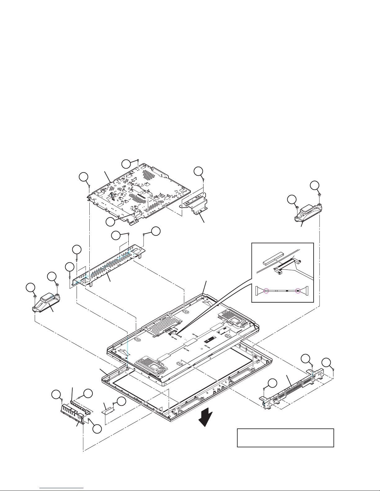
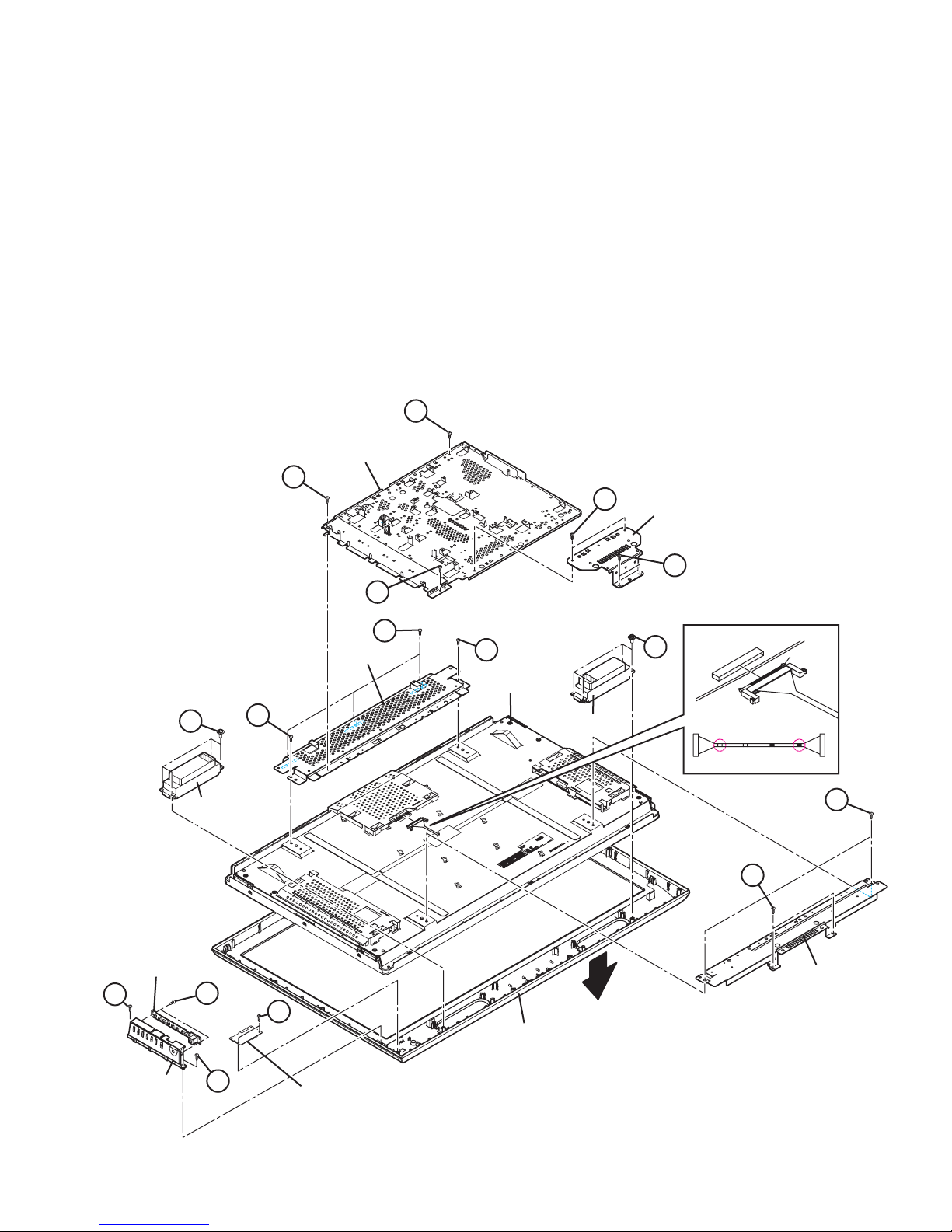
3.2.9 REMOVING THE SW PWB (Fig.2)
• Remove the STAND.
• Remove the REAR COVER.
(1) Remove the 2 screws [A].
(2) Remove the CONTROL ASS’Y with SW PWB.
(3) Remove the 2 screws [B].
(4) Remove the SW PWB from the CONTROL ASS’Y.
3.2.10 REMOVING THE LED PWB (Fig.2)
• Remove the STAND.
• Remove the REAR COVER.
(1) Remove the 2 screws [C].
(2) Remove the LED PWB.
3.2.11 REMOVING THE SPEAKER (Fig.2)
• Remove the STAND.
• Remove the REAR COVER.
(1) Remove the 4 screws [D].
(2) Remove the SPEAKER (L /R).
3.2.12 REMOVING THE LCD PANEL UNIT (Fig.2)
• Remove the STAND.
• Remove the REAR COVER.
• Remove the BACK BRACKET.
• Remove the POWER CORD HOLDER.
(1) Remove the 3 screws [E]. [26 inch models]
(2) Remove the 2 screws [E]. [32 inch models]
(3) Remove the STAND BRACKET.
(4) Remove the 3 screws [F].
(5) Remove the MAIN BASE.
(6) Remove the 4 screws [G] and 4 screw [H].
(7) Remove the LCD PANEL UNIT with TOP/BOTTOM
FRAME.
(8) Remove the 2 screws [J].
(9) Remove the TOP FARAME from the LCD PANEL UNIT.
(10) Remove the 2 screws [K].
(11) Remove the BOTTOM FARAME from the LCD PANEL
UNIT.
D
D
SPEAKER
MAIN BASE
F
E
F
D
D
F
G
J
G
STAND BRACKET
SPEAKER
The terminal of a connector is turned up and connects.
Surely insert and lock.
terminal side
J
LCD PANEL UNIT
TOP FRAME
Check that connector is inserted completly.
(Don't insert aslant)
"LVDS CABLE"
Black
white
LCD PANEL SIDE
white
Black
DIGITAL PWB SIDE
FRONT PANEL
SW PWB
A
CONTROL
ASS'Y
B
LED PWB
A
C
1-12 (No.YA408)
Fig.2
FRONT
K
BOTTOM FRAME
H
K
This exploded view shows the 32 inch models.
26 inch models have almost similar parts
locations.
Page 13

3.3 DISASSEMBLY PROCEDURE [37 inch models]
3.3.1 REMOVING THE STAND (Fig.3)
(1) Remove the 2 screws [A].
(2) Remove the STNAD COVER.
(3) Remove the 4 screws [B].
(4) Remove the STAND.
3.3.2 REMOVING THE REAR COVER (Fig.3)
• Remove the STAND.
(1) Remove the JACK COVER (L/R).
(2) Remove the 10 screws [C], the 5 screws [D], and the 2
screws [E].
(3) Remove the REAR COVER.
3.3.3 REMOVING THE POWER PWB (Fig.3)
• Remove the STAND.
• Remove the REAR COVER.
(1) Remove the 1 screw [F].
(2) Remove the POWER CORD HOLDER.
(3) Remove the POWER CORD.
(4) Remove the 4 screws [G].
(5) Remove the POWER PWB.
3.3.4 REMOVING THE D-AMP PWB (Fig.3)
• Remove the STAND.
• Remove the REAR COVER.
(1) Remove the 2 screw [H].
(2) Remove the D-AMP PWB.
3.3.5 REMOVING THE ANALOG PWB (Fig.3)
• Remove the STAND.
• Remove the REAR COVER.
• Remove the D-AMP PWB.
(1) Remove the 3 screws [J] and 2 screws [K].
(2) Remove the TERMINAL BASE.
(3) Remove the 1 screw [L].
(4) Remove the TUNER BASE.
(5) Remove the 2 screws [M].
(6) Remove the D-AMP BRACKET.
(7) Remove the 2 screws [N] and 2 screws [P].
(8) Remove the ANALOG PWB.
3.3.6 REMOVING THE DC-DC PWB (Fig.3)
• Remove the STAND.
• Remove the REAR COVER.
(1) Remove the 4 screws [Q].
(2) Remove the BACK BRACKET.
(3) Remove the 2 screws [R].
(4) Remove the DC-DC PWB.
3.3.7 REMOVING THE DIGITAL TUNER UNIT (Fig.1)
• Remove the STAND.
• Remove the REAR COVER.
• Remove the BACK BRACKET.
(1) Remove the 7 hooks of the SHIELD COVER.
(2) Remove the SHIELD COVER by sliding it in the direction of
the arrow.
(3) Remove the 5 screws [S] and 2 screws [T].
(4) Remove the DIGITAL TUNER UNIT.
3.3.8 REMOVING THE DIGITAL PWB (Fig.3)
• Remove the STAND.
• Remove the REAR COVER.
• Remove the BACK BRACKET.
• Remove the SHIELD COVER.
• Remove the DIGITAL TUNER UNIT.
(1) Remove the 2 screws [U] and 1 screw [V].
(2) Remove the SHIELD TERMINAL.
(3) Remove the 7 screws [W].
(4) Remove the DIGITAL PWB BRACKET.
(5) Remove the 2 screws [X].
(6) Remove the DIGITAL PWB.
CAUTION :
Make sure to perform the "SYSTEM SETTEING", when
DIGITAL PWB is replaced.
(No.YA408)1-13
Page 14
JACK COVER
STNAD COVER
A
㧯
S
DIGITAL TUNER
UNIT
W
E
W
DIGITAL PWB
BRACKET
D
SHIELD COVER
Hook
Hook
Hook
Hook
REAR COVER
Hook
Hook
STAND
B
BACK BRACKET
Q
Hook
M
D-AMP PWB
BRACKET
H
X
D-AMP PWB
ANALOG PWB
SHIELD BASE
N
TUNER BASE
DIGITAL PWB
U
SHIELD COVER
SHIELD TERMINAL
SHIELD TERMINAL
V
T
POWER CORD HOLDER
POWER CORD
F
G
R
L
K
TERMINAL BASE
R
POWER PWB
DC-DC PWB
J
P
1-14 (No.YA408)
FRONT
Fig.3
Page 15
3.3.9 REMOVING THE SW PWB (Fig.4)
• Remove the STAND.
• Remove the REAR COVER.
(1) Remove the 2 screws [A].
(2) Remove the CONTROL ASS’Y with SW PWB.
(3) Remove the 2 screws [B].
(4) Remove the SW PWB from the CONTROL ASS’Y.
3.3.10 REMOVING THE LED PWB (Fig.4)
• Remove the STAND.
• Remove the REAR COVER.
(1) Remove the 2 screws [C].
(2) Remove the LED PWB.
3.3.11 REMOVING THE SPEAKER (Fig.4)
• Remove the STAND.
• Remove the REAR COVER.
(1) Remove the 4 screws [D].
(2) Remove the SPEAKER (L /R).
MAIN BASE
F
3.3.12 REMOVING THE LCD PANEL UNIT (Fig.4)
• Remove the STAND.
• Remove the REAR COVER.
• Remove the BACK BRACKET.
• Remove the POWER CORD HOLDER.
(1) Remove the 2 screws [E].
(2) Remove the STAND BRACKET.
(3) Remove the 3 screws [F].
(4) Remove the MAIN BASE.
(5) Remove the 4 screws [G] and 4 screw [H].
(6) Remove the LCD PANEL UNIT with TOP/BOTTOM
FRAME.
(7) Remove the 2 screws [J].
(8) Remove the TOP FARAME from the LCD PANEL UNIT.
(9) Remove the 2 screws [K].
(10) Remove the BOTTOM FARAME from the LCD PANEL
UNIT.
F
E
STAND
BRACKET
E
F
The terminal of a connector is turned up and connects.
Surely insert and lock.
D
Check that connector is inserted completly.
(Don't insert aslant)
"LVDS CABLE"
Black
white
white
LCD PANEL SIDE
terminal side
Black
DIGITAL PWB SIDE
K
D
SPEAKER
G
TOP FRAME
J
J
LCD PANEL UNIT
SPEAKER
H
SW PWB
A
B
C
FRONT PANEL
FRONT
BOTTOM FRAME
CONTROL
ASS'Y
A
LED PWB
Fig.4
(No.YA408)1-15
Page 16
3.4 MEMORY IC REPLACEMENT
SERVICE MENU
1. ADJUST
2. SELF CHECK
3. I2C STOP
S001 R DRIVE 137
PAL50 FULL STD H
• This model uses the memory IC.
• This memory IC stores data for proper operation of the video and drive circuits.
• When replacing, be sure to use an IC containing this (initial value) data.
3.4.1 MEMORY IC TABLE
Simbol Number of pins Mounting PWB Main content of data
IC7201
IC7602
48-pin DIGITAL PWB Progaram(Video process) of IC6001(System CPU) is memorized.
8-pin DIGITAL PWB Setting value of IC7301(MAIN CPU) is memorized.
3.4.2 MEMORY IC REPLACEMENT PROCEDURE
1. Power off
Switch off the power and disconnect the power plug from the AC outlet.
2. Replace the memory IC
Be sure to use the memory IC written with the initial setting values.
3. Power on
Connect the power plug to the AC outlet and switch on the power.
4. Receiving channel setting
Refer to the OPERATING INSTRUCTIONS and set the receive channels (Channels Preset) as described.
5. User setting
Check the user setting items according to the given in page later. Where these do not agree, refer to the OPERATING
INSTRUCTIONS and set the items as described.
6. SERVICE MODE setting
Verify what to set in the SERVICE MODE, and set whatever is necessary (Fig.1). Refer to the SERVICE ADJUSTMENT for setting.
3.4.3 SERVICE MODE SETTING
SERVICE MODE SCREEN
MAIN MENU SCREEN
SERVICE MENU
1. ADJUST
2. SELF CHECK
3. I2C STOP
ADJUSTMENT MODE SCREEN
S001 R DRIVE 137
PAL50 FULL STD H
SETTING ITEM
Setting items Settings Item No.
Video system setting Adjust S001 - S009
Audio system setting Adjust T001 - T003
Main CPU system setting Fixed M001 - M224
Drive system setting Fixed F001 - F002
(Not used) Fixed D001
(Not used) Fixed Z001
Fig.1
1-16 (No.YA408)
Page 17
3.4.4 SETTINGS OF FACTORY SHIPMENT
3.4.4.1 BUTTON OPERATION 3.4.4.2 REMOTE CONTROL DIRECT OPERATION
Setting item Setting position
POWER Off
CHANNEL PR1
VOLUME 10
CHANNEL PR1
VOLUME 10
ZOOM Panoramic
Setting item Setting position
TV/AV TV
3.4.4.3 REMOTE CONTROL MENU OPERATION
(1) PICTURE
Setting item Setting position
Picture Mode Bright
Colour Temp. Cool
Features
Super Digipure Auto
Movie Theatre Auto
Colour Management On
Picture Management On
Smart Picture On
MPEG Noise Reduction On
Colour System Main Auto
Sub Auto
4:3 Auto Aspect Panoramic
(4) FEATURES
Setting item Setting position
Sleep Timer Off
Child Lock Id No.0000, All Ch Off
Appearance Type D
Blue Back On
Favourite Setting Reset
Illumination Bright
Power Lamp On
(5) SET UP
Setting item Setting position
Auto Program Tv Channel Automatically Set
Edit/manual Preset Ch Only
Language English
(2) SOUND
Setting item Setting position
Stereo / I•ii Stereo Sound
Bass Centre
Treble Centre
Balance Centre
3d Cinema sound Off
Maxx bass Off
Voice Enhancer On
Decoder (Ext-2) Off
Component Auto Select On
Hdmi Setting Auto
Attenuator Off
Ext Setting
S-IN Blank
ID Blank
Dubbing Ext-1 → Ext-2
(6) DTV
Setting item Setting position
Timers
Name ∗∗∗∗
Start 00:00
End 00:00
Date 01/01/2004
Mode Inactive
Configuration
Audio Language English
Subtitle English
Favourite Mode off
Receiver Upgrade V.∗.∗
Menu Lock Disabled
(No.YA408)1-17
Page 18
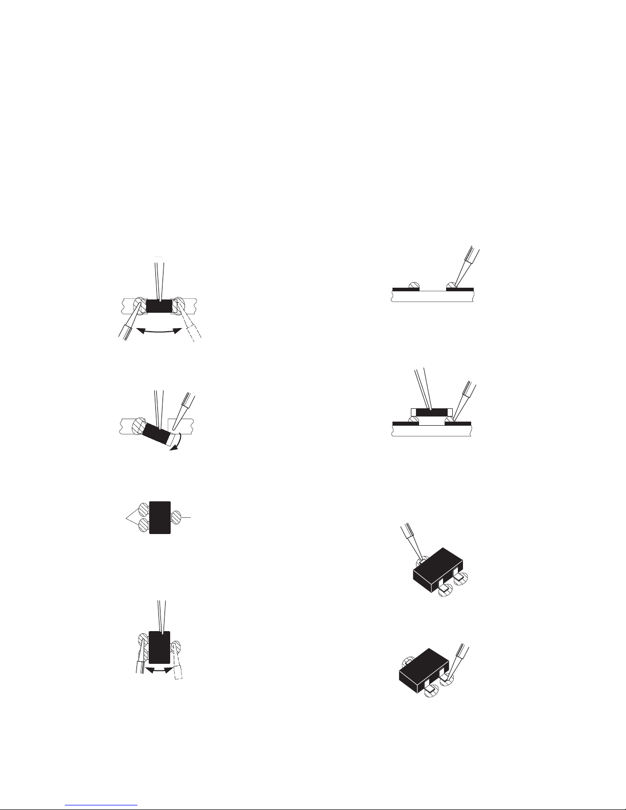
3.5 REPLACEMENT OF CHIP COMPONENT
3.5.1 CAUTIONS
(1) Avoid heating for more than 3 seconds.
(2) Do not rub the electrodes and the resist parts of the pattern.
(3) When removing a chip part, melt the solder adequately.
(4) Do not reuse a chip part after removing it.
3.5.2 SOLDERING IRON
(1) Use a high insulation soldering iron with a thin pointed end of it.
(2) A 30w soldering iron is recommended for easily removing parts.
3.5.3 REPLACEMENT STEPS
1. How to remove Chip parts
2. How to install Chip parts
[Resistors, capacitors, etc.]
(1) As shown in the figure, push the part with tweezers and
alternately melt the solder at each end.
(2) Shift with the tweezers and remove the chip part.
[Transistors, diodes, variable resistors, etc.]
(1) Apply extra solder to each lead.
SOLDER
SOLDER
[Resistors, capacitors, etc.]
(1) Apply solder to the pattern as indicated in the figure.
(2) Grasp the chip part with tweezers and place it on the
solder. Then heat and melt the solder at both ends of the
chip part.
[Transistors, diodes, variable resistors, etc.]
(1) Apply solder to the pattern as indicated in the figure.
(2) Grasp the chip part with tweezers and place it on the
solder.
(3) First solder lead A as indicated in the figure.
(2) As shown in the figure, push the part with tweezers and
alternately melt the solder at each lead. Shift and remove
the chip part.
NOTE :
After removing the part, remove remaining solder from the
pattern.
1-18 (No.YA408)
A
B
C
(4) Then solder leads B and C.
A
B
C
Page 19
SECTION 4
SERVICE MENU
1. ADJUST
2. SELF CHECK
3. I2C STOP
ADJUSTMENT
4.1 ADJUSTMENT PREPARATION
(1) There are 2 ways of adjusting this TV : One is with the
REMOTE CONTROL UNIT and the other is the
conventional method using adjustment parts and
components.
(2) The adjustment using the REMOTE CONTROL UNIT is
made on the basis of the initial setting values. The
setting values which adjust the screen to the optimum
condition can be different from the initial setting
values.
(3) Make sure that connection is correctly made AC to AC
power source.
(4) Turn on the power of the TV and measuring instruments for
warming up for at least 30 minutes before starting
adjustments.
(5) If the receive or input signal is not specified, use the most
appropriate signal for adjustment.
(6) Never touch the parts (such as variable resistors,
transformers and condensers) not shown in the adjustment
items of this service adjustment.
4.2 PRESET SETTING BEFORE ADJUSTMENTS
Unless otherwise specified in the adjustment items, preset the
following functions with the REMOTE CONTROL UNIT.
Setting item Settings position
Picture Mode Standard
Picture Adjustments Centre
Colour Temp. Normal
Super Digipure Auto
Movie Theatre Auto
Colour Management On
Picture Management On
Zoom Full
4.3 MEASURING INSTRUMENT AND FIXTURES
• Signal generator (Pattern generator) [PAL]
• Remote control unit
4.5 BASIC OPERATION OF SERVICE MODE
4.5.1 HOW TO ENTER THE SERVICE MODE
(1) Press [INFORMATION] key and [MUTING] key on the
remote control unit simultaneously to enter the SERVICE
MODE SCREEN.
(2) In the SERVICE MENU, press the [1] key to display
ADJUSTMENT MODE SCREEN.
SERVICE MENU SCREEN
SERVICE MENU
1. ADJUST
2. SELF CHECK
3. I2C STOP
NOTE:
• Before entering the SERVICE MODE, press the [MODE]
key to confirm that "TV" position is indicated. If it is in a
wrong position, the SERVICE MODE operation cannot be
performed.
• When a number key other than the [1] key is pressed in the
SERVICE MODE SCREEN, the other relevant screen may
be displayed.
This is not used in the adjustment procedure. Press the
[MENU] key to return to the SERVICE MODE SCREEN.
4.5.2 HOW TO EXIT THE SERVICE MODE
Press the [MENU] key to exit the Service mode.
4.5.3 SERVICE MODE SELECT KEY LOCATION
[MUTING] key
[Nunber] key
4.4 ADJUSTMENT ITEMS
VIDEO CIRCUIT
• WHITE BALANCE (HIGH LIGHT) adjustment
[INFORMATION] key
[Red] key
[MODE] key
[Function/] key
[Green] key
[MENU] key
[FUNCTION
/] key
(No.YA408)1-19
Page 20
4.5.4 ADJUSTMENT MODE
S001 R DRIVE 137
PAL50 FULL STD H
This mode is used to adjust the VIDEO CIRCUIT and the MTS CIRCUIT.
4.5.4.1 HOW TO ENTER THE ADJUSTMENT MODE
When the SERVICE MENU SCREEN of SERVICE MODE is displayed, press [1] key to enter the ADJUSTMENT MODE.
4.5.5 DESCRIPTION OF STATUS DISPLAY
(3) PICTURE MODE
SOFT : SOFT
ADJUSTMENT MODE
STD : STANDARD
BRI : BRIGHT
SETTING ITEM No.
SETTING ITEM
SETTING VALUE (DATA)
(4) COLOUR TEMP.
H: COOL
M : NORMAL
S001 R DRIVE 137
PAL50 FULL STD H
L: WARM
(5) SETTING ITEM NAME
Setting item name are displayed. For the setting item names
to be displayed, refer to "INITIAL SETTING VALUES IN THE
SERVICE MODE".
SIGNAL SYSTEM
ZOOM MODE
PICTURE MODE
COLOUR TEMP.
(1) SIGNAL SYSTEM
The signal displayed on the screen is displayed.
PAL50 : PAL50Hz (Composite / S-video)
PAL60 : PAL60Hz (Composite / S-video)
SECAM : SECAM
NTSC3 : NTSC3.58
NTSC4 : NTSC4.43
525I : 525i (Component)
525P : 525p
625I : 625i (Component)
625P : 625p
1125I5 : 1125i 50Hz
1125I6 : 1125i 60Hz
RGB5 : RGB 525i
RGB6 : RGB 625i
PCVGA : PC (VGA)
PCXGA : PC (XGA)
D625I : DVB-T 625i
H525I : HDMI 525i
H525P : HDMI 525p
H625I : HDMI 625i
H625P : HDMI 625p
H750P : HDMI 750p
H125I5 : HDMI 1125i 50Hz
H125I6 : HDMI 1125i 60Hz
--- : OTHER
(2) ZOOM MODE
State of the SCREEN SIZE or MULTI PICTURE is displayed.
SINGLE SCREEN
FULL : FULL
PANO : PANORAMIC
1609 : 16:9 ZOOM
1609S : 16:9 ZOOM SUBTITLE
1409 : 14:9 ZOOM
REGU : REGULAR
MULTI SCREEN
M2 : 2-pictures multi
M12 : 12-pictures multi
(6) SETTING ITEM NO.
Setting item numbers are displayed. The setting item numbers
to be displayed are listed below.
Item No. Setting item
S001 - S009 Video system setting
T001 - T003 Audio system setting
M001 - M224 Main CPU system setting
F001 - F002 Drive system setting
D001 (NOT USED)
Z001 (NOT USED)
(7) SETTING VALUE (DATA)
The SETTING VALUE is displayed.
4.5.6 CHANGE AND MEMORY OF SETTING VALUE
SELECTION OF SETTING ITEM
• [FUNCTION /] key.
For scrolling up / down the setting items.
S001...S009 ↔ T001...T003 ↔ M001...M224 ↔
F001...F002 ↔ D001 ↔ Z001↔return to S001
CHANGE OF SETTING VALUE (DATA)
• [FUNCTION /] key.
For scrolling up / down the setting values.
MEMORY OF SETTING VALUE (DATA)
Changed setting value is memorized by pressing [MUTING]
key.
1-20 (No.YA408)
Page 21
4.6 INITIAL SETTING VALUES IN THE SERVICE MODE
• Perform fine-tuning based on the "initial values" using the remote control when in the Service mode.
• The "initial values" serve only as an indication rough standard and therefore the values with which optimal display can be achieved
may be different from the default values. But, don't change the values that are not written in "ADJUSTMENT PROCEDURE". They
are fixed values.
4.6.1 VIDEO SYSTEM SETTING
Item No. Item Variable range Setting value
S001 R DRIVE 0 - 255 137
S002 G DRIVE 0 - 255 125
S003 B DRIVE 0 - 255 124
S004 RESREV 0 - 255 4
S005 RESREV 0 - 255 2
S006 RESREV 0 - 255 2
S007 RESREV 0 - 255 2
S008 RESREV 0 - 255 2
S009 RESREV 0 - 255 2
Item No. Item Variable range Setting value
M035 1E22 00 - FF 00
M036 1E23 00 - FF 00
M037 1E24 00 - FF 00
M038 1E25 00 - FF 00
M039 1E26 00 - FF 00
M040 1E27 00 - FF 00
M041 1E28 00 - FF 00
M042 1E29 00 - FF 00
M043 1E2A 00 - FF 00
M044 1E2B 00 - FF 00
M045 1E2C 00 - FF 00
4.6.2 AUDIO SYSTEM SETTING
Item No. Item Variable range Setting value
T001 RESREV 0 - 15 2
T002 RESREV 0 - 63 2
T003 RESREV 0 - 63 2
M046 1E2D 00 - FF 00
M047 1E2E 00 - FF 00
M048 1E2F 00 - FF 00
M049 1E30 00 - FF 00
M050 1E31 00 - FF 02
M051 1E32 00 - FF 01
4.6.3 MAIN CPU SYSTEM SETTING (Fixed values)
Item No. Item Variable range Setting value
M001 1E00 00 - FF 00
M002 1E01 00 - FF 00
M003 1E02 00 - FF 05
M004 1E03 00 - FF 01
M005 1E04 00 - FF 10
M006 1E05 00 - FF 00
M007 1E06 00 - FF 00
M008 1E07 00 - FF 16
M009 1E08 00 - FF 00
M010 1E09 00 - FF 00
M011 1E0A 00 - FF 01
M012 1E0B 00 - FF 00
M013 1E0C 00 - FF 01
M014 1E0D 00 - FF 00
M015 1E0E 00 - FF 00
M016 1E0F 00 - FF 00
M017 1E10 00 - FF 01
M018 1E11 00 - FF 00
M019 1E12 00 - FF 00
M020 1E13 00 - FF 01
M021 1E14 00 - FF 10
M022 1E15 00 - FF 01
M023 1E16 00 - FF 00
M024 1E17 00 - FF 00
M025 1E18 00 - FF 00
M026 1E19 00 - FF 00
M027 1E1A 00 - FF 00
M028 1E1B 00 - FF 00
M029 1E1C 00 - FF 00
M030 1E1D 00 - FF 00
M031 1E1E 00 - FF 00
M032 1E1F 00 - FF 00
M033 1E20 00 - FF 00
M034 1E21 00 - FF 00
M052 1E33 00 - FF 00
M053 1E34 00 - FF 00
M054 1E35 00 - FF 00
M055 1E36 00 - FF 01
M056 1E37 00 - FF 00
M057 1E38 00 - FF 05
M058 1E39 00 - FF 4E
M059 1E3A 00 - FF 00
M060 1E3B 00 - FF 30
M061 1E3C 00 - FF 00
M062 1E3D 00 - FF 00
M063 1E3E 00 - FF 00
M064 1E3F 00 - FF 00
M065 1E40 00 - FF 00
M066 1E41 00 - FF 00
M067 1E42 00 - FF 03
M068 1E43 00 - FF 30
M069 1E44 00 - FF 00
M070 1E45 00 - FF 20
M071 1E46 00 - FF 03
M072 1E47 00 - FF 00
M073 1E48 00 - FF 00
M074 1E49 00 - FF 00
M075 1E4A 00 - FF 03
M076 1E4B 00 - FF 03
M077 1E4C 00 - FF 03
M078 1E4D 00 - FF 01
M079 1E4E 00 - FF 03
M080 1E4F 00 - FF 00
M081 1E50 00 - FF 06
M082 1E51 00 - FF 00
M083 1E52 00 - FF 23
M084 1E53 00 - FF 00
M085 1E54 00 - FF 00
M086 1E55 00 - FF 00
M087 1E56 00 - FF 00
(No.YA408)1-21
Page 22

Item No. Item Variable range Setting value
M088 1E57 00 - FF 00
M089 1E58 00 - FF 00
M090 1E59 00 - FF 00
M091 1E5A 00 - FF 00
M092 1E5B 00 - FF 00
M093 1E5C 00 - FF 00
M094 1E5D 00 - FF 00
M095 1E5E 00 - FF 00
M096 1E5F 00 - FF 00
M097 1E60 00 - FF 00
M098 1E61 00 - FF 00
M099 1E62 00 - FF 00
M100 1E63 00 - FF 00
M101 1E64 00 - FF 00
M102 1E65 00 - FF 00
M103 1E66 00 - FF 00
M104 1E67 00 - FF 00
M105 1E68 00 - FF 00
M106 1E69 00 - FF 00
M107 1E6A 00 - FF 02
M108 1E6B 00 - FF 00
M109 1E6C 00 - FF 00
M110 1E6D 00 - FF 00
M111 1E6E 00 - FF 00
M112 1E6F 00 - FF 00
M113 1E70 00 - FF 00
M114 1E71 00 - FF 00
M115 1E72 00 - FF 00
M116 1E73 00 - FF 00
M117 1E74 00 - FF 00
M118 1E75 00 - FF 00
M119 1E76 00 - FF 00
M120 1E77 00 - FF 0F
M121 1E78 00 - FF 00
M122 1E79 00 - FF 00
M123 1E7A 00 - FF 00
M124 1E7B 00 - FF 00
M125 1E7C 00 - FF 00
M126 1E7D 00 - FF 00
M127 1E7E 00 - FF 02
M128 1E7F 00 - FF 00
M129 1E80 00 - FF 01
M130 1E81 00 - FF 00
M131 1E82 00 - FF 01
M132 1E83 00 - FF 00
M133 1E84 00 - FF 00
M134 1E85 00 - FF 00
M135 1E86 00 - FF 00
M136 1E87 00 - FF 00
M137 1E88 00 - FF 00
M138 1E89 00 - FF 00
M139 1E8A 00 - FF 00
M140 1E8B 00 - FF 00
M141 1E8C 00 - FF 00
M142 1E8D 00 - FF 00
M143 1E8E 00 - FF 00
M144 1E8F 00 - FF 00
M145 1E90 00 - FF 00
Item No. Item Variable range Setting value
M146 1E91 00 - FF 00
M147 1E92 00 - FF 00
M148 1E93 00 - FF 00
M149 1E94 00 - FF 00
M150 1E95 00 - FF 00
M151 1E96 00 - FF 00
M152 1E97 00 - FF 00
M153 1E98 00 - FF 00
M154 1E99 00 - FF 00
M155 1E9A 00 - FF 01
M156 1E9B 00 - FF 00
M157 1E9C 00 - FF 03
M158 1E9D 00 - FF 00
M159 1E9E 00 - FF 00
M160 1E9F 00 - FF 00
M161 1EA0 00 - FF 00
M162 1EA1 00 - FF 00
M163 1EA2 00 - FF 01
M164 1EA3 00 - FF 00
M165 1EA4 00 - FF 00
M166 1EA5 00 - FF 00
M167 1EA6 00 - FF 00
M168 1EA7 00 - FF 00
M169 1EA8 00 - FF 00
M170 1EA9 00 - FF 00
M171 1EAA 00 - FF 00
M172 1EAB 00 - FF 00
M173 1EAC 00 - FF 0A
M174 1EAD 00 - FF 00
M175 1EAE 00 - FF 00
M176 1EAF 00 - FF 00
M177 1EB0 00 - FF 00
M178 1EB1 00 - FF 00
M179 1EB2 00 - FF 00
M180 1EB3 00 - FF 00
M181 1EB4 00 - FF 00
M182 1EB5 00 - FF 00
M183 1EB6 00 - FF 00
M184 1EB7 00 - FF 00
M185 1EB8 00 - FF 00
M186 1EB9 00 - FF 00
M187 1EBA 00 - FF 00
M188 1EBB 00 - FF 00
M189 1EBC 00 - FF 00
M190 1EBD 00 - FF 00
M191 1EBE 00 - FF 00
M192 1EBF 00 - FF 00
M193 1EC0 00 - FF 00
M194 1EC1 00 - FF 00
M195 1EC2 00 - FF 01
M196 1EC3 00 - FF 00
M197 1EC4 00 - FF 00
M198 1EC5 00 - FF 00
M199 1EC6 00 - FF 00
M200 1EC7 00 - FF 00
M201 1EC8 00 - FF 01
M202 1EC9 00 - FF 00
M203 1ECA 00 - FF 00
1-22 (No.YA408)
Page 23
Item No. Item Variable range Setting value
M204 1ECB 00 - FF 00
M205 1ECC 00 - FF 02
M206 1ECD 00 - FF 00
M207 1ECE 00 - FF 00
M208 1ECF 00 - FF 00
M209 1ED0 00 - FF 10
M210 1ED1 00 - FF 00
M211 1ED2 00 - FF 00
M212 1ED3 00 - FF 00
M213 1ED4 00 - FF 00
M214 1ED5 00 - FF FF
M215 1ED6 00 - FF 00
M216 1ED7 00 - FF 00
M217 1ED8 00 - FF 00
M218 1ED9 00 - FF 00
M219 1EDA 00 - FF 00
M220 1EDB 00 - FF 00
4.7 ADJUSTMENT PROCEDURE
4.7.1 VIDEO CIRCUIT
Item
WHITE
BALANCE
(HIGHLIGHT)
Measuring
instrument
Remote
control unit
Signal
Test point Adjustment part Description
[1.ADJUST]
S001: R DRIVE (Red drive)
S002: G DRIVE (Green drive)
S003: B DRIVE (Blue drive)
generator
Item No. Item Variable range Setting value
M221 1EDC 00 - FF 00
M222 1EDD 00 - FF 00
M223 1EDE 00 - FF 00
M224 1EDF 00 - FF 00
4.6.4 DRIVE SYSTEM SETTING (Fixed values)
Item No. Item Variable range Setting value
F001 DD 0 - 1 0
F002 RAM REF 0 - 1 0
4.6.5 NOT USED (Fixed values)
Item No. Item Variable range Setting value
D001 RESREV 0 - 255 2
4.6.6 NOT USED (Fixed values)
Item No. Item Variable range Setting value
Z001 RESREV 0 - 255 2
(1) Receive a PAL 75% all white signal.
(2) Set PICTURE MODE to "STANDARD".
(3) Set ZOOM to "FULL".
(4) Set COLOUR TEMP. to "NORMAL".
(5) Select "1.ADJUST" from the SERVICE MODE.
(6) Adjust to Keep one of < S001 > (Red drive),
< S002 > (Green drive) or < S003 > (Blue drive)
unchanged, then lower the other two so that the
all-white screen is equally white throughout.
NOTE:
Set one or more of < S001 >, < S002 >, and
< S003 > to "137".
(7) Check that white balance is properly tracked
from low light to high light. If the white balance
tracking is deviated, adjust to correct it.
(8) Press the [MUTING] key to memoirze the set
value.
(No.YA408)1-23
Page 24
SECTION 5
SERVICE MENU
1. ADJUST
2. SELF CHECK
3. I2C STOP
LOB 0 FAN 0
AUD 0
ANA 9 DIG 9
0000 00
00
TMP 0 L 1 0
L 2 0 DDT 0
FAN 0 L C 0
IRS 0
TROUBLESHOOTING
5.1 SELF CHECK FEATURE
5.1.1 OUTLINE
This unit comes with the "Self check" feature, which checks the
operational state of the circuit and displays/saves it during
failure.Diagnosis is performed when power is turned on, and
information input to the main microcomputer is monitored at all
time.Diagnosis is displayed in 2 ways via screen display and LED
flashes. Failure detection is based on input state of I
2
C bus and
the various control lines connected to the main microcomputer.
5.1.2 HOW TO ENTER THE SELF CHECK MODE
Before enter the SELF CHECK MODE, press the [MODE] key to
confirm that "TV" position is indicated. If it is in a wrong position,
the SELF CHECK MODE operation cannot be performed.
(1) Press the [INFORMATION] key and [MUTING] key
simultaneously, then enter the SERVICE MODE.
(2) Press the [2] key SELF CHECK MODE.
(3) Press the [RED] key to enter Page 2 of the SELF CHECK
MODE.
*Use the [GREEN] key to toggle between Page 1 and Page 2.
NOTE:
When a number key other than the [2] key is pressed in the
SERVICE MODE screen, the other relevant screen may be
displayed.
This is not used in the SELF CHECK MODE. Press the
[MENU] key to return to the MAIN MENU SCREEN.
5.1.3 HOW TO EXIT THE SELF CHECK MODE
To Save Failure History:
Turn off the power by unplugging the AC power cord plug when
in the Self check display mode.
To Clear (Reset) Failure History:
Turn off the power by pressing the [POWER] key on the remote
control unit when in the Self check display mode.
5.1.4 FAILURE HISTORY
Failure history can be counted up to 9 times for each item. When
the number exceeds 9, display will remain as 9. Failure history
will be stored in the memory unless it has been deleted.
NOTE:
Only SYNC (with/without sync signals) will be neither counted
nor stored.
5.1.5 POINTS TO NOTE WHEN USING THE SELF CHECK
FEATURE
In addition to circuit failures (abnormal operation), the following
cases may also be iagnosed as "Abnormal" and displayed and
counted as "NG".
(1) Temporary defective transmissions across circuits due to
pulse interruptions
(2) Misalignment in the on/off timing of power for I
2
C bus
(VCC) when turning on/off the main power.
Diagnosis may be impeded if a large number of items are
displayed as "NG". As such, start Self check check only after 3
seconds in the case of receivers and 5 seconds in the case of
panels upon turning on the power. If recurrences are expected,
ensure to clear (reset) the failure history and record the new
diagnosis reults.
SERVICE MENU SCREEN
SERVICE MENU
1. ADJUST
2. SELF CHECK
3. I2C STOP
SELF CHECK MODE SCREEN (Page 1)
LOB 0 FAN 0
AUD 0
ANA 9 DIG 9
0000 00
00
Item Failure history
1-24 (No.YA408)
SELF CHECK MODE SCREEN (Page 2)
TMP 0 L 1 0
L 2 0 DDT 0
FAN 0 L C 0
IRS 0
Item Failure history
Fig.1
Page 25
5.1.6 DETAILS
Self check is performed for the following items:
< Page 1 of screen >
Detection item Display Detection content
Low bias line short
protection
LOB Confirm the operation of the low bias (16V / 5V /
LCD5V / 3.3V / 1.2V) protection circuit.
, Q9651[DC-DC PWB]
Q9601
Diagnosis
signal (line)
Detection timing
LB_PRO Detection starts 3 seconds after
the power is turned on. If error
continues between 200 ms the
power is turned off.
Fan lock FAN Not used ---- ----
Abnormal rise of
temperature in audio
circuit
AUD Confirmation of the temperature of audio circuit.
TH6401
[D-AMP PWB]
---- Detection starts 3 seconds after
the power is turned on.
If the temperture of 90°C is
detected for 3 seconds the power
is turned off.
Devices on the ANALOG
PWB
Devices on the DIGITAL
PWB
ANA Confirmation of reply of ACK signal which uses
I2C communication.
, IC102, IC381, IC601, IC606, TU3002
IC101
[ANALOG PWB]
DIG Confirmation of reply of ACK signal which uses
I2C communication.
[DIGITAL PWB]
IC6401
SDA If it checks whenever I2C
communication is performed and
no reply of ACK signal an error
will be counted.
SDA If it checks whenever I2C
communication is performed and
no reply of ACK signal an error
will be counted.
< Page 2 of screen >
Detection item Display Detection content
Diagnosis
signal (line)
Detection timing
Temp. sensor TEM Not used ---- ----
Lamp does not light up L1 Not used ---- ----
Lamp goes out L2 Not used ---- ----
Abnormal DD CPU
DDT Not used ---- ----
circuit
Fan lock FAN Not used ---- ----
Lamp cover open LC Not used ---- ----
Abnormal of optical iris IRS Not used ---- ----
5.1.7 METHOD OF DISPLAY WHEN A RASTER IS NOT OUTPUT
In the state where a raster is not output by breakdown of the set, an error is displayed by blink of the POWER LED.
Type of error POWER LED flash cycle
Low bias line short protection Red turnig on and off at 1 second intervals.
Abnormal rise of temperature in audio circuit Green turnig on and off at 0.5 second intervals.
< Explanation of operation >
If error is detected, the power is turned off.
Shortly after a power is turned off, POWER LED will be blinked.
Power cannot be turned on until the power cord takes out and inserts, after a power is turned off.
(No.YA408)1-25
Page 26

Victor Company of Japan, Limited
Flat Panel Display Category 12, 3-chome, Moriya-cho, Kanagawa-ku, Yokohama-city, Kanagawa-prefecture, 221-8528, Japan
(No.YA408)
Printed in Japan
VPT
Page 27
© 2006 Victor Company of Japan, Limited 0306KTH-SW-MU LCT2090-001A-U
If you have any problems setting up your
new TV, please call the
Helpline on
If you have any problems setting up your
new TV, please call the
Helpline on
For users in the UK :
0870 330 5000.
1890-582500.
For users in the Republic of Ireland :
WIDE LCD PANEL TV INSTRUCTIONS
Trade Mark of the DVB Digital Video Broadcasting
Project (1991 to 1996) Number : 3988, 3989, 3990, 3991, 3992, 3993
LT-37DR7BJ LT-37DR7SJ
LT-32DR7BJ LT-32DR7SJ
LT-26DR7BJ LT-26DR7SJ
1-2 3/6/2006 1:24:22 PM
Page 28
1
Information for Users on Disposal of Old Equipment
ENGLISH
[European Union]
This symbol indicates that the electrical and electronic equipment should not be disposed as
general household waste at its end-of-life. Instead, the product should be handed over to the
applicable collection point for the recycling of electrical and electronic equipment for proper
treatment, recovery and recycling in accordance with your national legislation.
By disposing of this product correctly, you will help to conserve natural resources and will
help prevent potential negative effects on the environment and human health which could
otherwise be caused by inappropriate waste handling of this product. For more information
about collection point and recycling of this product, please contact your local municipal
office, your household waste disposal service or the shop where you purchased the product.
Penalties may be applicable for incorrect disposal of this waste, in accordance with national
legislation.
(Business users)
If you wish to dispose of this product, please visit our web page www.jvc-europe.com to
obtain information about the take-back of the product.
[Other Countries outside the European Union]
If you wish to dispose of this product, please do so in accordance with applicable national
legislation or other rules in your country for the treatment of old electrical and electronic
equipment.
Attention:
This symbol is only
valid in the European
Union.
2-1 3/6/2006 1:24:22 PM
Page 29
2
3
IMPORTANT! PREPARE USE
SETTINGS
TROUBLE?
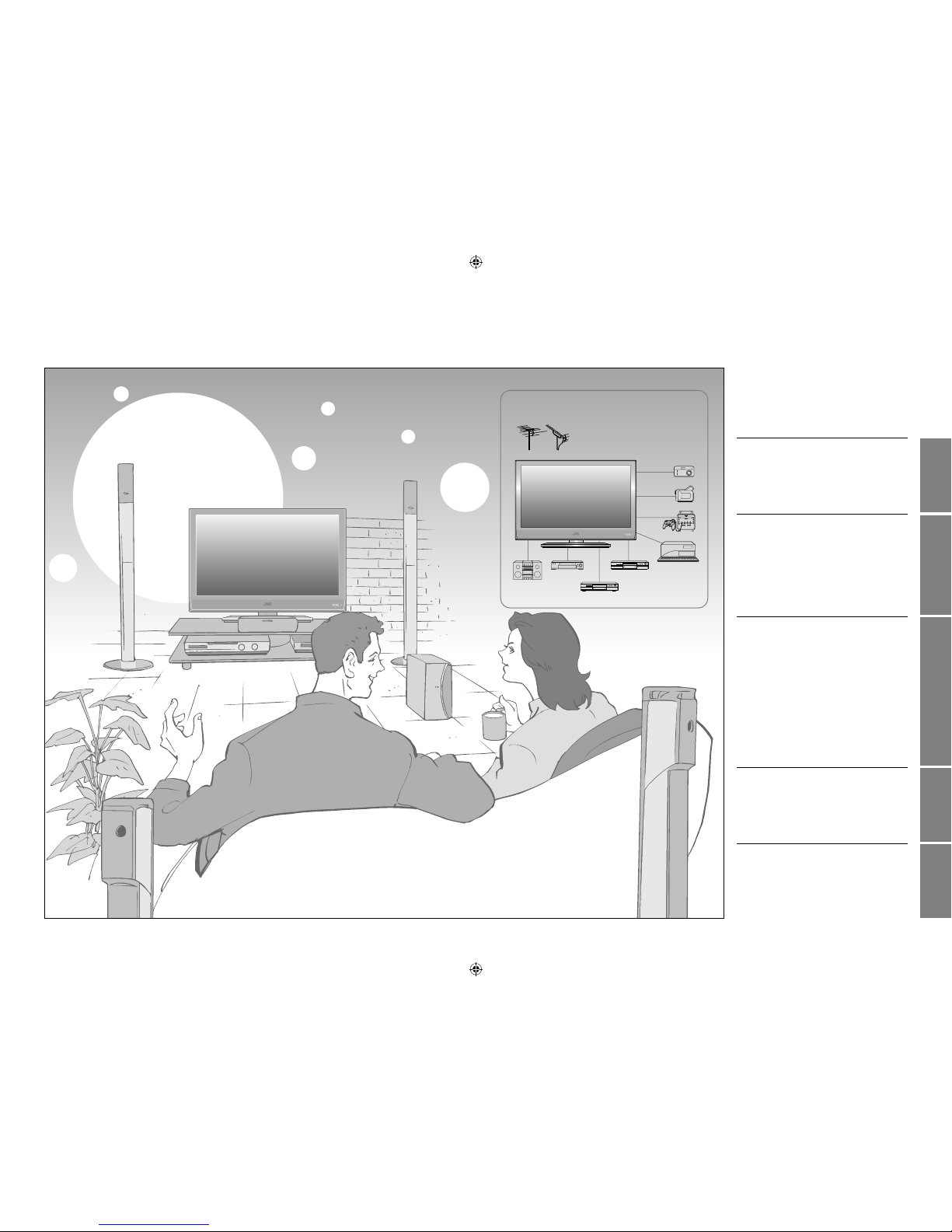
Expanding the world of
Enjoy rich multi-media with JVC
VHF / UHF / DVB-T broadcasting
Digital camera
Video camera
Game console
Audio components
VCR DVD player
DVD recorder
Personal
computer
beautiful images
First things first!
Warning ············································4
Getting started
Names of all the parts ······················6
Basic connections ····························8
Connecting external devices ·········· 10
Initial settings ································· 12
Editing DTV channels ····················· 14
Editing ATV channels ····················· 16
Let’s try it out
Enjoying your new TV! ···················18
· TV / Teletext / EPG / Video / Menu
Watching TV ··································· 20
Using EPG ····································· 22
Viewing teletext ······························ 24
Watching videos / DVDs ················ 26
Try the advanced features
Useful functions ······························ 28
· Multi-picture / Favourite channel
· Sleep timer / Child lock
Useful functions ······························ 30
Operate JVC recorders and other devices
··· 32
Just the way you like it
Customising your TV ······················ 34
Using DTV ······································ 36
Advanced picture adjustment ········· 42
· Reduce noise / Watch a more natural picture
· Set the aspect ratio, etc.
When you have trouble
Troubleshooting ····························· 44
CH/CC List ·····································47
Technical information ····················· 48
Specifications ································· 49
Contents
* In this manual,
ATV : analogue terrestrial broadcasting (VHF / UHF)
DTV : digital terrestrial broadcasting (DVB-T)
Contents_EN.indd 2-3 3/6/2006 2:21:16 PM
Page 30
4
5
First things first!
IMPORTANT! PREPARE USE
SETTINGS
TROUBLE?
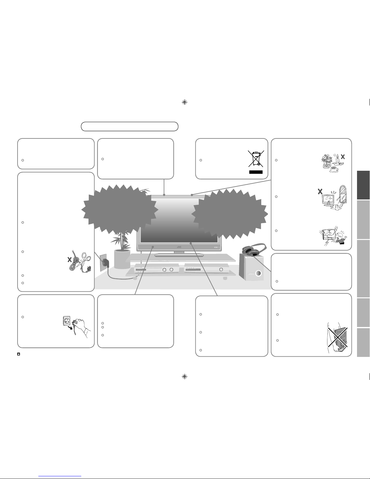
Never dismantle the
rear panel!
It may cause an electric shock.
Never obstruct the
ventilation holes!
It may cause overheating or a fire.
Handle LCD panel
with care!
Use a soft, dry cloth when cleaning.
Never try to repair
the TV yourself!
If the problem cannot be solved in
“Troubleshooting” (P. 44), unplug
the power cord and contact your
retailer.
If the TV is damaged
or behaving strangely,
stop using it at once!
Unplug the power cord and contact
your retailer.
Warning
For more details on installation, usage and safety
Consult your retailer
Never expose to rain or
moisture!
To prevent fire or electric
shock, never allow
liquids to enter the unit.
Hold the TV so as not to
scratch the screen!
Do not touch the screen when carrying the
TV.
Do not carry the
TV on your own!
In order to prevent accidents,
ensure that the TV is carried
by two or more people.
Please follow all the guidelines below
Never listen to
headphones at high
volume!
It may damage your hearing.
Never place anything on
the TV!
Placing liquids, naked
flames, cloths, paper,
etc. on the TV may
cause a fire.
Never insert objects into
the cabinet openings!
It may cause a fatal
electric shock. Take care
when children are near.
Unplug the power cord
when going out!
The power buttons on
the remote control and
the TV unit cannot
completely turn off the
TV. (Make appropriate
arrangements for
bedridden people.)
For more details on installation, usage and safety
Consult your retailer
Make enough room for
inserting and removing
the power plug!
Place the TV as
close to the outlet as
possible!
The main power supply for this TV is
controlled by inserting or removing the
power plug.
Never cut or damage
the power cord!
If the AC plug is not the
right shape, or the power
cord is not long enough,
use an appropriate plug
adapter or extension cable.
(Consult your retailer.)
If you have cut or damaged the power cord.
“Technical information” (P. 48)
To change the fuse in UK plugs
“Technical information” (P. 48)
Follow this manual
regarding setup!
Connect only to a 220-240V, 50Hz AC
outlet.
On disposal of the
TV!
Follow the instruction in
“Information for Users on
Disposal of Old Equipment”
(P. 1).
When attaching the TV to
the wall, use the optional
JVC wall mounting unit!
Consult a qualified technician.
See the included manual on mounting
procedures.
JVC assumes no responsibility for
damage due to improper mounting.
Do not allow the TV
to fall!
Do not rest your elbows on, or allow
children to hang from the TV.
There is a risk that the TV will fall and
cause injuries.
4-5 3/6/2006 1:24:26 PM
Page 31

6
7
Getting
started
TV/AV
MENU
/OK
P
IMPORTANT! PREPARE USE
SETTINGS
TROUBLE?
Turn on “3D Cinema Sound” (P. 20)
Take a snapshot
of the screen
(P. 20)
View in multi-picture mode
(P. 28)
When watching TV / Video
Change the aspect ratio
(P. 20)
When operating a JVC VCR
or DVD
(P. 26)
When choosing a favourite
channel
(P. 29)
View subtitles
(P. 20)
View the electronic
programme guide (EPG)
(P. 22
)
When watching DTV
when viewing teletext
(P. 24)
When watching ATV
(P. 16)
Names of all the parts
Remote control sensorPower lamp
ON: Lit (Green)
OFF: Unlit
Power lamp lights while
the TV is on.
“Power Lamp” (P. 35)
If the cover cannot be closed due to the cables being in the way
Do not force the cover to close (leave it open).
Connecting terminals on the back of the TV Connecting External devices
(P. 10)
To remove the cable cover, refer to the included sheet.
LT-26DR7BJ/SJ
Remove the terminal cover
Direction of TV
Remote control
(RM-C1905S)
Check accessories
To ATV / DTV
Power On / Off
Change channel / page
Watch video, etc.
(P. 26)
Select and
confirm settings in menus
To previous channel
Change channel / page
Switch between
“TV / VCR / DVR / DVD / HC”
(P. 21)
Mute
Channel information
(P. 20)
Display on-screen menu
(P. 34)
Colour buttons
Volume
To teletext
(P. 24)
AAA/R03 Batteries
For confirming
the TV works
Insert the batteries
Use two “AAA/R03” dry cell batteries. Insert the batteries from
the - end, making sure the + and - polarities are correct.
Tidying the cables
To remove the cable cover,
refer to the included sheet.
Change channel / page
Volume
Power On / Off
To headphones
(P. 10)
Display on-screen
menu / set
Switch between
TV / AV devices
LT-26DR7BJ/SJ
To attach the stand, refer to the included sheet.
LT-32DR7BJ/SJ
LT37DR7BJ/SJ LT32DR7BJ/SJ, LT26DR7BJ/SJ
LT-37DR7BJ/SJ
Press to
remove.
Press to
remove.
Press to
remove.
Cable cover
LT37DR7BJ/SJ
For LT-32DR7BJ/SJ and
LT-26DR7BJ/SJ, the
direction of the TV is fixed.
Cable cover
6-7 3/6/2006 1:24:41 PM
Page 32

8
9
CAM
IMPORTANT! PREPARE USE
SETTINGS
TROUBLE?
Basic connections
200mm
50mm150mm 150mm 50mm
Power requirements
Connect the power cord only to a 220-240V, 50Hz
AC outlet.
When attaching the TV to the wall, use the
optional JVC wall mounting unit
Consult a qualified technician.
See the included manual on mounting procedures.
JVC assumes no responsibility for damage due to
improper mounting.
200mm × 200mm mount which conforms to VESA
standards.
Installation requirements
To avoid overheating, ensure the unit has ample
room.
Please read the user manuals of each device carefully before setup.
It is necessary to connect an aerial to watch TV.
Connect with other devices “Connecting external devices” (P. 10)
Care when setting Watch pay-per-view
Contract with a broadcasting company beforehand.
1 Unplug the power cord
2 Insert the Viewing Card into the CAM.
3 Insert the CAM.
4 Plug the power cord, and turn the power on.
Set pay-per-view (P. 40)
The CAM and Viewing Card will be sent by the broadcasting
company after contracting with them.
Connect the aerial
After all the connections have been made, insert the plug into an AC outlet.
AERIAL
VCR / DVD recorder
After all the connections have been made, insert the plug into an AC outlet.
Connect “T-V LINK” compatible recording device to “EXT-2”.
“T-V LINK” “What is “T-V LINK”?” (P. 12)
EXT-2
Connect a VCR / DVD recorder
AERIAL
EXT-1
Viewing
Card
Conditional
Access
Module
8-9 3/6/2006 1:24:53 PM
Page 33

10
11
IMPORTANT! PREPARE USE
SETTINGS
TROUBLE?
Connecting external devices
You can connect many different devices to the rear panel of the TV.
Please read the user manuals of each device before setting up.
(Connecting cables are not supplied with this TV.)
: signal direction
Connect “DVI” devices
(P. 48)
“T-V LINK” (P. 12)
EXT-1
Watching videos
Output Input
· Composite signal
· Sound L / R
·
Composite signal /
RGB / S-VIDEO
· Sound L / R
Use S-VIDEO “S-IN” (P. 27)
EXT-2
Dubbing videos
Using “T-V LINK”
Output Input
· Composite signal
· S-VIDEO (only for
DTV)
· Sound L / R
·
Composite signal /
RGB / S-VIDEO
· Sound L / R
· T-V LINK
Use S-VIDEO “S-IN” (P. 27)
Use DTV S-OUT “S-OUT” (P. 27)
Select dubbing sources
“DUBBING” (P. 27)
Connect a decoder
“Decoder (EXT-2)” (P. 35)
EXT-3
Watching videos
Output Input
· Composite
signal / S-VIDEO
· Sound L / R
EXT-4
Watching DVDs
Output Input
·
Component signal
(P. 49)
· Sound L / R
“Component Auto Select” (P. 35)
EXT-5
Connecting
HDMI devices
Output Input
· HDMI signal
(P. 49)
“HDMI Setting” (P. 35)
AUDIO OUT
Listening to the TV on external speakers
Output
· Sound L / R
VCR / DVD / other devices
AERIAL
DVD player
(HDMI compatible)
Amplifier
(L) (R)
VCR / DVD recorder
(“T-V LINK” compatible)
AUDIO
OUT
Satellite broadcast tuner
Game consoles
Check for PC compatibility
“Technical information” (P. 48)
DVD player
PC IN
PC
Video camera
EXT-1
EXT-2
(T-V LINK)
EXT-3
EXT-4
To “EXT-3” R/L (PC IN)
Headphones
(R)
Headphone
(L)
(Y)
(Pb)
(Pr)
(R)
(R)
(L)
(L)
EXT-5
(HDMI)
Not available.
(For service adjustments)
CAM slot
(“Watch pay-per-view” P.9)
Audio signals received from
EXT-5 cannot be sent to
the “AUDIO OUT” terminal.
10-11 3/6/2006 1:24:55 PM
Page 34

12
13
Installation > Automatic Search
Channels:
100%
BBC ONE
BBC TWO
BBC THREE
BBC NEWS 24
BBCi
CBBC Channel
UHF CH:68
1 BBC ONE
Select Delete Edit Name Lock Favourites
EDIT PR LIST
1. BBC ONE
2. BBC TWO
7. BBC THREE
30. CBBC Channel
40. BBC NEWS 24
51. BBCi
CH 28
>> Auto Program
14%
> Auto Program
United Kingdom
Country
Ireland
01
AV
PR
02
03
04
05
06
07
08
09
ID CH/CC
BBC1 CH
21
CH
22
CH
23
CH
24
CH
25
CC
02
CC
CC
04
CC
05
03
>Edit
Download TV Recording Device
T-V LINK
IMPORTANT! PREPARE USE
SETTINGS
TROUBLE?
Initial settings
Register DTV / ATV channels on TV. These channels can be edited later.
(In this manual, digital broadcasting is indicated as DTV, and analogue broadcasting as ATV.)
Begin
Automatically register DTV channels
Check what was registered
Automatically register ATV channels
Check what was registered
select
Edit ATV channels
@ in “Editing ATV
channels” (P. 16)
When not using T-V LINK
When using T-V LINK
If “Feature Not
Available” appears :
Is a T-V LINK compatible
device connected to EXT-2?
Is the device turned on?
If “ACI Start” appears, select and start settings.
(This will set up cable television channels.)
“What is ACI (Automatic Channel
Installation)?” (P. 48)
Finish
4
Confirm
Edit DTV channels
@ in “Editing DTV
channels” (P. 14)
Confirm
To the previous screen
Exit
MENU
BACK
What is “T-V LINK”?
Connecting the TV to a “T-V LINK”
compatible device allows :
ATV channels on the TV to be
instantly registered on the device.
The “DIRECT REC” function to be
used.
“Technical information”
(P. 48)
“T-V LINK” variations
“T-V LINK” (JVC) “Q-LINK” (Panasonic)
“Megalogic” (Grundig) “Data Logic” (Metz)
“SMARTLINK” (Sony) “Easy Link” (Philips)
TV/DTV
If the “JVC” logo does not appear or
if you wish to make changes later
DTV : “Automatic Search” (P. 40)
ATV : “Auto Program” (P. 35)
The remote control
doesn’t work
Confirm the mode is set to
“TV”.
Shown only when powering on for the first time.
The power on the unit can also be used.
3
2
1
5
6
12-13 3/6/2006 1:25:20 PM
Page 35

14
15
1 BBC ONE
Edit Name Lock Favourites
EDIT PR LIST
1. BBC ONE
2. BBC TWO
7. BBC THREE
30. CBBC Channel
40. BBC NEWS 24
51. BBCi
DeleteSelect
DTV
Timers
Configuration
Installation
Common Interface
DTV
Edit PR List
1 BBC ONE
Select Delete Edit Name Lock Favourites
EDIT PR LIST
1. BBC ONE
2. BBC TWO
7. BBC THREE
30. CBBC Channel
40. BBC NEWS 24
51. BBCi
Red: Page up
Green: Pagedown
TV/DTV: Go to DTV
Guide: Go to guide
Back: Go to previous
i: Exit help
MENU
OK
7 BBC THREE
Edit Name Lock Favourites
EDIT PR LIST
1. BBC ONE
2. BBC TWO
7. BBC THREE
30. CBBC Channel
40. BBC NEWS 24
51. BBCi
DeleteSelect
1 BBC ONE
Select Edit Name Lock Favourites
EDIT PR LIST
1. BBC ONE
2. BBC TWO
7. BBC THREE
30. CBBC Channel
40. BBC NEWS 24
51. BBCi
Delete
1. BBC ONE
2. BBC TWO
7. BBC THREE
30. CBBC Channel
40. BBC NEWS 24
51. BBCi
1 BBC ONE
Select Delete Edit Name Lock Favourites
EDIT PR LIST
The selected service will be permanently
deleted. Are you sure?
NoYes
1 BBC ONE
Select Edit Name Lock Favourites
EDIT PR LIST
1. BBC ONE
2. BBC TWO
7. BBC THREE
40. BBC NEWS 24
51. BBCi
Delete
30. CBBC Channel
1 BBC ONE
Select Delete Lock Favourites
EDIT PR LIST
1. BBC ONE
2. BBC TWO
30. CBBC Channel
40. BBC NEWS 24
51. BBCi
7. BBC THREE
Edit Name
1 BBC ONE
1. BBC ONE
2. BBC TWO
7. BBC THREE
30. CBBC Channel
40. BBC NEWS 24
51. BBCil
EDIT PR LIST
Enter PIN code
1 BBC ONE
Select Delete Edit Name Lock Favourites
1. BBC ONE
2. BBC TWO
7. BBC THREE
30. CBBC Channel
40. BBC NEWS 24
51. BBCi
EDIT PR LIST
BBC 3CH
1 BBC ONE
Select Delete Lock Favourites
EDIT PR LIST
1. BBC ONE
2. BBC TWO
30. CBBC Channel
40. BBC NEWS 24
51. BBCi
Edit Name
7. BBC 3CH
1 BBC ONE
Select Delete Favourites
EDIT PR LIST
1. BBC ONE
2. BBC TWO
30. CBBC Channel
40. BBC NEWS 24
51. BBCi
7. BBC THREE
Edit Name Lock
1 BBC ONE
Select Delete Edit Name Lock Favourites
1. BBC ONE
2. BBC TWO
7. BBC THREE
30. CBBC Channel
40. BBC NEWS 24
51. BBCi
EDIT PR LIST
BBC
1 BBC ONE
EDIT PR LIST
1. BBC ONE
2. BBC TWO
30. CBBC Channel
40. BBC NEWS 24
51. BBCi
7. BBC THREE
1 BBC ONE
Select Delete Lock
EDIT PR LIST
1. BBC ONE
2. BBC TWO
30. CBBC Channel
40. BBC NEWS 24
51. BBCi
7. BBC THREE
Edit Name Favourites
1 BBC ONE
EDIT PR LIST
1. BBC ONE
2. BBC TWO
30. CBBC Channel
40. BBC NEWS 24
51. BBCi
7. BBC THREE
IMPORTANT! PREPARE USE
SETTINGS
TROUBLE?
When coming from “Initial settings” (P. 12), skip to @.
Editing DTV channels
Edit the channels registered with “Automatic search” in “Initial settings” (P. 12).
To the previous
screen
Exit
1
2
3
4
5
6
7
select
Display the menu bar
Select “DTV”
Select “Edit PR List”
Select a channel
Select DTV
Finish
Edit
Tips for operation
Confirm
the channel
picture
Select
Edit a
channel name
Edit Name
1 Select “Select”
2 Select “Yes”
3 Decide
1 Select “Delete”
2 Change the name1 Select “Edit Name”
2 Enter PIN code1 Select “Lock”
1 Select “Favourites”
Lock icon
Favourite icon
Delete
a channel
Delete
Stop Children
from watching
specific
channels
Lock
Register your
favourite
channel
Favourites
1 select
2 next
1 select
2 delete
1 select
2 next
1 enter character
2 move position
1 select
2 next
1 select
2 set
Default is “0000”.
“Change the PIN code” (P. 39)
To release, repeat the
same steps.
To release, repeat the
same steps.
Move through only your
favourite channels
“Favourite Mode” (P. 39)
1 select
2 view
1 select
2 next
1 select
2 next
14-15 3/6/2006 1:28:30 PM
Page 36

16
17
Download TV Recording Device
T-V LINK
Set Up
Set Up
Auto Program
Component Auto Select
EXT Setting
Off
Off
Off
HDMI Setting
Edit/Manual
Decoder(EXT-2)
Attenuator
PC Position
Set Up
Auto Program
Component Auto Select
EXT Setting
Off
Off
Off
HDMI Setting
Edit/Manual
Decoder(EXT-2)
Attenuator
PC Position
01
AV
PR
02
03
04
05
06
07
08
09
ID CH/CC
BBC1 CH
21
CH
22
CH
23
CH
24
CH
25
CC
02
CC
CC
04
CC
05
03
>Edit
ID
>Manual
11
10
PR
12
13
14
15
16
17
CH
CH
35
CH
29
01
AV
PR
02
03
04
05
06
07
08
09
CH
BBC1 CH
21
BBC2 CH
22
ITV CH
23
CH4 CH
24
CH5 CH
25
CH
26
CH
27
CH
28
>Edit
ID
01
AV
PR
02
03
04
05
06
07
08
09
ID CH
BBC1 CH
21
BBC2 CH
22
ITV CH
23
CH4 CH
24
CH5 CH
25
CH
26
CH
27
CH
28
>Edit
01
AV
PR
02
03
04
05
06
07
08
09
ID CH
BBC1 CH
21
BBC2 CH
22
ITV CH
23
CH4 CH
24
CH5 CH
25
CH
26
CH
27
CH
28
A
>Edit
01
AV
PR
02
03
04
05
06
07
08
09
CHID
BBC1 CH
21
BBC2 CH
22
ITV CH
23
CH4 CH
24
CH5
MBC
M6
ID List
MCM
MDR
MOVIE
MTV
MTV3
CH
25
CH
26
CH
27
CH
28
M
>Edit
01
AV
PR
02
03
04
05
06
07
08
09
ID CH
BBC1 CH
21
BBC2 CH
22
ITV CH
23
CH4 CH
24
CH5 CH
25
CH
26
CH
27
CH
28
JVC
>Edit
01
AV
PR
02
03
04
05
06
07
08
09
ID CH
BBC1 CH
21
BBC2 CH
22
ITV CH
23
CH4 CH
24
CH5 CH
25
CH
CH
27
CH
28
30
>Edit
01
AV
PR
02
03
04
05
06
07
ID CH
BBC2 CH
22
ITV CH
23
CH4 CH
24
CH5 CH
25
CH
26
CH
27
>Edit
ID
>Edit
11
10
PR
12
13
14
15
16
17
CH
CH
35
CH
29
>Manual
11
10
PR
12
13
14
15
16
17
ID CH
CH
30
CH
29
IMPORTANT! PREPARE USE
SETTINGS
TROUBLE?
Display the menu bar
Select “Set Up”
Select “Edit / Manual”
Confirm settings
Finish
When coming from “Initial settings” (P. 12), skip to @.
Select a row
Edit
Move a
channel’s
position
MOVE
Editing ATV channels
Edit the channels registered with “Auto Program” in “Initial settings”
(P. 12)
.
To the previous
screen
Exit
8
7
6
5
4
3
2
If “Feature Not Available”
appears :
Is a “T-V LINK”
compatible device
connected to “EXT-2”?
Is the device turned on?
“T-V LINK” (P. 12)
When not using
“T-V LINK”
When using
“T-V LINK”
Edit a
channel
name
ID
Insert
a channel
INSERT
Delete
a channel
DELETE
Register a
new channel
MANUAL
select
move out move in
select
enter
the first
character
next
column
From high
frequencies
or
When selecting a preset name from the “ID LIST”
When manually naming a channel
Auto-search begins, and the nearest
frequency is imported.
Repeat the previous steps until the
desired channel is displayed
From low
frequencies
1 Begin 2 Select a destination 3 Finish
1 Begin 2 Enter a channel name
2 Enter a CH number
2 Search for a channel1 Begin
3 Set
Picture fine tuning
1 select
2 next
1 select
2 next
1 select
2 set
1 enter
2
next
column
3 set
1 Begin
Receives the
broadcast signal.
1 Delete
1
Select ATV
(red) (blue)
(red)
CH / CC List (P. 47)
In Ireland, select CH/CC with 1 4.
/
16-17 3/6/2006 1:32:19 PM
Page 37

18
19
Let’s try it out
· TV / Teletext / EPG / Video / Menu
Picture
IMPORTANT! PREPARE USE
SETTINGS
TROUBLE?
Enjoying your new TV!
TV and Text mode
Watching TV
20
PAGE
Viewing teletext
24
PAGE
26
PAGE
34
PAGE
View channel information
Change the aspect ratio
Enjoy “3D Cinema Sound”
Take snapshots of the screen
Enlarge the text
To the index page
Hold the current page
Switch briefly between teletext and TV
Bookmark your favourite pages
Reveal hidden pages
Watch high quality video (S-VIDEO)
Name connected devices
Dub videos
PC position adjustment
Using EPG
22
PAGE
View the programme list
for 8 days
Search from a genre
Reserve a programme to
watch / record
Watching
videos / DVDs
Personal preferences
Adjust the picture
Adjust the sound
Basic settings
(channel settings, etc.)
Advanced settings
(sleep-timer / child lock, etc.)
Use DTV
(timer-record / configuration /
channel settings, etc.)
18-19 3/6/2006 1:32:33 PM
Page 38

20
21
Auto
Panoramic
14:9 Zoom
16:9 Zoom
16:9 Zoom Subtitle
Full
Zoom
Regular
16 : 9 Zoom
AV
02
03
04
05
06
07
08
09
PR List
01
BBC1
High3D Cinema Sound
Subtitle ON
Today's news!
Now: 13:00-14:00 Steve Scott
Next: 14:00-14:30 Steve Scott
ITV News
13:19
CH61
41
P
M
E
N
U
/O
K
T
V/
A
V
P
BBC
AV
12 : 00
IMPORTANT! PREPARE USE
SETTINGS
TROUBLE?
Watching TV
Switch between mono / stereo /
bilingual broadcasting
“Stereo / t·u” (P. 34)
INFORMATION
Channel
information and
clock
Note
To completely turn off the TV, unplug
the AC plug.
Watch pay-per-view (P. 40)
Add a new station (P. 40)
ZOOM
Change the aspect
ratio
3D CINEMA SOUND
Enjoy ambient
sound
Current programme
Still picture
Not available when viewing DTV or PC.
Not available when the SUB-PICTURE
is displayed.
You cannot save or export the snapshot.
Cancel
Press again, or change the channel
FREEZE
Take snapshots
of the screen
SUBTITLE
View subtitles
(DTV)
When ATV is selected
When DTV is selected
Name of station
Time
Channel
Reception level
Current
programme
Following
programme
Turn off subtitles
Basic operations using the side buttons
Power on
Change
the channel
Volume
2
Shown only when
subtitles exist
To avoid subtitle recording,
turn the subtitles off before
recording.
PR List
Channel information
Time (in case of having viewed teletext)
(No indication)
Channels
registered in
“Initial settings” will
appear here.
select
Select a page
Select and view a channel
1 select
2 view
High
: For stereo sound
Low
: For stereo sound (when the sound distorts in “High” mode)
Mono
: For mono sound (emulates a stereo-like sound)
Off
: Turns off “3D Cinema Sound”
When set to “Auto”, the aspect ratio
will turn to the ratio obtained from
the information the TV received.
Without receiving aspect information,
it will be the setting in “4:3 Auto
Aspect” (P. 42)
Not available in 1080i (1125i)
/ 720p (750p) signals.
In PC mode, “Regular” and “Full” can
be selected.
Move the picture with
1 or 4 while this bar is
displayed
1 select
2 set
1
Select a channel
up
down
Power on
The green power lamp
on the TV lights.
Mute
Press again to turn the screen off
and put the TV into standby mode.
Move up or down a channel
Volume
Set to “TV”
Select ATV / DTV
4
DTV : Digital broadcasting
ATV : Analogue broadcasting
To the previous channel
With DTV, you can select only from
your favourite channels
(P. 39)
3
2
1
E.g.
1 :
15 :
20-21 3/6/2006 1:33:33 PM
Page 39

22
23
Electronic Programme Guide 05:27 20/10/2004
GENRE
20/10
2. BBC TWO
04:00-
History: Britain 1750-1900
21/10
7. BBC THREE
06:00-
Big Cook Little Cook
22/10
30. CBBC Channel
06:20-
Tots TV
23/10
40. BBC NEWS 24
06:30-
Bobinogs
24/10
51. BBCi
06:45-
Wide Eye
25/10
89. BBC R Scotland
07:00-
Snailsbury Tales
26/10
90. BBC R n Gaidheal
07:15-
Arthur
27/10
04:00-6:00
History: Britain 1750-1900
Secondary Schools, How industrialisation changed the day-to-day
lives of the British people.
800. 16:9monoscope
07:30-
I Love Mummy
All
Genre
News
Sports
Movies
Drama
Entertainment
Lifestyle
Kids
Education
All
Electronic Programme Guide 05:43 20/10/2004
GENRE
20/10
1. BBC ONE
00:15-
Last Embrace
21/10
2. BBC TWO
22/10
7. BBC THREE
23/10
40. CBBC Chennel
24/10
40. BBC NEWS 24
25/10
51. BBCi
26/10
89. BBC R Scotland
27/10
03:25-6:00
BBC News 24
BBC ONE joins the BBC's rolling news channel for a night of news,
with bulletins on the hour and the headlines every 15 minutes.
90. BBC R n Gaidheal
Movies
Electronic Programme Guide 06:06 20/10/2004
GENRE
21/10
22/10
30. CBBC Channel
06:30-
Bobinogs
23/10
40. BBC NEWS 24
06:45-
Wide Eye
24/10
51. BBCi
07:00-
Snailsbury Tales
25/10
89. BBC R Scotland
07:15-
Arthur
26/10
90. BBC R n Gaidheal
07:30-
I Love Mummy
27/10
04:00-6:00
History: Britain 1750-1900
Secondary Schools, How industrialisation changed the day-to-day
lives of the British people.
800. 16:9monoscope
07:55-
Newsround
All
20/10
2. BBC TWO
06:00-
Big Cook Little Cook
7. BBC THREE
06:20-
Tots TV
REC TIMER 06:02 20/10/2004
No. Name Start End Date Mode
1 BBC ONE 00:00 00:00 01/01/2004 Inactive
2 BBC ONE 00:00 00:00 01/01/2004 Inactive
3 BBC ONE 00:00 00:00 01/01/2004 Inactive
4 BBC ONE 00:00 00:00 01/01/2004 Inactive
5 BBC ONE 00:00 00:00 01/01/2004 Inactive
6 BBC ONE 00:00 00:00 01/01/2004 Inactive
7 BBC ONE 00:00 00:00 01/01/2004 Inactive
8 BBC ONE 00:00 00:00 01/01/2004 Inactive
9 BBC ONE 00:00 00:00 01/01/2004 Inactive
10 BBC ONE 00:00 00:00 01/01/2004 Inactive
Start
End
Date
Mode
Name BBC TWO
06:30
06:45
20/10/2004
Once
Electronic Programme Guide 06:06 20/10/2004
GENRE
21/10
7. BBC THREE
06:20-
Tots TV
22/10
30. CBBC Channel
06:30-
Bobinogs
23/10
40. BBC NEWS 24
06:45-
Wide Eye
24/10
51. BBCi
07:00-
Snailsbury Tales
25/10
89. BBC R Scotland
07:15-
Arthur
26/10
90. BBC R n Gaidheal
07:30-
I Love Mummy
27/10
04:00-6:00
History: Britain 1750-1900
Secondary Schools, How industrialisation changed the day-to-day
lives of the British people.
800. 16:9monoscope
07:55-
Newsround
All
20/10
2. BBC TWO
06:00-
Big Cook Little Cook
REC TIMER 06:02 20/10/2004
No. Name Start End Date Mode
1 BBC ONE 06:30 06:45 20/10/2004 Inactive
2 BBC ONE 00:00 00:00 01/01/2004 Inactive
3 BBC ONE 00:00 00:00 01/01/2004 Inactive
4 BBC ONE 00:00 00:00 01/01/2004 Inactive
5 BBC ONE 00:00 00:00 01/01/2004 Inactive
6 BBC ONE 00:00 00:00 01/01/2004 Inactive
7 BBC ONE 00:00 00:00 01/01/2004 Inactive
8 BBC ONE 00:00 00:00 01/01/2004 Inactive
9 BBC ONE 00:00 00:00 01/01/2004 Inactive
10 BBC ONE 00:00 00:00 01/01/2004 Inactive
REC TIMER 06:02 20/10/2004
No.
2
3
4
5
Name
BBC ONE
BBC ONE
BBC ONE
BBC ONE
Start
00:00
00:00
00:00
00:00
End
00:00
00:00
00:00
00:00
Date
01/01/2000
01/01/2000
01/01/2000
01/01/2000
Mode
Inactive
Inactive
Inactive
Inactive
1 BBC TWO 06:30 06:45 20/10/2004 Active
6 BBC ONE 00:00 00:00 01/01/2004 Inactive
7 BBC ONE 00:00 00:00 01/01/2004 Inactive
8 BBC ONE 00:00 00:00 01/01/2004 Inactive
9 BBC ONE 00:00 00:00 01/01/2004 Inactive
10 BBC ONE 00:00 00:00 01/01/2004 Inactive
IMPORTANT! PREPARE USE
SETTINGS
TROUBLE?
EPG
1
Select DTV
Display EPG
Find a programme
1 select
2 next
3
2
Select
a date
Select
a channel
Select
a programme
2 set
1 select
(yellow)
2 next
1 select
Search from a genre
2 Select a genre
Close EPG
Only programmes in the selected genre are displayed.
3 Find a programme
Reserve a
programme
to watch
Programme-
view setting
At the start time,
the channel will
automatically change.
If the TV’s power is off
at the start time,
nothing happens.
Cancel the reservation
Select the reserved programme and press “OK”
Reserve a
programme
to record
Programme-
record setting
You can find a programme from an eight-day programme guide,
check its information, and make a reservation.
You can check
programme content.
After !
1 While EPG is
displayed...
Display the
Genre List
1 select a
reservation
2 next
(red)
(red)
1 select a
reservation
2 set the
mode to
“Inactive”
“MENU” “ ” “Rec Timer”
“MENU” “ ” “Rec Timer”
Change a reservation
At the start time,
the channel will
automatically change
and the device
connected to EXT-2
will begin recording
the programme.
Change with 2 3
Cancel a reservation
Enter using the
numerical keypad
Change with 2 3
(Once / Daily / Weekly)
· Set the recording device to external input mode before the start time.
· For T-V LINK incompatible devices, manually set the timer on the device.
For details, refer to the manual of the recorder.
· Make sure that recording times on the recording device do not overlap with
recording times on the TV.
· When Rec Timer has been set, the power lamp on the TV will :
Start blinking 3 minutes before the start time (green or red)
Light during recording (green or orange)
· Some T-V LINK compatible DVD recorders may not work correctly.
Prepare for recording
After !
Confirm the reservation
Exit
Press “MENU”
Using EPG
(Electronic Programme Guide)
Reservations
22-23 3/6/2006 1:35:19 PM
Page 40

24
25
IMPORTANT! PREPARE USE
SETTINGS
TROUBLE?
When watching TV
TV
TEXT
Display your
favourites list
1
(RED) (GREEN) (YELLOW) (BLUE)
Select a coloured button to save your page to
Enter the number of the page to save
Save
2
3
4
TEXT
This TV can display TV broadcasts and teletext on the same channel in two windows.
Viewing teletext
Bookmark
your favourite
page
LIST MODE
Recall your favourite page
.....
Hold the current page
Display hidden information
(answers to quizzes, etc)
Returns to page “100”
or a previously designated page
Double the size of the
displayed text
Leave the current page open,
while you switch to watch TV
Release
Useful when running a page search.
Press the coloured button as in step 2
Press “ ” again
Operate according to
the screen indications
to
sub-page
When DTV is selected
View sub-pages
Move up or down a page
Select ATV / DTV
When ATV is selected
2
Enter a teletext page
When ATV is selected
(ATV)
Hold the
current page
HOLD
(ATV)
Reveal
hidden pages
REVEAL
(ATV)
Enlarge
the text
SIZE
(ATV)
To the
index page
INDEX
(ATV)
Switch briefly
from teletext
to TV
CANCEL
(ATV)
1
up
down
(red)
24-25 3/6/2006 1:35:59 PM
Page 41

26
27
Set Up
Auto Program
Component Auto Select
PC Position
Attenuator
Off
Off
HDMI Setting
Edit/Manual
Decoder(EXT-2)
EXT Setting
Off
> EXT Setting
EXT-1
Dubbing
EXT-2
EXT-4
EXT-3
TV
DTV
> EXT Setting
EXT-1
Dubbing
EXT-2
EXT-4
EXT-3
TV
DTV
> EXT Setting
EXT-1
Dubbing
EXT-2
EXT-4
EXT-3
TV
DTV
ID List
VHS
S-VHS
DVC
CAM
SAT
STB
GAME
DVD
DVR
> EXT Setting
EXT-1
Dubbing
EXT-2
EXT-4
EXT-3
TV
DTV
ID List
VHS
S-VHS
DVC
CAM
SAT
STB
GAME
DVD
DVR
> EXT Setting
EXT-1
Dubbing
EXT-2
EXT-4
EXT-3
TV
DTV
> EXT Setting
EXT-1
DVD
Dubbing
EXT-2
EXT-4
EXT-3
TV
DTV
> EXT Setting
EXT-1
Dubbing
EXT-2
EXT-4
EXT-3
TV
DTV
> EXT Setting
EXT-1
Dubbing
EXT-2
EXT-4
EXT-3
TV
DTV
1
2
3
4
5
6
7
EXT-1
EXT-2
EXT-3
EXT-4
HDMI
PC
DTV
EXT Mode
0
AV
Set Up
P
M
E
N
U
/O
K
T
V/
A
V
TV/AV
P
MENU
/OK
Set Up
Set Up
Auto Program
Component Auto Select
Attenuator
Off
Off
HDMI Setting
Edit/Manual
Decoder(EXT-2)
EXT Setting
Off
PC Position
PC Position
IMPORTANT! PREPARE USE
SETTINGS
TROUBLE?
Watching videos / DVDs
Display the
menu bar
Select “Set Up”
Select “EXT Setting”
1 select
2 next
Advanced functions
1
2
select
The device
selection
display will
change from
E1 to S1.
S-OUT is
not available
when EXT-2
receives an
RGB input.
Cancel this mode
Clear the name
Select the blank space in 3
Set up
dubbing on
EXT-2
DUBBING
Edit names
of connected
devices
ID LIST
1 Select the EXT connected to S-VIDEO
3 Select a name from the list
1 Select the arrow 2 Select the dubbing source
2 Set S-VIDEO input
Press “ ” in 2 again
Switch
to S-VIDEO
input / output
S-IN
(DTV)
S-OUT
select
1 Select an EXT to assign a name to 2 Show the name list
1 select
2 set
select
Set the S-OUT
Cancel S-IN at “EXT-2”, then select “DTV” and
press yellow button. (available only for DTV)
Record DTV with S-VIDEO
Set S-OUT at “DTV”.
select
Select the video source
E.g. For EXT-1
1
To TV
1 select
2 next
2 watch
1 select
Select the video source using
the side buttons
1
Select the
video source
2
3
Operate the connected device and play a video
2
Operate JVC recorders and other devices (P. 32)
PC position adjustment
Display the menu bar
1
Select “Set Up”
Select “PC Position”
2
1 select
2 next
1 select
2 next
Shown only when “PC” is selected.
3
2 set
1 adjust
Reset position
26-27 3/6/2006 1:36:49 PM
Page 42

28
29
Try the
advanced
features
· Multi-picture / Favourite channel
· Sleep timer / Child lock
Set 1 - 4?
Programmed!
Favourite 1 - 4?
1
BBC
AV
>Favourite Setting
1
PR
01
2
PR
03
4
PR
07
3
PR 05
>Favourite Setting
1
PR
01
2
PR
03
4
PR
07
3
IMPORTANT! PREPARE USE
SETTINGS
TROUBLE?
Selecting “ ” returns to normal viewing mode
(For wide aspect ratio signals)
Only the selected frame
has a moving picture.
Main Sub
Main
Sub
Main
Select the number
of screens
Watch in dual-picture mode
E.g. You can watch TV and video at the same time.
Move up or down a page
Not available when in DTV channels or
EXT-5 input.
Useful functions
Select a channel in 12-screen mode (ATV)
All registered channels are displayed as still images.
Switch between
the sound sources
Change the channel
(Main)
(Sub)
Watch in
multi-picture
mode
MULTI-PICTURE
2 set
1 select
1 select a
channel
2 watch
Not available in PC mode.
When watching DTV programmes, there may
be occasions where the aspect ratio changes,
for example during commercials. In this case,
the layout of the screen in dual-picture mode
changes automatically according to the aspect
ratio signal.
Press the number
to register it on
(For 3 seconds)
Disappears after
a few seconds
select Delete
Recall the favourite channel
Check your favourite channels
Press and confirm that the channels
you have registered have a d beside them
Delete a favourite channel
“MENU” “ ” “Features” “Favourite Setting”
While the channel
is displayed
Press the number
you registered
Customisations (P. 34) to the
picture of a favourite channel
get saved as well.
“Not Memory” is displayed:
Not registered
“Not Available” is displayed:
Already registered
FAVOURITE CHANNEL
Register a
channel to
a button
(ATV)
28-29 3/6/2006 1:36:53 PM
Page 43

30
31
Features
> Features
Sleep Timer
Child Lock
Appearance
Blue Back
Favourite Setting
Type A
On
Power Lamp
On
> Sleep Timer
Off
Sleep Timer
Child Lock
Appearance
Blue Back
Favourite Setting
Type A
On
Power Lamp
On
> Features
>> Set ID No.
ID
> Child Lock
01
AV
PR
02
03
04
05
06
07
08
09
CH
BBC1 CH
21
BBC2 CH
22
ITV CH
23
CH4 CH
24
CH5 CH
25
CH
26
CH
27
CH
28
ID
> Child Lock
01
AV
PR
02
03
04
05
06
07
08
09
CH
BBC1 CH
21
BBC2 CH
22
ITV CH
23
CH4 CH
24
CH5 CH
25
CH
26
CH
27
CH
28
Features
ID
BBC1
BBC2
IMPORTANT! PREPARE USE
SETTINGS
TROUBLE?
Useful functions
1
2
3
4
3
4
5
7
6
Set a time
for the TV to
turn itself off
SLEEP TIMER
select
“Child Lock”
select a channel to lock
Release a channel
View a locked channel
Use the numerical buttons to enter the channel number.
When n appears, press and enter your “ID No.”.
(If you forget your “ID No.”, check it in step 4.)
Lock more channels
Repeat steps 5 and 6
1 select
“Features”
2 next
1 select
“Sleep Timer”
2 next
1 select a time in
minutes
2 set
1 enter an “ID NO.”
(a secret number of your choice)
3 set
2 to the next column
1
2
Cancel
Set the time to “0” in step 4
Remaining time
You can confirm the remaining time at step 4,
after repeating this process.
Press again in step 6
Stop
children from
watching
specific
channels
CHILD LOCK
(ATV)
2 next
1 select
“Features”
30-31 3/6/2006 1:37:39 PM
Page 44

32
33
IMPORTANT! PREPARE USE
SETTINGS
TROUBLE?
Operate the device
Turn on the device
2
Operate JVC recorders
Other buttons can be used to
operate the TV at any time.
The indicator lights for 3 seconds
each time the remote control is
operated.
VCR/DVR
Operate the
VCR,
DVD recorder
or HDD recorder
DVD
Operate the
DVD player
HC
Operate the
home theatre
system
Try changing the remote control code
if you cannot operate a recorder.
Code A or 1 (Default)
3
Select a device
1
and other devices
Note
If the battery is removed, the remote control code reverts back
to code A or 1.
Confirm the code for your recorder by checking the manual it
came with.
Some models of JVC devices cannot be operated with this
remote control.
JVC DVD recorders and HDD recorders are set to code “C” or
“3” by default.
The included remote control can be used to operate JVC recorders
and other devices.
VCRs
DVD recorders
HDD recorders
Home
theatre
system
DVD playersTV (P. 6)
TV
DVDHC
VCR/DVR
Code C or 3
Press and hold Press and hold
Operate DVD / HDD recorder menus
Select VCR / DVD recorder / HDD recorder
VCR
HDD recorders
DVD recorders
Display the subtitle (DVD / HDD recorder mode)
Press “ ”
Playback / Record etc.
Display menu
Select
Display
top menu
Back to
previous menu
Select a chapter
Rewind / Playback
/ Fast-forward
OK
Record / Stop / Pause
Operate DVD menus
Display the subtitle
Press “ ”
Playback etc.
Display menu
Select
Display
top menu
Select a chapter
Rewind / Playback
/ Fast-forward
OK
Stop / Pause
Back to
previous menu
Operate HC menus
Display the subtitle
Press “ ”
Playback etc.
Display menu
Select
Display
top menu
Select a chapter
Rewind / Playback
/ Fast-forward
OK
Stop / Pause
Back to
previous menu
Mute
Press “ ”
Volume
Press “ ”
Select a surround mode
Press “ ”
32-33 3/6/2006 1:37:42 PM
Page 45

34
35
Just the way
you like it
Standard
Picture
Picture Mode
Standard
Bright-1
Features
Colour Temp.
Hue
Colour
Sharp
Bright-2
Contrast
Cool
Picture
Picture Mode
Standard
IMPORTANT! PREPARE USE
SETTINGS
TROUBLE?
Customising your TV
Display the menu bar
Select a menu
Select an item
Adjust / Configure
Move
The item will change.
Selected menu’s title
Items
Picture
Sound
Features
Set Up
To the previous
screen
Exit
1
The menu disappears
after one minute of
inactivity.
When adjusting
with the sliding-bar
2
3
4
When selecting
from presets
2 next
1 select
select
2 set
1 adjust /
select
2 set
1 adjust
2 set
1 select
Some items have a
sub-menu.
DTV (P. 36)
Other settings · Change the aspect ratio “ZOOM” (P. 20)
· Turn on “3D Cinema Sound” “3D CINEMA SOUND” (P. 20)
Menu Item Adjustments / Configurations
Picture
Picture Mode
Picture mode (Bright / Standard / Soft)
Bright-1
Backlight brightness (Darker Brighter)
Contrast
Contrast (Lower Higher)
Bright-2
Brightness (Darker Brighter)
Sharp
Sharpness (Softer Sharper)
Colour
Colour (Lighter Deeper)
Hue
Tint (Reddish Greenish)
Colour Temp.
Colour temperature (Warm / Normal / Cool)
Features
Finer picture adjustments (P. 42)
Sound
Stereo / t · u
Mode / Language (v : MONO / s : STEREO / t : SUB1 / u : SUB2)
Bass
Low tones (Weaker Stronger)
Treble
High tones (Weaker Stronger)
Balance
Speaker balance (Left Stronger Right Stronger)
3D Cinema Sound
Ambience level (High / Low / Mono / Off)
Tone Correction
Make the sound more clear (On / Off)
Features
Sleep Timer
Timer for turning off the TV (P. 30)
Child Lock
Stops children from watching specific channels (P. 31)
Appearance
Format for displaying the channel number
(Type A / Type B)
Blue Back
Displays a blue screen and mute the sound
when the signal is weak or absent (On / Off)
Favourite Setting
Clear favourite channel settings (P. 29)
Power Lamp
Lights power lamp (P. 6) while the TV is on (On / Off)
Set Up
Auto Program
Select a country, it automatically registers channels (P. 12, ⁄)
Edit / Manual
Change registered channels or add new ones (P. 16)
Decoder(EXT-2)
For when connected to VCR with “T-V LINK” (On / Off)
Component
Auto Select
Changes the TV input to “EXT-4” when a component signal is input to
“EXT-4” (On / Off) (Not available when viewing PC)
EXT Setting
For use with video players and other devices (P. 27)
HDMI Setting
Size (1 / 2 / Auto), Audio (Digital / Analogue / Auto)
Attenuator
For when the picture is not displayed because of too strong radio waves
(On / Off)
PC Position
PC position adjustment (P. 26)
34-35 3/6/2006 1:37:46 PM
Page 46

36
37
DTV
Installation
Common Interface
DTV
Edit PR List
Configuration
Rec Timer
REC TIMER 06:02 20/10/2004
No.
2
3
4
5
Name
BBC ONE
BBC ONE
BBC ONE
BBC ONE
Start
00:00
00:00
00:00
00:00
End
00:00
00:00
00:00
00:00
Date
01/01/2000
01/01/2000
01/01/2000
01/01/2000
Mode
Inactive
Inactive
Inactive
Inactive
1 BBC ONE 00:00 00:00 01/01/2000 Inactive
REC TIMER 06:02 20/10/2004
No.
2
3
4
5
Name
BBC ONE
BBC ONE
BBC ONE
BBC ONE
Start
00:00
00:00
00:00
00:00
End
00:00
00:00
00:00
00:00
Date
01/01/2000
01/01/2000
01/01/2000
01/01/2000
Mode
Inactive
Inactive
Inactive
Inactive
1 BBC TWO 06:30 06:45 20/10/2004 Active
6 BBC ONE 00:00 00:00 01/01/2004 Inactive
7 BBC ONE 00:00 00:00 01/01/2004 Inactive
8 BBC ONE 00:00 00:00 01/01/2004 Inactive
9 BBC ONE 00:00 00:00 01/01/2004 Inactive
10 BBC ONE 00:00 00:00 01/01/2004 Inactive
REC TIMER 06:02 20/10/2004
No. Name Start End Date Mode
1 BBC ONE 00:00 00:00 01/01/2004 Inactive
2 BBC ONE 00:00 00:00 01/01/2004 Inactive
3 BBC ONE 00:00 00:00 01/01/2004 Inactive
4 BBC ONE 00:00 00:00 01/01/2004 Inactive
5 BBC ONE 00:00 00:00 01/01/2004 Inactive
6 BBC ONE 00:00 00:00 01/01/2004 Inactive
7 BBC ONE 00:00 00:00 01/01/2004 Inactive
8 BBC ONE 00:00 00:00 01/01/2004 Inactive
9 BBC ONE 00:00 00:00 01/01/2004 Inactive
10 BBC ONE 00:00 00:00 01/01/2004 Inactive
Start
End
Date
Mode
Name BBC TWO
06:30
06:45
20/10/2004
Once
IMPORTANT! PREPARE USE
SETTINGS
TROUBLE?
Display the menu bar
Select “DTV”
Recording
using timer
setting
Rec Timer
4
Set
Select DTV
1
2
3
Select an item
Input timer-record setting details
Select an “Inactive” column
1 select
2 set
Channels Start to End Dates Timer-record
setting state
Using DTV
DTV original function and setting, such as a recorder-linked timer-record setting,
can be selected from the DTV menu.
Rec Timer “
Recording using timer setting
” (P. 36)
Configuration “Change AV settings” (P. 38)
Edit PR List “Editing DTV channels” (P. 14)
Installation “Reset channel / Register a new
channel / Initialise the DTV settings”
(P. 40)
Common Interface “Set pay-per-view” (P. 40)
Active : timer set
Inactive : completed, cancelled
Settings can be overwritten.
Change with 2 3
Enter using the
numerical keypad
Change with 2 3
(Once / Daily / Weekly)
A message will be displayed if
you set past dates.
The channel will be selected
automatically at the set start time,
and the recorder connected to
EXT-2 will start recording.
For more details about the timer-record
setting, refer to the notice of
“Prepare for recording” (P. 23)
Cancel a timer-record setting
Select the column at step 1 and press 3. (Mode will be changed to “Inactive”)
Change a timer-record setting
Select the column at step 1 and repeat steps 2 and 3.
DTV menu cannot be operated with the
front panel buttons.
1 select
2 next
3
1
2
To the previous
screen
Exit
The menu disappears
after one minute of
inactivity.
Timer-record setting
2 next
1 select
36-37 3/6/2006 1:38:32 PM
Page 47

38
39
Audio Language
Subtitle
Favourite Mode
Receiver Upgrade
Enter PIN code
English
Off
V.
3.3
English
PIN code changed.
CONFIGURATION
Audio Language
Subtitle
Favourite Mode
Receiver Upgrade
Enter PIN code
English
Off
V.
3.3
English
Audio Language
Subtitle
Favourite Mode
Receiver Upgrade
Enter PIN code
English
Off
V.3.3
English
Enter PIN code
Audio Language
Subtitle
Favourite Mode
Receiver Upgrade
Enter PIN code
English
Off
V.
3.3
English
PIN code:
Confirm:
DTV
Installation
Common Interface
DTV
Edit PR List
Configuration
Rec Timer
IMPORTANT! PREPARE USE
SETTINGS
TROUBLE?
Using DTV
Available for changing subtitle languages for DTV, favourite channel selection,
changing PIN code, and upgrading the tuner software.
Also, you can upgrade the tuner software as newer versions become available.
AV setting
Change
AV settings
Configuration
Change settings
Select a configuration item
select
select
Audio Language
Subtitle
: Change language
Favourite Mode
: Channel selection method
Receiver Upgrade
: Upgrade tuner
Enter PIN code
: Change PIN code
2 Input a new code twice.
1 Input the current code
Default is “0000”.
If you forget the code
Default the code in
“Reset channel registration”
(P. 40)
1
2
Audio Language
Switch languages
(English / Welsh / Gaelic)
Subtitle
Favourite Mode
Select only DTV channels registered by using
“Favourites” (P. 14) with 9 8 (On / Off)
Automatic Download
Automatically and periodically
(Enabled / Disabled)
Search for New Version Download now (Press “OK” button.)
Display the menu bar
Select “DTV”
4
Select DTV
1
2
3
Select an item
Rec Timer “
Recording using timer setting
” (P. 36)
Configuration “Change AV settings” (P. 38)
Edit PR List “Editing DTV channels” (P. 14)
Installation “Reset channel / Register a new
channel / Initialise the DTV settings”
(P. 40)
Common Interface “Set pay-per-view” (P. 40)
DTV menu cannot be operated with the
front panel buttons.
1 select
2 next
To the previous
screen
Exit
The menu disappears
after one minute of
inactivity.
2 next
1 select
38-39 3/6/2006 1:40:22 PM
Page 48

40
41
Manual Search
Factory Settings
Installation
Automatic Search
Installation > Automatic Search
Channels:
100%
BBC ONE
BBC TWO
BBC THREE
BBC NEWS 24
BBCi
CBBC Channel
UHF CH:68
Common Interface
Top Up TV
Main menu
Smart card information
Language
Software Download
Press Ok to select, or Exit to quit
Cancel
OK
Module information
Software Download
Do you want to upgrade your module?
No
Press Ok to select, or Exit to quit
Cancel
OK
Yes
Software Download
Searching for a new software version. Please wait...
Press Ok Exit to quit
Cancel
OK
Start automatic search? Current PR list
will be replaced.
NoYes
Installation > Manual Search
Signal Quality:
Signal Level:
Channel Number
61
Installation > Manual Search
Signal Quality:
Signal Level:
Channel Number
62
Are you sure you want to delete the PR list
and reset all settings?
Yes No
PR list Empty. Start automatic search.
Ok
DTV
Installation
Common Interface
DTV
Edit PR List
Configuration
Rec Timer
IMPORTANT! PREPARE USE
SETTINGS
TROUBLE?
Using DTV
Available for registration of DTV channels, initialisation of all DTV settings,
and downloading software to use pay-per-view.
Registration and setting
2 Receive the channel
1 Select “Yes”
1 select
2 next
1 select
2 next
1 Enter a channel number
1 Select “Yes”
2 Start channel registration
1 Select the broadcasting station
1 select
2 next
3 Select “Yes”
Set pay-perview
Common Interface
1 select
2 next
Reset
channel
registration
Register a
new channel
Initialise the
DTV settings
Installation
Displays “Edit PR List”
(P. 14) after registering
channels.
When receiving is
completed, a message
will be displayed and
the screen will return to 1.
Preparation : Set the CAM etc. after contracting with the broadcasting company
“Watch pay-per-view” (P. 8)
2 Select “Software Download”
Use this menu for settings and contract content for pay-per-view.
For details, consult your broadcasting company
(P.12)
! in “Initial settings”
1 select
2 download
Select an installation item
1
Change setting
2
Automatic Search
: Reset channel registration
Manual Search
: Register a new channel
Factory Setting
: Initialise the DTV settings
Display the menu bar
Select “DTV”
4
Select DTV
1
2
3
Select an item
Rec Timer “
Recording using timer setting
” (P. 36)
Configuration “Change AV settings” (P. 38)
Edit PR List “Editing DTV channels” (P. 14)
Installation “Reset channel / Register a new
channel / Initialise the DTV settings”
(P. 40)
Common Interface “Set pay-per-view” (P. 40)
DTV menu cannot be operated with the
front panel buttons.
1 select
2 next
To the previous
screen
Exit
The menu disappears
after one minute of
inactivity.
2 next
1 select
40-41 3/6/2006 1:43:07 PM
Page 49

42
43
· Reduce noise / Watch a more natural picture
· Set the aspect ratio, etc.
Super DigiPure
Auto
Picture
Picture Mode
Standard
Bright-1
Features
Colour Temp.
Hue
Colour
Sharp
Bright-2
Contrast
Cool
Picture
> Features
Super DigiPure
Movie Theatre
Colour Management
Picture Management
Colour System
4:3 Auto Aspect
Auto
Auto
On
On
Auto
>> Colour System
Sub
Main
Auto
PAL
>> 4:3 Auto Aspect
Regular
14:9 Zoom
Panoramic
Auto
On
On
On
On
IMPORTANT! PREPARE USE
SETTINGS
TROUBLE?
Select “Picture”
By default, the TV automatically adjusts itself for the best picture.
Display the menu bar
Select “Features”
Select an item
Change settings
Super
DigiPure
Movie
Theatre
Colour
Management
Smart
Picture
Colour
System
4:3 Auto
Aspect
E.g. “Super DigiPure”
E.g. “Super DigiPure”
Finish
Advanced picture adjustment
To the previous
screen
Exit
1
The menu disappears
after one minute of
inactivity.
2
3
4
5
6
2 next
1 select
2 next
1 select
2 next
1 select
2 set
1 select
For
natural-looking
outlines
For smooth
cinema film
Off
: Function is
turned off
On Auto
: Automatically
adjusts
: Function is
always on
For
natural-looking
pictures
Off
: Function is
turned off
On
: Maintain a natural
colour balance
Fix
bright / dark
pictures
Off
: Function is
turned off
On
: Make it easier to view
bright / dark pictures
When
there is no
colour
Main
: Main picture
Sub
: Sub-picture in
MULTI-PICTURE mode (P. 28)
1 Select the screen to change settings on
PAL
: Western
Europe
2 Select the colour system
NTSC 3.58
: USA
3.58 MHz
NTSC 4.43
: USA
4.43 MHz
Auto
: When watching
videos, etc.
Set a default
aspect ratio
Panoramic
Select a default aspect ratio for “Auto” in “Zoom” (P.20)
Regular 14:9 Zoom
16 : 9 4 : 3 14 : 9
Picture
Management
Off
: Function is
turned off
Min Max Auto
: Automatically
adjusts
MPEG Noise
Reduction
Off
: Function is
turned off
On
To reduce
MPEG video
noise
Off
: Function is
turned off
On
: When noise appears
Fix
brightness of
white areas
Not available when
“Picture Mode” is set
to “Bright” (P. 35).
: Make it easier to view
white areas
:
When the picture
loses sharpness
: When
noise appears
42-43 3/6/2006 1:43:11 PM
Page 50

44
45
When you
have trouble
IMPORTANT! PREPARE USE
SETTINGS
TROUBLE?
Severe noise or
snow
Troubleshooting
Patterns, stripes
or noise
I can’t turn it on!
Is the power cord connected to the AC outlet
correctly?
The remote
control doesn’t
work!
Is the TV connected correctly to
the aerial?
Change the direction of the aerial.
Is the aerial or its cable
damaged?
Consult your retailer
Ghosting
(Doubling of images)
Are you receiving interference
from signals reflected off
mountains or buildings?
Adjust the direction of your
aerial, or change to a
good-quality directional aerial
Is the aerial receiving interference
from high-voltage power lines or
wireless transmitters?
Consult your retailer
Are connected devices too close
to the TV?
Insert the minimum distance
between the aerial and the
cause of interference until no
interference
Are the batteries flat?
Are you more than 7 meters away
from the TV?
Is the “MODE (TV, VDR/DVR, DVD, HC)” set to “TV”?
When viewing teletext, the TV menu bar does not appear.
Depending on the stability of the signal, there may be a time
lag when changing channels.
Problem Actions
page
Is the ATV reception poor, too?
Following the instructions in “Severe noise or snow”
can solve this problem.
Is there a DTV transmission tower nearby?
Turn “Attenuator” to “On”, since the radio waves
are too strong.
There may be problems at the antenna, radio waves,
or the area you live in, where reception is bad.
Consult your retailer.
Not displayed
(black screen)
44
35
–
Unplug TV, several minutes later plug it in again.
Remote control
stops working
–
Unnatural colour >>> Adjust “Colour” and “Bright-1”.
Check your “Colour System”.
Noise >>> Set to the following functions.
Picture Mode : Standard
Super DigiPure : Max
Dull picture >>> Set to the following functions.
Picture Mode : Bright
Super DigiPure : Min
Poor picture quality
35
42
35
42
34
42
Adjust the “Bass” and “Treble”.
If receiving a poor signal in “Stereo / t·u”, switch to “Mono”.
Poor sound
35
35
If you connected S-Video output device, check the “S-IN” setting.
If the top of the image is distorted, check the video signal
quality itself.
If movement appears unnatural when receiving a signal
from a DVD player, etc. with 625p (progressive-scanning),
change the output setting of the external device to 625i
(interlace-scanning).
Strange picture
when using an external
device
27
–
–
Basics
Screen Picture
Sound
Hold down “ ” and “ ” on the TV
simultaneously to restart.
DTV screen is frozen
–
It is not a malfunction. Some functions (dark background)
in the menu do not work depending on the situation.
Some functions
do not work
–
Press “ ” to return to your settings.
Aspect ratio changes
unintentionally
20
Adjust the “PC Position”.
PC screen alignment
is off
26
Audio signals received from EXT-5 cannot be sent to the
“AUDIO OUT” terminal.
No sound from the
audio component
–
44-45 3/6/2006 1:43:13 PM
Page 51

46
47
IMPORTANT! PREPARE USE
SETTINGS
TROUBLE?
Troubleshooting
(continued)
Problem Actions
page
To use the INSERT function (P. 16), find the CH/CC number corresponding to the TV’s channel number
from this table. If you want to know a particular TV channel’s channel menu, look in TV listings magazines or
contact the broadcaster.
When the Country setting is United Kingdom, the CC number channels and channels from CH02 to
CH12 cannot be received.
CH/CC List
CH Channel
CH 02 E2, IR A
CH 03 E3, IR B
CH 04 E4, IR C
CH 05 E5, IR D
CH 06 E6, IR E
CH 07 E7, IR F
CH 08 E8, IR G
CH 09 E9
CH 10 E10, IR H
CH 11 E11, IR J
CH 12 E12
CH 21 E21
CH 22 E22
CH 23 E23
CH 24 E24
CH 25 E25
CH 26 E26
CH 27 E27
CH 28 E28
CH 29 E29
CH 30 E30
CH 31 E31
CH 32 E32
CH 33 E33
CH 34 E34
CH 35 E35
CH 36 E36
CH 37 E37
CH 38 E38
CH 39 E39
CH
Channel
CH 40 E40
CH 41 E41
CH 42 E42
CH 43 E43
CH 44 E44
CH 45 E45
CH 46 E46
CH 47 E47
CH 48 E48
CH 49 E49
CH 50 E50
CH 51 E51
CH 52 E52
CH 53 E53
CH 54 E54
CH 55 E55
CH 56 E56
CH 57 E57
CH 58 E58
CH 59 E59
CH 60 E60
CH 61 E61
CH 62 E62
CH 63 E63
CH 64 E64
CH 65 E65
CH 66 E66
CH 67 E67
CH 68 E68
CH 69 E69
CC Channel
CC 31 S31
CC 32 S32
CC 33 S33
CC 34 S34
CC 35 S35
CC 36 S36
CC 37 S37
CC 38 S38
CC 39 S39
CC 40 S40
CC 41 S41
CC 75 X
CC 76 Y
CC 77 Z
CC 78 Z+1
CC 79 Z+2
CC Channel
CC 01 S1
CC 02 S2
CC 03 S3
CC 04 S4
CC 05 S5
CC 06 S6
CC 07 S7
CC 08 S8
CC 09 S9
CC 10 S10
CC 11 S11
CC 12 S12
CC 13 S13
CC 14 S14
CC 15 S15
CC 16 S16
CC 17 S17
CC 18 S18
CC 19 S19
CC 20 S20
CC 21 S21
CC 22 S22
CC 23 S23
CC 24 S24
CC 25 S25
CC 26 S26
CC 27 S27
CC 28 S28
CC 29 S29
CC 30 S30
Problem Actions
page
Error messageFunctionsHDMI
DTV
Screen
Use the cable marked with HDMI logo.
No picture, no sound –
The recorder is recording another programme, or is playing.
“ No Recording Device
Busy”
–
The recorder is not ready for recording.
Check the videotape or DVD disc.
“ No Recording Media
Problem”
–
The displayed video cannot be recorded.
“ No Recording
Possible”
–
A problem occurs at the recorder.
“No Recording” –
DTV channels, EXT-4, EXT-5 inputs, and PC mode
cannot be selected in the sub-picture.
RGB input signal of EXT-1 and EXT-2 are not available in
dual-picture mode.
Some inputs cannot
be selected in the
sub-picture
–
Press 2 to start ACI again.
If you still receive the “ACI Error” after numerous tries,
press 3 to cancel ACI.
“ACI Error” –
Switch “Size” in “HDMI Setting” to “1” or “2”.
Wrong screen size 35
Check if the device is compliant with HDMI.
Switch “Audio” in “HDMI Setting” to “Digital” or “Auto” for
HDMI devices, or “Analogue” or “Auto” for DVI devices.
No sound
–
35
Wait a little for the signal to stabilize when switching the
signal format for an “HDMI” device.
Green and distorted
screen
–
Is the T-V LINK compatible device connected to EXT-2?
Is the SCART CABLE “Fully Wired”?
Is the T-V LINK compatible device turned on?
After confirming all the conditions above,
press “OK” button again.
“Feature Not Available”
48
48
–
Deleting a DTV channel may cause an error message to
appear while other channels displayed.
Register channels again in “Automatic Search”
An error message
does not disappear
41
LCD panels use fine dots (“pixels”) to display images.
While more than 99.99% of these pixels function properly,
a very small number of pixels may not light, or may light all
the time.
Please understand that this is not a malfunction.
Black or white dots
appear on the screen
–
46-47 3/6/2006 1:43:15 PM
Page 52

48
49
IMPORTANT! PREPARE USE
SETTINGS
TROUBLE?
We may change the design and specifications without notice.
Specifications
Main unit
Terminals / Connectors
Terminal name Terminal type Signal type (IN) Signal type (OUT)
Input / Output
terminals
EXT-1
Euroconnector x 1
(SCART connector)
Composite video, S-video,
Analogue RGB, AUDIO L / R
TV out
EXT-2
Euroconnector x 1
(SCART connector)
Composite video, S-video,
Analogue RGB, AUDIO L / R
Dubbing out
(S-VIDEO out is
available only for DTV
channels)
Input terminals
EXT-3
RCA connectors x 3,
S-VIDEO connector x 1
Composite video, S-video
AUDIO L / R
EXT-4 RCA connectors x 5
Analogue component
(576i (625i) / 480i (525i),
Progressive : 576p (625p) / 480p (525p),
HD : 1080i (1125i), 720p (750p)
)
AUDIO L / R
EXT-5 (HDMI) HDMI connector x 1
HDMI
(576i (625i) / 480i (525i) /
576p (625p) / 480p (525p),
1080i (1125i), 720p (750p))
PC INPUT D-SUB (15 pins) x 1 Analogue PC signal (P. 48)
Output
terminals
AUDIO OUT RCA connectors x 2 Audio L / R
Headphone
Stereo mini-jack x 1
(3.5 mm in diameter)
Headphone
output
“T-V LINK” allows the TV to share information easily with a connected “T-V LINK” compatible device.
By using T-V LINK :
You can send the ATV channel information programmed on the TV to the “T-V LINK” compatible device, so that
both the TV and the external device have the same channel settings. When connecting a new external device,
channel information is loaded into it, allowing channel setup to be completed very quickly. For more details, refer
to the external device’s manual.
You can easily record the TV programme you are viewing on a “T-V LINK” compatible device by using the
“DIRECT REC” feature. For more details, refer to the external device’s manual.
After timer-record setting, the TV will instruct the recorder to start and stop recording, via DIRECT REC.
*Macintosh* computers are not supported.
(Macintosh is a registered trademark of
Apple Computer, Inc.)
If the signal doesn’t appear, check that the vertical
frequency on the PC is set to “60Hz”.
Technical information
Some cable companies transmit a signal called “ACI” which contains information that allows TV channels to be
registered automatically on your TV.
When an ACI signal is received, “ACI Start / ACI Skip” appears in the “Auto Program” screen.
Connect a “DVI“ device to “EXT-5 (HDMI)” using “DVI-HDMI” conversion cable. Connect analogue sound output of
the DVI device to L and R terminals in EXT-4.
Set “Audio” in “HDMI Setting” to “Analogue” or “Auto” (P. 35)
Resolution
640 x 480 (VGA)
1024 x 768 (XGA)
Vertical frequency (Hz) 60.0 60.0
What is “T-V LINK”?
What is “ACI” (Automatic Channel Installation)?
PC Signals that can be displayed
Connect “DVI” devices
Fuse
Attach a new plug following the steps below. If in doubt, contact your local retailer.
Never connect to the larger terminal marked with an “E”, the safety earth
symbol “ ” or coloured green or green-and-yellow.
The wires in the mains lead on this product are coloured with the following code:
· Blue: Neutral wire (connect to the black terminal, or one marked “N”)
· Brown: Live wire (connect to the red terminal, or one marked “L”)
Open the plug as illustrated on the right.
When replacing the fuse, always use a correctly rated and approved type and
re-fit the fuse cover when finished.
If in doubt, contact your local retailer.
If you accidentally cut the power cord
Change the fuse in the plug
Important
This TV has the CAM (Conditional Access Module) slot for watching pay-per-view.
Please note that the CAM and viewing card must be purchased separately.
Model
LT-37DR7BJ/SJ LT-32DR7BJ/SJ LT-26DR7BJ/SJ
Broadcasting systems
CCIR, I
Colour systems
PAL
· The EXT terminals also support the NTSC 3.58/4.43 MHz system.
Channels and frequencies
Analogue :
E21-E69 (UNITED KINGDOM)
IR A-J, E2-E12, E21-E69 (IRELAND)
Digital : 474 MHz-850MHz (channel 21-68)
Sound-multiplex systems NICAM (I) system.
Teletext systems
Analogue : FLOF (Fastext), WST (World Standard System).
Digital : MHEG 5 UK profile
Power requirements AC 220 V - 240 V, 50Hz
Audio output (Rated power output)
10 W + 10 W
Speakers (16 cm x 4 cm) oval x 2 (15 cm x 5.5 cm) oval x 2 (12 cm x 5 cm) oval x 2
Power consumption
[standby]
162 W
[0.5 W]
136 W
[0.6 W]
113 W
[0.6 W]
Screen size
(visible area size measured diagonally)
94 cm 80 cm 66 cm
Dimensions (W x H x D: mm)
[without stand]
919 x 649.4 x 311
[919 x 603.7 x 128]
800 x 591 x 244
[800 x 545 x 137.8]
672 x 512 x 244
[672 x 471 x 137.7]
Weights
[without stand]
23.2 kg
[20.3 kg]
17.9 kg
[16 kg]
14.9 kg
[13 kg]
Accessories (See “Check accessories”, P. 6)
48-49 3/6/2006 1:43:15 PM
Page 53

SCHEMATIC DIAGRAMS
LCD INTEGRATED DIGITAL TELEVISION
LT-26DR7BJ, LT-26DR7BJ/P, LT-26DR7SJ,
LT-26DR7SJ
/P, LT-32DR7BJ, LT-32DR7BJ/P,
LT-32DR7SJ, LT-32DR7SJ
LT-37DR7BJ
/P, LT-37DR7SJ, LT-37DR7SJ/P
CD-ROM No.SML200605
/P,LT-37DR7BJ,
BASIC CHASSIS
FL3
COPYRIGHT © 2006 Victor Company of Japan, Limited.
No.YA408
2006/5
Page 54

LT-26DR7BJ, LT-26DR7BJ
/P
, LT-26DR7SJ, LT-26DR7SJ
/P
LT-32DR7BJ, LT-32DR7BJ
LT-37DR7BJ, LT-37DR7BJ
STANDARD CIRCUIT DIAGRAM
NOTE ON USING CIRCUIT DIAGRAMS
1.SAFETY
The components identified by the symbol and shading are
critical for safety. For continued safety replace safety ciritical
components only with manufactures recommended parts.
2.SPECIFIED VOLTAGE AND WAVEFORM VALUES
The voltage and waveform values have been measured under the
following conditions.
(1)Input signal : Colour bar signal
(2)Setting positions of
each knob/button and
variable resistor
(3)Internal resistance of tester
(4)Oscilloscope sweeping time
(5)Voltage values
Since the voltage values of signal circuit vary to some extent
according to adjustments, use them as reference values.
3.INDICATION OF PARTS SYMBOL [EXAMPLE]
In the PW board
: R1209
4.INDICATIONS ON THE CIRCUIT DIAGRAM
(1)Resistors
Resistance value
No unit : [Ω]
K
M
Rated allowable power
No indication : 1/16 [W]
Others : As specified
Type
No indication
OMR
MFR
MPR
UNFR
FR
Composition resistor 1/2 [W] is specified as 1/2S or Comp.
(2)Capacitors
Capacitance value
1 or higher : [pF]
less than 1
Withstand voltage
No indication : DC50[V]
Others : DC withstand voltage [V]
AC indicated
Electrolytic Capacitors
47/50[Example]: Capacitance value [µF]/withstand voltage[V]
: [kΩ]
: [MΩ]
: Carbon resistor
: Oxide metal film resistor
: Metal film resistor
: Metal plate resistor
: Uninflammable resistor
: Fusible resistor
: [µF]
: AC withstand voltage [V]
: Original setting position
when shipped
: DC 20kΩ/V
: H
: V
: Othters
: All DC voltage values
R209
20µs / div
5ms / div
Sweeping time is
specified
/P
, LT-32DR7SJ, LT-32DR7SJ
/P
, LT-37DR7SJ, LT-37DR7SJ
Type
No indication
MM
PP
MPP
MF
TF
BP
TAN
(3)Coils
No unit
Others
(4)Power Supply
Respective voltage values are indicated
(5)Test point
: Test point
(6)Connecting method
(7)Ground symbol
: LIVE side ground
: ISOLATED(NEUTRAL) side ground
: EARTH ground
: DIGITAL ground
: Ceramic capacitor
: Metalized mylar capacitor
: Polypropylene capacitor
: Metalized polypropylene capacitor
: Metalized film capacitor
: Thin film capacitor
: Bipolar electrolytic capacitor
: Tantalum capacitor
: [µH]
: As specified
: B1
: 9V
: Only test point display
: Connector
: Receptacle
: Wrapping or soldering
: B2 (12V
: 5V
5.NOTE FOR REPAIRING SERVICE
This model's power circuit is partly different in the GND. The
difference of the GND is shown by the LIVE : ( ) side GND and the
ISOLATED(NEUTRAL) : ( ) side GND. Therefore, care must be
taken for the following points.
(1)Do not touch the LIVE side GND or the LIVE side GND and the
ISOLATED(NEUTRAL) side GND simultaneously. if the above
caution is not respected, an electric shock may be caused.
Therefore, make sure that the power cord is surely removed from
the receptacle when, for example, the chassis is pulled out.
(2)Do not short between the LIVE side GND and ISOLATED(NEUTRAL
side GND or never measure with a measuring apparatus measure
with a measuring apparatus ( oscilloscope, etc.) the LIVE side GND
and ISOLATED(NEUTRAL) side GND at the same time.
If the above precaution is not respected, a fuse or any parts will be broken.
Since the circuit diagram is a standard one, the circuit and
circuit constants may be subject to change for improvement
without any notice.
NOTE
Due improvement in performance, some part numbers show
in the circuit diagram may not agree with those indicated in
the part list.
When ordering parts, please use the numbers that appear
in the Parts List.
(No.YA408)2-1
/P
/P
)
)
Page 55

CONTENTS
SEMICONDUCTOR SHAPES ......................................................................2-2
BLOCK DIAGRAM ........................................................................................ 2-3
WIRING DIAGRAM ........................................................................................2-5
CIRCUIT DIAGRAMS .................................................................................... 2-7
ANALOG PWB CIRCUIT DIAGRAM ........................................................................................................... 2-7
DIGITAL PWB CIRCUIT DIAGRAM .......................................................................................................... 2-19
POWER PWB CIRCUIT DIAGRAM .......................................................................................................... 2-51
LED PWB CIRCUIT DIAGRAM ................................................................................................................. 2-57
SW PWB CIRCUIT DIAGRAM ................................................................................................................. 2-59
D-AMP PWB CIRCUIT DIAGRAM ............................................................................................................ 2-61
DC-DC PWB CIRCUIT DIAGRAM ............................................................................................................. 2-63
PATTERN DIAGRAMS .............................................................................. 2-67
ANALOG PWB PATTERN ........................................................................................................................ 2-67
DIGITAL PWB PATTERN ......................................................................................................................... 2-69
POWER PWB PATTERN ......................................................................................................................... 2-73
DC-DC PWB PATTERN ............................................................................................................................ 2-77
LED PWB PATTERN ................................................................................................................................ 2-79
SW PWB PATTERN ................................................................................................................................. 2-79
D-AMP PWB PATTERN ............................................................................................................................ 2-80
VOLTAGE CHARTS .................................................................................. 2-81
WAVEFORMS ............................................................................................ 2-83
USING P.W. BOARD
PWB ASS'Y name LT-26DR7BJ LT-26DR7BJ/PLT-26DR7SJ LT-26DR7SJ/P LT-32DR7B J
ANALOG P.W. BOARD SFL-1247A-U2
D-AMP P.W. BOARD SFL-6222A-U2
SW P.W. BOARD SFL-7206A-U2
LED P.W. BOARD SFL-8904A-U2
POWER P.W. BOARD SFL-9046A-U2
DC DC P.W. BOARD SFL-9152A-U2
DIGITAL P.W. BOARD SFL0D264A-U2
PWB ASS'Y name
ANALOG P.W. BOARD SFL-1247A-U2
D-AMP P.W. BOARD SFL-6222A-U2
SW P.W. BOARD SFL-7206A-U2 SFL-7209A-U2 SFL-7206A-U2
LED P.W. BOARD SFL-8904A-U2
POWER P.W. BOARD SFL-9046A-U2
DC DC P.W. BOARD SFL-9152A-U2
DIGITAL P.W. BOARD
LT-32DR7BJ/P
㪣㪚㪘㪈㪇㪌㪐㪐㪄㪐㪋㪙㩿㪪㪝㪣㪇㪛㪉㪍㪌㪘㪀
φ
φ
φ
φ
φ
φ
φφφ
LT-32DR7SJ/P LT-37DR7BJ LT-37DR7BJ/PLT-37DR7SJ LT-37DR7SJ/ P
φ
φ
φ
φ
φ
φ
φ
φ
φ
φ
φ
φ
φ
㪣㪚㪘㪈㪇㪌㪐㪐㪄㪐㪊㪙㩿㪪㪝㪣㪇㪛㪉㪍㪋㪘㪀
φ
φ
φ
SFL-9047A-U2
SFL-9153A-U2
㪪㪝㪣㪇㪛㪉㪍㪍㪘㪄㪬㪉
φ
φ
φ
φ
φ
φ
φ
φ
φ
φ
φ
φ
φ
φ
φ
φ
φ
φ
φ
㪪㪝㪣㪇㪛㪉㪍㪌㪘㪄㪬㪉
φ
φ
φ
φ
φ
φ
㪣㪚㪘㪈㪇㪌㪐㪐㪄㪐㪌㪙㩿㪪㪝㪣㪇㪛㪉㪍㪍㪘㪀
LT-32DR7SJ
φ
φ
φ
φ
φ
φ
φ
φ
φ
φ
φ
φ
SEMICONDUCTOR SHAPES
TRANSISTOR
BOTTOM VIEW FRONT VIEW TOP VIEW
E
C
B
ECB
B
(G)E(S)C(D)
ECB
ECB
IC
BOTTOM VIEW FRONT VIEW TOP VIEW
OUT
E
IN
IN OUTE
1 N
1 N
CHIP TR
1
C
BE
N
CHIP IC
TOP VIEW
N
N
N
1
N
2-2(No.YA408)
1
N
Page 56

2-4(No.YA408)(No.YA408)2-3
MATRIXVOL
D-A
SOUND
SELECT
A-D
OUTPUT
SELECT
DSP
VOL DA
A-D
A-D
BASS
IF
LIP
SYNC
AGC DEMOD.
J401
EXT-1
J402
EXT-2
J403
EXT-3
J405
EXT-4
AUDIO IN
J405
AUDIO OUT
J410
PC IN
VIDEO3
SIF_OUT
MONO
ANALOG SIGNAL PWB
UD3001
IC3501
MULTI SOUND PROCESS
IC3505
-IC3510
L SEL OUT/R SEL OUT
V2/Y2 IN
G2 IN
B2 IN
V SEL OUT
C2/R IN
V2 L IN/V2 R IN
V1/Y1 IN
C1/R IN
V3_C IN
S
V
L/R
PC_R/B/G
J405
EXT-4
VIDEO4
V3_Y IN
V3_V IN
V3_L/R IN
V4_L/R IN
Y
Cb
Cr
IC105
AMP
V TV OUT
LV1/RV1 IN
LTV OUT/RTV OUT
G1 IN
B1 IN
V4_G_Y
MON_L/R OUT
FIX_L/R
V4_B_Cr
V4_R_Cr
DIGITALTUNER UNIT
DTU_RIN/DTULIN
DTU Y/DTU VIN/
DTU_Cr/DTU_Cb
TV_L/
TV_R
TV_MAIN
RF
SPLIT
DIGITAL
TUNER
UNIT
TU3002
U/V FRONTEND
SPEAKER(R)
SPEAKER(L)
DIGITAL PWB
D-AMP PWB
SW PWB
OSDR3-5 /
OSDG3-5 /
OSDB3-5
IC6501
J7001
S7701~S7706
S7707
IC6661
IC6401
A-D
FLASH ROM
IC6502
LVDS
DRIVER
IC7201
DDR-SDRAM
IC6101
FLASH ROM
IC7203
HDMI
DIGITAL IN
<EXT-5>
HDMI
DRIVER
MAIN MICOM
IC7301
DV1_R0-7
D0-15
D0-15
A0-21
SD_DQ1-32
A0-21
DV1_G0-7
DV1_B0-7
DV1_R0-7
DV1_G0-7
DV1_B0-7
MI_TX
MI_RX
MI_CLK
HDMI
DIGITAL IN
<EXT-6>
SUB_VY
VOL_L/R
AMP_L/R
HP_L/R
HPF AUDIO OUT
POWER
SW
HEADPHONE
IC751
AMP
YM_IN/
BYM_IN/
RYM_IN
KEY_1,2
MECA_SW
IC601
VE/SURROUND/AUDIO CONTROL
AGC VOL1 VE
SURROUND
PROCESS
VOL2TONE
REMOCON
POWER_LED
IC8952
REMOTE
RECEIVER
LED PWB
D8905
POWER
LCD
(PANEL)
A-D
A-D
YC SEP./
CHROMA DEMOD./
FORMAT
CONVERT/
Enhancer/
NR
IC6001
SUB CPU/
A-D CONVERT / YC SEP./
CHROMA DEMOD./
FORMAT CONVERT/
Enhancer / NR
RGB
PROCESSOR
OSD
MIX
SUB CPU
IC101
VIDEO/AUDIO SELECT
IC102
VIDEO/AUDIO SELECT
AMP
DEC_Y
DTU_V IN
V1_VIN
V2_VIN
V3_VIN
V1_YIN
V3_YIN
DTU_L/R
TV_L/R
V1_L/R
V2_L/R
V3_L/R
V4_L/R
V2_YIN
DTU_YIN
V1_CIN
V3_CIN
V2_CIN
DTU_CIN
MAIN_VY
SUB_VY
MAIN_VY
YMIN
BYMIN
RYMIN
DTU_Y
V1_G_Y
V2_G_Y
PC_G
V4_G_Y
SUB_C
DTU_Cb
V1_B_Cb
V2_B_Cb
PC_B
V4_B_Cb
MAIN_C
DTU_Cr
V1_R_Cr
V2_R_Cr
PC_R
V4_R_Cr
MON_VOUT
MON_COUT
SUB_C
MAIN_C
MAIN_L/R
Y/C
MIX
Y/C
MIX
IC104
AMP
IC103
IN/OUT
SW
Q440~Q442
SDRAM
(TEXT DATA)
IC7303
FLASH ROM
(PROGRAM)
IC7302
BLOCK DIAGRAM
Page 57

(No.YA408)2-5 2-6(No.YA408)
ANLOG TUNER
DIGITAL TUNER UNIT
UV
UA
PL103
PL207
PL200
PL107
71
1
13
1
13
1
3
1
3
1
5
DIGITALL TUNER
UD
71
RF SPLITTER
ANLOG TUNER
F9001
250V/6.3A
D-AMP PWB
DC-DC PWB
DIGITAL PWB
LED PWB
ANALOG PWB
SW PWB
POWER PWB
POWER CORD
SPEAKER(R) SPEAKER(L)
LCD PANEL UNIT
[INVERTER(MASTER SIDE) PWB:CN1]
LCD PANEL UNIT
[INVERTER(SLAVE SIDE) PWB:CN5]
LCD PANEL UNIT
[CONTROL PWB:CN1]
CN001
CN10FCN00S
CN001
CN002
CN100R
CN002
CN000W
A
CN0ID
CN0DC
CN201U
CN0LV2
PW
A P
F
R L
H
H
DC
U
R
S
1
1
115
115
1
49250
1
1
9
1
1
1
14 1
110
3
10
15
1
1
15
15
1
10
1
Q
10
1
15
10
1
10
49250
1392
40
1
1
9
39240
31
12
1
5
1
4
1
4
1
2
WIRING DIAGRAM
Page 58

2-8(No.YA408)(No.YA408)2-7
V2_YS
R277
C211
SCL3A5
SDA3A5
V4_LIN
CN002
V2_G_Y
V2_B_Cb
V2_SL
V2_R_Cr
V1_SL
R230
V4_RIN
R257
R253
CN00U
V2_LIN
V1_G_Y
R249
CNCV2
R228
CNCV1
Q281
R279
R275
C261
C264
R241
R183
R243
CN00R
SDA3A
SCL3A
R251
R109
R255
FIX_R
R286
R258
R259
FIX_L
V1_B_Cb
TV_LINK
D283
R236
IC104
C148
C213
R224
R222
C150
C151
C212
R206
Q107
D282
Q106
D281
R221
V3_CIN
HP_L
C149
R260
V1_YIN
R276
R261
R284
V3_YIN
R285
C281
HP_GND
HP_R
HP_DET
R227
R226
Q110
C194
R262
R264
R207
R266
R263
R265
R267
Q111
Q112
R278
C195
R138
PC_R
Q109
C196
D105
PC_G
IC103
PC_B
PC_HS
C144
C146
C147
PC_VS
IC541
R537
C145
R538
R535
R534
R536
C533
IC105
C152
C154
C155
C153
D503
R539
CN0UA
R269
R139
CN0UA
CN0UV
IC103
R268
R269
R270
R271
R273
R274
R584
R585
C144
C145
C146
C147
R272
C194
C195
C196
Q108
R223
R225
C199
C166
C197
C198
R270
R268
R113
V1_LIN
V3_VIN
V3_LIN
V3_RIN
R197
DIN_PHOTO
V2_RIN
V2_VIN
V1_R_Cr
V1_RIN
V1_YS
V1_VIN
V1_CIN
MON_R
MON_L
MON_V
MON_Y
MON_C
C207
C199
M_MU
C208
CN001
C200
C201
C202
C583
C585
C586
C587
C588
C590
C589
X540
C547
C582
IC540
R541
C548
CN0UV
R549
R546
R580
R544
R545
R543
C584
R542
R583
R582
R581
C591
Q540
C118
C207
C208
C209
C210
R584
R585
R586
R587
V4_R_Cr
V4_B_Cb
V4_G_Y
V2_YIN
V2_CIN
R588
R589
CARD_DA
CARD_CK
R713
R714
R272
R713
R714
R271
C125
C124
C121
R163
R162
R161
IC101
IC102
R164
C119
R165
C120
R166
C126
R167
C132
R181
C143
C142
R187
C133
R186
C141
R189
C138
R184
R188
C173
C171
C170
C169
C172
R242
R250
R254
C176 C174
C175
R238
R239
R245
R246
R247
R248
R252
R256
C189
C168
C167
C186
C187
C177
C123
C122
C117
D101 D102
R169 R168
C131
C130
R237
C134
MAIN_L
MAIN_R
C139
C263C262
C136
C137
Q114
Q115
D290 C290
R290
R292
R193R194
C184
R231
C185
Q113
R232
L101
R229
R288
R289
R293
R294
TV_R
TV_L
TV_MAIN
R198
MAIN_POW
R199
R200
R201
R208
C540
A_MUTE
TALK
AGC1
DSP_RST
C161
AC_IN
POW_GOOD
C127
MSP_RSTO
C106
DBS_LED1
DBS_LED2
R204
R205
R280
BBOUT
C541
SUB_MUTE
B1_POW
C542
C543
C544
R273
R274
AFT1
C116
R195
C545
C546
C580
C549
LB_POW
R548
R540
R547
C581
R140
R141
R143
R144
R202
R146
R147
R148
R149
C107
R151
C108
R152
R153
R154
R155
R150
R157
R145
R156
R158
R159
R160
R235
R234
R142
C128
C129
R233
C156
C157
R211
C158
R212
R213
R216
R217
R218
C183
C182
C181
C178
D103
D104
R219
R220
C180
C179
R203
R291
SDA0A5
SCL0A5
C216
C217
C218
C219
C220
R209
R210
L104
L103
L102C282
C283
C284
C285
C286
C287
R190
R191
R192
C291
C292
C293
0
OPEN
OPEN
0
0
0
330
PNP
OPEN
0
0.1
0.1
0
150k
0
15k
OPEN
15k
33k
OPEN
0
330
1
2.2
OPEN
OPEN
100
10
2.2
5.6k
0
10
100
0
2.7k
56k
OPEN
47
0
OPEN
PNP2
100
100
5.6k
100
330
330
330
PNP2
PNP
2
0
OPEN
PNP2
OPEN
1k
10000
0.1
1
100
10
10
0
OPEN
75
OPEN
OPEN
OPEN
OPEN
0
75
75
75
75
0
0
10k
10k
1/16
10/16
100/10
10/16
OPEN
OPEN
OPEN
OPEN750
10/10
10/10
10/10
0.1/16
OPEN
OPEN
OPEN
OPEN
OPEN
OPEN
OPEN
OPEN
OPEN
OPEN
OPEN
OPEN
OPEN
0
OPEN
OPEN
OPEN
OPEN
OPEN
OPEN
OPEN
OPEN
OPEN
2.2/16 OPEN
2.2/16 OPEN
0.1
0.1
0.1
7575
75
75
75
0
0
10k
10k
1/16
10/16
100/10
10/16
75
OPEN
OPEN
OPEN
OPEN
OPEN
OPEN
OPEN
OPEN
OPEN
OPEN
OPEN
OPEN
OPEN
75
OPEN
OPEN
OPEN
75
OPEN
OPEN
OPEN
OPEN
OPEN
75
10/10
10/10
OPEN
OPEN
OPEN
OPEN
OPEN
10/10
0.1/16
2.2/16
1
2.2/16
OPEN
OPEN
OPEN
OPEN
OPEN
OPEN
OPEN
OPEN
OPEN
OPEN
OPEN
OPEN
OPEN
OPEN
OPEN
OPEN
OPEN
OPEN
OPEN
0
10k
10k
1/16
OPEN
OPEN
0
OPEN
OPEN
OPEN
OPEN
OPEN
10/16
100/10
10/16
10/10
10/10
10/10
0.1/16
2.2/16
2.2/16
OPEN
OPEN
OPEN
OPEN
OPEN
OPEN
OPEN
OPEN
OPEN
OPEN
OPEN
OPEN
OPEN
OPEN
OPEN
OPEN
OPEN
OPEN
OPEN
OPEN
OPEN
OPEN
75
75
75
75
75
0
10k
10k
1/16
10/16
100/10
10/16
10/10
10/10
10/10
0.1/16
2.2/16
2.2/16
000000OPEN
OPEN0000
OPEN
OPEN
1
1
1
OPEN
OPEN
0
220k
1
220k
1
220k
1
220k
1
220k
0.1
0.1
0
1
0
10
0
0.01
220k
10k
68p
0.01
0.01
0.01
0.1
330
22k
22k
0.01 330p
OPEN
0
0
0
0
0
0
0
0
10
0.1
0.1
OPEN
0.1
0.1
0.1
0.1
0.1
OPEN OPEN
100 100
0.1
47
0
1
1
0.10.1
10
10
OPEN
OPEN
OPEN OPEN
OPEN
OPEN
0OPEN
150p
33
82p
NPN
470
OPEN
75
75
75
0
000
OPEN
OPEN
OPEN
.01
10
4.7
OPEN
OPEN
OPEN
OPEN
OPEN
OPEN
OPEN
10
0
OPEN
OPEN
OPEN
OPEN
OPEN
OPEN
OPEN
OPEN
6.8k
6.8k
6.8k
6.8k
OPEN
OPEN
OPEN
6.8k
6.8k
0.1
6.8K476.8K
6.8k
6.8k
OPEN
33k
33k
33k
OPEN00
0
0
0
33k
0.1
0.1
0
0.01
0.01
OPEN
0.01
OPEN
OPEN
000
0.01
0.01
0.01
1
OPEN
OPEN
100
100
0.1
47
0
OPEN
OPEN
OPEN
OPEN
OPEN
OPEN
OPEN
OPEN
OPEN
OPEN
OPEN
OPEN
OPEN
OPEN
OPEN
OPEN
OPEN
000
DTU_Cb
DTU_LIN
BS_A5V
DTU_Cr
V4_RIN
V4_LIN
PC_R
V2_YIN
AV_SW
V2_R_Cr
V2_LIN
V1_G_Y
DTU_Y
V2_SL
V2_B_Cb
BS_A9V
GND
MON_R
MON_L
MON_V
MON_Y
V2_RIN
V3_SL
V2_CIN
V3_RIN
V3_YIN
V2_G_Y
V2_YS
MON_COUT
V2_VIN
MON_C
V3_YIN
V3_CIN
V1_SL
BS_IR
DBS__LED2
V1_B_Cb
V1_R_Cr
V1_RIN
V1_YS
V3_CIN
V1_VIN
V1_LIN
V1_CIN
V3_VIN
V1_YIN
V3_SL
DTU_Y
V1_SL
DTU_YIN
DTU_Cb
SDA3A
V2_SL
DTU_RIN
BS_A9V
GND
GND
GND
V1_YS
DTU_Cr
PC_R
BS_A9V
PC_B
PC_G
V2_YS
V3_LIN
V2_R_Cr
GND
GND
V2_B_Cb
BS_A9V
GND
V2_G_Y
PC_HS
FIX_R
FIX_L
V3_VIN
TV_LINK
PC_B
PC_VS
PC_G
DTU_YIN
DTU_CIN
BS_A5V
SCL3A
STB_5V
BS_A5V
GND
REC_LED
GND
DIN_R
GND
MECA_SW
DIN_L
DIMMER
FIX_R
GND
GND
GND
GND
GND
FIX_L
SCL3A
DIN_PHOTO
BS_A5V
GND GND
GND
CARD__DA
CARD__CK
POW_LED
REMOCON
KEY2
DBS__LED1
VCC5
GND
STB3.3V
STB_5V
GND
EE_CDS1
GND
BS_A5V
KEY1
SDA3A
GND
BS_A5V
BS_A5V
GND
DTU_VIN
GND
BS_A5V
GND
BS_A9V
GND
CARD_RIN
DIN_R
CARD_LIN
GND
MAIN_VY
MAIN_C
SUB_C
BS_A5V
GND
MON_L
MON_R
BS_A5V
GND
DTU_CIN
MON_VOUT
MON_YOUT
BS_A5V
GND
GND
GND
BS_A5V
GND
GND
BS_A5V
DTU2_RIN
DTU2_LIN
BS_A5V
SYNC1_IN
GND
BS_A5V
BS_A5V
GND
BS_A5V
BS_A9V
BS_A5V
GND
B1_POW
TV_MAIN
DBS__LED1
B1_POW
V4_R_Cr
DTU_VIN
DEC_Y
V1_VINDIMMER
V1_YIN
DEC_Y
MON_COUT
MON_VOUT
CARD_LIN
REMOCON
MON_Y
SCL0
MON_C
SDA0
TV_R
TV_L
SCL0
DBS__LED2
MAIN_VY
CARD_Y
REC_LED
SDA0
MON_YOUT
TV_MAIN
CARD_HD
CARD_VD
EE_CDS1
DTU2_RIN
MON_V
V1_YS
POW_LED
CARD_Cb
TALK
TEXT_R
MECA_SW
KEY2
TEXT_G
CARD_RIN
CARD_Cr
TALK
TEXT_B
V3_LIN
V3_RIN
CARD__DA
TV_LINK
POW_GOOD
AC_IN
V1_CIN
MAIN_POW
MSP_RSTO
MAIN_POW
V2_VIN
AC_IN
POW_GOOD
MSP_RSTO
BS_IR
TEXT_R
KEY1
DBS__LED1
DBS__LED2
V2_YS
LB_POW0
DSP_RST
LB_POW0
DSP_RST
V2_YIN
V2_CIN
TV_MAIN
V4_B_Cb
V4_G_Y
PC_HS
PC_VS
SUB_C
MAIN_C
CARD_HD
CARD_VD
DIN_PHOTO
DTU_RIN
TV_L
TV_R
DTU2_LIN
DTU_LIN
DIN_L
V1_LIN
V1_RIN
V2_LIN
V2_RIN
V4_LIN
V4_RIN
TEXT_B
TEXT_G
CARD_Cr
CARD_Cb
CARD_Y
V1_G_Y
V1_B_Cb
V1_R_Cr
CARD__CK
CARD_INT
CARD__DA
CARD__CK
CARD_INT
c10442001c001_0316_1/6_0.0
ANALOG PWB ASS'Y (1/6)
SFL-1247A-U2
DIGITAL PWB(5/16)
CN002
SHEET 11
CIRCUIT DIAGRAMS
A
NALOG PWB CIRCUIT DIAGRAM (1/6) SHEET 1
SHEET 2.3
SHEET 2
SHEET 4.5
SHEET 5
LED PWB ASS'Y
CN201U
SHEET 26
SHEET 5
SW PWB
ASS'Y
CN100R
SHEET 26
SHEET 5
SHEET 6
SHEET 3
SHEET 3
SHEET 3
SHEET 2,3
SHEET 5
SHEET 4
SHEET 2,5
DIGITAL PWB(1/16)
CN001
SHEET 7
SHEET 2,3,5,6
SHEET 2
SHEET 4
Page 59

(No.YA408)2-9 2-10(No.YA408)
C426
C427
C424
C425
C415
C416
C414
PC_DET
D413
J403
D403
R491
MON_Y
D404
J403
D405
J403
D406
D407
D440
D441
C406
C405
C404
C403
D408
C420
C421
C422
C491
C492
C493
R421
R422
R423
D491
D423
D425
C410
D445
D424
J406
C445
J403
C444
D444
D442
C440
C412
C413
C442
R410
R413
R414
C443
R412
C409
D411
R411
C411
D414
D412
D420
D416
D415
D443
D422
D421
C419
C418
R419
R420
C402
C401
J410
C463
C462
C461
C464
D402
D401
V2_RIN
V2_CIN
V2_R_Cr
V2_SL
TV_LINK
MON_C
C465
C466
M_PACK
SDA3A5
SCL3A5
C2_IO
V1_YS
TV_L
D463
V1_G_Y
V1_B_Cb
V1_CIN
V2_YS
V2_YIN
C433
V2_G_Y
V2_B_Cb
TV_R
D431
D432
D467
D468
MON_V
MON_L
C431
C432
M_MU
MON_R
V4_LIN
V4_RIN
R438
R441
R449
C459
Q431
Q432
R440
R443
R439
R444
J405J405
J406
R464
Q433
R442
R437
R467
R461
J403
V3_YIN
V3_CIN
Q441
R477
C494
V4_G_Y
V4_B_Cb
V4_R_Cr
D462D461
C456
Q440
Q441
Q442
R429
R430
R452
R474
R477
R478
R479
R480
R481
D469
C458
C459
DIN_PHOTO
V3_RIN
V3_LIN
V3_VIN
R475 D465 D466
FIX_L
FIX_R
A_MUTE
V1_YIN
V1_VIN
V1_R_Cr
V1_LIN
V1_RIN
V1_SL
V2_VIN
V2_LIN
R476
D492
PC_HS
PC_R
PC_G
PC_B
C469
PC_VS
C468D464
R474
Q440
D428
D427
R406
C455
C457
C458
Q443
R428
R418
R408R407
R465
R463R462
C451
Q444
Q445
R426
R427
C450
C449
R451
C448
R452
R453
R454
C428
C430
C429
C417
R404
R403
R402
D409 R405
R401
R450
J401
J402
D447 D446
C407
C441
C408
C446
C447
Q442
R430
R488
R489
R429
R479
R480
R478
R481
Q438
Q437
R487
R483
R484
R482
Q439
R485
R486
C452
C453
C454
R457
R459
R455
Q435
Q434
R460
R446
R447
R445
Q436
R448
R458
R456
.01
.01
.01
.01
.01
.01
1
*1
*1
1M
*1
*1
*1
*1
*1
*1
2.2
2.2
2.2
2.2
*1
2.2
2.2
2.2
10
0.1
100
75
75
75
*1
*1
.01
*1
*1
2.2
2.2
*1
*1
2.2
2.2
2.2
2.2
75
220k
220k
2.2
75
2.2
*1
75
2.2
*1
*1
*1
*1
*1
*1
*1
*1
2.2
2.2
220k
220k
2.2
2.2
100p
100p
100p
2.2
*1
*1
2.2
2.2
*1
PNP
1
1k
*1
*1
68
OPEN
*1
*1
3.3k2.2
2.2
150
150
5.6k
22k
22k
OPEN
390
1k
470
39k
5.6k
3.3k
75
PNP
470
390
75
75
1k
68
1000p
OPEN
*1*1
1
3.3k
150
150
5.6k
OPEN
OPEN
OPEN
OPEN
OPEN
75
OPEN
OPEN
OPEN
OPEN
OPEN
OPEN
5.6k
3.3k
OPEN
OPEN
OPEN
OPEN
OPEN
75
OPEN
OPEN
OPEN
OPEN
OPEN
OPEN
*1
.1/16 .1/16
OPEN
OPEN
OPEN
OPEN
PNP
1k
68
OPEN
3.3k
150
150
5.6k
5.6k
3.3k
.1/16
PNP
1k
68
OPEN
3.3k
150
150
5.6k
5.6k
3.3k
.1/16
OPEN
OPEN
OPEN
OPEN
OPEN
75
OPEN
OPEN
OPEN
OPEN
OPEN
OPEN
OPEN
OPEN
330 *1 * 1330100p 100p*1
*1
*1
68
2.2
2.2
10k
OPEN
00
OPEN
00
AV_GND
.01
NPN
NPN
10K
10K
.01
.01
75
.017575
.01
.01
.01
.01
75
75
75
*1 75
75
75
*1 *1
2.2
2.2
2.2
2.2
2.2
22k
22k
390
3.3K
470
39k
470
390
1
2.2
2.2
22k
22k
2.2k
390
1K
470
39k
470
390
68
GND
GNDGND
GND
GND
GND
GND
GND
GND
GND
GND
GND
V1_R_Cr
V4_G_Y
GND
V1_G_Y
MON_Y
GND
V1_B_Cb
GND
V2_YS
GND
GND
GND
GND
GND
V3_CIN
GND
GND
V3_YIN
V3_VIN
GND
V3_LIN
GND
V4_B_Cb
V3_RIN
V4_R_Cr
BS_A5V
GND
GND
GND
BS_A9V
GND
V4_LIN
GND
GND
GND
V4_RIN
GND
GND
GND
GND
GND
GND
GND
V2_YIN
V2_CIN
GND
V2_R_Cr
GND
GND
GND
GND
GND
V2_LIN
GND
GND
GND
GND
GND
V1_CIN
GND
V1_YS
FIX_L
GND
GND
GND
TV_LINK
V1_VIN
GND
GND
A_MUTE
GND
V1_YIN
BS_A5V
GND
V2_B_Cb
GND
V1_LIN
FIX_R
C2_IO
GND
GND
V1_RIN
V2_RIN
GND
V2_VIN
V2_G_Y
GND
GND
SCL3A5
V1_SL
SDA3A5
M_PACK
V2_SL
GND
GND
GND
GND
GND
GND
PC_R
GND
PC_VS
PC_DET
GND
GND
GND
GND
SC_R2
GND
PC_B
PC_G
GND
GND GND
GND
PC_HS
GND
GND
GND
MON_C
MON_R
MON_L
TV_R
MON_V
TV_L
M_MU
EXT-3
VIDEO 3
EXT-2
VIDEO 2
EXT-1
VIDEO 1
EXT-4
VIDEO 4
AUDIO OUT
A
NALOG PWB CIRCUIT DIAGRAM (2/6) SHEET 2
SHEET 1
SHEET 1,3,5,6
SHEET 3
SHEET 1,3
SHEET 1,3
SHEET 3
SHEET 1
SHEET 1
SHEET 1
SHEET 1
SHEET 1
SHEET 1,5
c10442001c006_0316_6/6_0.0
ANALOG PWB ASS'Y (2/6)
SFL-1247A-U2
Page 60

2-12(No.YA408)(No.YA408)2-11
MSPIN_R
MSPIN_L
C2_IO
SDA3A5
SCL3A5
R3511
PC_DET
MSP_RSTO
C3505
DBS_LED1
DBS_LED2
SCL0A5
SDA0A5
R395
R396
R3518
R3519
R3551
R3552
R3553
R3554
TU3001
TU3002
UD3001
R388
R394
R3019
R3020
R3021
R3022
R3023
R3024
R3025
R3026
R3027
R3028
R3029
R3031
R3032
R3033
R3034
R3035
R3036
R3037
R3038
R3039
R3040
C3007
C3519
R3530
C3001
C3014
C3521
L3507
L3506
C3015
L3002
C382
C3002
C3010
C3012
C3004
R3008
R3009
TU3001
R3007
C3009
IC381
R3559
R3002
R3557
C3008
R3003
R3558
R3006
R3001
TU3002
C3003
R3560
L3001
R3555
C3553
R3556
R3553
C3522
C3005
R3010 R3011
Q3001
C3011
C3554
TV_MAIN
C3501
C3536
R3555
R3556
R3557
R3558
R3559
R3560
R3561
R3562
R3563
R3564
R3572
R3573
R3574
R3575
R3576
R3577
R3578
R3579
R3580
R3581
R3582
R3583
R3584
R3585
C3519
C3520
C3521
C3522
C3551
C3552
C3553
C3554
C3555
C3556
C3559
C3560
C3571
C3572
C3573
C3574
L3508
L3509
IC3503
IC3505
IC3506
C3520
IC3504
C3530
C3544 C3546
L3003
R3554
R3551
R3552
C3551
R3582
R3517
R3577
C3518
Q3503
IC3509
IC3508
R3519 R3518
R3016
C3552
IC3506
IC3507
IC3505
R3583
IC3510
R3573
R3574
R3575
R3572
L3509
R3584
R3585
C3574
C3573
R3579
R3578
C383
C3571
C3572
IC3507
L3508
R3563
R3564
C3560
C3559
R3561
R3562
C3555
C3556
IC3104
C3113
IC3508
M_PACK
TV_L
TV_R
AFT1
MSPOUT_L
MSPOUT_R
DIN_PHOTO
AGC1
IC3509
R3019
R3035
R3036
R3037
R3038
R3039
R3040
R3030
R3031
R3032
R3033
R3034
R3041
R3530
IC3510
C3545
K3501
C3504
C3533
C3532
C3535
C3534
C3523
C3524
K3502
IC3501
X3501
C3502
R3504
C3537
C3531
C3529
C3525 C3526
R3516
C3517
C3515
LC3501 L3504
C3516
R3515
R3514
L3503
Q3502
R3520
R3521
R3523 R3522
R3510
C3528
C3527
C3561
UD3001
C3564
C3562
L3502
L3501
R3505
R3506
R3501
Q3504
C3563
C3532
C3533
R3520
R3521
R388
R3512
R391
R392
R393
C381
IC3503
R394
R390
R384
R385
R386
R383
R3580
R3581
R382
R381
R3576
C3115
C3114
R3119
R3020
R3021
R3022
R3023
R3024
R3025
R3026
R3027
R3028
R3029
R3042
R3546
R3547
C3547
C3513
C3512
C3503
R3508
C3511
R3509
C3514
C3565
R3502R3503
2.2k
OPEN
OPEN
OPEN
0.0022
OPEN
10
.01
68p
47
.01
.01
0
2.2k
10k
10k
OPEN
0
0
0
0
0
0
10
0
0
0
47k
0
0
OPEN
OPEN
OPEN
OPEN
OPEN
.01
OPEN
47k
OPEN
100
OPEN
OPEN
OPEN
.1
OPEN
0
.033
OPEN
1k
1k
10
OPEN
OPEN
OPEN
0
OPEN
OPEN
OPEN
*5
OPEN
OPEN
OPEN
OPEN
*5
OPEN
OPEN
OPEN
0
0
0
0
0
0
0
0
0
0
OPEN
*5
11
10k
2200p
100
1
OPEN
OPEN
OPEN
OPEN
OPEN
10k
10k
OPEN
0
OPEN
OPEN
OPEN
OPEN
OPEN
OPEN
OPEN
OPEN
OPEN
OPEN
OPEN
OPEN
OPEN
OPEN
OPEN
OPEN
OPEN
OPEN
OPEN
OPEN
OPEN
OPEN
OPEN
OPEN
OPEN
OPEN
OPEN
OPEN
OPEN
OPEN
OPEN
OPEN
OPEN
OPEN
OPEN
OPEN
OPEN
OPEN
OPEN
OPEN
OPEN
OPEN
OPEN
OPEN
OPEN
OPEN
OPEN
OPEN
OPEN
OPEN
OPEN
OPEN
OPEN
OPEN
OPEN
OPEN
OPEN
OPEN
OPEN
OPEN
OPEN
OPEN
OPEN
OPEN
OPEN
OPEN
OPEN
OPEN
.001
OPEN
.001
OPEN
OPEN
OPEN
OPEN
OPEN
OPEN
.1
OPEN
OPEN
OPEN
OPEN
OPEN
OPEN
OPEN
OPEN
OPEN
OPEN
OPEN
OPEN
OPEN
0
OPEN
OPEN
OPEN
OPEN
.1
.1
OPEN
OPEN
10
10 .01
100
.01
.1
100
100
100
OPEN
OPEN
OPEN
OPEN
OPEN
OPEN
OPEN
OPEN
OPEN
OPEN
OPEN
OPEN
OPEN
OPEN
OPEN
0
0
0
0
0
0
0
0
0
OPEN
OPEN
OPEN
OPEN
OPEN
OPEN
OPEN
OPEN
OPEN
OPEN
OPEN
OPEN
OPEN
OPEN
OPEN
0
0
0
33k
33k
3.3k
3.3k
3.3k
3.3k
1k
1k
2.7k
2.7k
220
220
10k
10k
47
47
47
47
100
100
4.7k
4.7k
4.7k
4.7k
100
100
100
100
1/16
0.001
OPEN
1/16
0.001
0.0022
0.0022
0.0082
100
.1
0.0082
0.022
0.022
100/10
47/16
0.01
OPEN
OPEN
OPEN
OPEN
0
OPEN
OPEN
OPEN
OPEN
OPEN
OPEN
OPEN
OPEN
OPEN
OPEN
0
0
0
0
0
0
0
0
0
0
OPEN
0
0
33k
33k
3.3k
3.3k
3.3k
3.3k
1k
1k
2.7k
2.7k
220
220
10k
10k
47
47
47
47
100
100
4.7k
4.7k
4.7k
4.7k
100
100
100
100
1/16
0.001
1/16
0.001
0.0022
0.0022
0.0082
0.0082
0.022
0.022
100/10
47/16
0.01
.01 0
OPEN
OPEN
0
0
OPEN
OPEN
OPEN
OPEN
OPEN
OPEN
OPEN
100
100
OPEN
OPEN
OPEN
OPEN
100
100
OPEN
10k
10k
OPEN
0
0
0
0
0
0
0
0
0
0
OPEN
OPEN
OPEN
OPEN
OPEN
OPEN
OPEN
OPEN
OPEN
OPEN
0
OPEN
OPEN
OPEN
OPEN
OPEN
OPEN
OPEN
OPEN
OPEN
OPEN
OPEN
OPEN
OPEN
OPEN
OPEN
OPEN
OPEN
OPEN
OPEN
OPEN
OPEN
OPEN
OPEN
OPEN
OPEN
OPEN
OPEN
OPEN
OPEN
OPEN
OPEN
OPEN
OPEN
OPEN
OPEN
OPEN
OPEN
OPEN
OPEN
OPEN
OPEN
OPEN
OPEN
OPEN
OPEN
OPEN
OPEN
OPEN
OPEN
OPEN
OPEN
OPEN
OPEN
OPEN
OPEN
OPEN
OPEN
OPEN
OPEN
OPEN
10k
10k
OPEN
0
0
0
0
0
0
0
0
0
0
OPEN
OPEN
OPEN
OPEN
OPEN
OPEN
OPEN
OPEN
OPEN
OPEN
0
0
0
33k
33k
3.3k
3.3k
3.3k
3.3k
1k
1k
2.7k
2.7k
220
220
10k
10k
47
47
47
47
100
100
4.7k
4.7k
4.7k
4.7k
100
100
100
100
1/16
0.001
1/16
0.001
0.0022
0.0022
0.0082
0.0082
0.022
0.022
100/10
47/16
0.01
100
100
OPEN
OPEN
OPEN
OPEN
0
OPEN
OPEN
OPEN
OPEN
OPEN
OPEN
OPEN
OPEN
OPEN
OPEN
0
0
0
0
0
0
0
0
0
0
OPEN
0
0
33k
33k
3.3k
3.3k
3.3k
3.3k
1k
1k
2.7k
2.7k
220
220
10k
10k
47
47
47
47
100
100
4.7k
4.7k
4.7k
4.7k
100
100
100
100
1/16
0.001
1/16
0.001
0.0022
0.0022
0.0082
0.0082
0.022
0.022
100/10
47/16
0.01
100
100
1k
OPEN
OPEN
OPEN
68p
100
0
0
OPEN
OPEN
0
OPEN
OPEN
OPEN
OPEN
0
0
0
OPEN
2p
.01
.01
1k
.01
OPEN
2p
OPEN
OPENOPEN
MSPIN_R
MSPIN_L
C2_IO
SDA3A5
SCL3A5
PC_DET
M_PACK
GND
DBS_LED1
DBS_LED2
SCL0A5
SDA0A5
GND
TV_L
TV_R
AGC1
TV_MAIN
GND
BS_A5V
GND
GND
AFT1
GND
BS_A5V
GND
GND
BS_A9V
GND
MSP_RSTO
BS_A5V
BS_A9V
GND
32V
GND
BS_A9V
GND
GND
MSPOUT_R
MSPOUT_L
GNDGND
DIN_PHOTO
GND
GND
GND
GND
BS_A9V
A
NALOG PWB CIRCUIT DIAGRAM (3/6) SHEET 3
SHEET 1
SHEET 1
SHEET 2
SHEET 4
SHEET 1,2,5,6,
SHEET 1
SHEET 2
SHEET 4
SHEET 1,2
c10442001c002_0316_2/6_0.0
ANALOG PWB ASS'Y (3/6)
SFL-1247A-U2
!
Page 61

(No.YA408)2-13 2-14(No.YA408)
R590
R599
R595
R921
R922
R923
R925
R924
R596
R597
R598
R597
R598
IC551
LC551
R515
IC502
R516
MAIN_R
MAIN_L
R568
R569
R529
Q553
C551 C552
R557
R556
R553
R530
R554
C553
C554
R502
R566
R567
R501
C506
C505
C504
C503
IC501
R506
R503
R507
R504
R510
R505
R508
R509
C507
R514
C509
C510
R512
L501
IC501
LC552
C501
C502
VOL_R
R555
Q503
C556C555
C557
VOL_L
C531
R565
C532
R533
R532
R531
R572
C568
C563
C574
C575
C565
C569 C570
C572
C571
R570
C562
C564
R571
X551
C520
C517
C518 C519
C512
Q501
C511
C513
R592
R591
C515
R528
R527
C516
R522
R521
C514
Q502
R519
R520
R518
R517
CO_RST
SDA3A
SCL3A
DSP_RST
R591 R592
R593
R594
R595 R596
MSPIN_L
MSPIN_R
MSPOUT_R
MSPOUT_L
C508
C576C577C578C579
D501
D502
R927
R926
R564
R563
R562
R561
R560
R511
R513
IC552
C558
C560
C559
C561
R575
R576
R577
R578
R574
R573
C567
C566
C573
R523
R524
R525R526
0
0
0
0
0
0
0
OPEN
OPEN
OPEN
OPEN
OPEN
OPEN
OPEN
OPEN
0
0
0
0
0
0
0
0
OPEN
OPEN
OPEN
OPEN
OPEN
OPEN
0
0
0
0
0
0
0
0
0
0
0
0
OPEN
0
0
10k
10k
100
NPN
.001 .001
10k
10k
10k
0
0 47/16
0.1
220
100
100
220
.0082
.0082
.0022
.0022
4.7k
4.7k
3.3k
3.3k
3.3k
3.3k
1k
1k
100/10
10k
1
47/16
33k
OPEN
.022
.022
0
NPN
0.1100/10
0.1
.0010.001
10k
10k
10k
4.7
.01
.01
.01
.01
0.1
.01
1/16
22/6.3
100
22/6.3
.01
1M
10/16
4.7/25
0.1 0.1
4.7/16
NPN
4.7/16
4.7/16
OPEN 0 OPEN 0
0OPEN0OPEN
.001
470
470
.001
3.3k
3.3k
4.7/16
NPN
33k
33k
33k
33k
0
0
1
100/10100/10100/10100/10
0
0
220
220
220
220
6.8k
10k
33k
2.2/6.3
2.2/6.3
22/6.3
22/6.3
10k
10k
10k
10k
0
10k
.01
0.1
22/6.3
1k1k1k1k
GND
GND
GND
VCC5 VCC12V
DSP12V
GND
DSP12V
GND
GND
DSP12V
GND
VCC1.5
VCC3.3
A
NALOG PWB CIRCUIT DIAGRAM (4/6) SHEET 4
SHEET 5
SHEET 1
SHEET 3
SHEET 1,5
SHEET 5
SHEET 1
c10442001c004_0316_4/6_0.0
ANALOG PWB ASS'Y (4/6)
SFL-1247A-U2
Page 62

2-16(No.YA408)(No.YA408)2-15
C631
R722 R723
R649
C632
HP_DET
R757
C666
C614
C636
C635
Q751
R758
C685
R661
R759
R653
R646
R651
R652
Q752
R760
C615
R761
CN00S
LB_POW
IC601
HP_R
HP_GND
HP_LCARD_DA
CARD_CK
R711
C643
R712
R708
R709
R710
R645
R643
SDA3A5
D603
D602
R707
C671
C672
C757
C752
C673
C674
CO_RST
IC661
C675
C676
C677
C679
C680
C681
C682
SCL3A5
C685
IC661
K661
R662
R653
C678
R661
R662
R663
A_MUTE
R664
R665
R666
C671
C672
C654
R650
C664
C665
TALK
D605
D606
R642
C676
C642
C640
IC751
C652
R654
C644
R634
C675
C670
R635
C622
Q609
C627
C626
R633
R632
R641 R669
R670
R688
R689
R690
R691
R692
C710
R665
R666
K661
X661
R669
C669
C679
C680
C683
R672
C678
C677
R687
C681
C673
C674
C682
R705
R667
R668
R644
SCL3A
C668
C667
SDA3A
C717
D621
R622
Q621
C756
C755
C761
C753
D622
IC606
C616
R621
R762
R623
R624
R764
R765
C759
Q622
C754
R626
R625
C617
IC662
R671
R670
R768
R673
D661
R675
R674
C684
R769
C760
C641
C637
C623
C624
R770
C625
C628
C629
C751
C630
C758
R767
R756
R755
R636
C633
D751
D607
D608
C612
R671
R674
R675
X661
R711
R712
BBOUT
C659
SUB_MUTE
VOL_R
VOL_L
C716
Q613
R715
D752
R717
C714
R718
D615
R716
C715
R719
R720
Q614
C634
C638
C657
C649
C650
C646
C647
R693
R694
R695
R696
R697
R698
C639
R647
C653
C660
C662
C661
C663
R640
R639
C655
R751
R703
R699
R706
R752
R700
R701
R702
R704
C648
C651
R638
OPEN
OPEN 0
68k
0.1
4.7k
10
4.7
*2
100k
0
OPEN
100
100
47k
4.7
0
OPEN
OPEN
OPEN
OPEN
2.2k
OPEN
OPEN
OPEN
OPEN
1
1
0.015
OPEN
OPEN
2.2/10
2.2/10
33p
33p
33p
10/16
0.1
1/16
0.015
.047
33k
33p
10/16
0.1
1
0.1
1
5.6k
OPEN
OPEN
5.6k
10 33p
1.0
2.2/10
3.3k
OPEN
1.8k
4.7
15k
1
56k
OPEN
3.3k
100
100
*1
OPEN
OPEN
OPEN
OPEN
OPEN
OPEN
OPEN
OPEN
OPEN
OPEN
OPEN
OPEN
OPEN
OPEN
OPEN
OPEN
OPEN
OPEN
OPEN
OPEN
OPEN
OPEN
0.015
33p
2.2/10
OPEN
OPEN
OPEN
OPEN
1M
0
10k
0
2.2/10
2.2k
33p
2.2k
2.2/10
3.3k
33p
OPEN
33p
10/16
0.1
1/16
OPEN.1
33p
33p
10/16
0.1
0.1
1
OPEN
OPEN
10K
5.6k
10/16
OPEN
OPEN
OPEN
3.9k
1
1
0.1
1/16
1
15k
*2
1
220
100
220
47
33p
56k
OPEN
100k
1k
1k
22
6.8k
0.1
*1
6.8k
47
56k
100
56k
10
OPEN
100
1M
10k
1k
OPEN
OPEN
OPEN
OPEN
22
OPEN
OPEN
10/16
0.1
0.015
33p
1.0
2.2/10
0.015
33p
2.2/10
2.2/10
0.18
33p
2.2/10
0.0022
33p
0.018
33p
10/16
0.012
0.1
0.1
0.0022
0.0022
0.18
0.0022
OPEN
0.1
0
0
1/16
33p
33p
10/16
0.1
5.6k
3.3k
3.3k
100
100
1M
10k
0
OPEN
0.1
5.6k
10/16
0.1
1/16
33p
3.3k
3.3k
100
100
1M
10k
10/16
0.1
0.1
5.6k
6.8k
6.8k
0
OPEN
OPEN
0
0
OPEN
0
0
100
100
47k
.0082
1M
10k
0
OPEN0OPEN
OPEN
0
0
0
OPEN
OPEN
0
0
OPEN
0
0
OPEN
OPEN
100
OPEN
OPEN
OPEN
OPEN
OPEN
OPEN
OPEN
OPEN
OPEN
OPEN
OPEN
OPEN
OPEN
OPEN
OPEN
OPEN
OPEN
OPEN
OPEN
OPEN
OPEN
0
0
OPEN
OPEN
OPEN
4.7
47
OPEN
OPEN
OPEN
OPEN
100k
OPEN
OPEN
56k
15k
*2
.0082
.022
4.7
114.7
1
OPEN
0
0
0
OPEN
OPEN
0.1
18k.022
1
2.211
820
820
10
1k
100
OPEN
OPEN
100
100
100
100
100
1
1
18k
GND
VCC12V
GND
AU_+VCC
VCC12VAU_+VCC
VCC5
GND
GND
VCC3.3
BS_A5V
BBOUT
GND
VCC5
AMP_MUTE
A_MUTE
GND
BS_A5V
VCC12V
GND
GND
D-AMP PWB
CN00S
SHEET 28
A
NALOG PWB CIRCUIT DIAGRAM (5/6) SHEET 5
SHEET 4
SHEET 1,2,3,6
SHEET 1,4
SHEET 1
SHEET 1
SHEET 1
SHEET 4
SHEET 1.2
SHEET 1
c10442001c003_0316_3/6_0.0
ANALOG PWB ASS'Y (5/6)
SFL-1247A-U2
Page 63

(No.YA408)2-17 2-18(No.YA408)
CN00H
L902
B1_POW
IC902
AC_IN
C904
C906
L906
C920
R912
C905
POW_GOOD
MAIN_POW
C913
L903
C914
D903
SCL3A5
SDA3A5
0.1
OPEN
47
OPEN
GND
BS_A5VSTB_5V32V STB3.3V BS_A9V
GND
VCC5
GND
GND
GND
GND
SHEET 1
DC-DC PWB
CN00H
SHEET 29,30
SHEET 1,2,3,5,
A
NALOG PWB CIRCUIT DIAGRAM (6/6) SHEET 6
c10442001c005_0316_5/6_0.0
ANALOG PWB ASS'Y (6/6)
SFL-1247A-U2
Page 64

2-20(No.YA408)(No.YA408)2-19
SHEET 21
SHEET 21
SHEET 12
SHEET
19,20
SHEET 18
SHEET
15,16,18,22
SHEET 16
SHEET 16,19
SHEET 19
ANALOG PWB ASS'Y(1/6)
CN001
SHEET 1
SHEET 21
SHEET 21,22
SHEET 8
SHEET 22
SHEET 16
SHEET 16,21,22
SHEET 16
SHEET 16,19
SHEET 16,20
SHEET 16
DIGITAL
INPUT
BLOCK
SHEET 10,11,16,20
SHEET 12,19,21,22
SHEET 16
SHEET 16
SHEET 16,21
SHEET 22
SHEET 16
SHEET 8,9,10,16,17,19
DIGITAL INPUT BLOCK
SDA3A
SCL3A
POW_LED
CN001
M_MUTE
D7510
A_MUTE
C7502
CN7501
MECA_SW
B1_POW
AFT1
IC7501
MSP_RST
REC_LED
DINPHOT
R7504
R7505
AGC
D7502C7501
EXT_YS1
EXT_YS2
Q7501
MAIN_POW
LB_POW
EE_CDS1
LB_PRO
TEXT_FR
TEXT_FG
TEXT_FB
D7511
R7538
IC7502
C7513
CARD_INT
TVLINKOUT
R7501
R7502
C7512
DBS_LED1
DBS_LED2
CODECRST
AUDIO_L
AUDIO_R
R7526
CARD_CK
CARD_DA
C7501
D7509
D7508
R7532
R7530
R7529
DEC_Y
TV_MAIN
D7502
Q7501
R7505
R7504
LC7507
TVLINKIN
LC7508
LC7509
TEST0
R7536
R7537
CECIN
CN011
LC8801
LC8802
R8886
R8885
SCLM
SDAM
R7533
Q7508
CEC/TVLK
R7539
RA7503
R8885
R7541
R7540
R8886
BS_IR
R7542
POW_GOOD
D7501
R7543
SCL1
SDA1
ACINPOW
TVLINK
IC7502
C7502
C7513
R7512
POW_GOOD2
R7530
R7532
R7533
R7544
K7506
K7505
K7503
K7502
R7511
R7524
R7523
R7525
R7544
K7501
LC7505
R7521
RA7503
C7507
C7506
C7508
R7534
R7529
R7534
K7501
C7511
LC7509
LC7508
LC7507
LC7505
C7507
C7508
C7506
C7505
C7504
R7523
R7524
R7525
R7521
C7510
L7501
L7502
C7518
K7504
C7514
C7515
C7516
C7517
C7519
D7513D7512
R7513
R7514
R7515
KEY_1
KEY_2
REMOCON
DIMMER
OPEN
OPEN
OPEN
OPEN
OPEN
0
0
OPEN
OPEN
OPEN
OPEN
0.1/16 OPEN OPEN0.1/16 0.1/16 0.1/16 0.1/16 0.1/16
*4 OPEN OPEN*4 *4 *4 *4 *4
OPEN OPEN
10k OPEN OPEN
100k OPEN OPEN100k 100k 100k 100k 100k
10k 10k 10k 10k 10k
OPEN
OPEN
OPEN
OPEN
OPEN
0.01
0.01
0.01
0
0
0
OPEN
OPEN
1/10
0.1/16
1k
27k
220
0
OPEN
OPEN
OPEN
OPEN
OPEN OPEN
OPEN
10k
OPEN
OPEN
OPEN
OPEN
OPEN
0.01
0.01
0.01
0
0
0
OPEN
OPEN
OPEN
1/10
0.1/16
1k
27k
220
0
OPEN
OPEN
OPEN
OPEN OPEN OPEN OPEN OPEN0OPEN
OPEN
OPEN
10k
OPEN
OPEN
OPEN
OPEN
OPEN
OPEN
0.01
0.01
0.01
OPEN
OPEN
OPEN
OPEN
OPEN
OPEN
OPEN
OPEN
1/10
0.1/16
1k
27k
220
0
OPEN
OPEN OPEN OPEN OPEN OPEN OPEN OPEN
OPEN
OPEN
OPEN
10k
OPEN
OPEN
OPEN
OPEN
OPEN
OPEN
0.01
0.01
0.01
OPEN
OPEN
OPEN
OPEN
OPEN
OPEN OPEN
1/10
0.1/16
1k
27k
220
0
0
OPEN
OPEN
OPEN
0
0
OPEN
OPEN OPEN OPEN OPEN OPEN
OPEN
OPEN OPEN
OPEN
OPEN
OPEN
OPEN
10k
0
OPEN
OPEN
OPEN
OPEN
OPEN
OPEN
OPEN
0.01
0.01
0.01
0
OPEN
0
0
OPEN
OPEN
1/10
0.1/16
1k
27kOPEN
OPEN 220
0
OPEN
OPEN
OPEN
10k
OPEN
OPEN
OPEN
OPEN
OPEN
OPEN
OPEN
OPEN
OPEN
OPEN
OPEN
OPEN
OPEN
OPEN
OPEN
OPEN
OPEN
OPEN
OPEN
OPEN
OPEN OPEN
000
0
OPEN
OPEN OPEN
OPEN
OPEN
OPEN
OPEN OPEN
OPEN
OPEN
OPEN
OPEN
0.01 0.01
OPEN
0.01
OPEN
0.01
OPEN
0.01 0.01
OPEN
OPEN
OPEN
0.01 0.01
OPEN
OPEN
0.01
OPEN
00
OPEN
OPEN
OPEN
00
OPEN
OPEN
OPEN
OPEN
OPEN
00
OPEN
OPEN OPEN
OPEN
OPEN
OPEN
OPEN
OPEN
OPEN
OPEN
OPEN
OPEN
OPEN OPEN OPEN
OPEN OPEN OPEN
1/10 OPEN
OPEN
OPEN
OPEN
OPEN
OPEN
OPEN OPEN OPEN OPEN
0.1/16 OPEN OPEN
1k
OPEN
1k 1k
27k OPEN0OPEN
220 OPEN OPEN
0
OPEN
OPEN0OPEN
OPEN0OPEN
OPEN
0.01
OPEN
OPEN OPEN
OPEN
OPEN
OPEN
OPEN
OPEN
OPEN
OPEN
OPEN
OPEN
OPEN
OPEN
OPEN
0.01
0.01
0.01
0
0.01
0.01
OPEN OPEN
OPEN OPEN OPEN
10k 10k 10k
OPEN OPEN
OPEN OPEN
OPEN
OPEN
OPEN
OPEN
OPEN
OPEN
OPEN
OPEN
OPEN
OPEN
OPEN
OPEN
OPEN
0.01
0.01
0.01
0 0 0 0 OPEN OPEN
0
0
0
OPEN
OPEN
1/10
0.1/16
1k
27k
220
0
OPEN
OPEN
OPEN 10kOPEN OPEN OPEN OPEN OPEN
0.01
0.01
0.01
0
0
0
OPEN
OPEN
1/10
0.1/16
1k
27k
220
0
OPEN
OPEN
10k
OPEN
OPEN
OPEN
0.01
0
0
OPEN
0.01
0.01
OPEN
0.01
OPEN
OPENOPEN
000
GND
STB3.3V
VCC3D
TEXT_FR
GND
STB3.3V
GND
STB3.3V
GND
GND
STB_5V
STB_5V
STB3.3V
STB3.3V
GND
TEST0
STB3.3VA
STB3.3V
GND
TV_MAIN
TEXT_FG
GND
TEXT_FB
GND
GND
SDA3A_2
SCL3A_2
BS_IR_1
EXT_YS2
EXT_YS1
AGC
MECA_SW
SDA3A_1
SCL3A_1
A_MUTE
M_MUTE
GND
GND
POW_LED
TEXT_FR
TEXT_FG
TEXT_FB
c10408001c011_0330_11/17_0.0
DIGITAL PWB ASS'Y (1/16)
SFL0D264A-U2 [LT-26DR7BJ, LT-26DR7SJ]
SFL0D265A-U2 [LT-32DR7BJ, LT-32DR7SJ]
SFL0D266A-U2 [LT-37DR7BJ, LT-37DR7SJ]
LCA10599-93B (SFL0D264A) [LT-26DR7BJ/P, LT-26DR7SJ/P]
LCA10599-94B (SFL0D265A) [LT-32DR7BJ/P, LT-32DR7SJ/P]
LCA10599-95B (SFL0D266A) [LT-37DR7BJ/P, LT-37DR7SJ/P]
DIGITAL PWB CIRCUIT DIAGRAM (1/16) SHEET 7
Page 65

(No.YA408)2-21 2-22(No.YA408)
c10408001c015_0330_15/17_0.0
DIGITAL PWB ASS'Y (2/16)
SFL0D264A-U2 [LT-26DR7BJ, LT-26DR7SJ]
SFL0D265A-U2 [LT-32DR7BJ, LT-32DR7SJ]
SFL0D266A-U2 [LT-37DR7BJ, LT-37DR7SJ]
LCA10599-93B (SFL0D264A) [LT-26DR7BJ/P, LT-26DR7SJ/P]
LCA10599-94B (SFL0D265A) [LT-32DR7BJ/P, LT-32DR7SJ/P]
LCA10599-95B (SFL0D266A) [LT-37DR7BJ/P, LT-37DR7SJ/P]
SHEET 16
SHEET
7,9,10,16,17
DIGITAL
INPUT BLOCK
C8810
C8836
R8860
R8837
L8845
Q8836
L8844
Q8835
IC8832
R8822
R8801R8802
R8831
C8807
R8803
R8813 R8814
GR_ON
C8809
L8802
L8831
C8838
C8866
R8825
IC8831
IC8801
C8860
R8823
D8801
C8859
C8857
C8865
C8837
C8808
R8859
R8874
R8875
C8802
C8880
C8808
C8839
C8831
SCL3A
SDA3A
R8876
R8808
GR_RST
R8866
C8856
L8843
L8847
R8877
C8806
L8842
R8848
RA8831
R8868
R8858
R8869
R8840
R8824
R8865
R8867 C8867
DEC_Y
R8845R8844
Q8833
L8849
C8868
RA8832
L8834
L8837
X8831
C8862
R8883
R8847
R8861
R8846
Q8831
L8848
R8834
C8864
R8832
R8878
C8832
R8853
R8851
C8809
C8811
C8844
IC8834
C8845
L8801
C8858
R8854
IC8802
C8811
C8840
L8841
R8884
C8847
C8846
C8872
C8853
R8852
R8871
R8873
Q8832
C8849
C8848
R8872
R8864R8863
TV_MAIN
C8842
C8843
R8849
C8841
R8841
D8831
Q8834
R8870
IC8833
C8861
C8863
C8855
R8839
R8850
R8838
R8835
C8834
IC8803
L8832
R8836
C8833
C8835
L8833
IC8802
R8823
R8824
R8825
C8807
C8802
L8801
IC8801
IC8841
K8801
R8887
C8873 C8874
C8875
R8889
R8888
K8801
IC8841
R8887
C8873
C8874
C8875
C8876
C8878
C8877
C8879
R8888
R8889
R8870
L8803
C8882
R8890
C8881
C8881
L8803
R8890
R8892
C8883
R8894
R8893
R8895
Q8837
L8804
C8883
L8804
R8893
L8852
L8861
L8861
L8866
RA8831
X8831
RA8832
R8801
R8803
R8813
R8831
R8832
R8834
R8835
R8836
R8837
R8838
R8839
R8840
R8841
R8844
R8845
R8846
R8847
R8848
R8849
R8850
R8851
R8852
R8853
R8854
R8858
R8859
R8860
R8861
R8865
R8866
R8867
R8868
R8869
R8871
R8872
R8873
R8874
R8875
R8876
R8877
R8878
R8883
Q8831
Q8832
Q8833
Q8834
Q8836
L8831
L8832
L8833
L8834
L8837
L8842
L8843
L8844
L8845
L8847
L8848
L8849
IC8803
IC8831
IC8832
IC8833
IC8834
D8801
D8831
C8810
C8831
C8832
C8833
C8834
C8835
C8836
C8837
C8838
C8839
C8840
C8841
C8842
C8843
C8844
C8845
C8846
C8847
C8848
C8849
C8850
C8851
C8852
C8853
C8855
C8856
C8857
C8858
C8859
C8860
C8861
C8862
C8863
C8864
C8865
C8866
C8867
C8869
C8870
C8871
C8872
L8846
C8871
C8870
C8869
C8850
C8851
C8852
C8879
C8877
C8878
C8876
R8892
R8891
C9623
C9622
L8866
OPEN
OPEN
OPEN
OPEN
OPEN
OPEN
OPEN
OPEN
OPEN
OPEN
OPEN
OPEN
OPEN
OPEN
OPEN
OPEN
OPEN
OPEN
OPEN
OPEN
OPENOPEN
OPEN
OPEN
OPEN
OPEN
OPEN
OPEN
OPEN
OPEN
OPEN
OPEN
OPEN
OPEN
OPEN
OPEN
OPEN
OPEN
OPEN
OPEN
OPEN
OPEN
OPEN
OPEN
OPEN
OPEN
OPEN
OPEN
OPEN
OPEN
OPEN
OPEN
OPEN
OPEN
OPEN
OPEN
OPEN
OPEN
OPEN
OPEN
OPEN
OPEN
OPEN
OPEN
OPEN
OPEN
OPEN
OPEN
OPEN
OPEN
OPEN
OPEN
OPEN
OPEN
OPEN
OPEN
OPEN
OPEN
OPEN
OPEN
OPEN
OPEN
OPEN
OPEN
OPEN
OPEN
OPEN
OPEN
OPEN
OPEN
OPEN
OPEN
OPEN
OPEN
OPEN
OPEN
OPEN
OPEN
OPEN
OPEN
OPEN
OPEN
OPEN
OPEN
OPEN
OPEN
OPEN
OPEN
OPEN
OPEN
OPEN
OPEN
OPEN
OPEN
OPEN
OPEN
OPEN
OPEN
OPEN
OPEN
OPEN
OPEN
BS_5V
OPEN
OPEN
OPEN
OPEN
1M
470k
OPEN
OPEN
OPEN
OPEN
OPEN
OPEN
OPEN
OPEN
OPEN
OPEN
OPEN
0
10/10
OPEN
OPEN
OPEN
OPEN
OPEN
OPEN
OPEN
0.1/16
4.7/16
OPEN
OPEN
OPEN
1k
0
1M
OPEN
OPEN
OPEN
10/10
0.1/16
1/16
4.7/16
10/10
0.01/50
0.1/16
10/10
0.1/16
4.7/16
47
330
3.3k
1k
8.2k
OPEN
390
0
0
OPEN
560
2.2k
100
1.2k
180
680
100
1k
1k
5.6k
4.7k
3.9k
3.9k
1k
1.2k
4.7k
47k
10k
10k
10k
10k
10k
1M
1.8k
100
330
47
330
1.8k
1.8k
75
75
1k
1M
NPN
NPN
PNP
NPN
NPN
OPEN
*4
*4
OPEN
0.1/16
15p/50
220p/50
120p/50
OPEN
0.1/16
OPEN
0.1/16
0.1/16
0.1/16
0.1/16
0.1/16
0.1/16
0.1/16
0.1/16
0.1/16
0.1/16
0.1/16
0.1/16
0.1/16
1000p/50
0.1/16
1000p/50
270p/50
OPEN
OPEN
OPEN
0.1/16
OPEN
OPEN
0.1/16
OPEN
560p/50
0.1/16
OPEN
1000p/50
OPEN
OPEN
47k
OPEN
OPEN
OPEN
OPEN
OPEN
1000p
OPEN
OPEN
OPEN
OPEN
OPEN
OPEN
OPEN
OPEN
OPEN
OPEN
OPEN
OPEN0
3.9k OPEN
OPEN
OPEN
OPEN
OPEN
OPEN
1M
470k
0
10/10
0.1/16
4.7/16
1k
0
1M
0.01/50
0.1/16
4.7/16
47
330
3.3k
1k
8.2k
OPEN
390
0
0
560
2.2k
100
1.2k
180
680
100
1k
1k
5.6k
4.7k
3.9k
3.9k
1k
1.2k
4.7k
47k
10k
10k
10k
10k
10k
1M
1.8k
100
330
47
330
1.8k
1.8k
75
75
1k
1M
NPN
NPN
PNP
NPN
NPN
OPEN
OPEN
*4
*4
10/10
4.7/16
0.1/16
15p/50
220p/50
120p/50
4.7/16
0.1/16
4.7/16
0.1/16
0.1/16
0.1/16
0.1/16
0.1/16
0.1/16
0.1/16
0.1/16
0.1/16
0.1/16
0.1/16
47k
OPEN
OPEN
0
3.9k
OPEN
OPEN
10/10
0.1/16
1/16
4.7/16
10/10
10/10
0.1/16
0.1/16
0.1/16
OPEN
OPEN
1000p/50
270p/50
OPEN
OPEN
OPEN
0.1/16
OPEN
OPEN
0.1/16
OPEN
560p/50
0.1/16
OPEN
1000p/50
4.7/16
OPEN
1000p
10/10
4.7/16
4.7/16
4.7/16
OPEN
10/10
0.1/16
1/16
4.7/16
10/10
10/10
0.1/16
1000p/50
0.1/16
0.1/16
0.1/16
1000p/50
270p/50
OPEN
OPEN
OPEN
0.1/16
OPEN
OPEN
0.1/16
OPEN
560p/50
0.1/16
OPEN
1000p/50
4.7/16
OPEN
1000p
OPEN
10/10
0.1/16
1/16
4.7/16
10/10
10/10
0.1/16
1000p/50
0.1/16
0.1/16
0.1/16
1000p/50
270p/50
OPEN
OPEN
OPEN
0.1/16
OPEN
OPEN
0.1/16
OPEN
560p/50
0.1/16
OPEN
1000p/50
4.7/16
OPEN
1000p
OPEN
OPEN
OPEN
OPEN
OPEN
OPEN
OPEN
OPEN
OPEN
OPEN
OPEN
OPEN
1000p/50
OPEN
OPEN
OPEN
OPEN
OPEN
OPEN
OPEN
OPEN
OPEN
OPEN
OPEN
OPEN
OPEN
OPEN
4.7/16
OPEN
1M
470k
0
10/10
0.1/16
4.7/16
1k
0
1M
0.01/50
0.1/16
4.7/16
47
330
3.3k
1k
8.2k
OPEN
390
0
0
560
2.2k
100
1.2k
180
680
100
1k
1k
5.6k
4.7k
3.9k
3.9k
1k
1.2k
4.7k
47k
10k
10k
10k
10k
10k
1M
1.8k
100
330
47
330
1.8k
1.8k
75
75
1k
1M
NPN
NPN
PNP
NPN
NPN
OPEN OPEN OPEN
*4
*4
0.1/16
15p/50
220p/50
120p/50
0.1/16
0.1/16
0.1/16
0.1/16
0.1/16
0.1/16
0.1/16
0.1/16
0.1/16
0.1/16
0.1/16
0.1/16
47k
OPEN
OPEN
0
3.9k
OPEN
1M
470k
0
10/10
0.1/16
4.7/16
1k
0
1M
0.01/50
0.1/16
4.7/16
47
330
3.3k
1k
8.2k
OPEN
390
0
0
560
2.2k
100
1.2k
180
680
100
1k
1k
5.6k
4.7k
3.9k
3.9k
1k
1.2k
4.7k
47k
10k
10k
10k
10k
10k
1M
1.8k
100
330
47
330
1.8k
1.8k
75
75
1k
1M
NPN
NPN
PNP
NPN
NPN
OPEN
OPEN
*4
*4
10/10
4.7/16
0.1/16
15p/50
220p/50
120p/50
4.7/16
0.1/16
4.7/16
0.1/16
0.1/16
0.1/16
0.1/16
0.1/16
0.1/16
0.1/16
0.1/16
0.1/16
0.1/16
0.1/16
47k
OPEN
OPEN
0
3.9k
OPEN
10/10
4.7/16
4.7/16
4.7/16
OPEN
OPEN
OPEN
OPEN
OPEN
OPEN
OPEN
OPEN
OPEN
OPEN
OPEN
OPEN
OPEN
OPEN
OPEN
OPEN
OPEN
OPEN
OPEN
OPEN
OPEN
OPEN
OPEN
OPEN
OPEN
OPEN
OPEN
OPEN
OPEN
OPEN
OPEN
OPEN
OPEN
OPEN
OPEN
OPEN
OPEN
OPEN
OPEN
OPEN
OPEN
OPEN
OPEN
OPEN
OPEN
OPEN
OPEN
OPEN
OPEN
OPEN
OPEN
OPEN
OPEN
OPEN
OPEN
OPEN
OPEN
OPEN
OPEN
OPEN
OPEN
OPEN
OPEN
OPEN
OPEN
OPEN
OPEN
OPEN
OPEN
OPEN
OPEN
OPEN
OPEN
OPEN
OPEN
OPEN
OPEN
OPEN
OPENOPEN O PEN
OPEN
OPEN
OPEN
OPEN
OPEN
OPEN
OPEN
OPEN
OPEN
OPEN
OPEN
OPEN
OPEN
OPEN
OPEN
OPEN
OPEN
OPEN
OPEN
OPEN
OPEN
OPEN
OPEN
OPEN
OPEN
0.1/16
OPEN
OPEN
OPEN
OPEN
OPEN
OPEN
1500p/50 1500p/50 1500p/50 1500p/50
OPEN
OPEN
OPEN
270p/50 270p/50 270p/50 270p/50
OPEN
390p/50
390p/50
390p/50 390p/50
OPEN
OPEN
33p/50 33p/50 33p/50 33p/50
OPEN
OPEN
10p/50 10p/50 10p/50 10p/50
OPEN
OPEN
33p/50 33p/50 33p/50 33p/50
OPEN
330p/50 330p/50 330p/50 330p/50
OPEN
OPEN
220p/50 220p/50 220p/50 220p/50
OPEN
OPEN
OPEN
OPEN
OPEN
OPEN
OPEN
OPEN
OPEN
OPEN
OPEN
OPEN
OPEN
OPEN
OPEN
OPEN
OPEN
OPEN
OPEN
OPEN
OPEN
OPEN
OPEN
OPEN
OPEN
OPEN
OPEN
OPEN
OPEN
OPEN
OPEN
OPEN
OPEN
OPEN
OPEN
OPEN
OPEN
OPEN
OPEN
OPEN
OPEN
OPEN
OPEN
OPEN
OPEN
OPEN
OPEN
OPEN
OPEN
OPEN
OPEN
OPEN
OPEN
OPEN
OPEN
OPEN
OPEN
OPEN
OPEN
OPEN
OPEN
OPEN
OPEN
OPEN
OPEN
OPEN
OPEN
OPEN
OPEN
OPEN
OPEN
OPEN
OPEN
OPEN
OPEN
OPEN
OPEN
OPEN
OPEN
OPEN
OPEN
OPEN
OPEN
OPEN
OPEN
OPEN
OPEN
OPEN
OPEN
OPEN
OPEN
OPEN
OPEN
OPEN
OPEN
OPEN
OPEN
OPEN
OPEN
OPEN
OPEN
OPEN
OPEN
OPEN
OPEN
OPEN
OPEN
OPEN
OPEN
OPEN
OPEN
OPEN
OPEN
OPEN
OPEN
OPEN
OPEN
OPEN
OPEN
OPEN
OPEN
OPEN
OPEN
OPEN
OPEN
OPEN
OPEN
OPEN
OPEN
OPEN
OPEN
OPEN
OPEN
OPEN
OPEN
OPEN
OPEN
OPEN
OPEN
OPEN
OPEN
OPEN
OPEN
OPEN
OPEN
OPEN
OPEN
OPEN
OPEN
OPEN
OPEN
OPEN
OPEN
OPEN
OPEN
OPEN
OPEN
OPEN
OPEN
OPEN
OPEN
OPEN
OPEN
OPEN
OPEN
OPEN
OPEN
OPEN
OPEN
OPEN
OPEN
OPEN
OPEN
OPEN
OPEN
OPEN
OPEN
OPEN
OPEN
OPEN
OPEN
OPEN
OPEN
OPEN
OPEN
OPEN
OPEN
OPEN
OPEN
OPEN
OPEN
OPEN
OPEN
OPEN
OPEN
OPEN
OPEN
OPEN
OPEN
OPEN
OPEN
OPEN
OPEN
OPEN
OPEN
OPEN
OPEN
OPEN
OPEN
OPEN
OPEN
OPEN
OPEN
OPEN
OPEN
OPEN
OPEN
OPEN
OPEN
OPEN
OPEN
OPEN
OPEN
OPEN
OPEN
OPEN
OPEN
OPEN
OPEN
OPEN
OPEN
OPEN
OPEN
OPEN
OPEN
OPEN
OPEN
OPEN
OPEN
OPEN
OPEN
OPEN
OPEN
OPEN
OPEN
OPEN
OPEN
OPEN
OPEN
OPEN
OPEN
OPEN OPEN
OPEN
OPEN
OPEN OPEN
OPEN
0 0 OPEN00 OPEN
OPEN
OPEN
OPEN
OPEN
OPEN
OPEN
OPEN
OPEN
OPEN
OPEN
OPEN
OPEN
OPEN
OPEN
OPEN
OPEN
OPEN
OPEN
OPEN
OPEN
OPEN
OPEN
OPEN
OPEN
OPEN
OPEN
OPEN
OPEN
OPEN
OPEN
OPEN
OPEN
OPEN
OPEN
OPEN
OPEN
OPEN
OPEN
OPEN
OPEN
OPEN
OPEN
OPEN
OPEN
OPEN
OPEN
OPEN
OPEN
OPEN
OPEN
OPEN
OPEN
OPEN
OPEN
OPEN
OPEN
OPEN
OPEN
OPEN
OPEN
OPEN
OPEN
OPEN
OPEN
OPEN
OPEN OPEN
OPEN
OPEN
OPEN
OPEN
OPEN
OPEN
OPEN
OPEN
OPEN
OPEN
OPEN
OPEN
OPEN
OPEN
OPEN
OPEN
OPEN
OPEN
OPEN
OPEN
OPEN
OPEN
OPEN
OPEN
OPEN
OPEN
OPEN
OPEN
OPEN
OPEN
OPEN
OPEN
OPEN
OPEN
OPEN
OPEN
OPEN
OPEN
OPEN
OPEN
OPEN
OPEN
OPEN
OPEN
OPEN
OPEN
OPEN
OPEN
OPEN
OPEN
OPEN
OPEN
OPEN
OPEN
OPEN
OPEN
OPEN
OPEN
OPEN
OPEN
OPEN
OPEN
OPEN
OPEN
OPEN
OPEN
OPEN
OPEN
OPEN
OPEN
OPEN
OPEN
OPEN
OPEN
OPEN
OPEN
OPEN
OPEN
OPEN
OPEN
OPEN
OPEN
OPEN
OPEN
OPEN
OPEN
OPEN
OPEN
OPEN
OPEN
OPEN
OPEN
OPEN
OPEN
OPEN
OPEN
OPEN
OPEN
OPEN
OPEN
OPEN
OPEN
OPEN
OPEN
OPEN
OPEN
OPEN
OPEN
OPEN
OPEN
OPEN
OPEN
OPEN
OPEN
OPEN
OPEN
OPEN
OPEN
OPEN
OPEN
OPEN
OPEN
OPEN
OPEN
OPEN
OPEN
OPEN
OPEN
OPEN
OPEN
OPEN
OPEN
OPEN
OPEN
OPEN
OPEN
OPEN
OPEN
OPEN
OPEN
OPEN
OPEN
OPEN
OPEN
OPEN
OPEN
OPEN
OPEN
OPEN
OPEN
OPEN
OPEN
OPEN
OPEN
OPEN
OPEN
OPEN
OPEN
OPEN
OPEN
OPEN
OPEN
OPEN
OPEN
OPEN
OPEN
OPEN
OPEN
OPEN
OPEN
OPEN
OPEN
OPEN
OPEN
OPEN
OPEN
OPEN
OPEN
OPEN
OPEN
OPEN
OPEN
OPEN
OPEN
OPEN
OPEN
OPEN
OPEN
OPEN
OPEN
OPEN
OPEN
OPEN
OPEN
OPEN
OPEN
OPEN
OPEN
OPEN
OPEN
OPEN
OPEN
OPEN
OPEN
OPEN
OPEN
OPEN
OPEN
OPEN
OPEN
OPEN
OPEN
OPEN
OPEN
OPEN
OPEN
OPEN
OPEN
OPEN
OPEN
OPEN
OPEN
OPEN
OPEN
OPEN
OPEN
OPEN
OPEN
OPEN
OPEN
OPEN
OPEN
OPEN
OPEN
OPEN
OPEN
OPEN
OPEN
OPEN
OPEN
OPEN
OPEN
OPEN
OPEN
OPEN
OPEN
OPEN
OPEN
OPEN
OPEN
OPEN
OPEN
OPEN
OPEN
OPEN
OPEN
OPEN
OPEN
OPEN
OPEN
OPEN
OPEN
OPEN
OPEN
OPEN
OPEN
OPEN
OPEN
OPEN
OPEN
OPEN
OPEN
OPEN
OPEN
OPEN
OPEN
OPEN
OPEN
OPEN
OPEN
OPEN
OPEN
OPEN
OPEN
OPEN
OPEN
OPEN
OPEN
OPEN
OPEN
OPEN
OPEN
OPEN
OPEN
OPEN
OPEN
OPEN
OPEN
OPEN
OPEN
OPEN
OPEN
OPEN
OPEN
OPEN
OPEN
OPEN
OPEN
OPEN
OPEN
OPEN
OPEN
OPEN
OPEN
OPEN
OPEN
OPEN
OPEN
OPEN
OPEN
OPEN
OPEN
OPEN
OPEN
OPEN
OPEN
OPEN
OPEN
OPEN
OPEN
OPEN
OPEN
OPEN
OPEN
OPEN
OPEN
OPEN
OPEN
OPEN
OPEN
OPEN
OPEN
OPEN
OPEN
OPEN
OPEN
OPEN
OPEN
OPEN
OPEN
OPEN
OPEN
OPEN
OPEN
OPEN
OPEN
OPEN
OPEN
OPEN
OPEN
OPEN
OPEN
OPEN
OPEN
OPEN
OPEN
OPEN
OPEN
OPEN
OPEN
OPEN
OPEN
OPEN
OPEN
OPEN
OPEN
OPEN
OPEN
OPEN
OPEN
OPEN
OPEN
OPEN
OPEN
OPEN
OPEN
OPEN
OPEN
OPEN
OPEN
OPEN
OPEN
OPEN
OPEN
OPEN
OPEN
OPEN
OPEN
OPEN
OPEN
OPEN
OPEN
OPEN
OPEN
OPEN
OPEN
OPEN
OPEN
OPEN
OPEN
OPEN
OPEN
OPEN
OPEN
OPEN
OPEN
OPEN
OPEN
OPEN
OPEN
OPEN
OPEN
OPEN
OPEN
OPEN
OPEN
OPEN
OPEN
OPEN
OPEN
OPEN
OPEN
OPEN
OPEN
OPEN
OPEN
OPEN
OPEN
OPEN
OPEN
OPEN
OPEN
OPEN
OPEN
OPEN
OPEN
OPEN
OPEN
OPEN
OPEN
OPEN
OPEN
OPEN
OPEN
OPEN
OPEN
OPEN
OPEN
OPEN
OPEN
OPEN
OPEN
OPEN
OPEN
OPEN
OPEN
OPEN
OPEN
OPEN
OPEN
OPEN
OPEN
OPEN
OPEN
OPEN
OPEN
OPEN
OPEN
OPEN
OPEN
OPEN
OPEN
OPEN
OPEN
OPEN
OPEN
OPEN
OPEN
OPEN
OPEN
OPEN
OPEN
OPEN
OPEN
OPEN
OPEN
OPEN
OPEN
OPEN
OPEN
OPEN
OPEN
OPEN
OPEN
OPEN
OPEN
OPEN
OPEN
OPEN
OPEN
OPEN
OPEN
OPEN
OPEN
OPEN
OPEN
OPEN
OPEN
OPEN
OPEN
OPEN
OPEN
OPEN
OPEN
OPEN
OPEN
OPEN
OPEN
OPEN
OPEN
OPEN
OPEN
OPEN
OPEN
OPEN
OPEN
OPEN
OPEN
OPEN
OPEN
OPEN
OPEN
OPEN
OPEN
OPEN
OPEN
OPEN
OPEN
OPEN
OPEN
OPEN
OPEN
OPEN
OPEN
OPEN
OPEN OPEN OPEN OPEN
OPEN OPEN OPEN OPEN
OPEN OPEN OPEN OPEN
OPEN OPEN OPEN OPEN
OPEN OPEN OPEN OPEN
OPEN OPEN OPEN OPEN
OPEN OPEN OPEN OPEN
OPEN OPEN OPEN OPEN
OPEN OPEN OPEN OPEN
OPEN OPEN OPEN OPEN
OPEN OPEN OPEN OPEN
OPEN OPEN OPEN OPEN
OPEN OPEN OPEN OPEN
OPEN OPEN OPEN OPEN
OPEN OPEN OPEN OPEN
OPEN OPEN OPEN OPEN
OPEN OPEN OPEN OPEN
OPEN OPEN OPEN OPEN
OPEN OPEN OPEN OPEN
OPEN OPEN OPEN OPEN
OPEN OPEN OPEN OPEN
OPEN OPEN OPEN OPEN
OPEN OPEN OPEN OPEN
OPEN OPEN OPEN OPEN
OPEN OPEN OPEN OPEN
OPEN OPEN OPEN OPEN
OPEN OPEN OPEN OPEN
OPEN OPEN OPEN OPEN
OPEN OPEN OPEN OPEN
OPEN OPEN OPEN OPEN
OPEN OPEN OPEN OPEN
OPEN OPEN OPEN OPEN
OPEN OPEN OPEN OPEN
OPEN OPEN OPEN OPEN
OPEN OPEN OPEN OPEN
OPEN OPEN OPEN OPEN
OPEN OPEN OPEN OPEN
OPEN OPEN OPEN OPEN
OPEN OPEN OPEN OPEN
OPEN OPEN OPEN OPEN
OPEN OPEN OPEN OPEN
OPEN OPEN OPEN OPEN
OPEN OPEN OPEN OPEN
OPEN OPEN OPEN OPEN
OPEN OPEN OPEN OPEN
OPEN OPEN OPEN OPEN
OPEN OPEN OPEN OPEN
OPEN OPEN OPEN OPEN
OPEN OPEN OPEN OPEN
OPEN OPEN OPEN OPEN
OPEN OPEN OPEN OPEN
OPEN OPEN OPEN OPEN
OPEN OPEN OPEN OPEN
OPEN OPEN OPEN OPEN
OPEN OPEN OPEN OPEN
OPEN OPEN OPEN OPEN
OPEN OPEN OPEN OPEN
OPEN OPEN OPEN OPEN
OPEN OPEN OPEN OPEN
OPEN OPEN OPEN OPEN
OPEN OPEN OPEN OPEN
OPEN OPEN OPEN OPEN
OPEN OPEN OPEN OPEN
OPEN OPEN OPEN OPEN
OPEN OPEN OPEN OPEN
OPEN OPEN OPEN OPEN
OPEN OPEN OPEN OPEN
OPEN OPEN OPEN OPEN
OPEN OPEN OPEN OPEN
OPEN OPEN OPEN OPEN
OPEN OPEN OPEN OPEN
OPEN OPEN OPEN OPEN
OPEN OPEN OPEN OPEN
OPEN OPEN OPEN OPEN
OPEN OPEN OPEN OPEN
OPEN OPEN OPEN OPEN
OPEN OPEN OPEN OPEN
OPEN OPEN OPEN OPEN
OPEN OPEN OPEN OPEN
OPEN OPEN OPEN OPEN
OPEN OPEN OPEN OPEN
OPEN OPEN OPEN OPEN
OPEN OPEN OPEN OPEN
OPEN OPEN OPEN OPEN
OPEN OPEN OPEN OPEN
OPEN OPEN OPEN OPEN
OPEN OPEN OPEN OPEN
OPEN OPEN OPEN OPEN
OPEN OPEN OPEN OPEN
OPEN OPEN OPEN OPEN
OPEN OPEN OPEN OPEN
OPEN OPEN OPEN OPEN
OPEN OPEN OPEN OPEN
OPEN OPEN OPEN OPEN
OPEN OPEN OPEN OPEN
OPEN OPEN OPEN OPEN
OPEN OPEN OPEN OPEN
OPEN OPEN OPEN OPEN
OPEN OPEN OPEN OPEN
OPEN OPEN OPEN OPEN
OPEN OPEN OPEN OPEN
OPEN OPEN OPEN OPEN
OPEN OPEN OPEN OPEN
OPEN OPEN OPEN OPEN
OPEN OPEN OPEN OPEN
OPEN OPEN OPEN OPEN
OPEN OPEN OPEN OPEN
OPEN OPEN OPEN OPEN
OPEN OPEN OPEN OPEN
OPEN OPEN OPEN OPEN
OPEN OPEN OPEN OPEN
OPEN OPEN OPEN OPEN
OPEN OPEN OPEN OPEN
OPEN OPEN OPEN OPEN
OPEN OPEN OPEN OPEN
OPEN OPEN OPEN OPEN
OPEN
OPEN
OPEN
OPEN
BS_5VBS_9V
GND
GROUT_6
GROUT_7
SDA3A_GR
GND
BS_5V
SCL3A_GR
BS_5V
GND
AD8
GND
GR_3V
GR_3V
GND
TV_MAIN
BS_9V
GND
GND
AD4
AD3
GND
AD2
AD1
GND
AD0
AD2
GND
AD3
AD4
AD1
AD0
AD5
AD6
AD7
3M58_CLK4
TV_MAIN_1
GND
BS_9V
TV_MAIN_4
TV_MAIN_6
3M58_CLK1
GND
GROUT1
GROUT2
GROUT_2
GROUT
20M_NCO3
GND
GROUT_4
GROUT2_2
TV_MAIN_5
20M_CLK1
AD8
AD7
AD6
AD5
GROUT_5
GROUT_1
TV_MAIN_2
TV_MAIN_3
TV_MAIN_7
TV_MAIN_8
TV_MAIN1
GROUT1_1
GROUT2_1
20M_NCO4
3M58_CLK3
20M_NCO1
3M58_CLK2
GROUT_3
20M_CLK2
20M_NCO2
DIGITAL PWB CIRCUIT DIAGRAM (2/16) SHEET 8
SHEET 7
SHEET7
Page 66

2-24(No.YA408)(No.YA408)2-23
c10408001c014_0330_14/17_0.0
DIGITAL PWB ASS'Y (3/16)
SFL0D264A-U2 [LT-26DR7BJ, LT-26DR7SJ]
SFL0D265A-U2 [LT-32DR7BJ, LT-32DR7SJ]
SFL0D266A-U2 [LT-37DR7BJ, LT-37DR7SJ]
LCA10599-93B (SFL0D264A) [LT-26DR7BJ/P, LT-26DR7SJ/P]
LCA10599-94B (SFL0D265A) [LT-32DR7BJ/P, LT-32DR7SJ/P]
LCA10599-95B (SFL0D266A) [LT-37DR7BJ/P, LT-37DR7SJ/P]
K8703
IC8701
K8709
C8733
C8723
R8772
C8739
C8724
K8704
C8721
IC8702
R8731
K8705
C8729
C8755
R8736
C8730
C8731
C8756
C8753
K8702
C8734
R8732
L8703
C8751
C8732
C8749
C8747
C8726
K8708
C8735
K8706
C8769
R8718
K8701
C8727
Q8708
SDA3A
C8728
R8737
SCL3A
K8707
C8716
C8770
C8701
R8738
C8710
C8714 C8715
C8745
Q8707
R8726
R8721
R8722
R8723
C8717
R8725
Q8706
C8720
Q8705
C8718
R8720
C8725
R8724
R8719
C8702
IC8703
C8711
C8750
C8748
C8722
R8739
R8729
R8734
R8733
R8735
C8754
C8752
C8719
C8712
C8713
R8727
R8730
L8702
C8737
C8743
C8746
C8736
R8728
C8744
R8773
X8701
C8742
C8740
C8738
C8741
OPEN
OPEN
OPEN
OPEN
OPEN
OPEN
OPEN
OPEN
OPEN
OPEN
OPEN
OPEN
OPEN
OPEN
OPEN
OPEN
OPEN
OPEN
OPEN
OPEN
OPEN
OPEN
OPEN
OPEN
OPEN
OPEN
OPEN
OPEN
OPEN
OPEN
OPEN
OPEN
OPEN
OPEN
OPEN
OPEN
OPEN
OPEN
OPEN
OPEN
OPEN
OPEN
OPEN
OPEN
OPEN
OPEN OPEN
OPEN
OPEN
OPEN
OPEN
OPEN
OPEN
YC2.5A
OPEN
OPEN
OPEN
OPEN
OPEN
OPEN
OPEN
BS_9V
OPEN
OPEN
OPEN
OPEN
OPEN
OPEN
OPEN
OPEN
OPEN
OPEN
VC9-1
OPEN
OPEN
OPEN
OPEN
OPEN
OPEN
VCC3D
VC_SYNC
OPEN
OPEN
OPEN
OPEN
OPEN
OPEN
OPEN
OPEN
OPEN
OPEN
OPEN
OPEN
OPEN
OPEN
OPEN
OPEN
OPEN
OPEN
SYNC_1
SYNC_6
20M_FSC0
VCC2.5D
SYNC_5
SYNC_7
3DYC_V_8
VCC3D
VCC2.5D
GND
20M_FSC1
3M58_FSC2
BS_9V
GND
YC2.5A
YC2.5A
GND
GND
GND
SYNC_3
VCC3D
GND
20M_FSC3
YC2.5A
YC2.5A
GND
GND
20M_FSC2
VC_SYNC
3M58_FSC1
GND
GND
VC9-1
3DYC_V_9
20M_XO0
20M_XO
20M_XI
3M58_FSC3
SYNC_4
SYNC_2
DIGITAL PWB CIRCUIT DIAGRAM (3/16) SHEET 9
SHEET 7,8,10,17,16,19
DIGITAL INPUT BLOCK
Page 67

(No.YA408)2-25 2-26(No.YA408)
c10408001c017_0330_17/17_0.0
DIGITAL PWB ASS'Y (4/16)
SFL0D264A-U2 [LT-26DR7BJ, LT-26DR7SJ]
SFL0D265A-U2 [LT-32DR7BJ, LT-32DR7SJ]
SFL0D266A-U2 [LT-37DR7BJ, LT-37DR7SJ]
LCA10599-93B (SFL0D264A) [LT-26DR7BJ/P, LT-26DR7SJ/P]
LCA10599-94B (SFL0D265A) [LT-32DR7BJ/P, LT-32DR7SJ/P]
LCA10599-95B (SFL0D266A) [LT-37DR7BJ/P, LT-37DR7SJ/P]
SHEET 11
SHEET 11
SHEET 11
SHEET 2,12,18
DIGITAL INPUT BLOCK
SHEET 7,8,9,17,16,19
DIGITAL INPUT BLOCK
SHEET 12
SHEET 12,18
DIGITAL INPUT BLOCK
C6445
RA6403
C6402
R6428
C6403
C6406
IC6402
R6402
R6401
C6401
RA6402
C6422
R6425
R6407
LB_POW
RA6401
SCL3A
SDA3A
R6406
VD_A2_EAD
HD_A2_EAD
BYMIN_EAD
YMIN_EAD
RYMIN_EAD
C6418
C6421
R6427
C6413
C6417
C6420
C6415
C6409
C6410
C6411
R6403
C6414
C6419
27M_CLK_EAD
X6401
C6427C6426
C6441K6402
R6404
R6405
C6412
C6416
C6423
C6424
C6425
C6428
C6433
C6434
C6436
C6437
C6439
C6440
L6405
L6404
R6410
R6411 L6403
L6402
C6432
R6418
RST_EAD
C6435
C6438
C6407
C6408
IC6401
R6415
R6426
C6444
C6443
C6442
K6405
DV1_B0
DV1_B1
DV1_B2
DV1_B3
DV1_B4
DV1_B5
DV1_B6
DV1_B7
DV1_Y0
DV1_Y1
DV1_Y2
DV1_Y3
DV1_Y4
DV1_Y5
DV1_Y6
DV1_Y7
DV1_R0
DV1_R1
DV1_R2
DV1_R3
DV1_R4
DV1_R5
DV1_R6
DV1_R7
R6429
L6406
L6407
R6419
R6420
R6424
R6423
R6422
R6421
CLK_DV1
HD_DV1
K6404
VD_DV1
K6401
K6403
R6409
R6412
R6408
R6414
R6416
R6417
C6431
C6429
C6430
R6413
10010
10
47K
47K
OPEN
0.1
0
OPEN
OPEN
0.1
OPEN
0
0.1
0.1
0.1
0.01
0.1
0.1
0.1
470
0.1
0.1
OPEN
OPENOPEN
0.1
100
10k
0.1
0.1
0.1
0.1
0.1
0.1
0.1
0.1
0.1
0.1
0.1
0.1
OPEN
10
10
10 10
10
10
OPEN
0.1
0.1
OPEN
OPEN
0
0
OPEN
OPEN
OPEN
OPEN
GND
OPEN
OPEN
33
OPEN
33
10k
OPEN
33
1k
10k
0
1k
100
100
0.1
0.1
0.1
OPEN
RYMIN_EAD
GNDGND
VD_A2_EAD
DV1_B7
27M_CLK_EAD
BYMIN_EAD
DV1_B6
DV1_B5
SCL3A
SDA3A
RST_EAD
DV1_B0
DV1_B1
DV1_B2
DV1_B3
DV1_B4
DV1_Y7
DV1_Y6
DV1_Y5
DV1_Y0
DV1_Y1
DV1_Y2
DV1_Y3
DV1_Y4
DV1_R7
DV1_R6
DV1_R5
DV1_R0
DV1_R1
DV1_R2
YMIN_EAD
DV1_R3
BS_5V
DV1_R4
HD_A2_EAD
GND
GND
LB_POW
GND
DV1_Y0
DV1_Y1
DV1_Y2
DV1_Y3
DV1_Y4
DV1_Y5
DV1_Y6
DV1_Y7
DV1_B0
DV1_B1
DV1_B2
DV1_B3
DV1_B4
DV1_B5
DV1_B6
DV1_B7
CLK_DV1
VD_DV1
HD_DV1
DV1_R7
DV1_R6
DV1_R5
DV1_R4
DV1_R3
DV1_R2
DV1_R1
DV1_R0
DV1_R[7-0]DV1_B[7-0] DV1_Y[7-0]
DIGITAL PWB CIRCUIT DIAGRAM (4/16) SHEET 10
SHEET 7,11,16,20,
Page 68

2-28(No.YA408)(No.YA408)2-27
c10408001c001_0330_1/17_0.0
DIGITAL PWB ASS'Y (5/16)
SFL0D264A-U2 [LT-26DR7BJ, LT-26DR7SJ]
SFL0D265A-U2 [LT-32DR7BJ, LT-32DR7SJ]
SFL0D266A-U2 [LT-37DR7BJ, LT-37DR7SJ]
LCA10599-93B (SFL0D264A) [LT-26DR7BJ/P, LT-26DR7SJ/P]
LCA10599-94B (SFL0D265A) [LT-32DR7BJ/P, LT-32DR7SJ/P]
LCA10599-95B (SFL0D266A) [LT-37DR7BJ/P, LT-37DR7SJ/P]
SHEET 18
SHEET 21
SHEET 16
SHEET 22
DIGITAL
INPUT
BLOCK
SHEET 10
SHEET 16
SHEET 22
SHEET 10
SHEET 10
SHEET 7,10,16,20
R8796
C6250
C6254
C6253
C6252
C6295
Q6201
Q6202
R6280
R6282
R6281
CN012
CN002
R6275
R6274
L6256
R6276
C6292
X6250
L6254
R8797
C6296 C6297
L6255
C6294
R6279
R6283
Q6211
LC6201C6201
R6201
LC6202C6202
R6202
LC6203C6203
R6203
R6221
LC6204C6204
R6204
R6222
R6206
LC6206C6206
MAIN_CCD
R6207
LC6207C6207
R6208
LC6208C6208
R6213
R6210
LC6210C6210
LC6209C6209
R6209
LC6212C6212
Q6212
Q6213
C6255
Q6214
K6250
C6251
R6266
R6262
R6258
R6254
R6272
R6273
R6259
R6252
R6264
R6260
R6256
R6253
R6265
R6261
R6257
R6255
R6267
R6263
IC6001
R6217
R6208
C6274
LC6216C6216
LC6215C6215
R6216
C6275
C6279
C6280
C6281
C6285
C6286
C6287
C6291
C6268
C6269
C6273
IC6250
R6215
LC6214C6214
LC6213C6213
R6214
MR
ML
BS_COUT
BS_YOUT
BS_ROUT
BS_LOUT
R6223
LC6223C6223
R6224
LC6224C6224
R6225
LC6225C6225
R6226
R6292
R6291
C6298
LB_POW
K6265
K6263
K6267
K6268
R6278
K6264
K6266
K6262
K6261
LC6226
C6226
R6221
LC6221C6221
R6222
LC6222C6222
C6252
C6253
C6254
C6255
SUB_CCD1
R8798
R8799
R6332 R6333
IC6301 R6318
R6337
C6264
R6317
C6302
IC6302
Q6301
R6307
R6331
C6307
Q6303
R6320
R6321
R6324
R8781
R6323
R6319
C6308
EXT3DON
Q6304
R6327
R6330
R6309
R6322
D6301
D6302
R6335
R6308
R6311
R6310
R6306
C6303
Q6302
R6314
R6273
C6267
L6250
L6253
R6261
R6257
R6253
R6298R6297
RYMIN_EAD
BYMIN_EAD
R6216
R6217
YMIN_EAD
R6299
R6284
R6285
C6235
C6234
LC6216
LC6215
C6221
C6222
C6217 C6218
R6249
R6248
Q6201
Q6202
R6280
R6281
R6282
R6283
R6230
R6231
C6230
C6231
R6233
R6232
C6232
C6233
Q6250
Q6251
C6249
R6335
R6337
C6303
C6306
C6308
C6311
C6312
D6301
D6302
IC6301
IC6302
Q6301
Q6302
Q6303
Q6304
R6309
R6310
R6312
R6314
R6316
R6317
R6322
R6323
R6325
R6327
R6329
R6330
Q6203
Q6204
Q6205
Q6206
R6244
R6211
R6241
R6212
R6238
R6332
R6333
R6235
R6218
R6236
R6239
R6242
R6245
C6239
C6238
C6237
C6236
R6219
L6257
L6258
L6259
L6260
R6219
R6212
L6266 L6265
K6272
C6217
C6218
LC6225
LC6226
R6225
R6226
R6223
R6224
K6262
K6272
L6255
L6256
L6265
L6266
C6293
ClampSW
C6247
C6242
R6286
R6287
L6250
L6251
L6252
L6253
C6264
C6265
C6266
C6267
C6257
C6261
C6258
C6259
C6256
C6262
C6263
C6260
R6288
R6250R6251
C6282 C6276
R6269
C6277
C6278
R6270
C6283
C6284
C6288
R6271
C6289
C6290
C6270
R6268
C6271
C6272
R6289
DIN_DL
DIN_DR
C6246
C6241C6245
C6248
C6243
C6244
IC6251
C6306
R6315
R6313
R6336
C6311
R6316
R6328
R6326
R6329
R6325
C6310
C6309
C6312
R6312
C6305
C6304
VD_A2_EAD
HD_A2_EAD
R6296
R6295
R6294
27M_CLK_EAD
R6248R6249
FBin
FBout
0
10
OPEN
0
OPEN
OPEN
OPEN
PNP
330
OPEN
330
100
0
0
0.1/16
0.1/16
OPEN
OPEN
OPEN
OPEN
OPEN
OPEN
OPEN
OPEN
OPEN
OPEN
0
OPEN
OPEN
OPEN
OPEN
PNP
330
0
22
0
OPEN
OPEN
0
10 10
0
330
100
0
0
0.1/16
0.1/16
OPEN
OPEN
OPEN
OPEN
OPEN
OPEN
OPEN
OPEN
OPEN
0
0
0
OPEN
OPEN
PNP
330
OPEN
330
100
0
0
0.1/16
OPENOPEN
0
0.1/16
OPEN
OPENOPEN
0
OPEN
OPENOPEN
0
0
OPEN
OPENOPEN
0
OPEN
OPENOPEN
OPEN
OPEN
0
OPENOPEN
OPEN
OPENOPEN
OPEN
OPEN
OPEN
OPEN
OPEN
OPENOPEN
0
OPEN
OPENOPEN
OPEN
0.1/16
220
150
0
150
150
OPEN
00
0
OPEN
OPEN
4.7k
0
0
0
0
10k
4.7k
4.7k
4.7k
OPEN OPEN
OPEN OPEN
PNP P NP
330 330
OPEN OPEN
330 330
100 100
00
00
0.1/16 0.1/16
0.1/16 0.1/16
OPEN OPEN
OPEN OPEN
OPEN OPEN
OPEN OPEN
OPEN OPEN
OPEN OPEN
OPEN OPEN
OPEN OPEN
OPEN OPEN
OPEN
OPEN
OPEN
OPENOPENOPENOPEN
OPEN
OPEN
0.1/16
OPEN
OPEN
OPEN
OPEN
0.1/16
OPEN
0.1/16
OPEN
0.1/16
0.1/16
OPEN
0.1/16
0.1/16
OPEN
0.1/16
OPENOPEN
0
OPENOPEN
OPENOPEN
0
OPENOPEN
*2 *2
OPENOPENOPENOPEN
*2
*2
0
OPENOPEN
OPENOPEN
OPEN
47k
47K
OPEN
OPEN
OPEN
OPEN
OPEN
*2
*2
10/10
10/10
10/10
10/10
10/10 10/10 10/10 10/10 10/10
10/10 10/10 10/10 10/10
0
0
OPEN
OPEN
OPEN
OPEN
OPEN
OPEN
OPEN
OPEN
OPEN
OPEN
OPEN
OPEN
10/10
10/10 10/10 10/10 10/10 10/10
10/10 10/10 10/10 10/10 10/10
1/16
1/16
1/16
1/16
1/16 1/16 1/16 1/16 1/16 1/16
1/16 1/16 1/16 1/16 1/16 1/16
1/16 1/16 1/16 1/16 1/16 1/16
1/16 1/16 1/16 1/16 1/16 1/16
OPEN OPEN OPEN OPEN
OPEN
OPEN
OPEN
10p 10p 10p010p 10p 10p
OPEN OPEN OPEN OPEN OPEN OPEN 10p 10p 10p 10p 10p 10p
10p
10p
OPEN
OPEN
OPEN OPEN OPEN OPEN OPEN
OPEN OPEN OPEN OPEN OPEN
2.2k
2.2k
2.2k
2.2k 2.2k 2.2k 2.2k002.2k 10k
2.2k 2.2k 2.2k 2.2k 2.2k 10k
2.2k 2.2k 2.2k 2.2k 2.2k 10k
10k 10k 10k 10k 10k
10k 10k 10k 10k 10k
10k
10k 10k 10k 10k 10k
10k
00000000000
0000000
22
0
0
OPEN OPEN
00
OPEN
10k
0
OPEN
OPEN
OPEN
OPEN
OPEN
OPEN OPEN OPEN OPEN OPEN OPEN OPEN OPEN OPEN
OPEN OPEN OPEN OPEN OPEN OPEN OPEN OPEN OPEN
0
OPEN
OPEN
OPEN
OPEN OPEN OPEN OPEN OPEN OPEN OPEN OPEN OPEN
OPEN OPEN OPEN OPEN OPEN OPEN OPEN OPEN OPEN
OPEN
OPEN
OPEN
47k47k47k47k47k47k
33k33k
OPEN
33k
OPEN
33k33k33k
OPEN
OPEN
OPEN
OPEN
OPEN OPEN OPEN OPEN
0
0
OPEN
OPEN
0
0
OPEN
OPEN
NPN
NPN
1
OPEN
OPEN
OPEN
OPEN OPEN OPEN OPEN OPEN
OPEN OPEN OPEN OPEN OPEN
OPEN
0
OPEN
OPEN
OPEN
PNP
330
OPEN
330
100
0
0
0.1/16
0.1/16
OPEN
OPEN
OPEN
OPEN
OPEN
OPEN
OPEN
OPEN
OPEN
1/16
1/16
1/16
1/16
10k
10k
10k
0
0
OPEN
OPEN
OPEN
OPEN
OPEN
OPEN
OPEN
OPEN
OPEN
OPEN
OPEN
OPEN
OPEN
OPEN
OPEN
OPEN
OPEN
OPEN
100
OPEN
OPEN
OPEN
100
OPEN
OPEN
OPEN
OPEN
100
OPEN
OPEN
0
0
OPEN
OPEN
OPEN
100
OPEN
OPEN
OPEN
OPEN
OPEN
OPEN
OPEN
330
OPEN
OPEN
330
OPEN
OPEN
OPEN
OPEN
330
OPEN
OPEN
330
OPEN
OPEN
OPEN
OPEN
0.1/16
OPEN
0.1/16
0.1/16
0.1/16
OPEN
OPEN
OPEN
0
0
OPEN
OPEN
OPEN
OPEN
OPEN
OPEN
OPEN
OPEN
OPEN
0
OPEN
OPEN
OPEN
OPEN
OPEN
OPEN
OPEN
OPEN
OPEN
OPEN
OPEN
OPEN
OPEN
OPEN
OPEN
OPEN
0
0
OPEN
OPEN
OPEN
OPEN
0
OPEN
0
OPEN
OPEN
OPEN
OPEN
OPEN
OPEN
OPEN
OPEN
OPEN
OPEN
OPEN
OPEN
OPEN
OPEN
OPEN
OPEN
OPEN
OPEN
OPEN
OPEN
OPEN
OPEN
OPEN
OPEN
OPEN
OPEN
OPEN
0
0
OPEN
OPEN
OPEN
OPEN
OPEN
OPEN
OPEN
OPEN
OPEN
OPEN
OPEN
OPEN
OPEN
OPEN
OPEN
OPEN
OPEN
OPEN
OPEN
OPEN
OPEN
OPEN
OPEN
OPEN
OPEN
0
0
OPEN
OPEN
OPEN
OPEN
OPEN
OPEN
OPEN
OPEN
OPEN
OPEN
OPEN
OPEN
OPEN
OPEN
OPEN
OPEN
OPEN
OPEN
OPEN
OPEN
OPEN
OPEN
OPEN
OPEN
OPEN
OPEN
OPEN
OPEN
OPEN
0
0
0.1/16
0.1/16
0.1/16
0.1/16
10/10
*4
*4
PNP
0
PNP
0
2.2k
4.7k
0
4.7k
0
0
2.2k
4.7k
0
4.7k
0
OPEN
OPEN
0.1/16
0.1/16
0.1/16
0.1/16
10/10
*4
*4
PNP
PNP
0
2.2k
4.7k
0
4.7k
0
0
OPEN
2.2k
0
4.7k
0
4.7k
0
OPEN
OPEN
0.1/16
0.1/16
0.1/16
0
0.1/16
10/10
*4
*4
PNP
PNP
0
2.2k
4.7k
0
4.7k
0
0
2.2k
OPEN
OPEN
OPEN
OPEN
OPEN
OPEN
4.7k
0
4.7k
0
OPEN
OPEN
0.1/16
0.1/16
0.1/16
0.1/16
10/10
*4
*4
PNP
0
PNP
0
2.2k
4.7k
0
4.7k
0
0
2.2k
4.7k
0
4.7k
0
OPEN
OPEN
0.1/16
0.1/16
0.1/16
OPEN
0.1/16
0
10/10
0
*4
*4
PNP
PNP
0
2.2k
4.7k
0
4.7k
0
0
2.2k
4.7k
0
OPEN
OPEN
OPEN
OPEN
OPEN
OPEN
4.7k
0
OPEN
OPEN
0.1/16
0.1/16
0.1/16
0.1/16
10/10
*4
*4
PNP
PNP
0
2.2k
4.7k
0
4.7k
0
0
2.2k
4.7k
0
4.7k
0
OPEN
OPEN
0.1/16
0.1/16
0.1/16
0.1/16
10/10
*4
*4
PNP
PNP
0
2.2k
4.7k
0
4.7k
0
0
2.2k
4.7k
0
4.7k
0
OPEN
OPEN
OPEN
OPEN
0.1/16
0.1/16
0.1/16
0.1/16
10/10
*4
OPEN
*4
PNP
PNP
0
2.2k
4.7k
0
4.7k
0
0
2.2k
4.7k
0
4.7k
0
OPEN
OPEN
OPEN
OPEN
0
OPEN
OPEN
OPEN
OPEN
OPEN
OPEN0
OPEN OPEN
PNP PNP
330 330
OPEN OPEN
330 330
PNP
PNP
330
100
330
100 100 100
00
00
0.1/16 0.1/16
0.1/16 0.1/16
OPEN OPEN
OPEN OPEN
OPEN OPEN
OPEN OPEN
OPEN OPEN
OPEN OPEN
OPEN OPEN
OPEN OPEN
OPEN OPEN
1/16 1/16
1/16 1/16
1/16 1/16
1/16 1/16
OPEN
OPEN10p
OPEN
10p
OPEN
OPEN OPEN
OPEN
10k
OPEN OPEN OPEN OPEN
OPEN
10k
OPEN OPEN OPEN OPEN
10k 10k
10k 10k
0
0
OPEN
OPEN
OPEN
OPEN OPEN
OPEN
OPEN
OPEN
0
OPEN
OPEN
0
OPEN
OPEN OPEN
0.1/16 0.1/16
OPEN
OPEN
0.1/16
OPEN
0.1/16
0
0.1/16
PNP
PNP
0.1/16
330
100
330
0.1/16
100
OPEN
OPEN
0.1 0.1 0.1 0.1/16 0.1/16
0.1/16
0.1/16
0.1
OPEN
OPEN
0
0
0.1
OPEN
OPEN
0
0
0.1
OPEN
OPEN
0
0
0.1/16
OPEN
OPEN
0
0
0.1/16
OPEN
OPEN
10/10 10/10
0.1/16
OPEN
OPEN
00000000OPEN
OPEN
*4
0
0
OPEN
OPEN
*4
OPEN
0
OPEN
OPEN
OPEN
PNP
330
OPEN
330
100
*4
0
0
0.1/16
0.1/16
OPEN
OPEN
OPEN
OPEN
OPEN
OPEN
OPEN
OPEN
OPEN
*4
PNP PNP
PNP PNP
00
2.2k 2.2k
4.7k 4.7k
00
4.7k
OPEN
0
OPEN
OPEN
OPEN
PNP
330
OPEN
330
100
0
0
0.1/16
0.1/16
OPEN
OPEN
OPEN
OPEN
OPEN
OPEN
OPEN
OPEN
OPEN
4.7k
00
00
2.2k 2.2k
4.7k 4.7k
00
4.7k 4.7k
00
OPEN OPEN
OPEN OPEN
0.1/16
10/10
1/10
390
390
OPEN
OPEN
OPEN
OPEN
OPEN
2.2/10
OPEN
OPEN
OPEN
2.2/10
2.2/10
2.2/10
390
OPEN0
0.1/16 0.1/16
2.4k
0.1/16
0.1/16
2.4k
0.1/16
0.1/16
0.1/16
2.4k
0.1/16
0.1/16
0.1/16
2.4k
0.1/16
0.1/16
1K
1/10
10/1010/10
1/10
10/10
1/10
OPEN
OPEN
OPEN
OPEN
OPEN
OPEN
OPEN
OPEN
OPEN
0
0
0
BS_5V
BS_ROUT_1
YMIN_4
ADC2R_IN
BS_5V
ADY1V_IN
BYMIN_4
ADY2G_IN
ADC1B_IN
SUB_VY_6
YMIN_6
RYMIN_6
BYMIN_6
GND
LB_POW
BS_5V
GND
GND
SUB_VY_4
GND
RYMIN_EAD
RYMIN_4
GND
EXT3DON
BS_5V
MR_1
BS_YOUT_1
BYMIN_EAD
GND
GND
BS_LOUT_1
YMIN_EAD
ML_1
BS_COUT_1
VCC3D
GND
BS_5V
YMIN
27M_CLK_A1
27M_CLK_A1_0
GND
VCC3D
GND
BYMIN
GND
GND
GND
CLPH_Y2G
BS_5V
ADC1B_IN
ADY2G_IN
RYMIN
ADY1V_IN
SUB_VY_2
YMIN_2
GND
SUB_VY
GND
ADC2R_IN
SUB_VY_5
GND
CLPH_Y1V
PWM_Y1V
CLPH_C2R
PWM_C2R
CLPH_C1B
PWM_C1B
PWM_Y2G
PWM_Y2G
CLPH_Y2G
PWM_C1B
CLPH_C1B
PWM_C2R
CLPH_C2R
PWM_Y1V
CLPH_Y1V
RYMIN_5
YMIN_5
GND
GND
GND GND
YMIN_1
BYMIN_1
RYMIN_1
BS_5V
BYMIN_5
GND
GND
GND
GND
BS_5V
BS_5V
DIN_DL_1
DIN_DR_1
GND
DIN_DR
DIN_DL
VD_A2_EAD
HD_A2_EAD
27M_CLK_EAD
FBout
DIGITAL PWB CIRCUIT DIAGRAM (5/16) SHEET 11
ANALOG PWB
(1/6)
CN002
SHEET 1
OPEN
Page 69

(No.YA408)2-29 2-30(No.YA408)
SHEET 21,22
SHEET 17
SHEET 21,22
SHEET 13,21,22
SHEET 13,21,22
SHEET 17
SHEET 17,21,22
SHEET 21,22
SHEET 22
SHEET 22
SHEET 22
SHEET 21,22
SHEET 21,22
SHEET 10
SHEET 7
SHEET 22
SHEET 21
SHEET 7,19,21,22,
RA6014
RA6013
JW
IC6001
MI_OSDYM
MI_OSDYS
OSDB1
OSDB2
OSDB3
OSDB4
OSDB5
DD_OSDHS
DD_OSDVS
OSDG1
OSDG2
OSDG3
OSDG4
OSDG5
DV1_B1
OSDR1
OSDR2
OSDR3
OSDR4
OSDR5
R6005
R6006
TP-DCK
TP-DDI
TP-DDO
TP-DMS
TP-DRSTZ
R6001
DV1_B2
R6075
TP-TRCK
TP-TRD0
TP-TRD1
TP-TRD2
TP-TRD3
TP-TREND
R6002
R6003 R6004
RA6010
DV1_B3
D6001
MECA_SW
R6014
C6723
R6730
C6724
IC6724
R6732
R6731
VCC3D
TP-JW
TP-EVT
TP-DBINT
R6008
R6009
R6007
R6011
R6073 OSDCKO
R6074
R6076
R6012
R6013
RA6001
RA6011
DD_OSDCK
RA6002
R6733
RA6003
RA6004
RA6005
RST_EAD
DV1_B4
R6017
R6018
R6019
R6020
TEST0
C6001
R6022
R6021
TEXT_HD
TEXT_VD
R6023
DV1_B5
DV1_B6
DV1_B7
DV1_R0
DV1_R1
DV1_R2
DV1_R3
DV1_R4
DV1_R5
DV1_R6
DV1_R7
DV1_Y1
DV1_Y0
DV1_Y2
DV1_Y3
DV1_Y7
VD_DV1
HD_DV1
DV1_Y6
DV1_Y5
DV1_Y4
CLK_DV1
DV1_B0
RA6012
RA6015
IC6002
C6002
R6078
R6077
R6079
RA6011
RA6014
R6080
OSDCK1
RA6007
RA6008
RA6009
RA6006
OPEN
OPEN
0
OPEN00
0 OPEN
OPEN
0
0.0022
0
0.01
0
0
0
22
OPEN
OPEN
0
0
OPEN
OPEN
OPEN
OPEN
0
OPEN
OPEN
OPEN
OPEN
0
0
0
0
OPEN
OPEN
OPEN
OPEN
OPEN
OPEN
OPEN
OPEN OPEN
0.1/16
OPEN
OPEN
OPEN
OPEN OPENOPEN
OPEN OPEN OPEN OPEN OPEN0OPEN
OPENOPEN
OPEN
DV2_Y6
DV2_Y7
DV2_RB1
DV2_RB2
DV2_RB3
DV2_RB4
DV2_RB5
DV2_RB6
DV2_RB7
DV2_Y0
DV2_Y1
DV2_Y2
DV2_Y3
DV2_Y4
DV2_Y5
OSDCKO
CLK_DV1
DV1_B0
DV1_B1
DV1_B2
DV1_B3
DV1_B4
DV1_B5
TEST0
VCC3D
GND
STB3.3V
DV1_B6
DV1_R3
GND
DV1_B7
DV1_R0
DV1_R1
GND
DV1_R2
STB3.3V
DV1_R4
GND
GND
RST_EAD
GND
GND
VCC3D
GND
DV1_R5
DV1_R6
DV1_R7
GND
DV1_Y0
DV1_Y1
DV1_Y2
DV1_Y3
DV1_Y4
DV1_Y5
DV1_Y6
DV1_Y7
GND
GND
GND
VCC3DCPU
GND
GND
VCC3D
GND
OSDCK1
DD_OSDCK
GND
GND
HD_DV1
VD_DV1
c10408001c002_0330_2/17_0.0
DIGITAL PWB ASS'Y (6/16)
SFL0D264A-U2 [LT-26DR7BJ, LT-26DR7SJ]
SFL0D265A-U2 [LT-32DR7BJ, LT-32DR7SJ]
SFL0D266A-U2 [LT-37DR7BJ, LT-37DR7SJ]
LCA10599-93B (SFL0D264A) [LT-26DR7BJ/P, LT-26DR7SJ/P]
LCA10599-94B (SFL0D265A) [LT-32DR7BJ/P, LT-32DR7SJ/P]
LCA10599-95B (SFL0D266A) [LT-37DR7BJ/P, LT-37DR7SJ/P]
DIGITAL PWB CIRCUIT DIAGRAM (6/16) SHEET 12
SHEET 10,18
DIGITAL INPUT
BLOCK
Page 70

2-32(No.YA408)(No.YA408)2-31
c10408001c005_0330_5/17_0.0
DIGITAL PWB ASS'Y (7/16)
SFL0D264A-U2 [LT-26DR7BJ, LT-26DR7SJ]
SFL0D265A-U2 [LT-32DR7BJ, LT-32DR7SJ]
SFL0D266A-U2 [LT-37DR7BJ, LT-37DR7SJ]
LCA10599-93B (SFL0D264A) [LT-26DR7BJ/P, LT-26DR7SJ/P]
LCA10599-94B (SFL0D265A) [LT-32DR7BJ/P, LT-32DR7SJ/P]
LCA10599-95B (SFL0D266A) [LT-37DR7BJ/P, LT-37DR7SJ/P]
IC6001
R6702
LV_VS
LV_HS
LV_AREA
R6703
R6704
R6705
R6706
R6707
R6726
R6712
R6713
R6701
C6705
C6708
C6709
C6710
C6711
C6707
L6701
DD_OSDHS
DD_OSDVS
R6714
R6715
IC6721
R6725
R6724
C6721
IC6722
C6722
R6727
C6701
OPEN
OPEN
OPEN
OPEN
OPEN
0
OPEN
0
0
OPEN
OPEN
OPEN
OPEN
OPEN
OPEN
OPEN
OPEN
OPEN
OPEN
OPEN
OPEN
OPEN
OPEN
OPEN
OPEN
4.7
VCC3D
GND
GND
VCC3D
GND
GND
DIGITAL PWB CIRCUIT DIAGRAM (7/16) SHEET 13
SHEET 12,21,22
SHEET 17,19
Page 71

(No.YA408)2-33 2-34(No.YA408)
RA6105
RA6106RA6109
RA6107RA6108
RA6110
RA6111
RA6102
RA6101
RA6112
RA6113
RA6103 RA6104
RA6114
RA6115
C6126 C6129
RA6116
C6127 C6131C6128
R6127
L6105
R6128
IC6102
C6122
C6123
C6124
C6125
R6121
C6106
C6110
C6114
IC6101
IC6103
C6103
C6104
C6105
C6107C6113
C6115
C6116
C6102
C6112
C6101
L6103
C6109C6111
R6129
L6104
C6130
C6133
C6118
C6117
L6101
C6108
L6102
C6134
C6135
C6132
R6110
R6120
R6119
R6118
R6117
R6109
R6108
R6107
R6106
R6112 R6101
R6113
R6114
R6115
R6116
R6102
R6103
R6104
R6105
R6143
R6142
R6141
C6139
IC6102
R6143
R6142
L6115
L6105
L6115
C6121
C6120
R6123
R6124
R6125
R6126
R6130
C6138
C6136
C6119
R6111
R6122
IC6001
2.2 O PENOPEN OPEN2.2
1.5
OPEN
100
0.1
100
0.1/16
47
OPEN
OPEN
0.1/16
OPEN
0.47
OPEN
OPEN
0.470.47
OPEN
0.47
OPEN
0.1
2.2
L22
0.1/160.1/16
OPEN
OPEN
2.2
0.15
0.47
2.2
OPEN
L22
10
0.1/16
OPEN
OPEN
0
OPEN
OPEN
0
22
OPEN OPEN
22
47
47
47
47
22
10
10
22
47
22
47
47
47
47
22
22
22
22
OPEN
0
OPEN
0
0.1/16
OPEN
OPENOPENOPENOPEN *2 *2 OPEN
OPEN
0
OPEN OPEN OPEN
OPEN OPEN OPEN
00 0OPEN0OPEN
0
0
OPEN
OPEN0OPEN0OPEN
00
OPEN
OPEN
0
OPEN
OPEN
0
OPEN
0.47
OPEN
OPEN
OPEN
OPEN
OPEN
OPEN
OPEN
OPEN
0.47
22
47
SD_DQ30
SD_DQ31
VCC1.2D VCC_PLL5
SD_RAS
SD_CAS
VCC2.5D
SD_WE
SD_CKE
CLK_SDNO
CLK_SDPO
GND
SD_DQ29
VCC3D
SD_DQ28
SD_DQ22_M
SD_DQ21_M
SD_DQ20_M
SD_DQ26_M
SD_DQ27_M
SD_DQ24_M
SD_DQ25_M
SD_DQ23_M
SD_DQ31_MSD_DQ1_M
SD_DQ11_M
SD_DQ30_M
SD_DQM0_M
SD_DQ2_M
SD_DQ29_MSD_DQ0_M
SD_DQ5
SD_DQ28_M
SD_DQ10_M
SD_DQ3_M
SD_DQM3_M
SD_DQ5_M
SD_DQ6
SD_DQM1_M
SD_DQ6_M
SD_DQ4_M
SD_DQ7_M
SD_DQ9_M
SD_DQ8_M
GND
CLK_SDPO_M
SD_DQ7
SD_DQ4
CLK_SDNO_M
SD_DQ9
SD_DQ8
SD_DQM2_M
SD_CKE_M
SD_DQ10
SD_DQ11
SD_WE_M
SD_DQ2
SD_DQ1
SD_DQ3
SD_DQ0
SD_CAS_M
SD_RAS_M
SD_DQM0
SD_DQ27
SD_DQ26
SD_DQ25
SD_DQ24
SD_DQ20
SD_DQ23
SD_DQ22
SD_DQ21
SD_DQM1
SD_DQM3
SD_DQM2
SD_DQ17
SD_ADRS8
SD_DQS0
SD_ADRS11_M
SD_ADRS0
SD_ADRS1
SD_ADRS10
SD_DQ0
SD_ADRS2
SD_ADRS3
SD_ADRS6
SD_ADRS4
SD_ADRS5
SD_ADRS7
SD_ADRS8
SD_ADRS9
SD_DQ1
SD_DQ10
SD_DQ11
SD_GDQS
SD_CAS
SD_DQS1
SD_DQ12
SD_DQ13
SD_RAS
SD_DQS2
SD_DQ14
SD_DQ15
SD_DQS3
SD_DQ16
SD_DQ17
SD_BA0
SD_BA1
SD_DQM0
SD_DQ18
SD_DQ19
SD_DQ2
SD_DQ20
SD_DQ21
SD_DQ22
SD_DQ24
SD_DQ23
SD_DQ25
SD_DQ26
SD_DQ27
SD_WE
SD_DQ28
SD_DQ29
SD_DQ3
SD_DQ30
SD_DQ31
SD_DQ4
SD_DQ5
SD_DQ6
SD_DQ7
SD_DQ8
SD_DQ9
SD_BA1
SD_BA0
SD_DQM1
SD_DQM2
SD_DQM3
CLK_SDI
CLK_SDPO
CLK_SDNO
SD_CKE
SD_GDQS
SD_ADRS9_M
SD_ADRS4_M
SD_DQ12 SD_DQ12_M
SD_ADRS11
SD_DQ19_MSD_DQ19 SD_BA1_M
SD_BA0_M
SD_ADRS8_M
CLK_SDI_0
SD_ADRS11
SD_ADRS5_M
SD_ADRS6_M
SD_ADRS7_M
SD_ADRS0_M
SD_ADRS1_M
SD_ADRS2_M
SD_ADRS3_M
SD_ADRS10_M
SD_DQ17_M
SD_DQ18_MSD_DQ18
SD_GDQS_M
SD_DQ15_MSD_DQ15
SD_DQ14_MSD_DQ14
SD_DQ13_MSD_DQ13
SD_DQ16_MSD_DQ16 SD_ADRS0
SD_ADRS1
SD_ADRS2
SD_ADRS3
SD_ADRS10
SD_ADRS9
SD_ADRS4
SD_ADRS5
SD_ADRS6
SD_ADRS7
c10408001c003_0330_3/17_0.0
DIGITAL PWB ASS'Y (8/16)
SFL0D264A-U2 [LT-26DR7BJ, LT-26DR7SJ]
SFL0D265A-U2 [LT-32DR7BJ, LT-32DR7SJ]
SFL0D266A-U2 [LT-37DR7BJ, LT-37DR7SJ]
LCA10599-93B (SFL0D264A) [LT-26DR7BJ/P, LT-26DR7SJ/P]
LCA10599-94B (SFL0D265A) [LT-32DR7BJ/P, LT-32DR7SJ/P]
LCA10599-95B (SFL0D266A) [LT-37DR7BJ/P, LT-37DR7SJ/P]
DIGITAL PWB CIRCUIT DIAGRAM (8/16) SHEET 14
Page 72

2-36(No.YA408)(No.YA408)2-35
IC7201
R7226
R7214
IC7203
CPURST
RA7204
RA7205
RA7202
RA7203
R7227
C7203
C7204
C7206
C7207
C7208
C7205
R7207
R7223
R7224
K7201
C7211
R7203
R7212
R7211
R7208
IC7201
R7221
C7209
R7201 R7202
D7201
POW_GOOD
R7207
C7202
IC7204
RA7201
R7225
C7212
IC6001
D7201
R7228
K7201
C7212
Q7201
R7229
R7231
R7234
R7233
R7232
R7230
IC7205
C7213
C7214
R7243
R7243
C7215
K7202
C7215
K7211
IC7206
C7216
R7240
R7239
R7238
IC7206
C7213
R7238
R7239
R7240
C7216
K7211
R7242
R7241
C7217
R7215
R7216
R7217
R7235
R7237
R7236
OPEN
0
47K
47K
47K
47K
OPEN
0.1/16
0.1/16
0.1/16
0.1/16
0.1/16
0.1/16
OPEN OPEN
100 100
47K
47K
1000p
47K
OPEN
0
1000100 1000100
0.1/16
0
47k 47K
0.1
0
OPEN
47K
0.1 0.1 0.1 0.1 0.1 0.1 0.1/16 0.1/16
OPEN
0
0.1/16
OPEN
0
OPEN
OPEN
33p
OPEN
OPEN
OPEN
0
0.1/16
OPEN
0
OPEN
OPEN
33p
OPEN
OPEN
OPEN OPEN
0.1/16
OPEN
0
OPEN
OPEN
33p
OPEN
OPEN
00
0.1/16
OPEN
0
OPEN
OPEN
OPEN
OPEN
33p
OPEN
OPEN
OPEN
OPENOPEN
0.1
0
22k
6.8k
OPEN
1M
4.7k
0.1
1000p
OPENOPENOPENOPEN
OPEN
0 0 OPEN OPEN OPEN OPEN 000000
OPEN
0
0.1/16
OPEN
0
OPEN
OPEN OPEN OPEN OPEN 33p
OPEN
33p
OPEN
OPEN
0
33p
OPEN OPEN
0
OPEN
OPEN
OPEN
0
OPEN
OPEN
OPEN
OPEN
10k
0.1
OPEN
10k
0.1
OPEN
10k
0.1
0.1 0.1 0.1 0.1
OPEN
10k
0.1
OPEN
0.1
0
OPEN
OPEN
33p
OPEN
OPEN
0.1 0.1/16
0.1/16
0.1/16 0.1/16 0.1/16 0.1/16
OPEN
0.1/16
OPEN
0
OPEN
OPEN
33p
OPEN
OPEN
0
OPEN
OPEN OPEN OPEN
000
0.1/16 0.1/16 0.1/16
OPEN OPEN OPEN
000
OPEN OPEN OPEN
OPEN OPEN OPEN
33p 33p 33p
OPEN OPEN OPEN
OPEN OPEN OPEN
000
0.1/16 0.1/16 0.1/16
47k
OPEN
47K
0
100k
OPEN
D15
D7
D14
D6
D13
D5
D12
D4
D11
D3
D10
D2
D9
D1
D8
D0
A15
A14
A13
A12
A11
A10
A9
A8
A17
A7
A6
A5
A4
A3
A2
A1
A0
A16
STB3.3V
D15
D14
D13
D12
D11
D10
D9
A19
D8
D7
D6
D5
D4
D3
D2
D1
D0
A10
STB3.3V
GND
STB3.3V
GND
GNDA0GND
A0
A1
A2
A3
A9
A8
A7
A6
A5
A4
D0
D1
D2
D3
D4
D5
D6
D7
D15
D14
D13
D12
D11
D10
D9
A1
A2
A3
A4
A5
A6
A7
A8
A9
A10
A11
A12
A13
A14
A15
A16
GND
A17
D15
D14
D13
D12
D11
D10
D9
D8
D7
D6
D5
D4
D3
STB3.3V
D2
D1
D0
GND
STB3.3V
A0
A1
A17
STB3.3V
A16
BUSCLK
GND
GND
D8
A2
GND
A15
A3
A14
A13
A12
A11
A10
A9
A8
A7
A6
A5
A4
GND
STB3.3V
STB3.3V
GND
GND
GND
GND
GND
STB3.3V
GND
A20
STB3.3V
c10408001c008_0330_8/17_0.0
DIGITAL PWB ASS'Y (9/16)
SFL0D264A-U2 [LT-26DR7BJ, LT-26DR7SJ]
SFL0D265A-U2 [LT-32DR7BJ, LT-32DR7SJ]
SFL0D266A-U2 [LT-37DR7BJ, LT-37DR7SJ]
LCA10599-93B (SFL0D264A) [LT-26DR7BJ/P, LT-26DR7SJ/P]
LCA10599-94B (SFL0D265A) [LT-32DR7BJ/P, LT-32DR7SJ/P]
LCA10599-95B (SFL0D266A) [LT-37DR7BJ/P, LT-37DR7SJ/P]
DIGITAL PWB CIRCUIT DIAGRAM (9/16) SHEET 15
SHEET 21,22
SHEET 7,16,18,22
Page 73

(No.YA408)2-37 2-38(No.YA408)
SHEET 18
SHEET 18
SHEET 18
SHEET 7,20
SHEET 21,22
SHEET 7,19
SHEET 18,22
SHEET 17
SHEET 19
SHEET 18
SHEET 17
SHEET 8
SHEET 19
SHEET 19
SHEET 10,21,22
SHEET 7,15,18,22
DIGITAL INPUT BLOCK
DIGITAL
INPUT
BLOCK
SHEET 7
SHEET 7
SHEET 7
SHEET 7
SHEET 7,8,9,17,19,10
DIGITAL INPUT BLOCK
SHEET 21
SHEET 21
SHEET 7
SHEET 7,19
SHEET 7,19
SHEET 11
SHEET 11
SHEET 18
SHEET 17
SHEET 8
SHEET 17
SHEET 7
SHEET 7,21,22
SHEET 7
SHEET 7,10,11,20
SHEET 7
SHEET 20
SHEET 7
SHEET 17,19
SHEET 21,22
SHEET 7
DIGITAL INPUT BLOCK
SHEET 7
AUDIO_L
AUDIO_R
R7121
IC7034
D7033
C7047
C7046
R7119
R7120
R7122
C7050
K7031
R7114
R7115
R7116
R7117
R7118
MAIN_POW
R7123
LB_POW
B1_POW
R7124
R7125
Q7035
R7126
C7041
C7042
X7001
IC6001
R7103
DINHOTP2
R7081
R7044
R7043
R7128
R7038
BS_POWEN
R7170
GR_ON
R7033
PFC_POW
PDP_TX
IC7037
R7130
R7131
R7175
R7176
DVI_RST
Q7032 Q7033 Q7034C7040
C7072
Q7030
C7075
POW_GOOD
DIN_HOTP
EXT3DON
R7030
R7031
R7032
R7034
R7035
R7036
R7045
R7046
R7047
R7052
R7075
R7053
R7056
R7057
R7058
R7055
R7061
R7062
R7063
M_MUTE
A_MUTE
BS_RST
MI_REQ
GR_RST
MSP_RST
CODECRST
MDR_CON
LB_PRO
R7156
DINPHOT
EXT_YS2
EXT_YS1
AGC
AFT1
EE_CDS1
DVI_HOTP
WAKE
DIN_INT
VMUTE
R7155
VOUTENB
C7031
C7030
R7039
R7040
C7039 R7060
R7059
C7034
R7154
R7157
C7033
R7165
R7164
R7041
R7163
R7162
R7042
R7159
R7158
R7160
R7161
K7030
REMOCON
SCL3A
R7086
R7068
R7087
R7088
R7089
SDA3A
CARD_CK
CARD_DA
R7069
R7070
R7071
PWM_DIM
R7072
ANA_DIM
R7188
DBSPWOFF
R7077R7076
C7032
R7078
R7073
R7090
R7091
PDP_RX
CARD_INT
POW_LED
REC_LED
DIMMER
R7092
R7093
R7094
R7095
R7096
R7097
R7098
R7099
R7084
R7085
R7113
TCCS_RX
TCCS_TX
Q7031
R7100
R7101
MI_RX
MI_CK
MI_TX
IC7032
IC7033
C7043
R7104 R7105
DSyncSW1
LCDFRAME
DIN_RWSW
CEC/TVLK
ClampSW
BL_ON
R7110
R7111
R7112
R7106
R7107
R7108
R7109
R7127
C7044
R7119
R7072
Q7030
C7045
C7040
D7032
K7031
R7076
R7078
C7033
R7041
DIN_RST
R7174
C7074
IC7036
R7177
R7178
R7179R7176
R7175
C7073
R7178
R7179
R7177
IC7039
C7077
R7192
R7042
R7043
R7044
R7093
R7092
Q7037
Q7036
R7183
C7076
IC7038
R7077
R7189
C7073
IC7036
K7030
R7045
R7046
R7171
R7172
R7184
IC7038
R7088
R7131
Q7035
R7190 R7191
DBS_LED1
DBS_LED2
R7190
R7191
R7037
R7030
R7035
R7061
R7110
R7128
D7032
C7049
C7048
R7049
R7051
R7184
R7185
R7054
R7067
R7066
R7065
R7064
R7171
R7172
R7173
R7193
R7187
R7186
OPEN
OPEN
OPEN
OPEN
OPEN
0
OPEN
OPEN
OPEN
OPEN
OPEN
OPEN
OPEN
OPEN
0
0
0
OPEN
OPEN
OPEN
0
47K
OPEN
0.1/16
0
0
OPEN
OPEN
1k
*4
OPEN
1k
OPEN
OPEN
0.01
47k
0
0
0
0
100k
OPEN
OPEN
OPEN
OPEN
470
0
3.3k
3.3k
OPEN
OPEN
OPEN
OPEN
0
0
0
0
0
0
0
0
0
0.1/16
1k
*4
OPEN
1k
0.01
47k
0
0
0
0
100k
OPEN
OPEN
OPEN
470
0
150
0.1/16
0
0
3.3k
3.3k
0
0
OPEN
OPEN
0
0
0
0
0
0
OPEN
OPEN
OPEN
OPEN
OPEN
OPEN
0.01/50
0.01/501kOPEN
.001 150K
0
OPEN
OPEN
0
OPEN
OPEN
OPEN
OPEN
OPEN
OPEN
OPEN
OPEN
0
0
0
0
0
0
0
0
0
0.1/16
0
0
0
0
0
0
0
OPEN
OPEN
OPEN
0
0
1k
100
0
OPEN
0
0
0
220
220
*4
OPEN
1k
0.01
47k
0
0
1k
0
0
*4
OPEN
OPEN
0
0.01
0
OPEN
0
100k
OPEN
OPEN
OPEN
OPEN
OPEN
OPEN
OPEN
0
0
0
OPEN
0
0
0.1/16
OPEN
0
47k
3.3k
3.3k
OPEN
OPEN
OPEN
OPEN
0
0
0
0
0
0
0
0
OPEN 0OPEN OPEN OPEN OPEN OPEN OPEN OPEN OPEN OPEN
OPEN
OPEN
10/10 OPEN10/10 10/10 10/10 10/10 10/10 10/10 10/10 10/10 10/10
00
0.1/16
0
1k
*4
0
OPEN
0.1/161k0.1/16
0.01
47k
0.1/16
0
0
1k01k
0
100k
1k
OPEN
OPEN
*4
OPEN
*4
OPEN
0
*4
0
0
3.3k
3.3k
OPEN
OPEN
OPEN
OPEN OPEN
OPEN
0
OPEN
0
001k
0
0
0
0
0
0.0100.0100.01
OPEN
OPEN
47k
0
0
100k
0
OPEN
OPEN
OPEN
1k
3.3k
3.3k
OPEN
OPEN
OPEN
OPEN
0
0
47k
OPEN
0
0
0
0
0
0
OPEN
OPEN
OPEN
0
OPEN
1k
OPEN
OPEN
0
10/10
*4
47k 47k
OPEN
1k
00
OPEN
0
OPEN
OPEN
OPEN
OPEN
OPEN
000
000
000
100kOPEN 100k
OPEN
OPEN
100k
0
00000
OPEN OPEN OPEN
OPEN OPEN100
100
OPEN
OPEN OPEN OPEN
1k 470 1k
OPEN OPEN
3.3k
OPEN
OPEN
OPEN
OPEN
OPEN OPEN
1k
3.3k OPEN OPEN
OPEN 0*40
OPEN
1k
OPEN 0
OPEN
OPEN
OPEN
OPEN
OPEN
OPEN
0
OPEN 0
OPEN
OPEN
0
0
100
100
OPEN
470 470
OPEN
OPEN
OPEN
OPEN
OPEN
OPEN
001k0
*4
00
470
1k
0
OPEN
OPEN
OPEN
OPEN
OPEN
OPEN
000
OPEN
OPEN
OPEN
0
00
100
100
0
000
1k
000
00*40
OPEN
330
00
OPEN
OPEN
OPEN
OPEN
OPEN
OPEN
0
OPEN
OPEN
0
100
100
0 OPEN 0
OPEN 330
0
0.1/16
0
OPEN
OPEN
OPEN
OPEN
10/10 10/10 OPEN
00
OPEN
OPEN
OPEN
330
OPEN
22k
0
0
0
OPEN
0
100
100
330
OPEN OPEN OPEN OPEN
OPEN OPEN OPEN OPEN OPEN
OPEN
OPEN
OPEN
OPEN
OPEN
OPEN
OPEN
OPEN
OPEN
OPEN
0000 0
0000 0
0000 0
OPEN OPEN OPEN OPEN OPEN
00000
OPEN 000OPEN
OPEN OPEN
OPEN
OPEN
OPEN
OPEN
OPEN
OPEN
OPEN
OPEN
OPEN
OPEN
OPEN
0
0.1/16
0
OPEN
OPEN
OPEN
OPEN
OPEN
330
OPEN
22k
0
0
0
OPEN
0
100
100
330
OPEN
OPEN
OPEN
0
0
0
OPEN
0
0
OPEN
OPEN
000 00 O PEN
00000OPEN
00000OPEN
00000OPEN
00000OPEN
0
0.1/16
1k
*4
OPEN
1k
0.01
47k
0
0
0
0
100k
OPEN
OPEN
OPEN
470
3.3k
3.3k
OPEN
OPEN
OPEN
OPEN
0
0
0
0
0
0
0
0
0
0.1/16
1k
*4
OPEN
1k
0.01
47k
0
0
0
0
100k
OPEN
OPEN
OPEN
470
3.3k
3.3k
OPEN
OPEN
OPEN
OPEN
0
0
0
0
0
0
0
0
OPEN
OPEN
00OPEN
0
5.6k
5.6k
10K
10K
0
OPEN
0
OPEN
AUDIO_L_0
GND AUDIO_R_0
GND
A_MCLK_2
BS_5V
A_LRCLK_2
A_BCLK_2
A_DATA_2
A_MCLK_1
A_LRCLK_1
A_BCLK_1
A_MCLK_I2
A_DATA_1
STB3.3V
CLK_7001_3
STB3.3V
CLK_7001_1
GND
GND
GND
ClampSW
GND
GND
VCC3D
GND
VCC3D
EXT3DON
P70_SCK2_1
VCC3D
STB3.3V
GND
GND
GND
STB3.3V
GNDGNDGND
GNDGND
P63_SCK1
STB3.3V
GND
GNDGND GND
GND
P70_SCK2
GND
STB3.3V
GND
GND
VCC3DLCD5V
DBS_LED2
DBS_LED1
STB3.3V
STB3.3V
GND
STB3.3V
P63_SCK1_1
STB3.3V
SCL3A_0
SDA3A_0
CARD_CK_0
CARD_DA_0
GND
GND
STB3.3V
P70_SCK2_2
IC6001
C7051
C7052
C7053
C7054
C7055
C7056
C7057
C7058
C7059
C7060
C7061
C7062
C7063
C7064
C7065
C7066
C7067
K7034
K7032
K7033
C7068
K7029
K7028
0.1/16
0.1/16
0.1/16
0.1/16
0.1/16
0.1/16
0.1/16
0.1/16
0.1/16
0.1/16
0.1/16
0.1/16
0.1/16
0.1/16
0.1/16
0.1/16
0.1/16
0.1/16
OPEN
GND
STB1.2V
GND
STB1.2V
STB3.3V
GND
VCC3DCPU
c10408001c009_0330_9/17_0.0
DIGITAL PWB ASS'Y (10/16)
SFL0D264A-U2 [LT-26DR7BJ, LT-26DR7SJ]
SFL0D265A-U2 [LT-32DR7BJ, LT-32DR7SJ]
SFL0D266A-U2 [LT-37DR7BJ, LT-37DR7SJ]
LCA10599-93B (SFL0D264A) [LT-26DR7BJ/P, LT-26DR7SJ/P]
LCA10599-94B (SFL0D265A) [LT-32DR7BJ/P, LT-32DR7SJ/P]
LCA10599-95B (SFL0D266A) [LT-37DR7BJ/P, LT-37DR7SJ/P]
DIGITAL PWB CIRCUIT DIAGRAM (10/16) SHEET 16
Page 74

2-40(No.YA408)(No.YA408)2-39
c10408001c004_0330_4/17_0.0
DIGITAL PWB ASS'Y (11/16)
SFL0D264A-U2 [LT-26DR7BJ, LT-26DR7SJ]
SFL0D265A-U2 [LT-32DR7BJ, LT-32DR7SJ]
SFL0D266A-U2 [LT-37DR7BJ, LT-37DR7SJ]
LCA10599-93B (SFL0D264A) [LT-26DR7BJ/P, LT-26DR7SJ/P]
LCA10599-94B (SFL0D265A) [LT-32DR7BJ/P, LT-32DR7SJ/P]
LCA10599-95B (SFL0D266A) [LT-37DR7BJ/P, LT-37DR7SJ/P]
SHEET 19
SHEET 13,19
SHEET 16,19
SHEET 12
SHEET 12,21,22
SHEET 20
SHEET 19
OPEN
LCD P
ANEL UNIT
SHEET
7,8,9,10,16,19
DIGITAL
INPUT BLOCK
SHEET 16
LCD
PANEL
UNIT
SHEET 16
D6503
RA6542
RA6502
L6516
RA6544
RA6546
RA6541
C6520
RA6543
R6569R6568 IC6504
R6565
C6561
R6570
L6501
LC6501
R6561
CN000W
RA6503
RA6545
RA6506
R6571
R6503
R6553R6552R6551
R6562
LV_CK
RA6505
IC6501
RA6504
RA6501
C6505
C6504
C6508
C6507
C6506
C6513
C6514
CN0LV2
R6595
CN0LV2
R6554
R6555
R6596
R6563
LV_AREA
R6564
PSS
ALARM
L6511
L6522
L6512
MI_OSDYS
R6521
R6522
R6556 R6557
C6523
C6521
C6524
C6525
C6522
LV_HS
LV_VS
C6515
R6525
R6526
IC6502
R6527
Q6502
R6548
R6549
I2CREADY
L6513
L6514
L6515
L6521
L6523
RA6534 RA6533
R6550
R6536
R6537
L6502
C6531 C 6532 C6533
R6534R6533R6532
Q6501
R6539
R6538
R6541 R6531
LC6501LC6501LC6501
PL_SDA
PL_SCL
PL_SLE
PL_PLE
RA6531
CN0LV1
C6533
IC6001
R6528
R6524
R6523
IC6501
R6575
R6576
R6579
R6577
R6578
IC6505
OSDCK1
R6580
R6590
R6591
R6586
R6589
R6585
R6584
R6587
R6588
C6562
C6563
C6564
R6581
IC6506
OSDCKO
R6582
R6583
R6592
IC6507
R6529
R6530
C6501
C6502
C6503
C6504
C6505
C6506
R6558
C6507
C6508
R6547
C6509
C6510
C6511
C6512
C6513
C6514
C6515
RA6501
RA6502
RA6503
RA6504
RA6505
RA6506
R6501
R6502
R6505
R6507
R6509
LCDFRAME
R6567
R6566
PDP_TX
PDP_RX
R6511
R6514
R6568
R6569
Q6502
L6511
L6512
L6513
L6514
L6515
L6516
L6503
IC6502
R6521
R6522
R6523
R6524
R6525
R6529
C6521
C6522
C6523
C6524
L6503
R6574
C6525
L6521
L6522
L6523
RA6531
RA6534
CN0LV1
CN0LV2
L6502
R6531
R6533
C6571
R6515
R6516
SDA3A
SCL3A
R6536
R6537
R6542
R6543
R6544
R6535
R6547
R6549
R6548
R6551
R6552
R6553
R6554
R6558
C6532
R6572
R6573
R6544
R6542
RA6532
R6515
R6516
D6501
R6593
R6594 C6572
D6502
R6595
R6596 C6573
D6503
R6598
R6597
L6531
R6599
R6597
R6598
R6599
R6541
C6573
L6501
L6531
R6506
R6505
R6508
R6501
R6502
R6507
R6510
C6510
C6509C6503
C6501
C6502
C6511
C6512
R6512
R6514
R6513
R6509
R6511
R6535
ANA_DIM
PWM_DIM
BL_ON
R6545
R6546
R6543
OPEN10OPEN
OPEN
OPEN
OPEN
OPEN OPEN
OPEN
0
OPEN
OPEN
OPEN *4 *4
OPEN
OPEN
OPEN
OPEN
OPEN O PEN
OPEN OPEN
OPEN OPEN
OPEN
OPEN
OPEN
OPEN
OPEN OPEN OPEN
OPEN
OPEN
0.1/16
01k
NPN
47k
10k
OPEN OPEN 10k
6.8k
10k
6.8k
*4
10k
6.8k
OPEN
OPEN
OPEN
OPEN
OPEN
OPEN
OPEN
OPEN
OPEN
OPEN
OPEN
OPEN
OPEN
OPEN
OPEN
OPEN
OPEN
OPEN
OPEN
OPEN
OPEN
OPEN
OPEN
OPEN
OPEN
OPEN
OPEN
OPEN
OPEN
OPEN
0
OPEN
OPEN
OPEN
OPEN
OPEN
OPEN
OPEN
OPEN
100
100
1K
1K
0
0
0.1/16
0.1/16
0.1/16
0.1/16
0.1/16
RA0
0
0
OPEN
OPEN
OPEN
OPEN
OPEN
OPEN
OPEN
OPEN
OPEN
OPEN
OPEN
OPEN
OPEN
OPEN
OPEN
OPEN
OPEN
OPEN
OPEN
OPEN
OPEN
OPEN
RA0
RA0
RA0
OPEN
OPEN
1K
OPEN
OPEN
0
0
OPEN
OPEN
OPEN
OPEN
OPEN
OPEN
OPEN
OPEN
0.1/16
OPEN
OPEN
OPEN
OPEN
OPEN
10k
OPEN
1/16
OPEN
*4
10k
6.8k
OPEN
OPEN
OPEN
OPEN
OPEN
OPEN
OPEN
OPEN
OPEN
OPEN
OPEN
OPEN
OPEN
OPEN
OPEN
OPEN
OPEN
OPEN
OPEN
OPEN
OPEN
OPEN
OPEN
OPEN
OPEN
OPEN
OPEN
OPEN
OPEN
OPEN
0
OPEN
OPEN
OPEN
OPEN
OPEN
OPEN
OPEN
100
100
1K
1K
0
0
0.1/16
0.1/16
0.1/16
0.1/16
0.1/16
RA0
RA0
RA0
RA0
OPEN
OPEN
1K
OPEN
OPEN
0
0
OPEN
OPEN
OPEN
OPEN
OPEN
OPEN
OPEN
OPEN
OPEN
0.1/16
OPEN
OPEN
OPEN
OPEN
OPEN
10k
OPEN
1/16
OPEN
*4
10k
6.8k
OPEN
OPEN
OPEN
OPEN
OPEN
OPEN
OPEN
OPEN
OPEN
OPEN
OPEN
OPEN
OPEN
OPEN
OPEN
OPEN
OPEN
OPEN
OPEN
OPEN
OPEN
OPEN
OPEN
OPEN
OPEN
OPEN
OPEN
OPEN
OPEN
OPEN
0
OPEN
OPEN
OPEN
OPEN
OPEN
OPEN
OPEN
100
100
1K
OPEN
OPEN
1K
0
0
0.1/16
0.1/16
0.1/16
0.1/16
0.1/16
RA0
RA0
RA0
RA0
OPEN
OPEN
OPEN
OPEN
OPEN
OPEN
OPEN
OPEN
OPEN
OPEN
OPEN
OPEN
OPEN
OPEN
OPEN
OPEN
OPEN
OPEN
OPEN
OPEN
OPEN
OPEN
OPEN
OPEN
OPEN
OPEN
OPEN
OPEN
OPEN
1K
OPEN
0
0
0
OPEN
OPEN
1k
OPEN
1k
OPEN
OPEN
OPEN
OPEN
OPEN
OPEN
0
0.1/16
OPEN
OPEN
OPEN
OPEN
10k
OPEN
1/16
OPEN
OPEN OPEN OPEN OPEN OPEN OPEN
OPEN
OPEN
OPEN
OPEN OPEN OPEN OPEN NPN
*4
OPEN
OPEN
OPEN
OPEN
10k
OPEN
6.8k
OPEN
OPEN
OPEN
OPEN
*4
OPEN
*4
OPEN
OPEN
*4
OPEN
OPEN
15k
OPEN
OPEN
10k
OPEN
10k
OPEN
OPEN
47k
OPEN
OPEN
6.8k
OPEN
6.8k
OPEN
OPEN
OPEN
OPEN
OPEN
OPEN
OPEN
OPEN
OPEN
OPEN
OPEN
OPEN
OPEN
OPEN
OPEN
OPEN
OPEN
OPEN
OPEN
OPEN
OPEN
OPEN
OPEN
0
100
OPEN
OPEN
100
OPEN
OPEN
OPEN
OPEN
OPEN
1K
1K
0
OPEN
OPEN
OPEN
OPEN
OPEN OPEN
100
100
OPEN
1K
0
1K
OPEN0OPEN
0
0.1/16
OPEN
0.1/16
0.1/16
0.1/16
0.1/16
OPEN
0.1/16
OPEN
0.1/16
OPEN
0.1/16
0.1/16
0.1/16
RA0 RA0
OPEN
RA0
RA0
RA0
RA0
RA0
OPEN
RA0
OPEN
OPEN
OPEN
OPEN
RA0
OPEN
1K
OPEN
OPEN
OPEN
0
OPEN
0
1K
0
OPEN1kOPEN
OPEN
1k
OPEN
OPEN
OPEN
OPEN
OPEN
OPEN
OPEN
OPEN
OPEN
0.1/16
OPEN
OPEN
OPEN
OPEN
OPEN
OPEN
OPEN
10k
OPEN
OPEN
OPEN
1/16
OPEN
OPEN
OPEN
OPEN
NPN
OPEN
OPEN
OPENOPENOPENOPEN
OPEN
OPEN
OPEN
OPEN
OPEN
OPEN
OPEN
OPEN
OPEN
OPEN
OPEN
OPEN
OPEN
OPEN
OPEN
OPEN
OPEN
OPEN
OPEN
OPEN
OPEN
OPEN
*4
15k
OPEN
100
100
1K
1K
0
47k
OPEN
OPEN
0
OPEN
RA0 RA0
RA0
RA0
OPEN
OPEN
RA0
OPEN
1K
OPEN
OPEN
OPEN
OPEN
0
OPEN
OPEN
0
OPEN
OPEN
OPEN
OPEN
0
0
OPEN
OPEN
OPEN
OPEN
0.1/16
OPEN
OPEN
OPEN
OPEN
OPEN
OPEN
OPEN
OPEN
0
OPEN
OPEN
OPEN
OPEN
OPEN
OPEN
OPEN
OPEN
OPEN
OPEN
OPEN
OPEN
OPEN
OPEN
0
OPEN
OPEN
OPEN
OPEN
OPEN
OPEN
OPEN
OPEN
0
OPEN
OPEN
OPEN
OPEN
OPEN
OPEN
0.1/16
0.1/16
0.1/16
OPEN
0.1/16
0.1/16
100
100
1K
1K
0
0
0.1/16
0.1/16
1K
1K
1K
0
0.1/16
0.1/16
0.1/16
1K
0.1/16
RA0
RA0
RA0
RA0
OPEN
OPEN
OPEN
OPEN
0
OPEN
0
OPEN
0
OPEN
OPEN
10k
OPEN
OPEN
OPEN
OPEN
OPEN
0.1/16
OPEN
OPEN
OPEN
OPEN
82k
0
0
1k
1/16
OPEN
NPN
OPEN
OPEN
OPENOPEN
OPEN
OPEN
OPEN
OPEN OPEN
OPEN OPEN OPEN
1K
1K
1K
OPEN OPEN OPEN
OPEN OPEN0OPEN
OPEN OPEN OPEN
1K
OPEN OPEN
0.1/16
0.1/16
OPEN
OPEN OPEN OPEN
OPEN OPEN OPEN
OPEN
OPEN
OPEN
OPEN
OPEN
OPEN
OPEN
OPEN
OPEN
OPEN
OPEN
OPEN
OPEN
OPEN
OPEN
OPEN
OPEN
OPEN
OPEN
OPEN
OPEN
OPEN
OPEN
OPEN
OPEN
OPEN
OPEN
OPEN
OPEN
OPEN OPEN
OPEN
0
OPEN
OPEN OPEN
OPEN
OPEN
OPEN
OPEN
OPEN
OPEN
OPEN
OPEN OPEN OPEN
OPEN OPEN OPEN
OPEN
OPEN
OPEN
100
100
1K
1K
0
OPEN
0
OPEN OPEN
0.1/16
0.1/16
0.1/16
0.1/16
0.1/16
RA0
RA0
RA0
RA0
OPEN
OPEN
OPEN1KOPEN OPEN
OPEN OPEN OPEN
0
000
OPEN
RA0
RA0 RA0
100
100
OPEN
1K
1K
1K
1K
0
RA0
RA0 RA0
RA0
RA0 RA0
OPEN
OPEN OPEN
OPEN
OPEN
OPEN
OPEN
OPEN
OPEN
OPEN
OPEN
OPEN
OPEN
OPEN
OPEN
OPEN
OPEN
OPEN
OPEN
OPEN
OPEN
OPEN
OPEN OPEN
OPEN
OPEN
OPEN
OPEN
OPEN OPEN
OPEN
OPEN
OPEN
1k
OPEN
OPEN
OPEN
0.1/16
0.1/16
0.1/16
0.1/16
0.1/16
0
0.1/16
0.1/16
0.1/16
0.1/16
0.1/16
0.1/16
0.1/16
0.1/16
0.1/16
0.1/16
OPEN
OPEN
0
OPEN
OPEN OPEN
100 100 100
100
OPEN
OPEN
OPEN
100
OPEN
OPEN
100
1K 1K 1K
1K
1K
1K
1K
0
1K 1K
1K
0.1/16
0.1/16
0
OPEN
00
0
0
0
OPEN
0
1K
1K
1K
0
00
1K
0.1/16
0.1/16 0.1/16
0.1/16
0.1/16
0.1/16
0.1/16
0.1/16
0.1/16
0.1/16
0.1/16
0.1/16
0.1/16
0.1/16
0.1/16
0.1/16
0.1/16
0.1/16
OPEN
0.1/16
RA0
RA0
RA0
100
100
1K
1K
1K
0.1/16
RA0
RA0
RA0
RA0 RA0
RA0
0.1/16 0.1/16
1K
0
0.1/16 0.1/16
0
OPEN
0.1/16
0.1/16 0.1/16 0.1/16
0.1/16 0.1/16 0.1/16
RA0 RA0 RA0
RA0 RA0
OPEN
OPEN
OPEN
OPEN
OPEN
OPEN
RA0
OPEN
RA0
OPEN
OPEN
OPEN
OPEN
OPEN
OPEN
RA0OPEN
OPEN
OPEN
RA0
OPEN
OPEN
OPEN
OPEN
RA0
OPEN
RA0 RA0
OPEN OPEN OPEN
OPEN
OPEN
OPEN
OPEN
OPEN
1k
1K
1K
1K
0
OPEN1K1k
0.1/16
1k
OPEN OPEN OPEN
0OPEN0
OPEN 0 0
000
OPEN OPEN
OPEN
OPEN OPEN OPEN
10k OPEN 1k
OPEN OPEN OPEN
OPEN OPEN OPEN
OPEN OPEN OPEN
OPEN OPEN OPEN
OPEN OPEN OPEN
OPEN
0.1/16
0.1/16
0.1/16
OPEN
OPEN
OPEN
OPEN OPEN
OPEN OPEN OPEN
OPEN OPEN OPEN
OPEN OPEN OPEN
82k 10k 10k
1k OPEN
1k
OPEN
1/16 1/16 1/16
OPEN OPEN OPEN
NPN OPEN NPN
1k 1k
1k 1k
10k 10k
OPEN
OPEN
OPEN
OPEN
OPEN
OPEN
OPEN
OPEN00
OPEN
OPEN
OPEN OPEN
OPENOPEN
OPEN
OPEN
OPENOPENOPENOPENOPENOPENOPENOPEN
OPENOPENOPENOPENOPENOPENOPEN
OPENOPENOPENOPENOPENOPENOPEN
OPENOPENOPENOPEN
OPENOPENOPENOPEN
OPENOPENOPENOPEN
OPEN
OPEN
OPEN OPEN
OPEN
RA0
RA0
RA0
0.1/16
0.1/16
0.1/16
0.1/16
0.1/16
0.1/16
0.1/16
0.1/16
0.1/16
0.1/16
0.1/16
0.1/16
0.1/16
0.1/16
0.1/16
OPEN
RA0
RA0
100
100
1K
1K
1K
RA0
RA0
RA0
RA0
1K
0
0
OPEN
OPEN
OPEN
OPEN
OPEN
OPEN
OPEN
OPEN
OPEN
OPEN
OPEN
OPEN
OPEN
OPEN
OPEN
OPEN
OPEN
OPEN
OPEN
OPEN
OPEN
OPEN
OPEN
OPEN
OPEN
OPEN
OPEN
1k
1K
1K
1K
0
1K
0.1/16
OPEN
OPEN
0
OPEN
OPEN
0
OPEN
OPEN
0
OPEN
OPEN
OPEN
0
10k
OPEN
0
10k
OPEN
0
10k
OPEN OPEN 1 kOPEN 1 k 1k
OPEN
OPEN
OPEN
OPEN
OPEN
OPEN
OPEN
OPEN
OPEN
OPEN
OPEN
OPEN
OPEN
OPEN
OPEN
OPEN
OPEN
OPEN
OPEN
OPEN
OPEN
OPEN
OPEN
OPEN
OPEN
OPEN
OPEN
OPEN
OPEN
OPEN
0
OPEN
OPEN
OPEN
OPEN
OPEN
OPEN
OPEN
100
100
1K
1K
0
0
0.1/16
0.1/16
0.1/16
0.1/16
0.1/16
RA0
RA0
RA0
RA0
OPEN
1K
OPEN
OPEN
0
0
OPEN
OPEN
OPEN
OPEN
OPEN
OPEN
OPEN
OPEN
0.1/16
OPEN
OPEN
OPEN
OPEN
OPEN
10k
OPEN
OPEN 1/16OPENOPENOPENOPENOPEN
OPEN
OPEN
OPEN
OPEN
OPEN
OPEN
OPEN
OPEN
OPEN
OPEN
OPEN
OPEN
OPEN
OPEN
OPEN
OPEN
OPEN
OPEN
OPEN
OPEN
OPEN
OPEN
OPEN
OPEN
OPEN
OPEN
OPEN
OPEN
OPEN
OPEN
OPEN
0
OPEN
OPEN
OPEN
OPEN
OPEN
OPEN
OPEN
100
100
1K
1K
0
0
0.1/16
0.1/16
0.1/16
0.1/16
0.1/16
RA0
RA0
RA0
RA0
OPEN
1K
OPEN
OPEN
0
0
OPEN
OPEN
OPEN
OPEN
OPEN
OPEN
OPEN
OPEN
0.1/16
OPEN
OPEN
OPEN
OPEN
OPEN
10k
OPEN
1/16
OPEN
OPEN
OPEN
OPEN
OPEN
OPEN
OPEN
OPEN
LV_CK1
520M_0-1
520M_TA1-1
VCC3.3LV
VCC3D
VCC3D
520M_TA1+1
LVB5
LVB6
LVB7 520M_TB1-1
GND
GND
GND
LV_CK2
LVR6
LVR2
LVR3
LVR4
LVR5
LVR0
LVR7
LVG4
LVG3
LVG2
LVG7
LVB0
LVB3
LVB4
LVB5
LVB6
LVB7
LVR1
LVG0
520M_TB1+1
LCD5V
GND
LVG1
LVG6
150M_DDB00
150M_DDB01
150M_LVB0
150M_LVB1
150M_LVB2
150M_LVB3
150M_LVB4
150M_LVB5
150M_LVB6
150M_LVB7
150M_DDG00
150M_DDG01
150M_LVG0
150M_LVG1
150M_LVG2
150M_LVG3
150M_LVG4
150M_LVG5
LVR7
520M_1-2
LVR6
LVR5
LVR4
LVR3
LVR2
LVR1
LVR0
LVG7
LVG6
LVG5
LVG4
LVG3
520M_1+2
GND
150M_LVG6
150M_LVG7
150M_DDR00
150M_DDR01
150M_LVR0
150M_LVR1
150M_LVR2
150M_LVR3
150M_LVR4
150M_LVR5
150M_LVR6
150M_LVR7
520M_0-2
520M_0+2
520M_2-2
520M_2+2
520M_0+1
520M_1-1
520M_1+1
520M_TA1-2
520M_TC1-1
520M_TC1+1
520M_TCLK1-1
520M_TCLK1+1
520M_TD1-1
520M_TD1+1
520M_TE1-1
520M_TE1+1
520M_TA2-1
520M_TA2+1
520M_TB2-1
520M_TB2+1
520M_TC2-1
520M_TC2+1
VCC3D
520M_2-1
520M_2+1
520M_CLK-1
MI_OSDYS
LVG2
LVG1
LVG0
520M_CLK-2
520M_CLK+2520M_CLK+1
520M_3-1
LVB0
520M_3+1
LVB1
LVB1
LVB2
520M_TA1+2
GND
GND
520M_TB1-2
GND
520M_TB1+2
520M_TC1-2
520M_TC1+2
VCC3D VCC3.3LV
520M_TCLK1-2
520M_TCLK2-1
520M_TCLK1+2
520M_TD1-2
520M_TD1+2
520M_TE1-2
520M_TCLK2+1
GND
LVB2
LVB3
GND
520M_TE1+2
520M_TA2-2
520M_TA2+2
520M_TB2-2
520M_TB2+2
520M_TC2-2
PDP_TX
520M_TC2+2
520M_TCLK2-2
520M_TCLK2+2
520M_TD2-2
520M_TD2+2
LVB4
520M_TE2-2
520M_TE2+2
520M_TD2-1
520M_TD2+1
520M_TE2-1
520M_TE2+1
GND
LVG5
PDP_RX
GND
LVB5
LVB6
LCD5V
LCD5V
LVB7
LV_AREA
520M_3-2
520M_3+2
VCC3.3LV
GND
VCC3D
VCC3D
VCC3D
OSDCK1
GND
GND
GND
GND
GND
GND
SDA3A
SCL3A
GND
LCD5V
GND
GND
VCC3.3LV
LCD5V
DDB01
DDB00
DDG01
DDG00
DDR01
DDR00
LVR2
LVR3
LVR4
LVR5
DDR00
DDR01
DDG00
DDG01
LVG0
LVG1
LVG2
LVG3
LVR6
LVR7
LVR0
LVR1
LVG4
LVG5
LVG6
LVG7
DDB00
DDB01
LVB0
LVB1
LVB2
LVB3
LVB4
DIGITAL PWB CIRCUIT DIAGRAM (11/16) SHEET 17
Page 75

(No.YA408)2-41 2-42(No.YA408)
c10408001c013_0330_13/17_0.0
DIGITAL PWB ASS'Y (12/16)
SFL0D264A-U2 [LT-26DR7BJ, LT-26DR7SJ]
SFL0D265A-U2 [LT-32DR7BJ, LT-32DR7SJ]
SFL0D266A-U2 [LT-37DR7BJ, LT-37DR7SJ]
LCA10599-93B (SFL0D264A) [LT-26DR7BJ/P, LT-26DR7SJ/P]
LCA10599-94B (SFL0D265A) [LT-32DR7BJ/P, LT-32DR7SJ/P]
LCA10599-95B (SFL0D266A) [LT-37DR7BJ/P, LT-37DR7SJ/P]
BS_LOUT
BS_ROUT
BS_YOUT
DSyncSW1
D6053
BS_COUT
ML
MR
C6054
C6055
R6072
R6068
C6052
L6051
R6060
R6061
C6053
BS_BT30
C6052
L6051
BS_ODU
D6051
R6068
D6053
BS_RST
C6053
C6031
CN0BS
D6052
R6064
R6065
R6066
R6058
R6060
D6051
CN110CN110CN110CN110
R6059
CN110CN110
R6055
R6057
R6058
C6051
BS_POWEN
VOUTENB
DBSPWOFF
POW_GOOD
IC6012
IC6013
IC6011
D6052
BS_RXD
VMUTE
BS_TXD
BS_IR
C6031
C6055
C6054
R6059
C6051
R6055
R6057
R6065
R6064
R6066
CN0BS
IC6013
IC6011
IC6012
CN110
R6072
R6061
OPEN
OPEN
OPEN
OPEN
OPEN
OPEN
OPEN
OPEN
OPEN
OPEN
OPEN
OPEN
OPEN
OPEN
OPEN
OPEN
OPEN
OPEN
OPEN
OPEN
OPEN
OPEN
OPEN
OPEN
OPEN
OPEN
OPEN
OPEN
OPEN
OPEN
OPENOPEN
OPEN
OPEN
OPEN
OPEN
OPEN
OPEN
OPEN
OPEN
OPEN
OPEN
OPEN
OPEN
OPEN
OPEN
OPEN
OPEN
OPEN
OPEN
OPEN
OPEN
OPEN
OPEN
OPEN
OPEN
OPEN
OPEN
OPEN
OPEN
OPEN
OPEN
OPEN
OPEN
OPEN
OPEN
OPEN
OPEN
OPEN
*4
OPEN
OPEN
OPEN
OPEN
OPEN
OPEN
22
OPEN
OPEN
OPEN
OPEN
OPEN
OPEN
OPEN
OPEN
OPEN
OPEN
OPEN
OPEN
OPEN
OPEN
OPEN
*4
0
OPEN
OPEN
OPEN
OPEN
OPEN
OPEN
OPEN
OPEN
OPEN
OPEN
OPEN
OPEN
OPEN
OPEN
OPEN
OPEN
OPEN
OPEN
OPEN
OPEN
OPEN
OPEN
0.1/16
OPEN
*4
*4
OPEN
OPEN
OPEN
OPEN
0.1/16
0.1/16
OPEN
OPEN
OPEN
OPEN
OPEN
OPEN
22
OPEN
OPEN
*4
0
*4
*4
OPEN
OPEN
0.1/16
0.1/16
OPEN
0.1/16
OPEN
OPEN
OPEN
OPEN
OPEN
OPEN
OPEN
22
OPEN
OPEN
OPEN
*4
0
0.1/16
*4
*4
0.1/16
0.1/16
OPEN
OPEN
OPEN
OPEN
22
OPEN
OPEN
*4
0
*4
0.1/16
0.1/16
0.1/16
22
OPEN
0
0
100
OPEN
OPEN
10p/50
*4
0.1/16
0.1/16
0.1/16
OPEN
OPEN OPEN
OPEN
OPEN
OPEN
OPEN
OPEN
OPEN
OPEN
OPEN
OPEN
OPEN
OPEN
OPEN
0.1 0.1 0.1 0.1 0.1
OPEN OPEN
OPEN
OPEN
OPEN
OPEN
OPEN OPEN OPEN
22 22 22 22 22
OPEN OPEN
22 22 22 22 22
OPEN
OPEN
22 22 22 22 22
OPEN OPEN
22 22 22 22 22
OPEN OPEN
OPEN
OPEN
OPEN OPEN OPEN
OPEN OPEN OPEN
OPEN OPEN
00000
OPEN
OPEN OPEN OPEN
OPEN OPEN OPEN
OPEN OPEN OPEN
OPEN OPEN OPEN
OPEN OPEN OPEN
OPEN OPEN
OPEN
OPEN
OPEN
OPEN
OPEN
OPEN
OPEN
OPEN
OPEN
OPEN
OPEN
OPEN
OPEN
OPEN
OPEN
OPEN
OPEN
OPEN
OPEN
OPEN
OPEN
OPEN
OPEN
OPEN
OPEN
OPEN
OPEN
OPEN
OPEN
OPEN
OPEN
OPEN
OPEN
OPEN
OPEN
OPEN
OPEN
OPEN
OPEN
OPEN
OPEN
OPEN
OPEN OPEN
OPEN
OPEN
OPEN
OPEN
OPEN
OPEN
OPEN
OPEN
OPEN
OPEN
OPEN
OPEN
OPEN
OPEN
OPEN
OPEN
OPEN
OPEN
OPEN
OPEN
OPEN
OPEN
OPEN
OPEN
OPEN
OPEN
OPEN
OPEN
OPEN
OPEN
OPEN
OPEN
OPEN
OPEN
OPEN
OPEN
OPEN
OPEN
OPEN OPEN OPEN
OPEN OPEN OPEN
OPEN OPEN OPEN
OPEN OPEN OPEN
OPEN OPEN OPEN
OPEN OPEN OPEN
OPEN OPEN OPEN
OPEN OPEN OPEN
VD_DV1
HD_DV1
DV1_Y7
BSV4
VCC3D
BSV6
GND
GND
BSY7
BSY6
BSY5
BSY2
BSY3
BSY4
BSY1
BSY0
BSV7
BSV6
BSV5
BSV4
BSV2
BSV3
BSV1
BSV0
BSUV7
BSUV6
BSUV5
BSUV4
BSUV3
BSUV2
BSUV1
VD_DV1
CLK_DV1
HD_DV1
BSVP
BSHP
BSCLK
GND
VCC3D
GND
GND
GND
POW_GOOD
DBSPWOFF
BS_TXD
BS_RXD
VOUTENB
BS_POWEN
VMUTE
GND
BSUV0
DV1_Y7
DV1_Y6
DV1_Y4
DV1_Y5
DV1_Y3
DV1_Y2
DV1_Y1
DV1_Y0
DV1_R7
DV1_R6
DV1_R5
DV1_R4
DV1_R3
DV1_R2
DV1_R1
DV1_R0
DV1_B7
DV1_B6
DV1_B5
DV1_B4
DV1_B3
DV1_B2
DV1_B1
DV1_B0
GND
DV1_Y6
DV1_Y5
DV1_Y4
DV1_Y3
DV1_Y2
DV1_Y1
DV1_Y0
DV1_R7
DV1_R6
DV1_R5
DV1_R4
DV1_R3
DV1_B0
DV1_B1
DV1_B2
DV1_B3
DV1_B4
DV1_B5
DV1_B6
DV1_B7
DV1_R0
DV1_R1
DV1_R2
BSD_5V
BS_ODU
BS_RST
BS_IR
GND
BS_BT30
DSyncSW1
BSV7
BSV5
CLK_DV1
BSUV7
BSUV4
BSUV6
BSUV5
GND
BSV0
BSV1
BSV2
BSV3
BSY0
BSY1
BSY2
BSY3
BSY4
BSY5
BSY6
BSY7
BSUV0
BSUV1
BSUV2
BSUV3
BSCLK
BSHP
BSVP
BS_9V
BSCLK_0
BSVP_0
BSHP_0
DIGITAL PWB CIRCUIT DIAGRAM (12/16) SHEET 18
SHEET 20
SHEET 21,22
SHEET 16
SHEET 11
SHEET 7,15,16,22
SHEET 16
SHEET 16,22
SHEET 16
SHEET 16
SHEET 7
SHEET 10,12
DIGITAL INPUT BLOCK
Page 76

2-44(No.YA408)(No.YA408)2-43
c10408001c012_0330_12/17_0.0
DIGITAL PWB ASS'Y (13/16)
SFL0D264A-U2 [LT-26DR7BJ, LT-26DR7SJ]
SFL0D265A-U2 [LT-32DR7BJ, LT-32DR7SJ]
SFL0D266A-U2 [LT-37DR7BJ, LT-37DR7SJ]
LCA10599-93B (SFL0D264A) [LT-26DR7BJ/P, LT-26DR7SJ/P]
LCA10599-94B (SFL0D265A) [LT-32DR7BJ/P, LT-32DR7SJ/P]
LCA10599-95B (SFL0D266A) [LT-37DR7BJ/P, LT-37DR7SJ/P]
REMO
DVI_RST
DVI_HOTP
SCL3A
SDA3A
KEY2
KEY1
CN0FC
LV_AREA
POW_GOOD2
LW_CK
PDP_TX
K6605
ALARM
PL_PLE
POW_LED
C6603C6602C6601 C6604
R6601
PSS
PDP_RX
K6601
K6602
R6615
R6617
K6603
K6604
PL_SLE
I2CREADY
PL_SDA
PL_SCL
MDR_CON
R6604
R6603
R6602
R6609
R6610
R6611
R6612
R6607
R6608
R6605
R6606
MECA_SW
LV_HS
LV_VS
R6613
R6614
KEY_1
KEY_2
REMOCON
DIMMER
Q7038
OPEN
OPEN
0.1/160.1/16
0.1/16
OPEN
OPEN
OPEN
OPEN
OPEN
OPEN
OPEN
OPEN
OPEN
OPEN
10k
100
OPEN
1k
OPEN
100
OPEN
100
OPEN
OPEN
OPEN
OPEN
GND
BS_5V
GND
GND
VCC3D
STB3.3V
GND GNDGND
GND
STB_5V
DIGITAL PWB CIRCUIT DIAGRAM (13/16) SHEET 19
SHEET 7,16
SHEET 17
SHEET 20
SHEET 7,20
SHEET 16
SHEET 13,17
SHEET 7,16
SHEET 7
SHEET 16
SHEET 21,22
SHEET 16,17
SHEET 13,17
SHEET 7,8,9,10,16,17
DIGITAL INPUT BLOCK
SHEET 7,12,21,22
SHEET 17
SHEET 7,16
SHEET 17
OPEN
Page 77

(No.YA408)2-45 2-46(No.YA408)
c10408001c010_0330_10/17_0.0
DIGITAL PWB ASS'Y (14/16)
SFL0D264A-U2 [LT-26DR7BJ, LT-26DR7SJ]
SFL0D265A-U2 [LT-32DR7BJ, LT-32DR7SJ]
SFL0D266A-U2 [LT-37DR7BJ, LT-37DR7SJ]
LCA10599-93B (SFL0D264A) [LT-26DR7BJ/P, LT-26DR7SJ/P]
LCA10599-94B (SFL0D265A) [LT-32DR7BJ/P, LT-32DR7SJ/P]
LCA10599-95B (SFL0D266A) [LT-37DR7BJ/P, LT-37DR7SJ/P]
L6901
L6902
L6922
C6921 C6922
C6902
R6925
C6903
C6904
C6905
C6906
C6907
C6908
C6909
C6910
C6911
C6913
C6914
C6915
C6916
C6917
C6918
C6919
C6901
IC6001
D9208
L6923
L6924
L6925
C6923
C6925
C6927
C6924
C6926
C6928
C9302
LB_PRO
C9303
IC6001
C9103
R6921
C9101
IC9001
LC9301
C9304
R9305
R9303
R9302
R9301
LC9302
R6922
R6923
D9206
LC9303
PFC_POW
IC9301
R9001
LC9305
BS_BT30
LW_CK
R6924
BS_ODU
R9201
R9002
R9202
R9007
LV_CK
R9207
L9003
L9203
L9202
L9002
R9308
IC6001
L6921
R9309
C9201
C9001
IC9401
L9001
L9201
R9003
R9004
R9005
R9203 R9204
R9205
R9006
R9206
C9207
C9007
R9008
IC6901
R9401
C9212
C9210
R9209
C9301
LC9306
R9306
LC9307
R9307
R9208
D9204
C9211
K6921
C9401
C9402 C9403
C6656
C6637C6636C6635C6634C6633
C9003
C9203
LB_POW
C6912
C6632C6631C6630C6629C6628C6627C6626C6625C6624
C6685C6684C6683C6682C6681C6680C6679C6678C6677
C6670C6669C6668C6667C6666C6665C6664C6663C6662
C6646C6676C6675C6674C6673C6672C6671
C6617 C6618C6616C6615
C6694C6693C6692C6614C6613C6612C6611
C6658C6657
C6655C6654C6653C6652C6651
C6660C6623C6622C6621C6620C6619
C6691C6690C6689C6688C6687C6686
C6699C6698C6697C6696C6695
C6645C6644C6643C6642C6641C6640C6639C6638
C6610
Q9501
R9501
R9502
R9504
D9501
D9502
R9503
C9501
Q9502
R9505 D9503
R9506 R9507
R9508
R9509
Q9503
R9510
D9504
C9502
CN0DC
CN1DC
C6929
IC9101
C9208
C9309
C9310
C9311
C9315
C9306 C9307 C9308
C9305
C9313 C9314
C9610
C9607
C9601 C9602 C9603 C9604 C9605 C9606
C9612C9611 C9613 C9614 C9615 C9616 C9617 C9618 C9619 C9620 C9621
C9316
LC9306
C9203
D9401
POW_GOOD2
C9611
C9617
C9619
C9621
C6646
C6671
C6672
C6673
L9204
K6052
K6052
L9204
C9209
C9209
C9211
L6911
L6912
L6931
R6926
C6930
X6901
L6926
C9306
LC9301
R9302
L6931
L6921
L6912
L6911
L6902
L6901
D9204
D9207
IC9201
C9004C9204
C9202
C9002
C9008
C9010
D9203
D9202
D9201
D9002
C9005
C9205
C9006
C9206
D9001
D9003
C9012
R9402
C6931
L22
10/10 0.1/16
0.1/16
OPEN
0.1/16
0.1/16
0.1/16
0.1/16
0.1/16
0.1/16
0.1/16
0.1/16
0.1/16
0.1/16
0.1/16
0.1/16
0.1/16
0.1/16
0.1/16
0.1/16
100
*4
OPEN
L22
L22
L22
10
10
10
0.1/16
0.1/16
0.1/16
4.7
0.01
2.2/1604.7/16
4.7
OPEN
OPEN
OPEN
OPEN
0
0
OPEN
47K
0
47K
0
OPEN
OPEN
OPEN
OPEN
0
OPEN
1000p
1000p
OPEN
*4
27k 680k
10k
3.0k
OPEN
10k
5.1k
3.3K
0.015
0.01
0
OPEN
OPEN
OPEN
OPEN
0
OPEN
OPEN
OPEN
OPEN
OPEN
OPEN
OPEN
OPEN OPEN
0.1/16
0.1/160.1/16
OPEN OPEN
0.0470.047
*4
OPEN
0.047
0.1/16
0.1/16
0.1/16
0.1/16
0.1/16
0.1/16
0.1/160.1/160.1/16
0.1/16
0.1/16
OPEN
OPEN
OPEN
OPEN
OPEN
OPEN
*4
OPEN
0.047
0.1/16
0.1/16
0.1/16
0.1/16
0.1/16
0.1/16
0.1/16
0.1/16
OPEN
OPEN
OPEN
OPEN
OPEN
OPEN
*4
OPEN
0.047
0.1/16
0.1/16
0.1/16
0.1/16
0.1/16
0.1/16
0.1/16
0.1/16
OPEN
OPEN
OPEN
OPEN
OPEN
OPEN
*4 *4
OPEN
*4
0.047
*4
0.1/16
*4
0.1/16
OPEN
0.1/16
OPEN
0.1/16
OPEN
0.1/16
0.1/16
OPEN
0.1/16
0.047
0.1/16
0.047
OPEN
0.047
OPEN
OPEN
0.047
OPEN
OPEN
0.1/16
OPEN
0.1/16 0.1/16 0.1/16
OPEN
OPEN
OPENOPENOPENOPEN
OPEN
OPEN
OPENOPENOPENOPEN
OPEN OPEN
*2 *2
0.1/25
0.1/25
10/10
OPENOPENOPENOPEN
0.1/16 0.1/16 0.1/16 0.1/16
0.1/16 0.1/16 0.1/16 0.1/16
0.1/16 0.1/16 0.1/16 0.1/16
0.1/16 0.1/16 0.1/16 0.1/16
0.1/16 0.1/16 0.1/16 0.1/16
0.1/16 0.1/16 0.1/16 0.1/16
0.1/16 0.1/16 0.1/16 0.1/16
OPEN OPEN OPEN OPEN
OPEN OPEN OPEN OPEN
OPEN OPEN OPEN OPEN
0.1/160.1/160.1/160.1/160.1/160.1/160.1/160.1/160.1/16
0.1/160.1/160.1/160.1/160.1/160.1/160.1/160.1/160.1/16
OPENOPENOPENOPENOPENOPENOPENOPENOPEN
OPEN OPEN OPEN OPEN
OPEN OPEN OPEN OPEN
OPEN OPEN OPEN OPEN
OPENOPENOPEN
0.1/16 0.1/160.1/16
OPEN
0.1/16
0.1/160.1/160.1/160.1/160.1/160.1/160.1/16
0.1/160.1/16
OPENOPENOPENOPEN
OPEN
0.1/160.1/160.1/160.1/160.1/160.1/16
0.1/160.1/160.1/160.1/160.1/160.1/16
0.1/160.1/160.1/160.1/160.1/16
0.1/160.1/160.1/160.1/160.1/160.1/160.1/160.1/16
0.1/16
4.7k
22k
22k
39k1NPN
10k OPEN
22k 10k
22k
10k
NPN
100k
OPEN
1
OPEN
OPEN
OPEN
22/16
OPEN
OPEN
OPEN
OPEN
OPEN OPEN
OPEN
OPEN OPEN
OPEN
OPEN
OPEN OPEN OPEN OPEN OPEN OPEN
OPEN OPEN OPEN OPEN OPEN OPEN OPEN
OPEN
*4
0.047
1000p/50
0.1/25
1000p/50
OPEN
OPEN OPEN
OPEN
1000p/50
0.1/25
1000p/50
OPEN
1000p/50
0.1/25
OPEN OPEN OPEN OPEN OPEN
OPEN OPEN OPEN OPEN OPEN
OPEN OPEN OPEN OPEN OPEN
OPEN OPEN OPEN OPEN OPEN
OPEN OPEN OPEN OPEN OPEN
OPEN OPEN OPEN OPEN OPEN
OPEN OPEN OPEN OPEN OPEN
*2 *2 *2 *2 *2
OPEN OPEN
0.047
OPEN
OPEN
OPEN
OPEN
OPEN
1000p/50
OPEN
OPEN
OPEN
OPEN
OPEN
OPEN
OPEN
OPEN
OPEN
OPEN
OPEN
OPEN OPEN OPEN OPEN
OPEN
OPEN
0.1/16
0.1/16
0.1/16
0.1/16
0.1/16
0.1/16
0.1/16
0.1/16
OPEN
OPEN
OPEN
OPEN
OPEN
OPEN
OPEN
0.1/16
0.1/16
0.1/16
0.1/16
0.1/16
0.1/16
0.1/16
0.1/16
OPEN
OPEN
OPEN
OPEN
OPEN
OPEN
0.047
*4 *4 OPEN OPEN OPEN
OPEN
0.01/500.01/50
OPEN
12p
12p
OPEN
OPEN
OPEN
VCC1.2D
GND GND
VCC3D
VCC_PLL5
STB_5V
BS_9V
BS_5V
LW_CK0
PFC_POW
STB1.2V
VCC1.2D
GND
STB3.3V
STB3.3VA
STB_5V
GND
VCC3D
BS_5V
GND
GND
STB3.3MI
VCC2.5D
LCD5V
GND
BS_9V
GND
GND
STB3.3V
GND
STB_5V
GND
VCC1.8 VCC1.2D
GND
STB2.5MI
GND
GND
GND
VCC2.5D
VCC3D
GND
GND
BS_5V
VCC3D
VCC1.2D
LB_PRO
LV_CK0
VCC3D
GND
GND
BS_5V
GND
GND
GND
POW_GOOD2
BSD_5V
GND
GND
VCC3D
GND
VCC3D
VCC1.2D
GND
LCD5V
DIGITAL PWB CIRCUIT DIAGRAM (14/16) SHEET 20
SHEET 17
SHEET 19
SHEET 7,16
SHEET 16
SHEET 18
SHEET 7,10,11,16,
SHEET 7,19
DC-DC PWB
CN0DC
SHEET 29,30
Page 78

2-48(No.YA408)(No.YA408)2-47
c10408001c006_0330_6/17_0.0
DIGITAL PWB ASS'Y 157/16)
SFL0D264A-U2 [LT-26DR7BJ, LT-26DR7SJ]
SFL0D265A-U2 [LT-32DR7BJ, LT-32DR7SJ]
SFL0D266A-U2 [LT-37DR7BJ, LT-37DR7SJ]
LCA10599-93B (SFL0D264A) [LT-26DR7BJ/P, LT-26DR7SJ/P]
LCA10599-94B (SFL0D265A) [LT-32DR7BJ/P, LT-32DR7SJ/P]
LCA10599-95B (SFL0D266A) [LT-37DR7BJ/P, LT-37DR7SJ/P]
NOTE : Refer to the part list for the part number of IC7602.
IC7601
BS_RXD
D7601
RA7602
C7619
X7601
R7643
R7618
R7604
R7612
R7611
R7606
R7603
C7604
C7605
C7606
C7607
C7609
R7607
R7608
C7602
R7624
C7620
KEY1
R7605
KEY2
OSDB5
C7603
OSDB4
OSDB3
OSDG5
OSDG4
OSDG3
OSDR5
OSDR4
OSDR3
R7625
K7601
EF7601
C7618
SCLM
SDAM
REMO
WAKE
C7621
EF7602
R7636
DD_OSDHS
R7623
R7626
R7622
R7627
DD_OSDVS
MAINCCD2
R7631
R7632
DD_OSDCK
SUB_CCD1
MAIN_CCD
MI_OSDYS
IC7604
R7628
C7608
C7612
IC7602
C7601
MI_OSDYM
MI_REQ
MI_TX
MI_RX
ACINPOW
C7633
TVLINK
R7634
R7635
C7631
BS_TXD
IC7603
R7637
D7606
R7609R7610
JW
R7651R7650 C7628C7627
MI_SW
CN232SW
C7626
C7622
C7623
IC7607
R7640R7639
C7625
C7624
R7641R7642
D7604
J7601
RA7601
RA7603
RA7605
RA7606
C7617
R7644
MI_CK
CN0C1
IC7602
CPURST2
CPURST
R7645
R7646
R7647
R7648
IC7601
IC7603
IC7604
X7601
IC7605
R7649
K7601
IC7606
AFT1
MECA_SW
C7629
C7618
C7619
C7620
C7621
R7631
R7632
R7634
R7635
R7644
RA7606
R7653
R7652
D7605D7607
R7655
R7654
R7656
R7657 C7630
R7658
TP_IIC
C7632
R7620
C7631
C7632
C7606
C7607
C7608
C7609
C7610
C7602
C7603
C7604
C7605
C7611
C7612
C7615
C7616
C7617
C7629
R7608
R7609
R7610
R7611
R7604
R7605
R7606
R7607
R7612
R7613
R7614
CN0MM
R7617
TCCS_TX
TCCS_RX
R7603
R7623
R7624
R7625
R7626
RA7602
R7616
R7618
RA7603
R7622
R7627
R7628
RA7605
R7615
RA7601
R7646
R7649
R7659
R7619
PW/CLK
RESET
SBT5
SBD5
WORD
C7633
R7659
R7621
C7614
C7613
R7616
R7602
R7615
R7601
R7619
C7615
R7620
IC7605
C7616
R7614
R7613
C7611
IC7606
C7610
DBS_LED2
DBS_LED1
R7621
SDA1
SCL1
OPEN
OPEN
RA0
0
0
0
4.7/16
470
1k
1M
0
1000p
220p
2.2
680p
680p
6.8k
1M
0.1/16
0
470
0.1/16
0
OPEN
OPEN
OPEN
OPEN
OPEN
OPEN
OPEN
0
0
0
0
33k
0.1/16
2.2
1
OPEN
OPEN
OPEN
OPEN
OPEN
OPEN
OPEN
390
1k
OPEN
OPEN
OPEN
0.22/10
OPEN
OPEN
OPEN
OPEN
OPEN
OPEN
OPEN
OPEN
OPEN
OPEN
OPEN
OPEN
OPEN
OPEN
OPEN
OPEN
OPEN
OPEN
OPEN
OPEN
OPEN
OPEN
OPEN
OPEN
OPEN
OPEN
OPEN
OPEN
OPEN
OPEN
OPEN
OPEN
OPEN
OPEN
OPEN
OPEN
OPEN
OPEN
OPEN
OPEN
OPEN
OPEN
OPEN
OPEN
OPEN
OPEN
OPEN
OPEN
4.7/16
OPEN
OPEN
OPEN
OPEN
OPEN
OPEN
OPEN
OPEN
OPEN
OPEN
OPEN
OPEN
0
OPEN
0
OPENOPEN OPENOPEN
390
1k
OPEN
OPEN
OPEN
0.22/10
OPEN
OPEN
OPEN
OPEN
OPEN
OPENOPEN
OPEN
OPEN
OPENOPEN
OPEN
OPEN
OPEN
OPEN
OPEN
OPEN
OPEN
OPEN
OPEN
OPEN
OPEN
OPEN
OPEN
OPEN
OPEN
OPEN
OPEN
OPEN
OPEN
OPEN
OPEN
OPEN
OPEN
OPEN
OPEN
OPEN
OPEN
OPEN
OPEN
OPEN
OPEN
OPEN
OPEN
OPEN
OPEN
OPEN
OPEN
OPEN
OPEN
OPEN
OPEN
OPEN
OPEN
OPEN
OPEN
OPEN
OPEN
OPEN
OPEN
OPEN
4.7/16
OPEN
OPEN
OPEN
OPEN
OPEN
OPEN
OPEN
OPEN
OPEN
OPEN
OPEN
390
1k
OPEN
OPEN
OPEN
0.22/10
OPEN
RA0
RA0
RA0
OPEN
OPEN
OPEN
OPEN
OPEN
OPEN
OPEN
OPEN
OPEN
OPEN
OPEN
OPEN
OPEN
OPEN
OPEN
OPEN
OPEN
OPEN
OPEN
OPEN
OPEN
OPEN
OPEN
OPEN
OPEN
OPEN
OPEN
OPEN
OPEN
OPEN
OPEN
OPEN
OPEN
0.1/16
OPEN
OPEN
OPEN
OPEN
OPEN
OPEN
OPEN
OPEN
OPEN
OPEN
OPEN
OPEN
OPEN
OPEN
OPEN
4.7/16
OPEN
OPEN
OPEN
OPEN
OPEN
OPEN
OPEN
0
OPEN
OPEN
OPEN
OPEN
4.7/16
OPEN
4.7/16
OPEN
OPEN
4.7/16
OPEN
OPEN
OPEN
OPEN
OPEN
390
OPEN
1k
OPEN
OPEN
OPEN
0.22/10
OPEN
OPEN
OPEN
OPEN
OPEN
OPEN
OPEN
OPEN
OPEN
OPEN
OPEN
OPEN
OPEN
OPEN
OPEN
OPEN
OPEN
OPEN
OPEN
OPEN
OPEN
OPEN
OPEN
OPEN
OPEN
OPEN
OPEN
OPEN
OPEN
OPEN
OPEN
OPEN
OPEN
OPEN
OPEN
OPEN
OPEN
OPEN
OPEN
OPEN
OPEN
OPEN
OPEN
OPEN
OPEN
OPEN
OPEN
OPEN
OPEN
OPEN
OPEN
OPEN
OPEN
OPEN
OPEN
OPEN
OPEN
OPEN
OPEN
OPEN
OPEN
OPEN
OPEN
OPEN
OPEN
OPEN
OPEN
OPEN
OPEN
OPEN
OPEN
4.7/16
OPEN
OPEN
OPEN
OPEN
OPEN
OPEN
OPEN
OPEN
OPEN
OPEN
OPEN
390
1k
OPEN
OPEN
OPEN
0.22/10
OPEN
OPEN
OPEN
OPEN
OPEN
OPEN
OPEN
OPEN
OPEN
OPEN
OPEN
OPEN
OPEN
OPEN
OPEN
OPEN
OPEN
OPEN
OPEN
OPEN
OPEN
OPEN
OPEN
OPEN
OPEN
OPEN
OPEN
OPEN
OPEN
OPEN
OPEN
OPEN
OPEN
OPEN
OPEN
OPEN
OPEN
OPEN
OPEN
OPEN
OPEN
OPEN
OPEN
OPEN
OPEN
OPEN
OPEN
OPEN
10k
OPEN OPEN OPEN
OPEN OPEN OPEN
390 390 390
1k 1k 1k
OPEN OPEN OPEN
OPEN OPEN OPEN
OPEN OPEN OPEN
0.22/10 0.22/10 0.22/10
OPEN OPEN OPEN
OPEN OPEN OPEN
OPEN OPEN OPEN
OPEN OPEN OPEN
OPEN OPEN OPEN
OPEN OPEN OPEN
OPEN OPEN OPEN
OPEN OPEN OPEN
OPEN
OPEN OPEN OPEN
OPEN OPEN OPEN
OPEN OPEN OPEN
OPEN OPEN OPEN
OPEN OPEN OPEN
OPEN OPEN OPEN
OPEN OPEN OPEN
OPEN OPEN OPEN
OPEN OPEN OPEN
OPEN OPEN OPEN
OPEN OPEN OPEN
OPEN OPEN OPEN
OPEN OPEN OPEN
OPEN OPEN OPEN
OPEN OPEN OPEN
OPEN OPEN OPEN
OPEN OPEN OPEN
OPEN OPEN
OPEN
OPEN
OPEN
OPEN
OPEN
OPEN
OPEN
0
OPEN
OPEN
OPEN OPEN
OPEN OPEN OPEN
OPEN OPEN
OPEN
OPEN
OPEN
OPEN
OPEN
OPEN OPEN OPEN
OPEN OPEN OPEN
OPEN OPEN OPEN
OPEN
OPEN
OPENOPEN
OPEN
OPEN
OPEN
OPEN OPEN
OPEN OPEN OPEN
OPEN OPEN OPEN
OPEN OPEN
10K
OPEN
OPEN OPEN OPEN
OPEN OPEN OPEN
OPEN
OPEN
OPEN
OPEN OPEN
OPEN
OPEN
OPEN
OPEN
0
OPEN
OPEN
OPEN
OPEN
OPEN
OPEN
OPEN
OPEN1kOPEN1kOPEN
OPEN OPEN OPEN
OPEN OPEN
OPEN
OPEN
OPEN
OPEN OPEN OPEN
OPEN
OPEN
OPEN
0
OPEN
OPEN
OPEN
OPEN
OPEN
OPEN OPEN OPEN
OPEN OPEN
OPEN
OPEN
OPEN
OPEN OPEN OPEN
OPEN
OPEN
OPEN
0
OPEN
OPEN
OPEN
OPEN
OPEN
1k 1k
4.7/16
10/10
4.7/16
10/10
1k
2.2k
1k
2.2k
0
1k
OPEN
OPEN
OPEN
OPEN
OPEN
OPEN
OPEN
OPEN
0.22/10
0.22/10
10k
2.2/10
680p
0.1/16
680p
1000p
2.2/10
680p
0.1/16
680p
1000p
0.1/16
0.1/16
1000p
220p
220p
2.2/10
0.1/16
0.1/16
0.1/16
0.1/16
0.1/16
1000p
220p
10/10
220p
2.2/10
0.1/16
0.1/16
0.1/16
10/10
2.2/10
680p
0.1/16
680p
1000p
0.1/16
0.1/16
1000p
220p
220p
2.2/10
0.1/16
0.1/16
0.1/16
10/10
2.2/10
680p
0.1/16
680p
1000p
2.2/10
680p
0.1/16
680p
1000p
0.1/16
0.1/16
1000p
220p
220p
2.2/10
0.1/16
0.1/16
0.1/16
0.1/16
0.1/16
1000p
220p
10/10
220p
2.2/10
0.1/16
0.1/16
0.1/16
10/10
1M
0
0
1k
1M
0
0
1k
0
470
1M
6.8k
470
0
470
1M
6.8k
1k
0
0
0
470
0
1k
0
0
0
0
0
0
0
33k
0
0
10k
0
0
0
0
0
0
0
0
0
33k
0
0
10k
1M
0
0
1k
0
470
1M
6.8k
470
1k
0
0
0
0
0
0
0
0
0
0
33k
0
0
10k
1M
0
0
1k
1M
0
0
1k
0
470
1M
6.8k
470
0
470
1M
6.8k
1k
0
0
0
470
0
1k
0
0
0
0
0
0
0
33k
0
0
RA0
RA0
10k
0
0
0
0
0
0
0
RA0
0
0
33k
0
RA0
0
10k
RA0
RA0
RA0RA0
RA0
RA0
RA0
RA0
RA0
RA0
RA0
RA0
RA0
RA0
RA0RA0
000 00
4.7/16
10/10
4.7/16
10/10
1k
2.2k
1k
2.2k
0
0
0.22/10
0.22/10
2.2/10
680p
0.1/16
680p
1000p
0.1/16
0.1/16
1000p
220p
220p
2.2/10
0.1/16
0.1/16
10/10
1M
0
0
1k
0
470
1M
6.8k
470
1k
0
0
0
0
0
0
0
0
OPEN
0
33k
0
0
10k
RA0
RA0
RA0
RA0
0
OPEN
OPEN OPEN OPEN OPEN 150p 150p
OPEN
4.7/16
OPEN
OPEN
OPEN
OPEN
OPEN
OPEN
OPEN
OPEN
OPEN
OPEN
OPEN
390
1k
OPEN
OPEN
OPEN
0.22/10
OPEN
OPEN
OPEN
OPEN
OPEN
OPEN
OPEN
OPEN
OPEN
OPEN
OPEN
OPEN
OPEN
OPEN
OPEN
OPEN
OPEN
OPEN
OPEN
OPEN
OPEN
OPEN
OPEN
OPEN
OPEN
OPEN
OPEN
OPEN
OPEN
OPEN
OPEN
OPEN
OPEN
OPEN
OPEN
OPEN
OPEN
OPEN
OPEN
OPEN
OPEN
OPEN
OPEN
OPEN
OPEN
56 OPEN56 56 56 56 56
OPEN
4.7/16
OPEN
OPEN
OPEN
OPEN
OPEN
OPEN
OPEN
OPEN
OPEN
OPEN
OPEN
390
1k
OPEN
OPEN
OPEN
0.22/10
OPEN
OPEN
OPEN
OPEN
OPEN
OPEN
OPEN
OPEN
OPEN
OPEN
OPEN
OPEN
OPEN
OPEN
OPEN
OPEN
OPEN
OPEN
OPEN
OPEN
OPEN
OPEN
OPEN
OPEN
OPEN
OPEN
OPEN
OPEN
OPEN
OPEN
OPEN
OPEN
OPEN
OPEN
OPEN
OPEN
OPEN
OPEN
OPEN
OPEN
OPEN
OPEN
OPEN
OPEN
OPEN
OPEN
OPEN10k OPENOPENOPENOPENOPENOPEN
OPEN
OPEN
0
10k010k
0.1/16
0.1/16
0
1k
220p
1000p
SBD5
DD_OSDHS
PW/CLK
DD_OSDVS
STB3.3V
OSDG5_0
WORD
DD_OSDVS
MECA_SW
DD_OSDCK
SUBCCD
MI_OSDYS
MI_OSDYM
MAINCCD1
GND
GND
STB3.3V
GND
SDAM
MI_TX
DD_OSDHS
SCLM
GND
GND
OSDB5_0
OSDR5
OSDG5
ACINPOW
TVLINK
OSDB5
WAKE
OSDG4
PW/CLK
OSDR4
OSDB4
GND
KEY2
KEY1
STB_5V
SUBCCD_1 SUBCCD_2
STB_5V
SUBCCD
GND
GND
MI_SW
STB3.3V
GND
GND
OSDR5
MI_CK
MI_RX
OSDR5_0
OSDR4
OSDR3
WORD
RESET
STB3.3V
SUB_CCD1
BS_5V
BS_5V
GND
SBD5
GND
MAINCCD1_1
MI_SW
OSDG3
OSDG4
OSDG5
OSDB3
OSDB4
OSDB5
REMO
KEY1
KEY2
GND
GND
GND
SBT5
GND
STB3.3V
GND
STB3.3V
GND
GND
GND
STB3.3V
SUB_CCD1_2
SBT5
BS_RXD
BS_TXD
SUB_CCD1_1
MI_REQ
MI_CK
MI_TX
MI_RX
MAIN_CCD_2
MAIN_CCD
MAINCCD1
GND
BS_5V
GND
MAIN_CCD_1
RESET
MECA_SW
DD_OSDCK
MAINCCD1_2
BS_RXD
MI_OSDYS
MI_OSDYM
OSDR3
OSDG3
OSDB3
REMO
BS_TXD
CLK_7601_1
ACINPOW
MI_REQ
TVLINK
CLK_7601_3
SHEET 10
SHEET 1
SHEET 16,22
SHEET 7,22
SHEET 16
SHEET 12
SHEET 7,16,22
SHEET 12,22
SHEET 12,17,22
SHEET 12,22
SHEET 12,22
SHEET 11
SHEET 11
SHEET 22
SHEET 16,22
SHEET 7
SHEET 7,12,19,22
SHEET 12,13,22
SHEET 19,22
SHEET 18,22
DIGITAL PWB CIRCUIT DIAGRAM (15/16) SHEET 21
SHEET 22
SHEET 16
SHEET 15,22
Page 79

(No.YA408)2-49 2-50(No.YA408)
IC7303
C7310
C7309
MI_OSDYM
TEXT_HD
C7315
C7318
IC7304
C7344
BS_RST
R7343
C7343
C7338
R7342
R7341
R7325
L7315
C7302
C7303
C7304
TEXT_VD
CPURST
R7337
R7338
R7356
MI_CK
MI_RX
TEXT_FR
TEXT_FG
MI_OSDYS
R7348
TEXT_FB
DD_OSDVS
DD_OSDCK
OSDR1
OSDR2
OSDR3
OSDR4
OSDR5
MI_TX
C7326
OSDG1
OSDG2
R7324
C7327
OSDG4
X7309
REMO
OSDG5
OSDG3
IC7302
OSDB1
C7305
C7306
C7308
OSDB2
OSDB3
OSDB4
OSDB5
WAKE
R7335
SCLM
MAINCCD2
C7350
C7307
SDAM
KEY2
KEY1
MECA_SW
C7305
C7338
R7355
L7301
TVLINKOUT
MI_REQ
C7340
R7321
C7311
C7312
C7313
R7319
C7324
C7330 C7331
C7335
C7334
C7333
C7341
C7342
R7320
C7325
C7343
R7317
R7318
R7310
C7302
R7340
R7334
R7313
L7304
L7303
L7314
L7313
L7312
R7309
L7302
TVLINKIN
C7304
DD_OSDHS
C7306
C7307
C7308
C7309
C7310
C7311
C7312
C7313
C7314
C7315
C7318
C7319
C7320
C7321
C7301
C7324
C7325
C7326
C7327
C7328
C7329
C7330
IC7301
C7331
C7333
C7334
C7335
C7344
C7345
C7346
C7347
IC7301
R7309
R7310
R7311
R7312
R7313
C7303
R7314
IC7302
IC7303
IC7304
IC7305
K7302
K7308
L7301
L7302
L7303
L7304
L7305
L7306
L7307
L7308
L7309
L7310
L7311
L7312
L7313
L7314
L7315
L7316
R7302
R7303
R7304
R7305
R7315
C7353
R7316
R7317
R7318
R7319
R7352
R7353
R7354
C7353
R7355
X7309
CN0ID
R7320
R7321
R7322
R7323
R7324
R7325
R7327
R7330
R7332
R7333
R7334
R7335
R7337
R7339
R7340
R7341
R7342
R7343
R7346
R7347
R7348
CN0MI
R7361
R7356
AFT1
C7349
R7358
C7348
IC7306
R7359
R7360
R7357
R7358
R7359
C7348
C7349
IC7306
C7350
CPURST2
R7363
Q7301
R7365
R7366
FBout
FBin
D7301
POW_GOOD
R7368
R7369
C7301
CN0ID
R7347
R7363
Q7301
R7364
R7365
R7366
R7368
R7369
D7301
R7367
IC7305
BS_TXD
R7370
BS_RXD
CN0C2
CN0C2
CN0MI
R7372
R7371
R7371
R7372
C7314
R7303
R7302
R7328
C7340
C7345
C7346
C7342
L7316
C7341
R7332
R7351
R7350
R7349
R7354
R7327
R7353
R7352
K7302
R7333
R7322
R7330
C7319
C7321
C7328
C7329
R7314
R7315
R7316
L7309
L7308
L7306
L7305
C7320
L7307
L7311
L7310
K7308
R7312
R7311
R7305
R7304
R7329
C7323
C7322
C7352
C7351
R7362
MI_SW
R7364
R7367
R7323
R7339
R7346
PW/CLK
RESET
SBT5
SBD5
WORD
0
470
0
0.1/16
OPEN
0.1/16
1000p
100
100
100
100
27k
27k
27k
100
OPEN
10k
10k
82
10k
OPEN
100
22
10k
10k
100
100
100
100
100
4.7k
100
100
100
100
4.7k
OPEN
0
2.2/6.3
2.2/6.3
10/10
0.1/16
4.7k
100
4.7k
4.7k
10k
100
*2
*2
*2
4.7k
4.7k
4.7k
4.7k
0.1/16
0.1/16
10/10
0.1/16
10/10
0.01
10/10
2.2/6.3
0.1/16
0.1/16
0.1/16
0.1/16
0.1/16
0.1/16
0.1/16
0.1/16
0.1/16
10/10
0.1/16
10/10
0.1/16
0.1/16
0.1/16
0.1/16
0.01
27p
33p
0.1/16
0.1/16
0.1/16
0.1/16
0.1/16
0.1/16
0.1/16
10k
0
0
0
10k
10k
220
OPEN
0
0
0
0
470
0
0.1/16
0.1/16
1000p
100
100
100
100
27k
27k
27k
100
OPEN
10k
10k
82
10k
OPEN
100
22
10k
10k
100
100
100
100
100
4.7k
100
100
100
100
4.7k
OPEN
0
2.2/6.3
2.2/6.3
10/10
0.1/16
4.7k
100
4.7k
4.7k
10k
100
*2
*2
*2
4.7k
4.7k
4.7k
4.7k
0.1/16
0.1/16
10/10
0.1/16
10/10
0.01
10/10
2.2/6.3
0.1/16
0.1/16
0.1/16
0.1/16
0.1/16
0.1/16
0.1/16
0.1/16
0.1/16
10/10
0.1/16
10/10
0.1/16
0.1/16
0.1/16
0.1/16
0.01
27p
33p
0.1/16
0.1/16
0.1/16
0.1/16
0.1/16
0.1/16
0.1/16
10k
0
0
0
10k
10k
220
OPEN
470
0
0
0
470
0
0.1/16
0.1/16
1000p
100
100
100
100
27k
27k
27k
100
10k
10k
82
10k
47k
100
22
10k
10k
100
100
100
100
100
4.7k
100
100
100
100
4.7k
10k
0
2.2/6.3
2.2/6.3
10/10
0.1/16
4.7k
100
4.7k
4.7k
10k
100
*2
*2
*2
4.7k
4.7k
4.7k
4.7k
0.1/16
0.1/16
10/10
0.1/16
10/10
0.01
10/10
2.2/6.3
0.1/16
0.1/16
0.1/16
0.1/16
0.1/16
0.1/16
0.1/16
0.1/16
0.1/16
10/10
0.1/16
10/10
0.1/16
0.1/16
0.1/16
0.1/16
0.01
27p
33p
0.1/16
0.1/16
0.1/16
0.1/16
0.1/16
0.1/16
0.1/16
10k
0
0
0
10k
10k
220
OPEN
0
0
0
00
470
0
0
0.1/16
0
0.1/16
470
1000p
470
100
100
470
100
100
0
27k
0
27k
27k
0
100
0.1/16
OPEN
0.1/16
10k
10k
0.1/16
82
10k
0.1/16
OPEN
0.1/16
100
22
0.1/16
10k
10k
100
100
100
100
100
1000p
4.7k
1000p
100
100
1000p
100
100
100
4.7k
100
OPEN
0
100
2.2/6.3
100
2.2/6.3
100
10/10
0.1/16
100
4.7k
100
100
4.7k
100
4.7k
10k
100
100
100 100 100
27k 27k
*2
*2
27k
27k 27k 27k
27k 27k 27k
*2
100 100
4.7k
100
4.7k
4.7k
4.7k
0.1/16
0.1/16
10/10
0.1/16
10/10
OPEN
0.01
10/10
OPEN
2.2/6.3
10k
0.1/16
10k
0.1/16
0.1/16
10k
0.1/16
0.1/16
10k
0.1/16
10k
0.1/16
0.1/16
10k
0.1/16
10/10
82
0.1/16
82
10/10
0.1/16
82
0.1/16
0.1/16
10k
0.1/16
10k
0.01
27p
10k
33p
0.1/16
10k
0.1/16
OPEN
0.1/16
0.1/16
OPEN
0.1/16
0.1/16
100
0.1/16
100
10k
100
0
0
22022
10k
10k
22
220
10k
OPEN
10k
0.1/16
0.1/16
0
10k
0
6800p/25 6800p/25 6800p/25 6800p/25
10k
OPEN OPEN OPEN OPEN OPEN OPEN 6800p/256800p/25
1000p
100
100
100
100
27k
27k
27k
100
OPEN
10k
10k
82
10k
OPEN
100
22
10k
10k
100
100
100
100
100
4.7k
100
100
100
100
4.7k
OPEN
0
2.2/6.3
2.2/6.3
10/10
0.1/16
4.7k
100
4.7k
4.7k
10k
100
*2
*2
*2
4.7k
4.7k
4.7k
4.7k
0.1/16
0.1/16
10/10
0.1/16
10/10
0.01
10/10
2.2/6.3
0.1/16
0.1/16
0.1/16
0.1/16
0.1/16
0.1/16
0.1/16
0.1/16
0.1/16
10/10
0.1/16
10/10
0.1/16
0.1/16
0.1/16
0.1/16
0.01
27p
33p
0.1/16
0.1/16
0.1/16
0.1/16
0.1/16
0.1/16
0.1/16
10k
0
0
0
10k
10k
220
OPEN
0
0
6800p/25
10k 10k
100 100 100
100 100 100
100 100 100
100 100 100
100 100 100
4.7k 4.7k 4.7k
100 100 100
100 100 100
100 100
OPEN
100
OPEN
OPEN
100 100 100
4.7k 4.7k 4.7k
47k OPEN OPEN
000
2.2/6.3 2.2/6.3 2.2/6.3
2.2/6.3 2.2/6.3 2.2/6.3
10/10
OPEN
10/10 10/10
OPEN
OPEN
OPEN
OPEN
OPEN
OPEN
0.1/16 0.1/16 0.1/16
OPEN
OPEN
OPEN
OPEN
OPEN
OPEN
OPEN
OPEN
OPEN
OPEN
OPEN
OPEN
OPEN
OPEN
OPEN
OPEN
OPEN
OPEN
4.7k 4.7k
OPEN
OPEN
4.7k
100 OPEN OPEN
4.7k 4.7k
OPEN
4.7k
4.7k 4.7k
OPEN
4.7k
10k 10k 10k
100 100 100
*2 *2 *2
*2 *2 *2
OPEN
OPEN
OPEN
OPEN
OPEN
OPEN
OPEN
OPEN
OPEN
OPEN
*2 *2 *2
4.7k 4.7k 4.7k
4.7k 4.7k 4.7k
4.7k 4.7k 4.7k
4.7k 4.7k 4.7k
0.1/16 0.1/16 0.1/16
0.1/16 0.1/16 0.1/16
10/10 10/10 10/10
0.1/16 0.1/16 0.1/16
10/10 10/10 10/10
0.01 0.01 0.01
10/10 10/10 10/10
2.2/6.3 2.2/6.3 2.2/6.3
0.1/16 0.1/16 0.1/16
0.1/16 0.1/16 0.1/16
0.1/16 0.1/16 0.1/16
0.1/16 0.1/16 0.1/16
0.1/16 0.1/16 0.1/16
0.1/16
OPEN
OPEN
0.1/16
OPEN
OPEN
OPEN
OPEN
OPEN
OPEN
OPEN
OPEN
OPEN
OPEN
OPEN
OPEN
OPEN
OPEN
OPEN
OPEN
0.1/16
0.1/16 0.1/16 0.1/16
0.1/16 0.1/16 0.1/16
OPEN
OPEN
OPEN
OPEN
OPEN
OPEN
OPEN
OPEN
OPEN
OPEN
OPEN
OPEN
OPEN
OPEN
OPEN
OPEN
OPEN
OPEN
OPEN
OPEN
OPEN
OPEN
OPEN
OPEN
OPEN
OPEN
OPEN
OPEN
OPEN
OPEN
OPEN
OPEN
OPEN
OPEN
OPEN
OPEN
OPEN
OPEN
OPEN
OPEN
OPEN
OPEN
OPEN
OPEN
0.1/16 0.1/16
OPEN
OPEN
OPEN
OPEN
OPEN
OPEN
OPEN
OPEN
OPEN
OPEN
OPEN
OPEN
0.1/16
10/10 10/10 10/10
0.1/16 0.1/16 0.1/16
10/10 10/10 10/10
0.1/16 0.1/16 0.1/16
0.1/16 0.1/16 0.1/16
0.1/16 0.1/16 0.1/16
0.1/16 0.1/16 0.1/16
0.01
OPEN
0.01 0.01
27p 27p 27p
33p 33p 33p
0.1/16 0.1/16 0.1/16
0.1/16 0.1/16 0.1/16
0.1/16 0.1/16 0.1/16
0.1/16 0.1/16 0.1/16
OPEN
0.1/16
OPEN
OPEN
OPEN
OPEN
OPEN
OPEN
OPEN
OPEN
OPEN
OPEN
OPEN
OPEN
0.1/16
OPEN
OPEN
OPEN
OPEN
OPEN
OPEN
0.1/16
OPEN
OPEN
OPEN
OPEN
OPEN
0.1/16 0.1/16 0.1/16
OPEN
OPEN
OPEN
OPEN
OPEN
OPEN
0.1/16 0.1/16
OPEN
0.1/16
OPEN
10k 10k
OPEN
OPEN
OPEN
OPEN
OPEN
OPEN
OPEN
OPEN
OPEN
10k
OPEN
OPEN
OPEN
OPEN
OPEN
OPEN
OPEN
OPEN
OPEN
OPEN
OPEN
OPEN
OPEN
OPEN
OPEN
OPEN
OPEN
OPEN
OPEN
OPEN
OPEN
0
OPEN
OPEN
0
OPEN
OPEN
OPEN
0
00
OPEN
OPEN
OPEN
OPEN
0
OPEN
OPEN
OPEN
OPEN
OPEN
OPEN
OPEN
OPEN
OPEN
OPEN
OPEN
OPEN
OPEN
OPEN
OPEN
OPEN
OPEN
OPEN
OPEN
OPEN
OPEN
0
OPEN
OPEN
OPEN
OPEN
OPEN
OPEN
OPEN
0
OPEN
OPEN
OPEN
OPEN
OPEN
OPEN
OPEN
OPEN
OPEN
OPEN
OPEN
0
10k 10k
OPEN
10k
OPEN
OPEN
OPEN
OPEN
OPEN
OPEN
10k 10k 10k
OPEN
OPEN
OPEN
OPEN
OPEN
OPEN
OPEN
OPEN
OPEN
OPEN
OPEN
OPEN
OPEN
OPEN
OPEN
OPEN
OPEN
220 220
OPEN
220
OPEN
OPEN
OPEN
OPEN
OPEN
OPEN
OPEN
OPEN
OPEN
OPEN
OPEN
OPEN
OPEN
OPEN
OPEN
OPEN
OPEN
OPEN
OPEN
OPEN
OPEN
0
OPEN
OPEN
OPEN
OPEN
OPEN
0
OPEN
OPEN
OPEN
OPEN
OPEN
OPEN
OPEN
OPEN
OPEN
OPEN
OPEN
OPEN
OPEN
OPEN
OPEN
OPEN
OPEN
OPEN
OPEN
OPEN
OPEN
0
OPEN
OPEN
OPEN
OPEN
OPEN
OPEN
OPEN
OPEN
OPEN
OPEN
OPEN
OPEN
OPEN
OPEN
OPEN
OPEN
OPEN
OPEN
OPEN
OPEN
OPEN
OPEN
OPEN
OPEN
OPEN
OPEN
OPEN
OPEN
OPEN
OPEN
OPEN
OPEN
OPEN
OPEN
OPEN
OPEN
OPEN
OPEN
OPEN
OPEN
OPEN
OPEN
OPEN
OPEN
OPEN
OPEN
OPEN
OPEN
OPEN
OPEN
OPEN
OPEN
OPEN
OPEN
OPEN
OPEN
OPEN
OPEN
00
OPEN
OPEN
OPEN
OPEN
OPEN
0
6800p/25 6800p/25 6800p/25
OPEN
OPEN
OPEN
OPEN
OPEN
OPEN
OPEN
OPEN
OPEN
OPEN
OPEN
OPEN
OPEN
OPEN
OPEN
OPEN
OPEN
OPEN
OPEN
OPEN
OPEN
OPEN
OPEN
OPEN
OPEN
OPEN
OPEN
OPEN
OPEN
OPEN
OPEN
OPEN
OPEN
OPEN
OPEN
OPEN
OPEN
OPEN
OPEN
OPEN
OPEN
OPEN
OPEN
OPEN
OPEN
OPEN
OPEN
OPEN
OPEN
OPEN
OPEN
OPEN
OPEN
OPEN
OPEN
OPEN
OPEN
OPEN
OPEN
OPEN
OPEN
OPEN
OPEN
OPEN
OPEN
OPEN
OPEN
OPEN
OPEN
OPEN
OPEN
OPEN
OPEN
OPEN
OPEN
OPEN
OPEN
OPEN
OPEN
OPEN
OPEN
OPEN
OPEN
OPEN
OPEN
OPEN
OPEN
OPEN
OPEN
OPEN
OPEN
OPEN
OPEN
OPEN
OPEN
OPEN
OPEN
OPEN
OPEN
OPEN
OPEN
OPEN
OPEN
OPEN
OPEN
OPEN
OPEN
OPEN
OPEN
OPEN
OPEN
OPEN
OPEN
OPEN
OPEN
OPEN
OPEN
OPEN
OPEN
OPEN
OPEN
OPEN
OPEN
OPEN
OPEN
OPEN
OPEN
OPEN
OPEN
OPEN
OPEN
OPEN
OPEN
OPEN
OPEN
OPEN
OPEN
OPEN
OPEN
OPEN
OPEN
OPEN
OPEN
OPEN
OPEN
OPEN
OPEN
OPEN
OPEN
OPEN
OPEN
OPEN
OPEN
OPEN
OPEN
OPEN
OPEN
OPEN
OPEN
OPEN
OPEN
OPEN
OPEN
OPEN
OPEN
OPEN
OPEN
OPEN
OPEN
OPEN
OPEN
OPEN
OPEN
OPEN
OPEN
OPEN
OPEN
OPEN
OPEN
OPEN
OPEN
OPEN
OPEN
OPEN
OPEN
OPEN
OPEN
OPEN
OPEN
OPEN
OPEN
OPEN
OPEN
OPEN
OPEN
OPEN
OPEN
OPEN
OPEN
OPEN
OPEN
OPEN
OPEN
OPEN
OPEN OPEN OPEN OPEN OPEN
OPEN OPEN OPEN OPEN OPEN
OPEN
OPEN
OPEN
OPEN
OPEN
OPEN
OPEN
OPEN
OPEN
OPEN
OPEN
OPEN
OPEN
OPEN
OPEN
OPEN
OPEN
OPEN
OPEN
OPEN
OPEN OPEN OPEN OPEN OPEN
OPEN OPEN OPEN OPEN OPEN
OPEN OPEN OPEN OPEN OPEN
OPEN
OPEN OPEN OPEN OPEN OPEN
OPEN
OPEN
OPEN
OPEN
OPEN
OPEN
OPEN
OPEN
OPEN
OPEN
OPEN
OPEN
OPEN
OPEN
OPEN
OPEN
OPEN
OPEN
OPEN
OPEN
OPEN
OPEN
OPEN
OPEN
OPEN
OPEN
OPEN
OPEN
OPEN
OPEN
OPEN
OPEN
OPEN
OPEN
OPEN
OPEN
OPEN
OPEN
OPEN
OPEN
OPEN
OPEN
OPEN
OPEN
OPEN
OPEN
OPEN
OPEN
OPEN
OPEN
OPEN
OPEN
OPEN
OPEN
OPEN
OPEN
OPEN
OPEN
OPEN
OPEN
OPEN
OPEN
OPEN
OPEN
OPEN
OPEN
OPEN
OPEN
OPEN
OPEN
OPEN
OPEN
OPEN
OPEN
OPEN
OPEN
OPEN
OPEN
OPEN
OPEN
OPEN
OPEN
OPEN
OPEN
OPEN
OPEN
OPEN
OPEN
OPEN
OPEN
OPEN
OPEN
OPEN
OPEN
OPEN
OPEN
OPEN
OPEN
OPEN
OPEN
OPEN
OPEN
OPEN
OPEN
OPEN
OPEN
OPEN
OPEN
OPEN
OPEN
OPEN
OPEN
OPEN
OPEN
OPEN
OPEN
OPEN
OPEN
OPEN
OPEN
OPEN
OPEN
0
470
0
0.1/16
0.1/16
1000p
100
100
100
100
27k
27k
27k
100
10k
10k
82
10k
10k
100
22
10k
10k
100
100
100
100
100
4.7k
100
100
100
100
4.7k
47k
0
2.2/6.3
2.2/6.3
10/10
0.1/16
4.7k
100
4.7k
4.7k
10k
100
*2
*2
*2
4.7k
4.7k
4.7k
4.7k
0.1/16
0.1/16
10/10
0.1/16
10/10
0.01
10/10
2.2/6.3
0.1/16
0.1/16
0.1/16
0.1/16
0.1/16
0.1/16
0.1/16
0.1/16
0.1/16
10/10
0.1/16
10/10
0.1/16
0.1/16
0.1/16
0.1/16
0.01
27p
33p
0.1/16
0.1/16
0.1/16
0.1/16
0.1/16
0.1/16
0.1/16
10k
0
0
0
10k
10k
220
OPEN
0
OPEN OPEN OPEN OPEN OPEN OPEN 0
0
470
0
0.1/16
0.1/16
1000p
100
100
100
100
27k
27k
27k
100
10k
10k
82
10k
10k
100
22
10k
10k
100
100
100
100
100
4.7k
100
100
100
100
4.7k
47k
0
2.2/6.3
2.2/6.3
10/10
0.1/16
4.7k
100
4.7k
4.7k
10k
100
*2
*2
*2
4.7k
4.7k
4.7k
4.7k
0.1/16
0.1/16
10/10
0.1/16
10/10
0.01
10/10
2.2/6.3
0.1/16
0.1/16
0.1/16
0.1/16
0.1/16
0.1/16
0.1/16
0.1/16
0.1/16
10/10
0.1/16
10/10
0.1/16
0.1/16
0.1/16
0.1/16
0.01
27p
33p
0.1/16
0.1/16
0.1/16
0.1/16
0.1/16
0.1/16
0.1/16
10k
0
0
0
10k
10k
220
OPEN
0
0
OPEN
10k
10k
10k
OPEN
OPEN
OPEN
OPEN
OPEN
OPEN
GND
GND
MI_OSDYM
MI_OSDYS
MI_D11
MI_D3
MI_D4
MI_D10
MI_D12
MI_D2
MI_A12
MI_A11
MI_A10
MI_A5
MI_A6
MI_A9
MI_A7
MI_A8
STB2.5MI
GND
STB3.3MI
GND
SDAM
GND
GND
GND
GNDGND
STB_5V
STB3.3V
GND
GND
REMO
OSDB1
OSDB2
OSDB3
OSDB4
OSDB5
OSDG4
OSDG3
OSDG2
OSDG1
GND
OSDR5
OSDR4
OSDR3
OSDR2
OSDR1
OSDG5
STB3.3MI
MI_D0
CPURST2
GND
MI_D1
MI_D2
MI_D3
MI_D4
MI_D5
MI_D6
MI_D7
LDQM
WR
MI_A15
MI_A14
CSSDRAM
MI_A13
MI_A12
MI_A10
MI_A0
MI_A1
MI_A2
MI_A3
MI_D15
MI_D14
MI_D13
MI_D12
MI_D11
MI_D10
MI_D9
MI_D8
UDQM
CK100
CPURST2
STB3.3V
MI_CK
TEXT_FB
CKE
TEXT_FG
MI_A11
MI_A9
MI_A8
MI_A7
TEXT_FR
GND
GND
WAKE
GND
GND
MECA_SW
KEY1
KEY2
SDAM
SCLM
OSDR1
OSDR2
OSDR3
OSDR4
OSDR5
OSDG1
OSDG2
OSDG3
OSDG4
OSDG5
OSDB1
OSDB2
OSDB3
OSDB4
OSDB5
MI_RX
MI_TX
REMO
WAKE
GND
MI_A6
MI_A19
MI_A18
MI_A17
FBout
FBin
GND
POW_GOOD
POW_GOOD
MI_RX
MI_TX
MI_CK
STB3.3MI
TCK
TMS
TDI
TDO
SCLM
GND
GND
GNDGND
MI_A4
MI_A5
MI_A15
MI_A14
STB_5V
MI_A13
MI_A12
MI_A11
MI_A10
MI_A9
MI_A8
MI_A19
MI_A20
WR
MI_A18
MI_A17
GND
MI_A7
MI_A6
MI_A5
MI_A4
MI_A3
MI_A2
MI_A1 MI_A0
CSROM
RD
MI_D0
MI_D8
MI_D1
MI_D9
MI_D2
MI_D10
MI_D3
MI_D11
MI_D4
MI_D12
GND
MI_D5
MI_D13
MI_D6
MI_D14
MI_D7
MI_D15
MI_A16
BS_RST
BS_TXD
GND
BS_RXD
GND
MI_A16
MI_A20
MI_A4
MI_A3
MI_A2
MI_A1
MI_A0
MI_A13
MI_A14
MI_A15
CSSDRAM
CKE
CSROM
RD
CK100_0
MI_OSDYS
UDQM
MI_OSDYM
MI_SW
WORD
MI_D5
CK100
TEXT_FR
TEXT_FG
TEXT_FB
CLK_7309_2
LDQMWRMI_D15
MI_D7
MI_D0
MI_D8
MI_D6
MI_D1
MI_D13
MI_D9
CLK_7309_1
KEY1
MI_D14
TCK
TMS
CLK_7309_3
SBD5
TDI
TDO
PW/CLK
RESET
SBT5
KEY2
MECA_SW
c10408001c007_0330_7/17_0.0
DIGITAL PWB ASS'Y (16/16)
SFL0D264A-U2 [LT-26DR7BJ, LT-26DR7SJ]
SFL0D265A-U2 [LT-32DR7BJ, LT-32DR7SJ]
SFL0D266A-U2 [LT-37DR7BJ, LT-37DR7SJ]
LCA10599-93B (SFL0D264A) [LT-26DR7BJ/P, LT-26DR7SJ/P]
LCA10599-94B (SFL0D265A) [LT-32DR7BJ/P, LT-32DR7SJ/P]
LCA10599-95B (SFL0D266A) [LT-37DR7BJ/P, LT-37DR7SJ/P]
DIGITAL PWB CIRCUIT DIAGRAM (16/16) SHEET 22
SHEET 21
OPEN
SHEET 7
SHEET 18,21
SHEET 19,21
SHEET 7
SHEET 7
SHEET 12,13,21
SHEET 12
SHEET 12
SHEET 12
SHEET 19,21
SHEET 16,21
SHEET 21
SHEET 7,16,18
SHEET 12,21
SHEET 12,21
SHEET 12
SHEET 12,21
SHEET 16,21
SHEET 11
SHEET 16,18
SHEET 7
SHEET 7,12,19,21
SHEET 7,16,21
SHEET 12,17,21
SHEET 12,21
SHEET 12,21
SHEET 21
SHEET 15,21
SHEET 16,21
Page 80

2-52(No.YA408)(No.YA408)2-51
!
!
!
!
!
!
!
!
!
!
!
!
!
!
!
!
!
!
!
T9501
R9523
IC9501
K9001
D9514
D9511
C9507
CP9506
C9518
CN00F
D9508
R9505
R9504
C9502
H9501
C9509
C9523
C9519
R9508
D9502
CP9504
C9209
C9504
C9524
K9504
CP9503
D9509
PC9501
R9209
L9001
R9501
R9502
IC9202
R9503
R9005
D9501
C9003
D9516
Y9503
IC9201
C9530
C9516
C9501
D9519
C9514
R9518
C9512
R9527
R9520
R9511
Y9501
R9517C9522
K9505
D9503
D9002
CP9201
D9506
D9512
D9513
L9504
R9525
K9507
K9511
R9512
K9508
CP9501
CP9505
D9510 CP9502
C9505
H9001
R9531
R9529
Q9001
CN00Q
C9515
R9509
C9508
R9515
C9525
R9528
D9517
R9526
H9502
Y9504
Q9503
R9516
D9207
R9004
K9501
C9212
R9510
C9510
Y9502
C9511
R9201
R9006
C9529
R9203
R9204
D9202
R9216
D9518
C9526
C9503
K9503
R9217
PC9201
K9202
R9219
C9506
C9213
R9003
Y9002
Y9001
R9514
R9507
D9505
R9506
Y9003
Y9004
R9221
Y9202
K9506
L9501
C9012
R9002
D9507
D9504
R9513
R9521
D9515
T9201
R9218
C9204
C9211
L9201
D9201
R9220
D9001
R9222 R9223
Y9505
C9002
C9004
Y9005
C9005
R9224
CN0E1
C9008C9007
Q9504
F9001
VA9001
C9001
RY9001
CN0PW
T9202
Y9006
R9001
LF9001 LF9002 LF9003
R9225
Q9201
CN00QCN00P
K9515
Q9202
D9208
C9214
C9215
D9521
C9517
C9520
R9524
R9519
CN00A
D9204
R9206
C9206
C9207
R9207
PC9202
R9208
C9208
R9205
D9203
C9205
D9206
R9215
R9213
R9212C9210
D9205
Q9501
R9214
R9210
R9211
L9503
Q9502
R9522
C9528
C9527
L9502
C9521
C9513
K9514
K9513
K9512
R9532
R9533
R9534
Q9505
D9520
Y9007
D9522
LF9001
C9209
C9506
C9505
OPEN
OPEN
15/100
100
1k
3.3
33/50
1800
1200/35
3.3k
0.1/16
OPEN
OPEN
220k
220k
47k
BW7.5
*3
OPEN
0.0022
OPEN
0.1
OPEN
27k
OPEN
47k
3.3k
OPEN
OPEN
12k.1
*3
0
8.2k
OPEN
47
OPEN
1k
100k
NPN
OPEN
22
OPEN
0.0033
820
680/25
1k
NPN
820
OPEN
47k
330
560K
OPEN
OPEN
OPEN
OPEN
OPEN
1/50
OPEN
OPEN
OPEN
OPEN
*3
680/25
0.001
OPEN
OPEN
0
OPEN
100
2.2k
OPEN
OPEN
1k
0.27
0.27
OPEN
OPEN
OPEN
0
OPEN
BW7.5
1k
0
BW7.5
470
OPEN
OPEN OPEN
0
1
0
OPEN
OPEN
OPEN
1
OPEN
OPEN
OPEN
OPEN
OPEN
OPEN
OPEN
0.1/16
OPEN
1200/35
OPEN
1.5k
OPEN
OPEN
1/50
OPEN
OPEN
OPEN
OPEN
OPEN
OPEN
OPEN
OPEN
OPEN
OPEN
OPEN
OPENOPEN
OPEN
OPEN
OPEN
OPEN
OPEN
OPEN
OPEN
220/35
220/25
1200/35
OPEN
8.2k
1k
47k
NPN
*3
OPEN
OPEN
2700p470p 470p
GND2
GND3
GND3
GND5
GND3
GND5
GND3
GND1
GND5
GND5
GND4
GND1
GND1
GND1
GND1
GND1
GND5
GND1
GND4
GND1
GND1
GND5
GND1
GND4
GND3GND1
GND1
GND1GND4
GND5
GND4
GND1
GND1
GND1
!
!
!
!
!
!
!
!
!
!
!
c10451001b001_0329_1/1_0.0
POWER PWB ASS'Y
SFL-9046A-U2
[LT-26DR7BJ, LT-26DR7BJ/P, LT-26DR7SJ, LT-26DR7SJ/P
LT-32DR7BJ, LT-32DR7BJ/P, LT-32DR7SJ, LT-32DR7SJ/P]
POWER PWB CIRCUIT DIAGRAM SHEET 23
D-AMP PWB
CN10F
SHEET 28
DC-DC PWB
CN10A
SHEET 29,30
Page 81

(No.YA408)2-53 2-54(No.YA408)
!
!
POWER PWB ASS'Y(1/2)
SFL-9047A-U2
[ LT-37DR7BJ, LT-37DR7BJ/P, LT-37DR7SJ, LT-37DR7SJ/P]
IC9502
Y9201
MAIN_POW
Q9502
R9530
R9515
C9209
R9210
D9504
L9501
D9003
IC9201
R9005
D9002
R9507
H9001
R9519
R9505
CP9201
R9006
L9502
SW18V
R9003
R9526
C9212
T9201
K9201
R9201
R9202
R9203
R9204
Q9002
R9210
D9503D9202
K9502
D9208
R9529
C9502
Q9507
R9520
D9502
R9219
Q9506
C9204
PFC_CTR
VA9001
AC
R9211
PC9201
CN000D
Q9503
C9509
PON
R9221
R9222
R9223
R9224 R 9225
R9226
R9227
C9211
Q9221
C9219
Q9222
D9221
C9221
POW_GOOD
R9002
K9503
Y9002
Y9001
Y9003
Y9004
C9504
Q9504
R9524
R9525
R9523
R9522
R9528
R9527
D9508
D9505
D9506
D9507
C9510
C9511
Q9505
R9004
PFC_POW
L9201
D9204
Q9001
D9215
C9501
D9001
R9574
R9207
C9206
R9501
D9216
R9001
LF9003
LF9001
CN000D
C9503
C9506
C9512
H9001
D9204
D9208
D9502
D9505
C9207
C9005
R9208
STB_5V
PC9202
R9209
C9208
R9206
D9203
C9205
D9206
R9215
R9217
R9214C9210
D9205
R9216
R9212
R9213
C9222
R9229
C9223
R9572
Q9508
R9571
D9213 D9214
D9212D9211
R9230
R9228
R9231
R9574
C9512
R9205
RY9002
D9001
R9503
R9504
R9501
R9502
R9512
R9511
C9009
C9002
C9008
C9006
C9503
C9007
D9501
Q9501
H9502
R9517
R9516
R9518
R9510
R9506
R9508
R9514
C9506
C9505
C9507
C9508
R9509
C9501
R9513
375V
GND3
18V
R9521
CP9501
CN0E1
C9004C9003
F9001
VA9001
C9001
RY9001
CN0PW LF9001 LF9002 LF9003
OPEN
NPN
22
220k
47k
22k
470k
330k
47k
1k
330/10
OPEN
OPEN
OPEN
OPEN
OPEN
NPN
OPEN
100
68k
22
OPEN
OPEN
NPN
0.01
OPEN
OPEN
OPEN
OPEN OPEN
OPEN
OPEN
470/6.3
OPEN
100/35
OPEN
OPEN
OPEN
2.2k
OPEN
OPEN
OPEN
OPEN
0.0022
0
820k
47k
15k
220k
47k
0.1
100/50
2.2k
NPN
100
1/50
OPEN OPEN 47k 47k
.22/25.47/25 . 22/25.47/25
0.1OPEN
OPEN
0.1OPEN
OPEN OPEN OPEN
OPEN
OPEN
0.1
OPEN
390k
15k
0.0022
100k
10k
10k
1k.1
470
47
3.3k
OPEN
OPEN
OPEN
5.6K
47K
OPEN
100k
OPEN
OPEN
4.7
470k
470k
820k
820k
2200p
1
2200p
2200p
2200p
330k
330k
390k
100
9.1k
220k
18k
0.01
.001
47/35
220k
820k
100k
OPEN
1
GND2
GND1
GND2
GND3
GND3
GND3
GND1
GND3
GND5 GND3
GND2
GND2
GND2
GND3
GND2
GND3
GND3
GND3
GND2
GND3
!
!
!
!
!
!
!
!
!
!
! ! !
! !
!
!
!
!
!
!
!
!
!
POWER PWB CIRCUIT DIAGRAM (1/2) SHEET 24
c10453001c001_0329_1/2_0.0
POWER PWB(2/2)
SHEET 25
Page 82

2-56(No.YA408)(No.YA408)2-55
POWER PWB ASS'Y(2/2)
SFL-9047A-U2
[ LT-37DR7BJ, LT-37DR7BJ/P, LT-37DR7SJ, LT-37DR7SJ/P]
CN00A
R9562
IC9551
D9551
R9563
375V
L9552
Q9553
D9562
R9564
T9501
C9553
STB_5V
C9552
AC
D9556
POW_GOOD
D9557
MAIN_POW
D9555
D9560
R9551
D9532
R9535
Q9532
Q9533
Q9534
D9533
R9544
C9539
R9543
CP9551
R9536
R9546
R9547
R9545
C9561
R9531
L9551
PC9501
C9551
Y9551
PC9502
PON
Y9552
SW18V
R9556
C9562
Q9551
PFC_POW
D9550
D9536
D9535
R9560
L9553
C9563
D9563
D9537
R9549
Q9537
Q9536
Q9531
R9568
R9567
R9570
C9535
R9538
R9539
R9569
R9540
C9534
R9573
C9536
D9552
R9537
C9540
C9533
C9532
R9575
D9557
C9541
C9538
R9542
R9541
D9553
C9555
CN00Q
CP9552
Q9535
D9563
C9554
R9563
D9559
CN00P
H9501
GND3
R9548
C9556
H9551
CP9551
CP9552
C9531
R9532
D9555
D9556
CN00Q
K9551
K9556
L9552
R9565
C9557
D9558
C9558
C9555
R9533
R9552
C9558
C9559
C9559
C9560
C9561
C9563
D9558
PFC_CTR
PC9503
Q9552
R9561
D9559
D9560
IC9501
D9531
R9534
D9534
D9562
Q9553
R9552
R9557
R9559
R9558
R9553
K9554
D9561
D9554
R9555
R9562
R9564
R9566
L9553
R9551
R9567
R9568
R9569
R9570
R9575
CN00F
R9554
C9554
C9556 K9551
K9555
K9557
K9553
K9552
C9557
18V
R9566
R9565
T9501
T9502
CN00F
T9502
C9560
R9553
C9537
C9542
1200/35
1200/35
3.3k
47k
22/50
5.6k
47k
OPEN
100k
68k
1M
OPEN
1200/35
27k
0.1
1.8k
6.8k
PNP
PNP
NPN
0.1
10k
10k
22k
0.1
OPEN
0.1
1k
0.022
0.022
0.0047
10/10
0
0
0.22
CBW
OPEN
OPEN
OPEN
OPEN
OPEN
OPEN
OPEN
15k
1.2k
18k
OPEN
OPEN
OPEN
CBW
100k
330p
22k
OPEN
OPEN
OPEN
OPEN
OPEN
OPEN
OPEN
OPENNPN OPEN
OPEN
OPEN
OPEN
OPEN
OPEN
18
OPEN
OPEN
1.8k
270
6.8k
3.9k
68k
OPEN
OPEN
10k
OPEN
OPEN
OPEN
OPEN
OPEN
OPEN
OPEN
OPEN
OPEN
OPEN
15k
1.2k
18k
OPEN
OPEN
NPN
OPEN
10k
OPEN
OPEN
0.022
OPEN
10/50
100/50
100/50
OPEN
OPEN
CBW
0
OPEN
0
OPEN
OPEN
OPEN
OPEN
OPEN
OPEN
OPEN
OPEN
OPEN
OPEN
OPEN
OPEN
OPEN
OPEN
OPEN
OPEN
OPEN
OPEN
OPEN
OPEN
OPEN
OPEN
OPEN
OPEN
OPEN
OPEN
OPEN
0
0
330p
0.022
10/50
100/50
100/50
OPEN
CBW
0
OPEN
0
OPEN
GND5
GND2
GND5
GND3
GND2
GND2
GND5
GND5
GND2
GND2
GND5
GND5
GND4
GND2
GND3
GND3
GND2
GND5
GND3
GND4
GND4
GND5
GND5
GND3
GND3
GND3
GND2
GND4
!
!
!
!
!
!
!
!
!
POWER PWB(1/2)
SHEET 24
DC-DC PWB
CN10A
SHEET 29,30
D-AMP PWB
CN10F
SHEET 28
POWER PWB CIRCUIT DIAGRAM (2/2) SHEET 25
c10453001c001_0329_2/2_0.0
POWER
PWB(1/2)
SHEET 24
POWER
PWB(1/2)
SHEET 24
Page 83

(No.YA408)2-57 2-58(No.YA408)
ANALOG PWB(1/6)
CN00U
SHEET 1
c30205001a001_0310_1/1_0.0
R8916
Q8911
R8921
Q8904
Q8902
D8902
Q8906
D8901
D8902
D8903
D8905
D8906
D8907
R8924
Q8910
D8901
Q8905
D8905
D8904
Q8908
Q8904D8911
Q8908
Q8909 Q8901
R8951
R8920
D8910
R8912 R8911
Q8905
Q8907
R8911
Q8907
R8927
Q8903
R8917
R8951
Q8906
R8953
R8914 R8913R8915
CN201U
D8904
R8954R8952
IC8951
IC8952
C8951
C8952
C8953
R8922
R8912
R8955
R8922
R8919
R8923
R8913
C8954
R8925
R8918
R8952
IC8951
R8930
R8953
R8954
C8951
R8915
R8916
Q8910
Q8911
R8926
R8914
R8917
R8918
R8924
R8923
R8921
R8920
R8919
D8903
R8927
D8907
D8906
D8908
R8926
D8908
D8909
D8910
Q8909
Q8901
D8911
Q8902
Q8903
D8909
R8925
CN201U
C8955
R8931
R8928
R8929
R8930
R8931
R8928
R8929
OPEN
OPEN
OPEN
OPEN
OPEN
OPEN
OPEN
OPEN
47
OPEN
OPEN
OPEN
1K
OPEN
OPEN
10K
10K
OPEN
OPEN
OPEN
OPEN
OPEN
OPEN
OPEN
OPEN
OPEN
OPEN
OPEN
OPEN
OPEN
OPEN
270
OPEN
150K
100
33K
15K
150
OPEN
OPEN
OPEN
OPEN
OPEN
0
OPEN
OPEN
OPEN
OPEN
OPEN
OPEN
OPEN
OPEN
OPEN
330
OPEN
OPEN
OPEN
OPEN
OPEN
OPEN
OPEN
OPEN
0
OPEN
OPEN
OPEN
OPEN
OPEN
OPEN
OPEN
OPEN
OPEN
OPEN
OPEN
OPEN
OPEN
OPEN
OPEN
OPEN
OPEN
OPEN
OPEN
OPEN
OPEN
OPEN
OPEN
10K
150
OPEN
OPEN
10K
OPEN
OPEN
150
150
0
OPEN
OPEN
0
OPEN
OPEN
150K
100
33K
15K
OPEN
OPEN
OPEN
OPEN 150
OPEN
OPEN
OPEN
10K
OPEN
OPEN
OPEN
OPEN
OPEN
OPEN
OPEN
OPEN
OPEN
OPEN
OPEN
OPEN
OPEN
OPEN
OPEN
0
0
OPEN
OPEN
OPEN
OPEN
OPEN
OPEN
OPEN
OPEN
10K
OPEN
OPEN
330
330
OPEN
10K
OPEN
OPEN
OPEN
OPEN
OPEN
OPEN
OPEN
OPEN
OPEN
OPEN
OPEN
OPEN
OPEN
OPEN
OPEN
OPEN
OPEN
OPEN
OPEN
OPEN
OPEN
OPEN
OPEN
OPEN
OPEN
270
150
10K
10K
OPEN
OPEN
OPEN
OPEN
OPEN
OPEN
OPEN
OPEN
OPEN
OPEN
OPEN
OPEN
0
0
OPEN
OPEN
OPEN OPEN 0 OPEN OPEN
0OPENOPENOPEN0
0
0 OPEN
OPEN OPEN
OPEN OPEN
OPEN 0
0
STB5V
GND
GND
GND
GND
GND
GND
GND
GND
GND
GND
GND
5V
GND
GND
GND
GND
LED PWB CIRCUIT DIAGRAM SHEET 26
LED PWB ASS'Y
SFL-8904A-U2
Page 84

2-60(No.YA408)(No.YA408)2-59
CN100R
R7013
R7014
R7015
R7703
S7704
S7703 S7702
S7705
S7701
R7701 R7702
R7704
S7706
S7707
R7011
R7012
R7017
C7011
C7012
J7001
R7016
D7011
R7709
R7712
R7710
R7711
R7705
R7706
R7707
R7708
K7001
L7001
L7002
C7703
C7702
C7701
R7705
R7706
R7707
R7708
R7709
R7710
R7711
R7712
R7701
R7702
R7703
R7704
0
0
10K
1K
1K
0
0.1
0.1
100
0
OPEN
OPEN
OPEN
5.6K
15K
5.6K
0
15K
0
OPEN
OPEN
OPEN
OPEN
0
0
OPEN
0
0
OPEN
0
OPEN
OPEN
0
5.6K
15K
5.6K
4.7K
8.2K
4.7K
8.2K
0
15K
0
OPEN
OPEN
0
OPEN
OPEN
0
GND
GND
5V
GND
GND
GND
GND
GND
GND
GND
GND
c30197001c001_0413_1/1_0.0
SW PWB ASS'Y
SFL-7206A-U2 [LT-26DR7BJ, LT-26DR7BJ/P, LT-26DR7SJ, LT-26DR7SJ/P, LT-32DR7BJ
LT-32DR7BJ/P, LT-32DR7SJ, LT-32DR7SJ/P, LT-37DR7SJ/P]
SFL-7209A-U2 [LT-37DR7BJ, LT-37DR7BJ/P, LT-37DR7SJ]
SW PWB CIRCUIT DIAGRAM SHEET 27
ANALOG PWB(1/6)
CN00R
SHEET 1
Page 85

(No.YA408)2-61 2-62(No.YA408)
IC6201
Y6201
Y6202
R6202 R6204
R6205
R6201
R6203
C6203
C6202 C6205C6201
D6201
C6506
D6501
C6204
C6502
K6661
K6662
K6663
K6664
C6501
R6507
CN0SR
R6501
Y6024
Y6001
R6504
R6502
R6505
R6503
R6506
Y6023
CN00S
Y6014
Y6013
Y6022
Y6021
Y6012
Y6011
Y6002
Y6003
Q6611
C6505
Q6612
R6611
R6612
R6613
C6504
R6613
R6614
C6611
Q6613
C6503
TH6401
R6502
R6505
Q6611
Q6612
Q6613
R6611
R6612
R6614
C6611
Y6004
IC6501
TH6401
C6507
C6508
CN0SL
D6663
R6680 R6691
D6664
C6688
R6601
R6605
R6603
R6602 R6604
C6601
C6602
R6608R6606
R6607
C6690
C6694
C6695
C6689
R6206
R6676
IC6621
IC6621
C6622
R6677
IC6661
D6672
C6628
R6624
C6627
C6623
R6623
R6625
R6621 R6622
C6624
D6671
C6621
C6626
C6625
D6674
R6626
D6673
C6684
R6627
C6686
C6685
C6687
K6601
C6629
K6602
C6630
C6631
C6632
R6671
Q6662
D6661
R6629
R6632
R6630
R6631
R6633 R6634
R6670
R6662R6661
R6672
R6664
R6663
C6663
C6664
Q6663
C6665
C6667
C6666
C6674
Q6661
C6672
C6675C6673
R6666
C6668
C6676
R6665
L6661
C6671
R6667
R6668 C6677
C6681
L6662
C6680
R6669
R6673
R6675
R6674
C6682
C6683
CN10F
C6661
C6662
C6669
C6670
C6678
C6679
0
0
1.8K 5.6K
47K
0
18K
33
33 0.010.01
47
0.1
4.7
4.7
5.6k
8.2k
OPEN
0
8.2k
**100K
100K
OPEN
OPEN
OPEN
OPEN
OPEN
OPEN
OPEN
0
0
*
47
*
*
*
10P
*
*
*
*
- 5.6k 5.6k OPEN
3.3k3.3k 10k
3.3k
*1
*1
3.3k
*2
100
10k
100
10k
22
10k
10k
-
10P
OPEN
-
-
*1
-
-
*1
*2
100
100
10k-
22-
OPEN
OPEN
OPEN
OPEN
OPEN
OPEN
OPEN
0
*
1
1
10k 33k
OPEN
1k1k0
33K OPEN
100P
100P
OPEN33K
0
OPEN
OPEN
OPEN
OPEN
OPEN
1k
0.1
1k
22
1k
0.1
22
3.9k
1k
100 10k
2200p
3300p
2200p
0.1/16
1.5k
0.1
100k
0.1
470
470
2200p
0.1/16
2200p
3300p
10k
*1
OPEN
100k
3.9k
1.5k
1k
150 10k
15k
1k1k
OPEN
0
39k
0.1
22
0.1
0.1
22
470/25470/25
0.1
0.1
5.6
560p
560p
39k
56
0.015
22
5.6 560p
560p
56
0.015
22
2.2k
27k
4.7k
0.1
0.1
1
1
0.22
0.47
0.22
0.47
GND
VCC12V
AU_+VCC
GND2
AU_-VCC
GND
GND GND
GND
GND GND2
GND2
GND2
GND2
GND
AU_-VCC
AU_+VCC
AU_-VCC AU_+VCC
AU_+VCC
AU_-VCC
AU_+VCC
AU_-VCC
AU_+VCC
AU_+VCC
GND2
AU_+VCC
AU_-VCC
GND2
AU_+VCC
GND2
AU_-VCC
SPEAKER(L)
SPEAKER(R)
c10407001b001_0207_1/1_0.0
D-AMP PWB ASS'Y
SFL-6222A-U2
D-AMP PWB CIRCUIT DIAGRAM SHEET 28
ANALOG
PWB(5/6)
CN00S
SHEET 5
POWER PWB
CN00F
SHEET 23,25
Page 86

2-64(No.YA408)(No.YA408)2-63
POWER PWB
CN00A
SHEET 23,25
R9602
R9711
C9601
CN10A
D9604
R9652
C9604
C9805
C9705
CN00H
IC9701
R9909
C9903
R9663
D9701
R9712
CN00UD
D9702
D9901
IC9901
C9951
R9911
IC9801
C9952
C9602
D9605
C9655
IC9602 C9659
R9661
R9660
C9656
C9657
R9653
C9658
R9657
R9658
R9928
Q9651
D9606
IC9601
R9659
D9655
C9609
C9605
C9607
C9608
R9603
C9611
R9696
R9811
IC9902
R9905
C9654
D9652
C9660
D9651
C9661
C9808
C9810
C9651
D9601
L9602
R9604
R9606
C9603
R9601
C9652
L9653
R9607
R9608
Q9601
D9603
C9610
R9610
R9609
D9602
R9655
D9654
R9605
C9606
C9653
D9653
L9652
R9654
R9656
L9601
R9651
R9803
IC9604
R9688
D9804
L9803
D9802
R9918
C9809
C9806
C9612
L9802
R9810
R9912
D9904
R9913
R9914
R9915
R9920
D9903
C9902
CN00B
CN00J
Q9901
CN00Y
C9708
D9801
IC9851
C9851
C9807
C9852
IC9852
R9801
C9752
C9853 C9854
R9851
C9751
CNCV3
R9916
R9924
Q9905
C9911
R9926
R9925
R9804
R9806
Q9904
CN00K
C9912
C9803
R9807
R9808
Q9801
R9910
C9703
R9902
C9901
R9914
R9809
R9919
R9802
D9803
C9802
R9689
R9901
C9686
R9902
C9701
R9927
C9704
C9685
R9805
C9706
C9904
C9707
R9690
R9703
R9707
R9710
R9708
R9704
L9701
IC9603
C9754
R9682
R9684
C9804
R9686
R9683
R9685
C9684
D9703
C9681
D9682
D9681
L9801
R9681
C9682
C9683
IC9751
D9656
C9662
R9852
C9960
C9961
R9919
R9711
R9712
C9753
C9701
C9703
C9704
C9705
C9707
D9701
D9702
D9703
IC9701
L9701
R9703
CN0DC
R9704
R9707
R9708
R9710
C9751
C9752
C9753
C9754
IC9751
R9915
R9910
C9902
C9901
D9901
IC9901
R9668 R9669
R9687
CN00AD
R9929
R9930
CN00UD
R9812
R9813
C9801
C9808
C9806
D9804
R9810
IC9801
R9801
R9802
R9803
R9804
R9805
R9806
R9807
R9808
R9809
C9802
C9803
C9804
C9805
C9809
D9802
D9803
L9802
Q9801
CN00J
R9687
R9663
R9668
R9852
R9654
R9658
D9654
C9660
C9655
C9654
C9801
R9951
R9952
CBW
3.3
CBW
22/16
OPEN
OPEN
OPEN
OPEN
OPEN
OPEN
OPEN
4.7k
100k
0.1/16
100p
10k
0.01
6.8k
0.01
OPEN
NPN
18k
OPEN
22
0.0022
0.0033
5.6k
2200p
OPEN
OPEN
OPEN
OPEN
OPEN
OPEN
OPEN
OPEN
3.3
47k
10k
0.01
CBW
0.01
6.8k
1.8k
NPN
1/50
22k
18k
100k
100k
0.1/16
OPEN
10k
OPEN
CBW
0.01
2200p
OPEN
OPEN
OPEN
OPEN
OPEN
OPEN
OPEN
OPEN
OPEN
OPEN
OPEN
OPEN
OPEN
OPEN
OPEN
33/25
OPEN
33/25
OPEN
OPEN OPEN
OPEN
OPEN
OPEN
0
OPEN
OPEN
OPEN
OPEN
OPEN
OPEN
OPEN
10k
470
4.7k
OPEN
CBW
OPEN
OPEN
OPEN
OPEN
OPEN
OPEN
68
10k
20k
120k
4.7k
4.7k
4.7k
6.8k
27k
0.1/25
1
OPEN
3.3k
0.1/25
0.1/25
10k
10/16
0.33/10
1/10
470p
OPEN
OPEN
OPEN
OPEN
OPEN
OPEN
OPEN
OPEN
OPEN
OPEN
OPEN
OPEN
OPEN
4.7k
18k
33/25
33/25
OPEN
OPEN
OPEN
OPEN
OPEN
OPEN
OPEN
OPEN
OPEN
OPEN
OPEN
OPEN
OPEN
OPEN
OPEN
OPEN
OPEN
OPEN
OPEN
OPEN
OPEN
OPEN
OPEN
OPEN
OPEN
OPEN
OPEN
OPEN
OPEN
OPEN
0.0022 OPEN
0.1/16 OPEN
OPEN
OPENCBW
10k
470
4.7k
0.01
2200p
10k
470
4.7k
OPEN
OPEN
OPEN
OPEN
OPEN
OPEN
OPEN
OPEN
OPEN
OPEN
OPEN
OPEN
OPEN
OPEN
OPEN
OPEN
OPEN
OPEN
68
OPEN
10k
CBW
0
5.6k
47k
100k
10k
6.8k
1.8k
18k
0.01
0.0033
20k
120k
10k
NPN
10/16
0.33/10
1/10
470p
OPEN
OPEN
OPEN
OPEN
OPEN
OPEN
OPEN
OPEN
OPEN
4.7k
18k
33/25
33/25
OPEN
OPEN
OPEN
OPEN
OPEN
OPEN
OPEN
OPEN
OPEN
OPEN
OPEN
OPEN
OPEN
OPEN
OPEN
OPEN
OPEN
OPEN
OPEN
OPEN
OPEN
OPEN
OPEN
0.0022 OPEN
0.1/16 OPEN
OPEN
OPENCBW
OPEN
OPEN
OPEN
OPEN
OPEN
OPEN
OPEN
OPEN
OPEN
OPEN
OPEN
OPEN
OPEN
OPEN
OPEN
OPEN
OPEN
OPEN
OPEN
CBW
0
5.6k
47k
100k
10k
6.8k
1.8k
18k
0.01
0.0033
NPN
68
10k
20k
120k
10k
10/16
0.33/10
1/10
470p
OPEN
OPEN
OPEN
OPEN
OPEN
OPEN
OPEN
OPEN
OPEN
4.7k
18k
33/25
33/25
OPEN
OPEN
OPEN
OPEN
OPEN
OPEN
OPEN
OPEN
OPEN
OPEN
OPEN
OPEN
OPEN
OPEN
OPEN
OPEN
OPEN
OPEN
OPEN
OPEN
OPEN
OPEN
OPEN
0.0022 OPEN
0.1/16 OPEN
OPEN
OPENCBW
OPEN
OPEN
OPEN
OPEN
OPEN
OPEN
OPEN
OPEN
OPEN
OPEN
OPEN
OPEN
OPEN
OPEN
OPEN
OPEN
OPEN
OPEN
OPEN
CBW
0
5.6k
47k
100k
10k
6.8k
1.8k
18k
0.01
0.0033
NPN
OPEN OPEN OPEN OPEN
OPEN
OPENOPEN
OPEN OPEN CBW
CBW OPEN
OPEN
CBW
CBW
OPEN
OPENCBW
CBW O PEN
CBW
CBW CBW
CBW
CBW
CBW CBW CBW
47k
1.8k
820k
1.2k
47k
1.8k
820k
1.2k
47k
1.8k
47k
1.8k
OPENOPEN O PENOPEN OPENOPEN
OPEN
OPEN
GND
GND
GND
GND
GND
GND
GND
GND
GND
GND
GND
GND
GND
GND
GND
GND
GND
GND
GND
GND
GND
GND
GND
GND
GND
GND
GND
GND
GND
GND
GND
GND
GND
GND
GND
GND
GND
GND
GND
GND
GND
GND
GND
GND
GND
GND
GND
GND
GND
GND
GND
GND
GND
GND
GND
GND
GND
GND
DC-DC PWB ASS'Y
SFL-9152A-U2 [LT-26DR7BJ, LT-26DR7BJ/P, LT-26DR7SJ, LT-26DR7SJ/P, LT-32DR7BJ, LT-32DR7BJ/P, LT-32DR7SJ, LT-32DR7SJ/P]
DIGITAL PWB
(14/16)
CN0DC
SHEET 20
ANALOG PWB
(6/6)
CN00H
SHEET 6
c10443001c001_0405_1/1_0.0
DC-DC PWB CIRCUIT DIAGRAM SHEET 29
Page 87

(No.YA408)2-65 2-66(No.YA408)
R9602
R9711
C9601
CN10A
D9604
C9906
R9652
C9604
C9805
C9705
CN00H
IC9701
R9909
R9663
D9701
R9712
CN00UD
D9702
IC9901
C9908
L9901
C9854
R9905
D9904
IC9801
R9915
C9602
D9605
R9654
C9655
IC9602 C9659
R9661
R9660
C9656
C9657
R9653
C9658
R9657
R9658
R9928
Q9651
D9606
IC9601
R9659
D9655
C9609
C9605
C9607
C9608
R9603
R9658
C9808
C9611
R9696
R9811
D9902
C9654
D9652
C9660
D9651
C9661
C9808
C9810
C9651
D9601
L9602
R9604
R9606
C9603
R9601
C9652
L9653
R9607
R9608
Q9601
D9603
C9610
R9610
R9609
D9602
R9655
D9654
R9605
C9606
C9653
D9653
L9652
R9654
R9656
L9601
R9651
D9654
R9803
IC9604
R9688
D9804
L9803
D9802
C9660
R9918
C9809
C9909
C9806
C9612
L9802
R9810
C9904
L9901
C9806
D9901
C9907
C9654
R9920
C9655
R9906
CN00B
CN00J
R9908
C9903
CN00Y
C9708
D9801
IC9851
C9851
C9807
C9852
IC9852
R9801
C9752
C9853 C9854
R9851
C9751
CNCV3
R9912
R9924
Q9905
C9911
R9926
R9925
R9804
R9806
Q9904
CN00K
C9912
C9803
R9807
R9808
Q9801
R9910
C9703
Q9901
R9809
R9802
D9803
C9802
R9689
R9901
C9686
R9913
C9701
R9927
C9704
C9685
R9911
R9904
R9805
D9903
C9902
C9706
R9907
C9707
R9690
R9703
R9707
R9710
R9708
R9704
L9701
IC9603
C9754
R9682
R9684
C9804
R9686
R9683
R9685
C9684
D9703
C9681
D9682
D9681
L9801
R9681
C9682
C9683
IC9751
D9656
C9662
R9852
C9960C9961
C9905
R9919
R9711
R9712
R9919
C9753
C9701
C9703
C9704
C9705
C9707
D9701
D9702
D9703
IC9701
L9701
R9703
CN0DC
R9704
R9707
R9708
R9710
C9751
C9752
C9753
C9754
IC9751
R9668 R9669
R9687
CN00AD
R9929
R9930
CN00UD
R9812
R9813
C9801
R9929
IC9901
R9904
R9905
R9907
R9908
R9910
R9911
D9804
R9810
R9803
R9912
C9901
C9902
C9903
C9905
C9906
C9909
Q9901
D9901
D9902
D9903
R9804
R9807
R9808
C9804
C9805
C9809
D9801
C9801
C9853
R9928
IC9852
R9902
R9903
C9901
C9702
R9914
CBW
3.3
CBW
22/16
OPEN
OPEN
OPEN
OPEN
OPEN
OPEN
OPEN
OPEN
4.7k
100k
0.1
100p
10k
0.01
6.8k
33/25
NPN
18k
OPEN
22
0.0022
0.0033
5.6k
0.0022
OPEN
OPEN
OPEN
OPEN
OPEN
OPEN
OPEN
3.3
47k
10k
0.01
CBW
0.01
6.8k
1.8k
NPN
1/50
22k
18k
100k
100k
0.1
OPEN
10k
OPEN
CBW
0.01
2200p
OPEN
OPEN
OPEN
820k
OPEN
1.2k
47k
OPEN
1.8k
OPEN
OPEN
0.1
OPEN
OPEN
OPEN
OPEN
OPEN
33/25
OPEN
33/25
CBW
OPEN
820k
OPEN
0
1.2k
OPEN
OPEN
OPEN
OPEN
10k
OPEN
OPEN
OPEN
0.01
NPN
OPEN
OPEN
OPEN
OPEN
OPEN
18k
OPEN
OPEN
OPEN
0
OPEN
OPEN
OPEN
OPEN
OPEN
OPEN
OPEN
OPEN
OPEN
OPEN
OPEN
OPEN
OPEN
OPEN
OPEN
OPEN
100k
OPEN
OPEN
68
10k
20k
120k
4.7k
4.7k
4.7k
6.8k
27k
0.1/25
1
OPEN
3.3k
0.1/25
0.1/25
10k
10/16
0.33/10
1/10
470p
OPEN
OPEN
OPEN
OPEN
CBW
OPENOPEN
OPEN
OPEN
OPEN
OPEN
OPEN
OPEN
OPEN
OPEN
OPEN
OPEN
OPEN
OPEN
OPEN
OPEN
OPEN
OPEN
OPEN
OPEN
OPEN
OPEN
OPEN
OPEN
OPEN
0.027/25
OPEN
OPEN
10k
820k
8.2k
1.2k
OPEN
OPEN
OPEN
OPEN
OPEN
OPEN
OPEN
OPEN
CBW
OPEN4.7k
OPEN
OPEN
OPEN
OPEN
OPEN
OPEN
OPEN
OPEN
OPEN
OPEN
OPEN
OPEN
OPEN
OPEN
OPEN
OPEN
OPEN
OPEN
OPEN
OPEN
CBW OPEN
OPEN
OPEN
OPEN
OPEN
OPEN
OPEN
0OPEN
OPEN
OPEN
CBW
0.01
0.027/25
NPN
OPEN
OPEN
OPEN
OPEN
OPEN
OPEN
OPEN
OPEN
OPEN
OPEN
OPEN
OPEN
OPEN
5.6k
47k
6.8k
1.8k
0.0033
8.2k
OPEN
0
10k
100k
10k
1.2k
18k
0.027/25
OPEN
OPEN
10k
820k
8.2k
1.2k
OPEN
OPEN
OPEN
OPEN
OPEN
OPEN
CBWOPEN
OPEN
33/25 OPEN
OPEN
OPEN
OPEN
OPEN
GND
GND
GND
GND
GND
GND
GND
GND
GND
GND
GND
GND
GND
GND
GND
GND
GND
GND
GND
GND
GND
GND
GND
GND
GND
GND
GND
GND
GND
GND
GND
GND
GND
GND
GND
GND
GND
GND
GND
GND
GND
GND
GND
GND
GND
GND
GND
GND
GND
GND
GND
GND
GND
GND
POWER PWB
CN00A
SHEET 23,25
DC-DC PWB ASS'Y
SFL-9153A-U2 [LT-37DR7BJ, LT-37DR7BJ/P, LT-37DR7SJ, LT-37DR7SJ/P]
c10454001a001_0316_1/1_0.0
DC-DC PWB CIRCUIT DIAGRAM SHEET 29
DIGITAL PWB
(14/16)
CN0DC
SHEET 20
ANALOG PWB
(6/6)
CN00H
SHEET 6
Page 88

2-68(No.YA408)(No.YA408)2-67
J410J406
C458
J403
X3501
J405
CL
CN001
CN002
TU3002
IC502
X551
X540
TU3001
IC101
IC102
IC540
UD3001
CV1
CV2
S
R
U
UA
UV
IC381
C684
IC606
H
R162
C3004
R163
R186
C3009
C106
C108
C118
C119
C120
C121
C124
C125
C126
C128
C129
C130
C132
C133
C138
C139
C141
C144
C145
C146
C147
C148
C149
C150
C151
C152
C153
C154
C155
C166
C175
C179
C189
R197
C199
C200
C201
C207
C208
C209
C210
C281
C381
C382
C383
R201
C402
C403
C404
C405
C406C407
C408
C409
C410
C411
C412
C413
R203
C418
C419
C420
C421
C422
R216
R217
C431
C432
C433
C461C462C463
C464
C465
C466
C468
C469
C491
C492
C493
C494
C501
C502
C503
C504
C506
C507
C508
C509
C510
C511
C512
C513
C514
C517
C518
C519
C520
C532
C543
C547
C551
C553
C555
C557
C559
C561
C562
C564
C565
C566
C567
C568
C569
C570
C571
C572
C573
C574
C575
C581
C586
C589
C590
C591
R534
R535
R536
R537
C612
C614
C615
R538
C622
C623
C624
C625
C628
C629
C631
C642
C644
C646
C650
C651
C655
C657
R539
C659
C664
C666
C667
C668
C669
C710
C714
C715
C716
C717
C752
C753
C754
C755
C756
C757
C761
C904
C905
C913
C914
C920
C3014C3002
C3528
C3113
R218
C3115
D503
R202
R227
R233
R234
D101
D102
D103
D104
R235
R237
R238
R239
R241
R248
R252
R256
R273
R274
R275
R276
R278
R279
R589
R3008
D492
D602
D603
R3119
D903
IC103
IC104
IC105
IC501
IC551
IC552
IC601
IC751
IC902
L902
L903
L906
LC551
LC552
C415
C416
Q106
Q107
C417
C424
C425
C426
C427
C429
C430
C448
C449
Q503
Q540
Q553
C533
R590
C450
C451
C459
C3007
C3010
C3012
R477
R251
R479
R255
R481
C3502
C3504
R109
C3511
R113
C3532
C3533
R138
R139
R140
R141
R143
R144
R146
R147
R148
R149
R151
R152
R153
R154
R155
R156
R158
R159
R160
R161
R164
R165
R166
R167
R168
R169
Q440
K3501
R181
R184
IC3104
R187
R188
R189
R193
R194
C127
C194
R199
R200
C195
R211
R212
R213
C3501
R219
R220
R221
R222
R223
R224
R225
R226
R236
C401
C440
C441
R3522
R242
R243
C442
R245
R246
R247
C443
R249
R250
C444
R253
R254
C445
R257
R258
R259
R260
R261
R262
R263
R264
R265
R266
R267
C446
C447
C453
C454
C455
C457
C3525
C3529
C3011
R284
R285
R286
C3516
R449
Q108
R465
R381
R382
R383
R384
R385
R386
Q109
R390
R391
R394
Q110
Q111
Q112
Q113
R401
R402R403R404 R405 R406
R407
R408
R410
R411
R412
R413
R414
R418
R419
R420
R421
R422
R423
R426
R427
Q281
Q431
Q432
R3523
R456
R445
R437
R438
R439
R440
R441
R442
R443R444
R475
R476
R491
R501
R502
R503
R504
R505
R507
R508
R511
R514
R515
R516
R531
R540
R541
R542
R543
R544
R545
R546
R547
R548
R549
R553
R556
R561
R562
R563
R564
R566
R567
R570
R571
R572
R575
R576
R577
R578
R580
R581
R582
R583
R584
R585
R586
R587
R588
Q433
R591
R592
R593
R594
IC541
R599
D469
Q3504
R3502
R3503
R3504
R3505
R3506
C3561
R643
R651
R652
R687
R688
R689
R690
R691 R692
R693
R694
R695
R700
R701
R702
R703
R704
R715
R719
R722
R723
R751
R752
R755
R756
R757
R912
R921
R923
R924
R925
R926
R927
Q434
Q435
R450
Q436
Q437
Q438
Q439
Q441
Q442
C3562
C3563
C3564
L3502
L3501
C3559
C3560
Q443
C414
R713
R714
C3565
Q444
Q445
Q609
Q3001
Q3502
L3503
L3507
C261
C262
C263
C264
C452
C456
D105
D281
D282
D283
D401
D402
D403
D404
D405D406
D407
D408
D409
D411
D412
C3114
D413
D414
D415
D416
D420
D421
D422
D423
R3009
R3011
D424
R451R452R453
R454
D425
D427
D428
D431
D432
R455
D440
D441
D442
D443
D444
D445
D446
R457
D447
D461
D501
D502
D462
C428
C184
C185
C290
C216
C217
C218
Q114
Q115
R208 R209 R210
R231
R232
R288
R289
R290
R291
R292
R293
D463
L101
D464
D290
C285
C286
C287
D465
D466
L102
L103
L104
D467
D468
C282
C283
C284
D491
C576C577C578C579
R388
R428
R429
R430
R446
R447
R448
R458
R459R460
R462
R463
R474
R478
R480
R482
R483
R484
R485
R486
R487
R488
R489
R3010
R3016
R3501
R3508
R3511
R3512
R3520
R3521
J401
J402
C3505
C458-2
IC661
X661
IC662
R661
R663
R666
R667 R668
R669
R670
R672
R673
R674
R675
C675
C677
C678
C679 C680
C681
C682
C683
D661
K661
R621
R622
R623
R624
R625R626
C616
C617
Q621
Q622
D621
D622
R392R393
R395
R396
R204
R205
R280
T
OPTOP
J410
J406
C458
J403
X3501
J405
TU3002
TU3001
C116
UD3001
R464
R467
C3530
R190
R191
C107
C117
C122
C123
C3001
C131
C134
R192
C142
C143
C156
C157
C158
C161
C167
C168
C169
C170
C171
C172
C173C174
C176
C177
C178
C180
C181
C182
C183
C186
C187
R195
R198
C197
C198
C202
C212
C213
C211
C515
C516
C540
C541
C542
C544
C545
C546
C548
C549
C554
C556
C558
C560
C563
C580
C582
C583
C584
C585
C587
C588
C3536
C626
C627
C630
C632
C633
C634
C635
C636
C637
C638
C639
C640
C641
C643
C647
C648
C649
C652
C653
C654
C660
C661
C662
C663
C665
C751
C758
C759
C760
R277
R294
R3019
R3020
R3021
R3022
R3024
R3025
R3026
R3027
R3028
R3029
R3031
R3032
R3033
R3034
R3035
R3036
R3037
R3038
D492
R3039
R3040
R3041
R3042
R3518
R3519
L501
R3530
R3546
R3547
Q501
Q502
Q613
C3503
C3512
C3513
C3514
C3515
C3517
C3518
C3519
C3520
C3521
C3522
C3523
C3524
C3526
C3527
C3544
C3545
C3546
C3547
C3551
C3552
C3553
C3554
R142
R145
R150
R157
C3555
C3573
K3502
R206
R207
C196
C3571
C3572
C3574
C291
C292
C293
R3023
R3030
R268
R269
R270
R271
R272
R3564
R461
R512
R517
R518
R519
R520
R521
R522
R523
R524
R525
R526
R527
R528
R529
R530
R554
R555
R560
R565
R568
R569
R573
R574
R595
R596
R597
R598
R632
R633
R634
R635R636
R638
R639
R640
R641R642
R644
R645
R646
R647 R649
R650
R653
R696
R697
R698
R699
R705
R706
R707
R716
R717R718
R720
R758
R759
R760R761
R762
R764
R765
R767
R768
R769
R770
R922
R3001
R3003
R3006
R3007
R709
R710
R712
R711
C3003
C3005
C3008
C3531
R708
Q614
Q751
Q752
Q3503
IC3503
L3506
L3508
L3509
IC3506 IC3507 IC3508
C3534
IC3509
C3535
C3537
IC3504
IC3505
C3015
L3001
L3002
C906
C3556
R229
C219
C220
C670
C136
C137
R228
R230
R654
D605
D606
D607
D608
D615
D751
D752
IC3501
R3002
R3509
R3510
R3514
R3515
R3516
R3517
R3551
R3552
R3553
R3554
R3555
R3556
R3557
R3558
R3559
R3560
R3561
R3562
R3563
R3572
R3573 R3574
R3575
R3576
R3577
R3578
R3579
R3580
R3581
R3582
R3583
R3584
R3585
LC3501
IC3510
L3003
L3504
J401
J402
R183
PATTERN DIAGRAMS
A
NALOG PWB PATTERN [SOLDER SIDE]
ANALOG PWB PATTERN [PARTS SIDE]
Page 89

(No.YA408)2-69 2-70(No.YA408)
CLIP1
CLIP2
C6001
C6031
C6051
C6103
C6104
C6105
C6106
C6107
C6112
C6113
C6114
C6115
C6116
C6117
C6292
C6293
C6513C6514C6515
C6722
C7030
C7031
C7032
C7033 C7034
C7039
C7203 C7204 C7205
C7206
C7207 C7208
R6593
C7348
C7501
C7502
C7512
C7513
C7602C7603
C7608
C7610
C7611
C7612
C7613
C7614
C7615
C7618
C7619
C7620
C7621
C8503
C8505
C8543
C8545
C8555
C8556
C8558
C8559
C8560
C8561
C8569
C8570
C8571
C8572
C8573
C8574
C8575
C8577C8579
C8717
C8718
C8719
C8720
C8725 C8726
C8729
C8731
C8733
C8734
C8750
C8751
C8752
C8769
C8770
C8807
C8810
C8811
C8831
C8832
C8833
C8836
C8866
C8867
C8869
C8870
C8871
C9303
C9402
CN0LV1
CN012
CN7501
CN011
C7077
D9401
D7601
D8505D8506
D8507
D8520D8521
D8522
D8535 D8536
D8831
IC6101
1252650517576
100
IC6501
136377273
108
109
144
IC6721
1
4
5
8
IC6722
IC6724
IC7306
IC7502
IC7601
1252650517576
100
IC7603
IC7605IC7606
IC8501
1
4
5
8
IC8502
1
4
5
8
IC8505
IC8701
1252650517576
100
IC8702
IC8703
IC8801
1
4
5
8
IC8802
1
4
5
8
IC9301
1
4.5
5.5
9
IC9401
K7030
K7201
K8510
K8511K8512
K8702
K8704
L6254
L6503
L6511L6512L6513L6514L6515L6516
L6902
L7302
L8703
L8831
L8832
L8848
LC6501
LC9301
LC9302
LC9303
LC9305
LC9306
LC9307
Q6501Q6502
Q7032 Q7033Q7034
Q7035
Q7501
Q7508
Q8501Q8502
Q8503
Q8504
Q8505Q8506
Q8507Q8508
Q8509
Q8510
Q8511Q8512
Q8515
Q8705
Q8706
Q8708
Q8835
R6005 R6006
R6012
R6013
R6057
R6058
R6059
R6064
R6065
R6066
R6101
R6102
R6109
R6110
R6272
R6273
R6503
R6546
R6561
R6565
R6571 R6701
R6924
R7030
R7031
R7032
R7033
R7034
R7035
R7036
R7038
R7039 R7040
R7041 R7042
R7044
R7045R7046
R7047
R7049
R7051
R7052
R7053 R7054
R7055
R7056
R7057
R7058
R7059
R7060
R7061
R7062R7063
R7072R7073
R7075
R7084
R7085
R7086
R7087
R7088
R7089 R7090
R7091
R7097
R7098
R7099
R7100
R7101
R7103
R7105
R7109
R7113
R7114
R7115
R7116
R7117
R7118
R7123 R7124R7125
R7128
R7130
R7131
R7170
R7171 R7172
R7320
R7321
R7356
R7359
R7360
R7505
R7530
R7532
R7533
R7536 R7537
R7538
R7601
R7602
R7606
R7607
R7608
R7613
R7614
R7615
R7616
R7617
R7618
R7619
R7620
R7624
R7625
R6594
C7631
R7632
C7632
R7635
R7643
R7644
R7645
R7646
R8501
R8503
R8504
R8507
R8508
R8509 R8510
R8511
R8512R8513
R8514
R8517
R8518
R8520
R8521
R8522
R8526
R8527
R8528 R8529
R8530
R8533R8534
R8535
R8537
R8538
R8539
R8540
R8541
R8542
R8543
R8544
R8552
R8553
R8574
R8575
R8719
R8720
R8721
R8722
R8724R8725
R8726R8727
R8729
R8732
R8772
R8822
R8823
R8824
R8825
R8831
R8834
R8836
R8839
R8840
R8878
RA6002
RA6007RA6008
RA6009
RA6011
RA6103RA6104
RA6107 RA6108
RA6501
RA6503
RA6532
RA7201 RA7202RA7203RA7204RA7205
RA7601
RA7605
RA7606
X8701
IP1
IP2
IP3
IP4
IP6
IP13
IP14
IP15
IP16
IP17IP18
IP19
IP20
IP21
IP23
IP24IP26
IP27IP28IP29
IP31
IP32
IP33
IP34
IP35
IP36
IP37
IP38
IP39
IP40
IP41
IP42
IP43
IP44
IP45
IP46
IP47
IP48
IP49
IP50
IP51
IP52
IP53
IP54
IP55
IP56
IP57
IP59
IP60IP61
IP63
IP64
IP65
IP66
IP67
IP68
IP69
IP70
IP71
IP72
IP73
IP74
IP75
IP76
IP77IP78
IP79
IP80IP81
IP82
IP83
IP84
IP85
IP86IP87 IP88
IP89
IP90IP93IP94
IP95
IP96
IP97
IP98
IP99
IP100
IP101
IP102
IP103
IP104
IP105
IP106
IP107
IP108
IP109
IP110
IP111
IP112
IP113
IP114 IP115IP116
IP117
IP118
IP119
IP120
IP121
IP123
IP124
IP126
IP127
IP128
IP129
IP130
IP131
IP132
IP133
IP134
IP135
IP136
IP137
IP138
IP139
IP140
IP141
IP142
IP143
IP144
IP145
IP146
IP147
IP148
IP149
IP150
IP151
IP152
IP263IP264
IP265IP266
IP267IP268IP269
IP270
IP271
IP273
IP274
IP275
IP276
IP277
IP278
IP279
IP280
IP281
IP282
IP283
IP284
IP285
IP286
IP287
IP288
IP289
IP290
IP299 IP300
IP301
IP302
IP303
C6571
IP446
R7647R7648
C6619
C6620
C6630
C6633
C6634
C6636
C6638
C6651
C6655
C6657
C6663
C6665
C6666
C6667C6668
C6684
C6685
C6688
C6692
C6693
C6694
C6696
C6697
C7628
C8874
C8875
C8876
D9501
D9504
Q9501
Q9503
R6575
R6576
R7651
R8889
R9505
R9506
R9507
R9508
R9509
R9510
R6577
R6578
R6579
IP58
C6563
IC6505
1
4
5
8
IC6506
1
4
5
8
IC7036
R6073
R6074 R6075
R6580
R6582
R6583
R6584
R6585
R6586
R6588
R6589
R6590
R6592
R7179
R6076
C6234
C6235
R6284
R6285
R6297
R6299
R6408
R6412
R6413
R6414
R6415
R6418
R6419
R6420
R6421
R6422
C7074
C7075
C8580
C8581
C9305
C9307
C9308
C9309
C9310
L8804
C9313
C9314
L8803
R6077
R6078
R6516
R7185
R7652
IP447
C9601
IP449
IP451
IP453
IP455
IP457
IP459
C9608
C9613
C9615
C9616
C9620
C9621
R7655
R7657
C7630
C7076
CN0BS
K7504
Q8837
R6218
R6219
R7228
R8893
R8894
R8895
IP460
C9622
IC7205
1
7
8
14
Q7201
C7212
C7213
C7214
R7229
R7231
R7232
R7234
R7235
R7237
R9402
K7202
C9209
R6080
R7659
C7633
C6572
R7370
K8522
K7211
L8866
L8852
R7371
R7372
R7511
C7217
R7242
IC7039
C6302
C6303
C6304
C6305
C6307
C6308
C6309
C6310
R6307
R6308
R6309
R6311
R6312
R6313
R6314
R6315
R6316
R6317
R6318
R6320
R6321
R6322
R6324
R6325
R6326
R6327
R6328
R6329
R6330
R6331
R7649
C6052
C6053
C6108
C6110
C6120
C6121
C6138
C6277
C6278
C6279
C6501
C6502
C6503
C6504
C6505
C6506
C6507
C6508
C6509 C6510 C6511 C6512
C6531
C6532
C6533
C6721
C6723
C6724
C6912
C7043
C7044
C7072
C7303
C7304
C7349
C7604 C7605
C7606
C7607
C7609
C7616
C7617
C7622
C7623
C7624
C8501
C8502
C8504
C8506
C8568
C8576
C8578
C8701
C8702
C8710
C8711
C8712
C8713
C8714
C8715
C8716
C8721
C8722
C8723
C8724
C8727
C8728
C8730
C8732
C8735
C8736
C8737
C8738
C8739
C8740
C8742
C8744
C8745
C8747
C8748
C8749
C8753
C8754
C8755
C8756
C8802
C8806
C8808
C8809
C8834
C8835
C8865
C8868
C8872
C9302
C9304
C9401
C9403
CN0MICN0C2
D6051
D6052
D6053
D7501
D7502
D7508
D7509
D7510 D7511
D8501
D8502
D8503
D8516
D8517
D8518
D8531D8532D8533D8534
EF7601 EF7602
IC60011162
163
324
325
486
487
648
R7192
IC70321458
IC703318916
IC703718916
IC7203112.5
13.5
25
26
37.5
38.5
50
IC75011458
IC7604
IC8504
IC850618916
IC8832
J7601
K6052
K7601
K8502
K8503
K8508
K8509
K8701
K8703
K8705
K8706
K8707
K8708
K8709
L6051
L8702
L8801
L8802
L8842
L8843
L8846
L8847
L8849
Q7031
Q8513
Q8514
Q8707
Q8831
Q8832
Q8833
Q8834
Q8836
R6021
R6022
R6060
R6061
R6103
R6104
R6105
R6106
R6107
R6108
R6111
R6142
R6143
R6201
R6202
R6203
R6204
R6206
R6207
R6208
R6209
R6210
R6213
R6214
R6215
R6216
R6217
R6221
R6222
R6223
R6224
R6225
R6226
R6274R6275R6276
R6532
R6533
R6534
R6541
R6547
R6550
R6551
R6552
R6553
R6554
R6555
R6556
R6557
R6558
R6562
R6563
R6564
R6566
R6567
R6570
R6572
R6573
R6702
R6703
R6704
R6705
R6712
R6713
R6714
R6715
R6724
R6725
R6726
R6727
R6730
R6731
R6732
R6921
R6922
R6923
R6925
R7043
R7081
R7092
R7093
R7094
R7095
R7096
R7104
R7106
R7107
R7108
R7110
R7111
R7112
R7126
R7127
R7154
R7155
R7156
R7157
R7158
R7159
R7160
R7161
R7162
R7163
R7164
R7165
R7223
R7224
R7504
R7521
R7523
R7524
R7525
R7526
R7529
R7539
R7603
R7604
R7605
R7609
R7610
R7611
R7612
R7621
R7622
R7623
R7626
R7627
R7628
R7631
R7634
R7636R7637
R7639
R7640 R7641
R7642
R8502
R8505
R8506
R8523
R8524
R8525
R8573
R8577
R8578
R8580
R8581
R8582
R8583
R8584
R8718
R8723
R8728
R8730
R8731
R8733
R8734
R8735
R8736
R8737
R8738
R8739
R8773
R8801
R8802
R8803
R8832R8835
R8837
R8838
R8841
R8863R8864R8865
R8866
R8867
R8868
R8869
R8870
R8871
R8872R8873
R8874
R8875R8876
R8877
R8884
R9308 R9309
R9401
RA6003RA6004 RA6005
RA6006
RA6012RA6013RA6014
RA6101
RA6102
RA6105
RA6106
RA6502
RA6506
RA6541
RA6542
RA6543 RA6544
RA6545 RA6546
RA7602
RA7603
X6250
X7601
IP7
IP8
IP10
IP11
IP12
IP91
IP92
IP122 IP125
IP291 IP292 IP293 IP294
IP295
IP296IP297IP298
C6610
C6616
C6629
C6631
C6632
C6635
C6639
C6640
C6641
C6654
C6659
C6660
C6661
C6662
C6664
C6669
C6674
C6675
C6680
C6683
C6695
C7627
C8873
C9501
C9502
D9502
D9503
IC8841
K8801
Q9502
R7540
R7541
R7650
R8887
R9501
R9502
R9503R9504
C6562
C6564
C7073
IC6011114
15
28
29
42
43
56
IC6507
R6581
R6587
R6591
R7174
R7175
R7176
R7177
R7178
R7542
R7543
C6402
C6403
C6412
C6416
C6419
C6420
C6421
C6422
C6442
CN1DC
R6298
R6404
R6405
R6733
C6002
C9306
D7604D7605
D7606D7607
IC6002
R6079
R7184
R7186
R7187
R7544
R7653
C9605
C9606
C9609
C9612
C9614
R7654
R7656
D7301
D7512D7513
IC7038
R6211
R6212
R7367
R7658
C9623
L6405
R7230
R7233R7236
R7188
R7189
C7215
L9204
D6501
D6502
R6598
R7190
R7191
K8529
K8523
L6912
K8528
R6926
X6901
C6930
C6931
L6926
R7037
R7241
RA6015
R7193
C6306
C6311
C6312
IC6301
IC6302
Q6301
Q6302
Q6303
Q6304
R6306
R6310
R6319
R6323
DIGITAL PWB PATTERN [SOLDER SIDE]
TOP
Page 90

2-72(No.YA408)(No.YA408)2-71
C6101 C6102
C6109
C6122
C6123
C6132
C6135
C6136
C6201C6202C6203C6204C6206C6207C6208C6209C6210C6212C6213C6214C6215 C6216 C6221C6222C6223C6224C6225C6226
C6246
C6248
C6250
C6251
C6261
C6262
C6263
C6264 C6265 C6266 C6267
C6269
C6274
C6275
C6282
C6286
C6287
C6288
C6520
C6522C6523
C6701
C6904
C6906
C6913
C6915
C6918
C6919
C6925
C6926
C6927
C6928
C7040
C7041C7042
C7059 C7060
C7061
C7211
C7301
C7302
C7305C7306C7307C7308C7309
C7310
C7319 C7320 C7321
C7323C7324
C7325
C7326 C7327
C7328 C7329
C7330 C7331
C7344
C7346
C7350
C7625
C8509C8512
C8513C8517C8518C8519
C8523
C8524
C8525 C8527
C8531
C8532
C8533
C8534
C8535
C8536
C8537
C8538
C8539
C8540
C8541
C8542
C8544
C8546
C8547 C8548
C8549
C8552
C8553 C8554
C8837
C8838
C8839
C8842 C8843
C8847
C8850 C8851 C8852C8853
C8855
C8862
C8863
C9005
C9008
C9101
C9103
C9205
C9206
C9207
C9208
C9211
C9212
C9301
CN0FC
CN0IDCN0LV2 CN000W
CN002 CN001
D7032
D7033
C8882
C8881
D8504
D8519
D9001D9002
D9203
D9204
IC6250
1
12
13
24
IC6251
IC7201
1121324253637
48
IC7301
1323364659697
128
IC7302
1
12132425363748
IC7304
1
8
9
16
IC7305
1
4.5
5.5
9
IC8803
IC8831
1202140416061
80
IC9001
1
4.5
5.5
9
IC9101
K6250
K6261
K6262
K6263
K6264
K6265
K6266
K6267
K6268
K6603 K6605
K7031
K7032
K7302
K8515
L6102
L6103
L6105
L6255
L6256
L6501
L6521L6522L6523
L6701
L6901
L6922
L6923
L6924L6925
L7301
L7308
L7309
L7310 L7311
L7312
L7313
L8833
L8834
L8844 L8845
L9001
L9002
L9203
Q6211 Q6212 Q6213 Q6214
Q7030
R6002
R6004
R6011
R6017
R6018
R6019
R6020
R6068
R8890R8891
R6112
R6113
R6114
R6115
R6116R6117
R6118
R6119
R6120
R6121
R6127
R6128
R6130
R6250
R6251
R6253
R6254
R6255
R6257
R6258
R6259
R6262
R6263
R6265
R6266
R6267
R6268
R6269 R6271
R6278
R6279
R6280 R6282
R6505R6506
R6507R6508
R6509R6510
R6511R6512
R6513R6514
R6531
R6537
R6538
R6539
R6542
R6543
R6548
R6549
R6568R6569
R6605
R7076
R7077
R7078
C7353
R7201
R7202
R7203
R7207
R7208
R7211
R7212
R7214R7215
R7216
R7217
R7221
R7225
R7226
R7227
R7302
R7303
R7304
R7305
R7309
R7310
R7311
R7312
R7313
R7314
R7315
R7316
R7317
R7318
R7319
R7322
R7324
R7325
R7328
R7330
R7334
R7335
R7337
R7338
R7342
R7343
R7347
R7348
R7349
R7350
R7351
R7352
R7353
R7354
R7355
R7357 R7358
R8545
R8546
R8547
R8551
R8554
R8567
R8571
R8572
R8579
R8813
R8814
R8850
R8852
R8853R8854
R9002
R9006
R9007
R9202
R9203
R9204
R9205
R9206
R9207
R9208
R9209
R9301
R9302
R9303
R9305
R9306
R9307
RA6001
RA6111 RA6112
RA6115RA6116
RA6504 RA6505
RA6531
RA6533
RA6534
RA8831 RA8832
X7309
X8501
X7001
C6614
C6618
C6621
C6623
C6624
C6625
C6627
C6643
C6652
C6656
C6676
C6677
C6678
C6679
C6682
C6686
C6689
C6690
C6698
C6699
C6646
C6139
R8888
C6230
C8880
Q6250
Q6251
R6248
R7173
C9203
C6406
C6414
C6415
C6418
C6429
C6430
C6431
C6443
C6444
C6929
IC6402
IC6901
L6402
L6403
L6404
R6296
R6409
R6410
R6411
R6416
R6417
R6423
R6424
R6425
R6428
R6429
C6236
Q6203 Q6204
Q6205
Q6206
Q7036
Q7037
R6238
R7183
C9602
C9603
C9610
C9618
C9619
K7502
K7503
K7505
K7506
Q7301
R7363
R7364
R7365
R7366
R8585
R7369
D8537
L6407
L6257
C6573
R6595
R6596
R6597
L6265
K6272
L6115
L6531
R7238
R7239
C7216
R6599
R7515
R7243
K7029
D6301
D6302
R6332
R6333
R6335
C6111
C6118
C6119
C6124C6125
C6126
C6127
C6128
C6129
C6130
C6131
C6133
C6134
C6241
C6242
C6243
C6244
C6245 C6247
C6252C6253
C6254 C6255
C6256
C6257
C6258
C6259
C6260
C6268
C6270
C6271
C6272
C6273
C6276
C6280
C6281
C6283
C6284
C6285
C6289
C6290
C6291
C6294C6295
C6296
C6297
C6298
C6521
C6524
C6525
C6561
C6601
C6602
C6603
C6604
C6705
C6707
C6708
C6709
C6710 C6711
C6901
C6902
C6903
C6905
C6907
C6908
C6909
C6910
C6911
C6914
C6916
C6917
C6921
C6922
C6923
C6924
C7045
C7046
C7047
C7048
C7049
C7050
C7051
C7052
C7053
C7054
C7055 C7056
C7057 C7058
C7062
C7063
C7064
C7065
C7066
C7067
C7068
C7202
C7209
C7311C7312C7313
C7314
C7315
C7318
C7322
C7333C7334C7335
C7338
C7340
C7341
C7342
C7343
C7345
C7504
C7505
C7506
C7507
C7508
C7510
C7511
C7601
C7626
C8514
C8516
C8520
C8521
C8522
C8526
C8528
C8529
C8530
C8550
C8551
C8557 C8562 C8563
C8564
C8565 C8566 C8567
C8741
C8743
C8840
C8841
C8844C8845C8846
C8848C8849
C8856
C8857
C8858
C8859
C8860
C8861C8864
C9001
C9002
C9004
C9006
C9007
C9010
C9012
C9201
C9202
C9204
C9210
CN0C1 CN0MM
CN110
CN232SW
CN0DC
D6001
D7201
D8508D8509
D8510 D8511
D8512D8513
D8514D8515
D8523D8524
D8525 D8526
D8527D8528
D8529D8530
D8801
D9003
D9201 D9202
IC610214.5
5.5
9
IC6103
IC6502114
15
28
29
42
43
56
IC65041458
IC703418916
IC7204
IC7303113.5
14.5
27
28
40.5
41.5
54
IC76021458
IC760718916
IC8503136.25
37.25
72.5
73.5
108.75
109.75
145
IC8833
IC88341458
IC920114.5
5.5
9
J7601J8501J8502
K6601
K6602
K6604
K6921
K7033
K7034
K7308
K7501
K8504
K8505
K8506
K8507
L6101
L6104
L6250
L6251
L6252
L6253
L6502
L6921
L7303L7304
L7305
L7306
L7307
L7314
L7315
L7316
L7501
L7502
L8837
L8841
L9003
L9201
L9202
LC6201
LC6202
LC6203
LC6204
LC6206
LC6207
LC6208
LC6209
LC6210
LC6212
LC6213
LC6214
LC6215
LC6216
LC6221
LC6222
LC6223
LC6224
LC6225
LC6226
LC7505
LC7507
LC7508
LC7509
Q6201
Q6202
R6001
R6003
R6007
R6008
R6009
R6014
R6023
R6055
R8892
R6122
R6123
R6124
R6125
R6126
R6129
R6141
R6252
R6256
R6260
R6261
R6264
R6270
R6281
R6283
R6286
R6287
R6288
R6289
R6291
R6292
R6501
R6502
R6521
R6522
R6523 R6524
R6525
R6526
R6527 R6528
R6529
R6530
R6535
R6536
R6544
R6545
R6574
R6601
R6602
R6603
R6604
R6606
R6607
R6608
R6609
R6610
R6611
R6612
R6613
R6614
R6615
R6617
R6706
R6707
R7064
R7065
R7066
R7067 R7068
R7069
R7070
R7071
R7119
R7120
R7121
R7122
R7323
R7327
R7329
R7332
R7333
R7339
R7340
R7341
R7346
R7501
R7502
R7534
R8548
R8549
R8550
R8555
R8556
R8557
R8558
R8559
R8560
R8561
R8562
R8563
R8564
R8565
R8566
R8568
R8569
R8570
R8781
R8796
R8797
R8798
R8799
R8808
R8844
R8845
R8846
R8847
R8848
R8849
R8851
R8858R8859
R8860
R8861 R8883
R9001
R9003
R9004
R9005
R9008
R9201
RA6010
RA6109 RA6110
RA6113
RA6114
RA8501
RA8502RA8503
X8831
RA7503
C6611
C6612
C6613
C6615
C6617
C6622
C6626
C6628
C6637
C6642
C6644
C6645
C6653
C6658
C6670
C6671
C6672
C6673
C6681
C6687
C6691
C7351
C7352
C8877
C8878
C8879
R6230
R6231
R6232
R6233
R7361
R7362
R8885
R8886
C6231
C6232
C6233
C8599
D9206
D9207D9208
LC8801
LC8802
R8599
C6054 C6055
C6249
IC60121458
IC60131458
R6072
R6249
C9003
C6401
C6407
C6408
C6409
C6410
C6411
C6413
C6417
C6423
C6424
C6425
C6426C6427
C6428
C6432
C6433
C6434
C6435
C6436
C6437
C6438
C6439 C6440 C6441
C7629
C8746
IC6401132
33
64
65
96
97
128
K6401
K6402
K6403
K6404
K6405
R6294
R6295
R6401
R6402
R6403
R6406R6407
R6426
R6427
RA6401RA6402RA6403
X6401
C6217
C6218
C6237
C6238
C6239
C9311
R6235
R6236
R6239
R6241
R6242
R6244
R6245
R6515
C9604
C9607
C9611
C9617
C7514
C7515
C7516
C7517
C7518
C7519
C8883
C9315
C9316
C6445
R7368
L6406
L6258
L6259
L6260
D6503
K8526
L6266
L6911L6931
K8527
K8524
L8861
R7240
IC7206
R7512
R7513
R7514
Q7038
K7028
R6336 R6337
DIGITAL PWB PATTERN [PARTS SIDE]
TOP
Page 91

(No.YA408)2-73 2-74(No.YA408)
C9001
C9002
C9004
C9005
C9007
C9008
C9012
D9201
C9003
RY9001
C9204
C9205
C9206
C9207
C9208
C9209
C9210
C9211
C9212
C9213
C9214
C9501
C9502
C9503
C9504
C9505
C9506
C9507
C9508
C9509
C9510
C9512
C9513
C9514
C9515
C9516
C9517
C9518
C9519
C9520
C9521
C9523
C9524
C9525
C9526
C9527
C9528
C9529
C9530
CN0E1
CN0PW
CP9201
CP9501
CP9502
CP9503
CP9504
CP9505
D9001
D9002
D9202
D9203
D9204
D9205
D9206
D9501
D9503
D9506
D9507
D9508
D9509
D9510
D9511
D9512
D9513
D9514
D9515
F9001
IC9201
IC9501
K9001
K9202
K9501
K9503
K9504
K9505
K9506
K9507
K9508
K9511
K9512
K9513
K9514
K9515
L9001
L9201
L9502
L9503
LF9001
LF9002
LF9003
Q9001
Q9201
R9001
R9002
R9003
R9004
R9005
R9203
R9204
R9205
R9206
R9207
R9208
R9209
R9210
R9211
R9212
R9213
R9214
R9215
R9217
R9218
R9219
R9220
R9221
R9222
R9225
R9501
R9502
R9503
R9504
R9505
R9506
R9507
R9509
R9510
R9511
R9512
R9515
R9516
R9523
R9524
R9525
R9526
R9528
R9529
T9201
T9202
T9501
VA9001
Y9001
Y9002
Y9003
Y9004
Y9202
Y9501
Y9502
Y9503
Y9504
H9001
H9501
H9502
CP9506
Y9005
Y9505
D9502
R9006
Y9006
Y9007
C9215
D9522
L9504
CN00A
C9001
C9002
C9004
C9005
C9007
C9008
C9012
D9201
C9003
RY9001
C9204
C9205
C9206
C9209
C9211
C9212
C9213
C9214
C9502
C9505
C9506
C9507
C9508
C9509
C9510
C9511
C9512
C9513
C9514
C9515
C9516
C9517
C9518
C9519
C9520
C9521
C9522
C9523
C9524
C9525
C9526
C9527
C9528
C9529
CN0E1
CN0PW
CN00F
CN00P CN00Q
CP9201
CP9501
CP9502
CP9503
CP9504
CP9505
D9001
D9203
D9205
D9207
D9208
D9502
D9504
D9505
D9506
D9507
D9508
D9509
D9510
D9511
D9512
D9513
D9514
D9515
D9516
D9517
D9518
F9001
IC9201
IC9202
IC9501
K9001
K9501
K9503
K9504
K9505
K9506
K9507
K9508
K9511
L9001
L9201
L9501
L9502
L9503
LF9001
LF9002
LF9003
PC9201
PC9202
PC9501
Q9202
Q9501
Q9502
Q9503
R9001
R9002
R9005
R9201
R9204
R9205
R9206
R9209
R9216
R9218
R9223
R9224
R9505
R9506
R9507
R9508
R9509
R9510
R9511
R9512
R9513
R9514
R9515
R9516
R9517
R9518
R9519
R9520
R9521
R9522
R9527
R9528
R9529
R9531
T9201
T9202
T9501
VA9001
Y9001
Y9002
Y9003
Y9004
Y9503
Y9504
FC9001
H9001
H9501
H9502
D9519
CP9506
Q9504
FC9002
R9006
Y9006
Y9007
D9520
D9521
D9522
Q9505
R9532
R9533
R9534
POWER PWB PATTERN [SOLDER SIDE]
[LT-26DR7BJ, LT-26DR7BJ/P, LT-26DR7SJ, LT-26DR7SJ/P, LT-32DR7BJ, LT-32DR7BJ/P, LT-32DR7SJ, LT-32DR7SJ/P]
POWER PWB PATTERN [PARTS SIDE]
T
OPTOP
Page 92

2-76(No.YA408)(No.YA408)2-75
A
C9001
C9002
C9004
C9005
C9007
C9008
C9003
RY9001
C9204
C9205
C9206
C9209
C9211
C9212
C9501
C9502
C9503
C9508
C9511
D9563
E1
PW
F
P
Q
CP9201
CP9501
D9001
D9202
D9203
D9205
D9501
D9211
D9212
F9001
IC9201
IC9501
R9575
K9502
K9503
L9201
L9501
L9502
LF9
001
LF9002
LF9003
PC9201
PC9202
PC9501
Q9501
R9001
R9203
R9205
R9207
R9208
R9209
R9210
R9219
R9221
R9222
R9224R9225
R9501
R9502
R9531
T9201
T9501
VA9001
Y9001
Y9002
Y9003
Y9004
Y9201
FC9001
H9001
H9501
H9502
C9006
C9009
FC9002
C9219
C9221
C9534
C9537
C9539
C9540
C9542
C9551
C9552
C9553
C9554
C9555
C95
57
C9558
C9559
C9560
C9561
D
CP9551
CP9552
D9221
D9534
D9550
D9551
D9552 D9553
D9555
D9556
D9559
D9560
D9561
D9562
D9213
IC9
551
K9201
L9551
L9552
PC9502
PC9503
Q9221
Q9222
Q9535
Q9551
Q9552
Q9553
R9006
R9226
R9227
R9533
R9534
R9535
R9538
R9541
R9542
R9544
R9547
R9548
R9551
R9552
R9554
R9555
R9556
R9557
R9559
R9560
R9561
R9562 R9563
R9564
R9565
R9566
RY9002
T9502
Y9551
Y9552
H9551
C9563
D9214
R9231
D9215
C9001
C9002
C90
04
C9005
C9007
C9008
C9003
RY9001
C9204
C9205
C9206
C9207
C9208
C9209
C9210
C9211
C9212
R9230
C9501
C9502
C9503
C9504
C9505
C9506
C9507
C9508
C9509
C9510
C9511
L9553
CN0E1
PW
CP9201
CP9501
D9001
D9002
D9203
D9204
D9205
D9206
D9208
D9501
D9502
D9503
D9504
D9505
D9506
D9507
D9508
D9211
D9212
F9001
IC9201
IC9501
K9502 K9503
L9201
L9501
L9502
LF9001
LF9002
LF9003
Q9001
Q9501
Q9502
Q9503
R9001
R9002
R9003
R9004
R9005
R9201
R9202
R9204
R9205
R9206
R9207
R9210
R9211
R9212
R9213
R9214
R9215
R9216
R9217
R9219
R9223
R9501
R9502
R9503
R9504
R9505
R9506
R9507
R9508
R9509
R9510
R9511
R9512R9513
R9514
R9515
R9516
R9517
R9518
R9519
R9520
R9521
R9522
R9523
R9524
R9525
R9526
R9527
R9528
R9529
R9531
T9201
T9501
VA9001
Y9001
Y9002
Y9003
Y9004
Y9201
H9001
H9501
H9502
C9006
C9009
C9219
C9221
C9531
C9532
C9533
C9535
C9536
C9538
C9539
C9540
C9541
C9542
C9551
C9552
C9553
C9554
C9555
C9556
C9557
C9558
C9559
C9560
C9561
C9562
D
CP9551
CP9552
D9003
D9531
D9532
D9533
D9535
D9536
D9550
D9551D9552
D9553
D9554
D9555
D9556
D9557
D9558
D9560
IC9502
D9213
IC9551
K9551
K9552
K9553
K9554
K9555
K9556
K9557
Q9002
Q9504
Q9505
Q9506
Q9531
Q9532
Q9533
Q9534
R9006
R9530
R9532
R9534
R9536
R9537
R9539
R9540
R9541
R9542
R9543
R9545
R9546
R9552
R9553
R9558
R9565
R9566
RY9002
T9502
Y9551
Y9552
H9551
C9563
R9569
R9570
R9567
R9568
R9549
Q9536
Q9537
D9537
C9222
C9223
R9229
Q9508
R9228
R9571
R9572
Q95
07
D9214
C9512
R9573
R9574
D9216
POWER PWB PATTERN [SOLDER SIDE]
[LT-37DR7BJ, LT-37DR7BJ/P, LT-37DR7SJ, LT-37DR7SJ/P]
POWER PWB PATTERN [PARTS SIDE]
T
OP
TOP
Page 93

(No.YA408)2-77 2-78(No.YA408)
TOP
TOP
T
OP
TOP
C9601
C9602
C9603
C9604
C9605
C9606
C9607
C9608C9609
C9610
C9651
C9652
C9653
C9654
C9655
C9656
C9657
C9658
C9659
C9660
C9661
C9681
C9682 C9683
C9684
C9701
C9703
C9704
C9705
C9706
C9707
C9708
C9751
C9752
C9753
C9754
C9801
C9802
C9804
C9805
C9810
C9851
C9852
C9853
C9854
C9901
C9902
C9911
C9912
B
H
J
K
UD
Y
10A
DC
CV3
D9601
D9602
D9603
D9605
D9606
D9651
D9652
D9653
D9654
D9655
D9681
D9682
D9701
D9702
D9703
D9801
D9802
D9804
D9901
D9903
D9904
C9960
IC9601
IC9602
IC9603
IC9701
IC9751
IC9801
IC9851
IC9852
IC9901
L9601
L9602
L9652
L9653
L9701
L9801
L9802
L9803
Q9901
Q9904
Q9905
R9601
R9602
R9603
R96
04
R9605
R9606
R9610
R9651
R9652
R9653
R9654
R9655
R9656
R9660
R9661
R9663
R9681
R9682
R9683
R9684
R9685
R9686
R9703
R9704R9707
R9708
R97
10
R9801
R9810
R9851
R9901
R9902
R9905
R9909
R9910
R9911
R9912R9913
R9914
R9915
R9916
R9919
R9924
R9925
R9926
R9927
R9928
C9662
D9656
R9920
C9961
AD
R9668
R9669
R9711
C9611
C9612
R9696
R9811
R9812
R9813
C9601
C9602
C9603
C9604
C9605
C9606
C9607
C9608
C9609
C9610
C9651
C9652
C9653
C9654
C9655
C9656
C9657
C9658
C9659
C9660
C9661
C9681
C9682 C9683
C9684
C9701
C9703
C9704
C9705
C9706
C9707
C9708
C9751
C9752
C9753
C9754
C9801
C9802
C9804
C9805
C9810
C9851
C9852
C9853
C9854
C9901
C9902
C9904
C9911
C9912
B
H
J
K
UD
Y
10A
DC
CV3
D9601
D9602
D9603
D9605
D9606
D9651
D9652
D9653
D9654
D9655
D9681
D9682
D9701
D9702
D9703
D9801
D9802
D9804
D9901
D9903
D9904
C9960
IC9601
IC9602
IC9603
IC9701
IC9751
IC9801
IC9851
IC9852
IC9901
L9601
L9602
L9652
L9653
L9701
L9801
L9802
L9803
Q9901
Q9904
Q9905
R9601
R9602
R9603
R96
04
R9605
R9606
R9610
R9651
R9652
R9653
R9654
R9655
R9656
R9660
R9661
R9663
R9681
R9682
R9683
R9684
R9685
R9686
R9703
R9704R9707
R9708
R97
10
R9801
R9810
R9851
R9901
R9902
R9905
R9909
R9910
R9911
R9912
R9915
R9919
R9924
R9925
R9926
R9927
R9928
C9662
D9656
R9920
C9961
AD
R9668
R9669
R9711
C9611
C9612
R9696
R9811
R9812
R9813
C9702
C9905
C9906
C9907
C9908
C9909
D9902
L9901
R9903
R9904
R9906
R9907
R9908
C9803
C9806
C9807
C9808
C9809
C9903
C9904
C9951
C9952
D9604
D9803
C9960
IC9902
Q9601
Q9651
Q9801
R9607
R9608
R9609
R9657
R9658
R9659
R9802
R9803
R9804
R9805
R9806
R9807
R9808
R9809
R9918
R9951
R9952
C9685
C9686
IC9604
R9852
R9687
R9929
R9930
R9712
R9688
R9689
R9690
C9611
C9803
C9806
C9807
C9808
C9809
C9903
D9604
D9803
C9960
Q9601
Q9651
Q9801
R9607
R9608
R9609
R9657
R9658
R9659
R9802
R9803
R9804
R9805
R9806
R9807
R9808
R9809
R9913
R9914
R9918
C9685
C9686
IC9604
R9852
R9687
R9929
R9930
R9712
R9688
R9689
R9690
C9611
DC-DC PWB PATTERN [SOLDER SIDE]
[LT-26DR7BJ, LT-26DR7BJ/P, LT-26DR7SJ, LT-26DR7SJ/P
LT-32DR7BJ, LT-32DR7BJ/P, LT-32DR7SJ, LT-32DR7SJ/P]
DC-DC PWB PATTERN [PARTS SIDE]
DC-DC PWB PATTERN [SOLDER SIDE]
[LT-37DR7BJ, LT-37DR7BJ/P, LT-37DR7SJ, LT-37DR7SJ/P]
DC-DC PWB PATTERN [PARTS SIDE]
Page 94

2-80(No.YA408)(No.YA408)2-79
T
OP
T
OP
C8951
C8952
CN101U
CN201U
D8901
D8902
D8903
D8904
D8905
IC8951
IC8952
C8953
D8901
D8902
D8903
D8904
D8905
D8906
D8907
D8908
D8909
D8910
D8911
IC8951
IC8952
Q8901
Q89
02
Q8903
Q8904
Q8905
Q8906
Q8907
Q8908
Q89
09
Q8910
Q8911
R8911
R8912
R8913 R8914 R8915
R8916
R8917
R8918
R8919
R8920
R8921
R8922
R8923
R8924
R8925
R89
26
R89
27
R8951
R8952
R8953
R8954
R8955
C8954
C8955
C6201
C6204
C6507C6508
C6601
C6602
C6621
C6622
C6625C6630
C6632
C6661 C6662
C6663
C6665
C6669
C6670
C6673
C6675
C6678
C6679
C6682
C6684
C6689 C6690
C6694
C6695
CN0SLCN0SR
CN00S
D6501
D6664
D6671D6672D6673D6674
IC6201
IC65011458
IC66211458
K6601
K6662
K6663
K6664
L6661L6662
R6201
R6202
R6203 R6204
R6205
R6502
R6503
R6505
R6506
R6601 R6602
R6604
R6605R6606
R6608
R6622
R6623
R6624
R6626R6630
R6632
R6634
R6664
R6666R6668
TH6401
Y6201
Y6202
C6611
R6614
C6202
C6203
C6205
C6501
C6502
C6503
C6504
C6505
C6506
C6623
C6624 C6626
C6627
C6628
C6629C6631
C6664
C6666
C6667
C6668
C6671
C6672
C6674
C6676
C6677
C6680
C6681
C6683
C6685
C6686
C6687
C6688
CN10F
D6201
D6661
D6663
IC6661
1
8.5
9.5
17
K6602
K6661
Q6661
Q6662
Q6663
R6206
R6501
R6504
R6507
R6603
R6607
R6621
R6625 R6627
R6629R6631
R6633
R6661
R6662
R6663
R6665
R6667
R6669
R6670
R6671
R6672
R6673R6674
R6675
R6676
R6677
R6680R6691
Y6001
Y6002
Y6003
Y6004
Y6011
Y6012
Y6013
Y6014
Y6021
Y6022
Y6023
Y6024
Q6613
R6613
C6669
C6670
C6678
C6679
R6624
R6666 R6668
IP53
IP58
IP54
IP57
IP52
IP56
IP51
IP55
IP50
IP48
IP45
IP41
IP39
IP40
IP47
IP46
IP42
IP28
IP22
IP19
IP18
IP36
IP34
IP38 IP37
IP35
IP33
IP30
IP24
IP32
IP27
IP21
IP29
IP23
IP31
IP26
IP20
IP6
IP1
IP8
IP7
IP5 IP4
IP9
IP3
IP2
IP11 IP10
IP25
IP17
IP16
IP15
IP12
IP14
IP13
IP43IP44
IP49
Q6611 Q6612
R6611 R6612
IP59
IP60
IP62
C6664
C6666
C6672
C6674
C6685
C6687
IC6661
1
8.5
9.5
17
R6667
R6669
05
R77
R7706
R7709
R7712
07
R77
R7708
R7710
R7711
L7001
K70
01
C7701
C7702
C7703
C7011
C7012
D7011
J7001
R7011
R7013
R7015
R7016
R7017
R7701 R7702
R7703
R7704
S7701
S7702
S7703
S7704
S7705
S77
06
S77
07
L70
02
CN100R
J7001
R7012
R7014
S7701
S7702
S7703
S7704
S7705
S7706
S7707
LED PWB PATTERN [SOLDER SIDE]
LED PWB PATTERN [PARTS SIDE]
D-AMP PWB PATTERN [SOLDER SIDE]
D-AMP PWB PATTERN [PARTS SIDE]
TOP
SW PWB PATTERN [PARTS SIDE]
SW PWB PATTERN [SOLDER SIDE]
TOP
TOP
T
OP
Page 95

(No.YA408)2-81 2-82(No.YA408)
[P.2-11-P.2-12]
MODE
DC (V
)
PIN NO.
MODE
DC (V
)
PIN NO.
IC381
1 0
2 4.5
3 0
4 0.4
5 0
6 1.3
7 1.3
8 0
9 0.9
10 1.3
11 1.2
12 1.3
13 5.0
14 0
15 5.0
16 5.0
IC3501
1 5.0
2 1.5
3 1.5
4 0
5 2.4
6 2.2
7 2.7
8 0
9 0
10 2.5
11 5.0
12 4.9
13 0
14 2.2
15 2.5
16 0
17 0
18 0
19 5.0
20 0
21 2.8
22 5.0
23 0
24 0
25 0
26 1.6
27 1.5
28 0
29 0
30 3.8
31 3.8
32 0
33 8.0
34 6.5
35 0
36 3.8
37 3.7
38 3.7
39 0
40 3.8
41 3.7
42 2.6
43 0
44 0
IC3503
1 4.5
2 4.5
3 4.5
4 0
5 4.4
6 4.5
7 0
8 0
IC3504
1 9.1
2 0
3 8.1
IC3505
1 0.1
2 1.2
3 0
4 0
5 0
6 0
7 0
8 2.5
IC3506
1 0
2 0.1
3 0
4 0
5 5.1
IC3507
1 0
2 0.1
3 0.1
4 0
5 2.5
IC3508
1 0
2 2.5
3 0
4 1.2
5 2.5
IC3509
1 0
2 2.2
3 0
4 1.1
5 2.4
IC3510
1 2.5
2 0
3 5.0
4 5.0
Q3001
E 1.9
C 0
B 1.3
Q3502
E 2.1
C 9.0
B 2.8
Q3503
E 0
C 5.0
B 0
TU3002
1 30.9
2 4.9
3 4.2
4 4.6
5 0
6 0
13 3.0
14 4.9
15 2.1
16 3.2
17 2.5
18 0
[P.2-9-P.2-10]
MODE
DC (V
)
PIN NO.
Q431
E 2.0
C 0
B 0
Q432
E 2.0
C 0
B 0
Q433
E 0
C 2.0
B 2.0
Q434
E 0
C 0
B 0
Q435
E 0
C 0
B 0
Q436
E 0
C 0
B 0
Q437
E 0
C 0
B -0.2
Q438
E 0
C 0
B -0.2
Q439
E 0
C -0.2
B 0
Q440
1 0
2 0
3 0
4 0
5 0
6 0
Q441
E 8.1
C 0
B 7.5
Q442
E 0
C 0
B 3.3
Q444
E 4.7
C 4.8
B 0
Q445
E 0
C 4.7
B 0
[P.2-15-P.2-16]
MODE
DC (V
)
PIN NO.
[P.2-7-P.2-8]
<ANALOG PWB>
MODE
DC (V
)
PIN NO.
MODE
DC (V
)
PIN NO.
MODE
DC (V
)
PIN NO.
IC101
1 4.5
2 4.5
3 0
4 4.5
5 4.5
6 0
7 4.5
8 4.5
9 0
10 4.5
11 4.5
12 0
13 4.5
14 4.5
15 4.5
16 4.5
17 4.5
18 9.1
19 4.5
20 4.5
21 0
22 4.5
23 4.5
24 0
25 4.5
26 4.5
27 0
28 4.5
29 4.5
30 9.1
31 4.5
32 4.5
33 4.5
34 4.5
35 4.5
36 4.6
37 1.4
38 1.9
39 1.3
40 1.8
41 0
42 2.1
43 1.6
44 4.9
45 1.9
46 0
47 2.1
48 5.0
49 1.9
50 1.6
51 4.5
52 4.5
53 4.8
54 4.9
55 2.5
56 4.8
57 2.5
58 2.2
59 2.1
60 2.3
61 4.9
62 2.5
63 0.2
64 2.0
65 4.8
66 2.5
67 4.9
68 2.5
69 0
70 2.1
71 4.8
72 2.5
73 4.8
74 2.5
75 1.2
76 0.2
77 2.1
78 1.3
79 2.3
80 5.0
81 2.3
82 0
83 2.8
84 0
85 2.5
86 4.8
87 2.5
88 2.2
89 2.1
90 0
91 2.5
92 2.7
93 2.5
94 0.2
95 2.1
96 4.8
97 2.5
98 4.8
99 2.5
100 2.5
IC102
1 0
2 2.4
3 2.4
4 2.4
5 2.5
6 2.4
7 2.5
8 2.4
9 0
10 2.3
11 2.2
12 2.4
13 0.2
14 0.3
15 0.2
16 0
17 2.4
18 0
19 2.4
20 0
21 2.4
22 0
23 0
24 4.4
25 4.5
26 0
27 3.1
28 3.1
29 0
30 1.4
31 5.0
32 1.4
33 0
34 1.0
35 0
36 2.6
37 2.8
38 2.6
39 1.3
40 4.9
41 1.3
42 1.5
43 1.4
44 0
45 1.1
46 2.0
47 1.9
48 1.9
49 2.9
50 4.9
51 4.9
52 2.0
53 1.9
54 3.0
55 2.4
56 2.4
57 5.0
58 0
59 0
60 2.2
61 0
62 0
63 41.9
64 2.4
65 2.5
66 2.4
67 2.4
68 2.5
69 2.5
70 2.4
71 4.9
72 2.4
73 4.9
74 2.4
75 0
76 0.2
77 0
78 2.3
79 4.7
80 2.4
81 4.9
82 2.4
83 0.2
84 0.2
85 0.1
86 2.4
87 5.0
88 2.4
89 2.8
90 2.4
91 0
92 0.1
93 0.2
94 2.4
95 0
96 2.3
97 0
98 2.4
99 0
100 4.9
IC103
1 2.1
2 1.9
3 9.0
4 2.3
5 0
6 9.0
IC104
1 2.1
2 2.0
3 9.0
4 2.3
5 0
6 9.1
IC105
1 2.1
2 2.1
3 9.1
4 2.2
5 0
6 9.0
IC541
1 0
2 0
3 2.6
4 2.7
5 2.8
6 0
Q106
S 3.3
D 3.0
G 4.4
Q107
S 3.3
D 3.0
G 4.5
Q109
E 2.6
C 0
B 1.9
Q110
E 2.1
C 0
B 1.4
Q111
E 2.2
C 0
B 1.3
Q112
E 0.2
C 0
B 0.6
Q113
E 2.3
C 5.0
B 2.9
Q281
E 9.0
C 0
B 9.1
CN0UA
1 0
2 0
3 0
CN0UV
1 0
2 0
3 0
4 1.4
5 0
6 1.2
7 0
8 1.5
9 0
10 1.2
11 0
12 1.4
13 0
[P.2-17-P.2-18]
MODE
DC (V
)
PIN NO.
IC902
1 5.0
2 0
3 3.2
[P.2-19-P.2-20]
<DIGITAL PWB>
MODE
DC (V
)
PIN NO.
IC7502
1 0
2 0
3 0
4 4.9
5 3.3
6 0
[P.2-25-P.2-26]
MODE
DC (V
)
PIN NO.
MODE
DC (V
)
PIN NO.
IC6401
1 0
2 0
3 0
4 1.8
5 0
6 3.3
7 0.3
8 0
9 0
10 0.1
11 0
12 0
13 0.1
14 0
15 0
16 0
17 0
18 0
19 0.1
20 3.3
21 0
22 2.0
23 0
24 2.0
25 0
26 0
27 0.1
28 1.9
29 3.3
30 0
31 1.9
32 0
33 0
34 0
35 3.3
36 0
37 0
38 3.2
39 1.6
40 0
41 0
42 1.8
43 0
44 0
45 0.1
46 3.3
47 0
48 0
49 3.1
50 3.1
51 0
52 1.9
53 0
54 3.3
55 0
56 0
57 0
58 0
59 0
60 0
61 0
62 0
63 0
64 1.9
65 3.2
66 0
67 3.3
68 2.2
69 1.1
70 1.1
71 0.8
72 0.9
73 1.6
74 1.7
75 1.7
76 0
77 3.3
78 0
79 1.9
80 0
81 0
82 0
83 0
84 0
85 0
86 0
87 0
88 0
89 3.3
90 0.6
91 0.9
92 1.5
93 1.7
94 1.1
95 1.4
96 0.9
97 1.5
98 0
99 3.3
100 0
101 0
102 0
103 0
104 0
105 0
106 0
107 0
108 0
109 1.9
110 0
111 3.2
112 1.3
113 1.9
114 2.0
115 1.8
116 2.1
117 1.8
118 2.0
119 1.8
120 0
121 1.7
122 1.6
123 0
124 3.3
125 0
126 0
127 0.2
128 0.1
IC6402
1 1.6
2 0
3 0
4 5.1
5 3.3
[P.2-27-P.2-28]
MODE
DC (V
)
PIN NO.
MODE
DC (V
)
PIN NO.
IC6001 IC6250
1 0
2 5.1
3 0
4 0
5 2.0
6 0
7 0
8 0
9 5.1
10 2.3
11 0
12 0
13 0
14 0
15 2.3
16 5.1
17 0
18 0
19 0
20 1.7
21 0
22 2.1
23 5.1
24 0.1
IC6251
1 1.5
2 0
3 0
4 5.1
5 3.3
IC6301
1 0
2 0
3 0
4 0
5 5.0
IC6302
1 0
2 0
3 0
4 0
5 5.1
Q6202
E 3.2
C 0
B 2.6
Q6203
E 2.6
C 0
B 1.9
Q6204
E 3.0
C 0
B 2.2
Q6205
E 2.9
C 0
B 2.2
Q6206
E 3.4
C 0
B 2.6
Q6211
E 1.3
C 5.1
B 2.0
Q6212
E 1.6
C 5.1
B 2.3
Q6213
E 0
C 5.1
B 2.3
Q6214
E 1.5
C 5.1
B 2.0
Q6250
E 2.0
C 5.1
B 2.1
Q6251
E 2.2
C 5.1
B 2.1
Q6301
E 2.1
C 0
B 1.5
Q6302
1 0
2 0
3 0
4 2.1
5 0
6 0
Q6303
E 0
C 0
B 1.2
Q6304
1 1.8
2 0
3 1.8
4 0
5 0
6 2.2
[P.2-29-P.2-30]
MODE
DC (V
)
PIN NO.
IC6002
1 0.7
2 0.8
3 0
4 0
5 3.2
IC6724
1 0
2 3.3
3 0
4 3.3
[P.2-33-P.2-34]
MODE
DC (V
)
PIN NO.
MODE
DC (V
)
PIN NO.
IC6101
1 1.2
2 2.5
3 1.2
4 1.2
5 0
6 1.3
7 1.5
8 2.5
9 1.2
10 1.2
11 0
12 1.2
13 1.2
14 2.5
15 2.5
16 0
17 1.3
18 1.3
19 0
20 1.2
21 1.2
22 2.5
23 0.6
24 0.6
25 1.7
26 1.6
27 1.8
28 0
29 0.7
30 0.6
31 0.6
32 0.5
33 0.7
34 0.7
35 2.5
36 0.7
37 0.6
38 0
39 0
40 0
41 0
42 0
43 0
44 0
45 0.6
46 0
47 0.7
48 0.7
49 0.7
50 0.7
51 0.6
52 0
53 1.8
54 1.2
55 1.2
56 0.6
57 0.6
58 1.2
59 2.5
60 1.2
61 1.2
62 1.2
63 1.2
64 1.2
65 2.4
66 0
67 2.5
68 1.3
69 1.3
70 0
71 1.2
72 1.3
73 2.5
74 1.2
75 1.2
76 0
77 1.2
78 1.2
79 2.5
80 1.2
81 1.3
82 0
83 1.2
84 1.2
85 0
86 2.4
87 0
88 0
89 0
90 0
91 0
92 0
93 0
94 1.2
95 2.5
96 2.5
97 1.2
98 1.2
99 0
100 1.2
IC6102
1 0
2 0
3 1.2
4 1.1
5 2.5
6 2.5
7 2.5
8 1.2
[P.2-35-P.2-36]
MODE
DC (V
)
PIN NO.
MODE
DC (V
)
PIN NO.
IC7201
1 0.3
2 0
3 0.2
4 0.3
5 0.3
6 0.1
7 0.3
8 0.4
9 0
10 0
11 0
12 3.3
13 0
14 0
15 0
16 0
17 0
18 0
19 0.2
20 0.4
21 0
22 0.3
23 0
24 0.2
25 0.3
26 3.2
27 0
28 3.3
29 0.3
30 0.3
31 0.2
32 0.5
33 0.2
34 0.5
35 0.3
36 0.3
37 3.2
38 0.3
39 0.3
40 0.3
41 0.3
42 0.2
43 0.4
44 0.4
45 0.2
46 0
47 3.2
48 0
IC7203
1 3.3
2 0.8
3 0.9
4 0
5 0.7
6 0.9
7 3.2
8 0.7
9 1.0
10 0
11 1.8
12 0.7
13 3.2
14 3.1
15 3.1
16 3.1
17 3.2
18 0.4
19 1.2
20 0.7
21 0.5
22 1.1
23 1.2
24 1.2
25 3.3
26 0
27 1.2
28 0
29 1.2
30 1.1
31 1.2
32 0
33 0
34 0
35 1.5
36 0.5
37 0
38 3.3
39 0
40 0
41 0
42 0
43 0
44 3.3
45 0
46 0
47 0
48 0
49 0
50 0
IC7204
1 0
2 3.1
3 0
4 3.3
IC7205
1 3.0
2 0
3 0
4 0
5 3.3
6 0
7 0
8 0
9 0
10 0
11 3.2
12 3.2
13 0
14 0
Q7201
E 0
C 1.5
B 0
[P.2-37-P.2-38]
MODE
DC (V
)
PIN NO.
IC7033
1 0
2 3.2
3 3.2
4 3.2
5 3.3
6 3.3
7 0
8 0
9 0
10 3.2
11 0
12 3.2
13 3.2
14 3.3
15 3.3
16 3.3
IC7036
1 3.3
2 0
3 0
4 0
5 0
6 3.2
IC7038
1 3.3
2 0
3 3.2
4 3.3
5 3.3
6 3.3
Q7032
E 3.3
C 3.2
B 0
Q7033
E 0
C 3.2
B 0
Q7034
E 3.3
C 0
B 0
Q7035
E 3.3
C 0
B 0
[P.2-39-P.2-40]
MODE
DC (V
)
PIN NO.
MODE
DC (V
)
PIN NO.
IC6502
1 0
2 1.8
3 1.1
4 0.8
5 0
6 0.9
7 0.6
8 0.9
9 3.3
10 1.9
11 1.1
12 0
13 0
14 1.2
15 0.5
16 0.4
17 3.2
18 1.5
19 0.4
20 0.7
21 0
22 0.5
23 0.6
24 1.1
25 1.6
26 3.3
27 0
28 0
29 0
30 0
31 1.4
32 0
33 0
34 3.2
35 0
36 0
37 1.2
38 1.2
39 1.2
40 1.2
41 1.1
42 1.3
43 0
44 3.3
45 1.1
46 1.3
47 1.1
48 1.3
49 0
50 0.3
51 0.8
52 0.6
53 0
54 0.6
55 0
56 0.3
Q6501
E 0
C 5.0
B 0
Q6502
E 0
C 5.0
B -0.1
CN000W
1 0
2 0
3 0
4 0
5 0
6 0
7 0
8 4.8
9 4.9
10 0
11 3.0
12 0
CN0LV2
1 0
2 4.9
3 4.9
4 4.9
5 4.9
6 0
7 0
8 0
9 0
10 0
11 0
12 1.2
13 1.2
14 0
15 0
16 1.2
17 0
18 0
19 0
20 1.1
21 1.3
22 0
23 0
24 1.1
25 1.3
26 0
27 0
28 1.1
29 1.2
30 0
31 0
[P.2-45-P.2-46]
MODE
DC (V
)
PIN NO.
IC9001
1 8.1
2 16.0
3 3.2
4 0
5 0.9
6 0.1
7 3.2
8 0.9
IC9101
1 3.3
2 0
3 2.5
IC9201
1 6.1
2 16.0
3 1.3
4 0
5 0.9
6 1.1
7 3.2
8 0.9
IC9301
1 1.1
2 0
3 0
4 0.2
5 3.3
6 0
7 0
8 3.3
Q9501
E 0
C 0
B 3.2
Q9502
E 0
C 0
B 0.6
Q9503
E 0
C 0
B 0.2
[P.2-47-P.2-48]
MODE
DC (V
)
PIN NO.
IC7602
1 0
2 0
3 0
4 0
5 3.3
6 3.3
7 0
8 3.3
IC7606
1 5.0
2 1.5
3 1.6
4 2.4
5 0
6 5.0
MODE
DC (V
)
PIN NO.
IC601
1 6.0
2 0
3 6.1
4 6.1
5 6.1
6 6.1
7 0.7
8 6.1
9 6.1
10 6.1
11 0.5
12 0.4
13 1.0
14 7.5
15 4.8
16 4.2
17 4.4
18 4.5
19 0
20 12.0
21 4.7
22 6.1
23 4.8
24 0
25 5.1
26 4.0
27 0
28 0
29 0
30 6.1
31 6.1
32 6.1
33 0
34 6.1
35 6.1
36 6.1
37 0
38 6.1
39 0
40 6.1
41 6.1
42 6.1
43 6.1
44 6.1
45 6.1
46 6.1
47 6.1
48 6.1
IC606
1 0
2 0
3 0
4 0
5 4.9
6 0
7 0
8 0
9 0
10 0
11 0
12 0
13 4.9
14 0
15 0
16 4.9
IC751
1 2.0
2 0
3 2.0
4 0
5 0
6 2.0
7 2.0
8 5.0
Q609
E 0
C 5.1
B 0
Q614
E 11.5
C -0.2
B 11.9
Q621
E 4.9
C 0
B 5.1
Q622
E 0
C 5.0
B 0
Q751
E 2.4
C 2.4
B 1.8
Q752
E 0
C 0
B 2.4
[P.2-49-P.2-50]
MODE
DC (V
)
PIN NO.
MODE
DC (V
)
PIN NO.
MODE
DC (V
)
PIN NO.
IC7301
1 3.3
2 0
3 0
4 3.3
5 0
6 0
7 0
8 0
9 0
10 0
11 0
12 3.3
13 0
14 3.3
15 0
16 0
17 0
18 0
19 0
20 0
21 2.5
22 0
23 0
24 0.6
25 0
26 2.7
27 1.6
28 0
29 0
30 0.8
31 0
32 3.3
33 1.6
34 1.6
35 1.6
36 1.2
37 0
38 0.7
39 2.9
40 2.8
41 0
42 3.3
43 1.2
44 2.8
45 3.3
46 3.3
47 3.3
48 0
49 0
50 3.3
51 1.6
52 0
53 3.3
54 1.1
55 0.5
56 2.1
57 0.6
58 1.5
59 1.6
60 0
61 3.3
62 0.9
63 0.8
64 0
65 2.0
66 1.4
67 1.0
68 0
69 3.3
70 0.1
71 0.2
72 1.5
73 3.3
74 3.3
75 3.2
76 3.0
77 0.3
78 0
79 0
80 0
81 0
82 0
83 3.3
84 0
85 3.3
86 0
87 2.5
88 0
89 3.3
90 0
91 3.3
92 0
93 0
94 0
95 0
96 0
97 0
98 3.3
99 3.3
100 0
101 3.2
102 3.2
103 0
104 0
105 0
106 3.3
107 0
108 0
109 0.5
110 0
111 2.5
112 0.2
113 0.3
114 0.2
115 0
116 2.5
117 0
118 0
119 2.5
120 0
121 0.8
122 0
123 2.5
124 2.4
125 2.4
126 2.4
127 0.6
128 0
IC7302
1 2.8
2 3.0
3 0.7
4 0
5 0
6 0
7 0
8 0
9 0
10 0
11 3.3
12 3.3
13 0
14 0
15 0
16 0
17 0
18 0.5
19 2.7
20 1.6
21 0
22 1.7
23 0
24 1.1
25 0
26 3.3
27 0
28 3.3
29 0.5
30 0.6
31 1.6
32 0.9
33 2.0
34 1.0
35 0.4
36 1.5
37 3.3
38 0.1
39 1.4
40 1.2
41 0.9
42 1.5
43 2.1
44 1.1
45 1.6
46 0
47 3.3
48 0
IC7303
1 3.3
2 0
3 3.3
4 0
5 2.1
6 0
7 0.4
8 0
9 3.2
10 1.2
11 1.5
12 0
13 1.1
14 3.3
15 0
16 3.3
17 2.8
18 3.0
19 2.8
20 0.1
21 0.7
22 0
23 0
24 1.2
25 1.6
26 1.7
27 3.3
28 0
29 1.4
30 1.6
31 2.7
32 0.6
33 0
34 0
35 0
36 0
37 3.3
38 1.4
39 0
40 0
41 0
42 0.6
43 3.3
44 0.9
45 1.0
46 0
47 1.6
48 1.4
49 3.3
50 0.9
51 2.1
52 0
53 1.7
54 0
IC7304
1 0
2 0
3 0
4 0
5 0
6 0
7 0
8 0
9 0
10 0
11 0
12 3.2
13 0
14 3.2
15 0
16 0
IC7305
1 4.9
2 4.9
3 4.9
4 4.9
5 3.3
6 0
7 0
8 0
IC7306
1 0
2 3.3
3 0
4 3.3
Q7301
E 0
C 0
B 0
[P.2-51-P.2-52]
<POWER PWB>
MODE
DC (V
)
PIN NO.
IC9202
1 6.0
2 0
3 4.9
IC9501
1 104.8
2 0.1
3 0.1
4 18.4
5 0.1
6 0.1
7 0.6
Q9001
E 0
C 0
B 0.7
Q9503
E 0
C 0
B 0.6
Q9505
E 0
C 0
B 0.6
CN00P
1 0
2 23.9
3 23.9
4 23.9
5 23.9
6 0
7 0
8 0
9 0
10 0
CN00Q
1 23.9
2 23.9
3 23.9
4 23.9
5 23.9
6 0
7 0
8 0
9 0
10 0
[P.2-57-P.2-58]
<LED PWB>
MODE
DC (V
)
PIN NO.
IC8952
1 0
2 5.0
3 3.0
Q8901
E 0
C 4.9
B 0
Q8904
E 4.9
C 0.4
B 0
Q8905
E 3.5
C 3.4
B 0
Q8909
E 0
C 0
B 3.3
[P.2-61-P.2-62]
<D-AMP PWB>
MODE
DC (V
)
PIN NO.
IC6201
1 14.8
2 3.1
3 12.0
4 2.6
5 0
IC6501
1 6.2
2 6.1
3 6.1
4 0
5 6.1
6 6.1
7 6.1
8 12.0
IC6621
1 -8.7
2 0
3 0
4 -15.2
5 0
6 0
7 -8.7
8 14.2
IC6661
1 -8.7
2 -9.0
3 0.4
4 0.4
5 14.8
6 12.0
7 0
8 -15.3
9 -2.4
10 -15.2
11 0
12 12.0
13 14.9
14 0.4
15 -3.7
16 -9.0
17 -8.7
Q6661
E 14.9
C -15.2
B 14.8
Q6662
E -15.2
C 0.4
B -15.1
Q6663
E 0
C 14.8
B 0
[P.2-63-P.2-66]
<DC-DC PWB>
MODE
DC (V
)
PIN NO.
IC9601
1 9.5
2 23.7
3 4.9
4 0
5 1.2
6 1.2
7 6.5
8 1.0
IC9602
1 1.6
2 1.1
3 1.7
4 1.6
5 7.7
6 0
7 0
8 15.8
9 0
10 0
11 0
12 1.2
13 1.2
14 1.2
IC9603
1 0
2 4.5
3 3.5
4 0
5 0
6 0
7 0
8 9.1
IC9701
1 8.3
2 14.3
3 3.3
4 0
5 1.2
6 1.5
7 6.1
8 0
IC9751
1 2.6
2 0
3 0
4 1.3
5 0
6 0
7 0
8 3.3
IC9801
1 16.1
2 24.0
3 12.1
4 0
5 1.2
6 1.1
7 5.7
8 1.0
IC9851
1 16.5
2 0
3 9.1
IC9901
1 14.3
2 9.0
3 11.9
4 2.6
5 0
Q9601
E 0
C 0
B 0.6
Q9651
E 0
C 0
B 0.6
Q9801
E 0
C 0
B 0.7
CN00UD
1 2.6
2 30.9
3 11.9
4 0
5 0
6 5.0
7 3.3
VOLTAGE CHARTS
Page 96

WAVEFORMS
ANALOG PWB (4/6)
(SHEET4)
IC101-45
IC101-49
IC101-57
(H)(H)
(H)
IC101-79
(H)
0.8 Vp-p
IC102-2
DIGITAL PWB (11/16)
(SHEET17)
IC6502-27
DIGITAL PWB (16/16)
(SHEET22)
IC7301-102
IC7304-2
(H)
1.0 Vp-p
(V)
1.0 Vp-p
(V)
3.2 Vp-p
(H)
3.0 Vp-p
0.8 Vp-p
IC102-37
3.4 Vp-p
IC6502-28
1.0 Vp-p
IC7301-103
3.1 Vp-p
IC7304-12
3.2 Vp-p
(V)
(H)
H)
(
(
V)
0.7 Vp-p
IC102-38
2.5 Vp-p
IC6502-31
0.9 Vp-p
IC7301-108
0.3 Vp-p
IC7304-14
3.5 Vp-p
(0.2
(0.5
(H)
µ
s)
µ
(V)
s)
1.0 Vp-p
IC102-41
0.6 Vp-p
IC7301-109
0.3 Vp-p
IC7304-15
3.1 Vp-p
(0.5
(H)
µ
H)
(
s)
IC102-43
0.6 Vp-p
IC7301-121
1.1 Vp-p
(H)
(H)
IC102-45
0.8 Vp-p
(H)
(No.YA408)2-83
Page 97

Victor Company of Japan, Limited
Flat Panel Display Category 12, 3-chome, Moriya-cho, kanagawa-ku, Yokohama-city, kanagawa-prefecture, 221-8528, Japan
(No.YA408)
Printed in Japan
VPT
Page 98

PARTS LIST
CAUTION
J The parts identified by the symbol are important for the safety . Whenever replacing these parts, be sure to use specified ones to secure the
safety.
J The parts not indicated in this Parts List and those which are filled with lines --- in the Parts No. columns will not be supplied.
J P.W. BOARD Ass'y will not be supplied, but those which are filled with the Parts No. in the Parts No. columns will be supplied.
ABBREVIATIONS OF RESISTORS, CAPACITORS AND TOLERANCES
RESISTORS CAPACITORS
CR Carbon Resistor C CAP. Ceramic Capacitor
FR Fusible Resistor E CAP. Electrolytic Capacitor
PR Plate Resistor M CAP. Mylar Capacitor
VR Variable Resistor CH CAP. Chip Capacitor
HV R High Voltage Resistor HV CAP. High Voltage Capacitor
MF R Metal Film Resistor MF CAP. Metalized Film Capacitor
MG R Metal Glazed Resistor MM CAP. Metalized Mylar Capacitor
MP R Metal Plate Resistor MP CAP. Metalized Polystyrol Capacitor
OM R Metal Oxide Film Resistor PP CAP. Polypropylene Capacitor
CMF R Coating Metal Film Resistor PS CAP. Polystyrol Capacitor
UNF R Non-Flammable Resistor TF CAP. Thin Film Capacitor
CH V R Chip Variable Resistor MPP CAP. Metalized Polypropylene Capacitor
CH MG R Chip Metal Glazed Resistor TAN. CAP. Tantalum Capacitor
COMP. R Composition Resistor CH C CAP. Chip Ceramic Capacitor
LPTC R Linear Positive Temperature Coefficient Resistor BP E CAP. Bi-Polar Electrolytic Capacitor
CH AL E CAP. Chip Aluminum Electrolytic Capacitor
CH AL BP CAP. Chip Aluminum Bi-Polar Capacitor
CH TAN. E CAP. Chip Tantalum Electrolytic Capacitor
CH AL BP E CAP. Chip Tantalum Bi-Polar Electrolytic Capacitor
RESISTORS
FGJ KMNRHZ P
±1% ±2% ±5% ±10% ±20% ±30%
+30%
-10%
+50%
-10%
+80%
-20%
+100%
-0%
(No.YA408)3-1
Page 99

CONTENTS
USING P.W. BOARD & REMOTE CONTROL UNIT ....................................................................................................................... 3-3
EXPLODED VIEW PARTS LIST -1 [26 inch / 32 inch models] ..................................................................................................... 3-4
EXPLODED VIEW -1 [26 inch / 32 inch models] ........................................................................................................................... 3-5
EXPLODED VIEW PARTS LIST -2 [26 inch / 32 inch models] ..................................................................................................... 3-6
EXPLODED VIEW -2 [26 inch / 32 inch models] ........................................................................................................................... 3-7
EXPLODED VIEW PARTS LIST -3 [37 inch models] ..................................................................................................................... 3-8
EXPLODED VIEW -3 [37 inch models] ........................................................................................................................................... 3-9
EXPLODED VIEW PARTS LIST -4 [37 inch models] ................................................................................................................... 3-10
EXPLODED VIEW -4 [37 inch models] ......................................................................................................................................... 3-10
PRINTED WIRING BOARD PARTS LIST [LT-26DR7BJ, LT-26DR7SJ] ...................................................................................... 3-11
ANALOG P.W. BOARD ASS'Y (SFL-1247A-U2) ................................................................................................................ 3-11
D-AMP P.W. BOARD ASS'Y (SFL-6222A-U2) ................................................................................................................... 3-15
SW P.W. BOARD ASS'Y (SFL-7206A-U2) .......................................................................................................................... 3-15
LED P.W. BOARD ASS'Y (SFL-8904A-U2) ......................................................................................................................... 3-16
POWER P.W. BOARD ASS'Y (SFL-9046A-U2) .................................................................................................................. 3-16
DC-DC P.W. BOARD ASS'Y (SFL-9152A-U2) .................................................................................................................... 3-17
DIGITAL P.W. BOARD ASS'Y (SFL0D264A-U2) ................................................................................................................ 3-17
PRINTED WIRING BOARD PARTS LIST [LT-26DR7BJ/P, LT-26DR7SJ/P] ............................................................................... 3-24
ANALOG P.W. BOARD ASS'Y (SFL-1247A-U2) ................................................................................................................. 3-24
D-AMP P.W. BOARD ASS'Y (SFL-6222A-U2) .................................................................................................................... 3-24
SW P.W. BOARD ASS'Y (SFL-7206A-U2) .......................................................................................................................... 3-24
LED P.W. BOARD ASS'Y (SFL-8904A-U2) ......................................................................................................................... 3-24
POWER P.W. BOARD ASS'Y (SFL-9046A-U2) .................................................................................................................. 3-24
DC-DC P.W. BOARD ASS'Y (SFL-9152A-U2) .................................................................................................................... 3-24
DIGITAL P.W. BOARD ASS'Y (LCA10599-93B) (SFL0D264A) .......................................................................................... 3-24
PRINTED WIRING BOARD PARTS LIST [LT-32DR7BJ, LT-32DR7SJ] ...................................................................................... 3-30
ANALOG P.W. BOARD ASS'Y (SFL-1247A-U2) ................................................................................................................. 3-30
D-AMP P.W. BOARD ASS'Y (SFL-6222A-U2) .................................................................................................................... 3-30
SW P.W. BOARD ASS'Y (SFL-7206A-U2) .......................................................................................................................... 3-30
LED P.W. BOARD ASS'Y (SFL-8904A-U2) ......................................................................................................................... 3-30
POWER P.W. BOARD ASS'Y (SFL-9046A-U2) .................................................................................................................. 3-30
DC-DC P.W. BOARD ASS'Y (SFL-9152A-U2) .................................................................................................................... 3-30
DIGITAL P.W. BOARD ASS'Y (SFL0D265A-U2) ................................................................................................................ 3-30
PRINTED WIRING BOARD PARTS LIST [LT-32DR7BJ/P, LT-32DR7SJ/P] ............................................................................... 3-36
ANALOG P.W. BOARD ASS'Y (SFL-1247A-U2) ................................................................................................................. 3-36
D-AMP P.W. BOARD ASS'Y (SFL-6222A-U2) .................................................................................................................... 3-36
SW P.W. BOARD ASS'Y (SFL-7206A-U2) .......................................................................................................................... 3-36
LED P.W. BOARD ASS'Y (SFL-8904A-U2) ......................................................................................................................... 3-36
POWER P.W. BOARD ASS'Y (SFL-9046A-U2) .................................................................................................................. 3-36
DC-DC P.W. BOARD ASS'Y (SFL-9152A-U2) .................................................................................................................... 3-36
DIGITAL P.W. BOARD ASS'Y (LCA10599-94B)(SFL0D265A) ........................................................................................... 3-36
PRINTED WIRING BOARD PARTS LIST [LT-37DR7BJ, LT-37DR7SJ] ...................................................................................... 3-42
ANALOG P.W. BOARD ASS'Y (SFL-1247A-U2) ................................................................................................................. 3-42
D-AMP P.W. BOARD ASS'Y (SFL-6222A-U2) .................................................................................................................... 3-42
SW P.W. BOARD ASS'Y (SFL-7209A-U2) .......................................................................................................................... 3-42
LED P.W. BOARD ASS'Y (SFL-8904A-U2) ......................................................................................................................... 3-42
POWER P.W. BOARD ASS'Y (SFL-9047A-U2) .................................................................................................................. 3-42
DC-DC P.W. BOARD ASS'Y (SFL-9153A-U2) .................................................................................................................... 3-43
DIGITAL P.W. BOARD ASS'Y (SFL0D266A-U2) ................................................................................................................ 3-44
PRINTED WIRING BOARD PARTS LIST [LT-37DR7BJ/P] .......................................................................................................... 3-50
ANALOG P.W. BOARD ASS'Y (SFL-1247A-U2) ................................................................................................................. 3-50
D-AMP P.W. BOARD ASS'Y (SFL-6222A-U2) .................................................................................................................... 3-50
SW P.W. BOARD ASS'Y (SFL-7209A-U2) .......................................................................................................................... 3-50
LED P.W. BOARD ASS'Y (SFL-8904A-U2) ......................................................................................................................... 3-50
POWER P.W. BOARD ASS'Y (SFL-9047A-U2) .................................................................................................................. 3-50
DC-DC P.W. BOARD ASS'Y (SFL-9153A-U2) .................................................................................................................... 3-50
DIGITAL P.W. BOARD ASS'Y (LCA10599-95B)(SFL0D266A) ........................................................................................... 3-50
PRINTED WIRING BOARD PARTS LIST [LT-37DR7SJ/P] .......................................................................................................... 3-56
ANALOG P.W. BOARD ASS'Y (SFL-1247A-U2) ................................................................................................................. 3-56
D-AMP P.W. BOARD ASS'Y (SFL-6222A-U2) .................................................................................................................... 3-56
SW P.W. BOARD ASS'Y (SFL-7206A-U2) .......................................................................................................................... 3-56
LED P.W. BOARD ASS'Y (SFL-8904A-U2) ......................................................................................................................... 3-56
POWER P.W. BOARD ASS'Y (SFL-9047A-U2) .................................................................................................................. 3-56
DC-DC P.W. BOARD ASS'Y (SFL-9153A-U2) .................................................................................................................... 3-56
DIGITAL P.W. BOARD ASS'Y (LCA10599-95B)(SFL0D266A) ........................................................................................... 3-56
REMOTE CONTROL UNIT PARTS LIST (RM-C1905S-1C) .......................................................................................................... 3-57
PACKING -1 [26 inch models] ...................................................................................................................................................... 3-57
PACKING PARTS LIST -1 [26 inch models] ................................................................................................................................ 3-57
PACKING -2 [32 inch models] ...................................................................................................................................................... 3-58
PACKING PARTS LIST -2 [32 inch models] ................................................................................................................................ 3-58
PACKING -3 [37 inch models] ...................................................................................................................................................... 3-59
PACKING PARTS LIST -3 [37 inch models] ................................................................................................................................ 3-59
3-2(No.YA408)
Page 100

USING P.W. BOARD & REMOTE CONTROL UNIT
P.W.B ASS'Y name
ANALOG P.W.B SFL-1247A-U2 ←←←
D-AMP P.W.B SFL-6222A-U2 ←←←
SW P.W.B SFL-7206A-U2 ←←←
LED P.W.B SFL-8904A-U2 ←←←
POWER P.W.B SFL-9046A-U2 ←←←
DC-DC P.W.B SFL-9152A-U2 ←←←
DIGITAL P.W.B SFL0D264A-U2 ←
REMOTE CONTROL UNIT RM-C1905S-1C ←←←
P.W.B ASS'Y name
ANALOG P.W.B SFL-1247A-U2 ←←←
D-AMP P.W.B SFL-6222A-U2 ←←←
SW P.W.B SFL-7206A-U2 ←←←
LED P.W.B SFL-8904A-U2 ←←←
POWER P.W.B SFL-9046A-U2 ←←←
DC-DC P.W.B SFL-9152A-U2 ←←←
DIGITAL P.W.B SFL0D265A-U2 ←
REMOTE CONTROL UNIT ←←←←
LT-26DR7BJ LT-26DR7SJ LT-26DR7BJ/P LT-26DR7SJ/P
LT-32DR7BJ LT-32DR7SJ LT-32DR7BJ/P LT-32DR7SJ/P
P.W.B ASS'Y No.
LCA10599-93B
(SFL0D264A)
P.W.B ASS'Y No.
LCA10599-94B
(SFL0D265A)
←
←
P.W.B ASS'Y name
ANALOG P.W.B SFL-1247A-U2 ←←←
D-AMP P.W.B SFL-6222A-U2 ←←←
SW P.W.B SFL-7209A-U2 ←←SFL-7206A-U2
LED P.W.B SFL-8904A-U2 ←←←
POWER P.W.B SFL-9047A-U2 ←←←
DC-DC P.W.B SFL-9153A-U2 ←←←
DIGITAL P.W.B SFL0D266A-U2 ←
REMOTE CONTROL UNIT RM-C1905S-1C ←←←
LT-37DR7BJ LT-37DR7SJ LT-37DR7BJ/P LT-37DR7SJ/P
P.W.B ASS'Y No.
LCA10599-95B
(SFL0D266A)
←
(No.YA408)3-3
 Loading...