

Page 1
SERVICE MANUAL
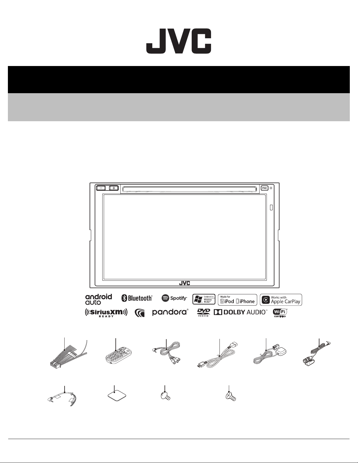
KW-V930BW (Australia) : X1
KW-V930BW (Other Areas) : M1
(3.5m)
Antenna
(QAL1550-001)
GPS Bracket
(LV45939-001A)
Screw (M5x8)
(QYSTSP5008ZA) x6
Screw (M5x8)
(QYSSSP5008ZA) x6
USB cord
(E3A-036x-00)
Car cable
(QAM1419-001)
(3m)
Microphone
(QAN0137-001)
Cord w.pinjack
(E3A-0274-00)
DC cord
(E3A-0214-00)
Remote control
(A7A-0006-00)
MA656<Rev.001>20174SERVICE MANUAL
KW-V830BT, KW-V930BW,
KW-V930BWM
MONITOR WITH DVD RECEIVER
COPYRIGHT © 2017 JVC KENWOOD Corporation
Lead free solder used in the board (material: Sn-Ag-Cu, melting point: 219 Centigrade)
Lead free solder used in the board (material: Sn-Cu, melting point: 230 Centigrade)
COPYRIGHT © 2017 JVC KENWOOD Corporation
No.MA656<Rev.001>
2017/4
Page 2
SPECIFICATION
Model for destination "K" (KW-V830BT)
Monitor section
Picture Size 6.75 inches (diagonal) wide
151.8 mm (W) 79.68 mm (H) (5-31/32 3-1/8 inch)
Display System TN LCD panel
Drive System TFT active matrix system
Number of Pixels 1 152 000 (800H 480V RGB)
Effective Pixels 99.99%
Pixel Arrangement RGB striped arrangement
Back Lighting LED
DVD player section
D/A Converter 24/32 bit
Audio Decoder Linear PCM/Dolby Digital/MP3/WMA/AAC/WAV/FLAC/Vorbis
Video Decoder MPEG1/MPEG2/MPEG4/WMV/H.264/MKV
Wow & Flutter Below Measurable Limit
Frequency
Response
Total Harmonic Distortion 0.010% (1 kHz)
S/N Ratio (dB) 90.5 dB
Dynamic Range 89 dB
Disc Format DVD-Video/VIDEO-CD/CD-DA/DVD-R/DVD-RW/DVD+R/DVD+RW
Sampling frequency 44.1/48/96 kHz
Quantifying Bit Number 16/20/24 bit
USB interface section
USB Standard USB 2.0 High Speed
File System FAT 16/ 32, exFAT, NTFS
Maximum Power Supply Current DC 5 V 1.5 A x 2
D/A Converter 24/32 bit
Audio Decoder MP3/ WMA/ AAC/ WAV/ FLAC/ Vorbis/ DSD
Video Decoder MPEG1/ MPEG2/ MPEG4/ WMV/ H.264/ MKV
Bluetooth section
Technology Bluetooth Ver.3.0
Frequency 2.402 GHz to 2.480 GHz
Output Power +4 dBm (MAX), 0 dBm (AVE), Power Class2
Maximum Communication range Line of sight approx. 10 m (32.8 ft)
Audio Codec SBC/AAC
Profile (Multi Profile support) HFP (V1.6) (Hands Free Profile), SPP (Serial Port Profile), A2DP (Ad-
96 kHz 20 Hz to 44 000 Hz
48 kHz 20 Hz to 22 000 Hz
44.1 kHz 20 Hz to 20 000 Hz
vanced Audio Distribution Profile), AVRCP (V1.5) (Audio/Video Remote
Control Profile), HID (Human Interface Device Profile), PBAP (Phonebook
Access Profile)
(No.MA656<Rev.001>)2/61
Page 3
FM tuner section
Frequency Range (step) 87.9 MHz to 107.9 MHz (200 kHz)
Usable Sensitivity (S/N: 30 dB) 9.3 dBf (0.8 V/75 )
Quieting Sensitivity (S/N: 50 dB) 15.2 dBf (1.6 V/75 )
Frequency Response 30 Hz to 15 kHz
S/N Ratio (dB) 75 dB (MONO)
Selectivity (± 400 kHz) Over 80 dB
Stereo Separation 45 dB (1 kHz)
AM tuner section
Frequency Range (step) 530 kHz to 1700 kHz (10 kHz)
Usable Sensitivity 29 dB
Video section
Color System of External Video Input NTSC
External Video Input Level (RCA jacks) 1 Vp-p/ 75
External Video Input Level (mini jack) 1 Vp-p/ 75
External Audio Max Input Level (mini jack) 2 V/ 25 k
Video Output Level (RCA jacks) 1 Vp-p/ 75
Audio Output Level (mini jack) 1.2 V/ 10 k
Audio section
Maximum Power (Front & Rear) 50 W 4
Full Bandwidth Power (Front & Rear) 22 W 4 (4, 14.4 V, at less than 1% THD)
Output frequency band 20 Hz to 88,000 Hz
Preout Level (V) 4 V/10 k
Preout Impedance 600
Speaker Impedance 4 to 8
DSP section
Graphics equalizer BAND 13 Band
Frequency (BAND1 to 13) 62.5/100/160/250/400/630/1k/1.6k/2.5k/4k/6.3k/10k/16k Hz
Q 1.35/1.5/2.0
Gain -9/-8/-7/-6/-5/-4/-3/-2/-1/0/1/2/3/4/5/6/7/8/9 dB
2 Way X'Over
High pass filter
2 Way X'Over
Low pass filter
3 Way X'Over
High pass filter
3 Way X'Over
Band pass filter
3 Way X'Over
Low pass filter
General
Operating Voltage 14.4 V (10.5 V to 16 V allowable)
Maximum Current Consumption 15 A
Installation Dimensions (W H D) 178 mm 100 mm 155 mm (7 3-15/16 6-1/8 inch)
Operational Temperature Range -10C to +60C
Weight 2.1 kg (4.63 lbs)
Frequency (Hz) Through, 30/40/50/60/70/80/90/100/120/150/180/220/250 Hz
Slope -6/-12/-18/-24 dB/Oct.
Frequency (Hz) 30/40/50/60/70/80/90/100/120/150/180/220/250 Hz, Through
Slope -6/-12/-18/-24 dB/Oct.
Frequency (Hz) 1k/1.6k/2.5k/4k/5k/6.3k/8k/10k/12.5k Hz
Slope -6/-12 dB/Oct.
Gain -8/-7/-6/-5/-4/-3/-2/-1/0 dB
Frequency (Hz) Through, 30/40/50/60/70/80/90/100/120/150/180/220/250 Hz
1k/1.6k/2.5k/4k/5k/6.3k/8k/10k/12.5kHz, Through
Slope -6/-12 dB/Oct.
Gain -8/-7/-6/-5/-4/-3/-2/-1/0 dB
Frequency (Hz) 30/40/50/60/70/80/90/100/120/150/180/220/250 Hz, Through
Slope -6/-12 dB/Oct.
Gain -8/-7/-6/-5/-4/-3/-2/-1/0 dB
• Design and specifications are subject to change without notice.
(No.MA656<Rev.001>)3/61
Page 4
SPECIFICATION
Models for destinations "M" & "X" (KW-V930BW, KW-V930BWM)
Monitor section
Picture Size 6.75 inches (diagonal) wide
151.8 mm (W) 79.68 mm (H)
Display System TN LCD panel
Drive System TFT active matrix system
Number of Pixels 1 152 000 (800H 480V RGB)
Effective Pixels 99.99%
Pixel Arrangement RGB striped arrangement
Back Lighting LED
DVD player section
D/A Converter 24/32 bit
Audio Decoder Linear PCM/Dolby Digital/MP3/WMA/AAC/WAV/FLAC/Vorbis
Video Decoder MPEG1/MPEG2/MPEG4/WMV/H.264/MKV
Wow & Flutter Below Measurable Limit
Frequency
Response
Total Harmonic Distortion 0.010% (1 kHz)
S/N Ratio (dB) 90.5 dB
Dynamic Range 89 dB
Disc Format DVD-Video/VIDEO-CD/CD-DA/DVD-R/DVD-RW/DVD+R/DVD+RW
Sampling frequency 44.1/48/96 kHz
Quantifying Bit Number 16/20/24 bit
USB interface section
USB Standard USB 2.0 High Speed
File System FAT 16/ 32, exFAT, NTFS
Maximum Power Supply Current DC 5 V 1.5 A x 2
D/A Converter 24/32 bit
Audio Decoder MP3/ WMA/ AAC/ WAV/ FLAC/ Vorbis/ DSD
Video Decoder MPEG1/ MPEG2/ MPEG4/ WMV/ H.264/ MKV
Miracast section
Mode Sink
Copyright protection HDCP2.2
Touch Control UIBC
Wi-Fi section
IEEE Standard Region 3/4: 802.11a/b/g/n, Region 2: 802.11b/g/n
Frequency Range Region 3/4: Dual Band (2.4GHz / 5GHz), Region 2: 2.4GHz
Channels Region 3/ 4: Auto (1-11ch), Auto (149,153,157,161ch), Region 2: Auto (1-
Transfer rates (MAX) 11a: 54 Mbps (Region 3/ 4), 11b: 11 Mbps, 11g: 54 Mbps, 11n: 150 Mbps
Output Power 11a: 14 dBm ± 2 dB (Region 3/ 4), 11b: 17 dBm ± 2 dB, 11g: 15 dBm ± 2
Bluetooth section
Technology Bluetooth Ver.3.0
Frequency 2.402 GHz to 2.480 GHz
Output Power +4 dBm (MAX), 0 dBm (AVE), Power Class2
Maximum Communication range Line of sight approx. 10 m (32.8 ft)
Audio Codec SBC/AAC
Profile (Multi Profile support) HFP (V1.6) (Hands Free Profile), SPP (Serial Port Profile), A2DP (Ad-
96 kHz 20 Hz to 44 000 Hz
48 kHz 20 Hz to 22 000 Hz
44.1 kHz 20 Hz to 20 000 Hz
11ch)
dB, 11n: 14 dBm ± 2 dB
vanced Audio Distribution Profile), AVRCP (V1.5) (Audio/Video Remote
Control Profile), PBAP (Phonebook Access Profile)
(No.MA656<Rev.001>)4/61
Page 5
FM tuner section
Frequency Range (step) 87.5 MHz to 108.0 MHz (50 kHz)
Usable Sensitivity (S/N: 30 dB) 9.3 dBf (0.8 V/75 )
Quieting Sensitivity (S/N: 46 dB) 15.2 dBf (1.6 V/75 )
Frequency Response 30 Hz to 15 kHz
Signal to Noise Ratio (dB) 75 dB (MONO)
Selectivity (± 400 kHz) Over 80 dB
Stereo Separation 45 dB (1 kHz)
AM tuner section
Frequency Range (step) Region 3/ 4: 531 kHz to 1611 kHz (9 kHz), Region 2: 531 kHz to1602 kHz
(9 kHz)
Usable Sensitivity Region 3/ 4: 28 dB, Region 2: 25 V
Video section
Color System of External Video Input NTSC/PAL
External Video Input Level (RCA jacks) 1 Vp-p/ 75
External Video Input Level (mini jack) 1 Vp-p/ 75
External Audio Max Input Level (mini jack) 2 V/ 25 k
Video Output Level (RCA jacks) 1 Vp-p/ 75
Audio Output Level (mini jack) 1.2 V/ 10 k
Audio section
Maximum Power (Front & Rear) 50 W 4
Full Bandwidth Power (Front & Rear) 22 W 4 (4, 14.4 V, at less than 1% THD)
Output frequency band 20 Hz to 88,000 Hz
Preout Level (V) 4 V/10 k
Preout Impedance 600
Speaker Impedance 4 to 8
DSP section
Graphics equalizer BAND 13 Band
Frequency (BAND1 to 13) 62.5/100/160/250/400/630/1k/1.6k/2.5k/4k/6.3k/10k/16k Hz
Q factor 1.35/1.5/2.0
Gain -9/-8/-7/-6/-5/-4/-3/-2/-1/0/1/2/3/4/5/6/7/8/9 dB
2 Way X'Over
High pass filter
2 Way X'Over
Low pass filter
3 Way X'Over
High pass filter
3 Way X'Over
Band pass filter
3 Way X'Over
Low pass filter
General
Operating Voltage 14.4 V (10.5 V to 16 V allowable)
Maximum Current Consumption 15 A
Installation Dimensions (W H D) 178 mm 100 mm 155 mm
Operational Temperature Range -10C to +60C
Weight 2.1 kg
• Design and specifications are subject to change without notice.
Frequency (Hz) Through, 30/40/50/60/70/80/90/100/120/150/180/220/250 Hz
Slope -6/-12/-18/-24 dB/Oct.
Frequency (Hz) 30/40/50/60/70/80/90/100/120/150/180/220/250 Hz, Through
Slope -6/-12/-18/-24 dB/Oct.
Frequency (Hz) 1k/1.6k/2.5k/4k/5k/6.3k/8k/10k/12.5k Hz
Slope -6/-12 dB/Oct.
Gain -8/-7/-6/-5/-4/-3/-2/-1/0 dB
Frequency (Hz) Through, 30/40/50/60/70/80/90/100/120/150/180/220/250 Hz
1k/1.6k/2.5k/4k/5k/6.3k/8k/10k/12.5kHz, Through
Slope -6/-12 dB/Oct.
Gain -8/-7/-6/-5/-4/-3/-2/-1/0 dB
Frequency (Hz) 30/40/50/60/70/80/90/100/120/150/180/220/250 Hz, Through
Slope -6/-12 dB/Oct.
Gain -8/-7/-6/-5/-4/-3/-2/-1/0 dB
(No.MA656<Rev.001>)5/61
Page 6
SECTION 1
PRECAUTION
1.1 Safety Precautions
(1) This design of this product contains special hardware and
many circuits and components specially for safety purposes. For continued protection, no changes should be made
to the original design unless authorized in writing by the
manufacturer. Replacement parts must be identical to
those used in the original circuits. Services should be performed by qualified personnel only.
(2) Alterations of the design or circuitry of the product should
not be made. Any design alterations of the product should
not be made. Any design alterations or additions will void
the manufacturers warranty and will further relieve the
manufacture of responsibility for personal injury or property
damage resulting therefrom.
(3) Many electrical and mechanical parts in the products have
special safety-related characteristics. These characteristics are often not evident from visual inspection nor can the
protection afforded by them necessarily be obtained by using replacement components rated for higher voltage, wattage, etc. Replacement parts which have these special
safety characteristics are identified in the Parts List of Service Manual. Electrical components having such features
are identified by shading on the schematics and by ( ) on
the Parts List in the Service Manual. The use of a substitute
replacement which does not have the same safety characteristics as the recommended replacement parts shown in
the Parts List of Service Manual may create shock, fire, or
other hazards.
(4) The leads in the products are routed and dressed with ties,
clamps, tubings, barriers and the like to be separated from
live parts, high temperature parts, moving parts and/or
sharp edges for the prevention of electric shock and fire
hazard. When service is required, the original lead routing
and dress should be observed, and it should be confirmed
that they have been returned to normal, after reassembling.
1.4 Critical parts for safety
In regard with component parts appearing on the silk-screen
printed side (parts side) of the PWB diagrams, the parts that are
printed over with black such as the resistor ( ), diode ( )
and ICP ( ) or identified by the " " mark nearby are critical
for safety. When replacing them, be sure to use the parts of the
same type and rating as specified by the manufacturer.
(This regulation dose not Except the J and C version)
1.5 Remote control
The Lithium battery is in danger of explosion if replaced incorrectly. Replace it only with the same or equivalent type.
1.6 Preventing static electricity
Electrostatic discharge (ESD), which occurs when static electricity stored in the body, fabric, etc. is discharged, can destroy the
laser diode in the traverse unit (optical pickup). Take care to prevent this when performing repairs.
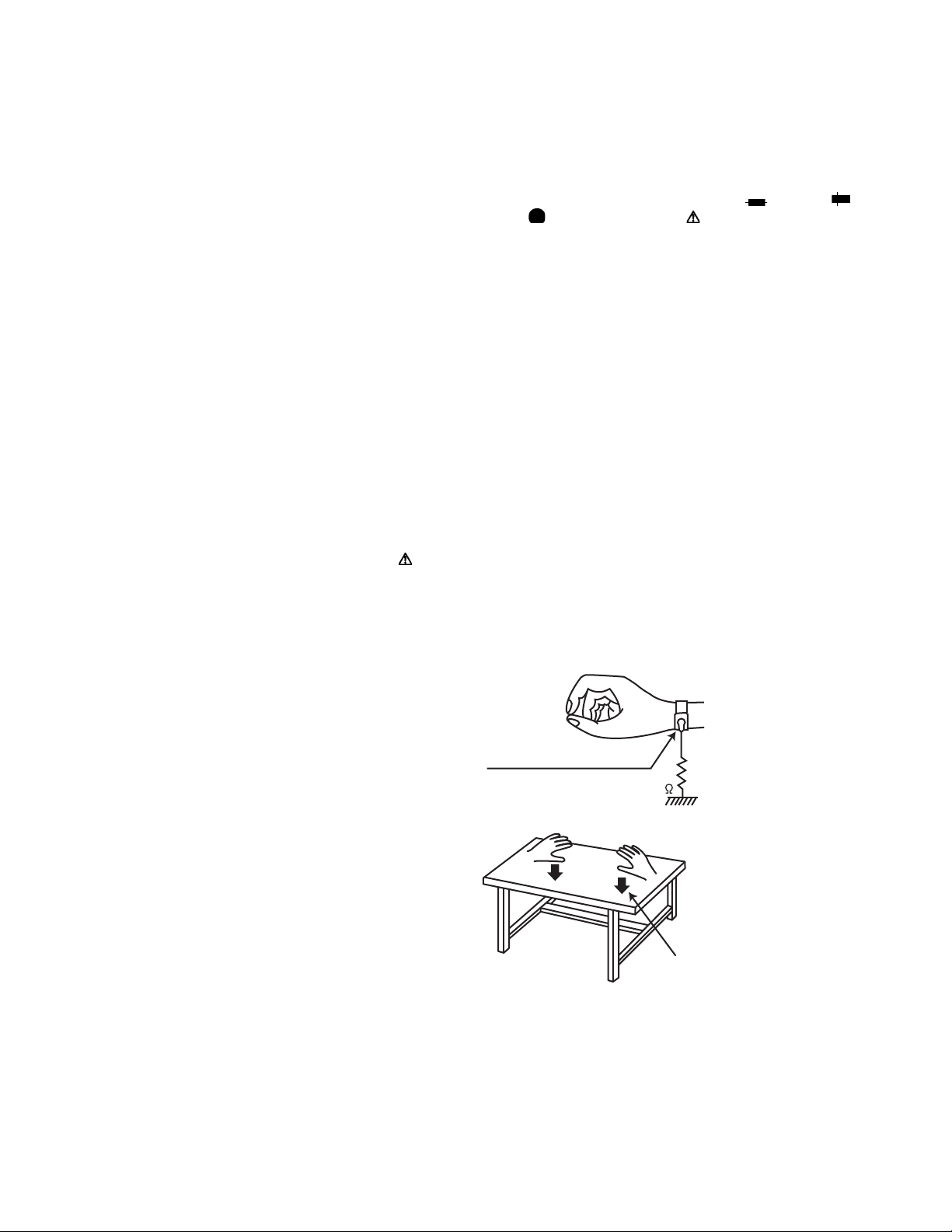
1.6.1 Grounding to prevent damage by static electricity
Static electricity in the work area can destroy the optical pickup
(laser diode) in devices such as laser products.
Be careful to use proper grounding in the area where repairs are
being performed.
(1) Ground the workbench
Ground the workbench by laying conductive material (such
as a conductive sheet) or an iron plate over it before placing the traverse unit (optical pickup) on it.
(2) Ground yourself
Use an anti-static wrist strap to release any static electricity
built up in your body.
(caption)
Anti-static wrist strap
1M
1.2 Warning
(1) This equipment has been designed and manufactured to
meet international safety standards.
(2) It is the legal responsibility of the repairer to ensure that
these safety standards are maintained.
(3) Repairs must be made in accordance with the relevant
safety standards.
(4) It is essential that safety critical components are replaced
by approved parts.
(5) If mains voltage selector is provided, check setting for local
voltage.
1.3 Caution
Burrs formed during molding may be left over on some parts
of the chassis.
Therefore, pay attention to such burrs in the case of preforming repair of this system.
(No.MA656<Rev.001>)6/61
Conductive material
(conductive sheet) or iron plate
(3) Handling the optical pickup
• In order to maintain quality during transport and before
installation, both sides of the laser diode on the replacement optical pickup are shorted. After replacement, return the shorted parts to their original condition.
(Refer to the text.)
• Do not use a tester to check the condition of the laser diode in the optical pickup. The tester's internal power
source can easily destroy the laser diode.
Page 7
1.7 Handling the traverse unit (optical pickup)
(1) Do not subject the traverse unit (optical pickup) to strong
shocks, as it is a sensitive, complex unit.
(2) Cut off the shorted part of the flexible cable using nippers,
etc. after replacing the optical pickup. For specific details,
refer to the replacement procedure in the text. Remove the
anti-static pin when replacing the traverse unit. Be careful
not to take too long a time when attaching it to the connector.
(3) Handle the flexible cable carefully as it may break when
subjected to strong force.
(4) I t is not possible to adjust the semi-fixed resistor that ad-
justs the laser power. Do not turn it.
1.8 Attention when traverse unit is decomposed
*Please refer to "Disassembly method" in the text for the
pickup unit.
• Apply solder to the short land sections before the FPC wire is
disconnected from the connector on the DVD mecha board. (If
the FPC wire is disconnected without applying solder, the pickup may be destroyed by static electricity.)
• In the assembly, be sure to remove solder from the short land
sections after connecting the FPC wire.
Short land section
(No.MA656<Rev.001>)7/61
Page 8

1.9 Important for laser products
1.CLASS 1 LASER PRODUCT
2.CAUTION :
(For U.S.A.) Visible and/or invisible class II laser radiation
when open. Do not stare into beam.
(Others) Visible and/or invisible class 1M laser radiation
when open. Do not view directly with optical instruments.
3.CAUTION : Visible and/or invisible laser radiation when
open and inter lock failed or defeated. Avoid direct
exposure to beam.
4.CAUTION : This laser product uses visible and/or invisible
laser radiation and is equipped with safety switches which
prevent emission of radiation when the drawer is open and
the safety interlocks have failed or are defeated. It is
dangerous to defeat the safety switches.
5.CAUTION : If safety switches malfunction, the laser is able
to function.
6.CAUTION : Use of controls, adjustments or performance of
procedures other than those specified here in may result in
hazardous radiation exposure.
!
Please use enough caution not to
see the beam directly or touch it
in case of an adjustment or operation
check.
(No.MA656<Rev.001>)8/61
Page 9

SECTION 2
SPECIFIC SERVICE INSTRUCTIONS
2.1 How to repair a fuse pattern
2.1.1 Purpose of fuse pattern
In order to prevent serious damage on the circuit, fuse pattern is prepared on the GND line of RCA Terminal. This damage may
take due to improper part replacement with a external equipment via RCA line.
2.1.2 Repair Procedure
(1) Check the shorted circuit at the meltdown point.
Need to clean up if the shorted circuit or carbonization happen at the fuse pattern.
(2) Add following part on the fuse pattern.
(3) Check output level.
Meltdown point
Part Number Part Name SPEC
F53-0513-08 PATTERN FUSE 4A
2.1.3 After finished repair
Due to improper part replacement, this meltdown occurs.
Thus please notice following information when the unit is returned to your customer.
Things to be checked before installing the unit.
(1) Check the GND line of external amplifier or other equipment which must connect properly.
(2) Check whether the GND line is not short-circuited with the battery terminal. (do not short-circuit these lines)
2.2 Precautions when replacing the IC
When A951(CIRCUIT MODULE) in MAIN PWB is defective, replace the whole MAIN PWB (CB-XJ1192***N).
2.3 Precautions when replacing the DIGITAL IO PWB
When DIGITAL IO PWB (DGB1/CB-XJA056***N) is replaced, it is necessary to set the region code.
2.4 Extension cable
• Purpose for this cable is checking the DIGITAL IO PWB and MAIN PWB.
• Parts number for this extension cable is "W3F-0291-00".
(No.MA656<Rev.001>)9/61
Page 10
2.5 Data storage content of ICs
PWB Ref No. Part name Data preservation contents (*Need to setting to after the replacement of IC)
MAIN PWB IC301 MAIN uCOM Error information
IC304 EEPROM *White balance adjustment value
*Tilt mecha Open / Clese position adjustment value
TunerSpan (Area) information
Image quality adjustment values
DC offset information
Tuner information
DIGITAL IO PWB IC503 NAND FLASH User configuration data
Camera setting data
Sound various setting data
BtPhone setting data
Use history data of the mechanical system
Play history data
Car Play setting
iPod setting data
*File that Garmin is using (except DDX and KW models)
IC525 eMMC *Serial No.
*Region information
User configuration data
Audio setting data
Phone book data
Telephone number preset data
*Production mode test result data
*Gesture factory setting data
Wallpaper customize data for DOP
*File that Garmin is using (except DDX and KW models)
Pairing device information that A&W SDK is using
Pairing device information managed by the BtBackEnd
logfile
*Garmin license file (except DDX and KW models)
Custom opening image
VIDEO PWB IC100 PANEL uCOM *VCOM data
*Key illumination white color adjustment value
2.6 Components description
2.6.1 MAIN PWB (XJ1-192)
Ref. No. Application / Function
IC31 5.1V DCDC converter DCDC converter IC
IC51 5.1V DCDC converter DCDC controller IC
IC52 AND GATE IC IC51 control
IC71 5.1V DCDC converter DCDC controller IC
IC91 5.1V DCDC converter DCDC controller IC
IC92 AND GATE IC IC91 control
IC110 OP Amp USB VBUS current detect
IC131 5.1V DCDC converter DCDC controller IC
IC132 AND GATE IC IC131 control
IC150 OP Amp USB VBUS current detect
IC201 Regulator 3.3V Regulator IC for XJ6
IC205 Regulator Regulator IC for D3.3V
IC206 Hi side SW MHL5V ON/OFF and current
IC207 Regulator Regulator IC for FAN9V
Operation / Condition / Compatibility
limit
(No.MA656<Rev.001>)10/61
Ref. No. Application / Function
IC301 Micro Computer Slave CPU of Telechips
IC302 Voltage Detecte IC RESET control
IC303 AND GATE IC Remote control input
IC304 E2PROM u-COM memory
IC305 Comparator RESET control
IC307 AND GATE IC TV remote control out
IC501 DSP AUDIO DSP DAC
IC502 Audio DAC Subwoofer out
IC503 Audio DAC Alter / NAVI out
IC506 Audio DAC 2 zone out
IC507 Regulator Regulator IC for A5V
IC508 Regulator Regulator IC for A3.3V
IC601 OP Amp MIC Amp
IC602 Regulator Regulator IC for MIC5V
IC651 AD converter ADC for NAVI audio input
Operation / Condition / Compatibility
Control of Power XJ6 etc.
Page 11
Ref. No. Application / Function
IC721 AND GATE IC Transform 5V to 3.3V for DASH
IC722 3state Buffer IC Transform 3.3V to 5V for DASH
IC731 AND GATE IC Transform 5V to 3.3V for
IC732 3state Buffer IC Transform 3.3V to 5V for
IC733 4state Buffer IC Remote out buffer for NAVI I/F
IC871 Video SW IC Composite signal selector
IC872 Regulator Regulator IC for V5V
IC921 Low Noise Amp Amp for GPS signal
IC922 Regulator Regulator IC for G3.3V
IC923 Regulator Regulator IC for BU1.8V
IC951 Regulator Regulator IC for BT3.3V/
A921 GPS module
A951 WiFI / BT Combo
module
Q1 FET 14V ON/OFF
Q3 Transistor Q1 control
Q4 Transistor BU voltage detect (Hi voltage)
Q5 Transistor BU voltage detect (Hi voltage)
Q6 Transistor BU voltage detect (Hi voltage)
Q7 Transistor BU voltage detect (Low voltage)
Q8 Transistor BU voltage detect (Low voltage)
Q9 Transistor BU voltage detect (Hi voltage)
Q10 Transistor BU voltage detect (Low voltage)
Q11 Transistor BU voltage detect (8.5V)
Q12 Transistor BU voltage detect (8.5V)
Q51 Transistor IC51 EN control
Q52 Transistor IC51 EN control
Q110 Transistor QUICK CHARGE detect out
Q111 Transistor QUICK CHARGE detect
Q112 Transistor VBUS1 over current detect
Q113 Transistor VBUS1 over current detect
Q114 Transistor VBUS1 over current detect out
Q115 Transistor VBUS1 over current detect out
Q116 Transistor IC91 EN control
Q117 Transistor IC91 EN control
Q131 Transistor VBUS2 over voltage detect out
Q150 Transistor QUICK CHARGE detect out
Q151 Transistor QUICK CHARGE detect
Q152 Transistor VBUS2 over current detect
Q153 Transistor VBUS2 over current detect
Q154 Transistor VBUS2 over current detect out
Operation / Condition / Compatibility
CAM I/F
CAM I/F
iDATA LINK I/F or NAVI I/F
iDATA LINK I/F or NAVI I/F
WiFi3.6V
control
control
Ref. No. Application / Function
Q155 Transistor VBUS2 over current detect out
Q156 Transistor IC131 EN control
Q157 Transistor IC131 EN control
Q301 Transistor SW3.3V control
Q302 Transistor Q301 control
Q303 Transistor u-COM RESET control
Q304 Transistor u-COM RESET control
Q305 Transistor u-COM RESET control
Q306 Transistor DET_MUTE control
Q307 Transistor DET_MUTE control
Q308 Transistor SI control
Q309 Transistor SI control
Q312 Transistor PCON/ANT out
Q313 Transistor PCON/ANT voltage control
Q314 Transistor PCON/ANT voltage control
Q315 Transistor u-COM RESET control
Q316 Transistor u-COM RESET control
Q317 Transistor u-COM RESET control
Q318 Transistor u-COM RESET control
Q319 Transistor u-COM RESET control
Q501 Transistor DSP power down control
Q502 Transistor DAC RESET control
Q651 Transistor ADC power down control
Q801 FET STE REMO Pull up SW
Q802 FET STE REMO Pull up SW
Q803 Transistor STE REMO Pull up control
Q921 Transistor G3.3V control
Q922 Transistor BU1.8V control
Operation / Condition / Compatibility
(No.MA656<Rev.001>)11/61
Page 12
2.6.2 DIGITAL IO PWB (XJA-056)
Ref. No. Application / Function
IC501 SoC Processor for Digital Media
IC503 2Gb SLC NAND
Flash memory
IC525 16GB or 8GB or 4GB
eMMC memory
IC531 4Gb x16 DDR3
memory
IC532 4Gb x16 DDR3
memory
IC546 AND Logiv IC Rear camera control
IC541 LCD Controller Video scaler and timing
IC543 Dual Bus Switch I2C SW
IC544 AND Logiv IC Rear camera control
IC545 OR Logic IC Rear camera control
IC563 iPod Authentication
Coprocessor
IC571 USB Charging Port
Controller
IC573 2port USB Hub IC 2port USB Hub
IC574 Regulator D+1.2V_HUB Regulater IC
IC591 DCDC controller IC 3.3V DCDC converter
IC592 DCDC controller IC 1.17V DCDC converter
IC593 Regulator SD+3.3V Regulater IC
IC594 Regulator D+2.5V Regulater IC
IC595 Regulator D+1.8V Regulater IC
IC596 Regulator CPU+1.5V Regulater IC
IC597 Regulator TCON+1.5V Regulater IC
IC598 Hi side SW Over current protection of
IC599 Hi side SW Over current protection of
IC600 Hi side SW Over current protection of
IC601 DCDC controller IC 1.23V DCDC converter
IC602 AND Logiv IC IC591 control
IC631 Video Amp IC with
LPF
IC651 Differential serial
interface IC
Q5401 Transistor Emitter follower circuit of DVD
Q5402 Transistor Emitter follower circuit of DVD
Q5403 Transistor Emitter follower circuit of DVD
Q5603 Transistor IC563 control
Q5604 Transistor IC563 control
Q5605 Transistor IC563 control
Operation / Condition / Compatibility
SoC program memory
NAVI MAP memory
For SoC memory
For SoC memory
controller
iPod Authentication
USB charging port control
BL+5V
PANEL+5V
PANEL+3.3V
SoC Video amplifier and LPF
Serialize output of IC541(RGB)
line(Y)
line(Cb)
line(Cr).
Ref. No. Application / Function
Q5606 Transistor IC563 control
Q5607 Transistor IC563 control
Q5608 Transistor IC563 control
Q5801 Transistor MHL VBUS Control SW
Q5901 Transistor IC593 control
Q5902 Transistor IC593 control
Q6301 Transistor UPDATE Control SW
2.6.3 AUDIO PWB (XJ6-105)
Ref. No. Application / Function
IC1 Multi channel Voltage
Regulator
IC41 Voltage Regulator BU3.3V
IC42 Voltage Regulator A8.5V for XJ6
IC101 Power IC Power AMP
IC115 OR Logic IC PWIC_BEEP_Level_shift
IC201 Electoric Vol IC Audio Vol Control, Audio Signal
IC260 Analog IC Audio Select for SXM/ADS
IC261 Analog IC ISO Amp for DVD
IC301 Voltage Regulator RF3.3V
IC361 Microprocessor Microprocessor for DAB
IC401 FM & RDS Receiver Tuner for TMC
IC511 OR Logic IC SXi_TX Level shift
IC512 OR Logic IC SXi_RX Level shift
IC590 Bus Buffer IC Buffer for TV_Remote_Out
IC601 Line amp IC 5V Preout
IC781 Motor Drv Monitor mecha slide motor
IC790 Voltage Regulator TILT9.7V
IC801 speech synthesis LSI Audio for Emotional Beep
IC802 operational amplifier Change audio signal from
IC803 operational amplifier Mix Beep with audio for preout
IC900 Voltage Regulator DAB3.3V
IC1101 operational amplifier audio buffer to PWIC
IC1102 operational amplifier audio buffer to PWIC
Q31 Transistor ACC Detect
Q32 Transistor ACC Detect
Q51 DIGI Transistor Illumi Detect
Q60 DIGI Transistor Camera control
Q61 DIGI Transistor Camera control
Q62 DIGI Transistor Camera control
Q63 DIGI Transistor Camera control
Q80 DIGI Transistor Parking Detect
Q81 Transistor Parking Detect
Q82 Transistor Parking Detect
Operation / Condition / Compatibility
Operation / Condition / Compatibility
ILM8VCD8VA8.5VSW5VBU5V
P-CONP-ANT Power Supply
Select
module
control
differential to single end
(No.MA656<Rev.001>)12/61
Page 13
Ref. No. Application / Function
Q90 DIGI Transistor Reverse Detect
Q96 Transistor Update Detect
Q151 DIGI Transistor Preout mute drive
Q152 DIGI Transistor Preout mute drive
Q155 DIGI Transistor Preout mute drive
Q156 DIGI Transistor Preout mute drive
Q161 DIGI Transistor Preout FL mute
Q162 DIGI Transistor Preout FR mute
Q163 DIGI Transistor Preout RL mute
Q164 DIGI Transistor Preout RR mute
Q165 DIGI Transistor Preout SWL mute
Q191 DIGI Transistor AVOUT mute drive
Q193 DIGI Transistor AVOUT AL mute
Q194 DIGI Transistor AVOUT AR mute
Q391 DIGI Transistor DAB ANT POWER
Q392 DIGI Transistor DAB ANT POWER control
Q451 DIGI Transistor ANT Distributer
Q781 DIGI Transistor MOTOR Drv [IC781] Power
Q801 DIGI Transistor PDN for IC801
2.6.4 VIDEO PWB (XJ8-043)
Ref. No. Application / Function
IC100 MCU IC Panel uCOM
IC102 Analog IC RESET Voltage detedt 2.8V
IC103 IC 3.3V Regulator
IC106 MOS IC Inverter
IC200 IC LCD Backlight power LCD
IC201 MOS IC Inverter
IC202 MOS IC 3.3V Regulator
IC300 SV-analogue IC 10.5V Regulator
IC400 MOS IC LVDS Reciever
IC800 IR detect unit REMOCON IC
Q100 DIGI Transistor Reset Voltage Out
Q101 DIGI Transistor Reset Voltage Out
Q200 DIGI Transistor Backlight turn off by [V_OFF]
Q201 Transistor Luminance of Backlight
Q202 MOS FET SW control for Backlight Power
Q203 Transistor DCDC IC control by
Q204 Transistor Backlight LED Driver
Q205 Transistor Backlight LED Driver
Q206 Transistor Backlight LED Driver
Q207 Transistor Luminance of Backlight
Q208 Transistor Backlight LED Driver
Operation / Condition / Compatibility
Supply
Operation / Condition / Compatibility
power LED power supply
Contorol
[BOOST_H]
Contorol
Ref. No. Application / Function
Q209 Transistor Backlight LED Driver
Q210 Transistor Backlight LED Driver
Q211 Transistor Backlight LED Driver
Q212 Transistor Backlight LED Driver
Q213 DIGI Transistor Backlight turn off by [V_OFF]
Q214 DIGI Transistor Backlight turn off by [V_OFF]
Q300 Transistor 13V Soft Start SW
Q301 Transistor 20V Soft Start SW
Q302 Transistor 20V Regulete
Q303 DIGI Transistor 13V Soft Start SW
Q304 DIGI Transistor 20V Soft Start SW
Q305 DIGI Transistor 13V Soft Start SW
Q306 DIGI Transistor 20V Soft Start SW
Q307 Transistor -7V Soft Start SW
Q308 Transistor -7V Soft Start SW
Q309 Transistor -7V Regulate
Q310 DIGI Transistor -7V Regulate
Q311 DIGI Transistor -7V Regulate
Q313 Transistor 15V Regulate
Q400 Transistor VCOM Voltage Driver
Q401 Transistor VCOM Voltage Driver
Q402 DIGI Transistor VCOM Voltage Driver
Q403 DIGI Transistor VCOM Voltage Driver
Q404 DIGI Transistor VCOM Voltage Driver
Q405 DIGI Transistor VCOM Voltage Driver
Q500 Transistor Touch Panel Control
Q501 Transistor Touch Panel Control
Q502 Transistor Touch Panel Control
Q503 Transistor Touch Panel Control
Q504 DIGI Transistor Touch Panel Control
Q505 Transistor Touch Panel Control
Q506 Transistor Touch Panel Control
Q800 Transistor White LED Driver
Q801 Transistor White LED Driver
2.6.5 BLUETOOTH PWB (XJ9-017)
Ref. No. Application / Function
A951 Cuicuit Module BT Module
Operation / Condition / Compatibility
Operation / Condition / Compatibility
(No.MA656<Rev.001>)13/61
Page 14

2.7 Microcomputer's terminal description
2.7.1 Main microcomputer (MAIN PWB : IC301)
Pin
No.
1VREF -
2 AVCC -
3 D_TO_M_DAT I DSP (AK7738) data communication (DSP to
4 M_TO_D_DAT O DSP (AK7738) data communication (MAIN to
5 M_TO_D_CLK O DSP (AK7738) clock communication (MAIN to
6 PWIC_BEEP O PWIC BEEP PWM output 1k/2 kHz duty 50%
7 REMO I Wired REMO data input For KWD models
8 M_TO_N_DAT O NAVI data communication (MAIN to NAVI)
9 N_TO_M_DAT I NAVI data communication (NAVI to MAIN)
10 M_TO_N_CLK O NAVI clock communication (MAIN to NAVI)
11 TOUCH_TV_REMO O REMO OUT of general-purpose TV CTRL touch
12 D3_3V_CTL O DIGITAL IO PWB D3.3 V control H: ON, L: OFF
13 BYTE - External data bus width switching input (In single
14 CNVSS - Processor mode switching terminal In microprocessor mode: Connected to
15 XCIN - Sub clock oscillation circuit input 32.768kHz (Crystal oscillator)
16 XCOUT - Sub clock oscillation circuit output 32.768kHz (Crystal oscillator)
17 /RESET I Reset input L: RESET on, H: Reset clear
18 XOUT - Main clock oscillation circuit output 16MHz (Crystal oscillator)
19 VSS -
20 XIN - Main clock oscillation circuit input 16MHz (Crystal oscillator)
21 VCC1 -
22 NMI I
23 DAB_SREQ I DAB ucom to Syscom REQ DAB model only
24 /N_TO_M_REQ I NAVI data receiving request (NAVI to MAIN)
25 /N_TO_M_RDY I NAVI data transmission and receiving enable sig-
26 /M_TO_N_REQ O NAVI data transmission request (MAIN to NAVI)
27 D_REC_RX I RX between SYS and drive recorder
28 /NAVI_RST O NAVI reset (MAIN to NAVI)
29 D_REC_TX O TX between SYS and drive recorder
30 NC I
31 VF_CTL+ O Frequency control of the DC-DC_IC, 180 degrees
32 NC I
33 A_POWER_PWM O Frequency control of XJ6_5V PREOUT_IC
34 WREMO_J I
35 VF_CTL- O Frequency control of the DC-DC_IC, 180 degrees
Pin Name I/O Application Processing/Operation/Description
MAIN)
DSP) Shared with ADC data communication
DSP) Shared with ADC data communication
H: Except REMO OUT
panel operation
In single chip mode: Connected to VSS
chip mode: Connected to VSS)
VCC1
In single chip mode: Connected to VSS
nal (NAVI to MAIN)
phase of VF_CTL-
phase of VF_CTL+
(No.MA656<Rev.001>)14/61
Page 15
Pin
No.
36 I2C_SDA_DISP
37 VCC1 -
38 I2C_SCL_DISP
39 VSS -
40 DEBUG_SCLK I Clock synchronous serial communication In standard serial I/O mode1: CLK
41 BUSY O BUSY signal output terminal In standard serial I/O mode1
42 TUN_SDA I/O DATA of between the SYS and HELIO
43 TUN_SCL O CLK of between the SYS and HELIO
44 NC O L fixed
45 NC O L fixed
46 SOC_RST
47 FAN_CTL O L fixed (FAN voltage changing standby terminal) H: high voltage, L: constant voltage
48 DAC_PDN O DAC power down H: Power down at the same timing as
49 /M_TO_AD_CSN O ADC control L: active
50 HOME I HOME KEY L: Depression of HOME KEY is detected
51 POW_REG
52 EPM I Standard serial I/O mode 1 Fixed connection to VSS
53 POW_ON O SW power supply ON/OFF control H: ON, L: OFF
54 EPROM_SCL O E2PROM SCL
55 EPROM_SDA I/O E2PROM SDA
56 EPROM_WC O E2PROM write protection H: Write prohibited, L: Write enable
57 Q_CHG I Quick charge detection L: Detected, H: Normal
58 DABUCOM_RST O DAB uCOM reset control L: RESET on, H: Reset clear
59 POW_AMP
60 REAR_CAM_PON O RCAM power enable L fixed
61 CE I Standard serial I/O mode 1 Fixed connection to VSS
62 LCD_MUTE2 O Insert black picture when rear camera switching
63 DABUCOM_POW O DAB uCOM startup request (DAB model only) H: Startup, L: Shutdown
64 CAYMAN_MREQ
64 CAYMAN_MREQ
65 CAYMAN_MDATA
Pin Name I/O Application Processing/Operation/Description
(VF_SW)
(VF_SW2)
(UPDATE_OUT)
(SW14V_PON)
(PWIC_STBY)
%CAYMAN_MREQ%
%HD_CS%
%DAB_MC_DATA%
O DATA of between the SYS and PANEL/decoder-
PANEL power PWM control
O CLK of between the SYS and PANEL/decoder-
PANEL power PWM control
O Forced write notification to Telechips When detecting L for more than 1 second at
O SW14V ON/OFF H: ON L: OFF
O Power IC standby control H: ON, L: OFF
O SYS to DAB uCOM REQ DAB model only
O SYS to CAYMAN REQ HD model only
O MCDATA of between the SYS and DAB DAB model only
Fast start: I2C communication
Normal operation: PWM control
In standard serial I/O mode 1: TX
For software rewriting
Fast start: I2C communication
Normal operation: PWM control
In standard serial I/O mode 1: RX
For software rewriting
For software rewriting
107 pin, H output
M_TO_D_PDN
For software rewriting
DOP model only
For rewriting software
DAB model only
(No.MA656<Rev.001>)15/61
Page 16
Pin
No.
65 CAYMAN_MDATA
66 CAYMAN_SDATA
66 CAYMAN_SDATA
67 CAYMAN_MCLK
67 CAYMAN_MCLK
68 EVOL_MUTE_M O EVOL MUTE control L:ON, H:OFF
69 EVOL_MUTE_S O EVOL MUTE control L:ON, H:OFF
70 GPS_RESET O GPS reset H: reset
71 EVOL_MUTE2 O E-VOL SW mute L:ON, H:OFF
72 SW_REVERSE_NAVI O Reverse detection notice (MAIN to NAVI) H: Fast startup, L: Reverse Detected
73 TILT_SPEED O Power supply voltage switching of tilt mechanism control start after PON
74 TMOTOR_P O Tilt control of tilt mecha control start after PON
75 TMOTOR_M O Tilt control of tilt mecha control start after PON
76 MUTE_AMP O Power IC audio mute control H: OFF, L: ON
77 PS3_BATLOW
78 NAVI_NMIPDN O NAVI power down L: Power down
79 TUN_RST O RESET of HELIO L: RESET on, H: Reset clear
80 BUZ_SCL O CLK of beep IC I2C communication
81 BUZ_SDA O DATA of beep IC I2C communication
82 BUZ_BUSY I Beep IC communication BUSY input (0=audio
83 EVOL_MUTE1 O E-VOL rear mute L: ON, H: OFF
84 EVOL_MUTE0 O E-VOL front mute L: ON, H: OFF
85 VCC2 -
86 PRE_MUTE_FR O Pre-out mute (for the front rear) L: OFF, H: ON
87 VSS -
88 NC (VSP_DA) O L fixed
89 PS1_ACC I ACC detection H: ACC power reduction detected, L: normal
90 PS2_BAT (BU_DET_7) I Backup power supply detection H: Backup power reduction detected, L: nor-
91 PANEL_DET_A I PANEL detachable detection
92 SECURE_CTL (SI) O SI control
93 SW_PARKING I Parking detection H: Detection L: Running
94 SW_REVERSE I Reverse detection L: Detected, H: Normal
95 SW_ILLMI I Illumi detection L: ON (detected), H: OFF (not detected)
96 PRE_MUTE_SW O Pre-out mute (for the subwoofer) L: ON, H: OFF
97 SI_ADJ O SI Dimmer control
98 SW_A I Panel release key detection
Pin Name I/O Application Processing/Operation/Description
O MCDATA of between the SYS and CAYMAN HD model only
%HD_MC_DATA%
I SCDATA of between the SYS and DAB DAB model only
%DAB_SC_DATA%
I SCDATA of between the SYS and CAYMAN HD model only
%HD_SC_DATA%
O CLK of between the SYS and DAB DAB model only
%DAB_MCLK%
O CLK of between the SYS and CAYMAN HD model only
%HD_MCLK%
L fixed when become to be able to communicate with Telechips
I Backup power detection H: backup power reduction detected
(BU_DET_9)
output/disconnection detected)
L: normal
Setting data retransmission to EVOL with HI
to LO return, Detecting PRE_MUTE ON
H: not in operation, L: in audio output
mal
(No.MA656<Rev.001>)16/61
Page 17
Pin
No.
99 STEREMO_SW O Select of STEREMO pull-up resistor H: 460 ohm (Toyota, Daihatsu, Nissan, Maz-
100 CAMERA_TXD O CMOS camera communication (UART TX)
101 CAMERA_RXD O CMOS camera communication (UART RX)
102 EVOL_SCL I/O CLK of between the SYS and EVOL
103 EVOL_SDA O DATA of between the SYS and EVOL
104 PWIC_CDET I PWIC short detection H: Normal, L: Abnormal
105 TYPE2 I Destination setting2
106 LINE_MUTE I LINE-MUTE input detection 1.6V: Normal
107 UPDATE_DET I SoC forced update mode detection When L is detected for 1 second or longer,
108 AD_TILT_DET I Panel mecha tilt detection
109 MODEL_1 I Model setting1
110 MODEL_0 I Model setting0
111 AD_DCERR I DC offset detection of SP output L: Detected
112 DSP_PDN O DSP power down H: Power down
113 PCON/ANT1 O PCON/ANT_CON/X34 power control
114 PCON/ANT2 O PCON/ANT_CON/X34 power control
115 PCON/ANT3 O PCON/ANT_CON/X34 power control
116 DSP_CSN O DSP chip selector (MAIN to DSP) L: between the microcomputer communica-
117 PANEL_VCC_OFF O ON/OFF control of power supply to PANEL H: ON, L: OFF
118 NC O L fixed
119 ILLMI_CTRL
120 ASEL O Audio selector CH switching
121 NC (PGOOD) O L fixed
122 NC O L fixed
123 NC(TYPE_OEM) O L fixed (reserved for DOP)
124 STE1 I Steering remote control KEY1 input
125 STE2 I Steering remote control KEY2 input
126 TYPE_1 I Destination setting1
127 AVSS -
128 TYPE_0 I Destination setting0
Pin Name I/O Application Processing/Operation/Description
da, Honda, Subaru), L: 4.7k ohm (Mitsubishi)
1V or less: AUDIO MUTE, Transition to Call
interrupt screen
2.0V or more: AUDIO ATT
46 pin to H output
tion
O ON/OFF control of DISC LED H: ON, L: OFF
(SLOT_ILL)
(No.MA656<Rev.001>)17/61
Page 18
2.7.2 Panel microcomputer (VIDEO PWB : IC100)
Pin
No.
1NC -
2NC -
3NC -
4 LCD_18V O LCD power supply control 2 LCD_ENA_18V
5 LCD_-6V O LCD power supply control 1 LCD_ENA_-6V
6 /RESET I System reset input
7VOFF OVOFF
8 FLMD0_CTRL O FLMD0 terminal control For self-programming
9 FLMD0 I Pull-in flash programming clock mode
10 EX_X2 O For flash programmer
11 NC -
12 REGC - Regulator output stabilization capacitor connec-
13 VSS - Ground for ports other than P121-P124
14 EVSS - Ground for ports other than P20-P27, P121-P124
15 VDD - Positive power supply for ports other than P121-
16 EVDD - Positive power supply for ports other than P20-
17 VF_SW2 I BOOST SYNC frequency for switching For rear camera quick start-up
18 VF_SW I BOOST SYNC frequency for switching For rear camera quick start-up
19 /P_TO_N_REQ O Transmission request to NAVI of communication
20 /N_TO_P_REQ I Clock output request from NAVI of communica-
21 BL_PWM O PWM output for brightness change of the LCD
22 NC -
23 NC -
24 LCD_9.2V O LCD power supply control 3 LCD_ENA_9.2V
25 V-COM1 O V-COM voltage adjustment 1
26 V-COM2 O V-COM voltage adjustment 2
27 V-COM3 O V-COM voltage adjustment 3
28 V-COM4 O V-COM voltage adjustment 4
29 BOOST_H O LCD backlight MST_BOOST_ENA
30 NC -
31 NC -
32 NC -
33 NC -
34 R_VOL+ I Rotary VOL
35 R_VOL- I Rotary VOL
36 MENU I MENU key
37 KEY_ILL O EJECT for Illumination red dimming
38 /N_TO_P_RDY I State notification from NAVI of communication
39 KEY_PWM_R O Key llumination PWM RED
Pin Name I/O Application Processing/Operation/Description
tion for internal operation
P124
P27, P121-P124
between the microcomputer
tion between the microcomputer
BL_PWM
backlight
between the microcomputer
(No.MA656<Rev.001>)18/61
Page 19
Pin
No.
40 KEY_PWM_G O Key llumination PWM GREEN/White LED DIMMER
41 KEY_PWM_B O Key llumination PWM BLUE/White LED ON
42 RXD O For communication with the flash writer
43 TXD O For communication with the flash writer
44 P_TO_N_DAT O Data transmission to the NAVI of communication
45 N_TO_P_DAT I Data received from NAVI of communication be-
46 P_TO_N_CLK O Clock signal to the NAVI of communication be-
47 AVREF - Analog reference voltage input
48 AVSS - Analog GND
49 NC -
50 KEY2 I Tact switch voltage input 2
51 KEY1 I Tact switch voltage input 1 EJECT Key
52 KEY3 I Tact switch voltage input 3 For VW
53 XDATA_U I Touch panel X-axis voltage input VDD side
54 XDATA_D I Touch panel X-axis voltage input GND side
55 YDATA_U I Touch panel Y-axis voltage input VDD side
56 YDATA_D I Touch panel Y-axis voltage input GND side
57 X0 O Touch panel X-axis control
58 X1 O Touch panel X-axis control
59 Y0 O Touch panel Y-axis control
60 Y1 O Touch panel Y-axis control
61 BOOST_SYNC O BOOST_SYNC
62 TP_PRESS O Touch panel control
63 PULL_UP_ON O Touch panel control
64 NC -
Pin Name I/O Application Processing/Operation/Description
between the microcomputer
tween the microcomputer
tween the microcomputer
(No.MA656<Rev.001>)19/61
Page 20

SECTION 3
DISASSEMBLY
3.1 Main body
3.1.1 Removing the VIDEO PWB (See Fig.1 to 2)
(1) Remove the 5 screws (a,b). (See Fig.1)
(2) Remove 3 hooks, and remove the FRONT PANEL ASS'Y.
(See Fig.1)
(3) Disconnect the FFC wire from the connector. (See Fig.1)
b
FRONT PANEL ASS'Y
b
a
CN1
a
: Hook position
Fig.1
(4) Disconnect the each wires from connectors. (See Fig.2)
(5) Remove the 4 screws (a), and remove the VIDEO PWB (1/2).
(See Fig.2)
(6) Remove the 1 screw (b), and remove the VIDEO PWB (2/2).
(See Fig.2)
a
b
a
3.1.2 Removing the DVD MECHA ASS'Y (See Fig.3)
(1) Remove the 6 screws (a), and remove the TOP PLATE.
(2) Remove the DVD MECHA ASS'Y, and disconnect the each
wires from connectors.
(3) Remove the 4 screws (b), and remove the BRACKET.
a
a
a
a
a
BRACKET
b
CN572
b
CN751
TOP PLATE
a
a
b
BRACKET
DVD MECHA ASS'Y
b
CN800
VIDEO PWB (2/2)
VIDEO PWB (1/2)
CN400
Fig.2
a
a
CN500
(No.MA656<Rev.001>)20/61
Fig.3
Page 21

3.1.3 Removing the DIGITAL IO PWB (See Fig.4)
(1) Disconnect the each wires from connectors.
(2) Remove the 4 screws, and remove the HEAT SINK.
(3) Remove the DIGITAL IO PWB.
3.1.5 Removing the MAIN PWB (See Fig.6 and 7)
(1) Disconnect the each wires from connectors. (See Fig.6)
(2) Remove the 6 screws, and remove the REAR PANEL.
(See Fig.6)
HEAT SINK
CN562
CN571
DIGITAL IO PWB
Fig.4
3.1.4 Removing the BLUETOOTH PWB (See Fig.5)
(1) Disconnect the FFC wire from connector.
(2) Remove the 2 screws, and remove the BLUETOOTH
PWB.
REAR PANEL
CN251
CN201
CN802
Fig.6
(3) Disconnect the each wires from connectors. (See Fig.7)
(4) Remove the 3 screws (a), and remove the BRACKET. (See
Fig.7)
(5) Remove the 4 screws (b), and remove the MAIN PWB.
(See Fig.7)
a
BRACKET
CN952
BLUETOOTH PWB
Fig.5
b
CN1
CN301
CN201
b
a
MAIN PWB
Fig.7
a
b
b
(No.MA656<Rev.001>)21/61
Page 22

3.1.6 Removing the AUDIO PWB (See Fig.8 to 10)
(6) Remove the 9 screws, and remove the SIDE PLATE. (See
Fig.8)
SIDE PLATE
(8) Remove the 4 screws, and remove the AUDIO PWB. (See
Fig.10)
SIDE PLATE
Fig.8
(7) Remove the 3 screws, and remove CHASSIS. (See Fig.9)
CHASSIS
Fig.9
AUDIO PWB
Fig.10
(No.MA656<Rev.001>)22/61
Page 23

3.2 DVD mechanism assembly
TOP CHASSIS ASS'Y
3.2.1 Removing the PHOTO PWB (See Fig.1 to 3)
(1) Remove the 4 screws, and remove the TOP CHASSIS
ASS’Y. (See Fig.1)
Fig.1
(2) Remove the solder, and remove the wires. (See Fig.2)
3.2.2 Removing the Roller arm assy (See Fig4)
(1) Remove the ROLLER SPRING in the direction of the arrow.
(2) Remove the 1 screw, and remove the ROLLER ARM
ASS’Y.
ROLLER SPRING
ROLLER ARM ASS'Y
Fig.4
3.2.3 Removing the Clamp arm assy (See Fig.5)
(1) Remove the Clamp spring in the direction of the arrow.
(2) Remove the Clamp arm assy.
CLAMP ARM ASSY
BLACK WIRE
YELLOW WIRE
ORANGE WIRE
Fig.2
(3) Remove the 1 screw, and remove the PHOTO PWB.
(See Fig.3)
Note: When removing the PHOTO PWB,
be careful not to touch the photo sensor.
PHOTO PWB
CLAMP SPRING
Fig.5
3.2.4 Removing the TM ASSY and DVD MECHA PWB
(See Fig.6,7)
(1) Remove the solder, and remove the wires. (See Fig.6)
(2) Remove the 4 screws, and remove TM ASS’Y. (See Fig.6)
(3) Remove the 2 screws, and remove the DVD MECHA PWB.
(See Fig.6)
TM ASS'Y
Fig.3
BLACK WIRE
RED WIRE
(No.MA656<Rev.001>)23/61
DVD MECHA PWB
Fig.6
Page 24

(4) Solder the short land on the FPC wire. (See Fig.7)
TM ASS'Y
SHORT LAND
DVD MECHA PWB
LOADING MOTOR BRACKET ASS'Y
(5) Disconnect the FPC wires form the connectors. (See Fig.7)
Fig.7
3.2.5 Removing the Loading motor (See Fig.8 to 11)
(1) Remove the 2 screws, and remove the LOADING MOTOR
BRACKET ASS’Y. (See Fig.8)
(4) Remove the 2 screws, and remove the GEARBOX ASS’Y.
(See Fig.10)
Fig.10
(5) Remove the 2 screws, and remove the LOADING MOTOR.
(See Fig.11)
LOADING MOTOR
Fig.8
(2) Remove the SLIDER SPRING in the direction of the arrow.
(See Fig.9)
(3) Remove the the SLIDER. (See Fig.9)
SLIDER SPRING
SLIDER
Fig.9
Fig.11
(No.MA656<Rev.001>)24/61
Page 25

SECTION 4
ADJUSTMENT
4.1 Special Mode and Specoal operation List
Mode Name Description Prerequisite Operation
Force EJECT Forced EJECT mode for when DISC
cannot be taken out.
TUNER span
switching
Opening screen /
wallpaper / initial
settings / steering
remote control set
rewrite mode
(Customize Menu)
Production Menu Special function menu for the
Service Menu Special function menu used by
Initialize Factory
Default
Forced Security
Release
For switching the frequency step /
span of TUNER
For rewriting the configurations of
the Opening screen / Wallpaper /
Parameter / Learning Remote via
USB.
production line.
(The production mode is turned on
when the menu is displayed.)
servicing personnel.
For initializing the setting values /
data to factory default.
For releasing the security forcibly
when the security code is not known.
While in the power
on.
While displaying the
STANBY(AV OFF)
screen.
While displaying the
STANBY(AV OFF)
screen.
While displaying the
SETUP top screen.
While displaying the
SETUP top screen.
While displaying the
Security Code input
screen.
Press OPEN key (or EJECT key) 2 seconds.
Touch the screen within 2 seconds in the following
order.
Upper left corner (1) Upper left corner (1)
Upper left corner (1) Lower left corner (2)
Lower left corner (2) Lower left corner (2)
Touch the screen within 2 seconds in the following
order.
Upper left corner (1) Upper left corner (1)
Lower left corner (2) Lower left corner (2)
Upper left corner (1) Lower left corner (2)
Touch the screen within 2 seconds in the following
order.
Upper left corner (1) Lower right corner (4)
Lower right corner (4) Lower right corner (4)
Upper left corner (1) Upper left corner (1)
Touch the screen within 2 seconds in the following
order.
Upper left corner (1) Upper left corner (1)
Lower right corner (4) Lower right corner (4)
Lower right corner (4) Upper left corner (1)
Operation in the Production Menu/Service Menu/
Developer Menu
Touch the screen within 2 seconds in the following
order.
Upper right corner (3) Upper left corner (1)
Upper left corner (1) Upper right corner (3)
Upper right corner (3) Upper left corner (1)
(1) (3)
(2) (4)
(No.MA656<Rev.001>)25/61
Page 26

4.2 Force EJECT
Forced EJECT mode for when DISC cannot be taken out.
(1) Press and hold the OPEN key (Fixed panel model EJECT
key) for 2 seconds.
(2) When the dialog is displayed, press the button according to
the purpose.
[Electric panel model]
Please press the DISC EJECT or OPEN.
The disc will be ejected forcefully or the panel
will be opened.
4.3 TUNER span switching
Switching frequency initial value of the Tuner, band and frequency range, frequency step, preset frequency initial value and the
seek threshold.
(1) Touch the screen within 2 seconds in the following order.
Upper left corner (1) Upper left corner (1) Upper left
corner (1) Lower left corner (2) Lower left corner (2)
Lower left corner (2)
(1)
DISC EJECT OPEN Cancel
Key Operation
DISC EJECT Opens the panel, starts forced ejection and clos-
es this dialog box.
If the panel is already opened, forced ejection
starts and this dialog box closes.
OPEN Full open the panel and closes this dialog box.
If the panel is already full open, this dialog box
closes.
Cancel Closes this dialog box.
[Fixed panel Model]
The disc will be ejected forcefully.
Is it OK?
Yes
No
Key Operation
Yes Starts forced ejection and closes this dialog box.
No Closes this dialog box.
(2)
(2) When the dialog is displayed, press the button according to
the purpose.
Flick up and down to scroll the screen.
Tuner Span Setup
NA
SA
EU
Close
Key Operation
NA Set to the North America (US).
SA Set to the South America (SA).
EU Set to the Europe (EU).
OTHERS Set to the Othets.
TUNISIA Set to the Tunisia.
AUS Set to the Australia.
Close Closes this dialog box.
(No.MA656<Rev.001>)26/61
Page 27

4.4 Customize Menu Specification
Customize Menu
Wallpaper Customize
Parameter Customize
Learning Remote Customize
Delete Base Map
Restore Base Map
Opening Customize
Back
4.5 Production Menu Specification
[Page 1/3]
Key Operation
Opening
Customizes the Opening Screen.
Customize
Wallpaper
Customizes the wallpaper.
Customize
Parameter
Customizes the parameter.
Customize
Learning
Remote
Customizes the key assignment of learning remote control.
Customize
Delete Base
Map
Restore Base
Map
Deletes the Base Map in the map database of
the system.
Restores the Base Map in the map database of
the system.
Back Exit the customize menu, return to the normal
screen.
4.4.1 Base Map delete (except DDX and KW models)
(1) Select the "Delete Base Map" in the Customize Menu.
(2) A confirmation dialog box appears, select "Yes" to delete
the base map.
Note: Do not press any hard keys on the unit while the process is ongoing.
4.4.2 Base Map restore (except DDX and KW models)
(1) Download the gmapbmap.zip file from CUSiS.
(2) Unzip the file and copy the gmapbmap.img file to the USB
root directory.
(3) Insert the USB memory.
(4) Select the "Restore Base Map" in the Customize Menu.
(5) A confirmation dialog box appears, select "Yes" to restores
the base map.
Note: Do not press any hard keys on the unit while the pro-
cess is ongoing.
Production Menu Syscom-Panel : OK(1/3)
System Info
Smeter & RDS Test
DAB Test
SXM Test
iDataLink Test
Illumi Adjust
Sensor Status
UnitID API Check
BT Device Search
BT Microphone
LCD Adjust
Serial ID Writing Mode
PREV NEXT
Back
Item Description
Syscom-Panel Displays the result (OK or NG) of the check on
the communication between Syscom and the
Panel CPU.
Key Operation
System Info Transition to the System Info screen.
Sensor Status Transition to the Sensor Status screen.
Button color is changed by the results.
(Not performed: Black/OK: Blue/NG: Red)
Smeter & RDS
This mode is not used for service.
Test
DAB Test This mode is not used for service.
SXM Test This mode is not used for service.
iDataLink Test This mode is not used for service.
Illumi Adjust Transition to the Illumi Adjust screen.
*Displayed only for supporting models Illumi adjustment .
Button color is changed by the results.
(Not performed: Black/OK: Blue/NG: Red)
UnitID API
This mode is not used for service.
Check
BT Device
Search (*1
Transition to the BT Device Search screen.
Button color is changed by the results.
(Not performed: Black/OK: Blue/NG: Red)
BT
This mode is not used for service.
Microphone
LCD Adjust Transition to the LCD Adjust screen.
Button color is changed by the results.
(Not performed: Black/OK: Blue/NG: Red)
Serial ID
This mode is not used for service.
Writing Mode
NEXT Switch the page from 1/3 to 2/3.
PREV Switch the page from 1/3 to 3/3.
Back Exit Production menu, and return to the normal
screen
*1: Test is performed automatically when the production menu
started.
(No.MA656<Rev.001>)27/61
Page 28

[Page 2/3]
Production Menu Syscom-Panel : OK(1/3)
System Info
Smeter & RDS Test
DAB Test
SXM Test
iDataLink Test
Illumi Adjust
Sensor Status
UnitID API Check
BT Device Search
BT Microphone
LCD Adjust
Serial ID Writing Mode
PREV NEXT
Back
Item Description
Syscom-Panel Displays the result (OK or NG) of the check on
the communication between Syscom and the
Panel CPU.
Key Operation
Region Code Transition to the Region Code screen.
Button color is changed by the results.
(Not performed: Black/OK: Blue/NG: Red)
Gesture Test Transition to the Gesture Test screen.
*Displayed only for supporting models Gesture
sensor.
Button color is changed by the results.
(Not performed: Black/OK: Blue/NG: Red)
Touch Panel
Test (*1
Transition to the Touch Panel Test screen.
Button color is changed by the results.
(Not performed: Black/OK: Blue/NG: Red)
Navigation
This mode is not used for service.
Test
Ext NaviBox
This mode is not used for service.
Test
Panel Mecha
Adjust Mode
Transition to the Panel Mecha Adjust Mode
screen.
*Displayed only for supporting models DDX Tilt
Mecha.
Button color is changed by the results.
(Not performed: Black/OK: Blue/NG: Red)
iPod Test (*1 Transition to the iPod Test screen.
Button color is changed by the results.
(Not performed: Black/OK: Blue/NG: Red)
Learning
Remote Test
(*1
Transition to the Learning Remote Test screen.
*Displayed only for models supporting Learning
Remote controller.
Button color is changed by the results.
(Not performed: Black/OK: Blue/NG: Red)
SD Read/
Write Test
Transition to the SD Read/Write Test screen.
*Displayed only for models supporting SD card
Button color is changed by the results.
(Not performed: Black/OK: Blue/NG: Red)
HDMI / CEC
Test (*1
Transition to the HDMI / CEC Test screen.
*Displayed only for supporting models HDMI.
Button color is changed by the results.
(Not performed: Black/OK: Blue/NG: Red)
MHL Test This mode is not used for service.
NEXT Switch the page from 2/3 to 3/3.
PREV Switch the page from 2/3 to 1/3.
Key Operation
Back Exit Production menu, and return to the normal
screen
*1: Test is performed automatically when the production menu
started.
[Page 3/3]
Production Menu Syscom-Panel : OK(3/3)
2Zone Test
Siri Mic Test
Screen Check
Wi-Fi Device Search
Opening Customize
Wallpaper Customize
Parameter Customize
Learning Remote Customize
Initialize Factory Default
PREV NEXT
Back
Item Description
Syscom-Panel Displays the result (OK or NG) of the check on
the communication between Syscom and the
Panel CPU.
Key Operation
2Zone Test Switch the 2Zone of on/off.
On: button color is orange, Off: button color is
gray.
Front: "Tuner" and Rear: "USB" on when the
2Zone is "ON". *2Zone is "OFF" on when the
Production Mode is started.
Siri Mic Test This mode is not used for service.
Screen Check Transition to the Screen Check screen.
Wi-Fi Device
Transition to the Wi-Fi Device Search.
Search
Opening
Transition to the Opening Customize screen.
Customize
Wallpaper
Transition to the Wallpaper Customize screen.
Customize
Parameter
Transition to the Parameter Customize screen.
Customize
Learning
Remote
Transition to the Learning Remote Customize
screen.
Customize
Initialize
Factory
Transition to the Initialize Factory Default
screen.
Default
(No.MA656<Rev.001>)28/61
Page 29

System Info
*****
:0. 0. 0000. 0000
*****
:0. 0. 0000. 0000
*****
:0. 0. 0000. 0000
*****
:0. 0. 0000. 0000
*****
:0. 0. 0000. 0000
*****
:0. 0. 0000. 0000
*****
:0. 0. 0000. 0000
*****
:0. 0. 0000. 0000
*****
:0. 0. 0000. 0000
*****
:0. 0. 0000. 0000
*****
:0. 0. 0000. 0000
*****
:0. 0. 0000. 0000
*****
:0. 0. 0000. 0000
*****
:0. 0. 0000. 0000
Back
4.5.1 SystemInfo
Mode for displaying the various versions of the system.
Flick up and down to scroll the screen.
Item Description
Model Name Model name
Destination "-" Fixed
Serial ID Serial number
Written condition: ********** (Alphanumeric)
Not Written: -
Y No Model number
Type Type information
K: North America
R: Latin America
E: Europe
Q: Russia
M: Asia (KWD: including A9/N)
M2: Middle East (JVC: including N)
X: Australia
???: Unknown
Span Tuner type information
Displaying Tuner span type (Tuner area)
NA: North America
EU: Europe
SA: Latin America
JP: Japan
ASIA: Others
BR: Brazil
TN: Tunisia
AUS: Australia
???: Unknown
SoC Image SoC firmware version
LKBOOT SoC LKBOOT version
FBIOS SoC FBIOS version
SBIOS SoC SBIOS version
Recovery
SoC recovery image version
Image
Syscom Syscom firmware version
Syscom Boot Syscom boot version
Panel CPU Panel CPU firmware version
Touch Cnt Touch Controller(ATMEL) version
FBIF FBIF version
Helio Helio version
eMMC eMMC firmware version
Cayman Cayman version
DAB DAB module version
(No.MA656<Rev.001>)29/61
Item Description
Disc Unit
Disc mecha module name
Name
Disc Version Disc mecha module firmware version
Disc Region DVD Region code
Disc CPRM Disc mecha CPRM check sum
Disc Serial No Disc mecha module serial no
Macrovision
Macrovision version(System)
(Sys)
Macrovision
Macrovision version(Disc mecha module)
(Disc)
Navigation software Version
Navigation
S/W
*DDX/KW models does not display
Base Map Navigation database version (Base Map)
*DDX/KW models does not display
Detail Map Navigation database version (Detail Map)
*DDX/KW models does not display
Junction View Navigation database version(Junction View)
*DDX/KW models does not display
DATA1 Opening data version
DATA2 Wallpaper version
DATA3 Steering Remote threshold version
Navi App Navigation application version
Version Check Perform the version check
After the version check is executed, items that are inconsistent
with the version check are displayed in red.
Key Operation
Back Return to the Production menu.
4.5.2 Version Check
Mode for checking the version of each software/data.
(1) Insert the USB memory that contains the version check da-
ta.
(2) Select the "System Info" in the Production Menu, and dis-
playing the System Info screen.
(3) Press "Version Check" to start the version check and dis-
play the result.
Checking...
System Version Check
Checking...
Back
Page 30

Result OK
System Version Check
OK
Back
Result NG
System Version Check
NG
Navi CPU/Main CPU/Panel CPU
Back
This is displayed when the version information within the system
is inconsistent with the version information of the version check
data in the USB memory.
An item that is inconsistent is displayed below "NG" and the version value of the corresponding item in the System Info screen is
displayed in red.
Result NG (no version check data)
System Version Check
No file.
Back
This is displayed when there is no version check data in the USB
memory.
Key Operation
Back Return to the Production menu.
4.5.2.1 For version check data
Store the following data in the root folder of the USB memory.
• File name:/VCheck_model_system.txt
• File format:
Version Check
[(item name 1)](version name 1)
[(item name 2)](version name 2)
:
[(item name n)](version name n)
~EN
item name list
Item Description
Model Name Model name
Serial ID Serial number
Type Type information
Span Tuner type information
SoC Image SoC firmware version
LKBOOT SoC LKBOOT version
FBIOS SoC FBIOS version
SBIOS SoC SBIOS version
Recovery Image SoC recovery image version
Syscom Syscom firmware version
Syscom Boot Syscom boot version
Panel CPU Panel CPU firmware version
Touch Cnt Touch Controller (ATMEL) version
eMMC FBIF version
FBIF Helio version
Helio eMMC firmware version
Cayman Cayman version
DAB DAB module version
Disc Unit Name Disc mecha module name
Disc Version Disc mecha module firmware version
Disc Region DVD Region code
Navigation S/W Navigation software version
Navigation S/W Dscrpt Navigation software description
HDCP Key HDCP Key Condition (-/OK)
Base Map Navigation database version
(Base Map)
Base Map Dscrpt Navigation database description
(Base Map)
Detail Map Navigation database version
(Detail Map)
Detail Map Dscrpt Navigation database description
(Detail Map)
Junction View Navigation database version
(Junction View)
Junction View Dscrpt Navigation database description
(Junction View)
DATA1 Opening data version
DATA2 Wallpaper version
DATA3 Steering Remote threshold version
(No.MA656<Rev.001>)30/61
Page 31

• Checks on items not included in the version check data are
Back
Sensor Status
Reverse Signal : Off
: Off
: OK.
Illumination
Camera
Parking Brake : On
: OK.
Dash-Cam
GPS Test
skipped.
• If the version name is "-", the absence of the corresponding
data is checked.
• If the version name is "!-", the presence of the corresponding
data is checked.
4.5.2.2 Adjustment / test flag check
The following items are checked (OK/NG) during the version
check. Items that are not applicable are not checked.
• LCD Adjust
• Panel Mecha Adjust
• GPS Test
• Serial ID
• key illumi adjustment
• Region Code writing
• Touch panel adjustment
• HD-Radio Test
• SXM Test
•DAB Test
• iDataLink Test
• Tuner Smeter Test
• BT Device Search
• Gesture Test
• Touch Panel Test
• iPod Test
• Learning Remote Test
• SD Card R/W Test @ SRS-92-3126
• HDMI/CEC Test @SRS-92-3141
• Unit ID API Check @SRS-92-3216
• TMC Tuner @SRS-92-3214
• Ext NaviBox Test @SRS-92-3143
4.5.3 Sensor Status
Mode for displaying the sensor information entered into the system.
The camera displays the result of checking with the CMOS-3xx
real machine connected.
Dash-Cam (drive recorder) displays the check result (OK / NG)
in the state where the loop back jig is connected.
4.5.3.1 GPS Test
Mode for testing the Smeter.
Mode for the Bluetooth module to check whether the electrically
normal operation.
(1) Turn on the power of the GPS SG, turn on the power of the
set after connecting it to the set.
(2) Select "Sensor Status" in the Production Menu
(3) When "GPS Test" is selected in the Sensor Status, the
GPS check starts and the result is displayed.
Checking...
GPS Test
C/NO
PGA
Doppler
RTC
POST
chnPLock
Processing...
Back
Check OK (When the result is "OK", the P.CONT output is "L".)
When exit the GPS Test screen by pressing [Back], P. CONT
output is "H".
GPS Test
C/NO
PGA
Doppler
RTC
POST
chnPLock
OK.
OK.
OK.
OK.
OK.
OK.
TEST OK
C/NO Max = 99.99
C/NO Min = 0.00
PGA = 9
Doppler Max = 9
Doppler Min = 0
Carr PhDev = 9.00000000
RTC Freq -= 99999
POST = 0X00000000
chnPLock = 99
Back
Check NG
GPS Test
C/NO
PGA
Doppler
RTC
POST
chnPLock
OK.
OK.
OK.
NG.
OK.
OK.
TEST NG
C/NO Max = 99.99
C/NO Min = 0.00
PGA = 9
Doppler Max = 9
Doppler Min = 0
Carr PhDev = 9.00000000
RTC Freq -= 99999
POST = 0X00000000
chnPLock = 99
Back
Item Description
Reverse
Displays the state of the reverse input (on/off)
Signal
Illumination Displays the state of Illumination Input (on/off)
Parking Brake Displays the state of Parking input (on/off)
Camera Display the communication check result (OK or
NG) of the camera (CMOS-3xx)
Dash-Cam Display the communication check result (OK or
NG) of Dash-Cam (drive recorder)
Key Operation
GPS Test Transition to the GPS Test screen.
Back Return to the Production menu.
(No.MA656<Rev.001>)31/61
Key Operation
Back Return to the Production menu.
The font color of the "Sensor Status" button on the first page of
the Production Menu changes depending on the result.
• Not performed: Black
•OK: Blue
• NG: Red
Page 32

4.5.4 Illumi Adjust
Mode for adjusting the white of Key iIllumi.
This function is used only DNX/DDX normal panel & 7inch model
(except VW). (200mm model, 6.2inch LCD model, VW model
does not correspond)
(1) Select the "Illumi Adjust" in the Production Menu.
(2) Make sure that as much as more "White color" key illumi-
nation condition by 10 kinds of option.
(3) Press the "OK" to save the value.
Illumination Adjust
pw05, pw09
pw12
pw11
pw17
pw04, pw20
pw10
pw01
pw08
pw02, pw06, pw07
pw03, pw18, pw19
OK
Back
Save OK
The font color of the "Illumi Adjust" button on the first page of the
Production Menu changes depending on the result.
• Not performed: Black
• OK: Blue
• NG: Red
4.5.5 BT Device Search
Mode for the Bluetooth module to check whether the electrically
normal operation.
(1) When "BT Device Search" is selected in the Production
Menu, the Blutooth device search starts and the result is
displayed.
Checking...
BT Device Search
Processing...
Illumination Adjust
pw05, pw09
pw12
pw11
pw17
pw04, pw20
- SAVE Success -
pw10
pw01
pw08
pw02, pw06, pw07
pw03, pw18, pw19
OK
Back
Save NG
Illumination Adjust
pw05, pw09
pw12
pw11
pw17
pw04, pw20
- SAVE Error -
pw10
pw01
pw08
pw02, pw06, pw07
pw03, pw18, pw19
OK
Back
Key Operation
(pw05,pw09) Switch the LED duty (R=71, G=50, B=30)
(pw10) Switch the LED duty (R=81, G=66, B=58)
(pw12) Return to the Production menu.
(pw01) Switch the LED duty (R=51, G=55, B=61)
(pw11) Switch the LED duty (R=71, G=71, B=68)
(pw08) Switch the LED duty (R=52, G=71, B=59)
(pw17) Switch the LED duty (R=71, G=69, B=25)
(pw02, pw06,
Switch the LED duty (R=71, G=71, B=48)
pw07)
(pw04, pw20) Switch the LED duty (R=42, G=71, B=49)
(pw03, pw18,
Switch the LED duty (R=52, G=71, B=39)
pw19)
Back Return to the Production menu.
Check OK (When the result is "OK", the P.CONT output is "L".)
BT Device Search
OK.
Back
Check NG
BT Device Search
NG.
Back
Key Operation
Back Return to the Production menu.
The font color of the "BT Device Search" button on the second
page of the Production Menu changes depending on the result.
• Not performed: Black
• OK: Blue
• NG: Red
(No.MA656<Rev.001>)32/61
Page 33

4.5.6 LCD Adjust
LCD VCOM Adjust
Back
Vcom 1 Vcom 2 Vcom 3 Vcom 4 Vcom 5 Vcom 6 Vcom 7 Vcom 8
OK
Mode for adjustting the image quality in the production line.
4.5.6.1 Flicker adjustment
(1) When "LCD Adjust" is selected in the Production Menu,
transition to the flicker adjustment screen.
(2) Select the key from "Vcom 1" to "Vcom 8" (8 options) to
seek out the Flicker amplitude level is minimum condition.
(Select best screen condition)
(3) Press "OK" to memory this condition and then move to
"LCD White Balance Adjust" mode, automatically.
Key Operation
Vcom1 Set Vcom1
Vcom2 Set Vcom2
Vcom3 Set Vcom3
Vcom4 Set Vcom4
Vcom5 Set Vcom5
Vcom6 Set Vcom6
Vcom7 Set Vcom7
Vcom8 Set Vcom8
Up Switch Vcom1 Vcom2 ---
Down Switch Vcom8 Vcom7 ---
OK Store
Back Return to to Production Menu
4.5.6.2 White balance adjustment
(1) After finished Flicker adjustment, automatically hange to
this mode.
(2) Change the adjustment values so that the screen is most
white.
(3) Press "OK" to memory the adjusted value.
XXX
XXX
Back
+1
+10
+1
+10
+1
+10
OK
LCD White Balance Adjust
-1BXXX
-10
R
-1
-10
-1
G
-10
After saving the data by pressing the OK button, transition to the
Production Menu screen.
Key Operation
Key Operation
B +1 Offset Gain B Gain Up
B -1 Offset Gain B Gain Down
B +10 Offset Gain B Gain Up +10
B -10 Offset Gain B Gain Down -10
R +1 Offset Gain R Gain Up
R -1 Offset Gain R Gain Down
R +10 Offset Gain R Gain Up +10
R -10 Offset Gain R Gain Down -10
G +1 Offset Gain G Gain Up
G -1 Offset Gain G Gain Down
G +10 Offset Gain G Gain Up +10
G -10 Offset Gain G Gain Down -10
OK Store
Back Return to to Production Menu
The font color of the "LCD Adjust" button on the first page of the
Production Menu changes depending on the result.
• Not performed: Black
•OK: Blue
• NG: Red
(No.MA656<Rev.001>)33/61
Page 34

4.5.7 Region Change
Mode for rewriting Region Code
• Download the region kit file from Service Webpage. The file
name of the kit is "REGION_KIT-Region_Kit*.zip".
• Extract this file to your computer desktop.
• Choose appropriate region files from the above folder.
• Open folder and burn "14Visual_Mid_Region_*.info" to root of
USB MEMORY.
(1) When the "Region Code" in the Production Menu is se-
lecetd, start the region code change mode.
(2) During mode selection, the following is displayed when an
USB device is not inserted and an update file is not available.
4.5.8 Gesture Test
Mode for adjusting the gesture sensors and testing the operation.
4.5.8.1 Gesture Calibration
(1) Select the "Gesture Test" in the Production Menu.
(2) Select the "Gesture Calibration" in Gesture Test screen.
Gesture
Gesture Calibration
Gesture Test
Back
Region Change
Insert USB
Back
(3) If the rewriting of the region code is completed, display a
following scrren.
Region Change
Region change completed CODE = 1
Region is enabled after reset.
Back
(4) If the rewriting of the region code is failed, display a follow-
ing scrren.
Region Change
Back
(3) When "Calibration" is pressed, the calibration starts and
the result is displayed.
Gesture Calibration
Calibration
Back
Calibrating...
Gesture Calibration
Processing...
Calibration
Test OK
Region change failed...
Key Operation
Back Return to the Production menu.
The font color of the "Region Code" button on the second page
of the Production Menu changes depending on the result.
• Not performed: Black
• OK: Blue
• NG: Red
(No.MA656<Rev.001>)34/61
Test NG
Gesture Calibration
Calibration
Gesture Calibration
Calibration
Back
OK.
Back
NG.
Page 35

Test NG
Gesture
Gesture Test
Gesture Calibration
Back
Gesture Test
TEST
Back
Gesture Test
Processing...
TEST
Gesture Test
OK./ PSData : 120
Back
TEST
Key Operation
Calibration Performs a calibration.
Back Return to the Production menu.
4.5.8.2 Gesture Test
(1) Select the "Gesture Test" in the Production Menu.
(2) Select the "Gesture Text" in Gesture Test screen.
(3) When "TEST" is pressed, the operation test starts and the
result is displayed.
Gesture Test
NG./ PSData : 99
TEST
Back
Key Operation
TEST Performs a calibration.
Back Return to the Production menu.
The font color of the "Gesture Test" button on the second page
of the Production Menu changes depending on the result.
• Not performed: Black
•OK: Blue
• NG: Red
Calibrating...
Test OK
(No.MA656<Rev.001>)35/61
Page 36

4.5.9 Touch Panel test (Capsitive touch panel mounted
model)
Mode for testing the coperation of the touch panel.
(1) When "Touch Panel Test" is selected in the Production
Menu, the touch panel operation test starts and the result
is displayed.
Checking...
Touch Panel Test
Processing...
Back
Test OK (When the result is "OK", the P.CONT output is "L".)
Touch Panel Test
OK
Back
4.5.10 Touch Panel test (Resistive film touch panel mounted
model)
Mode for testing the coperation of the touch panel.
(1) When "Touch Panel Test" is selected in the Production
Menu, the touch panel operation test starts and the result
is displayed.
Press marked area.
(2) When the all marker of 5 points are touched, "OK" is dis-
played.
Passed.
OK
Test NG
Touch Panel Test
NG
Back
Key Operation
Back Return to the Production menu.
The font color of the "Touch Panel Test" button on the second
page of the Production Menu changes depending on the result.
• Not performed: Black
• OK: Blue
• NG: Red
Key Operation
Ok Return to the Production menu.
The font color of the "Touch Panel Test" button on the second
page of the Production Menu changes depending on the result.
• Not performed: Black
• OK: Blue
• NG: Red
(No.MA656<Rev.001>)36/61
Page 37

4.5.11 Panel Mecha Adjust Mode
Back
Panel Mecha Adjust Mode
Press [OK] when ready.
OK
Panel Mecha Adjust Mode
Calibrating flat position...
Panel Mecha Adjust Mode
Calibration completed.
Back
Panel Mecha Adjust Mode
Calibration error.
Back
Mode for adjusting the panel mecha.
(1) Select the "Panel Mecha Adjust Mode" in the Production
Menu.
4.5.12 Learning Remote Test
Mode for checking the operation of the learning remote control
circuit.
(1) Connect the test jig in during Production Menu display.
(2) When "Learning Remote Test" is selected in the Produc-
tion Menu, the learning remote control check starts and the
result is displayed.
Checking...
(2) When "OK" is pressed, the panel mecha adjustment starts
and the result is displayed.
Checking...
Adjust OK (When the result is "OK", the P.CONT output is "L".)
Learning Remote Test
Processing...
AD1 (4.7k )˴ : -
AD1 (460 )˴ : -
AD2 (4.7k )˴ : -
AD2 (460 )˴ : -
Check OK
Learning Remote Test
OK
AD1 (4.7k )˴ : OK
AD1 (460 )˴ : OK
AD2 (4.7k )˴ : OK
AD2 (460 )˴ : OK
When the judgment is "OK", the P.CONT output is "L".
Check NG
Learning Remote Test
Back
Back
Back
Adjust NG
Back Return to the Production menu.
The font color of the "Panel Mecha Adjust Mode" button on the
second page of the Production Menu changes depending on the
result.
• Not performed: Black
•OK: Blue
• NG: Red
Key Operation
NG
AD1 (4.7k )˴ : OK
AD1 (460 )˴ : NG
AD2 (4.7k )˴ : OK
AD2 (460 )˴ : OK
Judgment standard
Inspection
Item
Steremo Key1
Pull-up Resist-
Input Port Passed
er value
4.7k STREMO_KEY1 0.73 to 0.92
(Pull up 4.7k)
Steremo Key1
4.7k STREMO_KEY2 0.73 to 0.92
(Pull up 4.7k)
Steremo Key1
460 STREMO_KEY1 2.44 to 2.64
(Pull up 460)
Steremo Key1
460 STREMO_KEY2 2.44 to2.64
(Pull up 460)
*Use the resister on jig-side of 5% (within 5%).
Key Operation
Back Return to the Production menu.
Voltage [V]
(No.MA656<Rev.001>)37/61
Page 38

The font color of the "Learning Remote Test" button on the second page of the Production Menu changes depending on the result.
• Not performed: Black
• OK: Blue
• NG: Red
4.5.13 iPod test
Mode for checkng the communication of the iPod authentication
chip for iPod authentication. (IPod connection is not required).
(1) When "iPod Test" is selected in the Production Menu, the
communication is checked and the checking result as well
as the video signal from the iPod.
Check OK
4.5.14 SD Read/Write Test
Mode for testing the SD card read / write operation and checking
the write protect terminal.
(1) When "SD Read/Write Test" is selected in the Production
Menu, the communication test starts and the result is displayed.
Checking...
SD Read/Write Test
Checking SD card...
iPod Test
OK
When the judgment is "OK", the P.CONT output is "L".
Check NG
iPod Test
NG
Key Operation
Back Return to the Production menu.
Back
Back
Test OK
SD Read/Write Test
OK
When the judgment is "OK", the P.CONT output is "L".
Test NG
SD Read/Write Test
NG
Back
Back
The font color of the "iPod Test" button on the second page of the
Production Menu changes depending on the result.
• Not performed: Black
• OK: Blue
• NG: Red
(No.MA656<Rev.001>)38/61
When the SD card write protect is detected.
SD Read/Write Test
Write protected.
Back
Key Operation
Back Return to the Production menu.
The font color of the "SD Read/Write Test" button on the second
page of the Production Menu changes depending on the result.
• Not performed: Black
• OK: Blue
• NG: Red
Page 39

4.5.15 HDMI / CEC Test
Back
HDMI
CEC : OK
Back
HDMI
CEC : NG
Mode for checking the HDMI audio/video and testing the CEC
communication.
(1) When "HDMI/CEC Test" is selected in the Production
Menu, the checking result of the CEC communication is
displayed and the audio/video selector is switched to HDMI.
*When performing this test, connect the Miracast Dongle
the (KCA-WL100) to the HDMI terminal.
*CEC non-compliant models do not display OK / NG, so do
not need to connect.
Test OK
When the judgment is "OK", the P.CONT output is "L".
Test NG
4.5.17 Wi-Fi Device Search
Mode for checking whether the Wi-Fi unit operates normally electrically.
(1) When "Wi-Fi Device Search" is selected in the Production
Menu, searching for Wi-Fi access points starts and the result is displayed.
*The SSID of the access point is as follows.
• 2.4 GHz = Wi-Fi test 2.4 GHz
• 5 GHz = Wi-Fi test 5 GHz
Because M2 destination uses 2.4 GHz only, 5 GHz access
point is unnecessary.
Checking...
Wi-Fi Device Srarch
Processing...
2.4GHz : - 5GHz : -
OK
Wi-Fi Device Srarch
Back
Key Operation
Back Return to the Production menu.
The font color of the "HDMI/CEC Test" button on the second
page of the Production Menu changes depending on the result.
• Not performed: Black
•OK: Blue
• NG: Red
4.5.16 Screen Check
Mode for displaying the white screen for checking scratches/dirts
on the screen.
(1) When "Screen Check" is selected in the Production Menu,
the Screen Check screen is displayed.
OK
2.4GHz : OK 5GHz : OK
When the judgment is "OK", the P.CONT output is "L".
When return to production menu by pressing [Back], P. CONT
output is "H".
NG
Wi-Fi Device Srarch
NG
2.4GHz : NG 5GHz : NG
Back
Item Description
2.4GHz The search result (OK/NG/-) of the access point
(2.4 GHz)
5GHz The search result (OK/NG/-) of the access point
(5 GHz)
(2) Return to the Production Menu by the screen touch.
(No.MA656<Rev.001>)39/61
Key Operation
Back Return to the Production menu.
The font color of the "SD Read/Write Test" button on the second
page of the Production Menu changes depending on the result.
• Not performed: Black
•OK: Blue
• NG: Red
Page 40

4.5.18 Opening Customize
Mode for customize of startup screen.
When restoring to default
• If the version number is 0000, the opening image is restored
to the consumer default image.
• Download the region kit file from Service Webpage. The file
name of the kit is "Dummy_File*.zip".
• Extract this file to your computer desktop.
• Choose appropriate region files from the above folder.
• Open folder and burn "sample_wallpaper.bmp" to root of
USB MEMORY.
(1) Connect the USB memory containing the Opening Cus-
tomize data.
(2) When "Opening Customize" is selected in the Production
Menu or Customize Menu, the customize process starts
and the result is displayed.
Checking...
Opening Customize
Processing...
• Image file
- Format: 16bit RGB565 bitmap
- Image size: 800x480
- File name: optional
*Image content for LCD with an aspect ratio of one pixel.
<Entry example of the setting information file>
Opening Customize
[FILE]sample_opening.bmp
[VERSION]9876
~END
4.5.19 Wallpaper Customize
Mode for customize of wallpaper.
When restoring to default
• If the version number is 0000, the opening image is restored
to the consumer default image.
• Download the region kit file from Service Webpage. The file
name of the kit is "Dummy_File*.zip".
• Extract this file to your computer desktop.
• Choose appropriate region files from the above folder.
• Open folder and burn "sample_wallpaper.bmp" to root of
USB MEMORY.
(1) Connect the USB memory containing the wallpaper cus-
tomize data.
(2) When "Wallpaper Customize" is selected in the Production
Menu or Customize Menu, the customize process starts
and the result is displayed.
Checking...
Customize OK
Opening Customize
OK
Back
Customize NG
Opening Customize
NG
Back
For opening customize data
Store the following data in the root folder of the USB memory.
• Setting information file
- File name: OpeningCustomize.txt
-File format:
Opening Customize
[FILE] (File name)
[VERSION] (Version number 4-digit number)
~END
*File name is opening image file name.
If the version number is 0000, the opening image is restored
to the consumer default image.
Wallpaper Customize
Customize OK
Wallpaper Customize
CustomizeNG
Wallpaper Customize
Processing...
Back
OK
Back
NG
(No.MA656<Rev.001>)40/61
Page 41

For wallpaper customization data
Parameter Customize
Processing...
Parameter Customize
OK
Back
Parameter Customize
NG
Back
Store the following data in the root folder of the USB memory.
• Setting information file
- File name: WallpaperCustomize.txt
- File format:
Wallpaper Customize
[FILE] (File name)
[VERSION] (Version number 4-digit number)
~END
*File name is opening image file name.
If the version number is 0000, the opening image is restored
to the consumer default image.
• Image file
- Format: 16bit RGB565 bitmap
- Image size: 800x480
- File name: optional
*Image content for LCD with an aspect ratio of one pixel.
<Entry example of the setting information file>
Opening Customize
[FILE]sample_wallpaper.bmp
[VERSION]9876
~END
4.5.20 Parameter Customize
Mode for customize of initial value.
(1) Connect the USB memory containing the initial value cus-
tomize data.
(2) When "Parameter Customize" is selected in the Production
Menu or Customize Menu, the customize process starts
and the result is displayed.
Checking...
For initial value customize data
Store the following data in the root folder of the USB memory.
• Setting information file
- File name: DOP_Customize.txt
- File format: Refer to the following table.
Line
Setting items Settings
No
1 DOP_Customize Header (fixed character string)
2 [model] Model setting
3 [maker] Maker setting (fixed to "2")
4 [illumi_1] Panel color settings (when the Dim-
mer Off)
0:RED
1:PURPLE
2:PINK
3:AMBER
4:GREEN
5:AQUA *Not supported
6:BLUE
7:WHITE *Not supported
8:SKYBLUE
9:YELLOW
10:SCAN
5 [illumi_2] Panel color settings (when the Dim-
mer On)
0:RED
1:PURPLE
2:PINK
3:AMBER
4:GREEN
5:AQUA *Not supported
6:BLUE
7:WHITE *Not supported
8:SKYBLUE
9:YELLOW
10:SCAN
CustomizeOK
CustomizeNG
(No.MA656<Rev.001>)41/61
Page 42

Line
Setting items Settings
No
6 [lang] language
0: English (United States)
1: English (UK)
2: Dutch
3: French
4: German
5: Italian
6: Spanish
7: Arabic (World Arabic)
8: Persian
9: Hebrew
A: Bulgarian *Not supported
B: Ukrainian * Not supported
C: Swedish *Not supported
D: Slovenian *Not supported
E: Slovak *Not supported
F: Serbian *Not supported
10: Romanian *Not supported
11: Norwegian *Not supported
12: Lithuanian *Not supported
13: Latvian *Not supported
14: Finnish *Not supported
15: Danish *Not supported
16: Croatian *Not supported
17: Taiwanese
*DNX/DDX/DMX not supported
18: Chinese
19: Estonian *Not supported
1A: Greek *KW-V/KW-M not supported
1B: Malay (Malaysia)
1C: Indonesian
1D: Portuguese
1E: Russian
1F: Thai
20: Turkish
21: Czech *KW-V/KW-M not supported
22: Polish *KW-V/KW-M not supported
23: Hungarian
*KW-V/KW-M not supported
24: Japanese *Not supported
25: Korean *Not supported
26: English (Australia) *Not supported
27: Arabic (Saoudian) *Not supported
28: Arabic (Gulf Arabic) *Not supported
29: Catalunya *Not supported
2A: Flemish *Not supported
2B: French (Canada) *Not supported
2C: Portuguese (Brazil) *Not supported
2D: Spanish (Mexico) *Not supported
7 [demo] Demo mode setting
0:Off
1:On
8 [rearcam] Rear camera interrupt setting
0:Off
1:On
9 ~END Termination marker (fixed character
string)
*Please note that the languages supported differ depending on
the models.
<Entry example of the setting information file>
DOP_Customize
[model]2
[maker]2
[illumi_1]2
[illumi_2]2
[lang]3
[demo]1
[rearcam]1
~END
4.5.21 Learning Remote Customize
Mode for key assignment customize of learning remote control.
(1) Connect the USB memory containing the remote control
customize data.
(2) When "Learning Remote Customize" is selected in the Pro-
duction Menu or Customize Menu, the customize process
starts and the result is displayed.
Checking...
Learning Remote Customize
Processing...
Customize OK
Learning Remote Customize
OK
Back
Customize NG
Learning Remote Customize
NG
Back
(No.MA656<Rev.001>)42/61
Page 43

For remote control customize data
Store the following data in the root folder of the USB memory.
• Setting information file
- File name: SteRemoCustomize.txt
- File format: Refer to the following table.
Line
Setting items Settings
No
1 SteeringRemote-
Customize
2 [VERSION] ST.Remo threshold value data ver-
3 [SET_FUNC] Function permitted to user
4 Feed code
5 [PULLUP] Pull-up resistor value
6 <OFF_1>[PRE]**
**[MIN]****[MAX]*
***
7 <OFF_2>[PRE]**
**[MIN]****[MAX]*
***
8 Feed code
9 <01>[FUNC]**[P
RE]****[MIN]****[
MAX]****[PORT]*
10 <02>[FUNC]**[P
RE]****[MIN]****[
MAX]****[PORT]*
11 <03>[FUNC]**[P
RE]****[MIN]****[
MAX]****[PORT]*
12 <04>[FUNC]**[P
RE]****[MIN]****[
MAX]****[PORT]*
13 <05>[FUNC]**[P
RE]****[MIN]****[
MAX]****[PORT]*
14 <06>[FUNC]**[P
RE]****[MIN]****[
MAX]****[PORT]*
Header (fixed character string)
sion information (hexadecimal: 0002
to FFFF) * 1 * 2
0: SET/INITALIZE
1: SET
2: NOTHING
0: 460
1: 4.7k
OFF threshold value of the AD port 1
[PRE] Reference value * 3
[MIN] Lower limit value * 3
[MAX] Upper limit value * 3
OFF threshold value of the AD port 2
*Meaning of the parameters are same
as OFF threshold value of the AD port
1.
ON threshold value of key No.1
[FUNC] Function (see function table)
[PRE] Reference value * 3
[MIN] Lower limit value * 3
[MAX] Upper limit value * 3
[PORT] Port 0: AD Port 1 1: AD port 2
ON threshold value of key No.2
*Meaning of the parameters are same
as ON threshold value of the key
No.1.
ON threshold value of key No.3
*Meaning of the parameters are same
as ON threshold value of the key
No.1.
ON threshold value of key No.4
*Meaning of the parameters are same
as ON threshold value of the key
No.1.
ON threshold value of key No.5
*Meaning of the parameters are same
as ON threshold value of the key
No.1.
ON threshold value of key No.6
*Meaning of the parameters are same
as ON threshold value of the key
No.1.
Line
Setting items Settings
No
15 <07>[FUNC]**[P
RE]****[MIN]****[
MAX]****[PORT]*
16 <08>[FUNC]**[P
RE]****[MIN]****[
MAX]****[PORT]*
17 <09>[FUNC]**[P
RE]****[MIN]****[
MAX]****[PORT]*
18 <10>[FUNC]**[P
RE]****[MIN]****[
MAX]****[PORT]*
19 <11>[FUNC]**[P
RE]****[MIN]****[
MAX]****[PORT]*
20 <12>[FUNC]**[P
RE]****[MIN]****[
MAX]****[PORT]*
21 ~END Termination marker (fixed character
*1: If the version is set to 0001, the data written from the USB
is cleared and the data in the unit is the same as the default
model.
*2: 0000 is not written to the version information.
*3: Hex: 0000 ~ 03FF, Unregistered: FFFF
Function
number
0VOL+
1VOL-
2ATT
3SRC
4
5
6ON HOOK
7 OFF HOOK
8TEL
9STANDBY
A Radio/HD-Radio
B DAB/Digital Radio
CDISC
D AV-IN1/AV-IN/TV
E AV IN2
FUSB
10 iPod
11 Bluetooth
12 MirrorLink *Not suppored
ON threshold value of key No.7
*Meaning of the parameters are same
as ON threshold value of the key
No.1.
ON threshold value of key No.8
*Meaning of the parameters are same
as ON threshold value of the key
No.1.
ON threshold value of key No.9
*Meaning of the parameters are same
as ON threshold value of the key
No.1.
ON threshold value of key No.10
*Meaning of the parameters are same
as ON threshold value of the key
No.1.
ON threshold value of key No.11
*Meaning of the parameters are same
as ON threshold value of the key
No.1.
ON threshold value of key No.12
*Meaning of the parameters are same
as ON threshold value of the key
No.1.
string)
Function
(No.MA656<Rev.001>)43/61
Page 44

Function
number
Function
13 HDMI/MHL
14 Pandora
15 Aupeo Source *Not suppored
16 Spotify
17 Apple CarPlay/Androido Auto/Mirroring
18
19 FM+
1A AM-
1B OPEN
1C NAV
1D VOICE
1E MUTE
1F BAND
20 Preset Seek Down
21 Preset Seek Up
22 Angle *Not suppored
23 Disp
24 SiriusXM
25 SD
FE No Function *Not suppored
FF No Function *Not suppored
<Entry example of the setting information file>
SteeringRemoteCustomize
[VERSION]0002
[SET_FUNC]0
[PULLUP]1
<OFF_1>[PRE]3FB[MIN]3D0[MAX]3FF
<OFF_2>[PRE]3FF[MIN]3D3[MAX]3FF
<01>[FUNC]1[PRE]60[MIN]34[MAX]8B[PORT]0
<02>[FUNC]2[PRE]C9[MIN]9E[MAX]F4[PORT]0
<03>[FUNC]4[PRE]142[MIN]117[MAX]16D[PORT]0
<04>[FUNC]5[PRE]1FC[MIN]1D1[MAX]227[PORT]0
<05>[FUNC]6[PRE]25F[MIN]234[MAX]28B[PORT]0
<06>[FUNC]14[PRE]2C9[MIN]29D[MAX]2F4[PORT]0
<07>[FUNC]FF[PRE]FFFF[MIN]FFFF[MAX]FFFF[PORT]0
<08>[FUNC]FF[PRE]FFFF[MIN]FFFF[MAX]FFFF[PORT]0
<09>[FUNC]FF[PRE]FFFF[MIN]FFFF[MAX]FFFF[PORT]0
<10>[FUNC]FF[PRE]FFFF[MIN]FFFF[MAX]FFFF[PORT]0
<11>[FUNC]FF[PRE]FFFF[MIN]FFFF[MAX]FFFF[PORT]0
<12>[FUNC]FF[PRE]FFFF[MIN]FFFF[MAX]FFFF[PORT]0
~END
4.5.22 Initialize Factory Default (for Production Menu)
Mode for initializing to factory default.
Initialize all of the backup memory of the system.
The flag for changing the font color of the button according to the
OK/NG status in the Production Menu is also cleared.
The following data are not initialized.
• LCD adjustment value
• Panel mecha adjustment value
• Key illumi adjustment value
• Gesture sensor adjustment value
• Model number / serial ID
• Region code
• Tuner Area Setting
• Opening customize data
• Wallpaper customize data
• Initial value customize data
• Learning remote control customize data
(1) Select the "Initialize Factory Default" in the Production
Menu.
(2) A confirmation dialog box appears, select "Yes" to starts
the factory initialize.
Initializing...
Initialize Factory Default
Initializing...
Processing is completed (Normal end)
Initialize Factory Default
Initialize completed. Turn off DC power.
Processing is completed (When the error is occurred.)
Initialize Factory Default
Initialize error. Turn off DC power.
This unit will not be restarted after the initialization process is
complete, turn off/on the power to confirm as necessary.
(No.MA656<Rev.001>)44/61
Page 45

4.6 Service Menu Specification
Service Menu
System Diagnosis
Error Log
Software Update
Transfer Data
Serial ID Manual Input
Sensor Status
Operation History
Format SD Card
Clear Data
Y No Manual Input
System Info
Back
Service Menu
Disc Mecha Adj Mode
LCD Adjust
Panel Mecha Adj Mode
UnitID Transration
Back
Flick up and down to scroll the screen.
4.6.1 System Info
Same as Production Mode. refer to “4.5.1 SystemInfo”.
4.6.2 Sensor Status
Mode for displaying the sensor information entered into the system.
Key Operation
System Info Transition to the System Info screen.
Sensor Status Transition to the Sensor Status screen.
System
Not ued. (Display only)
Diagnosis
Error Log Transition to the error history screen.
Operation
Not ued. (Display only)
History
Update Transition to the update screen.
Format SD Card Transition to the Format the SD card screen.
*DDX/KW models does not display
Transfer Data Transition to the Transfer the data screen.
Clear Data Transition to the Clear Data screen.
Serial ID Manual
Input
Y No Manual
Input
Transition to the manual input of the serial ID
screen.
Transition to the manual input of the Y No.
screen.
*DDX/KW models does not display
Panel Mecha Adj
Mode
Transition to the Panel mecha Adjust mode
screen.
*Reverse tilt mechanism models / fixed panel
models does not display
Disc Mecha Adj
Mode
Transition to the Disc mecha Adjust mode
screen.
LCD Adjust Transition to the LCD Adjust screen.
UnitID
Transration
Transition to the UnitID Transration screen.
*DDX/KW models does not display
Back Exit Service menu, and return to the normal
screen.
(No.MA656<Rev.001>)45/61
Sensor Status
Reverse Signal : Off
Illumination
Temperature
SoC : On : -Disc Module
: Off
Parking Brake : On
Light Sensor
: 0
Back
Item Description
Reverse
Displays the state of the reverse input (on/off)
Signal
Illumination Displays the state of Illumination Input (on/off)
Parking Brake Displays the state of Parking input (on/off)
Light Sensor "0" fixed
<Temperature>
SoC "-" fixed
Disc Module "-" fixed
Key Operation
Back Return to the Production menu.
4.6.3 System Diagnosis
This mode is not ued. (Display only)
System Diagnosis
SoC -
Panel CPU -
Disc Module -
Gyro -
BT Module -
Cayman -
Syscom -
Touch Cnt -
eMMC -
GPS Module -
FM VICS -
DAB -
Back
Item Description
Soc "-" fixed
Syscom "-" fixed
Panel CPU "-" fixed
Touch Cnt "-" fixed
Disc Module "-" fixed
eMMC "-" fixed
Gyro "-" fixed
GPS Module "-" fixed
BT Module "-" fixed
FM VICS "-" fixed
Cayman "-" fixed
DAB "-" fixed
Page 46

Key Operation
Back Return to the Production menu.
4.6.4 Error Log
Mode for displaying the Error Log of the system.
This displays the error number when an error occurred in the system and number of times the error occurred.
Flick up and down to scroll the screen.
(1) Select the "Error Log" on the Service Menu
Error Log
SoC Error
Total n
Syscom Error
Total n
Error Log
Panel Error
Total n
Disc Error
Total n
Error Log
Error Log
Connection Error
GPS Antenna : - Speed Pulse : -
DC(Connect) :1 DC(Con Leak) :0
DC(Shortcut) :1 DC(Other) :0
DTV Antenna : -
: -
: -
: -
: -
E (n) : -
E (n-1) : -
E (n-2) : -
E (n) : -
E (n-1) : -
E (n-2) : -
E (n) : -
E (n-1) : -
E (n-2) : -
E (n) : -
E (n-1) : -
E (n-2) : -
E (5) : -
E (4) : -
E (3) : -
E (2) : -
E (1) : -
Back
Back
Back
Back
Item Description
E(n) "-" fixed
E(n-1) "-" fixed
E(n-2) "-" fixed
<Panel Error>
Total "-" fixed
E(n) "-" fixed
E(n-1) "-" fixed
E(n-2) "-" fixed
<Disc Error>
Total "-" fixed
E(n) "-" fixed
E(n-1) "-" fixed
E(n-2) "-" fixed
E(5) "-" fixed
E(4) "-" fixed
E(3) "-" fixed
E(2) "-" fixed
E(1) "-" fixed
<Connection Error>
GPS Antenna "-" fixed
Speed Pulse "-" fixed
DC(Connect) Total occurrence count of DC offset error
(Abnormal connection)
DC(Con Leak) Total occurrence count of DC offset error
(Capacitor leak)
DC(Shortcut) Total occurrence count of DC offset error
(Battery short/GND short)
DC(Other) Total occurrence count of DC offset error (Other)
DTV Antenna "-" fixed
Key Operation
Back Exit the Error Log screen
Item Description
<SoC Error>
Total "-" fixed
E(n) "-" fixed
E(n-1) "-" fixed
E(n-2) "-" fixed
<Syscom Error>
Total "-" fixed
(No.MA656<Rev.001>)46/61
Page 47

4.6.5 Operation History
Operation History
Start Date : ----/--/-- Drive Distance : -km
Running Time : -hrs Disc PlayTime : -hrs
Start Up : - Disc Loading : -
Shut Down : - Disc Eject : -
Panel Mecha
Open(Disc) : - Close(Tilt-1) : -
Open(Full) : - Close(Tilt 0) : -
Back
Operation History
Protection : ----- Close(Tilt 1) : -----
VaO : ---- Close(Tilt 2) : -----
VoP : ---- Close(Tilt 3) : -----
Close(Tilt 4) : -----
Close(Tilt 5) : -----
Back
Operation History
Start Date : ----/--/-- Drive Distance : -km
Running Time : -hrs Disc PlayTime : -hrs
Start Up : - Disc Loading : -
Shut Down : - Disc Eject : -
USB PlayTime : - iPod PlayTime : -
Panel Mecha
Open(Disc) : ----- Close(Tilt 0) : -----
Back
Operation History
Protection : ----- Close(Tilt 2) : -----
VaO : ---- Close(Tilt 3) : -----
Vop : ---- Close(Tilt 4) : -----
Close(Tilt 5) : -----
Close(Tilt 6) : -----
Back
Operation History
Start Date : ----/--/-- Drive Distance : -km
Running Time : -hrs Disc PlayTime : -hrs
Start Up : - Disc Loading : -
Shut Down : - Disc Eject : -
Back
This mode is not ued. (Display only)
(1)
Tilt mechanism model
Item Description
Start Date "----/--/--" fixed
Drive Distance "-km" fixed
Running Time "-hrs" fixed
Disc PlayTime "-hrs" fixed
Start Up "-" fixed
Shut Down "-" fixed
Disc Load "-" fixed
Disc Eject "-" fixed
USB PlayTime "-" fixed
iPod PlayTime "-" fixed
The following items are displayed in reverse tilt mecha/tilt mechanism model
Open(Disc) "-" fixed
Open(Full) "-" fixed
Protection "-" fixed
Va0 "-" fixed
Vop "-" fixed
Close(Tilt -1) "-" fixed
*Displayed only reverse tilt mechanism models
Close(Tilt 0) "-" fixed
Close(Tilt 1) "-" fixed
Close(Tilt 2) "-" fixed
Close(Tilt 3) "-" fixed
Close(Tilt 4) "-" fixed
Close(Tilt 5) "-" fixed
Close(Tilt 6) "-" fixed
*Displayed only tilt mechanism models
Fixed panel model
Key Operation
Back Exit the Operation History screen.
4.6.6 Format SD Card
Mode for formatting the of SD card.
(1) Insert the SD card into the set.
(2) Select the "Format SD Card" in the service menu.
(3) A confirmation dialog box appears, select "Yes"..
(4) When the "Format completed. Press [OK] to restart sys-
tem." is displayed, take out the SD card.
(No.MA656<Rev.001>)47/61
Page 48

4.6.7 Transfer Data
Mode for transferring the data in the system.
4.6.8 Clear Data
Mode for clearing the data in the system.
Transfer Data
Export Sysdata
Export Log Data
Opening Customize Wallpaper Customize
Parameter Customize Learning Remote Customize
Back
Key Operation
Export Sysdata Transfer the sysdata in the system to
USB memory
Export Log Data Transfer the log data in the system to
USB memory
Opening Customize Customize the opening screen
Wallpaper Customize Customize the wallpaper
Parameter Customize Customize the initial value
Learning Remote
Customize
Customize the key assignment of learning remote control
Back Exit the Transfer Data screen
4.6.7.1 Transfer of Sysdata
Connect the USB memory in advance.
(1) Select the "Transfer Data" in the service menu, and Dis-
plays the Transfer Data screen.
(2) Select the "Export Sysdata".
(3) A confirmation dialog box appears, select "Yes" to transfer
the data.
4.6.7.2 Transfer of Log Data
Connect the USB memory in advance.
(1) Select the "Transfer Data" in the service menu, and Dis-
plays the Transfer Data screen.
(2) Select the "Export Log Data".
(3) A confirmation dialog box appears, select "Yes" to transfer
the data.
Clear Data
Clear SoC Error
Clear Syscom Error
Clear Connection Error
Clear Security Code
Clear Panel Mecha History
Clear USB Operation History
Initialize Factory Default
Clear Main Error
Clear Disc Error
Clear All Error
Clear System History
Clear Disc Operation History
Clear iPod Operation History
Back
Key Operation
Initialize Factory
Default
For initializing to factory default.
*Clear the Personal identification number/DC offset number of errors together
Back Exit the For clearing to Data screen
4.6.8.1 Execution method
(1) Select the "Clear Data" in the service menu, and displaying
the Clear Data screen.
(2) Select the “Initialize Factory Default”.
(3) A confirmation dialog box appears, select "Yes" to clear.
4.6.9 Serial ID Input
Mode for entering the serial number recorded in the system manually.
Serial ID Manual Input
< Input New Serial ID>
AB
FG
KL
PQ
CD
HI
MN
RS
E1
J4
07
T-
YZWXUV
Back
BS
23
56
89
0
OK
Key Operation
A to Z, -, 0 to 9 Input the characters
BS Deletes one character from the characters
entered.
* Press and hold to delete all characters.
OK Confirms/saves the characters entered.
Back Exit the Serial ID Manual Input screen
4.6.9.1 Changing method
(1) Select the "Serial ID Manual Input" from the service menu,
and displaying the Serial ID Manual Input screen.
(2) Use the A to Z, 0 t o 9 ke ys to enter the s eria l number (8 dig-
its) to be saved.
(3) The OK button is enabled once 8 digits have been entered;
press the OK button to save the serial number.
*When press the OK button with serial number not yet entered,
the recorded serial number is deleted.
(No.MA656<Rev.001>)48/61
Page 49

4.6.10 Y No Input
Y No Manual Input
< Input New Y No>
OK
Back
BS
23
56
89
0
E1
J4
07
T-
CD
HI
MN
RS
AB
FG
KL
PQ
YZWXUV
Disc Mecha Adj Mode
Inner Limit
Store Adjustment Result(CD)
Offset Cancel
Store Adjustment Result(DVD)
All Clear
Back
Mode for entering the model number (Y No) recorded in the system manually.
A to Z, -, 0 to 9 Input the characters
BS Deletes one character from the characters
OK Confirms/saves the characters entered.
Back Exit the Y No Manual Input screen
4.6.10.1 Changing method
(1) Select the "Serial ID Manual Input" from the service menu,
(2) Use the A to Z, 0 to 9 keys to enter the model number (Y
(3) The “OK” button is enabled once 9 digits have been en-
4.6.11 Panel Mecha Adj Mode
Same as Production Mode. refer to “4.5.21 Panel Mecha Adjust
Mode”.
4.6.12 Disc Mecha Adj Mode
Mode for adjusting the DVD mechanism when replacing the pickup of a DVD mechanism.
If replace the dvd mecha pwb or pickup of the Disc module in the
service, it is necessary to various adjustments of the mechanism.
(1) When "Disc Mecha Adj Mode" is selected in the Service
All Clear Clears all adjustment values.
Offset Cancel Perform the offset cancellation adjustment
Inner Limit Perform the inner circumference limit adjust-
Store Adjustment
Result(CD)
Store Adjustment
Result(DVD)
Key Operation
entered.
* Press and hold to delete all characters.
and displaying the Serial ID Manual Input screen.
No. 9 digit) to be saved.
tered; press the “OK” button to save the model number.
Menu, the Disc Mecha Adj Mode screen is displayed.
Key Operation
ment
Saves the CD adjustment value.
*Enabled only when a CD media is inserted.
Saves the DVD adjustment value.
*Enabled only when a DVD media is inserted.
(No.MA656<Rev.001>)49/61
Key Operation
Back Exit the Disc Mecha Adj Mode screen
(2) Press the "All Clear" button to clear the Various adjustment
values and log.
Displays the "All Clear OK" in blue background.
to procedure 3.
Displays the "All Clear NG" in red background.
Check the following.
• Communication failure to the Flash ROM.
• Connector not locked.
(3) Press the "Offset Cancel".
Displays the "Offset Cancel OK" in blue background.
to procedure 4.
Displays the "All Clear NG" in red background.
Check the following.
• LD not lighting (short solder).
• Connector not locked.
(4) Press the "Inner Limit" button to adjust the inner circumfer-
ence limit SW.
Displays the "Inner Limit OK" in blue background.
to procedure 5.
Displays the "Inner Limit NG" in red background.
Check the following.
• Limit_SW failure, damage
• Connector not locked.
• Mechanism failure (Thread mechanism)
(5) Insert the test disc TCD-782.
Wait until the color of the "Store Adjustment Results(CD)"
button turns from dark gray to light gray.
(6) Press the "Store Adjustment Results(CD)" button to save
the automatic adjustment value (CD).
Displays the "Store Adjustment Result(CD) OK" in blue
background.
to procedure 7.
Displays the "Store Adjustment Result(CD) NG" in red
background.
Check the following.
• LD not lighting (short solder).
• Connector not locked.
• Spindle failure
(7) Eject the TCD-782 test disc and insert the TDV-540C test
disc.
Wait until the color of the "Store Adjustment Results(DVD)"
button turns from dark gray to light gray.
(8) Press the "Store Adjustment Results(DVD)" button to save
the automatic adjustment value (DVD).
Displays the "Store Adjustment Result(DVD) OK" in blue
background.
to procedure 9.
Displays the "Store Adjustment Result(DVD) NG" in red
background.
Check the following.
• LD not lighting (short solder).
• Connector not locked.
• Spindle failure
(9) Eject the TTDV-540C test disc and press the "Back" key to
exit the disc mechanism adjustment screen.
(10) Perform the following operations to check that the CD/DVD
plays back normally. * Perform at the AV screen.
• Play back TCD-782 Track 1 (inner circumference):
No sound skip.
• Play back TCD-782 Track 23 (outer circumference):
No sound skip
Page 50

• Play back TDV-540 Chapter 1 (inner circumference):
No sound skip/No image disturbance.
*Use any DVD-Video if TDV-540 is unavailable.
• Play back TDV-540 Chapter 61 (outer circumference):
No sound skip/No image disturbance.
*Use any DVD-Video if TDV-540 is unavailable.
In the case of NG, check the following
• Dirt of the disk, abnormal
• Pickup failure
• Solder short not removed.
• Connector not locked or not connected.
4.6.13 LCD Adjust
Same as Production Mode. refer to “4.5.13 LCD Adjust”.
4.6.14 UnitID Transration (except DDX and KW-V)
Mode for writting the unit ID/unlock data.
(1) Download the Unit ID data (zip file) from the CUSiS Garmin
Unit ID Download site.
(2) Unzip the file and copy each folder to the USB root directo-
ry.
(3) Connect the USB memory.
(4) Select "Unit ID Translation" from the service menu to pro-
cess the transfer.
Checking...
Unit Transration
Processing...
Result OK
Unit Transration
OK
Back
Result NG
Unit Transration
NG E01
Back
The error description corresponding to the error number is as follows.
Error
number
Description
E01 There is no file within USB mass storage
E02 There is no file within USB mass storage (gmap-
supp.gma)
E03 There is no file within USB mass storage (gmap-
supp.unl)
E04 There is no file within USB mass storage
(gtm_nvm.dat)
E05 There is no file within USB mass storage (CSV)
E11 Serial number read NG from the system
E12 Y number read NG from the system
E21 Can not search the supported Unit ID (not found)
E22 CSV file parsing error
E31 UnitID writing NG to the system
E32 Copy NG to gmapsupp.gma/temp/Garmin
E33 Copy NG to gmapsupp.gma/Syslog/Garmin
E34 Copy NG to gmapsupp.unl/temp/Garmin
E35 Copy NG to gmapsupp.unl/Syslog/Garmin
E36 Copy NG to gtm_nvm.dat/temp/Garmin
E37 Copy NG to gtm_nvm.dat/Syslog/Garmin
E99 Errors that can not be classified in the above
4.6.15 Initialize Factory Default (for Service Menu)
Mode for initializing to factory default.
Initialize all of the backup memory of the system.
The flag for changing the font color of the button according to the
OK/NG status in the Production Menu is also cleared.
The following data are not initialized.
• LCD adjustment value
• Panel mecha adjustment value
• Key illumi adjustment value
• Gesture sensor adjustment value
• Model number / serial ID
• Region code
• Tuner Area Setting
• Opening customize data
• Wallpaper customize data
• Initial value customize data
• Learning remote control customize data
(1) Select the "Clear Data" in the Service Menu.
(2) Select the "Initialize Factory Default" in the Clear Data
screen.
Clear Data
Clear SoC Error
Clear Syscom Error
Clear Connection Error
Clear Security Code
Clear Panel Mecha History
Clear USB Operation History
Initialize Factory Default
Clear Main Error
Clear Disc Error
Clear All Error
Clear System History
Clear Disc Operation History
Clear iPod Operation History
Back
(3) When the "Yes" in the confirmation dialog selected, Per-
form the factory initialize.
(4) After the initialization is complete, press OK to restart the
unit.
(No.MA656<Rev.001>)50/61
Page 51

4.7 Update
4.7.1 System Update
Update using the following methods except for disc modules.
4.7.1.1 All update
This is the standard update method. This method is also used to
update the firmware for user.
(1) Save the update package in the root directory of the USB
memory.
*The update package has a predetermined folder structure.
Example: \S_V1_0_0086_0100
+ BOOT_V1_1_0016_0100
+-- (update file)
+-- (update file)
:
+ MAIN_V1_0_0016_0100
:
+ SOC_V1_1_0036_0100
:
(2) Connect the USB memory while the power of the unit is
turned on.
(3) A confirmation dialog box for the update appears, press
"Yes" to start updating.
Caution:
• Do not turn off the power during update.
• Do not save other update packages and files for individual
updates in the USB memory.
• This method cannot be downgraded.
4.7.1.2 Individually update
Each CPU firmware can be updated individually from the Service
Menu.
This method can be downgraded as it does not perform version
check.
(1) Save the updata in the root directory of the USB memory.
Example:
\SOC_V0_1_1028_0700
+-- Soc_V0_1_1028_0700.nfu
+-- SumList.ini
(2) Connect the USB memory while the power of the unit is
turned on.
(3) Displays the service menu, and select the "Update".
(4) Select the CPU to be updated.
(5) A confirmation dialog box for the update appears, press
"Yes" to start updating.
Caution:
Do not turn off the power during update.
4.7.2 Disc module updates
Update using the following method for disc modules only.
(1) Write the update file to the CD-R/RW or DVD-R/RW under
the following conditions.
• Use only "FIRM_DVD.CVT" (disc module firmware) for
the write data.
• Use "JVCKENWOOD" (single-byte character) as the volume label for the disc.
• Select Mode 1 track type.
• Use Disc-at-Once method for the data writing
• DVD+R/+RW/±RL can not be used
*The writing program of Windows version after Windows
Vista is not recognized (due to UDF).
(2) Loading the disk.
The update starts automatically; "Now Updating..." disappears once the update is complete. Eject the disc.
Caution:
Do not turn off the power during update.
4.8 SiriusXM Code Clear Mode
Initialize the Parental Code of SiriusXM.
(1) Set the source to SiriusXM.
(2) Pull the left drawer, touch the "Direct Channel"
(3) Touch the red mark of the part of the Direct Channel
screen.
Direct Channel
XXX
1 2 3
4 5 6
7 8
0
(4) Scroll by dragging the list, select the "NVM Clear Pass-
code"
9
BS
Enter
SiriusXM Diag Mode
Signal
SIGNAL: TUNER:
Lock Ens
LOCKA: LOCKB:
BER
S1: T:S2:
C/N
1A: 2A: 2B:1B:
RS
W: T:S:
TF/RSSI
(5) A confirmation dialog box appears, select "Yes" to initial-
ization.
May I initialize it?
Yes
No
(No.MA656<Rev.001>)51/61
Page 52

4.9 DC Offset error description
A
4.9.1 DC Offset detection circuit design
• Purpose:
To prevent breakdown, when occur DC offset between speaker output "+" and "-".
• Target:
Detect DC offset, then stop the Power Amp operation and shift
to specified condition.
4.9.2 Possible causes of DC offset at speaker output lines
(1) Mis-connection for Speaker output for example touch to car
body or battery line.
(2) Current leak of coupling capacitor for Power IC input.
(3) Current leak of AC-GND capacitor for Power IC AC-GND.
(4) Capacitor shorted of above parts due to foreign object.
C-tc
E-Vol
Win_TC
Win_In
DC Error
C-in
C-in
R3
C-in
C-in
C-ac2C-ac1
Sw5V
R2
R1
C3
R4
Audio Pwr Amp
In 1
In 2
In 3
In 4
AcGnd
Offset Detect
Out
Micon
ADC In
4.9.3 Type of checking
4.9.3.1 To detect DC Offset Error
• Mis-connection
- Short any one speaker out line to GND or Vcc
• Capacitor leak
- Parallel 330k to either any one of coupling cap or AC-GND
capacitor (to simulate current leakage of capacitor)
- Shorted either any one of coupling capacitor or AC-GND ca-
pacitor.
4.9.4 Detection Timing chart
50ms
or more
PWIC_STBY
PWIC_MUTE
2.0sec or more
1.5sec or more
0.8sec
0.7sec or more
1.0sec
4.9.5 Manipulate after detect DC Offset
• If detected error 10 consecutive times, and 10th error occurred
in "Mis-connect detection period", judge as "Mis-connect".
• If detected error 10 consecutive times, and 10th error occurred
in "Capacitor leak detection period", judge as "Capacitor leak ".
• If detected error 10 consecutive times, and 10th error occurred
in "Other detection period" and detected another 10 errors consecutively, then judge as "Other".
• If judge as "Mis-connect".
- turn off speaker output.
- display "MISWIRING", check wiring connection then reset.
- key access disable except button of Eject, Reset and service
mode
- record error in EEPROM "DC1 ERR"
- the product is able to be recovered by Reset button.
• If judge as "Capacitor leak ".
- turn off speaker output.
- display "WIRING", check wiring connection then reset.
- key access disable except button of Eject, Reset and service
mode
- record error in EEPROM "DC2 #" (# means counter number)
- the product can be recovered by pressing the Reset button
before the capacitor leak error counter reach "DC2 4".
After that, only clear the counter back to "0" can recover the
product.
• If judge as "Other" (manipulation same as mis-connect)
4.9.6 How to cancel DC offset error
Check to be sure the terminals of the speaker leads are covered
with insulating tape properly, then reset the product.
If an error message does not disappear even after a reset, there
is a need for internal repair.
4.9.7 How to clear DC offset error recorded in EEPROM
Refer to "4.6.8 Clear Data".
UD_MUTE
Missconnect
detection period
Capacitor leak
detection period
Other (miss detection etc.)
detection period
(No.MA656<Rev.001>)52/61
Page 53

SECTION 5
ON sequence OFF sequence Momentary power down
SW14V_PON
VF_CTL+ (DCDC EN)
VF_CTL- (DCDC EN)
D3.3V_CTL
PON
The above (1) to (5) control signals control the (1) to (5) circuits in the following diagram.
LDO without marking is activated by the timing of the input voltage.
TROUBLESHOOTING
5.1 Overall power structure
5.1.1 AUDIO PWB (XJ6)
System power IC: LV5860P based power structure.
Due to the maximum power dissipation of the system power IC,
the power supplies D3.3V and A3.3V for Tuner are supplied from
XJ1. The power supplies BU3.3V for Syscom and A8V for Audio/
Video are supplied to XJ1.
BU14V is supplied to XJ1 using wire harness. The other power
supplies to XJ1 unit are supplied via the FFC.
5.1.2 MAIN PWB (XJ1)
The power supplies BU3.3V for Syscom and A8V for Audio/Video are supplied from the system power IC (regulator output) taking into account the momentary power down backup and noise
respectively.
Power supplies other than the above mentioned are supplied by
DCDC from SW14V where BU14V is controlled by FET SW.
The voltage of the power supply SW14V for SOC supplied by
XJA is maintained to allow DCDC to operate within 10 ms when
instantaneous voltage dip (bottom 3V) occurred because of the
diodes and capacitors.
The HI-side switches are not controlled by VBUS_5V; they are
controlled by the power output from DCDC ON/OFF. This is to
avoid voltage drop caused by the switch circuit.
5.1.3 DIGITAL IO PWB (XJA)
The power supplies to the SOC peripheral memory are supplied
from 3 types of DCDC, 3.3V and 1.2V. As the DRAM backup is
not performed, both DCDC are stopped during OFF mode.
To side aside time for completing the writing to the NAND FLASH
during OFF mode, DCDC is stopped 10 ms after the process
starts. The same is done for the instantaneous voltage dip process.
5.1.7 Syscom control power supply sequence (image)
5.1.4 VIDEO PWB (XJ8)
In view of issues like operation stability during momentary power
down and heat generation due to the BU voltage fluctuation, the
main power of the backlight and LCD is supplied from 5V via
DCDC instead of SW14V.
The SOC unit is connected to the main unit. The 5V main power
is supplied from DCDC via XJA.
The 3.3V for the panel microcomputer, touch panel and the electrostatic touch screen is supplied from the XJA unit via another
pathway and output to LDO to avoid being affected by DCDC.
The 3.3V for LVDS is the same power supply as the output circuit
of XJA.
5.1.5 SUB PWB (XJ4)
As it is connected to the XJA unit via BtoB connector, power supplies other than MHL5V are supplied from the XJA unit. MHL5V
is supplied from the XJ1 unit using wire harness.
The Hi-side switches inside the XJ1 unit double as prevention
against backflow during HDMI and MHL supply overcurrent.
5.1.6 BLUETOOTH PWB (XJ9)
BT module power supply 3.3 V supplied from XJ1.
Power supply circuit is common with WiFi module.
Since BT and WiFi are exclusive specifications, switch the output
voltage to 3.3 V / 3.6 V by destination.
(No.MA656<Rev.001>)53/61
Page 54

+B
AUDIO PWB (XJ6)
LV5860P
LDO
9.7V
A8.5V 288mA
LDO
3.3V
LDO
8.5V
TILT MECHA (DNX)
POWER IC
SXI
A8.5V
EXT 270mA
SW+B
ANT 270mADAB ANT(E),ANT_CON
SW+B
ILM12V
CD8V
BU5V
BU3.3V
E-BEEP, ASEL, OP Amp
5V PRE, ANT distributor
DAB ANT(X),P_COM
TILT MECHA(DDX)
CAM CONT
REAR CAM power supply (DOP)
SW5V
AVOUT MUTE
100mA
61mA
62mAEVOL
295mA
(+200mA)
14.8mAPREOUT MUTE
25.6mADAB uCOM
(1)
LDO
3.3V
(2)
D3.3V 650mADAB/HD, HELIO
TMC, Simple DSP
(3)
A3.3V 210mAHELIO
(4)
(5)
(No.MA656<Rev.001>)54/61
Page 55

MAIN PWB (XJ1)
BLUETOOTH PWB (XJ9)
D3.3V
172mADSP, DIR
The outside I/F
G3.3V 97mAGPS
D5V 1mA
323mA
The outside I/F
900mA
550mA
1500mA
MHL5V
D5V_DVD
M5V
VBUS_5V 1500mAMfi
BC1.2
VBUS_5V 1500mABC1.2
BU3.3V
BU1.8V
77mA
SYSCOM
XJ6, GPS
A8V 8mALPF
GPS
81mAADAC*3A5V
A3.3V 49mADSP
ADC
V5V 50mA
100mA
VSEL
Buffer
D3.3V_XJ6 650mA
FET
SW
LDO
3.3V
DCDC
5.1V
DCDC
5.2V
DCDC
5.2V
SOC control
DCDC
5.2V
SOC control
Hi-side
SW
LDO
5V
LDO
3.3V
LDO
5V
FAN9V FA N
250mABT3.3V BT
LDO
9V
LDO
3.3V
LDO
3.3V
DCDC
5.1V
SOC control
(2)
(6)
(7)
(8)
(3)
(4)
(1)
(5)
LDO
3.3/3.6V
Wi-Fi(3.6V)
Wi-FI combo
LDO
1.8V
(No.MA656<Rev.001>)55/61
Page 56

VIDEO PWB (XJ8)DIGITAL IO PWB (XJA)
(6)
(7)
1616mA
LDO
3.3V
DCDC
3.3V
3029mA
SD 200mA
Telechips
LDO
1.2V
LDO
1.8V
10mA
Telechips
TCON/VIDEO
SLCNAND
E2PROM
iPod CP
DEBUG
NANDRIVE
USB HUB
LVD S
USB HUB 100mA
Telechips 1mA
1548mA
DCDC
7inch 19V
6.8/6.2inch 17V
LDO
9.2/10.5V
Tr down
18/20V
Tr down
LDO
3.3V
-6/-7V
Others
VARI LED
7/6.2inch
LCD BL
7inch
6.8inch
6.2inch
LCD 54.2mA
LCD 5.6mA
LCD 2.3mA
P.UCOM 58mA
Touch Panel
Touch of
electrostatics
Gesture
REMO 1.3mA
LCD 10mA
1.0mA
27mA
5mA6.8inch
140mA
140mA
180mA
(8)
DCDC
1.17V
DCDC
1.23V
LDO
1.5V
LDO
1.5V
LDO
2.5V
Telechips
DDR3
TCON/VIDEO
Telechips 40mA
HDMI/MHL
Telechips core
2000mA
CPU
2000mA
750mA
143mA
SUB PWB (XJ4)
LDO
1.2V
LVDS 70mA
D3.3V 202mA
D1.2V 165mA
D5V 1mA
MHL5V 900mA
(No.MA656<Rev.001>)56/61
Page 57

5.2 Analysis Procedure When the Power Does Not Turn On
Check whether the fuse in the DC connector is blown.
Check whether the DC cable is connected correctly (BU,
ACC, GND).
Check whether the power supply voltage is correct.
Check whether the software of XJ1 system microcomputer
(IC301) and XJA NAND (IC502) are written.
Check XJ1 BU3.3V (From XJ6).
Check whether the crystals (X301 and X302 on the XJ1
board) are oscillating.
Check whether the system microcomputer (IC301) on the
XJ1 board is in the reset state.
Check whether the XJ1 BU DET circuit is operating correctly
(check that BU DET 7 and BU DET 9 are Low).
Check whether the ACC DET circuit is operating correctly
(check that ACC DET is Low).
Check if DC offset has occurred.
For DNX8170DABS (TDF model), check the attachment of
the detachable panel and the panel detachment detection
signals from SYSCOM.
Check the output voltage of pin 5 of IC41 on the XJ6 board
(3.3 V).
Check the output voltage of pin 12 of IC1 on the XJ6 board
(5V).
Check whether pin 17 of IC301 on the XJ1 board is Hi or
Low, and check the circuits (around IC301 on the XJ1
board) associated with the reset.
Check pin 90 and pin 77 of IC301 on the XJ1 board. If they
are Hi during normal operation, check the mounted
components.
Check pin 89 of IC301 on the XJ1 board. If it is Hi during
normal operation, check the mounted components.
Check the circuits around Q32 on the XJ6 board.
Check that XJ1 IC301 pin 91 = Lo and pin 98 = Hi.
Check that there is no short circuit to the power supply of
the speaker cable, GND, etc.
Check the connection between XJ1 (CN602) and XJ6
(CN301) => Any problem with the card wire?
The power does not turn on.
(No.MA656<Rev.001>)57/61
Page 58

Check the voltage of XJA TL620 or C5911 (3.3 V).
Check whether XJA BU 14V (from XJ1) is supplied (TP18, TP19,
TP20, TP21).
Check the voltage of XJA TL618 or C5924 (1.17 V).
Check the voltage of XJA TL594 or C5996 (1.23 V).
Check the input voltage of XJA IC591 pin 7.
Check whether there is switching output at XJA IC591 pin 6.
Check whether clock waveform is input to XJA IC591 pin 3
(when ACC is ON).
Check the voltage of XJA TL587 (2.5 V), TL585 (1.8 V),
TL586 (1.5 V) and TL590 (1.5 V).
Check the input voltage of XJA IC601 pin 7.
Check whether there is switching output at XJA IC601 pin 6.
Check whether clock waveform is input to XJA IC601 pin 3
(when ACC is ON).
Check that XJA IC602 pin 1 = Hi; check the pin 2 CLK input
and pin 4 CLK output.
Check the BtoB connector connection between XJ1
(CN601) and XJA(CN581).
Check the LDO output voltage of each power supply on the
XJA.
Power is supplied but the unit does not start.
The power does not turn on.
Check the input voltage of XJA IC592 pin 7.
Check whether there is switching output at XJA IC592 pin 6.
Check whether clock waveform is input to XJA IC592 pin 3
(when ACC is ON).
Check XJ1 SW 14V (Q1 Source, TL5).
Check the voltage of XJ1 C41 (TL31).
Check the CLK signal outputs from VF CTL+ and VF CTL(check XJ1 IC301 pin 31 and pin 35).
Check whether the XJ1 PON signal is Hi ( XJ1 IC 301 pin 53
and the terminal of each IC connected to the XJ6 PON
signal).
If it is LOW, check every mounted components on the PON
signal line.
Is CLK supplied to each IC on the XJ1 and XJ6?
Check the mounted components on the signal lines.
Check the voltages of Q1 Gate and Q3 Base.
Check the input voltage of XJ1 IC31 pin 7.
Check whether there is switching output at XJ1 IC31 pin 6.
Check whether clock waveform is input to XJ1 IC31 pin 3
(when ACC is ON).
(No.MA656<Rev.001>)58/61
Page 59

For DNX8170DABS (TDF model), check the attachment of
the detachable panel and the panel detachment detection
signals from SYSCOM.
Check the card wire of the XJA-XJ8 connection (for FIX model).
Check the card wire of the XJA-XJ9 connection (TDF model).
Check whether BL+5 V is supplied to XJA CN 601 pin 1, 2,
3 and 4 (TL600).
Check whether PANEL+5 V is supplied to XJA CN601pin 5
and 6 (TL596).
Check whether PANEL+3.3V is supplied to XJA CN601 pin
61 and 62 (TL597).
Check Q201 and Q207 on the XJ8 board.
Check XJA L6025, R5952 (FIX) and IC598 (TDF). Check
that IC598 pin 3 = Hi, and check the voltage of XJ1 TL31.
If no problem is found in Q201 and Q207 on the XJA8
board, check the following transistors for the LCD backlight
and the surrounding components.
6.95 inch, 6.8 inch
Q204, Q205, Q206, Q208, Q209, Q210,Q211, Q212
6.2 inch
Q204, Q205, Q206, Q208, Q209, Q210, Q211, Q212,
Q215, Q216
If pin 21 of IC100 on the XJ8 board is 3.3 V or 3.3 V-0 V
pulse, check the components on the signal line.
If pin 7 of IC100 on the XJ8 board is Hi, check the
components on the signal line.
If pin 29 of IC100 on the XJ8 board is Hi, check the
components on the signal line.
If pin 61 of IC100 on the XJ8 board is 3.3 V-0 V pulse,
check the components on the signal line.
Check XJ1 IC301 pin 36 and 38, XJA CN601 pin 11 and 12,
XJ8 CN1 pin 59 and 60, XJ8 IC100 pin 17 and 18 and the
components on these lines.
Check XJA F5902 (FIX) and IC600 (TDF). Check that
IC600 pin 3 = Hi, and check the voltage of XJA TL620.
Check XJA F5901㸦FIX㸧 and IC599(TDF㸧. Check that
IC599 pin 4 = Hi, and check the voltage of XJ1 TL31.
Check that XJ1 IC301 pin 91 = Lo and pin 98 = Hi.
Check communication between XJ1 SYSCOM (IC301) and
XJ8 PANEL uCOM (IC100).
Check whether BL PWM (pin 21 of IC100 on the XJ8 board)
is 3.3 V or 3.3 V-0 V pulse.
Check whether V OFF (pin 7 of IC100 on the XJ8 board) is Hi.
Check whether BOOST H (pin 29 of IC100 on the XJ8
board) is Hi.
Check whether BOOST_SYNC (pin 61 of IC100 on the XJ8
board) is 3.3 V-0 V pulse.
Screen is not displayed
Backlight does not turn on
(No.MA656<Rev.001>)59/61
Page 60

Screen is not displayed
Backlight does not turn on
Check whether BL 5 V power is supplied to XJ8 IC200 pin 10.
Check whether BL 3.3 V power is output from _XJ8 IC202
pin 3.
Check whether the voltage output to XJ8 CN 200 pin 1 is
between 16 to 19 V.
Check whether 3.3 V power is supplied to XJ8 IC100.
Check whether 3.3 V power is supplied to XJ8 IC100
(for E, M, M2, X destination models).
If XJ8 CN200 pin 1 is 5 V, check the components on the BL
5 V power line.
Check IC200 and its surrounding components on the XJ8
board.
Replace the LCD if the voltage output to CN200 pin 1 on
the XJ8 board is between 16 to 19 V.
If the power supply to pin 65 and 66 of CN1 on the XJ8
board is 5 V, check the components on the D5 V, D 3.3 V
power supply line.
If the power supply to pin 9 and 10 of CN1 on the XJ8 board
is 3.3 V, check the components on the SOC3.3 V power
supply line.
Check whether the wire harness for XJ8 CN200 and LCD is
connected.
Check whether the LCD power is supplied to XJ8 CN400.
Check whether voltage is input to the LCD power circuit on
the XJ8 board.
6.95 inch
On the XJ8 board, if the power for pin 4 of IC 300 is 9.2 V,
Q301 Emitter is 18 V, and Q307 Emitter is -6 V, check the
components on each power supply line.
6.2 inch
On the XJ8 board, if the power for pin 4 of IC 300 is 9.2 V,
Q301 Emitter is 18 V, and Q307 Emitter is -6 V, check the
components on each power supply line.
6.8 inch
On the XJ8 board, if the power for pin 4 of IC 300 is 10.5 V,
Q301 Emitter is 20 V, and Q307 Emitter is -7V, check the
components on each power supply line.
6.95 inch
On the XJ8 board, if the power input to Q311 Collector is 19
V, Q301 Collector is 19 V, and Q309 Emitter is -11.5 V,
check each power supply circuit.
6.2 inch
On the XJ8 board, if the power input to Q313 Collector is 17
V, Q301 Collector is 19 V, and Q309 Emitter is -9.5V, check
each power supply circuit.
6.8 inch
On the XJ8 board, if the power input to Q313 Collector is 17
V, Q301 Collector is 21.5 V, and Q309 Emitter is -9.5V,
check each power supply circuit.
Check whether the FPC for the LCD and XJ8 CN 400 is
connected.
(No.MA656<Rev.001>)60/61
Page 61

JVC KENWOOD Corporation
Automotive 2967-3, Ishikawa-machi, Hachioji-shi, Tokyo, 192-8525, Japan
(No.MA656<Rev.001>)
Printed in Japan
JKS
 Loading...