

Page 1
SERVICE MANUAL
MOBILE TV TUNER SYSTEM
KV-C10
Area Suffix
J ----- Northern America
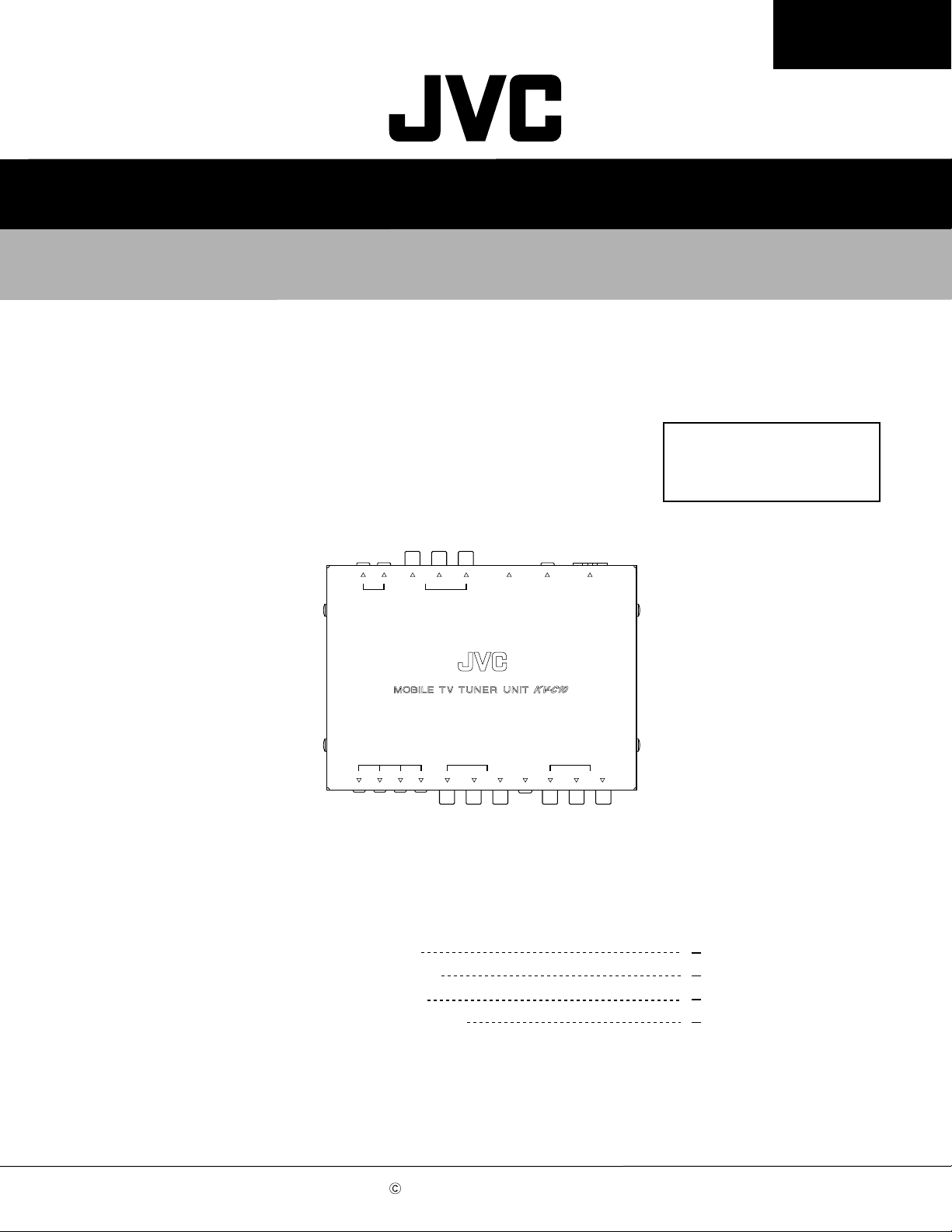
KV-C10
12
HEADPHONE
RL
AUDIO
OUTPUT
ANTENNA INPUT INPUT 2
234
VIDEO L R
Contents
Safety precautions
Disassembly method
Adjustment method
Description of major ICs
VIDEO TO DISPLAY VOCAL POWER
VIDEO
CONTAUDIO L RAUDIOVIDEO1
SUPPLY
INPUT 1
1 2
1 3
1 4
1 6~13
COPYRIGHT 2001 VICTOR COMPANY OF JAPAN, LTD.
No.49654
Aug. 2001
Page 2

KV-C10
Safety precaution
!
Burrs formed during molding may be left over on some parts of the chassis. Therefore,
pay attention to such burrs in the case of preforming repair of this system.
1-2
Page 3
Disassembly method
KV-C10
Removing the metal cover
(See Fig.1)
1.
Remove the four screws A attaching the metal cover
on the back of the body.
2.
Remove the four screws B attaching the metal cover
on both sides of the body.
3.
Remove the metal cover from the body by lifting the
rear part of the cover.
Metal cover
B
A
Fig.1
C
Removing the main board
(See Fig.2 to 3)
Prior to performing the following procedure, remove
the metal cover.
1.
Remove the four screws C attaching the pin jack
and the main board.
2.
Remove the four screws D attaching the main
board.
D
Fig.2
Front panel
Main board
D
Fig.3
1-3
Page 4
KV-C10
Adjustment method
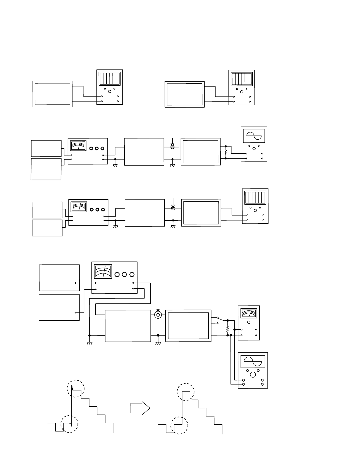
1. Connection
Video
pattern
generator
FM
Signal
generator
Video
pattern
generator
FM
Signal
generator
TP201
GND
Fig. 1
TV Signal generator
TV Signal generator
DC volt meter
+
-
+
-
+
-
Attenuator
Fig. 3
Attenuator
TP202
GND
Antenna receptacle
Video output
Unit under test
Antenna receptacle
Unit under test
GND
TP202
GND
Digital counter
+
-
Fig. 2
Oscilloscope
75 ohm
+
-
DC Volt meter
+
-
Video
pattern
generator
FM
Signal
generator
TV Signal generator
+
-
Attenuator
Fig. 4
Antenna receptacle AC VTVM
L
Audio output
GND
Unit under test
47 kohm
R
+
-
Oscilloscope
+
-
Fig. 5
1-4
Fig. 6
Page 5
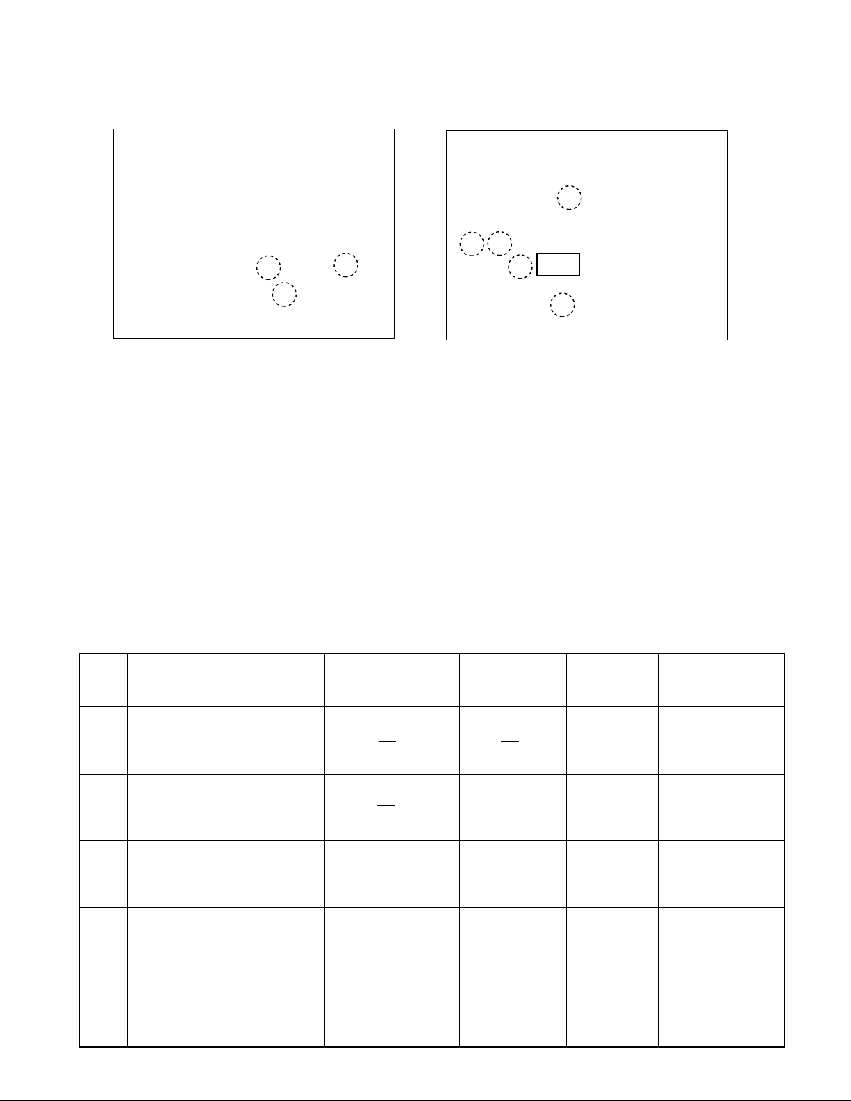
2.
Main board test point location
KV-C10
(Reverse side)
3. Control settings
TP202
H.SYNC
TP201
ANT.LEVEL
TP101
AGC
Fig. 7
VR101
(Foward side)
L103
L101
IC201
VR201
VR202
Power switch ---------------------------------- On
TV channel ------------------------------------ Center position
Video pattern generator -------------------- Color bar
4. Adjust procedures
Step
1
2
3
4
5
Description
Antenna
level
adjustment
H.Sync
adjustment
PIF coil
adjustment
RF AGC
Adjustment
Audio
adjustment
Connection
Fig. 1
Fig. 2
Fig. 3
Fig. 4
Fig. 5
Signal generator
Color bar
Ch 12
60 dBuV
Color bar
Ch 12
60 dBuV
Ch 12
60 dBuV
TV Channel
Ch 12
Ch 12
Ch 12
Test point
TP201
TP202
Video
output
TP101
Audio
output
Adjustment
Adjust VR202
for 1.3V
Adjust VR201
for 15.73kHz
Adjust L101
for see Fig. 6
Adjust VR101
for 3.5V
Adjust L103
for max.output
1-5
Page 6

KV-C10
Description of major ICs
AT24C04AN (IC502) : 2-Wire serial EEPROM
1. Pin layout 2. Pin function
A0
1
A1
2
A2
3
GND
4
3.Block diagram
Vcc
GND
WP
SCL
SDA
A2
A1
A0
8
VCC
7
WP
6
SCL
5
SDA
START
STOP
LOGIC
LOAD
DEVICE
ADDRESS
COMPARATOR
R/W
Pin No.
1~3
4
5
6
7
8
Symbol
A0~A2
GND
SDA
SCL
WP
VCC
SERIAL
CONTROL
LOGIC
COMP
LOAD
INC
DATA WORD
ADDR/COUNTER
Function
Address input
Ground
Serial data
Serial clock
Write protect
VCC
EN
H.V.PUMP/TIMING
DATA RECOVERY
EEPROM
X DEC
Y DEC
D
IN
D
OUT
NJM4052B (IC302) : 4ch / 2ch Analog multiplexer
1.Pin layout
Y0
Y2
Y
Y3
Y1
Inhibit
EE
V
V
SS
1
Yc Y0
2
Y
3
Y3
4
Y1
5
Inhibit
6
7
B A
8
X2
X1
X0
X3
16
15
14
X
13
12
11
10
9
2.Block diagram
V
DD
X2
X1
X
X0
X3
A
B
Inhibit
1-6
A
B
X0
X1
X2
X3
Y0
Y1
Y2
Y3
VSS
Level
control
VDD
VEE
SERIAL MUX
D
OUT
/ACK
LOGIC
Binary to
1-of-4 Decoder
with inhibit
X
Y
Page 7

AN7299 (IC201) : Antenna diversity processor
KV-C10
1. Pin layout
2. Pin function
Pin No.
1
2
3
4
5
6
7
8
9
10
11
12
13
Antenna selection level-hold capacitor
Sync. sepa. video signal input
Horizontal synchronizing signal AFC output
H-sync. setting oscillation time constant setting
H-synchronizing signal output
Composite synchronizing signal output
Vertical synchronizing signal output
GND
V-sync. signal sepa. time constant setting
V-sync. signal oscillation time constant setting
Charge pump integral time-constant setting
VCO oscillation time-constant setting
Antenna selection output 4
1
2
3
4
5
6
7
8
9
10
11
12
Function
24
23
22
21
20
19
18
17
16
15
14
13
Pin No.
14
15
16
17
18
Antenna selection output 3
Antenna selection output 2
Antenna selection output 1
Power supply
Noise comparator level setting
Function
/Antenna fixing
19
20
21
22
23
24
Noise level hold capacitor
Noise comparator input
2nd noise amplifier output
Video clamp input
1st noise amplifier output
Video signal input
3. Block diagram
24
1st
Noise
amp.
separator
1
23
Video
clamp
ANT Choice
Sync
2
22
3
21
2nd
Noise
amp.
Sync
control
Horizontal OSC
4
20
5
19
Noise
comparator
ANT Switch control
separator
Vertical OSC
6
18
V-sync
7
ANT
Select
switch
17
8
16
9
15
ANT Switch driver
ANT Select decoderANT Select control
Phase
detector
Charge
pump
10
14
11
13
1 / 5
Divider
VCO
12
1-7
Page 8

KV-C10
NJM4558M (IC303) : Op. amp.
1.Pin layout
A OUT
A – IN
A + IN
V-
1
2
A
+
–
3
4
B
+
V+
8
B OUT
7
B – IN
6
–
B + IN
5
NJM2246D (IC301) : Video switch
GND
8
6dB
AMP.
Vout
7
V+
6
Vin3
5
Control input - output signal
CTL 1
L
H
L/H
CTL 2
L
L
H
Output
VIN 1
VIN 2
VIN 3
BIAS
1
Vin1
2
CTL1
3
Vin2
4
CTL2
BA6161N (IC102) : Switching Regulator
1. Pin layout
BLOCKING
OSCILLATOR
BA6161N
2. Pin function
Pin No.
Symbol
1
2
DRIVE
3
4
5
GND
FB
N.C.
IN
V
Function
Feed back current return terminal
Transmission drive terminal
Non connection
Power supply input
Ground
1-8
1 2 3 4 5
FB
N.C.
VIN
DRIVE
GND
Page 9

TA1209F (IC101) : TV Converter
1. Pin layout
KV-C10
2. Pin function (1/3)
Pin No.
1
2
Symbol
SD
Output
SD
Trimmer
3
Signal
meter
output
4
Slider
5
6
2nd SIF
Input
2nd SIF
Input
7
8
SIF Vcc
2nd SIF
Output
9
SIF Reg.
output
10
Convertor
Vcc
Video output
(without noise
inverter)
Video output
(with noise
inverter)
Mute SW
Audio output
SIF GND
FM Coil
SIF Regulator
output
Limiter output
Delta filter
Mute output
I/O
O
-
O
-
I
I
-
O
-
Sync.sepa. Input
N.C.
38
39
40
41
42
43
44
45
46
47
48
1
AFT Coil
36 35 34 33 32 31 30 29 28 27 26 25
37
2
3
SD Out
SD Trimmer
Signal meter output
Video Coil
4
Slider
Video Coil
5
Syns,sepa. Output
AFT Coil
TA1209F
7
6
SIF Vcc
2nd SIF Input
2nd SIF Input
Video adjust
PIF Vcc
8
9
2nd SIF Output
SIF Regulator out
ATF Mute
AFT Output
11
10
X'tal
Converter Vcc
RF AGC Delay
RF AGC Output
12
13
X'tal
Converter GND
RF AGC Polarity
24
23
22
21
20
19
18
17
16
15
14
OSC Local
1st PIF AGC Filter
2nd PIF AGC Filter
PIF Input
PIF Input
PIF GND
SIF Input
SIF Input
MIX Output
MIX Output
N.C.
TA1209F
Function
SD Output terminal. (tuned : Hi, not tuned : Lo)
This terminal is open collector output. Connect pull-up register.
Terminal to control SD sensitivity.
Outputted DC voltage rises in proportion to input level.
According to resistance connected between this terminal and GND,
controlling dc offset of #3 terminal is possible.
2nd SIF input terminal. input 2nd SIF output signal through 10.7 MHz ceramic filter.
Built-in matching register for ceramic filter (330 ohm).
Bias terminal for 2nd SIF input. Connect capacitor between this terminal and GND.
SIF Vcc terminal (8.5V is recommended.)
10.7 MHz 2st SIF signal is converted by Lo OSC signal is outputted.
SIF Regulator output terminal (Typ. : 4.8V)
Converter Vcc (8.5V is recommended.)
1-9
Page 10

KV-C10
Pin function (2/3)
Pin No.
11~12
13
Symbol
X'tal
Converter
GND
14
15
16~17
18~19
20
21~22
23
Local OSC
N.C.
MIX Output
SIF Input
PIF GND
PIF Input
2ndPIF
AGC Filter
24
25
26
27
28
29
30
31
32
1nd PIF
AGC Filter
RF AGC
Polarity
RF AGC
Output
RF AGC
Delay
AFT Output
AFT Mute
PIF Vcc
Video
adjust
Sync. sepa.
Output
33
34~35
36
37
AFT Coil
Video coil
AFT Coil
Sync.
sepa.Input
38
39
N.C.
Video
Output
(Without
noise
inverter)
40
Video
Output
(With noise
inverter)
I/O
-
Terminal for connecting crystal resonator to generate local OSC signal.
-
Converter GND
-
Emitter of local circuit. Connect Register and capacitors.
-
Non connection.
O
Mixer output terminal.
I
SIF Input terminal. (input impedance : 1.2 k ohm (Typ.))
-
PIF GND
I
PIF Input terminal. (input impedance : 5 k ohm (Typ.))
-
Terminal to connect capacitor for PIF AGC responsibility, this IC is adopted
Function
dual time constant AGC circuit.
-
Terminal to connect capacitor for PIF AGC responsibility, this IC is adopted
dual time constant AGC circuit.
-
Terminal to switch RF AGC polarity. (open : reverse, GND : forward)
O
RF AGC Output terminal. (open-collector output)
-
Changing comparator reference voltage adjusts RF AGC delay point.
O
AFT Detector output terminal based on double balanced multiplier.
O
AFT Output is muted. when this terminal is connected to GND.
-
PIF Vcc terminal. (5 V is recommended.)
-
Video signal output voltage adjustment terminal. Changing this terminal voltage,
it is possible to adjust video signal output voltage, to 1.0 Vp-p. (With no adjustment,
video signal output voltage is 1 Vp-p(Typ.))
To prevent noise, connecting capacitor (0.01 F) to GND is recommended.
O
Sync, sepa. output terminal.
O
Connect AFT detection coil.
-
Connect video detection coil.
Connect AFT detection coil.
I
Sync, sepa. input terminal.
-
Non connection
O
Video signal output terminal.
Video signal without noise inverter is outputted, and can thus be used for diversity
circuit, for example.
Video output signal voltage is controlled
by voltage of pin 4.
O
Video signal output terminal.
Video signal with noise inverter is outputted,
Video output signal voltage is controlled
by voltage of pin 4.
TA1209F
1-10
Page 11

KV-C10
Pin function (3/3)
Pin No.
41
42
Symbol
Mute SW
Audio
output
43
44
45
46
SIF GND
FM Coil
SIF Reg.
output
Limiter
output
47
48
Delta F
Filter
Mute
output
3. Block diagram
I/O
-
Audio mute SW. (open : mute on, GND : mute off)
O
Audio signal output terminal.
-
SIF GND.
I
Connect FM coil. input limiter output signal through the coil for phase shift.
O
SIF Regulator output terminal. (Typ. : 4.8V)
Function
O
Limiter output terminal.
-
Connect capacitor for delta F circuit.
O
DC voltage in proportion to input level is out putted. this voltage control audio mute.
N.C. Sync. AFT Video Video AFT Sync. Video PIF AFT AFT RF RF RF
sepa. Coil Coil Coil Coil sepa. amp. Vcc Mute Out FAG AGC AGC
input out adjust delay Out Polarity
38 37 36 35 34 33 32 31 30 29 28 27 26 25
TA1209F
TA1209F
Video out
(without
noise
inverter)
Video out
(without
noise
inverter)
Mute switch
Audio out
SIF GND
FM Coil
Regretter
out
Limiter out
DELTA F
39
40
41
42
43
44
45
46
47
V.C.A
SD
FM
detection
Noise
inverter
Delta F
Slider
Sync.
sepa.
Mute
Radio wave
strength
detection
AFT
Limiter
Video
detection
RF AGC
IF AGC
1st Mixer
24
23
22
21
20
19
18
17
16
1st PIF
AGC
Filter
2st PIF
AGC
Filter
PIF Input
PIF Input
PIF GND
SIF Input
SIF Input
MIX Coil
MIX Coil
Mute out
SD
48
trimmer
1 2 3 4 5 6 7 8 9 10 11 12 13 14
SD SD Signal Slider 2nd 2nd SIF 2nd SIF Convert. X'tal Convert. Local
Out Trimmer Meter SIF SIF Vcc SIF Reg. Vcc X'tal GND OSC
Out Input Input Out Out
REG
REG
Local
OSC
15
N.C.
1-11
Page 12

KV-C10
TDA7052B (IC701,IC702) : Mono BTL audio amp. with DC volume control
1. Pin layout
GND1
VC
2. Pin function
1
2 Positive input
3
4 DC volume control
5
6
7
8
V
P
1
2
TDA7052B
TDA7052BT
3
4
SymbolPin No.
V
P
5
OUT -
6
n.c.IN +
7
GND2
8
OUT+
Function
Positive supply voltage
IN+
GND1
Ground
VC
OUT+
n.c.
GND2
OUT -
Positive output
Not connected
Ground
Negative output
3. Block diagram
Positive input
DC volume control
N.C.
7
2
4
TDA7052B
TDA7052B
+
V
ref
V
P
1
STABILIZER
TEMPERATURE
PROTECTION
Signal
ground
5I + i
Positive output 1
8I – i
Negative output 1
6
3
Power
ground
1-12
Page 13

KS5514-09 (IC401) : On screen display processor
1.Pin layout
DGND
SCK
ACB
OSCIN
OSCOUT
CSB
SIN
P1
CLAMPIN
AGND
LPF
AFCFIL
10
11
12
24
1
2
3
4
5
6
7
8
9
23
22
21
20
19
18
17
16
15
14
13
DVDD
P3
P"
XTOUT
XTIN
SYD
AFCR
FSC
AVDD
CVOUT
SCCR
CVIN
2. Block diagram
DVDD P3 P2 XTOUT XTIN SYD AFCR FSC AVDD CVOUT SCCR CVIN
24 23 22 21 20 19 18 17 16 15 14 13
OSD ROM
OSD RAM
DATA
REGISTER
1 2 3 4 5 6 7 8 9 10 11 12
DGND SCK ACB OSCIN OSCOUT CSB SIN P1 CLAMPIN AGND LPF AFCFIL
ADDR
REGISTER
INPUT
CONTROL
DISPLAY
CONTROL
DISPLAY
OSC
4FSC
CONTROL
REGISTER
VSYNC
DET
BLUE BACK
GENERATOR
SHIFT
REGISTER
SYNC
SEP
SYNC
DETECT
VIDEO
MIXER
CLAMP
KV-C10
CLAMP
AFC
INTERNAL
BIAS CKT
3.Pin function
Pin No.
1
2
3
4
5
6
7
8
9
10
11
12
13
14
15
16
17
18
19
20
21
22
23
24
Symbol
DGND
SCK
ACB
OSCIN
OSCOUT
CSB
SIN
P1
CLAMPIN
AGND
LPF
AFCFIL
CVIN
SOCR
CVOUT
AVDD
FSC
AFCR
SYD
XTIN
XTOUT
P2
P3
DVDD
I/O
-
Digital ground
I
Serial clock input. When CSB pin is "L" then serial data is inputted by micom. Hysteresis input.
I
Auto clear pin/ if "L", then all circuit is reset. Built-in pull up resistor. Hysteresis input.
I
LC oscillation pin. Standard frequency is 7MHz & the horizontal start position osc controlled
Function
by the clock of oscillation block.
O
While pin 6 is low, serial data input is active.
I
Built-in pull up resistor.
I
Serial data input port pin. Built-in pull up resistor.
O
General output port 1
I
Clamp input pin of composite video signal.
-
Analog ground.
-
Low pass filter.
-
AFC filter output.
I
Composite video signal input.
I
SECAM chrome input.
O
Composite video output : 2 Vp-p.
-
Analog VDD
I
FSC input (Not use)
I
VCO oscillation frequency control.
O
When sync signal is inputted, then SYD is high.
I
X-TAL
O
X-TAL
O
General output port 2
O
General output port 3
-
Digital VDD
1-13
Page 14

KV-C10
VICTOR COMPANY OF JAPAN, LIMITED
MOBILE ELECTRONICS DIVISION
PERSONAL & MOBILE NETWORK BUSINESS UNIT. 10-1,1Chome,Ohwatari-machi,Maebashi-city,Japan
(No.49654)
200108(V)
 Loading...