

Page 1
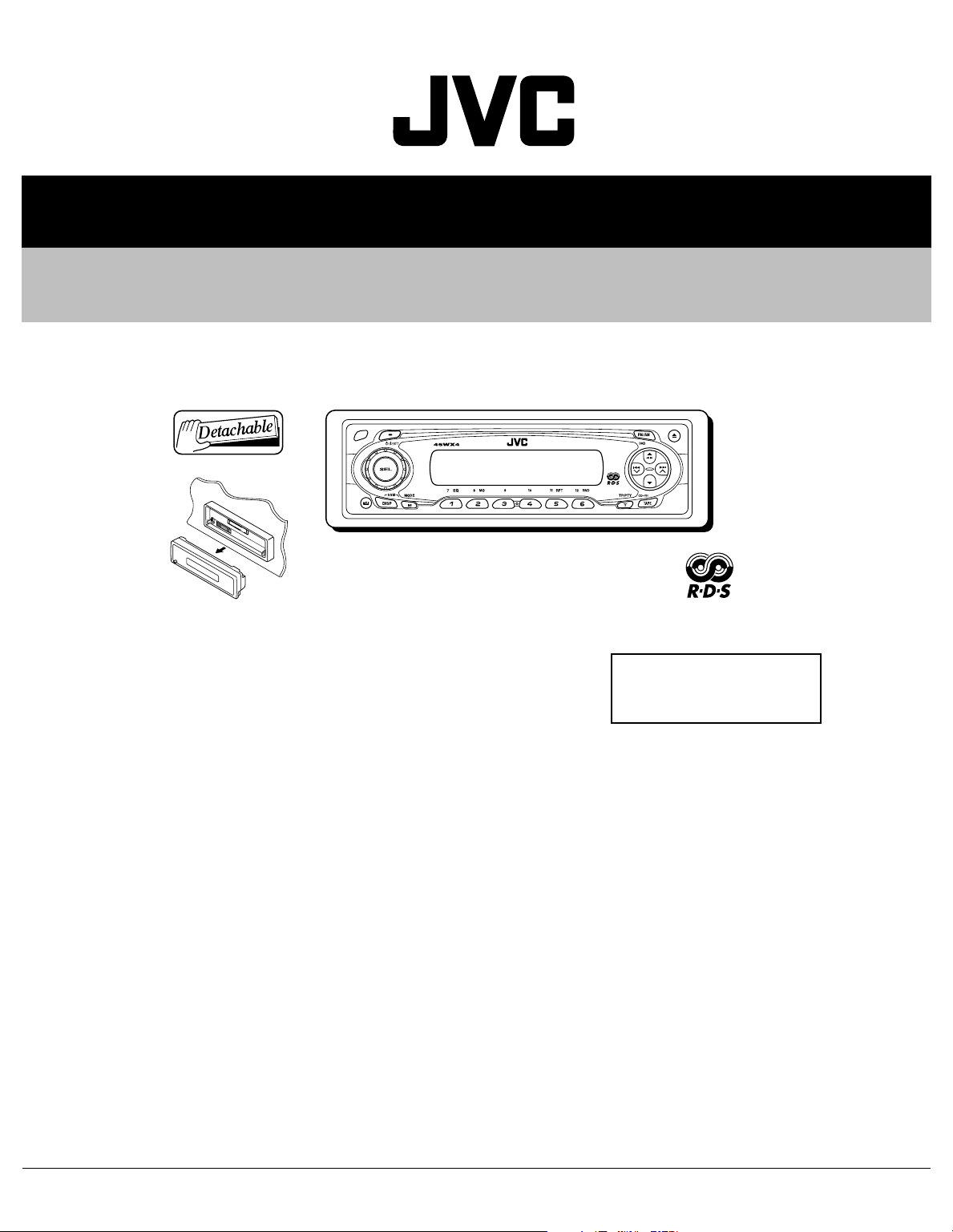
SERVICE MANUAL
CASSETTE RECEIVER
4987320035
KS-FX845R
R
5
84
X
F
-
S
K
Area Suffix
EE --------- Russian Federation
TABLE OF CONTENTS
1 Precautions . . . . . . . . . . . . . . . . . . . . . . . . . . . . . . . . . . . . . . . . . . . . . . . . . . . . . . . . . . . . . . . . . . . . . . . . . . 1-3
2 Disassembly method . . . . . . . . . . . . . . . . . . . . . . . . . . . . . . . . . . . . . . . . . . . . . . . . . . . . . . . . . . . . . . . . . . 1-4
3 Adjustment. . . . . . . . . . . . . . . . . . . . . . . . . . . . . . . . . . . . . . . . . . . . . . . . . . . . . . . . . . . . . . . . . . . . . . . . . . 1-19
4 Description of major ICs. . . . . . . . . . . . . . . . . . . . . . . . . . . . . . . . . . . . . . . . . . . . . . . . . . . . . . . . . . . . . . . 1-23
COPYRIGHT © 2003 VICTOR COMPANY OF JAPAN, LIMITED
No.49873
2003/6
Page 2
SPECIFICATION
AUDIO
AMPLIFIER
SECTION
TUNER SECTION Frequency Range FM1/FM2 87.5 MHz to 108.0 MHz
CASSETTE DECK
SECTION
GENERAL Power Requirement Operating Voltage DC 14.4 V(11 V to 16 V allowance)
Design and specifications are subject to change without notice.
Maximum Power Output Front 45 W per channel
Rear 45 W per channel
Continuous
Power Output
(RMS)
Load
Impedance
Tone Control
Range
Frequency Response 40 Hz to 20 000 Hz
Signal-to-Noise Ratio 70 dB
Line-Out Level/Impedance 2.0 V/20 kΩ load (250 nWb/m)
FM3 65.00 MHz to 74.00 MHz
AM (MW) 522 kHz to 1 620 kHz (LW) 144 kHz to
[FM Tuner] Usable Sensitivity 11.3 dBf (1.0 µV/75 Ω)
[MW Tuner] Sensitivity 20 µV
[LW Tuner] Sensitivity 50 µV
Wow & Flutter 0.11% (WRMS)
Fast-Wind Time 100 sec. (C-60)
Frequency Response 30 Hz to 16 000 Hz(Normal tape)
Signal-to-Noise Ratio 56 dB
Stereo Separation 40 dB
Grounding System Negative ground
Allowable Operating Temperature 0ºC to +40ºC
Dimensions (W × H × D) Installation Size (approx.) 182 mm × 52 mm × 150 mm
Panel Size (approx.) 188 mm × 58 mm × 12 mm
Mass (approx.) 1.5 kg (excluding accessories)
Front 17 W per channel into 4 Ω 40 Hz to 20 000 Hz
at no more than 0.8% total harmonic distortion.
Rear 17 W per channel into 4 Ω 40 Hz to 20 000 Hz
at no more than 0.8% total harmonic distortion.
4 Ω (4 Ω to 8 Ω allowance)
Bass ±10 dB at 100 Hz
Treble ±10 dB at 10 kHz
279 kHz
50 dB Quieting
Sensitivity
Alternate Channel
Selectivity (400 kHz)
Frequency
Response
Stereo Separation 35 dB
Capture Ratio 1.5 dB
Selectivity 35 dB
16.3 dBf (1.8 µV/75 Ω)
65 dB
40 Hz to 15 000 Hz
1-2 (No.49873)
Page 3

1.1 Safety Precautions
SECTION 1
Precautions
!
Burrs formed during molding may be left over on some parts of the chassis. Therefore,
pay attention to such burrs in the case of preforming repair of this system.
(No.49873)1-3
Page 4
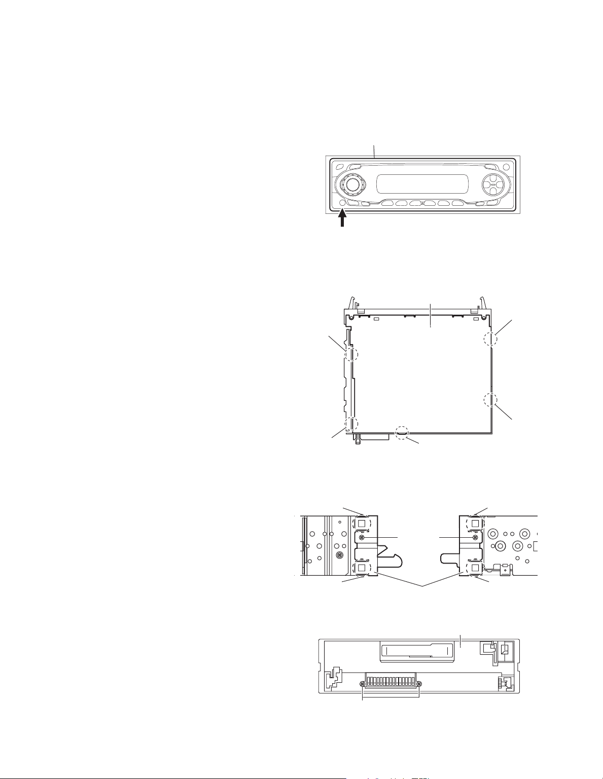
SECTION 2
B
Front chassis assembly
Disassembly method
2.1 Main body
2.1.1 Removing the front panel assembly
(See Fig.1)
• Press the release button and remove the front panel assembly.
2.1.2 Removing the bottom cover
(See Fig.2)
• Prior to performing the following procedures, remove the front
panel assembly.
(1) Turn the main body upside down.
(2) Insert a screwdriver under the joints to release the two
joints a on the left side, two joints b on the right side and
joint c on the back side of the main body, then remove the
bottom cover from the main body.
CAUTION:
When releasing the joints using a screwd rive r, do no t damage
the main board.
Front panel assembly
Release button
Fig.1
Bottom cover
Joint b
Joint a
2.1.3 Removing the front chassis assembly
(See Figs.3 and 4)
• Prior to performing the following procedures, remove the front
panel assembly and bottom cover.
(1) Remove the two screws A on the both sides of the main
body. (See Fig.3.)
(2) Remove the two screws B on the front side of the main
body. (See Fig.4.)
(3) Release the two joints d and two joints e on the both sides
of the main body, then remove the front chassis assembly
toward the front. (See Fig.3.)
Joint a
Joint d
Joint d
Joint c
Fig.3
A
Front chassis assembly
A
Fig.3
Joint b
Joint e
Joint e
1-4 (No.49873)
Fig.4
Page 5
2.1.4 Removing the heat sink
(See Fig.5)
• Prior to performing the following procedure, remove the front
panel assembly.
(1) R emove the two screws C and screw D attaching the heat
sink on the left side of the main body, and remove the heat
sink.
C
2.1.5 Removing the rear panel
(See Fig.6)
• Prior to performing the following procedure, remove the front
panel assembly and bottom cover.
(1) Remove the two screws E, three screws F and three
screws G attaching the rear panel on the back side of the
main body.
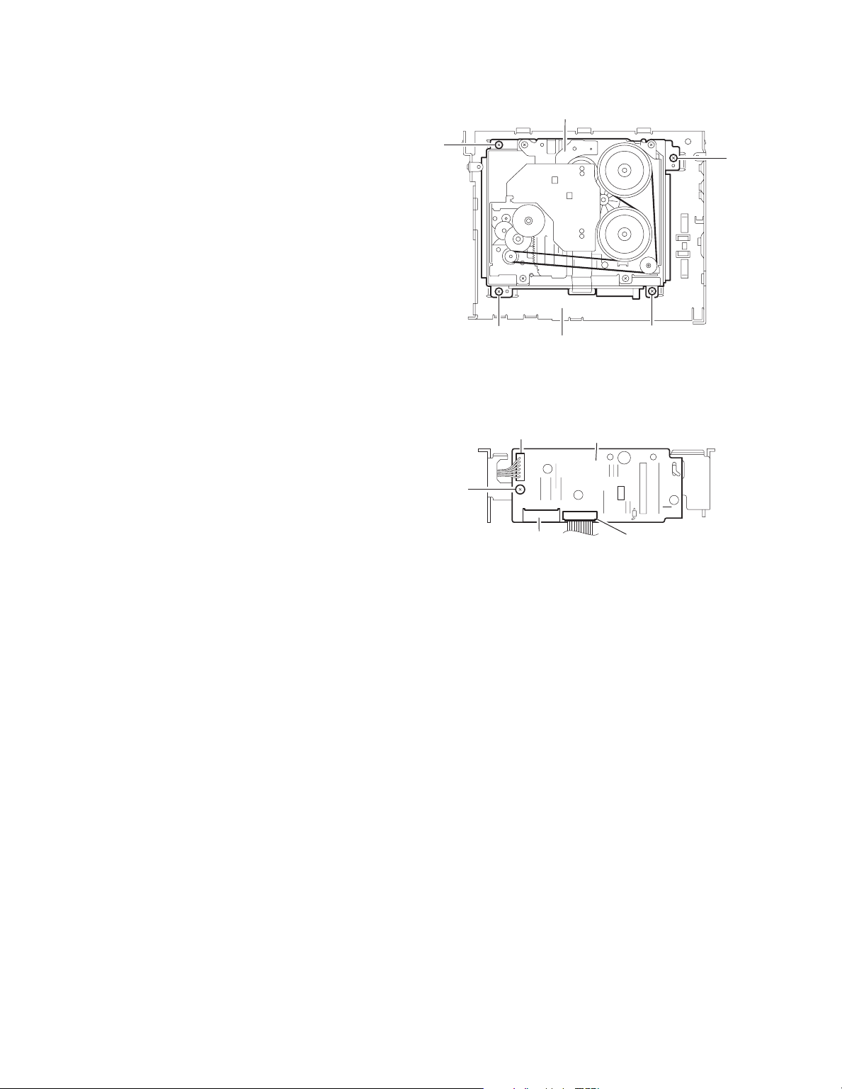
2.1.6 Removing the main board
(See Fig.7)
• Prior to performing the following procedures, remove the front
panel assembly, bottom cover, front chassis assembly, heat
sink and rear panel.
(1) Remove the two screws H attaching the main board on the
top chassis.
(2) D isconnect the connector CP401 on the main board from
the cassette mechanism assembly.
E
D
Rear bracket
Heat sink
Fig.5
Fig.6
G
F
G
E
H
Main board
H
CP701
Fig.7
(No.49873)1-5
Page 6
2.1.7 Removing the cassette mechanism assembly
(See Fig.8)
• Prior to performing the following procedures, remove the front
panel assembly, bottom cover, front chassis assembly, heat
sink, rear panel and main board.
(1) Disconnect the wire from the connector CN402 on the
mecha board.
(2) Disconnect the card wire from the connector CN403 on the
mecha board.
(3) Remove the four screws J attaching the cassette mecha-
nism assembly to the top chassis, take out the cassette
mechanism assembly.
Cassette mechanism assembly
H
H
2.1.8 Removing the mecha board
(See Fig.9)
• Prior to performing the following procedures, remove the front
panel assembly, bottom cover, front chassis assembly, heat
sink, rear panel and main board.
(1) Disconnect the wire from the connector CN402 on the
mecha board.
(2) Disconnect the card wire from the connector CN403 on the
mecha board.
(3) Remove the screw K attaching the mecha board.
(4) Bend the hook f in the direction of the arrow 1 and move the
mecha board in the direction of the arrow 2.
(5) Remove the mecha board from the mecha bracket (L) of
the top chassis.
H H
CN402
Top chassis
Fig.8
Mecha board
J
CN401
Fig.9
CN403
1-6 (No.49873)
Page 7
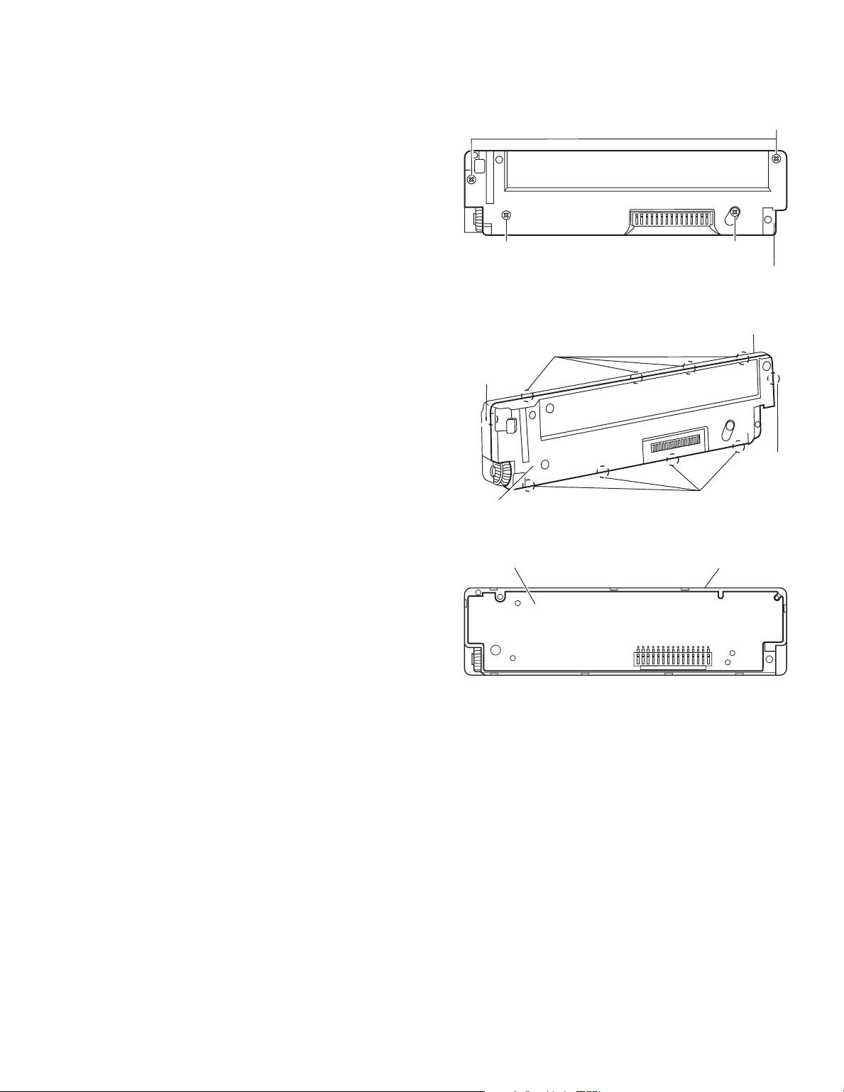
2.1.9 Removing the front board
(See Figs.10 to 12)
• Prior to performing the following procedures, remove the front
panel assembly.
(1) Remove the four screws L attaching the rear cover on the
back side of the front panel assembly. (See Fig.10.)
(2) Release the ten joints g, the front panel assembly and rear
cover become separate. (See Fig.11.)
(3) Remove the front board from the front panel assembly.
(See Fig.12.)
L
L
Joint g
Rear cover
Front board
Joints
L
Rear cover
Fig.10
Front panel assembly
g
Joint g
Joints g
Fig.11
Front panel assembly
Fig.12
(No.49873)1-7
Page 8
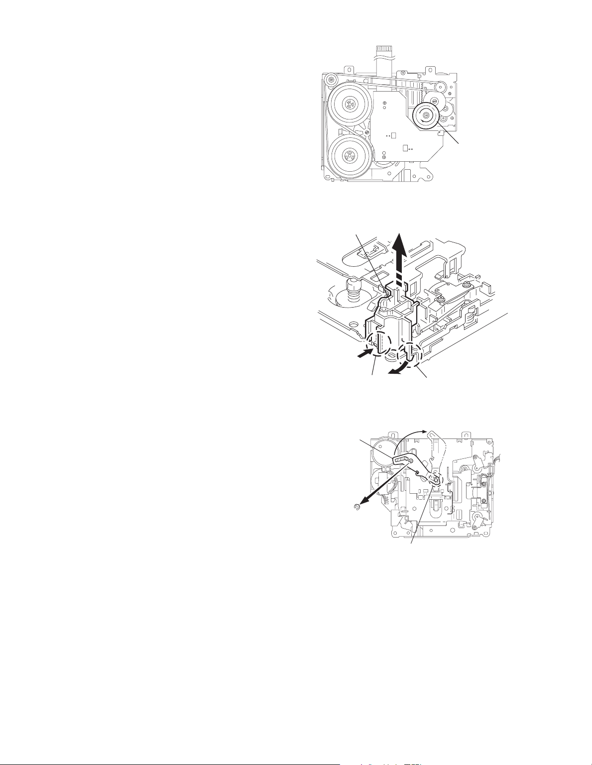
2.2 Cassette mechanism assembly
r
REFERENCE:
Prior to performing the following procedures, turn the mode
gear on the bottom of the body until the respective part comes
to the EJECT position (Refer to Fig.1).
2.2.1 Removing the cassette guide
(See Fig.2)
(1) Turn the mode gear to set to RVS play or subsequent
mode.
(2) Remove the cassette guide from the main chassis while re-
leasing each two joint tabs a in the direction of the arrow.
Mode gea
Fig.1
Cassette guide
2.2.2 Removing the load arm
(See Fig.3)
(1) Remove the E-washer attaching the load arm.
(2) Move the load arm in the direction of the arrow and release
the joint b on the cassette catch.
Load arm
E-washer
Tab a
Tab a
Fig.2
Joint b
Fig.3
1-8 (No.49873)
Page 9
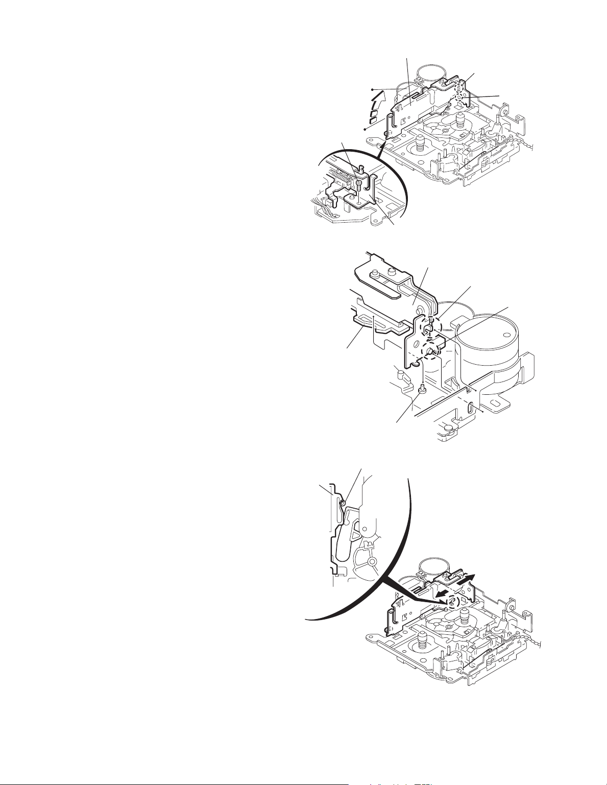
2.2.3 Removing the cassette hanger assembly / cassette holder
r
(See Fig.4 to 7)
(1) Check the mode is set to EJECT. Push down the front part
of the cassette holder and move in the direction of the arrow to release the joint c.
(2) Move the rear part of the cassette hanger assembly in the
direction of the arrow to release it from the two joint bosses
d.
(3) Release the holder stabilizer spring from the hooks e and
f, then pull out from the cassette hanger assembly.
(4) Bring up the rear side of the cassette hanger assembly to
release the joint g and h.
(5) Pull out the cassette catch from the cassette hanger as-
sembly.
Cassette holder assembly
Side bracket
Joints c
Cassette holder assembly
Fig.4
Boss d
Cassette hanger
assembly
Boss d
Cassette stabilizer spring
Hook e
Cassette holder
assembly
Hook g
Cassette hange
assembly
Hook f
Fig.5
Cassette hanger
assembly
Hook h
Fig.6
Cassette hanger assembly
Cassette catch
Cassette holder assembly
Fig.7
(No.49873)1-9
Page 10
2.2.4 Removing the side bracket assembly
(See Fig.8 to 10)
(1) Remove the screw A attaching the side bracket assembly.
(2) Detach the front side of the side bracket assembly upward
and pull out forward to release the joint i and j in the rear.
CAUTION:
When reassembling, make sure that the boss k of the
main chassis is set in the notch of the load rack under the
side bracket assembly. Do not reattach the load rack on
the boss k.
CAUTION:
After reattaching the side bracket assembly, confirm operation.
Side bracket assembly
Joint i
Joint j
A
Side bracket assembly
Fig.8
Side bracket assembly
Joint i
Joint j
Load rack
Load rack
Boss k
Fig.9
Boss k
1-10 (No.49873)
Fig.10
Page 11
2.2.5 Removing the pinch arm (F) assembly
r
(See Fig.11 and 12)
(1) Remove the polywasher and pull out the pinch arm (F) as-
sembly.
(2) Remove the compulsion spring.
2.2.6 Removing the pinch arm (R) assembly
(See Fig.11 and 12)
(1) Remove the polywasher and pull out the pinch arm (R) as-
sembly.
2.2.7 Removing the slide chassis assembly
(See Fig.13 and 14)
REFERENCE:
It is not necessary to remove the head and the tape guide.
(1) Move the slide chassis assembly in the direction of the ar-
row to release the two joints l and remove from the main
chassis.
(2) Remove the rack link.
CAUTION:
When reassembling, first reatta ch the ra ck link, an d next
fit the boss m and hook n of the slide chassis assembly
to the hole of the main chassis, and engage the two joints
l.
Joint l
Joint l
Slide chassis assembly
Fig.13
Head
Tape guide
Boss m
Rack link
Hook n
Polywasher
Polywasher
Compulsion
spring
Pinch arm
(R) assembly
Pinch arm
(F) assembly
Fig.11
Pinch arm (F) assembly
Pinch arm
(R) assembly
Polywashe
Fig.14
Polywasher
Fig.12
(No.49873)1-11
Page 12

2.2.8 Removing the head / tape guide
(See Fig.16 and 17)
REFERENCE:
It is not necessary to remove the slide chassis assembly.
(1) Remove the band attaching the wire to the head.
(2) Remove the two screws B, the head and the head support
spring.
(3) Remove the pinch arm spring from the tape guide.
(4) Remove the tape guide and the pinch spring arm.
CAUTION:
When reattaching the pinch arm spring, set both end of
it to the pinch spring arm (remarked o).
CAUTION:
When reattaching the head, set the wires into the groove
of the tape guide (Fig.16).
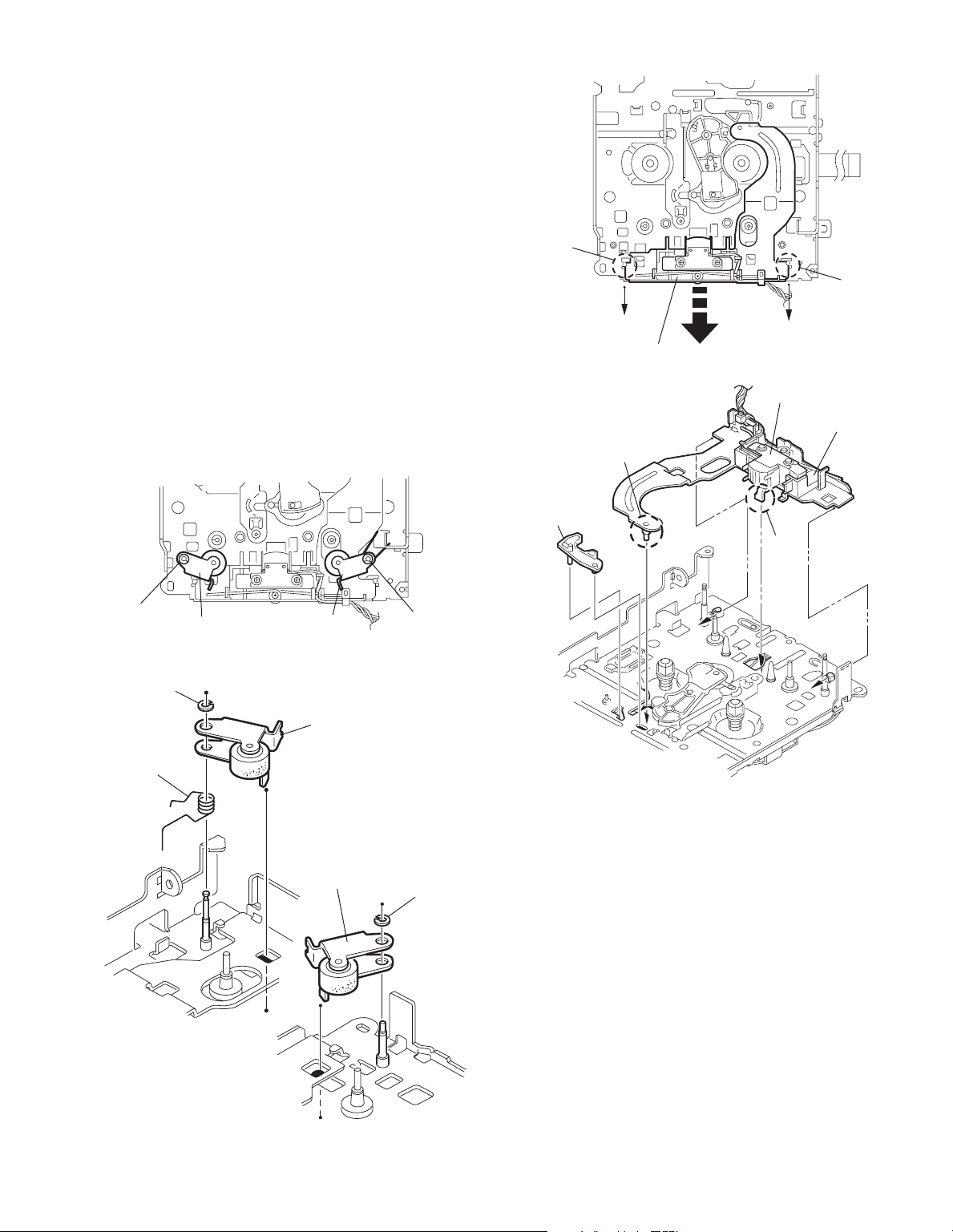
2.2.9 Removing the flywheel assembly (F) & (R)
(See Fig.18 and 19)
REFERENCE:
It is not necessary to remove the slide chassis assembly.
(1) Remove the belt at the bottom.
(2) Remove the two polywashers on the upper side.
(3) Pull out each flywheel assembly downward.
B
Slide chassis assembly
Flywheel assembly (F)
Flywheel assembly (R)
Belt
Fig.17
Polywasher
Polywasher
Head
Head support spring
Tape guide
Pinch spring arm
Head
Fig.15
o
Tape guide
B
Pinch arm spring
Flywheel assembly (F)
Flywheel assembly (R)
Fig.18
o
1-12 (No.49873)
Slid chassis assembly
Fig.16
Page 13

2.2.10 Disassembling the flywheel assembly (F)
r
(See Fig.19 and 20)
(1) Push and turn counterclockwise the spring holder (F) to re-
lease the three joints p on the bottom of the flywheel.
(2) T he spring holder (F), the TU spring and the friction gear
play come off.
(3) Remove the polywasher and felt.
2.2.11 Disassembling the flywheel assembly (R)
(See Fig.19 and 20)
(1) Push and turn clockwise the spring holder (R) to release
the three joints q on the bottom of the flywheel.
(2) T he spring holder (R), the FF spring and the friction gear
FF come off.
(3) Remove the polywasher and the felt.
2.2.12 Removing the reel board
(See Fig.21 and 22)
(1) R emove the two screws C attaching the reel board.
(2) Move the reel board in the direction of the arrow to release
the joint r.
(3) Unsolder the wires if necessary.
CAUTION:
When reattaching, confirm operation of the MODE
switch and the ST-BY switch.The mode position between EJECT and ST-BY is optimum for reattaching.Connect the card wire extending from the reel board
to the FFC pad before reattaching the reel board.
FFC pad
C
Joint
Reel board
C
Fig.21
FFC pad
CT-1 switch
MODE switch
Flywheel
assembly (F)
Joint p
Joints p
Fig.19
Polywasher
Spring holder (R)
Spring holder (F)
TU spring
Friction gear FF
Friction gear play
Polywasher
FF spring
Flywheel
assembly (R)
Joints q
Joint q
Soldering
ST-BY switch
Fig.22
Felt
Flywheel assembly (F)
Fig.20
Felt
Flywheel assembly (R)
(No.49873)1-13
Page 14

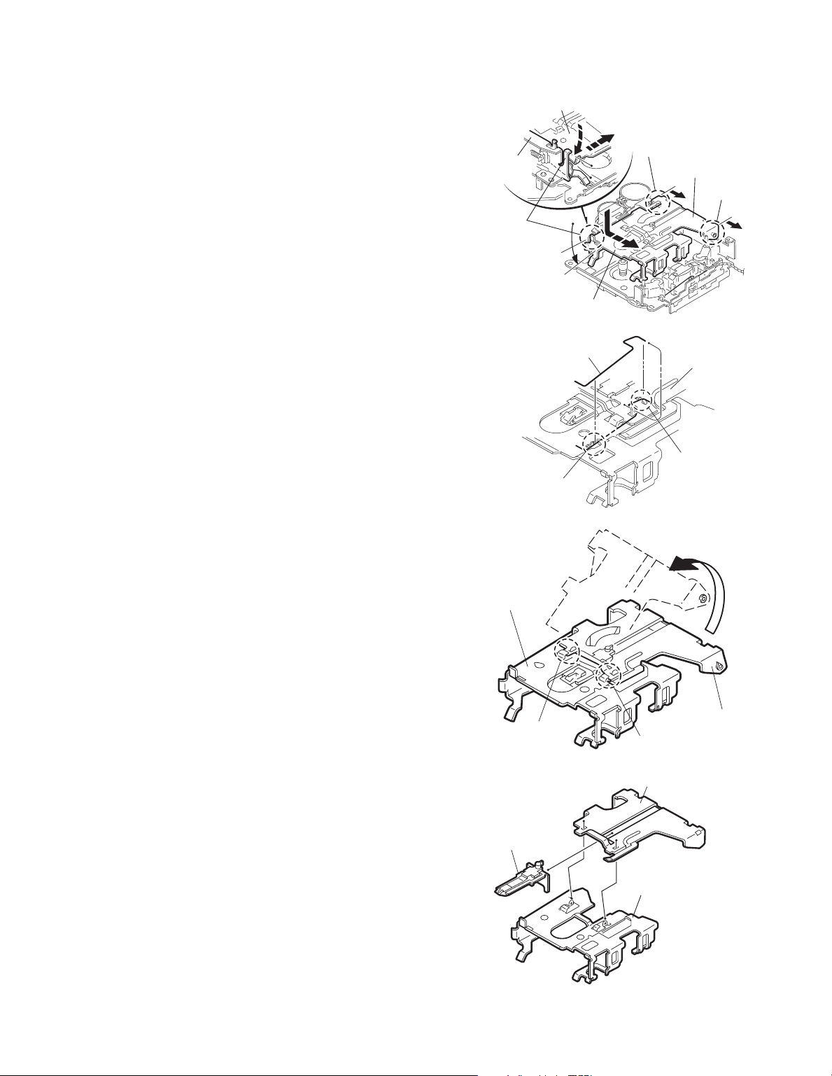
2.2.13 Removing the gear base arm / gear base link assembly
(See Fig.23 to 25)
(1) Move the gear base arm in the direction of the arrow.
(2) Insert a slotted screwdriver to the gear base spring under
the gear base arm, and release the gear base arm upward
from the boss on the gear base assembly.
(3) Remove the gear base arm from the main chassis while re-
leasing the two joints s.
(4) Move the gear base link assemby in the direction of the ar-
row to release the two joints t.
REFERENCE:
When reattaching the gear base arm, make sure that the
boss on the gear base assembly is inside the gear base
spring.
2.2.14 Removing the FFC pad
(See Fig.25 and 27)
(1) Push each joint hook u of the FFC pad and remove toward
the bottom.
Gear base
link assembly
Gear base spring
Joint t
Gear base arm
Joints s
Hook u
FFC pad
Hook u
Joint t
Fig.23
Gear base arm
Screwdriver
Gear base link
assembly
Fig.24
Gear base arm
FFC pad
Fig.25
1-14 (No.49873)
Page 15

2.2.15 Removing the mode gear
r
r
(See Fig.26 and 29)
(1) Remove the polywasher on the bottom and pull out the
mode gear.
2.2.16 Removing the mode switch actuator
(See Fig.26, 27 and 29)
(1) Pull out the mode switch actuator at the bottom.
REFERENCE:
When reattaching the mode switch actuator to the main
chassis, make sure to set on the shaft and insert v into
the slot w.
2.2.17 Removing the direction link / direction plate
(See Fig.27 to 29)
(1) Remove the polywasher attaching the direction link.
(2) B ring up the direction link to release the three joints x, y
and z at a time.
(3) Move the direction plate in the direction of the arrow to re-
lease the two joints a’.
REFERENCE:
When reattaching the direction plate, engage the two
joints a’ and move in the direction of the arrow (Refer to
Fig.28).
REFERENCE:
When reattaching the direction link, move the direction
plate in the direction of the arrow and engage the three
joint x, y and z at a time (Refer to Fig.29).
2.2.18 Removing the mode rack assembly
(See Fig.27 and 28)
(1) Move the mode rack assembly in the direction of the arrow
to release the two joints b’ and the joint c’.
REFERENCE:
When reattaching, set the two b’ on the bottom of the
mode rack assembly into the slots of the main chassis
and move in the direction of the arrow (See Fig.28).
Direction plate
Direction plate
Joints a'
Joint z
Direction link
Direction plate
Mode switch actuator
Direction link
Fig.26
Slot w
Joint y
Polywasher
Fig.27
Mode rack assembly
Joint b'
Mode gear
Polywashe
Mode rack assembly
Joint x
Joint b'
Joint c'
Joints a'
Fig.28
Direction link
Mode switch actuator
Polywasher
v
Mode gea
Direction plate
Mode rack assembly
Fig.29
(No.49873)1-15
Page 16

2.2.19 Removing the gear base assembly / take up gear / reflector gear
r
(See Fig.30 to 32)
(1) Push in the pin d’ of the gear base assembly on the upper
side of the body and move the reflector gear toward the
bottom, then pull out.
(2) Remove the polywasher on the bottom and pull out the
take up gear.
(3) Move the gear base assembly in the direction of the arrow
to release it from the two slots e’ of the main chassis.
REFERENCE:
The parts are damaged when removed. Please replace
with new ones.
2.2.20 Removing the reel driver / reel spindle
(See Fig.32)
(1) Draw out the reel driver from the shaft on the main chassis
and remove the reel driver spring and the reel spindle respectively.
CAUTION:
The reel driver is damaged when removed. Please replace with a new one.
Gear base assembly
Pin d'
Polywasher
Slot e'
Slot e'
Fig.30
Take up gear
Reflector gear
Reel driver
Reel driver spring
Reel spindle
Main chassis
Reflector gear
Fig.31
Reel driver
Reel driver spring
Reel spindle
Gear base assembly
Slots e’
Take up gea
Polywasher
Fig.32
1-16 (No.49873)
Page 17

2.2.21 Removing the side bracket assembly
(See Fig.33 to 37)
(1) Remove the eject cam plate spring.
(2) Push the joint f’ through the slot to remove the load rack
downward.
(3) Move the eject cam limiter in the direction of the arrow to
release it from the boss g’ of the side bracket assembly and
from the two joints h’.
(4) Move the eject cam plate in the direction of the arrow to re-
lease the joint i’.
CAUTION:
When reassembling, confirm operation of each part before reattaching the eject cam plate spring.
Joint f'
Side bracket assembly
Boss g'
Eject cam plate
Fig.36
Side bracket assembly
Joint i'
Eject cam plate spring
Side bracket assembly
Joint h'
Side bracket
assembly
Boss g'
Boss g'
Load rack
Fig.33
Eject cam limiter
Joint f'
Fig.34
Eject cam limiter
Eject cam plate
Joint i'
Fig.37
Joint h'
Load rack
Joint h'
Eject cam plate
Fig.35
Joint h'
(No.49873)1-17
Page 18

2.2.22 Removing the main motor assembly / sub motor assembly
r
r
r
(See Fig.38 to 40)
(1) Remove the belt at the bottom.
(2) Remove the polywasher and pull out the mode gear.
(3) Pull out the reduction gear (B).
(4) Remove the polywasher and pull out the reduction gear
(A).
(5) Remove the two screws attaching the main motor assem-
bly.
(6) Remove the two screws E attaching the sub motor assem-
bly.
(7) Unsolder the wires on the reel board if necessary.
CAUTION:
When reassembling, adjust the length of the wires extending from the sub motor asswmbly by attaching them
to the side of the sub motor assembly with the wires extending from the main motor assembly using a spacer.
Belt
Reduction gear (B)
Reduction gear (B)
E
Mode gear
Polywasher
Fig.38
Main motor
D
assembly
Reduction
gear (A)
Polywashe
Sub moto
assembly
E
Polywasher
Reduction gear (A)
D
Spacer
Sub motor assembly
Fig.39
Main motor assembly
Sub motor assembly
Fig.40
Main motor assembly
Space
1-18 (No.49873)
Page 19

SECTION 3
Adjustment
3.1 Adjustment method Test instruments required for adjustment
(1) Digital oscilloscope (100MHz)
(2) Frequency counter meter
(3) Electric voltmeter
(4) Wow & flutter meter
(5) Test tapes
• VT724...........................For DOLBY level measurement
• VT739..............For playback frequency measurement
• VT712....For wow flutter & tape speed measurement
• VT703........................For head azimuth measurement
(6) Torque gauge............................Cassette type for CTG-N
Measuring conditions (Amplifier section)
• Power supply voltage.............. DC14.4V (11V to 16V allowance)
• Load impedance............ 4Ω (4Ω to 8Ω allowance)
• Line out level/Impedance..............1.0V/20k load (250 nWb/m)
Standard volume position
Balance and Bass, Treble volume, Fader : Center (Indication "0")
Loudness, Dolby NR, Sound, Cruise : Off
Volume position is about 2V at speaker output with following
conditions, Playback the test tape VT721.
AM mode 999kHz/62dB, INT/400Hz, 30%
modulation signal on receiving.
FM mono mode 97.9MHz/66dB, INT/400Hz, 22.5kHz
deviation pilot off mono
FM stereo mode 1kHz, 67.5kHz dev. pilot 7.5kHz dev.
Output level 0dB (1µV,50Ω/open terminal)
(No.49873)1-19
Page 20

Information for using a car audio service jig
(1) We're advancing efforts to make our extension cords common for all car audio products.
Please use this type of extension cord as follows.
(2) As a U-shape type top cover is employed, this type of extension cord is needed to check operation of the mechanism assembly
after disassembly.
(3) Extension cord : EXTKSRT002-18P ( 18 pin extension cord ) For connection between mechanism assemblyand main board.
(4) Check for mechanism drivin g section such as motor ,etc.
Disassembly method
(1) Remove the front panel assembly.
(2) Remove the bottom cover.
(3) Remove the front chassis.
(4) Remove the heat sink.
(5) Remove the rear panel
(6) Remove the main board.
(7) Reattach the heat sink with the two screws B. (Refer to Disassembly method.)
(8) Reattach the rear panel with the screw E. (Refer to Disassembly method.)
(9) Reattach the front panel assembly.
(10) Confirm that current is being carried by connecting an extension cord jig.
NOTE:
Available to connect to the CJ601
CAUTION :
Be sure to attach the heat sink and rear panel on the power amplifier IC and regulator IC of a main board when supplying
the power.If voltage is applied without attaching those parts, the power amplifier IC and regulator IC will be destroyed
by heat.
connector when installing the front panel.
To
Cassette mechanism
EXTKSRT002-18P
Extension cord
EXTKSRT002-18P
To
Main board
Front panel assembly
Cassette mechanism
Main board
1-20 (No.49873)
Page 21

Arrangement of adjusting & test points
A
Cassette mechanism
(Surface)
Motor assembly
Tape speed adjust
Azimuth screw
(Forward)
Playback head
Azimuth screw B
(Reverse)
Head section view
Azimuth screw B
(Reverse)
Playback head
Azimuth screw A
(Forward)
(No.49873)1-21
Page 22

Item Conditions Adjustment and Confirmation methods S.Values Adjust
1. Head azimuth adjustment
Test tape:
SCC-1659
VT703 (10kHz)
Head height adjustment
Adjust the azimuth directly. When you adjust the height
using a mirror tape, remove the cassette housing from
the mechanism chassis. After installing the cassette
housing, perform the azimuth adjustment.
(1) Load the SCC-1659 mirror tape. Adjust with height
adjustment screw A and azimuth adjustment screw
B so that line A of the mirror tape runs in the center
between Lch and Rch in the reverse play mode.
(2) After switching from REV to FWD then to REV,
check that the head position set in procedure 1 is not
changed. (If the position has shifted, adjust again
and check.)
(3) Adjust with azimuth adjustment screw B so that line
B of the mirror tape runs in the center between Lch
and Rch in the forward play mode.
Head shield
The head is at low position
during.
Head shield
The head is at High position
during REV.
A line
B line
Test tape:
VT724 (1kHz)
VT703 (10kHz)
VT721 (315Hz)
2. Tape speed
and wow flutter confirmation
3. Play back
frequency response confirmation
The tuner section is of an adjustment-freedesign. In case the tuner is in trouble, replace the tuner pack.
Test tape:
VT712 (3kHz)
Test tape:
VT724 (1kHz)
VT739 (63Hz /
1kHz / 10kHz)
Head azimuth adjustment
(1) Load VT724 (1kHz) and play it back in the reverse
play mode. Set the Rch output level to max.
(2) Load VT703 (10kHz) and play it back in the forward
play mode. Adjust the Rch and Lch output levels to
max, with azimuth adjustment screw B. In this case,
the phase difference should be within 45 .
(3) Engage the reverse mode and adjust the output lev-
el to max, with azimuth adjustment screw C.(The
phase difference should be 45 or more.)
(4) When switching between forward and reverse
modes, the difference between channels should be
within 3dB. (Between FWD L and R, REV L and R.)
(5) When VT721 (315Hz) is played back, the level differ-
ence between channels should be within 1.5dB.
(1) Check to see if the reading of the F, counter / wow
flutter meter is within 3015Hz to 3045Hz (FWD/
REV), and less than 0.35% (JIS RMS).
(2) In case of out of specification, adjust the motor with
a built-in volume resistor.
(1) Play test tape VT724, and set the volume position at
2V.
(2) Play test tape VT739 and confirm.1kHz / 10kHz: -1
±3dB,1kHz / 63Hz: 0 ±3dB,
(3) When 10kHz is out of specification, it will be neces-
sary to read adjust the azimuth.
Output
level:
Maximum
FWD Adj B
REV Adj C
Tape speed:
3015Hz to 3045Hz
Wow flutter:
less than 0.35%
Speaker out
1kHz / 63Hz: 0 ±3dB
1kHz / 10kHz: -1 ±3dB
PBHead
HEIGHT Adj A
(0 ) (45 )
phase
Built-in volume
resistor
1-22 (No.49873)
Page 23

4.1 HA13164A (IC901) : Regulator
• Terminal layout
123456789101112131415
• Block diagram
ANT OUT
EXT OUT
ANT CTRL
CTRL
CD OUT
AUDIO OUT
C3
0.1u
C4
0.1u
C5
0.1u
C6
10u
2
1
7
11
12
10
SECTION 4
Description of major ICs
C1
100u
VCC ACC
8
Surge Protector
BIAS TSD
3
15
TAB
ILM AJGND GND
C2
0.1u
13
+B
ACC
BATT.DET OUT
9
COMPOUT
6
VDD OUT
4
SW5VOUT
5
ILMOUT
14
R1
C7
0.1u
0.1u
C8
UNIT R:
C:F
note1) TAB (header of IC)
connected to GND
• Pin function
Pin No. Symbol Function
1 EXTOUT Output voltage is VCC-1 V when M or H level applied to CTRL pin.
2 ANTOUT Output voltage is VCC-1 V when M or H level to CTRL pin and H level to ANT-CTRL.
3 ACCIN Connected to ACC.
4 VDDOUT Regular 5.7V.
5 SW5VOUT Output voltage is 5V when M or H level applied to CTRL pin.
6 COMPOUT Output for ACC detector.
7 ANT CTRL L:ANT output OFF H:ANT output ON
8 VCC Connected to VCC.
9 BATT DET Low battery detect.
10 AUDIO OUT Output voltage is 9V when M or H level applied to CTRL pin.
11 CTRL L:BIAS OFF M:BIAS ON H:CD ON
12 CD OUT Output voltage is 8V when H level applied to CTRL pin.
13 ILM AJ Adjustment pin for ILM output voltage.
14 ILM OUT Output voltage is 10V when M or H level applied to CTRL pin.
15 GND Connected to GND.
(No.49873)1-23
Page 24

4.2 LC75823W (IC601) : LCD driver
• Pin Layout
DICLCE
OSC
Vss
VDD2
VDD1
INH
VDD
COM3
COM2
COM1
S52
S51
S50
S49
64 63 62 61 60 59 58 57 56 55 54 53 52 51 50 49
1
S1
S2
S3
S4
S5
S6
S7
S8
S9
S10
S11
S12
S13
S14
S15
S16
2
3
4
5
6
7
8
9
10
11
12
13
14
15
16
48
47
46
45
44
43
42
41
40
39
38
37
36
35
34
33
S48
S47
S46
S45
S44
S43
S42
S41
S40
S39
S38
S37
S36
S35
S34
S33
17 18 19 20 21 22 23 24 25 26 27 28 29 30 31 32
S17
S18
S19
S20
S21
S22
S23
S24
S25
S26
S27
S28
S29
S30
S31
S32
• Pin function
Pin No. Symbol I/O Functions
1 to 52 S1 to S52 O Segment output pins used to display data transferred by serial data input.
53 to 55 COM1 to COM3 O Common driver output pins. The frame frequency is given by : t0=(fosc/384)Hz.
56 VDD -- Power supply connection. Provide a voltage of between 4.5 and 6.0V.
57 INH
58 VDD1 I Used for applying the LCD drive 2/3 bias voltage externally.
59 VDD2 I Used for applying the LCD drive 1/3 bias voltage externally.
60 Vss -- Power supply connection. Connect to GND.
61 OSC I/O Oscillator connection.
62 CE I Serial data interface connection to the controller. CE : Chip enable
63 CL I Serial data interface connection to the controller. CL : Sync clock
64 DI I Serial data interface connection to the controller. DI : Transfer data
I Display turning off input pin.
="L" (Vss) ----- off (S1 to S52, COM1 to COM3="L"
INT
="H" (VDD)----- on
INT
Serial data can be transferred in display off mode.
Must be connected to VDD2 when a 1/2 bias drive scheme is used.
Must be connected to VDD1 when a 1/2 bias drive scheme is used.
An oscillator circuit is formed by connecting an external resistor and capacitor at this pin.
1-24 (No.49873)
Page 25

4.3 SAA6579T-X (IC71):RDS detecter
• Pin layout
QUAL
DATA
Vref
MUX
GND
CIN
SCOUT
1
2
3
4
dd
V
5
6
7
8
16
15
14
13
12
11
10
9
• Block diagram
CLK
T57
OSCO
OSCI
V
dd
GND
TEST
MODE
121413
4
8
7
CLOCKED
COMPARATOR
5
3
REFERENCE
VOLTAGE
ANTIALIASING
FILTER
6 11
VP1
57 kHz
BAND PASS
(8th ORDER)
COSTAS LOOP
VARIABLE AND
FIXED DIVIDER
CLOCK
REGERATION
AND SYNC
• Pin function
Pin No. Symbol Description
1 QUAL Quality indicatio n output
2 DATA RDS data output
3 Vref Reference voltage output (0.5VDDA)
4 MUX Multiolex signal input
5 Vdd +5V supply voltage for analog part
6 GND Ground for analog part (0V)
7 CIN Sub carrier input to comparator
8 SCOUT Sub carrier output of reconstruction filter
9 MODE Oscillator mode / test control input
10 TEST Test enable input
11 GND Ground for digital part (0V)
12 Vdd +5V supply voltage for digital part
13 OSCI Oscillator input
14 OSCO Oscillator output
15 T57 57 kHz clock signal output
16 CLK RDS clock output
RECONSTRUCTION
FILTER
TEST LOGIC AND OUTPUT
SELECTOR SWITCH
OSCILLATOR
AND
DIVIDER
BIPHASE
SYMBOL
DECODER
910
QUALITY BIT
GENERATOR
DIFFERENTIAL
DECODER
1
2
15
15
(No.49873)1-25
Page 26

4.4 TB2118F-X (IC31) : PLL
• Terminal Layout
2423222120191817161514
13
• Block diagram
FM VCO
AMVCO
DIN
DOUT
123456789
osc
2
1
XO
24
XI
15
16
IFC
13
CE
3
4
CK
5
6
Buff.
ON/OFF
OSC circuit
AMP
AMP
AMP
Serial
Interface
0112
Reference Counter
Prescaler
20-bit BINARY COUNTER
Resistor 1
Resistor 2
I/O PORT
Phase
Comparator
4-bit
Swallow counter
12-bit
Programmable counter
22-bit
40bit shift register
OUTPUT PORT
Constant
power supply voltage
switch
Vdd
switch
Vcc
AM CP.
20
+
+
-
RF
22
19
Vt
18
FM cp
7
SL
8
9
I/O -2I/O -1
10 11
12
out-2out-1
vdd2
14
17
21
23
a-gnd
vccd-gndvdd
• Pin Function
Pin
Symbol I/O Function
No.
Pin
Symbol I/O Function
No.
1 XOUT O Crystal oscillator pin 13 IFC I IF signal input
2 OSC - Non connect 14 VDD - Power pins for digital block
3 CE I Chip enable input 15 FMIN I FM band local signal input
4 DI I Serial data input 16 AMIN I AM band local signal input
5 CK I Clock input 17 DGND - Connect to GND (for digital circuit)
6 DOUT O Serial data output 18 FMCP O Charge pump output for FM
7 SR O Register control pin 19 Vt - Tuning voltage biased to 2.5V.
8 I/01 I/O I/O ports 20 AMCP O Charge pump output for AM
9 I/02 I/O I/O ports 21 VCC - Power pins for analog block
10 OUT1 - Non connect 22 RF I Ripple filter connecting pin
11 OUT2 - Non connect 23 AGND - Connect to GND (for analog circuit)
12 VDD2 - Single power supply for REF. frequency block 24 XIN I Crystal oscillator pin
1-26 (No.49873)
Page 27

4.5 TEA6320T-X (IC161) : E.volume
• Pin layout
SDA
1
GND
2
OUTLR
3
OUTLF
4
TL
5
B2L
6
B1L
7
IVL
8
ILL
9
QSL
10
IDL
11
MUTE
12
ICL
13
IBL
IAL
14
15
16
CD-CH
TAP E
TUNER
IMD
• Block diagram
10 8 9 7 6
32
31
30
29
28
27
26
25
24
23
22
21
20
19
18
17
SCL
VCC
OUTRR
OUTRF
TR
B2R
B1R
IVR
ILR
QSR
IDR
Vref
ICR
CAP
IBR
IAR
5
12
21
31
19
POWER
SUPPLY
2
VOLUME 1
+20 to -31 dB
LOUDNESS
LEFT
16
15
13
11
22
20
14
SOURCE
SELECTOR
VOLUME 1
+20 to -31 dB
LOUDNESS
RIGHT
18
17
23 25 24 26 27 28
• Pin functions
Pin
No.
Symbol I/O Functions
1 SDA I/O Serial data input/output.
2 GND - Ground.
3 OUTLR O output left rear.
4 OUTLF O output left front.
5 TL I Treble control capacitor left channel
or input from an external equalizer.
6 B2L - Bass control capacitor left channel or
output to an external equalizer.
7 B1L - Bass control capacitor left channel.
8 IVL I Input volume 1. left contro l part.
9 ILL I Input loudness. left control part.
10 QSL O Output source selector. left channel.
11 IDL - Not used
12 MUTE - Not used
13 ICL I Input C left source.
14 IMO - Not used
15 IBL I Input B left source.
16 IAL I Input A left source.
BASS
LEFT
+15 dB
LOGIC
BASS
RIGHT
+15 dB
VOLUME 2
0 to 55 dB
BALANCE
FENDER REAR
VOLUME 2
0 to 55 dB
BALANCE
FENDER FRONT
HC BUS
REC
VOLUME 2
0 to -55dB
BALANCE
FENDER FRONT
VOLUME 2
0 to -55dB
BALANCE
FENDER REAR
3
4
32
1
29
30
TREBLE
LEFT
+12 dB
TREBLE
RIGHT
+12 dB
Pin
No.
MUTE
FUNCTION
ZERO CROSS
DETECTOR
Symbol I/O Functions
17 IAR I Input A right source.
18 IBR I Input B right source.
19 CAP - Electronic filtering for supply.
20 ICR I Input C right source.
21 Vref - Reference voltage (0.5Vcc)
22 IDR - Not used
23 QSR O Output source selector right channel.
24 ILR I Input loudness right channel.
25 IVR I Input volume 1. right control part.
26 B1R - Bass control capacitor right channel
27 B2R O Bass control capacitor right channel
or output to an external equalizer.
28 TR I Treble control capacitor right channel
or input from an external equalizer.
29 OUTRF O Output right front.
30 OUTRR O Output right rear.
31 Vcc - Supply voltage.
32 SCL I Serial clock input.
(No.49873)1-27
Page 28

4.6 UPD784215AGC226 (IC701) : Main micon
• Pin layout & Block diagram
100
1
76
75
25
26
• Pin function
Pin No. Symbol I/O Function
1 TAPE IN I Cassette tape inside signal H:Inside L:Outside
2 STAND BY I Stand-by position detection signal input H:Loading L:Eject side
3 to 8 no use - Not used
9 VDD Micon power supply
10 X2
11 X1
12 VSS GND
13 XT2
14 XT1
15 RESET I System reset
16 Steering I Steering remocon input
17 BUS-INT I J-BUS INT
18 PS2 I Power save2 H means STOP mode
19 no use - Not used
20 RDS-SCK I RDS clock input
21 RDS DA I RDS data input
22 REMOCON I Remocon input
23 AVDD A/D converter power supply
24 AVREF0 A/D reference voltage
25 VOL,1 I Volume encoder pulse input 1
26 VOL,2 I Volume encoder pulse input 2
27 KEY0 I Key input 0
28 KEY1 I Key input 1
29 KEY2 I Key input 2
30 LEVEL I Level meter input
31 SQ I S.Quality level input
32 SM I S.METER input
33 AVSS GND
34,35 no use - Not used
36 AVREF
37 BUS-SI I J-BUS data input
38 BUS-SO O J-BUS data output
39 BUS-SCK I/O J-BUS clock input/output
40 BUS-I/O O J-BUS selection output;Hinput L
41 LCD-DA O Data output for LCD driver
42 LCD-SCK O CLK output for LCD driver
43 LCD-CE O CE for LCD driver
44 no use - Not used
45 E2PROM-DI I I2C data input
46 E2PROM-DO O I2C data output
47 E2PROM-CLK O I2C clock output
48 OPEN I DOOR OPEN SW
49,50 no use - Not used
50
51
1-28 (No.49873)
Page 29

Pin No. Symbol I/O Function
51,52 no use - Not used
53 SD/ST I Station detector or streo indicator input ;
H means a station is there. L means the program is stereo.
54 no use - Not used
55 MONO O Monaural selection output ; H means monaural
56 to 60 no use - Not used
61 DETACH I Detach detect input ; H means detaching
62 AFCK O A check outpu
63 SEEK/STOP O Auto seek and stop selecting output ;
H means seeking L means receiving.
64 IF CONT O IF control output
65 FM/AM O FM AM band selecting output ; H = FML= AM
66 PAL-CUE O CUE output for PAL ICE
67 PAL-DO O Data output for PAL ICE
68 PAL-CLK O Clock output for PAL ICE
69 PAL-DI I Data input from PAL ICE
70 TEL-MUTING I Telephone muting detection input ;
Active level can be selected H or L in PSM
71 no use - Not used
72 VSS GND
73 no use - Not used
74 PS1 I Power Save1 L= ACC off
75 POWER O Power ON/OFF control output H=power on
76 no use - Not used
77 MUTING O Muting output L=muting on
78 to 80 no use - Not used
81 VDD Micon power supply
82 no use - Not used
83 VOL-DA O Data output for e-vol ICE
84 VOL-CLK O Clock output for e-vol ICE
85 to 89 no use - Not used
90 STAGE1 I Feature selection (refer to tabel1)
91 MOTOR O Main motor control H:Motor drive
92 FF/REW O Audio level control for MS H:Play mode L:FF/REW mode
93 HEAD SEL(F/R) O Audio signal selector for head amp H:REV L:FWD
94 TEST For rewriting flash memory
95 DOLBY O Dolby ON/OFF control H:Dolby on
96 MS IN I MS signal input L:no music
97 REEL I Reel pulse signal input (Pulse signal)
98 SUBMO- O Sub motor control. Eject direction
99 SUBMO+ O Sub motor control. Loading direction
100 MODE I Mecha position detection signal
(No.49873)1-29
Page 30

4.7 BR24L16F-W-X (IC771) : EEPROM
A
• Pin layout • Pin function
VCC WP SCL SDA
Symbol I/O Function
VCC - Power supply.
GND - GND
A0,A1,A2 I No use connect to GND.
SCL I Serial clock inp u t.
SDA I/O Serial data I/O of slave and ward address.
A0 A1 A2 GND
WP I Write protect terminal.
• Block diagram
A0 1
11bit
A1 2
A2 3
GND 4
High voltage osc circuit
Address
decoder
11bit
START
Control circuit
4.8 RPM6938-SV4 (IC602) : Remote control receiver
• Pin diagram
1 2 3
• Block diagram
16kbit EEPROM allay
Slave Ward
Address resister
STOP
Power supply
voltage det.
ACK
8bit
Data
resister
8 Vcc
7 WP
6 SCL
5 SD
1-30 (No.49873)
I/V
conversion
AMP
PD
magnetic shield
BPF
fo
trimming
circuit
AGC
Detector
Vcc
Comp
Vcc
22k
Rout
GND
Page 31

4.9 HA12231FP-X (IC401) : PB Equalizer/Line Mute/Music Sensor
• Pin layout & Block diagram
Vcc
14 13 12 11 10
8
9
Ripple Filter
ALC
1 2 3 4 5 6
GND
Amp.
Ch2
Amp.
Ch1
7
• Pin function
Pin No. Symbol I/O Function
1 VREF O Reference output
2 FIN(R) I Equalizer input
3 RIN(R) I Equalizer input
4 EQOUT(R) O Equalizer output
5 TAI(R) I Tape input
6 PBOUT(R) O PB output
7 MS GV - MS gain terminal
8 120/70 I Mode control input
9 Mute I Mode control input
10 FOR/REV I Mode control input
11 Vcc - Power supply
12 MS O MS output (to MPU)
13 MSDET - Time constant pin for MS rectifier
14 RIP - Ripple filter
15 PBOUT(L) O PB output
16 TAI(L) I Tape input
17 EQOUT(L) O Equalizer output
18 RIN(L) I Equalizer input
19 FIN(L) I Equalizer input
20 GND - Ground
(No.49873)1-31
Page 32

4.10 LA4743K (IC301) : Power amp.
• Block diagram
IN 1
TAB
IN 2
+
0.22 F
+
0.22 F
11
1
12
Vcc 1/2 Vcc 3/4
6 20
-
+
Protective
circuit
-
+
2200 F 0.022 F
+
9
7
+
OUT 1+
OUT 1-
PWR GND1
8
+
OUT 2+
5
-
OUT 2-
3
PWR GND2
2
ST BY
R.F
47 F
IN 3
PRE GND
IN 4
+5V
ST ON
+
0.22 F
N.C
+
0.22 F
4
Stand by
Switch
Mute
3.3 F
OUT 3+
OUT 3-
10K
+
Low Level
Mute ON
10
+
Ripple
Filter
Mute
circuit
22
+
15
-
+
-
17
19
25
18
21
23
PWR GND3
OUT 4+
OUT 4-
13
14
Protective
circuit
-
+
+
-
ON TIME C
1-32 (No.49873)
22 F
Muting &
16
+
ON Time Control
Circuit
PWR GND4
24
Page 33

• Pin layout
TAB
GND
FR-
STDBY
FR+
VP1
RR-
GND
RR+
RIPPLE
INRF
INRR
SGND
FLIN
RLIN
DNTIME
RL+
GND
RL-
VP3
FL+
MUTE
FL-
GND
NC
• Pin function
Pin No. Symbol Function Pin No. Symbol Function
1 TAB Header of IC 14 FLIN Front Lch input
2 GND Power GND 15 RLIN Rear Lch input
3 FR- Outpur(-) for front Rch 16 ONTIME Power on time control
4 STDBY Stand by input 17 RL+ Output (+) for rear Lch
5 FR+ Output (+) for front Rch 18 GND Power GND
6 VP1 Power input 19 RL- Output (-) for rear Lch
7 RR- Output (-) for rear Rch 20 VP3 Power input
8 GND Power GND 21 FL+ Output (+) for front
9 RR+ Output (+) for rear Rch 22 MUTE Muting control input
10 RIPPLE Ripple filter 23 FL- Output (-) for front
11 RRIN Rear Rch input 24 GND Power GND
12 FRIN Front Rch input 25 NC Non connection
13 SGND Signal GND
4.11 IC-PST600M/G/-W (IC702) : System reset
Co1
OP1
4.12 LB1641 (IC402) : DC Motor driver
• Pin layout • Truth table
Input Output Mode
IN1 IN2 OUT1 OUT2
0000 Brake
1 2 3 4 5 6 7 8 9
GND OUT1 P1
VZ IN1 IN2
VCC1
VCC2 P2
10
OUT2
1010 CLOCKWISE
0101COUNTER-CLOCKWISE
1100 Brake
1
3
2
IN
Vout
GND
(No.49873)1-33
Page 34

4.13 HD74HC126FP-X (IC801) : Buffer
• Pin layout • Pin function
Input Output
CA Y
LX Z
HL H
HH L
Note:
H:High level
L:Low level
X:Irrelevant
Z:Off(High-impedance)
State a 3-state input
• Block diagram
1C
1A
1Y
2C
2A
2Y
GND
1
2
3
4
5
6
7
14
13
12
11
10
9
8
VCC
4C
4A
4Y
3C
3A
3Y
Vcc Vcc
1k
Input
Note:
CL includes probe and jig capacitance
See Function Table
1A
2A
3A
4A
1C
2C
3C
4C
1Y
2Y
3Y
4Y
Output
Output
Output
Output
S1
CL
1k
Sample as Load Circuit 1
Sample as Load Circuit 1
Sample as Load Circuit 1
1-34 (No.49873)
Page 35

(No.49873)1-35
Page 36

VICTOR COMPANY OF JAPAN, LIMITED
AV & MULTIMEDIA COMPANY MOBILE ENTERTAINMENT CATEGORY 10-1,1chome,Ohwatari-machi,Maebashi-city,371-8543,Japan
(No.49873)
Printed in Japan
WPC
 Loading...