

Page 1
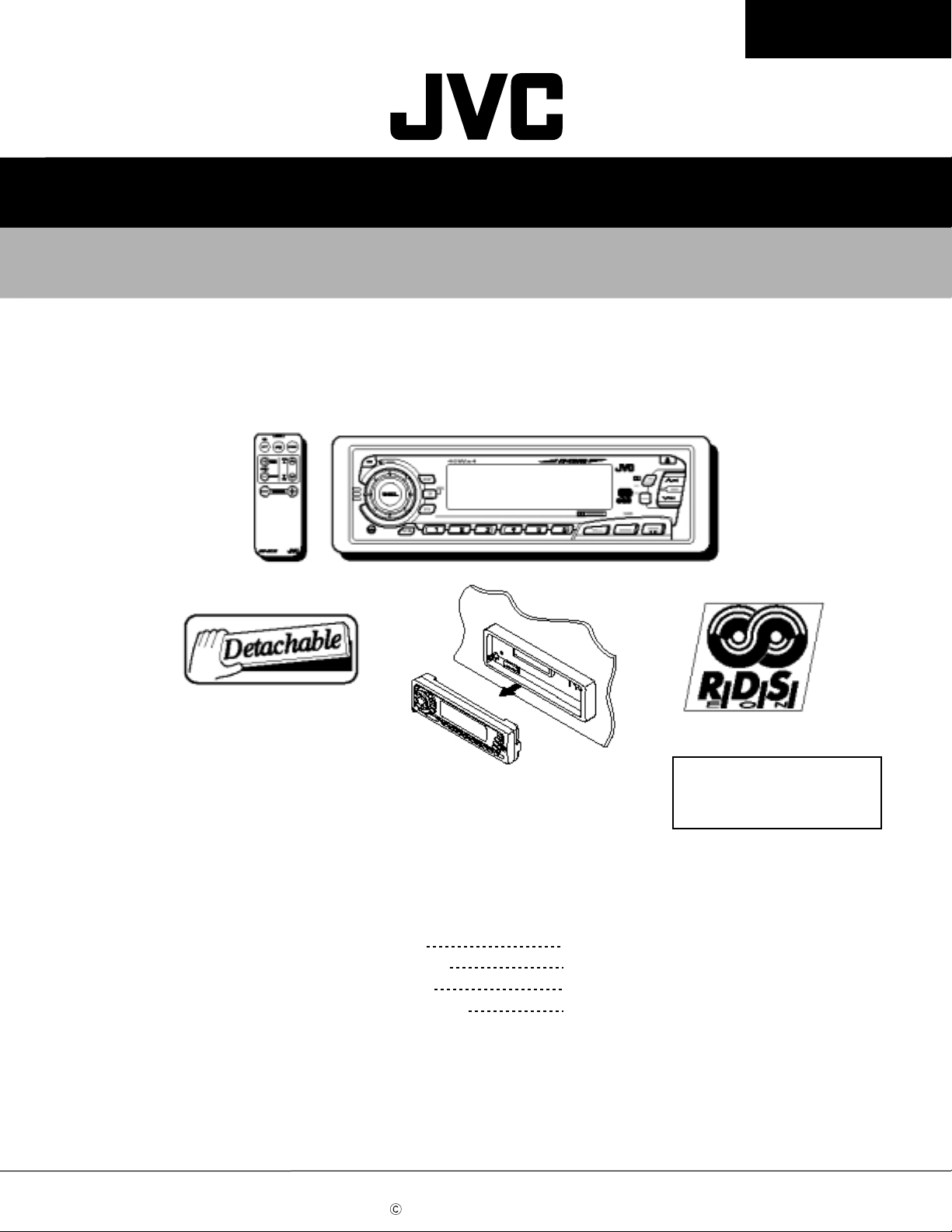
SERVICE MANUAL
CASSETTE RECEIVER
KS-FX834R
KS-FX834R
Contents
Safety precaution
Disassembly method
Adjustment method
Description of major ICs
This service manual is printed on 100% recycled paper.
COPYRIGHT 2000 VICTOR COMPANY OF JAPAN, LTD.
Area Suffix
E ---- Continental Europe
1-2
1-3
1-10
1-14
No.49571
Sep. 2000
Page 2

KS-FX834R
Safety precaution
CAUTION
!
Burrs formed during molding may be left over on some parts of the chassis. Therefore,
pay attention to such burrs in the case of preforming repair of this system.
1-2
Page 3
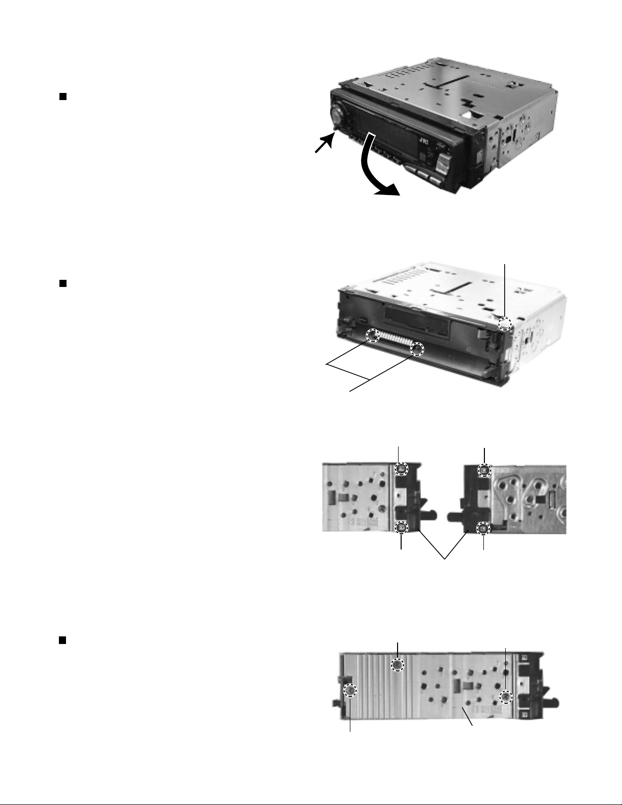
Disassembly method
Removing the front panel unit
(See Fig.1)
1. Press the release switch and remove the front
panel unit in the direction of the arrow.
KS-FX834R
Fig.1
c
Removing the front chassis
1.2.Remove the two screws A attaching the front
chassis.
Insert a screwdriver to the two joints a on the side
of the front chassis, two joints b on the right side
and one joint c from upside, then detach the front
chassis toward the front side.
(See Fig.2~3)
A
a
a
Front chassis
Fig.2
b
b
Removing the heat sink
1. Remove the three screws B attaching the heat sink
on the left side of the body, and remove the heat
sink.
(See Fig.4)
B
B
Fig. 3
B
Heat sink
Fig. 4
1-3
Page 4
KS-FX834R
Removing the bottom cover
1.2.Turn the body upside down.
Insert a screwdriver to the two joints d and two
joints e on both sides of the body and the joint f on
the back of the body, then detach the bottom cover
from the body.
Removing the rear panel
1.
Remove the front chassis.
(See Fig.5)
(See Fig.6 )
Bottom cover
d
e
f
Fig. 5
C
2.
Remove the heat sink.
3.
Remove the bottom cover.
4.
Remove the five screws B attaching the rear panel
and one screw C attaching the pine jack on the
back of the body.
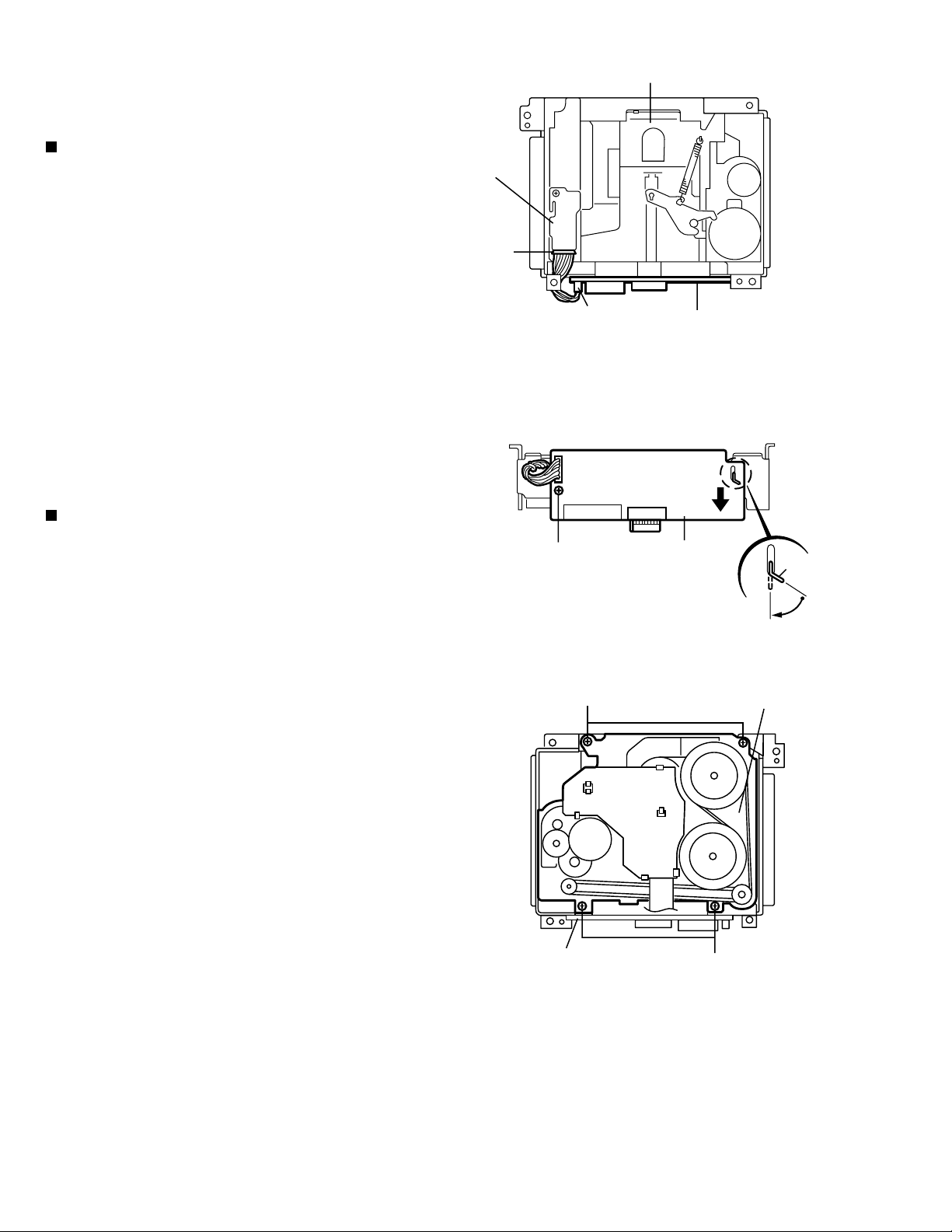
Removing the main amplifier board
assembly
1.
Remove the front chassis.
2.
Remove the bottom cover.
3.
Remove the rear panel.
4.
Remove the two screws D attaching the main
amplifier board assembly on the top cover.
5.
Disconnect connector CP701 on the main amplifier
board assembly from the cassette mechanism
assembly.
(See Fig.7)
B
D
B
B
Fig. 6
Main board assembly
D
CP701
Fig. 7
1-4
Page 5
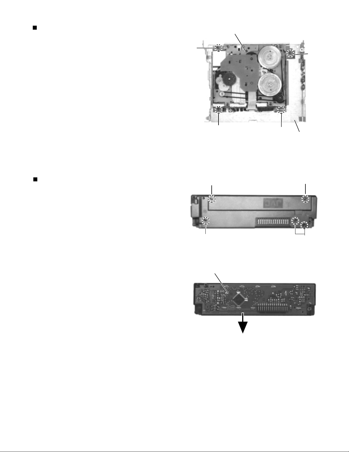
KS-FX834R
Removing the Cassette mechanism
assembly
1.
Remove the front chassis.
2.
Remove the bottom cover.
3.
Remove the main amplifier board assembly.
4.
Remove the fore screws F attaching the cassette
mechanism assembly from the top cover.
(See Fig.8)
Removing the control switch board
(See Fig.9 and 10 )
Cassette mechanism assembly
F
F
Fig. 8
G
F
Top cover
F
G
1.
Remove the front panel unit from the main body.
2.
Remove the five screws G attaching the rear cover
on the back of the front panel unit.
3.
Remove the control switch board from the front
panel unit.
G
Fig. 9
LCD & Key control board
Fig. 10
G
1-5
Page 6
KS-FX834R
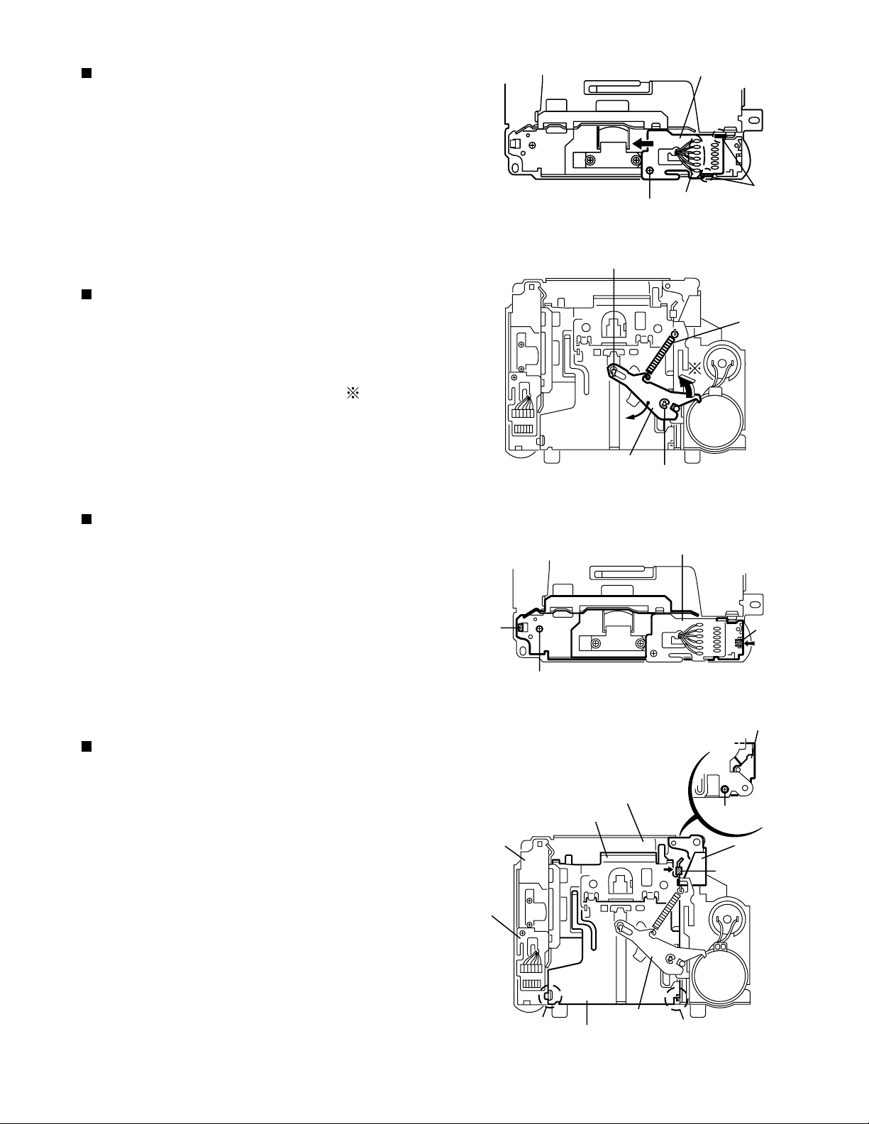
<Removal of the cassette mechanism>
Cassette mechanism ass’y
Removing the mecha control P.W.B.
(See Fig.1 and 2)
1.
For the 6pin harness extending from connector
CN402 on the mecha control P.W.B, disconnect it
from the head relay P.W.B.
2.
Disconnect the card wire from connector CN403 on
the mecha control P.W.B.
3.
Remove the screw A attaching the mecha control
P. W. B .
4.
Move the tab a as shown in Fig.2 and remove the
mecha control P.W.B. while moving it in the direction
of the arrow.
Removing the cassette mechanism
assembly (See Fig.1 to 3)
1.
Disconnect the 6pin harness from connector CN402
and the card wire from CN403 on the mecha control
P.W.B. (Refer to Fig.1 and 2).
Head relay
P.W.B.
6pin
harness
CN402
CN402
Mecha control
A
CN403
Fig.1
CN403
Fig.2
Mecha control
P.W.B.
P.W.B.
Tab a
2.
Remove the four screws B on the bottom of the
cassette mechanism.
Mecha control
B
P.W.B.
Cassette mechanism ass’y
B
Fig.3
1-6
Page 7
KS-FX834R
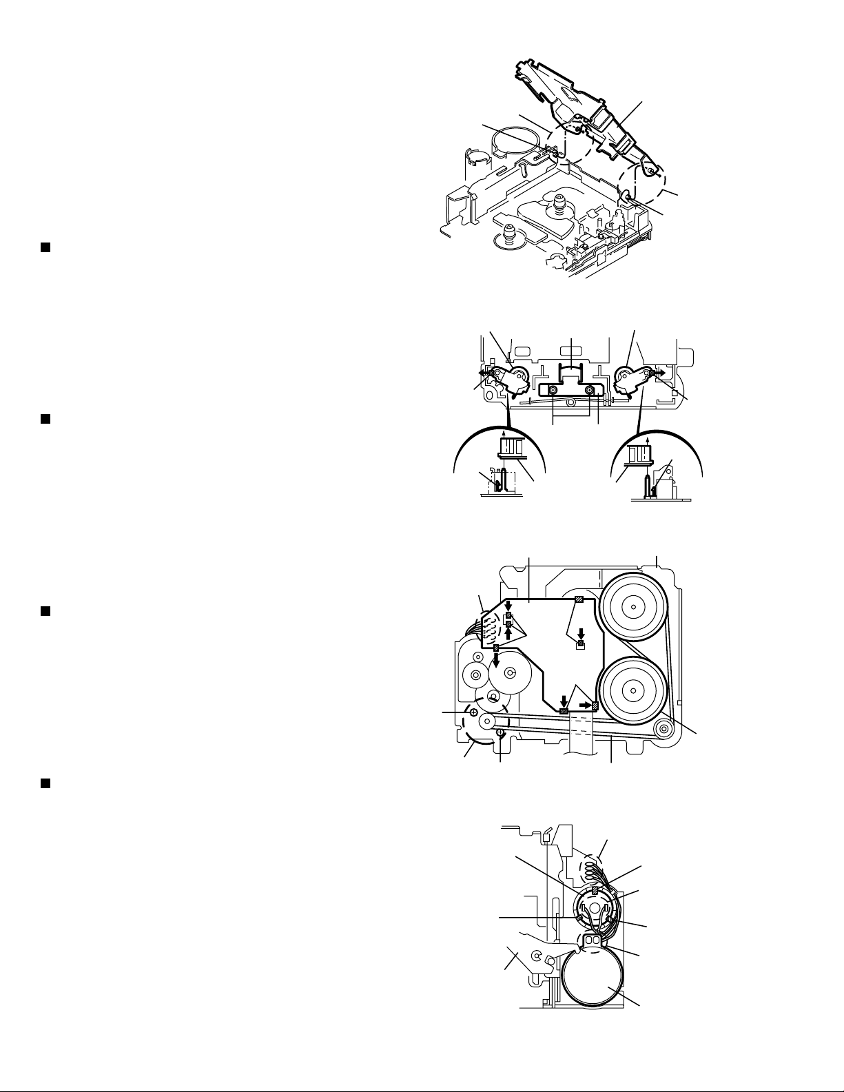
Removing the head relay P.W.B.
(See Fig.4)
1.
Unsolder the soldering b on the head relay P.W.B.
2.
Remove the screw C attaching the head relay P.W.B.
3.
Remove the head relay P.W.B. in the direction of the
arrow while releasing the two joints c.
Removing the load arm (See Fig.5)
1.
Remove the E washer attaching the load arm using
a pincette or something like that and remove the
spring d.
2.
Move the part of the load arm marked upwards to
release it from the axis of rotation. Then rotate the
load arm in the direction of the arrow to remove it
from the cach.
Fig.4
Cach
Load arm
Fig.5
Head relay P.W.B.
Soldering b
C
E washer
Joint c
Spring d
Removing the sub chassis (See Fig.6)
*
Prior to performing the following procedure, remove
the head relay P.W.B.
1.
Remove the screw D attaching the sub chassis.
2.
Push the tab e in the direction of the arrow to detach
the one side of the sub chassis. Then release the
sub chassis from the tab f.
Removing the cassette holder and the
holder arm in the eject mode
(See Fig.7 and 8)
*
Prior to performing the following procedure, remove
the head relay P.W.B., the load arm and the sub
chassis.
1.
Remove the screw E attaching the reinforce bracket.
2.
Remove the reinforce bracket.
Tab f
Sub chassis
Head relay
P.W.B.
D
Cassette mecha chassis
Cassette holder
Fig.6
Head relay P.W.B.
Tab e
Reinforce bracket
E
Reinforce
bracket
tab g
3.
Push the tab g fixing the cassette holder in the
direction of the arrow and open the cassette holder
and the holder arm upward until they stop at an
angle of 45 degrees. Move the two joints h to the
side and remove the cassette holder and the holder
arm from the shaft.
Joint h
Load arm
Holder arm
Fig.7
Joint h
1-7
Page 8
KS-FX834R
Removing the play head (See Fig.9)
*
Prior to performing the following procedure, remove
the head relay P.W.B.and the sub chassis.
1.
Remove the two screws F attaching the play head
(The spring under the play head comes off at the
same time).
Shaft
Joint h
Pinch roller ass’y
Fig.8
Play head
Cassette holder
and holder arm
Joint h
Shaft
Pinch roller ass’y
Removing the pinch roller ass’y
(See Fig.9)
*
Prior to performing the following procedure, remove
the head relay P.W.B. and the sub chassis.
1.
Push each tab i in the direction of the arrow and pull
out the pinch rollers on both sides.
Removing the reel disc P.W.B.
(See Fig.10)
1.
Unsolder the soldering j on the reel disc P.W.B.
2.
Push the seven tabs k on the bottom of the cassette
mechanism assembly in the direction of the arrow.
Removing the motor and the sub motor
(See Fig.10 and 11)
Tab i
Tab i
Soldering j
G
Motor
F
Pinch roller ass’y
Fig.9
Reel disc P.W.B.
Tabs k
Tabs k
G
Tab i
Spring
Tab i
Cassette mechanism ass’y
Flywheel
Belt
Fig.10
1.
Unsolder the two soldering l of the motor and the sub
motor.
2.
Release the sub motor from the three tabs m. Push
the sub motor upward and pull out it.
3.
Remove the belt on the bottom of the cassette
mechanism assembly and remove the two screws G
attaching the motor.
ATTENTION:
The motors can be detached before
removing the load arm.
1-8
Sub motor
Tab m
Load arm
Soldering j
Tab m
Soldering l
Tab m
Soldering l
Motor
Fig.11
Page 9

KS-FX834R
Removing the flywheel
(See Fig.10 and 12)
1.
Prior to performing the following procedure, remove
the head relay P.W.B, the load arm, the sub chassis,
the cassette holder, the holder arm and the reel disc
P. W. B .
2.
Remove the belt on the bottom of the cassette
mechanism ass’y.
3.
Remove the slit washer attaching the flywheel on the
upper side of the cassette mechanism ass’y and pull
out the flywheel downward. Then remove another
flywheel in the same way.
ATTENTION:
When reassembling, make sure to use
a new slit washer.
Removing the reel disc ass’y( )
(See Fig.12 to 14)
Soldering j
G
Motor
Plate
Reel disc P.W.B.
G
Slit washer
Tab k
Tab o
Cassette mechanism ass’y
Tab k
Belt
Fig.10
Reel driver
The part n
Tabs o
Flywheel
Reel disc
ass’y( )
Push aside
the gear
*
Prior to performing the following procedure, remove
the head relay P.W.B, the load arm, the sub chassis,
the cassette holder and the holder arm.
1.
Disengage the part n inside of the reel driver which
engages with the shaft, using a pincette or
something like that. Then remove the reel driver from
the shaft.
2.
Remove the reel driver spring and the reel table.
The part n
Slit washer
Shaft
Fig.13
The part n
Reel driver
Fig.12
Reel driver
Reel driver spring
Reel disc ass’y( )
Reel table
Fig.14
1-9
Page 10

KS-FX834R
Adjustment method
Test instruments required for adjustment
1. Digital oscilloscope(100MHz)
2. Frequency Counter meter
3. Electric voltmeter
4. Wow & flutter meter
5. Test Tapes
MC-109C
VT724
VT739 ............For playback frequency measurement
VT712 ....For wow flutter & tape speed measurement
VT703 ..................... For head azimuth measurement
6. Torque gauge .................... Cassette type for CTG-N
...................
.......................
For TAPE CURL confirmation
(without Pad type)
For DOLBY level measurement
(mechanism adjustment)
Measuring conditions(Amplifier section)
Power supply voltage .............. DC14.4V (10.5 - 16V)
Load impedance ........... 4 (2 Speakers connection)
Line out............................................................ 20k
Standard volume position
Balance and Bass,Treble volume .Fader
:Center(Indication"0")
Loudness,Dolby NR,Sound,Cruise:Off
following conditions. Playback the test tape VT721.
AM mode 999kHz/62dB,INT/400Hz,30%
modulation signal on receiving.
FM mono mode 97.5MHz/66dB,INT/400Hz,22.5kHz
deviation pilot off mono
FM stereo mode 1kHz,67.5kHz dev. pilot7.5kHz dev.
Output level 0dB(1 V,50 /open terminal)
1-10
Page 11

Arrangement of adjusting & test points
Cassette mechanism
(Surface)
Motor assembly
KS-FX834R
Tape speed adjust
Head section view
Azimuth screw A
(Forward)
Playback head
Azimuth screw B
(Reverse)
Azimuth screw B
(Reverse)
Azimuth screw A
(Forward)
Playback Head
1-11
Page 12

KS-FX834R
Main board
Information for using a car audio service jig
1. We're advancing efforts to make our extension cords common for all car audio products.
Please use this type of extension cord as follows.
2. As a U-shape type top cover is employed, this type of extension cord is needed to check operation of the
mechanism assembly after disassembly.
3. Extension cord : EXTKSRT002-18P ( 18 pin extension cord ) For connection between mechanism assembly
and main board assembly.
Check for mechanism driving section such as motor ,etc..
Disassembly method
1. Remove the bottom cover.
2. Remove the front panel assembly.
3. Remove the top cover .
4. Install the front panel.
5. Confirm that current is being carried by connecting
an extension cord jig.
Note
Available to connect to the CP701 connector when installing the front panel.
Cassette mechanism
to Cassette mechanism
Extension cord
EXTKSRT002-18P
Main board
Front panel assembly
to Main board
1-12
EXTKSRT002-18P
Page 13

Mechanism adjustment section
Item Adjusting & Confirmation Methods Adjust Std. Value
1. Tape running
adjustment
2. Azimuth
adjustment
confirmation
a) At Forward playmode, using mirror tape, make adjustment
with Azimuth screw A and Azimuth screw B, without curl of 4
parts of head tape guide.
b) At Reverse play mode, using mirror tape, make adjustment
with Azimuth screw A and Azimuth screw B, without tape
curl of 4 parts of head guide.
c) At Forward / Reverse play mode, make confirmation of no
tape curl of 4 parts of head tape guide.
a) At forward play mode, make adjustment of peak of Lch / Rch
output with Azimuth screw A.
* For Oscilloscope litharge corrugation, set 45 as standard.
b) At Reverse play mode, make adjustment of peak of Lch / Rch
output with Azimuth screw B.
* For Oscilloscope litharge corrugation, set 45 as standard.
c) With AC volt meter confirm the difference of output for 4ch
between Lch / Rch at forward play mode and Lch / Rch
Reverse play mode being within 3.0dB.
d) After operation, make confirmation of Lch / Rch azimuth
output being within 1.0dB from adjustment value.
KS-FX834R
Azimuth
screw A
Azimuth
screw B
2.Tape Speed and
Wow & Flutter
HEAD
Tape guide
OK
HEAD TAPE
1.Check to see if the reading of the frequency counter & W ow
flutter meter is within 2940-3090 Hz( FWD/REV ), and less
than 0.35% ( JIS RMS ).
2.In case of out of specification, adjust the motor with a builtin volume resistor .
Tape curl NG
0
Phase
Built-in
volume resistor
45
Tape Speed
2940-3090Hz
Wow&Flutter
Less than
0.35%
(JIS RMS)
3.Playback
Frequency
response
1.Play the test tape ( VT724 : 1kHz ) back and set the volume
position at 2V .
2.Play the test tape ( VT739 )back and confirm 0 3dB at1kHz/
10kHz and -4+2dB at 1kHz/63Hz.
3.When 10kHz is out of specification, it will be necessary to
read adjust the azimuth.
Speaker out
1kHz/10kHz
: 0dB 3dB,
63Hz/1kHz
: -4dB+2dB,
1-13
Page 14

KS-FX834R
Description of major ICs
CXA2560Q (IC401) : Dolby B type noise reduction system with play back equalizer amp.
1.Pin layout & block diagram
PBTC2
PBFB2
31
PBRIN2
32
PBGND
33
PBFIN2
34
VCT
35
PBREF
36
PBFIN1
37
PBGND
38
PBRIN1
39
PBFB1
40
2. Pin function
PBOUT2
30 29 28
7k/12k
300k
+
F2
30k
45k
30k
F1
+
-
300k
7k/12k
12345
PBTC1
PBOUT1
OUTREF2
27
x1
x1
70 /120 70 /120
OUTREF1
TAPEIN2
26
100k
T2
T1
100k
TAPEIN1
GND
Vcc
25
FWD/RVS
LPF
DIREF
+
BIAS
MUTE
TAPE EQ
Vcc
+
-
6
NC
LINEOUT2
24
OFF/B
-
F3
+
7
LINEOUT1
TCH2
NC
23 22 21
NR
MS MODE
NR MODE
DET
OFF/B
-
NR
8910
NC
TCH1
MS ON/
OFF
MSSW
MSLPF
20
19
18
17
16
15
14
13
12
11
MSMODE
DRSW
TAPESW
MUTESW
NRSW
NC
MSOUT
MSTC
G1FB
G2FB
Pin No. Symbol
1
2
3
4
5
6
7
8
9
10
11
12
13
14
15
16
17
18
19
20
21
22
23
24
PBTC1
PBOUT1
OUTREF1
TAPEIN1
Vcc
NC
LINEOUT1
TCH1
NC
MSLPF
G2FB
G1FB
MSTC
MSOUT
NC
NRSW
MUTESW
TAPESW
DRSW
MSMODE
MSSW
NC
TCH2
LINEOUT2
I/O Function
Playback equalizer amplifier
capacitance
Playback equalizer amplifier
O
output
Output reference
O
TAPE input
I
Power supply
-
Line output
O
Time constant for the HLS
-
Cut-off frequency adjustment
of the music sensor LPF
Music signal interval detection
Music signal interval detection
Time constant for detecting
music signal interval
Music sensor out
O
No use
Dolby NR control
I
Mute function control
I
Playback equalizer amplifier
I
control
Head select control
I
Music sensor mode control
I
Music sensor control
I
Time constant for the HLS
Line output
O
Pin No. Symbol
25
26
27
28
29
30
31
32
33
34
35
36
37
38
39
40
DIREF
GND
TAPEIN2
OUTREF2
PBOUT2
PBTC2
PBFB2
PBRIN2
PBGND
PBFIN2
VCT
PBREF
PBFIN1
PBGND
PBRIN1
PBFB1
I/O Function
-
Resistance for setting the
reference
-
Ground
I
TAPE input
O
Output reference
O
Playback equalizer amplifier
output
-
Playback equalizer amplifier
capacitance
I
Playback equalizer amplifier
feedback
I
Playback equalizer amplifier
input
-
Playback equalizer amplifier
ground
I
Playback equalizer amplifier
input
O
Center
O
Playback equalizer amplifier
reference
I
Playback equalizer amplifier
input
-
Playback equalizer amplifier
ground
I
Playback equalizer amplifier
input
I
Playback equalizer amplifier
feedback
1-14
Page 15

BA4905-V3 (IC901) : Regulator
1.Terminal layout
12 34 5678 9101112
2.Block diagram
KS-FX834R
REGULATOR
EXT
RESET
1 2 3 4 5 6 7 8 9 10 11 12
RESET COMP VDD 5.7V CD 8V VCC AJ
EXT ACC AUDIO 9V CTRL ILM 10V GND
3.Pin function
Pin no. Symbol Function
1
2
RESET
EXT output
If VDD voltage becomes 4V or less.RESET output becomes low level.
This output voltage is approximately 0.5V lower than VCC. and max
output current is 300mA.
3
COMP output
A voltage supply for ACC block. This output voltage is approximately
0.7V lower than VDD'S. The max output current is 100mA.
4
5
ACC
VDD output
Control of the COMP output by inputting voltage.
This output voltage is 5.7V, and max output current is 100mA.
This voltage supply is for microcomputer. Whenever back up voltage
supply is connected, the output keeps on running.
6
AUDIO output
This output voltage is 9.0v, and max output current is 500mA.
This voltage supply for AUDIO.
7
CD output
This output voltage is 8.0V, and max output current is 1A.
This voltage supply for CD.
8
9
10
CTRL
VCC
ILM output
Output selector of CD. AUDIO, ILM and EXT.
To be connected with the BACK UP of car.
This output voltage is 10V, and max output current is 500mA.
Output voltage is adjustable.
11
AJ
Putting a resistance between ILM and AJ or between AJ and GND
makes ILM output voltage adjustable.
12
GND
Ground.
Overvoltage
protection circuit
37K
5K
1-15
Page 16

KS-FX834R
UPD178018AGC-551 (IC701) : Main system control CPU
1. Pin layout
80 ~ 61
1
60
2. Pin function
Pin No.
1
2
3
4
5
6
7
8
9
10
11
12
13
14
15
16
17
18
19
20
21
22
23
24
25
26
27
28
29
30
31
32
33
34
35
36
37
38
39
40
~
20
21 ~ 40
~
41
Port Name I/O Descriptions
KEY 0
KEY 1
KEY 2
LEVEL
SM
SQ
LCDCE
LCDDA
LCDSCK
BUSI/O
OPEN
BUSSI
BUSSO
BUSSCK
NC
NC
NC
NC
INLOCK
NC
GNDPORT
VDDPORT
NC
AFCK
MONO
FM/AM
SEEK/STP
NC
IFC
VDDPLL
FMOSC
NC
GNDPLL
AMEO
FMEO
IC
SD/ST
STAGE0
NC
MOTOR
O
O
O
O
I/O
-
-
-
-
-
-
-
O
O
O
O
O
-
-
O
O
-
O
I
I
I
I
I
I
Key input 0
Key input 1
Key input 2
Level meter input
S.meter level input
S.Quality level input
CE output to LCD driver
Data output to LCD driver
Clock output to LCD driver
I
I
I
I/O selector output for J-BUS, H : OUT, L: INPUT
Door open detect input
J-BUS Data input
J-BUS Data output
J-BUS Clock in/output
Non connect
Non connect
Non connect
Non connect
Non connect
Non connect
Port GND
Port Vdd
Non connect
AF check output, L: AF check
Monaural on /off selecting output, H:mono on
FM/AM switching output L : FM H : AM
Auto seek /stop selecting output, H: Seek, L:Stop
I
I
Pulse signal input port for Cruise control
FM/AM midle frequency counter input
PLL Vdd
I
FM/AM limited generator frequency input
None connect
PLL GND
AM error out output
FM error out output
GND
I
I
Station detector, Stereo signal input, H:Find Station, L:Stereo
Pull up
Non connect
Main motor output
1-16
Page 17

UPD178018AGC-551
KS-FX834R
Pin No.
41
42
43
44
45
46
47
48
49
50
51
52
53
54
55
56
57
58
59
60
61
62
63
64
65
66
67
68
69
70
71
72
73
74
75
76
77
78
79
80
Port Name I/O Descriptions
FF/REW
F/R
DOLBY
MSIN
I2CCLK
I2CDAO
I2CDAI
REEL
SUBMO1
SUBMO2
MODE
TAPEIN
STANDBY
NC
NC
NC
NC
NC
BEEP
MUTE
PCNT
TELMUTE
DIMIN
DIMOUT
ENC1
ENC2
ACCDET
POWER
RDSSCK
RDSDA
REMOCON
DETACH
J-BUSINT
REGCPU
GND
X2
X1
REGOSC
VDD
RESET
I
O
O
I
O
O
I
O
I
O
O
O
I
-
-
-
-
O
O
O
I
I
O
I
I
I
O
I
I
I
I
I
-
-
-
I
-
-
-
Output for input signal level switching for MS L : FF,REW H : PLAY
FWD,REV running direction switch signal input
Dolby on "H" output
MS input
I2C information clock output
I2C information data output
I2C information clock input
Switch for detecting tape end position
Sub motor clock direction input
Sub motor clock opposite detection drive output
Mechanism mode position detection input
Cassette in detection input H : cassette in L : cassette out
Standby position detection input H : eject side L : operation side
Non connect
Non connect
Non connect
Non connect
Non connect
Touch tone output
Mute output , L : mute on
Power ON /OFF switching output , H : power on
Telephone mute signal detection input
Dimmer signal detection input L : dimmer
Dimmer control output , Dimmer off L output
Rotary volume signal 1 input Power save : L
Rotary volume signal 2 input
Power save 1 Working together ACC Power save : L
Power save 2, Working together Back up by H input, stop mode
Clock input for RDS
RDS data input
Remocom input
Detach signal input H : Power save
Cut-in input for J-BUS signal
Regulator for CPU power supply, Connect the GND with0.1 F.
Ground
Connecting the crystal oscillator for system clock
Connecting the crystal oscillator for system clock
Regulator for oscillator circuit.Connect the GND with 0.1 F.
Vdd
Pull up
1-17
Page 18

KS-FX834R
HA13158A (IC301) : Power amp
1. Pin layout
1 ~ 23
2. Block diagram
INVCC
IN1
2
STBY
1
14 18 6
PVCC1PVCC2
INPUTBUFFER1
AMP1
+
3
4
-
5
IN2
IN3
IN4
11
13
23
10
MUTE
INPUTBUFFER2
INPUTBUFFER3
INPUTBUFFER4
PROTECTOR (ASO
SURGE, TSD)
12 22
AMP2
AMP3
AMP4
TA B
7
+
8
-
9
15
+
16
-
17
19
+
20
-
21
1-18
Page 19

HD74HC126FP-X (IC801) : Buffer
KS-FX834R
1. Pin layout
1
2
3
4
5
6
7
3. Block diagram
Input
14
13
12
11
10
9
8
Vcc Vcc
1A
2A
3A
4A
1C
2C
3C
See Function Table
4C
2. Function
Output
1Y
2Y
Output
2Y
Output
3Y
Output
4Y
Inputs Outputs
C
A
L
X
H
L
H
H
1k
CL
Sample as Load Circuit 1
Sample as Load Circuit 1
Sample as Load Circuit 1
Y
Z
H
L
1k
S1
1-19
Page 20

KS-FX834R
RPM6938-SV4 (IC602) : Remote control receiver
AMP
I/V
conversion
PD
magnetic shield
LB1641 (IC402) : DC Motor Driver
1. Pin Layout
1 2 3 4 5 6 7 8 9
GND OUT1 P1
VZ IN1 IN2
VCC1
VCC2 P2
BPF
for
trimming
circuit
OUT2
AGC
2. Pin Functions
10
Vcc
Comp
Detector
Input Output
IN1 IN2 OUT1 OUT2
0 0 0 0
1 0 1 0
0 1 0 1
1 1 0 0
22k
ohm
Vcc
Rout
GND
Mode
Brake
CLOCKWISE
COUNTER-CLOCKWISE
Brake
1-20
Page 21

LC75873NW (IC601) : LCD Driver
1.Block Diagram
COM3
COM2
COM1
S68
S67
S5
S4/P4
S3/P3
S2/P2
S1/P1
KS-FX834R
VDD1
VDD2
INH
OSC
VDD
VSS
COMMOM
DRIVER
CLOCK
GENERATOR
SEGMENT DRIVER
SHIFT REGISTER
ADDRESS
DETECTOR
2.Pin Functions
Pin No. Symbol Description
1~66
67~69
70
71
S3~S68
COM1~3
VDD
VDD1
I/O
Segment Output.
O
Common Driver Output.
O
Power Supply Connection.
Used for applying the LCD drive 2/3 bias voltage externally.
I
Must be connected to VDD2 when a 1/2 bias drive scheme in used.
72
VDD2
Used for applying the LCD drive 1/3 bias voltage externally.
I
Must be connected to VDD1 when a 1/2 bias drive scheme in used.
73
74
VSS
OSC
Power supply connection.
Oscillator connection. An oscillator circuit is formed by connecting an
I/O
external resistor and capacitor to this pin.
75
76
77
78
79
80
INH
CE
CLOCK
DI
DIMMER
NC
Display off control input.
I
Chip enable input.
I
Synchronization clock input.
I
Serial data input.
I
DIMMER Control signal output.
O
Non connect.
-
1-21
Page 22

KS-FX834R
SAA6579T-X (IC71) : RDS demodulator
1. Pin layout 2. Pin function
1
2
3
4
5
6
7
8
16
15
14
13
12
11
10
9
Pin
Symbol Function
No.
1
2
3
4
5
6
7
8
9
10
11
12
13
14
15
16
QUAL
RDDA
Vref
MUX
VDDA
VSSA
CIN
SCOUT
MODE
TEST
VSSD
VDDD
OSCI
OSCO
T57
RDCL
Quality indication output
RDS data output
Reference voltage output (0.5VDDA)
Multiplex signal input
+5V supply voltage for analog part
Ground for analog part (0V)
Sub carrier input to comparator
Sub carrier output of reconstruction filter
Oscillator mode / test control input
Test enable input
Ground for digital part (0V)
+5V supply voltage for digital part
Oscillator input
Oscillator output
57kHz clock signal output
RDS clock output
3. Block diagram
CIN
Vref
4
8
7
5
3
MUX
SCOUT
VDDA
ANTI-
ALIASING
FILTER
CLOCKED
COMPARATOR
Vp1
REFERENCE
VOLTAGE
6
57kHz
BAND PASS
(8th ORDER)
COSTAS LOOP
VARIABLE AND
FIXED DIVIDER
CLOCK
REGENERATION
AND SYNC
RECONSTRUCTION
FILTER
TEST LOGIC AND OUTPUT
OSCI OSCO VDDD
13 14 12
OSCILLATOR
AND
DIVIDER
BIPHASE
SYMBOL
DECODER
SELECTOR SWITCH
91011
QUALITY BIT
GENERATOR
DIFFERENTIAL
DECODER
VSDDTESTMODEVSSA
16
15
1
2
QUAL
RDDA
RDCL
T57
1-22
Page 23

TEA6320T-X (IC161) : E.volume
1.Pin Layout
2.Block Diagram
10 8 9 7 6
KS-FX834R
5
12
SDA
1
GND
2
OUTLR
OUTLF
MUTE
TL
B2L
B1L
IVL
ILL
QSL
IDL
ICL
IMD
IBL
IAL
3
4
5
6
7
8
9
10
11
12
13
14
15
16
3.Pin Functions
Pin
Symbol
No.
SDA
1
SCL
32
VCC
31
OUTRR
30
OUTRF
29
TR
28
B2R
27
B1R
26
IVR
25
ILR
24
QSR
23
IDR
22
Vref
21
ICR
CD-CH
TAPE
TUNER
20
19
18
17
CAP
IBR
IAR
I/O
Serial data input/output.
I/O
MUTE
21
31
2
19
16
15
13
11
14
22
20
18
17
Functions Functions
POWER
SUPPLY
SOURCE
SELECTOR
23 25 24 26 27 28
VOLUME 1
+20 to -31 dB
LOUDNESS
LEFT
VOLUME 1
+20 to -31 dB
LOUDNESS
RIGHT
Pin
No.
17
Symbol
IAR
BASS
LEFT
+15 dB
LOGIC
BASS
RIGHT
+15 dB
I/O
I
Input A right source.
TREBLE
LEFT
+12 dB
TREBLE
RIGHT
+12 dB
FUNCTION
ZERO CROSS
DETECTOR
VOLUME 2
0 to 55 dB
BALANCE
FENDER REAR
VOLUME 2
0 to 55 dB
BALANCE
FENDER FRONT
HC BUS
REC
VOLUME 2
0 to -55dB
BALANCE
FENDER FRONT
VOLUME 2
0 to -55dB
BALANCE
FENDER REAR
3
4
32
1
29
30
2
3
4
5
6
7
8
9
10
11
12
13
14
15
16
GND
OUTLR
OUTLF
TL
B2L
B1L
IVL
ILL
QSL
IDL
MUTE
ICL
IMO
IBL
IAL
Ground.
-
output left rear.
O
output left front.
O
Treble control capacitor left channel or
I
input from an external equalizer.
Bass control capacitor left channel or
-
output to an external equalizer.
Bass control capacitor left channel.
-
Input volume 1. left control part.
I
Input loudness. left control part.
I
Output source selector. left channel.
O
Not used
-
Not used
-
Input C left source.
I
Not used
-
Input B left source.
I
Input A left source.
I
18
19
20
21
22
23
24
25
26
27
28
29
30
31
32
IBR
CAP
ICR
Vref
IDR
QSR
ILR
IVR
B1R
B2R
TR
OUTRF
OUTRR
Vcc
SCL
I
Input B right source.
-
Electronic filtering for supply.
I
Input C right source.
-
Reference voltage (0.5Vcc)
-
Not used
O
Output source selector right channel.
I
Input loudness right channel.
I
Input volume 1. right control part.
-
Bass control capacitor right channel
Bass control capacitor right channel or
O
output to an external equalizer.
Treble control capacitor right channel or
I
input from an external equalizer.
O
Output right front.
O
Output right rear.
-
Supply voltage.
I
Serial clock input.
1-23
Page 24

KS-FX834R
VICTOR COMPANY OF JAPAN, LIMITED
MOBILE ELECTRONICS DIVISION
PERSONAL & MOBILE NETWORK B.U. 10-1,1Chome,Ohwatari-machi,Maebashi-city,Japan
(No.49571)
Printed in Japan
200009(V)
 Loading...