

Page 1
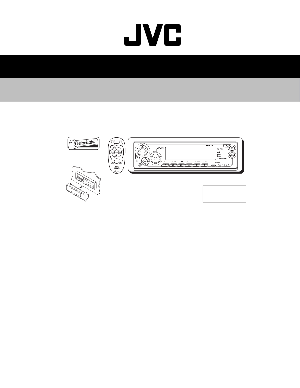
KS-FX8
SERVICE MANUAL
CASSETTE RECEIVER
4982620034
KS-FX8
Area Suffix
UN ----------- Asean
TABLE OF CONTENTS
1 Important Safety Precautions . . . . . . . . . . . . . . . . . . . . . . . . . . . . . . . . . . . . . . . . . . . . . . . . . . . . . . . . . . . 1-2
2 Disassembly method . . . . . . . . . . . . . . . . . . . . . . . . . . . . . . . . . . . . . . . . . . . . . . . . . . . . . . . . . . . . . . . . . . 1-3
3 Adjustment method. . . . . . . . . . . . . . . . . . . . . . . . . . . . . . . . . . . . . . . . . . . . . . . . . . . . . . . . . . . . . . . . . . . 1-11
4 Description of major ICs. . . . . . . . . . . . . . . . . . . . . . . . . . . . . . . . . . . . . . . . . . . . . . . . . . . . . . . . . . . . . . . 1-15
COPYRIGHT © 2003 VICTOR COMPANY OF JAPAN, LTD.
No.49826
2003/4
Page 2

KS-FX8
1.1 Safety Precautions
SECTION 1
Important Safety Precautions
!
Burrs formed during molding may be left over on some parts of the chassis. Therefore,
pay attention to such burrs in the case of preforming repair of this system.
1-2 (No.49826)
Page 3
SECTION 2
Disassembly method
2.1 Main body
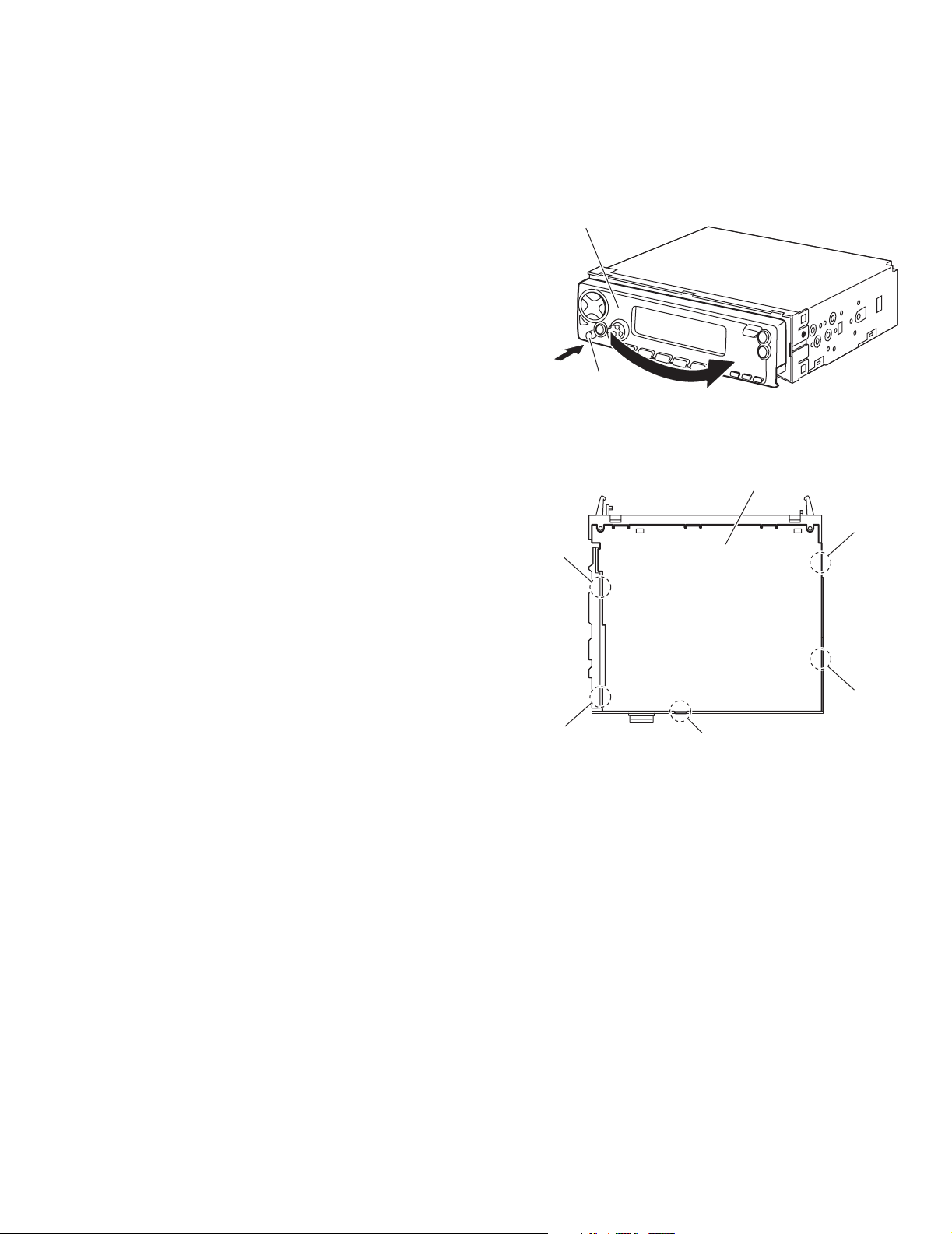
2.1.1 Removing the front panel assembly
(See Fig.1)
(1) Push the detach button in the lower left part of the front
panel assembly and remove the front panel assembly in
the direction of the arrow.
2.1.2 Removing the bottom cover
(See Fig.2)
• Prior to performing the following procedures, remove the front
panel assembly.
(1) Turn the main body upside down.
(2) Insert a screwdriver under the joints to release the two
joints a on the left side, two joints b on the right side and
joint c on the back side of the main body, then remove the
bottom cover from the main body.
CAUTION:
When releasing the joints using a screwdriver, do not damage
the main board.
KS-FX8
Front panel assembly
Detach button
Fig.1
Bottom cover
Joint b
Joint a
Joint a
Joint b
Joint c
Fig.2
(No.49826)1-3
Page 4

KS-FX8
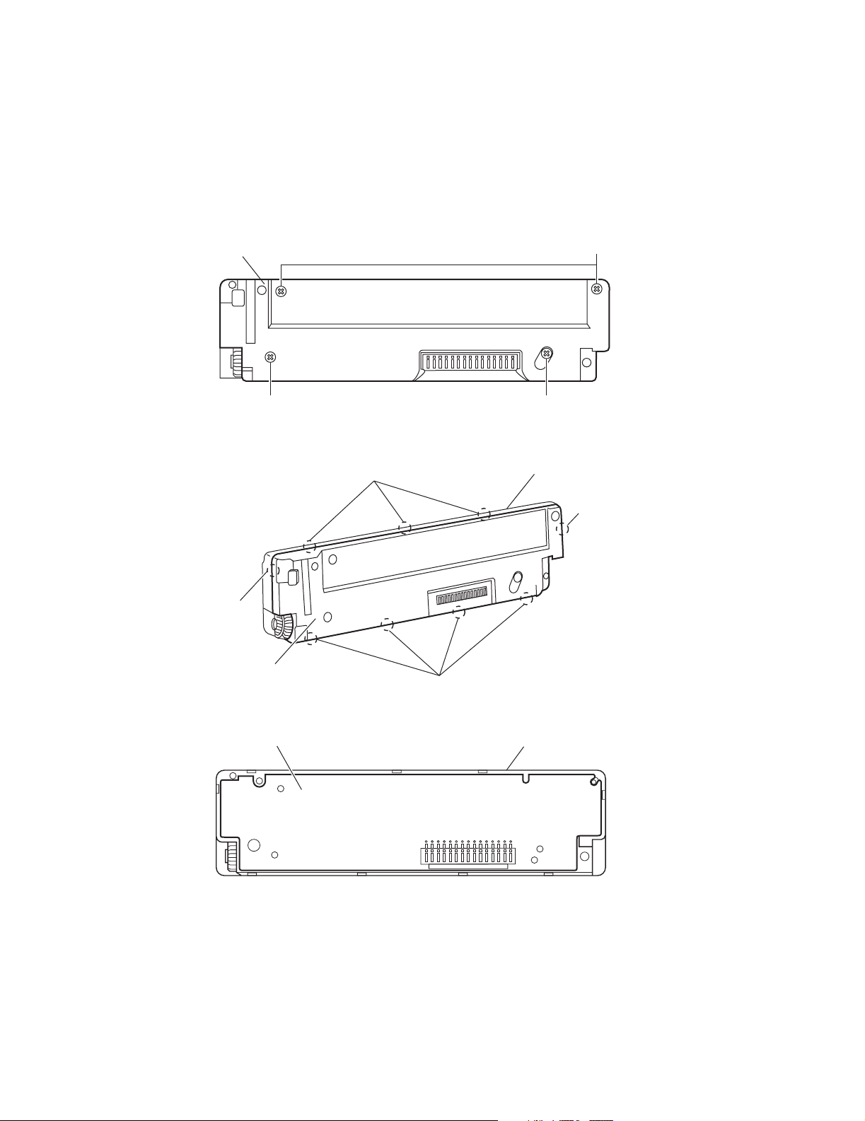
2.1.3 emoving the front chassis assembly
(See Figs.3 and 4)
• Prior to performing the following procedures, remove the front
panel assembly and bottom cover.
(1) Remove the two screws A on the both sides of the main
body. (See Fig.3.)
(2) Remove the two screws B on the front side of the main
body. (See Fig.4.)
(3) Release the two joints d and two joints e on the both sides
of the main body, then remove the front chassis assembly
toward the front. (See Fig.3.)
Joint d
A
Joint e
A
2.1.4 Removing the heat sink
(See Fig.5)
• Prior to performing the following procedure, remove the front
panel assembly.
(1) Remove the two screws C and two screws D attaching the
heat sink on the left side of the main body, and remove the
heat sink.
Joint d
Front chassis assembly
B
Joint e
Fig.3
Front chassis assembly
Fig.4
C
2.1.5 Removing the rear panel
(See Fig.6)
• Prior to performing the following procedure, remove the front
panel assembly and bottom cover.
(1) Remove the two screws E, screws F and five screws G at-
taching the rear panel on the back side of the main body.
1-4 (No.49826)
D
Heat sink
Fig.5
GG
EE
Rear bracket
F
Fig.6
Page 5

2.1.6 Removing the main board
(See Fig.7)
• Prior to performing the following procedures, remove the front
panel assembly, bottom cover, front chassis assembly, heat
sink and rear panel.
(1) Remove the two screws H attaching the main board on the
top chassis.
(2) Disconnect the connector CP701 on the main board from
the cassette mechanism assembly.
2.1.7 Removing the cassette mechanism assembly
(See Fig.8)
• Prior to performing the following procedures, remove the front
panel assembly, bottom cover, front chassis assembly, heat
sink, rear panel and main board.
(1) Disconnect the card wire from the connector CN403 on the
mecha board.
(2) Remove the four screws J attaching the cassette mecha-
nism assembly from the top chassis, take out the cassette
mechanism assembly.
(3) From the bottom side of the cassette mechanism assem-
bly, disconnect the wire from the connector on the head
board.
KS-FX8
Main board
H
CP701
Fig.7
Cassette mechanism assembly
J
H
J
Connector
Head board
2.1.8 Removing the mecha board
(See Fig.9)
• Prior to performing the following procedures, remove the front
panel assembly, bottom cover, front chassis, heat sink, rear
panel, main board and cassette mechanism assembly.
(1) Remove the screw K attaching the mecha board.
(2) Bend the hook f in the direction of the arrow 1 and move the
mecha board in the direction of the arrow 2.
(3) Remove the mecha board from the mecha bracket (L) of
the top chassis.
Mecha board
Top chassis
K
J J
CN403
Fig.8
Mecha board
Fig.9
Top chassis
Hook e
1
2
Mecha bracket (L)
(No.49826)1-5
Page 6
KS-FX8
f
2.1.9 Removing the front board
(See Figs.10 to 12)
• Prior to performing the following procedures, remove the front
panel assembly.
(1) Remove the four screws L attaching the rear cover on the
back side of the front panel assembly. (See Fig.10.)
(2) Release the nine joints g, the front panel assembly and the
rear cover become separate. (See Fig.11.)
(3) Remove the front board from the front panel assembly.
(See Fig.12.)
Rear cover
Joint f
L
Joints f
L
L
Fig.10
Front panel assembly
Joint
Rear cover
Front board
Joints f
Fig.11
Front panel assembly
Fig.12
1-6 (No.49826)
Page 7
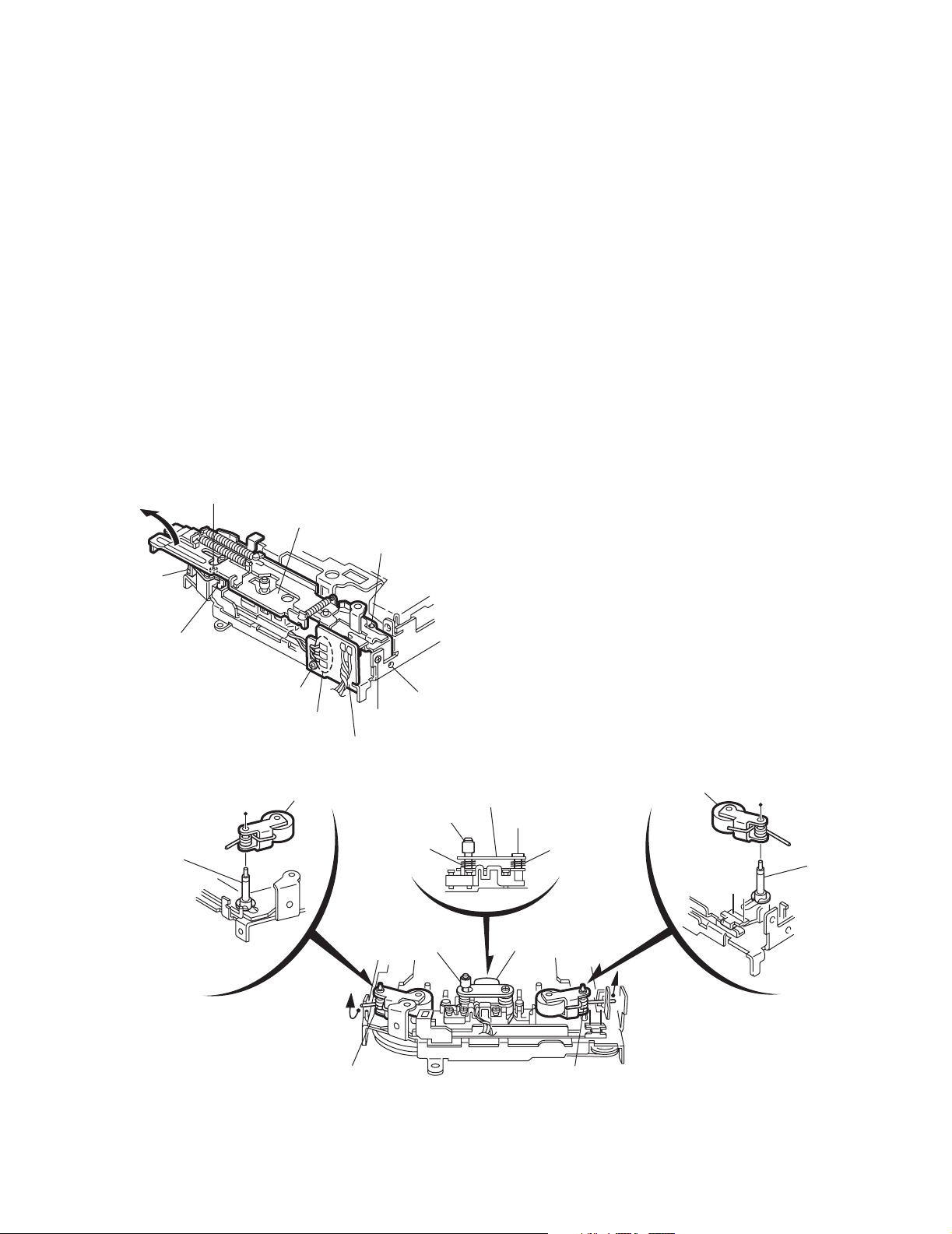
2.2 Cassette mechanism assembly
• Prior to performing the following procedures, remove the head
amplifier board, the relay board and the mechanism bracket.
2.2.1 Removing the direction switch board
(See Fig.1)
(1) Unsolder the three wires a on the direction switch board.
(2) Remove the one screw A attaching the direction switch
board.
2.2.2 Removing the FF / REW lever assembly
(See Fig.1)
(1) Remove the screw B attaching the FF / REW lever assem-
bly on the back of the cassette mechanism assembly.
(2) Remove the screw C on the upper side of the FF / REW le-
ver assembly.
(3) Lift and pull forward the FF / REW lever assembly to disen-
gage the joints b, c, d and e.
2.2.3 Reattaching the FF / REW lever assembly
(See Fig.1)
(1) Reattach the FF / REW lever assembly to the joint c on the
back of the chassis.
(2) Reattach the pinch-roller shaft e, the change lever d and
the return link e to the chassis.
C
FF / REW lever assembly
Joint c
KS-FX8
2.2.4 Removing the playback head
(See Fig.2)
• Prior to performing the following procedure, remove the direc-
tion switch board and the FF / REW lever assembly.
(1) Remove the screw D attaching the playback head.
(2) Remove the C washer and pull out the FF roller.
(3) Remove the S support plate, the A arm spring (a) and (b),
the playback head.
ATTENTION:
The A arm spring (a) differs from the A arm spring (b).
2.2.5 Removing the pinch-roller (R) and (F) assembly
(See Fig.2)
• Prior to performing the following procedure, remove the direc-
tion switch board and the FF / REW lever assembly.
(1) Remove the P arm spring (f) in the pinch-roller (F) assem-
bly from the chassis.
(2) Remove the P arm spring (r) in the pinch-roller (R) assem-
bly from the chassis.
(3) Draw out the pinch roller (F) and (R) assembly from the
shaft.
ATTENTION:
The P arm spring (f) differs from the P arm spring (r).
ATTENTION:
The pinch roller (F) assembly differs from the pinch roller (R)
assembly.
Joint e
Joint d
A
Soldering a
Direction switch board
Fig.1
Pinch-roller (R) assembly
Shaft
Remove the P arm spring (r)
from the chassis.
Joint b
B
C washer
A arm spring (b)
FF roller
S support plate
D
Playback head
Pinch-roller (F) assembly
A arm spring (a)
Shaft
Remove the P arm spring (f)
from the chassis.
P arm spring (r)
P arm spring (f)
Fig.2
(No.49826)1-7
Page 8
KS-FX8
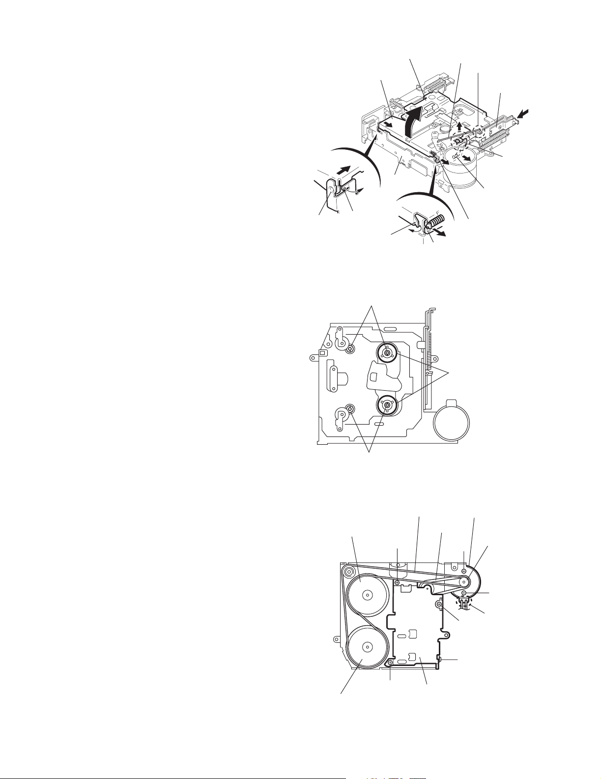
2.2.6 Removing the cassette hanger / cassette holder
(See Fig.3)
• Prior to performing the following procedure, remove the FF /
REW lever assembly.
(1) From the rear of the unit, bend the two tabs f outwards and
disengage the two joints g in the direction of the arrow.
(2) Push the eject lever and remove the cassette holder from
the playback head. Disengage the two joints h of the cassette hanger / cassette holder and the eject lever in the direction of the arrow.
(3) Lift the cassette hanger / cassette holder and disengage
the joint i of the return link and the eject lever.
2.2.7 Removing the reel disc assembly
(See Fig.4)
• Prior to performing the following procedure, remove the FF /
REW lever assembly and the cassette hanger / cassette holder.
(1) Remove the C washer and pull out reel disc assembly.
ATTENTION:
Replace with a new C washer when reattaching.
Joint g
Cassette holder
Cassette hanger
Chassis
Tab f
Tab f
C washer
Return link
Joint i
Eject lever
Joint h
Joint h
Joint g
Fig.3
2.2.8 Removing the motor assembly
(See Fig.5)
(1) Unsolder the two wires j on the motor assembly.
(2) Turn over the cassette mechanism assembly and remove
the main belt and the sub-belt from the motor pulley.
ATTENTION:
The main belt can now be removed.
(3) Remove the two screws G attaching the motor assembly.
C washer
Flywheel (BF)
Fig.4
Main-belt
E
Reel disc assembly
Motor assembly
Sub-belt
G
E
Motor pulley
G
Soldering j
1-8 (No.49826)
Flywheel (BR)
Reel base assembly
E
Fig.5
F
Page 9

KS-FX8
2.2.9 Removing the Flywheel (BF) and (BR) assembly
(See Fig.4 and 5)
• Prior to performing the following procedure, remove the cas-
sette hanger / cassette holder.
(1) From the upper side of the cassette mechanism assembly,
remove the C washer from each shaft of the flywheel (BF)
and (BR).
(2) Turn over the cassette mechanism assembly and remove
the main belt. Pull out the flywheel (BF) and (BR) downward respectively.
C washer
Reel disc assembly
C washer
Fig.4
2.2.10 Removing the reel base assembly
(See Fig.5 and 6)
(1) Raise the part k of the reel base assembly slightly and re-
move the selector link (B) on the front side of the cassette
mechanism assembly by turning it as shown in Fig.6.
(2) Remove the three screws E and the one screw F on the un-
derside of the cassette mechanism assembly.
ATTENTION:
The reel base assembly is not repairable. Handle with care.
Pinch-roller (R) assembly
k
Selector link (B).
Turn the selector link (B).
Fig.6
Inside of the reel base assembly
Flywheel (BF)
Flywheel (BR)
Main-belt
Sub-belt
E
Reel base assembly
E
Fig.5
Motor assembly
Motor pulley
G
G
Soldering j
E
F
Fig.7
(No.49826)1-9
Page 10

KS-FX8
2.2.11 Removing the mute switch board
(See Fig.8)
(1) Unsolder the two wires l on the mute switch board on the
back of the cassette mechanism assembly.
(2) Remove the screw H attaching the mute switch board.
2.2.12 Removing the power switch
(See Fig.9)
• Prior to performing the following procedure, remove the motor
assembly.
(1) Unsolder the two wires m on the power switch on the side
of the cassette mechanism assembly.
(2) Remove the screw I attaching the power switch.
Cassette mechanism assembly
Soldering l
H
Fig.8
Soldering m
I
Cassette mechanism assembly
Power switch
Fig.9
Rower switch
Motor assembly
Mute switch board
1-10 (No.49826)
Page 11

SECTION 3
Adjustment method
Test instruments required for adjustment Standard volume position
1. Digital oscilloscope (100MHz)
2. Frequency counter meter
3. Electric voltmeter
4. Wow & flutter meter
5. Test tapes
VT724.......................for DOLBY level measurement
VT739............For playback frequency measurement
VT712....For wow flutter & tape speed measurement
VT703.....................For head azimuth measurement
6. Torque gauge...................Cassette type for CTG-N
(Mechanism adjustment)
Measuring conditions (Amplifier section)
Balance and Bass, Treble volume, Fader
: Center (Indication "0")
Loudness, Dolby NR, Sound, Cruise : Off
Volume position is about 2V at speaker output with
following conditions, Playback the test tape VT721.
AM mode 999kHz/62dB, INT/400Hz, 30%
modulation signal on receiving.
FM mono mode 97.9MHz/66dB, INT/400Hz, 22.5kHz
deviation pilot off mono
FM stereo mode 1kHz, 67.5kHz dev. pilot 7.5kHz dev.
Output level 0dB (1 V,50 /open terminal)
KS-FX8
Power supply voltage.............. DC14.4V (11V to 16V allowance)
Load impedance............ 4 (4 to 8 allowance)
Line out level/Impedance..............1.0V/20k load (250 nWb/m)
Frequency band
Band
FM
AM
87.5 MHz to 108.0MHz
531 kHz to 1602 kHz
(No.49826)1-11
Page 12

KS-FX8
Information for using a car audio service jig
1. We're advancing efforts to make our extension cords common for all car audio products.
Please use this type of extension cord as follows.
2. As a U-shape type top cover is employed, this type of extension cord is needed to check operation of the
mechanism assembly after disassembly.
3. Extension cord : EXTKSRT002-18P ( 18 pin extension cord ) For connection between mechanism assembly
and main board.
4. Check for mechanism driving section such as motor ,etc.
D
i
sassembl
1. Remove the front panel assembly.
2. Remove the bottom cover.
3. Remove the front chassis assembly.
4. Remove the heat sink.
5. Remove the rear panel
6. Remove the main board.
7. Reattach the heat sink with the two screws D. (Refer to Disassembly method.)
8. Reattach the rear panel with the screw G. (Refer to Disassembly method.)
9. Reattach the front chassis assembly with the screw B. (Refer to Disassembly method.).
10. Reattach the front panel assembly.
11. Confirm that current is being carried by connecting an extension cord jig.
Note
Available to connect to the CJ701 connector when installing the front panel.
y met
hod
CAUTION :
Be sure to attach the heat sink and rear panel on the power amplifier IC and regulator IC
of a main board when supplying the power.
If voltage is applied without attaching those parts, the power amplifier IC and regulator IC
will be destroyed by heat.
To
Cassette mechanism
Extension cord
EXTKSRT002-18P
To
Main board
EXTKSRT002-18P
Cassette mechanism
1-12 (No.49826)
Front panel assembly
Main board
Page 13

Arrangement of adjusting & test points
A
Cassette mechanism
(Surface)
Motor assembly
Tape speed adjust
KS-FX8
Azimuth screw
(Forward)
Playback head
Head section view
Azimuth screw B
(Reverse)
Azimuth screw B
(Reverse)
Playback head
Azimuth screw A
(Forward)
(No.49826)1-13
Page 14

KS-FX8
Item
Head
1.
azimuth
adjustment
Conditions
Test tape:
SCC-1659
VT703 (10kHz)
Test tape:
VT724 (1kHz)
VT703 (10kHz)
VT721 (315Hz)
Adjustment and Confirmation methods
Head height adjustment
Adjust the azimuth directly. When you
adjust the height using a mirror tape,
remove the cassette housing from the
mechanism chassis. After installing the
cassette housing, perform the azimuth
adjustment.
Load the SCC-1659 mirror tape. Adjust with
1.
height adjustment screw A and azimuth
adjustment screw B so that line A of the
mirror tape runs in the center between Lch
and Rch in the reverse play mode.
After switching from REV to FWD then to
2.
REV, check that the head position set in
procedure 1 is not changed. (If the position
has shifted, adjust again and check.)
Adjust with azimuth adjustment screw B so
3.
that line B of the mirror tape runs in the
center between Lch and Rch in the forward
play mode.
Head azimuth adjustment
Load VT724 (1kHz) and play it back in
1.
the reverse play mode.
Set the Rch output level to max.
Load VT703 (10kHz) and play it back in
2.
the forward play mode. Adjust the Rch
and Lch output levels to max, with
azimuth adjustment screw B. In this case,
the phase difference should be within 45 .
Engage the reverse mode and adjust the
3.
output level to max, with azimuth
adjustment screw C.
(The phase difference should be 45 or
more.)
When switching between forward and
4.
reverse modes, the difference between
channels should be within 3dB. (Between
FWD L and R, REV L and R.)
S.Values Adjust
A line
Head shield
The head is at low position
during.
B line
Head shield
The head is at High position
during REV.
Output
level:
Maximum
PBHead
FWD Adj B
REV Adj C
(0 ) (45 )
HEIGHT Adj A
phase
Tape speed
2.
and wow
flutter
confirmation
Play back
3.
frequency
response
confirmation
1-14 (No.49826)
When VT721 (315Hz) is played back,
5.
the level difference between channels
should be within 1.5dB.
Test tape: VT712
(3kHz)
Test tape: VT724
(1kHz)
VT739
(63Hz / 1kHz / 10kHz)
The tuner section is of an adjustment-freedesign. In case the tuner is in trouble, replace the tuner pack.
Check to see if the reading of the F, counter /
1.
wow flutter meter is within 3015Hz to 3045Hz
(FWD/ REV), and less than 0.35% (JIS RMS).
In case of out of specification, adjust the
2.
motor with a built-in volume resistor.
Play test tape VT724, and set the volume
1.
position at 2V.
Play test tape VT739 and confirm.
2.
1kHz / 10kHz: -1 3dB,
1kHz / 63Hz: 0 3dB,
When 10kHz is out of specification, it will be
3.
necessary to read adjust the azimuth.
Tape speed:
3015Hz
to 3045Hz
Wow
flutter: less
than 0.35%
Speaker out
1kHz / 63Hz
: 0 3dB
1kHz / 10kHz
: -1 3dB
Built-in volume
resistor
Page 15

4.1 AN80T05 (IC901) : Regulator
• Pin layout & Block diagram
Reference Voltage
Thermal
Protection
SECTION 4
Description of major ICs
ASO & Peak
Current Protection
KS-FX8
Pre
Drive
Pre
Drive
AMP
Out
AMP
Out
123456789101112
ILL
MODE2 MODE1 STB VDD
10V
5.6V
AMP VCC ANT COM
• Pin function
Pin No. Symbol Function
1 ILL 10V power supply for illumination.
2 MODE2 When 5V is input, becomes AM. and the antenna output is turned on.
3 MODE1 When 5V is input,becomes AM. and the output of FM is switched.
4 STB When 5V is input outputs to ILL,COM, and AMP. It is 0V usually.
5 VDD 5.6V power supply.
6 AMP Power supply supply to remote amplifier
7 VCC Back up. connects with ACC with it.
8 ANT Power supply supply to auto antenna.
9 COM 8.7V power supply.
10 AM The power supply of 8.7V to AM.
11 FM The power supply of 8.7V to FM.
12 GND Ground
Pre
Drive
Pre
Drive
8.7VAM8.7VFM8.7V
Pre
Drive
GND
(No.49826)1-15
Page 16

KS-FX8
M
S
P
T
S
O
T
F
F
4.2 CXA2560Q (IC401) : Dolby B type noise reduction system with play back equalizer amp.
• Pin layout & block diagram
PBFB2
PBRIN2
PBGND
PBFIN2
VCT
PBREF
PBFIN1
PBGND
PBRIN1
PBFB1
PBTC2
30 29 28
7k/12k
31
32
33
34
35
45k
36
37
38
39
40
12345
C1
300k
F2
30k
30k
F1
300k
7k/12k
PBOUT2
+
+
-
T1
OUTREF2
TAPEIN2
27
100k
70 /120
T2
1
1
T1
100k
70 /120
F1
N1
GND
26
cc
DIREF
25
BIAS
MUTE
TAPE EQ
FWD/RVS
Vcc
LPF
6
NC
LINEOUT2
23 22 21
24
OFF/B
+
-
+
-
F3
OFF/B
-
+
8910
7
T1
TCH2
NR
MS MODE
NR MODE
DET
NR
H1
NC
MS ON/
OFF
NC
• Pin function
Pin No. Symbol I/O Function
1 PBTC1 - Playback equalizer amplifier
capacitance
2 PBOUT1 O Playback equalizer amplifier
output
3 OUTREF1 O Output reference
4 TAPEIN1 I TAPE input
5 Vcc - Power supply
6NC-
7 LINEOUT1 O Line output
8 TCH1 - Time constant for the HLS
9NC-
10 MSLPF - Cut-off frequency adjustment
of the music sensor LPF
11 G2FB - Music signal interval detection
12 G1FB - Music signal interval detection
13 MSTC - Time constant for detecting
music signal interval
14 MSOUT O Music sensor out
15 NC - No use
16 NRSW I Dolby NR control
17 MUTESW I Mute function control
18 TAPESW I Playback equalizer amplifier
control
19 DRSW I Head select control
20 MSMODE I Music sensor mode control
21 MSSW I Music sensor control
22 NC -
23 TCH2 - Time constant for the HLS
24 LINEOUT2 O Line output
1-16 (No.49826)
MSSW
20
19
18
17
16
15
14
13
12
11
PF
MS
DR
TA
MU
NR
NC
MS
MS
G1
G2
Pin No. Symbol I/O Function
25 DIREF - Resistance for setting the
reference
26 GND - Ground
27 TAPEIN2 I TAPE input
28 OUTREF2 O Output reference
29 PBOUT2 O Playback equalizer amplifier
output
30 PBTC2 - Playback equalizer amplifier
capacitance
31 PBFB2 I Playback equalizer amplifier
feedback
32 PBRIN2 I Playback equalizer amplifier
input
33 PBGND - Playback equalizer amplifier
ground
34 PBFIN2 I Playback equalizer amplifier
input
35 VCT O Center
36 PBREF O Playback equalizer amplifier
reference
37 PBFIN1 I Playback equalizer amplifier
input
38 PBGND - Playback equalizer amplifier
ground
39 PBRIN1 I Playback equalizer amplifier
input
40 PBFB1 I Playback equalizer amplifier
feedback
Page 17

4.3 HD74HC126P (IC801) : Buffer
c
Y
Y
Y
Y
•Pin layout •Pin function
Input Output
11C
21A
31Y
14
13
12
Vc
4C
4A
CA Y
LX Z
HL L
HH H
KS-FX8
• Block diagram
42C
52A
62Y
7GND
11
10
4Y
3C
9
3A
8
3Y
( TOP VIEW )
1A
1
1C
2A
2
2C
3A
3C
4A
4C
3
4
(No.49826)1-17
Page 18

KS-FX8
4.4 KIA7810PI (IC902) : Regulator
• Pin layout
• Block diagram
1 2 3
1 INPUT
R4 R18
Q12
R5
Z1
R6
R7
R1
Q1
Q13
R10 R3
Q8
Q10
Q5
Q7
R8
R2
Q6
Q2
R15
Q14
C1
R14
Q4
R9
Q9
R16
Q15
Q3
Q11
R13
R21
R17
Q16
R12
Q17
R11
3 OUTPUT
R20
R19
2 GND
1-18 (No.49826)
Page 19

4.5 LB1641 (IC402) : DC Motor driver
•Pin layout •Pin function
Input Output
IN1 IN2 OUT1 OUT2
0000 Brake
1 2 3 4 5 6 7 8 9
GND OUT1 P1
VZ IN1 IN2
VCC1
VCC2 P2
10
OUT2
1 0 1 0 CLOCKWISE
0 1 0 1 COUNTER-CLOCKWISE
1100 Brake
4.6 RPM6938-SV4 (IC602) : Remote control receiver
• Block diagram
Vcc
I/V
conversion
PD
magnetic shield
AMP
BPF
for
trimming circuit
AGC
Detector
Comp
22k
ohm
3
1
2
KS-FX8
Mode
VDD
OUT
GND
(No.49826)1-19
Page 20

KS-FX8
4.7 LA47505 (IC301) : Power amp.
• Terminal layout
206
11
1
12
4
10
Stand by
Switch
Ripple
Filter
Protective
circuit
Mute
circuit
9
7
8
5
3
2
22
15
25
13
14
16
Muting &
On Time Control
Circuit
protective
circuit
17
19
18
21
23
24
1-20 (No.49826)
Page 21

•Pin layout
AC CONT1
GND1
OUTFR-
STBY
OUTFR+
Vcc1/2
OUTRR-
GND2
OUTRR+
VREF
INRR
INFR
SGND
INFL
INRL
ONTIME
OUTRL+
GND3
OUTRL-
Vcc3/4
OUTFL+
MUTE
OUTFL-
GND4
NC
• Pin function
Pin No. Symbol Function
1 AC CONT1 Header of IC
2 GND1 Power GND
3 OUTFR- Outpur(-) for front Rch
4 STBY Stand by input
5 OUTFR+ Output (+) for front Rch
6 Vcc1/2 Power input
7 OUTRR- Output (-) for rear Rch
8 GND2 Power GND
9 OUTRR+ Output (+) for rear Rch
10 VREF Ripple filter
11 INRR Rear Rch input
12 INFR Front Rch input
13 SGND Signal GND
14 INFL Front Lch input
15 INRL Rear Lch input
16 ONTIME Power on time control
17 OUTRL+ Output (+) for rear Lch
18 GND3 Power GND
19 OUTRL- Output (-) for rear Lch
20 Vcc3/4 Power input
21 OUTFL+ Output (+) for front
22 MUTE Muting control input
23 OUTFL- Output (-) for front
24 GND4 Power GND
25 NC No connection
KS-FX8
(No.49826)1-21
Page 22

KS-FX8
4.8 LC72366-9A81 (IC701) : System CPU
• Pin layout
24 ~ 1
25
80
~
40
41 ~ 64
• Pin function
Pin No. Symbol I/O Function
1 XIN I Crystal oscillator input port
2 TEST2 - Connect to GND
3 J-BUS SI I Data input for J-BUS information
4 J-BUS SO O Data output for J-BUS information
5 J-BUS SCK O Clock output for J-BUS information
6 J-BUS I/O O Switching signal output for J-BUS information I/O, H:Out L:In
7 TEL-MUTE I Telephone mute signal detection input
8 LCD DA O Data output to LCD driver
9 LCD CL O Clock output to LCD driver
10 LCD CE O Chip enable output for LCD driver
11 SDA O E.volume clock output
12 SCL O E.volume clock output
13 EVOL SCK O Clock output for electrical volume information
14 OPEN I Door open detecting
15 ANT REMOTE O Antenna remote control output
16 MUTE CONTORL O Mute output
17 NC - Non connection
18 NC - Non connection
19 NC - Non connection
20 NC - Non connection
21 NC - Non connection
22 NC - Non connection
23 NC - Non connection
24 NC - Non connection
25 KS1 - Non connection
26 KS0 O Diode matrix output port for initial establishing
27 K3 I Diode matrix output port for initial establishing
28 K2 I Diode matrix output port for initial establishing
29 K1 - Non connection
30 K0 I Diode matrix output port for initial establishing
31 Vdd - 5V power supply port (+B)
32 TEST I Turn on all light indicator of LCD, L: All light a LED indicator
33 FF/REW MODE O FF/REW mode select signal output
34 SEEK/STOP O H:Auto seek, L: Stop Use both as IF count REQ and Seek/Stop
35 MONO O Forced monaural output port, H:Turn on Forced monaural
36 RADIO/TAPE - Non connection
37 NC - Non connection
38 POWER O Power ON/OFF switching output
~
65
1-22 (No.49826)
Page 23

Pin No. Symbol I/O Function
39 NC - Non connection
40 NC - Non connection
41 MOTOR O Main motor output H:Transport L: Stop
42 SUBMO+ O Sub-motor output(+), Loading direction to transport output
43 SUBMO- O Sub-motor output(-), Eject direction to transport output
44 BEEP - Non connection
45 TAPE IN I Switch for detecting to input cassette, L: Cassette in
46 STANDBY I Switch for detecting standby position
47 REEL I Switch for detecting tape end position
48 MODE I Detecting mode position input
49 F/R I Switch for detecting forward/reverse, H:FWD L:REV
50 MS I MS input port,
51 SD/ST I Station detector, Stereo signal input, H:SD
52 DETACH O Front panel detect
53 JOG-0 I Rotary volume signal 0 input
54 JOG-1 I Rotary volume signal 1 input
55 J-BUS INT I Cut in signal detecting port from J-Bus information
56 REMOCON I Remocon input
57 BAND O FM/AM band section
58 DOLBY O Dolby NR control
59 NC - Non connection
60 NC - Non connection
61 MEM DET I Back-up power supply detecting port, H:input L:no input
62 LEVELMETER I Pressure voice level voltage input for level meter.
63 S.METER I S meter voltage input
64 KEY2 I Key 2 input port
65 KEY1 I Key 1 input port
66 KEY0 I Key 0 input port
67 ACCDET I Hold port for Acc detecting, L: Hold mode
68 SENSE I Voltage sensor port
69 NC - Non connection
70 FM IF COUNT I FM frequency detecting
71 NC - Non connection
72 NC - Non connection
73 Vdd - 5V power supply (+B)
74 NC - Non connection
75 FM OSC - FM limited signal input
76 VSS - Ground port for power supply
77 NC O Non connection
78 E0 - Error signal output port for PLL
79 TEST1 O Test port for LSI, To connect ground
80 XOUT 4.5MHz crystal oscillator output
KS-FX8
(No.49826)1-23
Page 24

KS-FX8
4.9 LC75873NW (IC601) : LCD Driver
• Pin layout
61
60 41
40
80
21
1 20
• Block diagram
S5
S4/P4
S3/P3
S2/P2
S62
S66
L
DI
SEGMENT DRIVER
SHIFT REGISTOR
ADDRESS
DETECTOR
E
VDD1
VDD2
INH
OSC
VDD
VSS
COM2
COM3
COMON
DRIVER
CLOCK
GENERATOR
COM1
• Pin function
Pin No. Pin name I/O Description
79,80
1,2,3
S1/P1 to S4/P4
S5 to S68
O Segment outouts for displaying the display data transferred by serial data input.
The S1/P1 to S4/P4 pins can be used as generalpurpose output ports under serial data control.
to 66
67
78
69
COM1
COM2
COM3
O Common driver outputs.
The frame frequency f0 is given by :
f0 = (FOSC/384)Hz.
74 OSC I/O Oscillator connection
An oscillator circuit is formed by connecting an external resistor and capacitor to this pin.
76
77
78
CE
CL
DI
I
Serial data transfer inputs.
I
Connected to the controller.
I
CE:Chip enable
CL:Synchronization clock
DI:Transfer data
75 INH
I Display off control input
= "L"(VSS) ---Display forced off
•INH
S1/P1 to S4/P4 = "L"
(These pins are forcibly set to the segment output port function and held at the low level.)
S5 to S68 = "L"
COM1 to COM3"L"
= "H"(HDD)---Display on
•INH
However, serial data transfer is possible when the display is forced off by this pin.
71 VDD1 I Used for applying the LCD drive 2/3 bias voltage externally. Must be connected to VDD2 when a 1/2
bias drive scheme is used.
72 VDD2 I Used for applying the LCD drive 1/3 bias voltage externally. Must be connected to VDD1 when a 1/2
bias drive scheme is used.
70 VDD - Power supply connection. Provide a voltage of between 3.0 and 6.0V.
73 VSS - Power supply connection. Connect to ground.
S1/P1
1-24 (No.49826)
Page 25

4.10 TEA6320T-X (IC161) : E.volume
•Pin layout
SDA
GND
OUTLR
OUTLF
B2L
B1L
IVL
ILL
QSL
IDL
MUTE
ICL
IMD
IBL
IAL
1
2
3
4
TL
5
6
7
8
9
10
11
12
13
14
15
TUNER
16
CD-CH
TAPE
32
31
30
29
28
27
26
25
24
23
22
21
20
19
18
17
• Block diagram
10 8 9 7 6
SCL
VCC
OUTRR
OUTRF
TR
B2R
B1R
IVR
ILR
QSR
IDR
Vref
ICR
CAP
IBR
IAR
KS-FX8
5
12
21
31
19
POWER
SUPPLY
2
VOLUME 1
+20 to -31 dB
LOUDNESS
LEFT
16
15
13
11
SOURCE
SELECTOR
14
22
20
VOLUME 1
+20 to -31 dB
LOUDNESS
RIGHT
18
17
23 25 24 26 27 28
• Pin functions
Pin No. Symbol I/O Functions
1 SDA I/O Serial data input/output.
2 GND - Ground.
3 OUTLR O output left rear.
4 OUTLF O output left front.
5 TL I Treble control capacitor left channel
or input from an external equalizer.
6 B2L - Bass control capacitor left channel
or output to an external equalizer.
7 B1L - Bass control capacitor left channel.
8 IVL I Input volume 1. left control part.
9 ILL I Input loudness. left control part.
10 QSL O Output source selector. left channel.
11 IDL - Not used
12 MUTE - Not used
13 ICL I Input C left source.
14 IMO - Not used
15 IBL I Input B left source.
16 IAL I Input A left source.
BASS
LEFT
+15 dB
LOGIC
BASS
RIGHT
+15 dB
VOLUME 2
0 to 55 dB
BALANCE
FENDER REAR
VOLUME 2
0 to 55 dB
BALANCE
FENDER FRONT
HC BUS
REC
VOLUME 2
0 to -55dB
BALANCE
FENDER FRONT
VOLUME 2
0 to -55dB
BALANCE
FENDER REAR
3
4
32
1
29
30
TREBLE
LEFT
+12 dB
TREBLE
RIGHT
+12 dB
MUTE
FUNCTION
ZERO CROSS
DETECTOR
Pin No. Symbol I/O Functions
17 IAR I Input A right source.
18 IBR I Input B right source.
19 CAP - Electronic filtering for supply.
20 ICR I Input C right source.
21 Vref - Reference voltage (0.5Vcc)
22 IDR - Not used
23 QSR O Output source selector right channel.
24 ILR I Input loudness right channel.
25 IVR I Input volume 1. right control part.
26 B1R - Bass control capacitor right channel
27 B2R O Bass control capacitor right channel
or output to an external equalizer.
28 TR I Treble control capacitor right channel
or input from an external equalizer.
29 OUTRF O Output right front.
30 OUTRR O Output right rear.
31 Vcc - Supply voltage.
32 SCL I Serial clock input.
(No.49826)1-25
Page 26

KS-FX8
VICTOR COMPANY OF JAPAN, LIMITED
AV & MULTIMEDIA COMPANY MOBILE ENTERTAINMENT CATEGORY 10-1,1chome,Ohwatari-machi,Maebashi-city,371-8543,Japan
(No.49826)
Printed in Japan
WPC
 Loading...