

Page 1
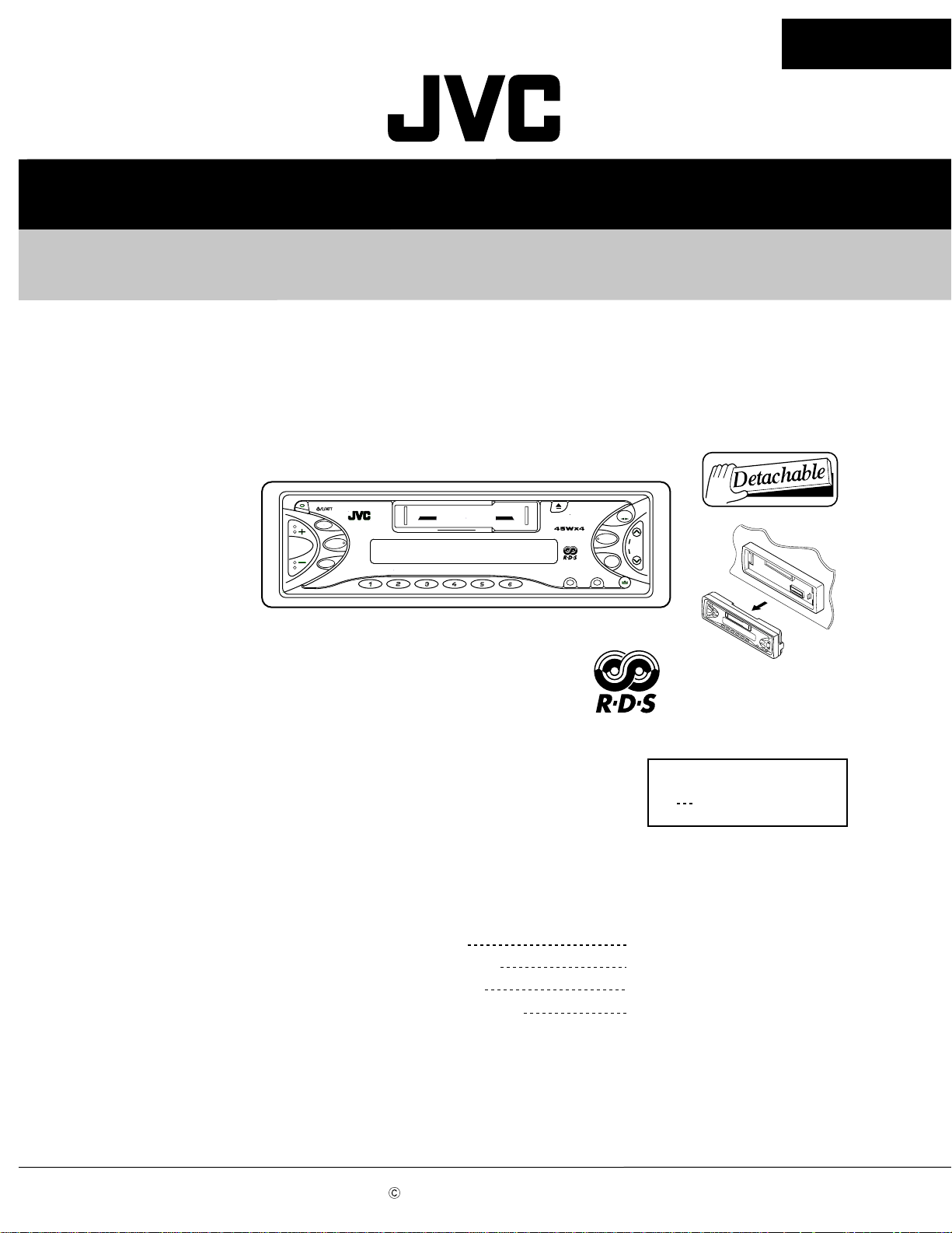
SERVICE MANUAL
CASSETTE RECEIVER
KS-FX772R
KS-FX772R
Contents
TP/PTY
SEL
DISP
7
CD CHANGER CONTROL
MO
8
10
9
11 12
RPT
Safety precaution
Disassembly method
Adjustment method
Description of major ICs
KS-FX772R
RND
MODE
TAP
E
DAB
FM/AM
¢
SSM
4
CDCH
SCM
Area Suffix
E Continental Europe
1-2
1-3
1-18
1-22
COPYRIGHT 2002 VICTOR COMPANY OF JAPAN, LTD.
No.49694
Mar. 2002
Page 2
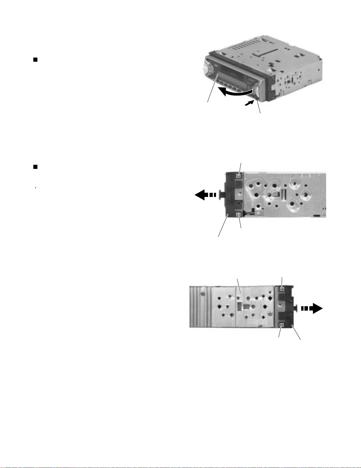
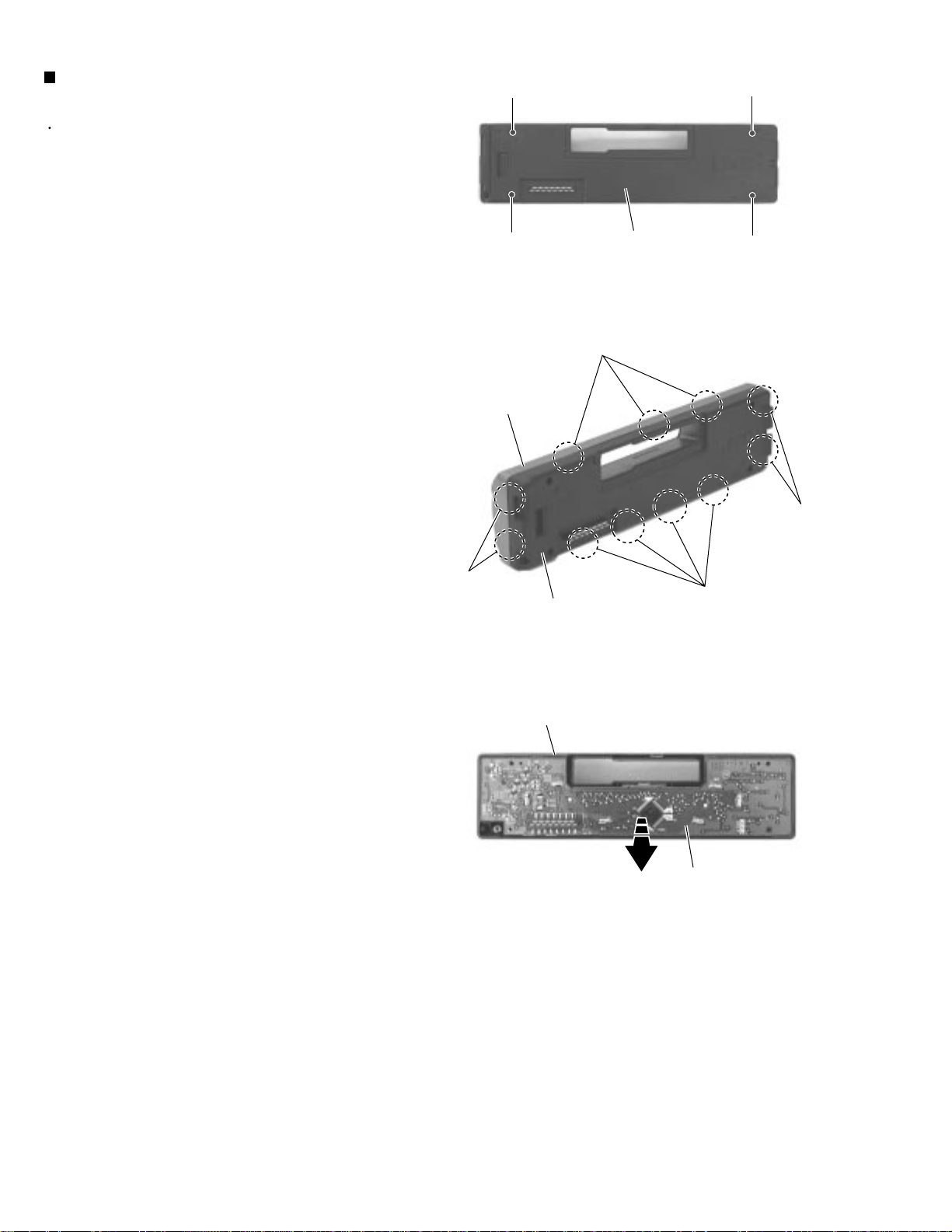
Disassembly method
<Main body>
Removing the front panel assembly
(See Fig.1)
1.
Press the eject button in the lower right part of the
front panel. Remove the front panel assembly from
the body.
Removing the front chassis assembly
(See Fig.2 , 3)
KS-FX772R
Front panel assembly
Eject button
Fig.1
Joint a
Prior to performing the following procedure, remove
the front panel assembly.
1.
Release the four joints a on both sides of the front
chassis assembly and remove the front chassis
assembly toward the front.
Joint a
Front chassis assembly
Heat sink
Fig.2
Joint a
Joint a
Front chassis
assembly
Fig.3
1-3
Page 3
KS-FX772R
Removing the heat sink (See Fig.4)
1.
Remove the three screws A on the left side of the
body.
Removing the bottom cover
(See Fig.5 , 6)
Prior to performing the following procedure, remove
the front panel assembly, the front chassis assembly
and the heat sink.
1.
Turn over the body and unjoint the five joints b with
the bottom cover and the body using a screwdriver.
A
Joint b
Joint b
Heat sink
Fig.4
Rear panel
Fig.5
A
Bottom cover
Joint b
Joint b
Bottom cover
Joint b
Joint b
Rear panel
Fig.6
1-4
Page 4
KS-FX772R
Removing the main board
(See Fig.7 , 8)
Prior to performing the following procedure, remove
the front panel assembly, the front chassis assembly,
the heat sink and the bottom cover.
1.
Remove the screw B, the three screws C and the
two screws D attaching the rear bracket on the back
of the body. Remove the rear panel.
2.
Remove the two screws E attaching the main board
on the bottom of the body. Disconnect connector
CN701 on the main board in the direction of the
arrow.
D
E
Rear panel
Fig.7
C
Main board
B
C
D
E
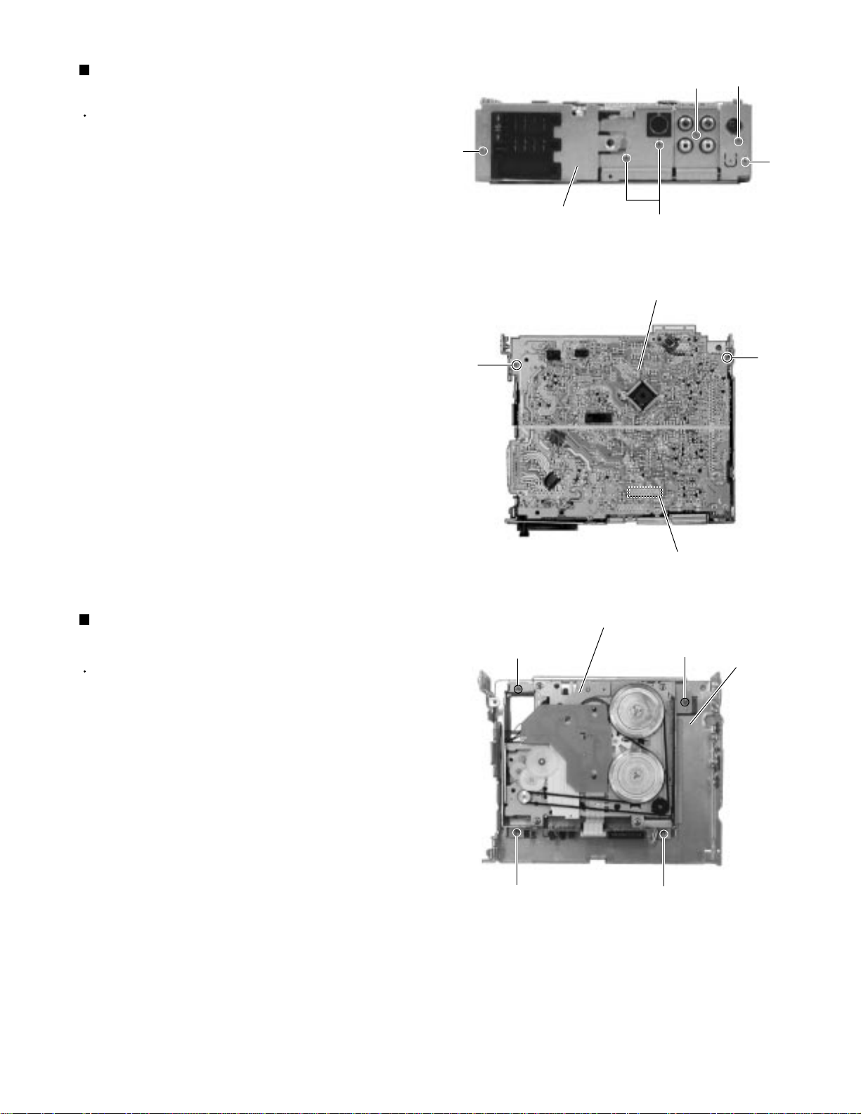
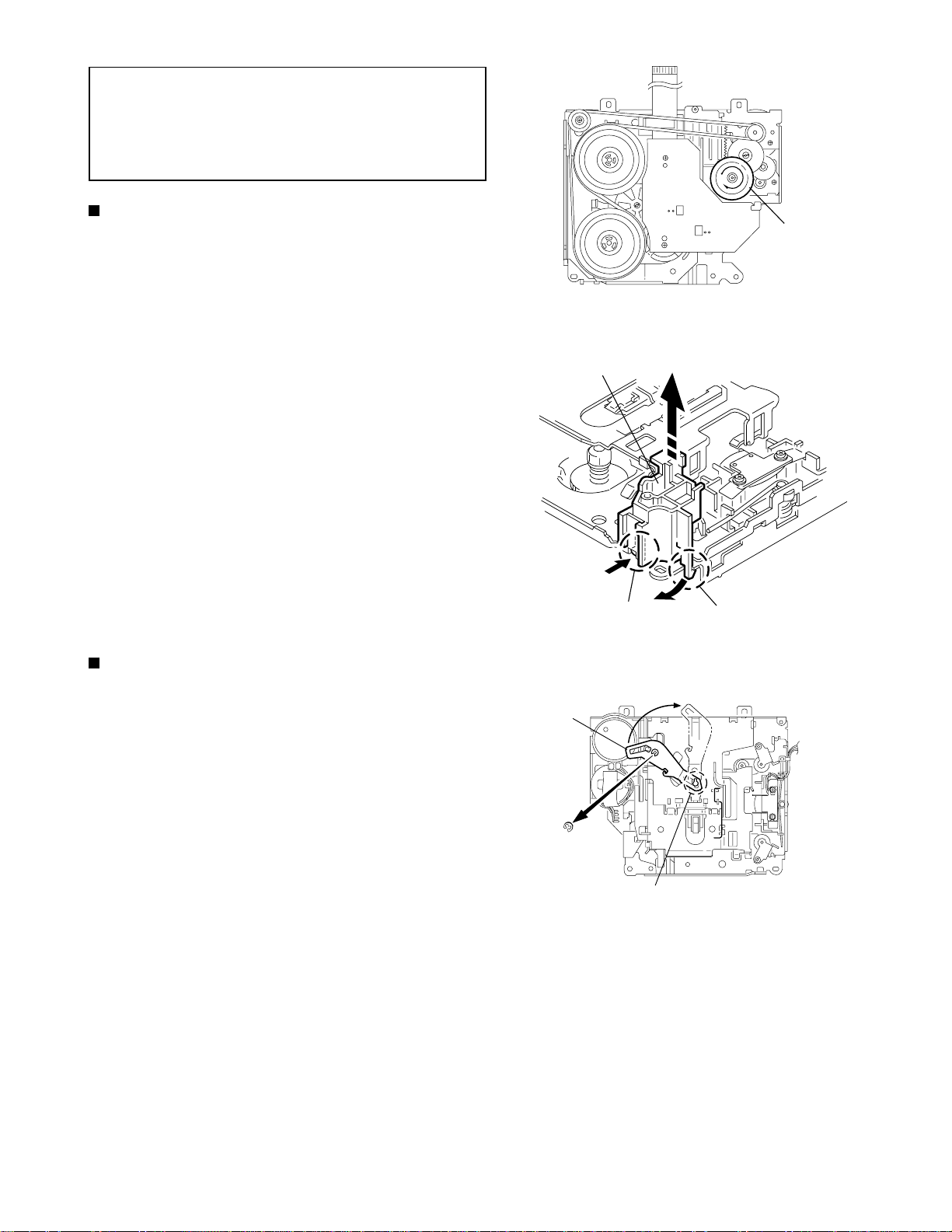
Removing the cassette mechanism section
(See Fig.9)
Prior to performing the following procedure, remove
the front panel assembly, the front chassis assembly,
the heat sink, the bottom cover and the main board.
1.
Remove the four screws F attaching the cassette
mechanism section on the back of the top chassis.
Fig.8
Cassette mechanism section
F
F
Fig.9
CN701
F
F
Top chassis
1-5
Page 5
KS-FX772R
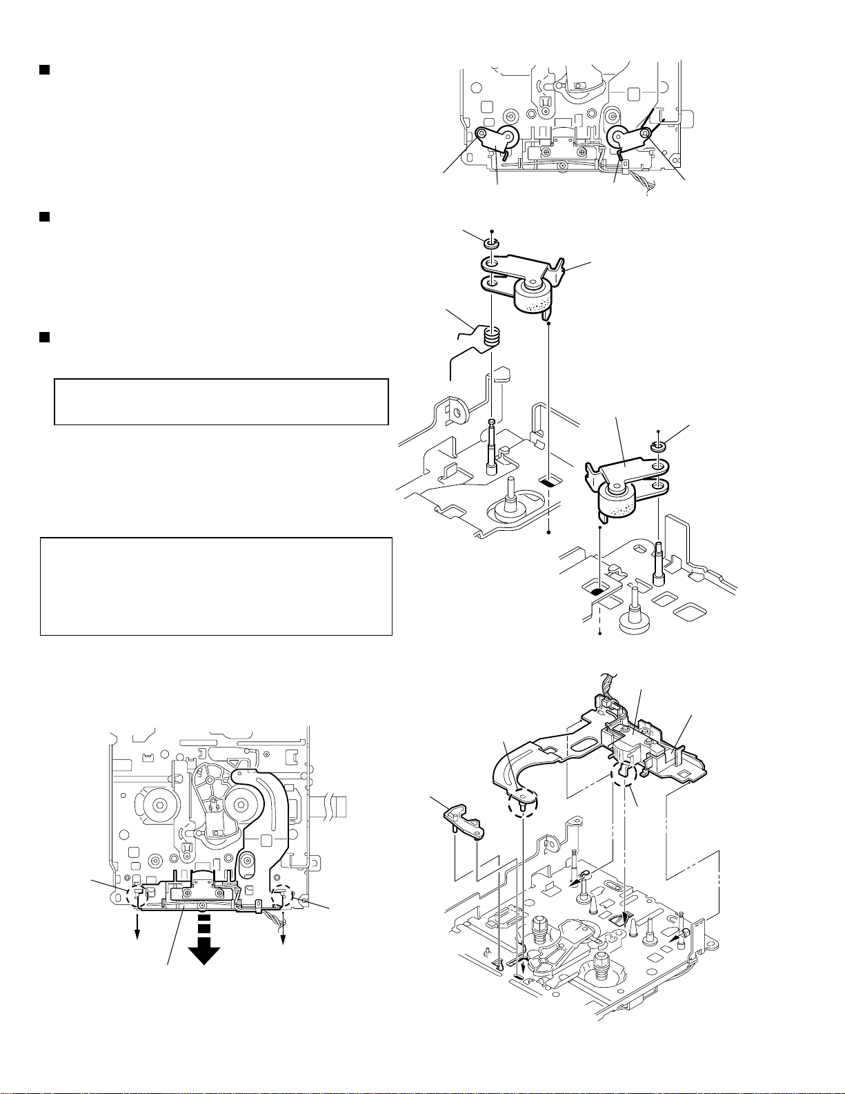
Removing the control switch board
(See Fig.10 ~ 12)
Prior to performing the following procedure, remove
the front panel assembly.
1.
Remove the four screws G attaching the rear cover
on the back of the front panel assembly.
2.
Unjoint the eleven joints c with the front panel and
the rear cover.
3.
Remove the control switch board on the back of the
front panel.
G
G
Front panel
Rear cover
Joint c
G
G
Fig.10
Joint c
Joint c
Rear cover
Front panel
Joint c
Fig.11
Control switch board
Fig.12
1-6
Page 6
KS-FX772R
REFERENCE:
Prior to performing the following
procedures, turn the mode gear on the
bottom of the body until the respective part
comes to the EJECT position (Refer to
Fig.1).
Removing the cassette guide (See Fig.2)
1.
Turn the mode gear to set to RVS play or
subsequent mode.
2.
Remove the cassette guide from the main chassis
while releasing each two joint tabs a in the direction
of the arrow.
Mode gear
Fig.1
Cassette guide
Removing the load arm (See Fig.3)
1.
Remove the E-washer attaching the load arm.
2.
Move the load arm in the direction of the arrow and
release the joint b on the cassette catch.
Load arm
E-washer
Tab a
Joint b
Tab a
Fig.2
Fig.3
1-7
Page 7
KS-FX772R
Removing the cassette hanger assembly /
cassette holder (See Fig.4 to 7)
1.
Check the mode is set to EJECT. Push down the
front part of the cassette holder and move in the
direction of the arrow to release the joint c.
2.
Move the rear part of the cassette hanger assembly
in the direction of the arrow to release it from the two
joint bosses d.
3.
Release the holder stabilizer spring from the hooks e
and f, then pull out from the cassette hanger
assembly.
4.
Bring up the rear side of the cassette hanger
assembly to release the joint g and h.
5.
Pull out the cassette catch from the cassette hanger
assembly.
Cassette holder assembly
Side bracket
Joints c
Cassette holder assembly
Cassette stabilizer spring
Fig.4
Boss d
Cassette hanger assembly
Cassette hanger
assembly
Boss d
Cassette holder
assembly
Hook g
Fig.6
Hook f
Hook e
Fig.5
Cassette hanger assembly
Cassette catch
Cassette holder assembly
Cassette hanger assembly
Hook h
Fig.7
1-8
Page 8
KS-FX772R
Removing the side bracket assembly
(See Fig.8 to 10)
1.
Remove the screw A attaching the side bracket
assembly.
2.
Detach the front side of the side bracket assembly
upward and pull out forward to release the joint i and
j in the rear.
CAUTION:
CAUTION:
When reassembling, make sure that the
boss k of the main chassis is set in the
notch of the load rack under the side
bracket assembly. Do not reattach the
load rack on the boss k.
After reattaching the side bracket
assembly, confirm operation.
Side bracket assembly
Joint i
Joint j
A
Side bracket assembly
Fig.8
Side bracket assembly
Joint i
Joint j
Load rack
Load rack
Boss k
Boss k
Fig.9
Fig.10
1-9
Page 9
KS-FX772R
Removing the pinch arm (F) assembly
(See Fig.11 and 12)
1.
Remove the polywasher and pull out the pinch arm
(F) assembly.
2.
Remove the compulsion spring.
Removing the pinch arm (R) assembly
(See Fig.11 and 13)
1.
Remove the polywasher and pull out the pinch arm
(R) assembly.
Removing the slide chassis assembly
(See Fig.14 and 15)
Polywasher
Pinch arm
(R) assembly
Polywasher
Compulsion spring
Fig.11
Pinch arm
(F) assembly
Pinch arm (F) assembly
Polywasher
REFERENCE:
It is not necessary to remove the head
and the tape guide.
1.
Move the slide chassis assembly in the direction of
the arrow to release the two joints l and remove from
the main chassis.
2.
Remove the rack link.
CAUTION:
When reassembling, first reattach the rack
link, and next fit the boss m and hook n of
the slide chassis assembly to the hole of
the main chassis, and engage the two joints
l.
Rack link
Fig.12
Boss m
Pinch arm
(R) assembly
Fig.13
Head
Hook n
Polywasher
Tape guide
Joint l
Slide chassis assembly
1-10
Fig.14
Joint l
Fig.15
Page 10
KS-FX772R
Removing the head / tape guide
(See Fig.16 and 17)
REFERENCE:
1.
Remove the band attaching the wire to the head.
2.
Remove the two screws B, the head and the head
support spring.
3.
Remove the pinch arm spring from the tape guide.
4.
Remove the tape guide and the pinch spring arm.
CAUTION:
CAUTION:
It is not necessary to remove the slide
chassis assembly.
When reattaching the pinch arm spring, set
both end of it to the pinch spring arm (
remarked o).
When reattaching the head, set the wires
into the groove of the tape guide (Fig.16).
B
Slide chassis assembly
Head
Tape guide
Fig.16
B
Pinch arm spring
Head
Head support spring
Tape guide
Removing the flywheel assembly (F) & (R)
(See Fig.18 and 19)
REFERENCE:
1.
Remove the belt at the bottom.
2.
Remove the two polywashers on the upper side.
3.
Pull out each flywheel assembly downward.
Flywheel assembly (F)
It is not necessary to remove the slide
chassis assembly.
Belt
o
Pinch spring arm
o
Slid chassis assembly
Fig.17
Polywasher
Polywasher
Flywheel assembly (R)
Fig.18
Flywheel assembly (F)
Fig.19
Flywheel assembly (R)
1-11
Page 11
KS-FX772R
Disassembling the flywheel assembly (F)
(See Fig.20 and 21)
1.
Push and turn counterclockwise the spring holder (F)
to release the three joints p on the bottom of the
flywheel.
2.
The spring holder (F), the TU spring and the friction
gear play come off.
3.
Remove the polywasher and felt.
Flywheel assembly (F)
Joints p
Flywheel assembly (R)
Joints q
Disassembling the flywheel assembly (R)
(See Fig.20 and 22)
1.
Push and turn clockwise the spring holder (R) to
release the three joints q on the bottom of the
flywheel.
2.
The spring holder (R), the FF spring and the friction
gear FF come off.
3.
Remove the polywasher and the felt.
Removing the reel board
(See Fig.23 and 24)
1.
Remove the two screws C attaching the reel board.
2.
Move the reel board in the direction of the arrow to
release the joint r.
3.
Unsolder the wires if necessary.
CAUTION:
When reattaching, confirm operation of
the MODE switch and the ST-BY switch.
The mode position between EJECT and
ST-BY is optimum for reattaching.
Joint p
Fig.20
Polywasher
Polywasher
Spring holder (R)
Spring holder (F)
TU spring
Friction gear FF
Friction gear play
Felt
Flywheel assembly (F)
FF spring
Felt
Flywheel assembly (R)
Fig.21 Fig.22
Joint q
1-12
Connect the card wire extending from
the reel board to the FFC pad before
reattaching the reel board.
FFC pad
C
Reel board
C
Fig.23
Joint r
FFC pad
CT-1 switch
MODE switch
Soldering
ST-BY switch
Fig.24
Page 12

KS-FX772R
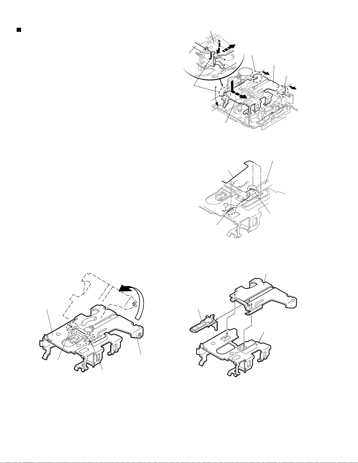
Removing the gear base arm / gear base
link assembly (See Fig.25 to 27)
1.
Move the gear base arm in the direction of the arrow.
2.
Insert a slotted screwdriver to the gear base spring
under the gear base arm, and release the gear base
arm upward from the boss on the gear base
assembly.
3.
Remove the gear base arm from the main chassis
while releasing the two joints s.
4.
Move the gear base link assemby in the direction of
the arrow to release the two joints t.
REFERENCE:
When reattaching the gear base arm,
make sure that the boss on the gear
base assembly is inside the gear base
spring.
Removing the FFC pad
(See Fig.27 and 29)
Gear base
link assembly
Gear base spring
Joint t
Gear base arm
Joints s
Hook u
FFC pad
Hook u
Joint t
Fig.25
Gear base arm
Screwdriver
1.
Push each joint hook u of the FFC pad and remove
toward the bottom.
Gear base link assembly
Fig.26
Gear base arm
Fig.27
FFC pad
1-13
Page 13

KS-FX772R
Removing the mode gear
(See Fig.28 and 31)
1.
Remove the polywasher on the bottom and pull out
the mode gear.
Removing the mode switch actuator
(See Fig.28, 29 and 31)
1.
Pull out the mode switch actuator at the bottom.
REFERENCE:
When reattaching the mode switch
actuator to the main chassis, make sure to
set on the shaft and insert v into the slot w.
Removing the direction link / direction
plate (See Fig.29 to 31)
1.
Remove the polywasher attaching the direction link.
2.
Bring up the direction link to release the three joints
x, y and z at a time.
3.
Move the direction plate in the direction of the arrow
to release the two joints a’.
REFERENCE:
When reattaching the direction plate,
engage the two joints a’ and move in the
direction of the arrow (Refer to Fig.30).
Mode switch actuator
Direction plate
Direction link
Fig.28
Direction plate
Joints a'
Joint z
Direction link
Slot w
Joint y
Polywasher
Fig.29
Direction plate Mode rack assembly
Joint b'
Mode gear
Polywasher
Mode rack assembly
Joint x
Joint b'
Joint c'
REFERENCE:
When reattaching the direction link,
move the direction plate in the direction
of the arrow and engage the three joint
x, y and z at a time (Refer to Fig.31).
Removing the mode rack assembly
(See Fig.29 and 30)
1.
Move the mode rack assembly in the direction of the
arrow to release the two joints b’ and the joint c’.
REFERENCE:
When reattaching, set the two b’ on the
bottom of the mode rack assembly into the
slots of the main chassis and move in the
direction of the arrow (See Fig.30).
Joints a'
Fig.30
Direction link
Mode switch actuator
Polywasher
v
Mode gear
Direction plate
Mode rack assembly
Fig.31
1-14
Page 14

KS-FX772R
Removing the gear base assembly / take
up gear / reflector gear (See Fig.32 to 34)
1.
Push in the pin d’ of the gear base assembly on the
upper side of the body and move the reflector gear
toward the bottom, then pull out.
2.
Remove the polywasher on the bottom and pull out
the take up gear.
3.
Move the gear base assembly in the direction of the
arrow to release it from the two slots e’ of the main
chassis.
REFERENCE:
The parts are damaged when removed.
Please replace with new ones.
Gear base assembly
Pin d'
Polywasher
Slot e'
Slot e'
Fig.32
Take up gear
Removing the reel driver / reel spindle
(See Fig.34)
1.
Draw out the reel driver from the shaft on the main
chassis and remove the reel driver spring and the
reel spindle respectively.
CAUTION:
The reel driver is damaged when
removed. Please replace with a new
one.
Reflector gear
Reel driver
Reel driver spring
Reel spindle
Main chassis
Fig.33
Reel driver
Reel driver spring
Reel spindle
Gear base assembly
Slots e’
Take up gear
Reflector gear
Polywasher
Fig.34
1-15
Page 15

KS-FX772R
Removing the side bracket assembly
(See Fig.35 to 39)
1.
Remove the eject cam plate spring.
2.
Push the joint f‘ through the slot to remove the load
rack downward.
3.
Move the eject cam limiter in the direction of the
arrow to release it from the boss g’ of the side
bracket assembly and from the two joints h’.
4.
Move the eject cam plate in the direction of the arrow
to release the joint i’.
Joint f'
CAUTION:
Joint h'
When reassembling, confirm operation of
each part before reattaching the eject cam
plate spring.
Side bracket assembly
Boss g'
Eject cam limiter
Side bracket assembly
Joint h'
Joint f'
Eject cam plate spring
Joint h'
Load rack
Fig.35
Boss g'
Eject cam limiter
Eject cam plate
Fig.37
Joint h'
1-16
Fig.36
Side bracket assembly
Boss g'
Eject cam plate
Fig.38
Load rack
Joint i'
Side bracket assembly
Eject cam plate
Joint i'
Fig.39
Page 16

KS-FX772R
Removing the main motor assembly /
sub motor assembly (See Fig.40 to 42)
1.
Remove the belt at the bottom.
2.
Remove the polywasher and pull out the mode gear.
3.
Pull out the reduction gear (B).
4.
Remove the polywasher and pull out the reduction
gear (A).
5.
Remove the two screws D attaching the main motor
assembly.
6.
Remove the two screws E attaching the sub motor
assembly.
7.
Unsolder the wires on the reel board if necessary.
CAUTION:
When reassembling, adjust the length of the
wires extending from the sub motor
asswmbly by attaching them to the side of
the sub motor assembly with the wires
extending from the main motor assembly
using a spacer.
Belt
Reduction gear (B)
Reduction gear (B)
E
Polywasher
Fig.40
D
E
Mode gear
Polywasher
Reduction gear (A)
D
Main motor
assembly
Reduction
gear (A)
Polywasher
Sub motor
assembly
Spacer
Main motor assembly
Sub motor assembly
Main motor assembly
Sub motor assembly
Fig.41
Spacer
Fig.42
1-17
Page 17

KS-FX772R
Adjustment method
Test Instruments reqired for adjustment
1.Digital osclloscope(100MHz)
2.Frequency Counter meter
3.Electric voltmeter
4.Wow & flutter meter
5.Test Tapes
VT724
VT739
VT712
VT703
6.Torque gauge
Measuring conditions(Amplifier section)
Power supply voltage
Load impedance
Line out level / Impedance
For playback frequency measurement
For wow flutter & tape speed measurement
for DOLBY level measurement
For head azimuth measurement
Cassette type for CTG-N
(mechanism adjustment)
DC14.4V(11V to 16V allowance)
4 (4 to 8 allowance)
Tuner area
Band range
FM : 87.5MHz to 108.0MHz
AM : (MW) 522kHz to 1620 kHz
(LW) 144kHz to 279 kHz
DUMMY LOAD
Exclusive dummy load should be used for AM
and FM dummy load,there is a loss of 6dB
between SSG output and antenna input. The
loss of 6dB need not be considered since
direct reading of figures are applied in this
working standard.
2.0V / 20k
1-18
Page 18

Arrangement of adjusting & test points
Cassette mechanism
(Surface)
Motor assembly
KS-FX772R
Tape speed adjust
Head section view
Azimuth screw A
(Forward)
Playback head
Azimuth screw B
(Reverse)
Azimuth screw B
(Reverse)
Azimuth screw A
(Forward)
Playback Head
1-19
Page 19

KS-FX772R
Arrangment of adjusting
Head amplifier board section (Reverse side)
R411
VR402
FSMW1093A
B409
R426
C423
R425
D401
1
T11
R424
IC402
VR402:Rch
(Dolby NR level
B407
C425
C424
Q401
R410
B406
D402
R401
R416
C419
C422
C413
C414
B408
C421
adj)
C418
R420
Q403
R412
11
R414
R415
R418
B411
B410
21
R413
R417
C417
B404
CJ403
2
C415
1
B413
C416
B403
(Dolby NR F
C412
1
IC401
31
C411
B405
B412
VR401
B402
R423
requency response adj)
B401
R408
C410
C409
R405
R406
C405
C406
R407
C407
C403
C408
R403
R402
C402
2
CJ401
1
C404
R404
C401
1
R422
Q402
VR401:Rch
Information for using a car audio service jig
1. We're advancing efforts to make our extension cords common for all car audio products.
Please use this type of extension cord as follows.
2. As a U-shape type top cover is employed, this type of extension cord is needed to check operation of the
mechanism assembly after disassembly.
3. Extension cord : EXTKSRT002-18P ( 18 pin extension cord ) For connection between mechanism assembly
and main board assembly .
Check for mechanism driving section such as motor ,etc..
Cassette mechanism
Disassembly method
1. Remove the bottom cover.
2. Remove the front panel assembly.
3. Remove the top cover .
4. Install the front panel.
5. Confirm that current is being carried by connecting
an extension cord jig.
Note
Available to connect to the CP701 connector when installing the front panel.
Extension cord
EXTKSRT002-18P
to Cassette mechanism
1-20
EXTKSRT002-18P
Main board
to Main board
Front panel assembly
Page 20

KS-FX772R
Item
Head
1.
azimuth
adjustment
Conditions
Test tape:
SCC-1659
VT703(10kHz)
Adjustment and Confirmation methods
Head height adjustment
Adjust the azimuth directly. When you
adjust the height using a mirror tape,
remove the cassette housing from the
mechanism chassis. After installing the
cassette housing, perform the azimuth
adjustment.
Load the SCC-1659 mirror tape. Adjust with
1.
height adjustment screw A and azimuth
adjustment screw B so that line A of the
mirror tape runs in the center between Lch
and Rch in the reverse play mode.
After switching from REV to FWD then to
2.
REV, check that the head position set in
procedure 1 is not changed. (If the position
has shifted, adjust again and check.)
Adjust with azimuth adjustment screw B so
3.
that line B of the mirror tape runs in the
center between Lch and Rch in the forward
play mode.
Head azimuth adjustment
Load VT724 (1kHz) and play it back in
1.
the reverse play mode.
Set the Rch output level to max.
Load VT703 (10kHz) and play it back in
2.
the forward play mode. Adjust the Rch
and Lch output levels to max, with
azimuth adjustment screw B. In this case,
the phase difference should be within 45 .
Engage the reverse mode and adjust the
3.
output level to max, with azimuth
adjustment screw C.
(The phase difference should be 45 or
more.)
When switching between forward and
4.
reverse modes, the difference between
channels should be within 3dB. (Between
FWD L and R, REV L and R.)
S.Values Adjust
A line
Head shield
The head is at low position
during.
B line
Head shield
The head is at High position
during REV.
Output
level:
Maximum
PBHead
FWD Adj B
REV Adj C
(0 ) (45 )
HEIGHT Adj A
phase
Tape speed
2.
and wow
flutter
confirmation
Play back
3.
frequency
response
confiramation
When VT721 (315Hz) is played back,
5.
the level difference between channels
should be within 1.5dB.
Test tape: VT712
(3kHz)
Test tape: VT724
(1kHz)
VT739
(63Hz / 1kHz / 10kHz)
The tuner section is of an adjustment-freedesign. In case the tuner is in trouble, replace the tuner pack.
Check to see if the reading of the F, counter /
1.
wow flutter meter is within 3015 3045(FWD
/ REV), and less than 0.35% (JIS RMS).
In case of out of specification, adjust the
2.
motor with a built-in volume resistor.
Play test tape VT724, and set the volume
1.
position at 2V.
Play test tape VT739 and confirm.
2.
1kHz / 10kHz: -1 3dB,
1kHz / 63Hz: 0 3dB,
When 10kHz is out of specification, it will be
3.
necessary to read adjust the azimuth.
Tape speed:
3015
3045Hz
Wow
flutter: less
than 0.35%
Speaker out
1kHz / 63Hz
: 0 3db
1kHz / 10kHz
: -1 3db
Built-in volume
resistor
1-21
Page 21

KS-FX772R
Description of major ICs
HA13164A(IC901):Regulator
1.Terminal layout
2.Block diagram
3.Pin function
11
12
10
8
2
1
7
Surge Protector
BIAS TSD
15
3
TAB
note1) TAB (header of IC)
connected to GND
13
9
6
4
5
14
UNIT R:
C:F
1-22
Pin No. Symbol Function
1
2
EXT
ANTOUT
Output voltage is VCC-1 V when M or H level applied to CTRL pin.
Output voltage is VCC-1 V when M or H level to CTRL pin and H level
to ANT-CTRL.
3
4
5
6
7
8
9
10
11
12
13
14
15
ACC-IN
5.6V
SW5V
ACC-HOL
ANTCTP
MEMORY
MEMDET
9V
PWR-CNI
8V
ILL 10V
IILL-ADJ
GND
Connected to ACC.
Regular 5.6V.
Output voltage is 5V when M or H level applied to CTRL pin.
Output for ACC detector.
L:ANT output OFF , H:ANT output ON
Connected to VCC.
Low battery detect.
Output voltage is 9V when M or H level applied to CTRL pin.
L:BIAS OFF, M:BIAS ON, H:CD ON
Output voltage is 8V when H level applied to CTRL pin.
Adjustment pin for ILM output voltage.
Output voltage is 10V when M or H level applied to CTRL pin.
Connected to GND.
Page 22

CXA2559Q(IC401):Playback equalizer amplifier with music sensor
30
29
28
27
26
LPF
5
25
BIAS
MUTE
TAPE EQ
FWD/RVS
6
1.Pin layout
3.Pin function
1
10
30
21
2.Blockdiagram
31
32
33
34
35
36
37
38
39
40
45k
7k/12k
300k
300k
7k/12k
1
30k
30k
100k
+
F2
F1
+
-
2
T2
X1
X1
T1
100k
3
4
Vcc
F3
KS-FX772R
24
23
22
21
24dB
-
+
MS MODE
+
-
+
DET
-
24dB
7
8
9
MS ON/
OFF
10
20
19
18
17
16
15
14
13
12
11
Pin No.
1
2
3
4
5
6
7
8
9
10
11
12
13
14
15
16
17
18
19
20
21
22
23
24
25
26
27
28
29
30
31
32
33
34
35
36
37
38
39
40
Symbol
PBTC1
PBOUT1
OUTREF1
TAPEIN1
Vcc
NC
LINEOUT1
TCH1
NC
MSLPF
G2FB
G1FB
MSTC
MSOUT
NC
NRSW
MUTE
METAL
DIRECTION
FF/REW
MSSW
NC
TCH2
OUT2
DIREF
GND
TAPEIN2
OUTREF2
PBOUT2
PBTC2
PBFB2
PBRIN2
PBGND
PBFIN2
VCT
PBREF
PBFIN1
PBGND
PBRIN1
PBFB1
I/O
Function
-
Terminal of capacity of reproduction equalizer reproduction
O
Equalizer output terminal
O
Output standard terminal
I
Tape input terminal
-
Power supply terminal
-
Non connection
O
Line-out output terminal
-
Time constant for the HLS
-
Non connected
-
Detection LPF terminal between tunes
-
Detection level set terminal between tunes
-
Detection level set terminal between tunes
-
Time constant connection terminal for the detection between tunes
O
Detection output terminal between tunes
-
Non connected
I
Dolby NR control
I
Mute function control terminal
I
Reproduction equalizer control terminal
I
Head change control terminal
I
Detection mode control terminal between tunes
I
Detection function control terminal between tunes
-
Non connected
-
Time constant for the HLS
O
Line-out output terminal
-
Resistance connection terminal for standard current setting
-
Earth terminal
I
Tape input terminal
O
Output standard terminal
O
Reproduction equalizer output terminal
-
Terminal of capacity of reproduction equalizer
I
Reproduction equalizer return terminal
I
Reproduction equalizer input terminal
-
Reproduction equalizer system earth terminal
I
Reproduction equalizer input terminal
O
Middle point terminal
O
Reproduction equalizer standard terminal
I
Reproduction equalizer input terminal
-
Reproduction equalizer system earth terminal
I
Reproduction equalizer input terminal
I
Reproduction equalizer return terminal
1-23
Page 23

KS-FX772R
UPD178018AGC625(IC701) : Main system control CPU
1. Pin layout
2. Pin function
Pin No.
1
2
3
4
5
6
7
8
9
10
11
12
13
14
15
16
17
18
19
20
21
22
23
24
25
26
27
28
29
30
31
32
33
34
35
36
37
38
39
40
80 ~ 61
1
~
20
21 ~ 40
60
~
41
Port Name I/O Descriptions
KEY 0
KEY 1
KEY 2
LEVEL
SM
SQ
LCDCE
LCDDA
LCDSCK
BUSI/O
OPEN
BUSSI
BUSSO
BUSSCK
NC
NC
NC
NC
INLOCK
NC
GNDPORT
VDDPORT
NC
AFCK
MONO
FM/AM
SEEK/STOP
NC
IFC
VDDPLL
FMOSC
NC
GNDPLL
AMEO
FMEO
IC
SD/ST
STAGE0
NC
MOTOR
I
I
I
I
I
I
O
O
O
I
I
I
O
I/O
-
-
-
-
-
-
-
O
O
O
O
O
I
I
-
I
-
O
O
-
I
I
O
Key input 0
Key input 1
Key input 2
Level meter input
S.meter level input
S.Quality level input
CE output to LCD driver
Data output to LCD driver
Clock output to LCD driver
I/O selector output for J-BUS, H : OUT, L: INPUT
Door open detect input
J-BUS Data input
J-BUS Data output
J-BUS Clock in/output
Non connect
Non connect
Non connect
Non connect
Non connect
Non connect
Port GND
Port Vdd
Non connect
AF check output, L: AF check
Monaural on /off selecting output, H:mono on
FM/AM switching output L : FM H : AM
Auto seek /stop selecting output, H: Seek, L:Stop
Pulse signal input port for Cruise control
FM/AM midle frequency counter input
PLL Vdd
FM/AM limited generator frequency input
None connect
PLL GND
AM error out output
FM error out output
GND
Station detector, Stereo signal input, H:Find Station, L:Stereo
Pull up
Non connect
Main motor output
1-24
Page 24

Pin No.
41
42
43
44
45
46
47
48
49
50
51
52
53
54
55
56
57
58
59
60
61
62
63
64
65
66
67
68
69
70
71
72
73
74
75
76
77
78
79
80
Port Name I/O Descriptions
FF/REW
F/R
DOLBY
MSIN
I2CSCK
I2CDAO
I2CDAI
REEL
SUBMO1
SUBMO2
MODE
TAPEIN
STANDBY
NC
NC
NC
NC
NC
NC
MUTE
PCNT
TELMUTE
NC
NC
LEDB
LEDR
ACCDET
POWER
RDSSCK
RDSDA
REMOCON
DETACH
J-BUSINT
REGCPU
GND
X2
X1
REGOSC
VDD
RESET
I
O
O
I
O
O
I
O
I
O
O
O
I
-
-
-
-
-
O
O
I
O
O
O
I
O
I
I
I
I
I
-
-
-
I
-
-
-
Output for input signal lev el s witching f or MS L : FF,REW H : PLAY
FWD,REV running direction s witch signal input
Dolby on "H" output
MS input
I2C information clock output
I2C information data output
I2C information clock input
Switch for detecting tape end position
Sub motor clock direction input
Sub motor clock opposite detection drive output
Mechanism mode position detection input
Cassette in detection input H : cassette in L : cassette out
Standby position detection input H : eject side L : operation side
Non connect
Non connect
Non connect
Non connect
Non connect
Non connect
Mute output , L : mute on
Power ON /OFF switching output , H : power on
Telephone mute signal detection input
Non connect
Non connect
LED color control
LED color control
Power sa v e 1 Working togethe ACC Power save : L
Power sa v e 2, Working together Back up by H input, stop mode
Clock input for RDS
RDS data input
Remocom input
Detach signal input H : Power save
Cut-in input for J-BUS signal
Regulator for CPU power supply, Connect the GND with0.1 F.
Ground
Connecting the crystal oscillator for system clock
Connecting the crystal oscillator for system clock
Regulator for oscillator circuit.Connect the GND with 0.1 F.
Vdd
Pull up
KS-FX772R
UPD178018AGC625(2/2)
1-25
Page 25

KS-FX772R
LA4743K(IC301):Power AMP
1.Block diagram
IN 1
TAB
IN 2
+
0.22 F
+
0.22 F
11
1
12
Vcc 1/2 Vcc 3/4
6 20
-
+
Protective
circuit
-
+
2200 F 0.022 F
+
9
-
7
+
OUT 1+
OUT 1-
PWR GND1
8
+
OUT 2+
5
-
OUT 2-
3
PWR GND2
2
ST BY
R.F
47 F
IN 3
PRE GND
IN 4
+5V
ST ON
+
0.22 F
N.C
+
0.22 F
4
Stand by
Switch
Mute
3.3 F
OUT 3+
OUT 3-
10K
+
Low Level
Mute ON
10
+
Ripple
Filter
Mute
22
circuit
+
15
-
+
-
17
19
25
18
21
23
PWR GND3
OUT 4+
OUT 4-
13
14
Protective
circuit
-
+
+
-
1-26
ON TIME C
22 F
Muting &
16
+
ON Time Control
Circuit
PWR GND4
24
Page 26

2.Terminal layout
KS-FX772R
3.Pin function
1
2
3
4
5
6
7
8
9
10
11
12
13
14
15
16
17
18
19
20
21
22
23
24
25
SymbolPin No. Function
GND
GND
RROUTSTANDBY
RROUT+
VCC
FROUTGND
FROUT+
RIPPLE
FRIN
RRIN
SGND
RLIN
FLIN
ONTIME
FLOUT+
GND
FLOUTVCC
RLOUT+
MUTE
RLOUTGND
NC
Header of IC
Power GND
Outpur(-) for front Rch
Stand by input
Output (+) for front Rch
Power input
Output (-) for rear Rch
Power GND
Output (+) for rear Rch
Ripple filter
Rear Rch input
Front Rch input
Signal GND
Rear Lch input
Front Lch input
Power on time control
Output (+) for rear Lch
Power GND
Output (-) for rear Lch
Power input
Output (+) for front Lch
Muting control input
Output (-) for front Lch
Power GND
No connection
LA4743K
1-27
Page 27

KS-FX772R
LC75823W (IC651) : LCD driver
1. Pin Layout & Symbol
S50
S51
COM1
COM2
COM3
INH
OSC
CE
CLOCK
DATA
S49
S52
S48
S47
S46
S45
S44
S43
S42
S41
S40
S39
S38
S37
S36
S35
S34
S33
S32
S31
S30
S29
S28
S27
S26
S25
S24
S23
S22
S21
S20
S19
S18
S17
S6
S7
S5
S3
S4
S11
S12
S13
S10
S9
S8
2. Pin Function
Pin No. Symbol I/O Function
1 to 2
3 to 52
NC
S1 to S52
--
Non connected
O
Segment output pins used to display data transferred
by serial data input.
53 to 55
COM1 to COM3
O
Common driver output pins. The frame frequency is given
by : t0=(fosc/384)Hz.
56
VDD
--
Power supply connection. Provide a voltage of between
4.5 and 6.0V.
57
INH
I
Display turning off input pin.
INT="L" (Vss) ----- off (S1 to S52, COM1 to COM3="L"
INT="H" (VDD)----- on
Serial data can be transferred in display off mode.
58~60
61
NC
OSC
--
Non connected
I/O
Oscillator connection.
An oscillator circuit is formed by connecting an external
resistor and capacitor at this pin.
62
CE
Serial data CE : Chip enable
interface connection
63
CLOCK
I
to the controller. CLOCK : Sync clock
S14
S15
S16
1-28
64
DATA
DATA : Transfer data
Page 28

SAA6579T-X(IC71):RDS
1.Pin layout
1
DATA
2
Vref
3
MUX
4
dd
V
5
GND
6
CIN
7
SCOUT
8
2.Block diagram
KS-FX772R
CLK
16
15
OSCO
14
OSCI
13
Vdd
12
GND
11
TEST
10
MODE
9
121413
3.Pin function
4
8
7
CLOCKED
COMPARATOR
5
3
REFERENCE
VOLT AGE
Pin No.
1
2
3
4
ANTIALIASING
FILTER
6 11
Symbol
VP1
57 kHz
BANDPASS
(8th ORDER)
COSTAS LOOP
VARIABLE AND
FIXED DIVIDER
CLOCK
REGERATION
AND SYNC
RECONSTRUCTION
FILTER
TEST LOGIC AND OUTPUT
SELECTOR SWITCH
Description
OSCILATOR
AND
DIVIDER
BIPHASE
SYMBOL
DECODER
910
Non connected
DATA
Vref
MUX
RDS data output
Reference voltage output (0.5VDDA)
Multiolex signal input
QUALITY BIT
GENERATOR
DIFFERENTIAL
DECODER
1
2
15
15
10
11
12
13
14
15
16
5
6
7
8
9
Vdd
GND
CIN
SCOUT
MODE
TEST
GND
Vdd
OSCI
OSCO
+5V supply voltage for analog part
Ground for analog part (0V)
Subcarrier input to comparator
Subcarrier output of reconstruction filter
Oscllator mode / test control input
Test enable input
Ground for digital part (0V)
+5V supply voltage for digital part
Oscillator input
Oscillator output
Non connected
CLK
RDS clock output
1-29
Page 29

KS-FX772R
TEA6320T-X (IC161) : E.volume
1.Pin layout
2.Block diagram
10 8 9 7 6
5
12
SDA
1
GND
2
OUTRL
OUTFL
MUTE
TL
B2L
B1L
IVL
ILL
QSL
IDL
ICL
IMD
IBL
IAL
3
4
5
6
7
8
9
10
11
12
13
14
15
16
3.Pin functions
Pin
Symbol
No.
SDA
1
SCL
32
VCC
31
OUTRR
30
OUTFR
29
TR
28
B2R
27
B1R
26
IVR
25
ILR
24
QSR
23
IDR
22
Vref
21
ICR
CD-CH
TAPE
TUNER
20
19
18
17
CAP
IBR
IAR
I/O
Serial data input/output.
I/O
MUTE
21
31
2
19
16
15
13
11
14
22
20
18
17
Functions Functions
POWER
SUPPLY
SOURCE
SELECTOR
23 25 24 26 27 28
VOLUME 1
+20 to -31 dB
LOUDNESS
LEFT
VOLUME 1
+20 to -31 dB
LOUDNESS
RIGHT
Pin
No.
17
Symbol
IAR
BASS
LEFT
+15 dB
LOGIC
BASS
RIGHT
+15 dB
I/O
I
Input A right source.
TREBLE
LEFT
+12 dB
TREBLE
RIGHT
+12 dB
FUNCTION
ZERO CROSS
DETECTOR
VOLUME 2
0 to 55 dB
BALANCE
FENDER REAR
VOLUME 2
0 to 55 dB
BALANCE
FENDER FRONT
HC BUS
REC
VOLUME 2
0 to -55dB
BALANCE
FENDER FRONT
VOLUME 2
0 to -55dB
BALANCE
FENDER REAR
3
4
32
1
29
30
2
3
4
5
6
7
8
9
10
11
12
13
14
15
16
GND
OUTRL
OUTFL
TL
B2L
B1L
IVL
ILL
QSL
IDL
MUTE
ICL
IMO
IBL
IAL
Ground.
output left rear.
O
output left front.
O
Treble control capacitor left channel or
I
input from an external equalizer.
Bass control capacitor left channel or
-
output to an external equalizer.
Bass control capacitor left channel.
Input volume 1. left control part.
I
Input loudness. left control part.
I
Output source selector. left channel.
O
Not used
Not used
Input C left source.
I
Not used
Input B left source.
I
Input A left source.
I
18
19
20
21
22
23
24
25
26
27
28
29
30
31
32
IBR
CAP
ICR
Vref
IDR
QSR
ILR
IVR
B1R
B2R
TR
OUTFR
OUTRR
Vcc
SCL
I
Input B right source.
-
Electronic filtering for supply.
I
Input C right source.
-
Reference voltage (0.5Vcc)
-
Not used
O
Output source selector right channel.
I
Input loudness right channel.
I
Input volume 1. right control part.
-
Bass control capacitor right channel
Bass control capacitor right channel or
O
output to an external equalizer.
Treble control capacitor right channel or
I
input from an external equalizer.
O
Output right front.
O
Output right rear.
-
Supply voltage.
I
Serial clock input.
1-30
Page 30

HD74HC126FP-X (IC801) : Buffer
KS-FX772R
1.Terminal layout
1C
1
1A
2
1Y
3
2C
4
2A
5
2Y
6
GND
7
2.Block diagram
Input
VU
14
4C
13
4A
12
4Y
11
3C
10
3A
9
3Y
8
Vcc Vcc
1A
2A
3A
4A
1C
2C
3C
See Function Table
4C
3.Pin function
Output
1Y
2Y
Output
2Y
Output
3Y
Output
4Y
Input
C
L
H
H
A
X
L
H
Output
Y
Z
H
L
Note) H:High level
L:Low level
X:Irrelevant
Z:Off(High-impedance)
State a 3-state input
1k
S1
CL
1k
Sample as Load Circuit 1
Sample as Load Circuit 1
Sample as Load Circuit 1
LB1641 (IC402) : DC motor driver
1. Pin layout
1 2 3 4 5 6 7 8 9
GNDOUT1 P1
VZ IN1 IN2
VCC1
VCC2 P2
Note) CL includes probe and jig capacitance
2. Pin function
Input Output
IN1 IN2 OUT1 OUT2
0 0 0 0
10
OUT2
1 0 1 0
0 1 0 1
1 1 0 0
Mode
Brake
CLOCKWISE
COUNTER-CLOCKWISE
Brake
1-31
Page 31

1
2
3
4
5
KS-FX772R
Block diagram
SUB
MOTOR
ABC
TO CD CHANGER
J801 CP901
SCK
SI/SO
IC801
CHANGER CONTROL
JBUS SI
JBUS SO
JBUS I/O
J1
AM
FM
AM/FM TUNER P ACK
Tuner.Power AMP.Changer/System Controller
JBUS SCK
TU1
CD RCH
CD LCH
SEEK/STOP
SD/ST
SMETER
TO SPEAKER
CONNECTOR TO REAR LINE OUT
L/R F
L/R R
IC301
POWER AMP
.
OUT LR
OUT RR
OUT LF
OUT RF
IC161
E.VOLUME
TUNER L/R
TAPE L/R
IC701
SYSTEM CONTROL MICON
LRO
RRO
SWITCH
TAPE END.STANDBY
J321
F/R
MODE
STANDBY
FF/REW
MOTOR
SUB02,01
TAPE IN
DOLBY
MS
REEL
KEY 0 – 2
CP401
CJ601
CJ403
CJ401
CP701
MAIN
MOTOR
MOTOR
TAPE IN
MODE
STANDBY
PHOTO
REEL
DOLBY
F/R
MS OUT
LCH
RCH
FF/REW
CE
CLOCK
DATA
HEAD
CJ402
LCH
RCH
IC401
PB EQ
IC402
DC MOTOR DRIVER
SUBMO+
SUBMO-
MECHANISM CONTROL
LCD1
QLD0158-001
S3 – S52
COM0 – COM3
IC651
LCD DRIVER
KEY
– S620
S601
LCD DRIVER/KEY SWITCH CIRCUT
2-1
Page 32

Standard schematic diagrams
Receiver & System control section
TU1
QAU0259-001
5
J1
QNB0100-002
L1
4.7u
D5
D6
1SS133-T2
1SS133-T2
C43
C33
150P
1k
R34
R44
R33
1k
R32
3.9k
C31
0.012
2SC3661-X
R748
2SC3661-X
Q31
68k
Q32
Q701
2SC2412K/R/-X
4
R43
10k
C32
R42
1k
0.058
C41
0.001
2SC2412K/R/-X
Q42
1k
Q41
R31
2SC2412K/R/-X
SW5V
10V
STANDBY
TAPEIN
MODE
SUB02
SUB01
3
REEL
MS
DOLBY
FR
FFREW
D705
UDZS5.6-X
D706
UDZS5.6-X
R706
R701
R702
R703
D707
UDZS5.6-X
R704
R705
D708
UDZS5.6-X
MOTOR
270
270
270
R751
R752
D709
UDZS5.6-X
10k
DETACH
KEY0
KEY1
KEY2
LCDCE
LCDCK
LCDDA
150k
LEDB
150k
LEDR
10k
10k
C717
0.047
CP401
QGB1214J1-18S
2
CJ601
VMC0334-001
D701
UDZS5.6-X
D702
UDZS5.6-X
D703
UDZS5.6-X
D704
UDZS5.6-X
1
J801
QNZ0095-001
0.47/50
1k
C42
2.2/50
FMEO
9V
CH.R
CH.L
C803
C802
120p
2SA1037AK/RS/-X
R2
1.5k
Q1
R41
DTC114EKA-X
C1
100/16
D1
MTZJ9.1C-T2
R1
33
10V
AMEO
FM/AM
C77
47/16
C76
0.01
C75
47p
R73
X71
2.2k
QAX0263-001Z
C74
82p
R59
470
47u
C55
0.47/50
L2
R750
47K
R807
100k
R808
100k
R809
100
330k
R810
47p
4.7k 47k
R72
2.2k
R58
2SC2412K/R/-X
C2
SAA6579T-X
RDSCK
15k
Q52 C54
R806
IC801
HD74HC126FP-X
KS-FX772R
LA4743K
J321
QNN0175-001
C321
150p
2.2/50
390p
C303
390p
C313
Q781
DTA114EKA-X
220/10
C982
10/16
390p
C304
390p
C314
Q782
DTA114EKA-X
C782
CRS03-W
D982
C322
150p
100
100
1k
R341
R321
Q321
CRS03-W
D981
Q341
2SD1048/6-7/-X
10k
R902
C981
4.7/25
C301
R305
0.1
R301
27k
RR
C5
1/50
1/50
SEEK/STOP
LEDB
KEY0
KEY1
KEY2
LCDCE
LCDDA
LCDCK
C6
0.1/50
Q8
47p
0.015
0.015
C8
2SC2412K/R/-X
C81
C82
Q4
DTA114EKA-X
D4
1SS355-X
Q5
DTA114EKA-X
9V
AFCK
FMOSC
SM
RDSCK
RDSDA
C708
C707
27P
C706
27P
C705
C704
R12
0
Q9
R11
22k
Q3
C73
2.2k
R53
Q51
2SC2412K/R/-X
47k
R54
0.047
R5
1SS355-X
1SS355-X
0.022
C71
100k
R805
JBUSSCK
47k
DTC114EKA-X
JBUSSI
JBUSSO
JBUSIO
22k
R804R802
330k
DTC114EKA-X
47k
SK/ST
SM
SD/ST
MONO
C78
0.01
RDSDA
TAPE.L
TAPE.R
C52
0.01
R60
47k
330P
C51
Q53
DETACH
100k
R801
C9
220/10
0.047
2SA1037AK/RS/-X
C3
47p
Q2
R3
IC71
R57
D3
D2
D7
1SS355-X
R4
3.3k
C72
560P
2.2/50
R71
R55
10k
0.1
C53
10k
0.0047
R56
2.2k
10k
R803
100
C801
R81
10k
10k
R82
C7
Q7
4.7k
R8
4.7k
R9
Q10
0.1
DTA114EKA-X
C4
C164
R162
1/50
0
TAPE.L
0
R164
0
R163
R161
C163
0
TAPE.R
TU.R
CH.R
C709
0.1
R731
10k
0.1
X701
0.1
100/6.3
ACCDET
47k
R732
QAX0406-002Z
C718
1/50
C162
1/50
2.2/50
C161
MS
MODE
SUB01
SUB02
MOTOR
47k
47k
47k
47k
47k
R735
R737
R734
R736
R733
R709
0
R730
330p
4.7k
R728
4.7k
R727
4.7k
R726
2SC2412K/R/-X
4.7k
R10
STANDBY
47k
R738
390
POWER
15k
Q6
R83
2SC2412K/R/-X
PCNT
TELMUTE
R729
47k
R718
R719
R720
R721
R722
R723
R725
R724
TU.R
TU.L
15k
1200p
1200p
C83
C84
R84
R168
TU.L
C165
1/50
C167
47/16
10k
10k
10k
10k
10k
4.7k
4.7k
4.7k
2.2k
CH.L
22k
R167
2.2/50
C166
C168
MUTE
TEA6320T-X
100/16
47k
R747
C172
0.0082
IC161
C169
0.0082
R165
47k
R746
IC701
22k
47k
R740
TAPEIN
UPD178018AGC625
4.7k
R717
JBUSIO
FFREW
C173
0.15
C178
0.0056
C176
0.033
C174
0.22
C171
0.22
C175
0.033
C170
0.15
R166
2.2k
47k
R741
4.7k
R716
JBUSSI
C177
0.0056
R169
330k
1SS355-X
330k
R170
R742
STAGE0JBUSSO
REEL
4.7k
4.7k
R715
R714
JBUSSCK
1SS355-X
56k
R743
FR
SCL
SDA
DOLBY
C181
C183
270
R173
R172
C184
C182
10
C179
D161
D162
47k
R171
0.082
C180
100/16
47k
R745
9V
4.7k
4.7k
R712
47k
C701
0.001
R713
SEEK/STOP
10k
RL
R342
R351
R331
R352
100
100
1k
FR
FL
R891
Q902
2SA1855/RST/-T
R892
47k
D891
1SS355-X
C891
D353
1SS355-X
R353
2.2k
1SS355-X
R333
2.2k
D333
2SD1048/6-7/-X
R782
47k
D902
1SS355-X
47k
R907
1k
R906
R905
10k
Q901
DTC114EKA-X
C909
2200/6.3
1k
1SS355-X
D892
0.1
FL
2.2/50
RL
2.2/50
SDA
PCNT
9V
SCL
270
RR
2.2/50
FR
2.2/50
MUTE
LMETER
Q976
UN2211-X
POWER
R976
ACCDET
9V
10V
PCNT
R707
SW5V
R708
STAGE0
SD/ST
47k
R711
FMEO
AMEOLEDR
C702
FMOSC
0.1
TELMUTE
FM/AM
MONO
AFCK
SK/ST
0.1
C244
1SS355-X
51k
R247
0.001
C713
LMETER
C243
D242
0.1
D241
1SS355-X
47/10
100k
Q241
2SC2412K/R/-X
C242
L903
330P
C714
R243
12k
15k
R246
Q977
2SA1037AK/RS/-X
47u
L902
C703
220/10
R307R6R308
47k1247k
27k
R977
R978
47u
R306
R309
47k
47k
12k
Q891
UN2211-X
1k
1k
R322
R332
Q351
2SD1048/6-7/-X
Q331
R781
4.7k
Q784
DTC114EKA-X
D782
1SS355-X
D783
1SS355-X
0.1/50
18k
4.7k
1/50
220/10
C907
C905
R904
C908
R903
C308
C309
R302
2.2/50
27k
C318
2.2/50
27k
R311
R312
27k
2.2/50
4.7k
1SS355-X
1SS355-X
D343
D323
D781
MTZJ11C-T1
R910
C319
R343
2.2k
R323
2.2k
2SD1048/6-7/-X
C781
100/16
IC901
HA13164
100/16
C906
1k
47/16
22/16
C302
C327
4.7/25
0.1
C305
C307
2.2
C910
0.047
C904
2200/16
C903
1N5401-TU-15
D901
L901
0.1
C306
QQR0703-001
0.047
C902
QMFZ047-100-T
10/16
C901
F1
Parts are safety assurance parts.
When replacing those parts make
sure to use the specified one.
Tuner signal
Cassette signal
Front signal
Rear signa
CD signal
IC301
0.1
C323
0.1
C324
C325
0.1
C326
0.1
150P
C911
47
R901
CP901
QNZ0112-001
ABCD E F G
2-3
Page 33

KS-FX772RKS-FX772R
Mecha control circuit section
Q403
5
680
CJ403
QGF1219F1-10
4
R401
0.015
C411
24k
R410
12k
R411
33k
VR402
18k
0.1
0.10.1
C413C412
R413
C417
2SB1322/RS/-T
3.3k
DSK10C-T1
D402
47k
R422
Q402
DTC114EKA-X
R423
100P
C408
R417
10k
R418
15k
R415
C421
22k
0.01
R416
1.5M
0.1
C422
C415
0.01
IC402
LB1641
D401
MA3051/M/-X
3.3k
R424
10/16
C423
C425
0.01
0.1
C424
33
R425
C407
100P
22/16
C409
180 180
100P
C406
100P
C405
R406 R407
0.015
C410
R408
R409
12k
24k
3
CJ402
100P
C401
100k
R402
100P
C402
100k
R403
100P
C403
100k
R404
100P
C404
100k
R405
2
33k
VR401
CXA2559Q
22/16
C414
IC401
100
R412
0.1
C416
220P
C418
3.9k
R414
0.47/50
C419
CJ401
QGB1214K1-18S
Cassette signal
1
2-4
HABC DEFG
Page 34

KS-FX772R
LCD driver & Operation switch section
5
CP701
VMC0335-001
LCD1
QLD0224-002
S3
S4
S5
S6
S7
S8
S9
S10
S11
S12
S13
S14
S15
S16
S17
S18
S20
S21
S22
S19
S23
S28
S24
S25
S26
S27
S29
S30
S31
S33
S34
S32
S35
S40
S41
S43
S39
S42
S44
S45
S37
S38
S36
S48
S50
S51
S46
S47
S49
COM3
S52
COM2
COM1
4
10V
LEDR
GND
R663
1k
Q661
2SD601A/R/-X
3
2.2/6.3
C662
100P
R662 R661 R665
680 680 560
C663
D662 D663
UDZS6.2B-X UDZS6.2B-X
C661
2SD601A/R/-X
2SD601A/R/-X
Q662
2.2/6.3
SMLU12E16W
D661
Q663
100P
C664
R664
1k
2SD601A/R/-X
Q664
R666
560
LEDB
REMOCON
5V
10K
R655
LCDCK
10K
R656
10K
R654
KEY2
ACC5V
KEY1
KEY0
MA152WK-TX
D655
LCDDA
D654
MA152WK-TX
MA152WA-TX
D653
D652
MA152WA-TX
R653
180K
R652
C653
C651
C652
R651
1.5k
0.01
4.7/6.3
47k
680p
S49
S50
S51
S52
COM1
COM2
COM3
INH
OSC
CE
CLOCK
DATA
S37
S39
S36
S35
S34
S46
S43
S42
S41
S40
IC651
S38
S10S9S8S7S6
S11
S45
S44
S48
S47
LC75823W
S3
S5
S4
S33
S32
S31
S30
S29
S28
S27
S26
S25
S24
S23
S22
S21
S20
S19
S18
S17
S13
S12
S16
S15
S14
2
R649
D613
D619
D620
1k
R648
D616
D617
D618
1k
680
R646
R647
D614
D615
D610
390
390
680
R645
R644
R643
D611
IC652
D601
D657
10K
R657
MA3062
RPM6938-SV4
D604D605
D607
D609 D612
390
R642
D608
D606
390
R641
1k
1.2k
1.2k
R640
R639
R638
D602
D603
820
1k
R637
2.2k
R636
R635
2.2k
C654
47
R658
4.7/6.3
R601
820
S601 S603S602
R607
820 820
S608
R613 R614 R615
820 820
S615 S616
S609
R602
R608
S610
S617
R603
R609
1.2k
1.2k
1.2k
820
R604 R605
1.8k 2.7k
S604
R610
1.8k 3.9k2.7k
S611
R616 R617
1.8k 2.7k
S618
S619
S605
S612
R611
S620
S613
S606
R612
S614
R618
3.9k
S621
1
ABCD E F G
2-5
Page 35

Printed circuit boards
5
Main board
T1B
J1
4
L1
D5
D6
B906
B907
B908
3
B911
R11
C81
C51
R54
C52
C53
R56
Q51
R57
Q52
2
J321
C321
RL
R341
Q341
R342
R352
R322
R343
R353
TU1
1
C32
R32
R34
C3
B901
C33
C82
B910
C54
Q53
R59
C55
Q32
Q3
R5
10
C2
D3
C9
C8
B825
R12
R53
B913
R722
R8
C43
B959
C6
B824
B820
C5
R84
B803
R721
Q9
B916
R60
B821
B920
B822
B823
Q8
B814
D702
D701
L2
15
20
R55
R58
FL
R321
R351
Q321
Q351
Q331
R323
D353
D343
C31
D1
R43
R33
C41
R31
C42
Q1
R42
Q42
B801
R41
Q31
B826
B902
Q41
R4
D2
D7
B904
Q7
R9
C244
C83
R83
R701
C714
C162
R81
Q6
R10
C4
B914
Q10
Q5
D4
C718
B827
B819
R810
C7
C71
R719
B811
R720
1
D709
B918
B828
R82
C84
Q4
D703
R706
C1
D708
KS-FX772RKS-FX772R
Front board(Forward side)
R618
R652
C653
R664
Q663
C664
R614
T1A
R666
D661
R665
Q664
C661
S617
IC652
C662
R663
Q661
00
R615
CA_IN
R616
Main
S614
Main
R639
R638
R612
Sub
D606
Sub
S621
D603
S618
D602
MODE
Cr_O2
Pho_Tr
Anode
D.GND
Q662
R661
R662
S620
D605
D604
R617
S619
D608
ST BY
D601
S601
S604
D619
R635
S603
R648
R649
R602
S602
R411
VR402
R425
R637
R604
R603
R647
R605
R651
C651
R636
R640
C413
1
T11
R424
IC402
D620
Q901
R905
IC161
D241
C172
R247
D162
D161
C904
R906
R168
R170
L901
R902
D901
R901
C982
C901
Q902
D891
Q891
C902
C908
C178
C174
C176
C183
C171
C170
R169
C241
R165
C169
Q241
R245
C243
B807
B956
B941
B942
C801
R809
R801
B943
R717
R715
R891
B806
C181
B930
1
C182
C184
R171
C177
C175
C180
R166
R244
B933
R747
R733
R737
R738
R806
IC801
14
1
R807
R808
B934
C179
D982
C319
R805
R892
R242
R243
CP901
1
5
C891
13
9
C327
D892
C314
R314
C303
C309
R312
R307
R302
R303
R311
B954
B946
R736
Q781
B935
B944
R782
R71
R72
C78
R803
C72
R804
B808
IC71
3
2
7
C910
C981
14
15
11
10
R304
R301
R306
B960
R313
R308
B958
R309
C318
D902
C907
Q977
R977
Q976
C781
R976
B945
D781
D783
C782
Q782
D782
R781
C75
18
17
4
8
D981
12
C302
C911
C313
C308
16
R731
C709
19
C305
25
C323
C304
C324
C325
R305
B948
R978
B947
L903
L902
C301
C307
C326
IC301
2
1
C306
Front board(Reverse side)
Head amp board(Reverse side)
C909
Q784
C903
B809
B810
C73
C76
C74
R73
X71
C77
FSMW1093A
C423
D401
R426
B409
B957
R903
B927
R907
C166
R167
B815
C173
D242
R246
R241
R802
IC901
R162
C163
B929
61
C704
R172
B816
R707
B919
R748
R164
R730
C707
R708
R904
R163
C168
1
C905
C164
C165
B931
C242
B938
B939
1
3
J801
C322
Q701
B924
D706
C161
R740
R729
D707
R724
R752
R705
R910
R-CH
TP02
R161
C167
C713
41
B932
R173
IC701
C708
C705
C706
X701
B940
B818
8
7
4
6
R331R332
C802
C906
B802
R333
D333
D323
R1
R6
R3
Q2
B903
R2
B905
R44
C803
R741
B928
B923
R711
C701
R713
B912
B917
R714
R716
R732
B804
R723
B936
R751
R704
B937
1
C717
R728
R718
B817
R725
C703
21
CP401
2
L-CH
TP01
B953
B813
R742
R735
R745
R743
R734
R746
C702
B926
B925
C712
B805
R712
B921
1
B915
B909
R726
R727
R750
R702
R703
D704
D705
R709
R653
S605
D652
R654
R641
D654
B407
C425
R601
R646
C424
S608
R410
Q401
D616
D655
CP701
R658
C654
R607
D618
GEB10035A
S1A
R644
R645
LCD1
D617
R608
R657
D657
R610
R609
D610
S612
D611
D612
S615
32
33
48
49
64
1
IC651
R613
17
16
D613
S606
IC652
R642
R611
C652
R643
R656
R655
D653
D662
D661
2
1
D663
D614
S609
D615
S610 S611
14
15
D609
C663
S613
D607
S616
Cam switch board (Reverse side)
C418
C419
C416
C414
C421
R416
C422
R401
B406
D402
R420
B408
Q403
B403
R412
11
R414
R415
R418
B411
B410
R413
R417
C417
B404
2
C415
1
B413
C412
1
21
CJ403
IC401
31
B405
B412
C411
R423
B401
R408
VR401
C410
R406
C407
R403
1
R405
C404
R404
C403
R422
C401
R402
2
Q402
1
B402
CJ401
C409
C405
R407
C406
C408
C402
7001 02
MainMain+
Sub-
1
Sub+
0802
1
ST BY
MODE
PHOT
O
Cr02
2-6
HABC DEFG
 Loading...