

Page 1

SERVICE MANUAL
CASSETTE RECEIVER
KS-FX732R
KS-FX732R
Contents
TP/PTY
CD CHANGER CONTROL
SEL
DISP
MO
7
8
10
9
11 12
RPT
RND
KS-FX732R
MODE
TAP
E
DAB
FM/AM
¢
SSM
4
CDCH
SCM
Area Suffix
E -------- Continental Europe
EX ------------ Central Europe
Safety precaution
Disassembly method
Adjustment method
Discription of major ICs
COPYRIGHT 2002 VICTOR COMPANY OF JAPAN, LTD.
1-2
1-3
1-18
1-22
No.49695
Feb. 2002
Page 2

KS-FX732R
Safety precaution
!
Burrs formed during molding may be left over on some parts of the chassis. Therefore,
pay attention to such burrs in the case of preforming repair of this system.
1-2
Page 3
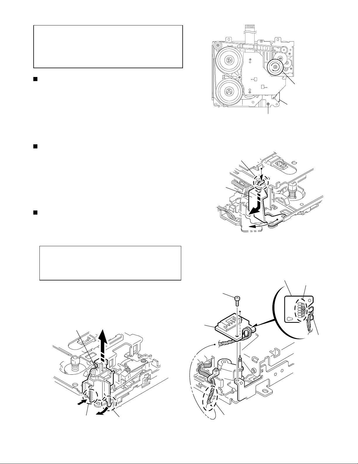
Disassembly method
<Main body>
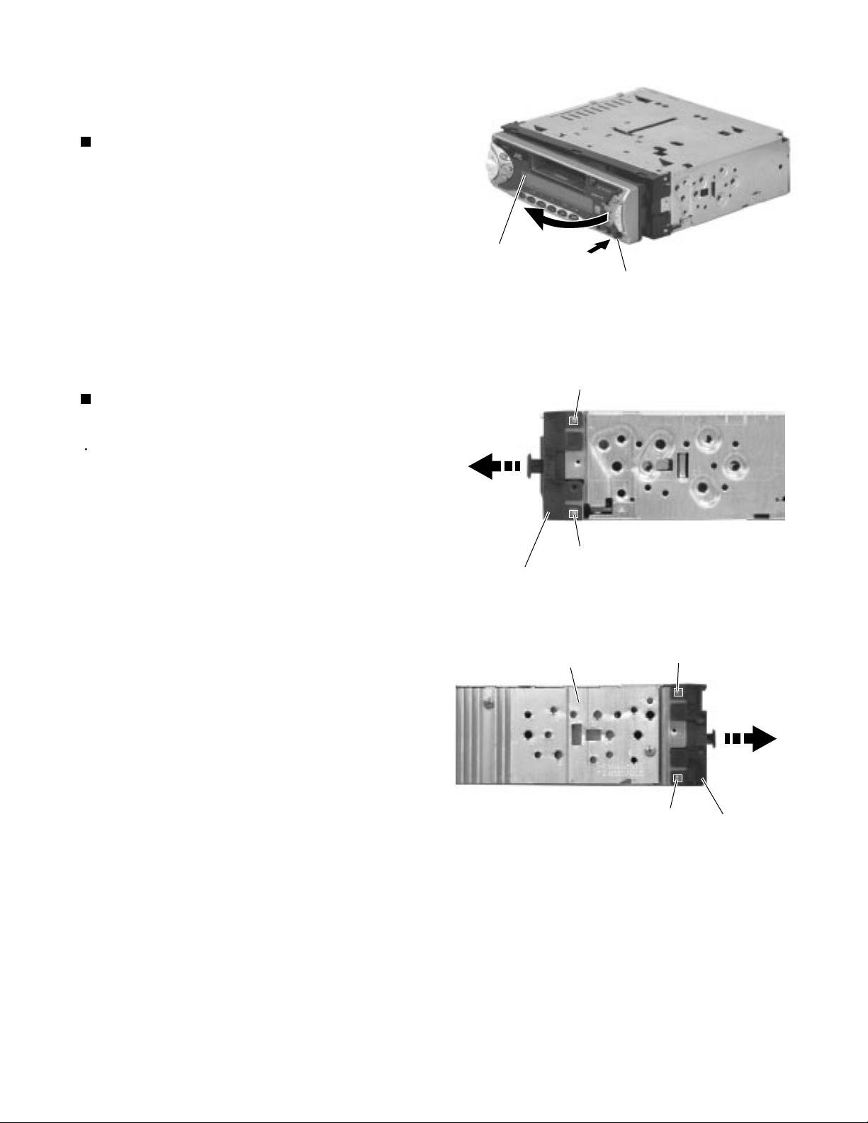
Removing the front panel assembly
(See Fig.1)
1.
Press the eject button in the lower right part of the
front panel. Remove the front panel assembly from
the body.
Removing the front chassis assembly
(See Fig.2 and 3)
KS-FX732R
Front panel assembly
Eject button
Fig.1
Tab a
Prior to performing the following procedure, remove
the front panel assembly.
1.
Release the four joint tabs a on both sides of the
front chassis assembly and remove the front chassis
assembly toward the front.
Tab a
Front chassis assembly
Heat sink
Fig.2
Tab a
Tab a
Front chassis
assembly
Fig.3
1-3
Page 4
KS-FX732R
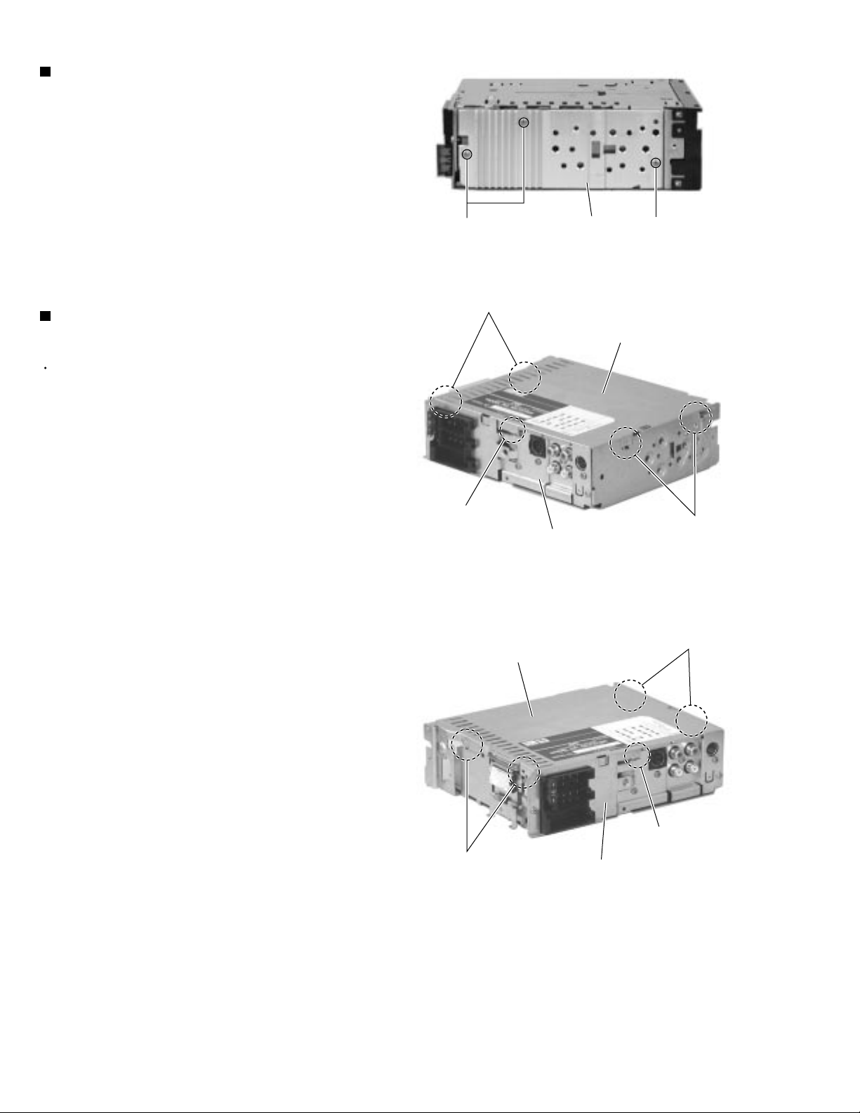
Removing the heat sink (See Fig.4)
1.
Remove the three screws A on the left side of the
body.
Removing the bottom cover
(See Fig.5 and 6)
Prior to performing the following procedure, remove
the front panel assembly, the front chassis assembly
and the heat sink.
1.
Turn over the body and unjoint the five joints b with
the bottom cover and the body using a screwdriver.
Joint b
A
Joints b
Heat sink
Fig.4
Rear panel
Fig.5
A
Bottom cover
Joints b
Joints b
Bottom cover
Joints b
Joint b
Rear panel
Fig.6
1-4
Page 5
KS-FX732R
Removing the main board
(See Fig.7 and 8)
Prior to performing the following procedure, remove
the front panel assembly, the front chassis assembly,
the heat sink and the bottom cover.
1.
Remove the screw B, the three screws C and the
two screws D attaching the rear bracket on the back
of the body. Remove the rear panel.
2.
Remove the two screws E attaching the main board
on the bottom of the body. Disconnect connector
CP401 on the main board in the direction of the
arrow.
D
E
Rear panel
Fig.7
C
Main board
B
C
D
E
Removing the cassette mechanism section
(See Fig.9)
Prior to performing the following procedure, remove
the front panel assembly, the front chassis assembly,
the heat sink, the bottom cover and the main board.
1.
Remove the four screws F attaching the cassette
mechanism section on the back of the top chassis.
Fig.8
Cassette mechanism section
F
F
Fig.9
CP401
F
F
Top chassis
1-5
Page 6
KS-FX732R
Removing the control switch board
(See Fig.10 to 12)
Prior to performing the following procedure, remove
the front panel assembly.
1.
Remove the four screws G attaching the rear cover
on the back of the front panel assembly.
2.
Unjoint the eleven joints c with the front panel and
the rear cover.
3.
Remove the control switch board on the back of the
front panel.
G
G
Front panel
Rear cover
Joints c
G
G
Fig.10
Joints c
Joints c
Rear cover
Front panel
Joints c
Fig.11
Control switch board
Fig.12
1-6
Page 7
KS-FX732R
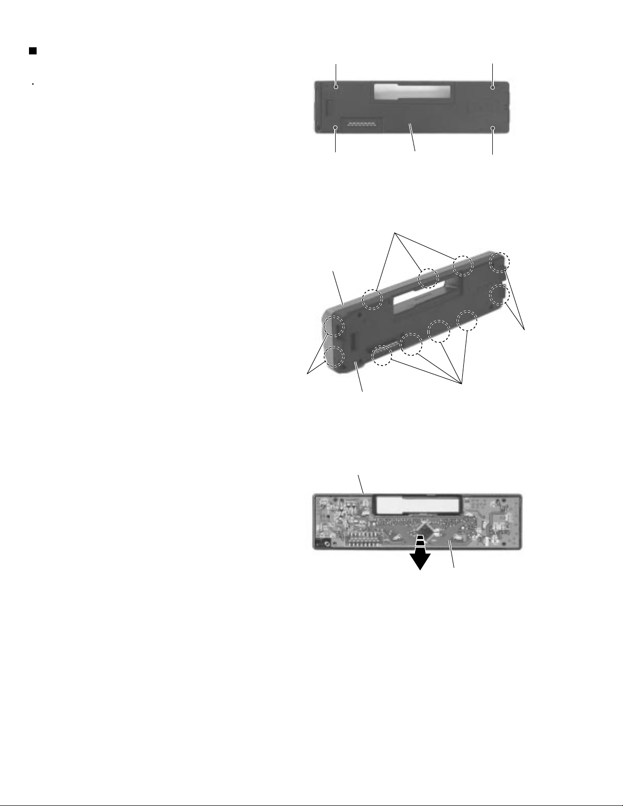
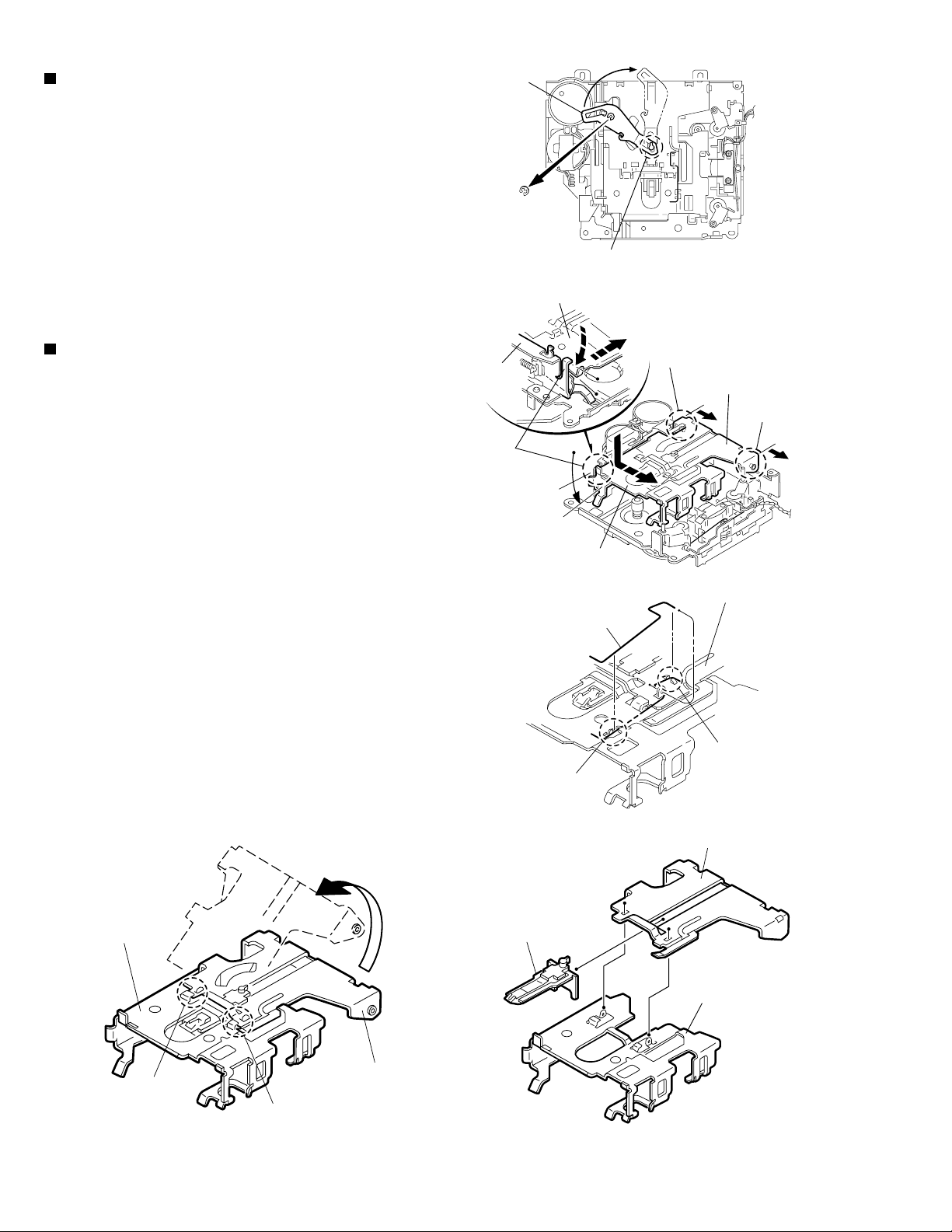
REFERENCE:
Prior to performing the following
procedures, turn the mode gear on the
bottom of the body until the respective part
comes to the EJECT position (Refer to
Fig.1).
Removing the reinforce bracket
(See Fig.1 and 2)
1.
Remove the screw A attaching the reinforce bracket
on the bottom of the body.
2.
To release joint a, turn and detach the reinforce
bracket from the side bracket assembly as shown in
Fig.2
Removing the cassette guide (See Fig.3)
1.
Turn the mode gear to set to RVS play or
subsequent mode.
2.
Remove the cassette guide from the main chassis
while releasing each two joint tabs b in the direction
of the arrow.
Mode gear
Reinforce bracket
A
Fig.1
Joint a
Reinforce bracket
Removing the head board (See Fig.4)
1.
Remove the screw B on the upper side. Unsolder
the wires on the under side of the head board, if
necessary.
REFERENCE:
Cassette guide
When reassembling, twist the wires by
turning the head board twice remarked c
and pass through the notch d as shown
in Fig.4.
Head board
B
Fig.2
Head board
Soldering
notch d
Tab b
Tab b
c
Fig.4Fig.3
1-7
Page 8
KS-FX732R
Removing the load arm (See Fig.5)
1.
Remove the E-washer attaching the load arm.
2.
Move the load arm in the direction of the arrow and
release the joint e on the cassette catch.
Removing the cassette hanger assembly /
cassette holder (See Fig.6 to 9)
1.
Check the mode is set to EJECT. Push down the
front part of the cassette holder and move in the
direction of the arrow to release the joint f.
2.
Move the rear part of the cassette hanger assembly
in the direction of the arrow to release it from the two
joint bosses g.
Load arm
E-washer
Cassette holder assembly
Side bracket
Joints f
Joint e
Fig.5
Boss g
Cassette hanger
assembly
Boss g
3.
Release the holder stabilizer spring from the hooks h
and i, then pull out from the cassette hanger
assembly.
4.
Bring up the rear side of the cassette hanger
assembly to release the joint j and k.
5.
Pull out the cassette catch from the cassette hanger
assembly.
Cassette holder
assembly
Cassette holder assembly
Fig.6
Cassette hanger assembly
Cassette stabilizer spring
Hook i
Hook h
Fig.7
Cassette hanger assembly
Cassette catch
Cassette holder assembly
1-8
Hook j
Fig.8
Cassette hanger assembly
Hook k
Fig.9
Page 9
KS-FX732R
Removing the side bracket assembly
(See Fig.10 to 12)
1.
Remove the screw C attaching the side bracket
assembly.
2.
Detach the front side of the side bracket assembly
upward and pull out forward to release the joint l and
m in the rear.
CAUTION:
CAUTION:
When reassembling, make sure that the
boss n of the main chassis is set in the
notch of the load rack under the side
bracket assembly. Do not reattach the
load rack on the boss n.
After reattaching the side bracket
assembly, confirm operation.
Side bracket assembly
Joint l
Joint m
C
Side bracket assembly
Fig.10
Side bracket assembly
Joint l
Joint m
Load rack
Load rack
Boss n
Boss n
Fig.11
Fig.12
1-9
Page 10

KS-FX732R
Removing the pinch arm (F) assembly
(See Fig.13 and 14)
1.
Remove the polywasher and pull out the pinch arm
(F) assembly.
2.
Remove the compulsion spring.
Removing the pinch arm (R) assembly
(See Fig.13 and 15)
1.
Remove the polywasher and pull out the pinch arm
(R) assembly.
Removing the slide chassis assembly
(See Fig.16 and 17)
Polywasher
Pinch arm
(R) assembly
Polywasher
Compulsion spring
Fig.13
Pinch arm
(F) assembly
Pinch arm (F) assembly
Polywasher
REFERENCE:
It is not necessary to remove the head
and the tape guide.
1.
Move the slide chassis assembly in the direction of
the arrow to release the two joints o and remove
from the main chassis.
2.
Remove the rack link.
CAUTION:
When reassembling, first reattach the rack
link, and next fit the boss p and hook q of
the slide chassis assembly to the hole of the
main chassis, and engage the two joints o.
Rack link
Fig.14
Boss p
Pinch arm
(R) assembly
Fig.15
Head
Hook q
Polywasher
Tape guide
Joint o
Slide chassis assembly
1-10
Fig.16
Joint o
Fig.17
Page 11

KS-FX732R
Removing the head / tape guide
(See Fig.18 and 19)
REFERENCE:
1.
Remove the band attaching the wire to the head.
2.
Remove the two screws D, the head and the head
support spring.
3.
Remove the pinch arm spring from the tape guide.
4.
Remove the tape guide and the pinch spring arm.
CAUTION:
CAUTION:
It is not necessary to remove the slide
chassis assembly.
When reattaching the pinch arm spring, set
both end of it to the pinch spring arm (
remarked r).
When reattaching the head, set the wires
into the groove of the tape guide (Fig.18).
D
Slide chassis assembly
Head
Tape guide
Fig.18
D
Pinch arm spring
Head
Head support spring
Tape guide
Removing the flywheel assembly (F) & (R)
(See Fig.20 and 21)
REFERENCE:
1.
Remove the belt at the bottom.
2.
Remove the two polywashers on the upper side.
3.
Pull out each flywheel assembly downward.
Flywheel assembly (F)
It is not necessary to remove the slide
chassis assembly.
Belt
r
Pinch spring arm
r
Slid chassis assembly
Fig.19
Polywasher
Polywasher
Flywheel assembly (R)
Fig.20
Flywheel assembly (F)
Fig.21
Flywheel assembly (R)
1-11
Page 12

KS-FX732R
Disassembling the flywheel assembly (F)
(See Fig.22 and 23)
1.
Push and turn counterclockwise the spring holder (F)
to release the three joints s on the bottom of the
flywheel.
2.
The spring holder (F), the TU spring and the friction
gear play come off.
3.
Remove the polywasher and felt.
Flywheel assembly (F)
Joints s
Flywheel assembly (R)
Joints t
Disassembling the flywheel assembly (R)
(See Fig.22 and 24)
1.
Push and turn clockwise the spring holder (R) to
release the three joints t on the bottom of the
flywheel.
2.
The spring holder (R), the FF spring and the friction
gear FF come off.
3.
Remove the polywasher and the felt.
Removing the reel board
(See Fig.25 and 26)
1.
Remove the two screws E attaching the reel board.
2.
Move the reel board in the direction of the arrow to
release the joint u.
3.
Unsolder the wires if necessary.
CAUTION:
When reattaching, confirm operation of
the MODE switch and the ST-BY switch.
The mode position between EJECT and
ST-BY is optimum for reattaching.
Joint s
Fig.22
Polywasher
Polywasher
Spring holder (R)
Spring holder (F)
TU spring
Friction gear FF
Friction gear play
Felt
Flywheel assembly (F)
FF spring
Felt
Flywheel assembly (R)
Fig.23 Fig.24
Joint t
1-12
Connect the card wire extending from
the reel board to the FFC pad before
reattaching the reel board.
FFC pad
E
Reel board
E
Fig.25
Joint u
FFC pad
CT-1 switch
MODE switch
Soldering
ST-BY switch
Fig.26
Page 13

KS-FX732R
Removing the gear base arm / gear base
link assembly (See Fig.27 to 29)
1.
Move the gear base arm in the direction of the arrow.
2.
Insert a slotted screwdriver to the gear base spring
under the gear base arm, and release the gear base
arm upward from the boss on the gear base
assembly.
3.
Remove the gear base arm from the main chassis
while releasing the two joints v.
4.
Move the gear base link assemby in the direction of
the arrow to release the two joints w.
REFERENCE:
When reattaching the gear base arm,
make sure that the boss on the gear
base assembly is inside the gear base
spring.
Removing the FFC pad
(See Fig.27 and 29)
Gear base
link assembly
Gear base spring
Joint w
Gear base arm
Joints v
Hook x
FFC pad
Hook x
Joint w
Fig.27
Gear base arm
Screwdriver
1.
Push each joint hook x of the FFC pad and remove
toward the bottom.
Gear base link assembly
Fig.28
Gear base arm
Fig.29
FFC pad
1-13
Page 14

KS-FX732R
Removing the mode gear
(See Fig.30 and 33)
1.
Remove the polywasher on the bottom and pull out
the mode gear.
Removing the mode switch actuator
(See Fig.30, 31 and 33)
1.
Pull out the mode switch actuator at the bottom.
REFERENCE:
When reattaching the mode switch
actuator to the main chassis, make sure to
set on the shaft and insert y into the slot z.
Removing the direction link / direction
plate (See Fig.31 to 33)
1.
Remove the polywasher attaching the direction link.
2.
Bring up the direction link to release the three joints
a’, b’ and c’ at a time.
3.
Move the direction plate in the direction of the arrow
to release the two joints d’.
REFERENCE:
When reattaching the direction plate,
engage the two joints d’ and move in the
direction of the arrow (See Fig.32).
Mode switch actuator
Direction plate
Direction link
Fig.30
Direction plate
Joints d'
Joint c'
Direction link
Slot z
Joint b'
Polywasher
Fig.31
Direction plate Mode rack assembly
Joint k'
Mode gear
Polywasher
Mode rack assembly
Joint a'
Joint k'
Joint l'
REFERENCE:
When reattaching the direction link,
move the direction plate in the direction
of the arrow and engage the three joint
a’, b’ and c’ at a time (See Fig.33).
Removing the mode rack assembly
(See Fig.31 and 32)
1.
Move the mode rack assembly in the direction of the
arrow to release the two joints k’ and the joint l’.
REFERENCE:
When reattaching, set the two k’ on the
bottom of the mode rack assembly into the
slots of the main chassis and move in the
direction of the arrow (See Fig.32).
Joints d'
Fig.32
Direction link
Mode switch actuator
Polywasher
y
Mode gear
Direction plate
Mode rack assembly
Fig.33
1-14
Page 15

KS-FX732R
Removing the gear base assembly / take
up gear / reflector gear (See Fig.34 to 36)
1.
Push in the pin e’ of the gear base assembly on the
upper side of the body and move the reflector gear
toward the bottom, then pull out.
2.
Remove the polywasher on the bottom and pull out
the take up gear.
3.
Move the gear base assembly in the direction of the
arrow to release it from the two slots f’ of the main
chassis.
REFERENCE:
The parts are damaged when removed.
Please replace with new ones.
Gear base assembly
Pin e'
Polywasher
Slot f'
Slot f'
Fig.34
Take up gear
Removing the reel driver / reel spindle
(See Fig.36)
1.
Draw out the reel driver from the shaft on the main
chassis and remove the reel driver spring and the
reel spindle respectively.
CAUTION:
The reel driver is damaged when
removed. Please replace with a new
one.
Reflector gear
Reel driver
Reel driver spring
Reel spindle
Main chassis
Fig.35
Reel driver
Reel driver spring
Reel spindle
Gear base assembly
Slots f’
Take up gear
Reflector gear
Polywasher
Fig.36
1-15
Page 16

KS-FX732R
Removing the side bracket assembly
(See Fig.37 to 41)
1.
Remove the eject cam plate spring.
2.
Push the joint g‘ through the slot to remove the load
rack downward.
3.
Move the eject cam limiter in the direction of the
arrow to release it from the boss h’ of the side
bracket assembly and from the two joints i’.
4.
Move the eject cam plate in the direction of the arrow
to release the joint j’.
Joint g'
CAUTION:
Joint i'
When reassembling, confirm operation of
each part before reattaching the eject cam
plate spring.
Side bracket assembly
Boss h'
Eject cam limiter
Side bracket assembly
Joint i'
Joint g'
Eject cam plate spring
Joint i'
Load rack
Fig.37
Boss h'
Eject cam limiter
Eject cam plate
Fig.39
Joint i'
1-16
Fig.38
Side bracket assembly
Boss h'
Eject cam plate
Fig.40
Load rack
Joint j'
Side bracket assembly
Eject cam plate
Joint j'
Fig.41
Page 17

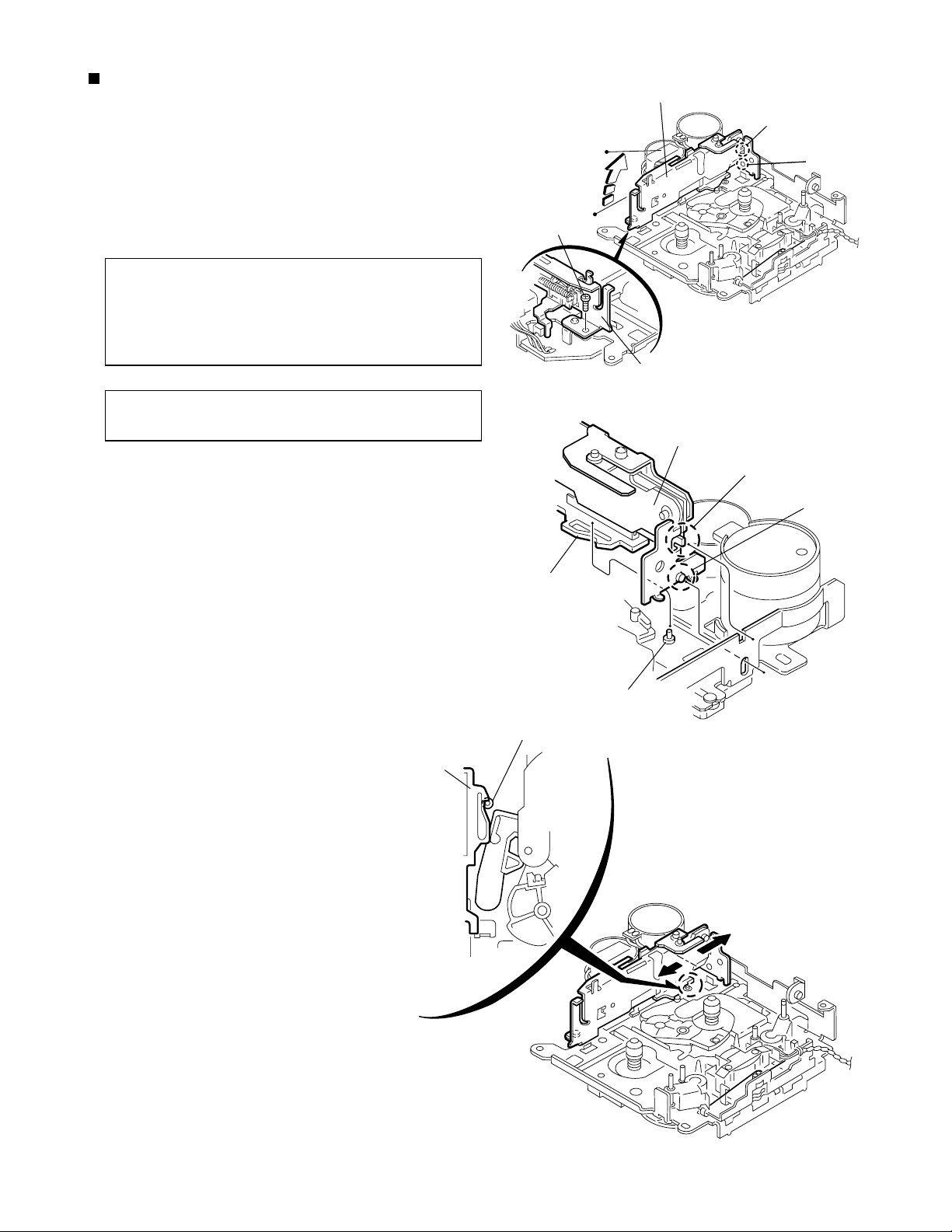
KS-FX732R
Removing the main motor assembly /
sub motor assembly (See Fig.42 to 44)
1.
Remove the belt at the bottom.
2.
Remove the polywasher and pull out the mode gear.
3.
Pull out the reduction gear (B).
4.
Remove the polywasher and pull out the reduction
gear (A).
5.
Remove the two screws F attaching the main motor
assembly.
6.
Remove the two screws G attaching the sub motor
assembly.
7.
Unsolder the wires on the reel board if necessary.
CAUTION:
When reassembling, adjust the length of the
wires extending from the sub motor
asswmbly by attaching them to the side of
the sub motor assembly with the wires
extending from the main motor assembly
using a spacer.
Belt
Reduction gear (B)
Reduction gear (B)
G
Polywasher
Fig.42
F
G
Mode gear
Polywasher
Reduction gear (A)
F
Main motor
assembly
Reduction
gear (A)
Polywasher
Sub motor
assembly
Spacer
Main motor assembly
Sub motor assembly
Main motor assembly
Sub motor assembly
Fig.43
Spacer
Fig.44
1-17
Page 18

KS-FX732R
Adjustment method
Test instruments reqired for adjustment
1. Digital osclloscope(100MHz)
2. Frequency Counter meter
3. Electric voltmeter
4. Wow & flutter meter
5. T est Tapes
MC-109C
VT724.......................
VT739............For playback frequency measurement
VT712....For wow flutter & tape speed measurement
VT703..................... For head azimuth measurement
6. T orque gauge ....................Cassette type for CTG-N
...................
for TAPA CURL confirmation
(without Padd type)
for DOLBY level measurement
(mechanism adjustment)
Standard volume position
Balance and Bass,Treble volume. Fader
:Center(Indication"0")
Loudness,Dolby NR,Sound,Cruise:Off
Volume position is about 2V at speaker output with
following conditions.Playback the test tape VT721.
FM: 87.5 MHz to 108.0 MHz
AM: (MW)522 kHz to 1
Measuring conditions(Amplifier section)
Power supply voltage.............. DC14.4V (11V to 16V allowance))
Load impedance ........... 4 (4 to 8 allowance)
Line out............................................................ 20k (250 nWb/m)
620 kHz
(LW) 144 kHz to 279 kHz
1-18
Page 19

Arrangement of adjusting & test points
Cassette mechanism
(Surface)
Motor assembly
KS-FX732R
Tape speed adjust
Head section view
Azimuth screw A
(Forward)
Playback head
Azimuth screw B
(Reverse)
Azimuth screw B
(Reverse)
Azimuth screw A
(Forward)
Playback Head
1-19
Page 20

KS-FX732R
Information for using a car audio service jig
1. We're advancing efforts to make our extension cords common for all car audio products.
Please use this type of extension cord as follows.
2. As a U-shape type top cover is employed, this type of extension cord is needed to check operation of the
mechanism assembly after disassembly.
3. Extension cord : EXTKSRT002-18P ( 18 pin extension cord ) For connection between mechanism assembly
and main board assembly .
Check for mechanism driving section such as motor ,etc..
Disassembly method
1. Remove the bottom cover.
2. Remove the front panel assembly.
3. Remove the top cover .
4. Install the front panel.
5. Confirm that current is being carried by connecting
an extension cord jig.
Note
Available to connect to the CP701 connector when installing the front panel.
Cassette mechanism
to Cassette mechanism
EXTKSRT002-18P
Extension cord
EXTKSRT002-18P
to Main board
Main board
Front panel assembly
1-20
Page 21

Mechanism adjustment section
Item Adjusting & Confirmation Methods Adjust Std. Value
1. Tape running
adjustment
2. Azimuth
adjustment
confirmation
a) At Forward playmode, using mirror tape, make adjustment
with Azimuth screw A and Azimuth screw B, without curl of 4
parts of head tape guide.
b) At Reverse play mode, using mirror tape, make adjustment
with Azimuth screw A and Azimuth screw B, without tape
curl of 4 parts of head guide.
c) At Forward / Reverse play mode, make confirmation of no
tape curl of 4 parts of head tape guide.
a) At forward play mode, make adjustment of peak of Lch / Rch
output with Azimuth screw A.
* For Oscilloscope litharge corrugation, set 45 as standard.
b) At Reverse play mode, make adjustment of peak of Lch / Rch
output with Azimuth screw B.
* For Oscilloscope litharge corrugation, set 45 as standard.
c) With AC volt meter confirm the difference of output for 4ch
between Lch / Rch at forward play mode and Lch / Rch
Reverse play mode being within 3.0dB.
d) After operation, make confirmation of Lch / Rch azimuth
output being within 1.0dB from adjustment value.
KS-FX732R
Azimuth
screw A
Azimuth
screw B
2.T ape Speed and
Wow & Flutter
HEAD
Tape guide
OK
HEAD TAPE
1.Check to see if the reading of the frequency counter & W ow
flutter meter is within 2940-3090 Hz( FWD/REV ), and less
than 0.35% ( JIS RMS ).
2.In case of out of specification, adjust the motor with a builtin volume resistor .
Tape curl NG
0
Phase
Built-in
volume resistor
45
T ape Speed
2940-3090Hz
Wow&Flutter
Less than
0.35%
(JIS RMS)
3.Playback
Frequency
response
1.Play the test tape ( VT724 : 1kHz ) back and set the volume
position at 2V .
2.Play the test tape ( VT739 )back and confirm 0 3dB at1kHz/
10kHz and -4+2dB at 1kHz/63Hz.
3.When 10kHz is out of specification, it will be necessary to
read adjust the azimuth.
Speaker out
1kHz/10kHz
: 0dB 3dB,
63Hz/1kHz
: -4dB+2dB,
1-21
Page 22

KS-FX732R
Description of major ICs
HA13164A(IC901):Regulator
1.Terminal layout
EXT
ANTOUT
ACC-IN
5.6V
SW5V
ACC-HOLD
ANTCTR
MEMORY
123456789101112131415
2.Block diagram
MEMDET9VPWR-CNT8VILL-10V
ILL-ADJ
GND
3.Pin function
11
12
10
8
2
1
7
Surge Protector
BIAS TSD
15
3
TAB
note1) TAB (header of IC)
13
connected to GND
9
6
4
5
14
UNIT R:
C:F
1-22
Pin No. Symbol Function
1
2
EXT
ANTOUT
Output voltage is VCC-1 V when M or H level applied to CTRL pin.
Output voltage is VCC-1 V when M or H level to CTRL pin and H level
to ANT-CTRL.
3
4
5
6
7
8
9
10
11
12
13
14
15
ACC-IN
5.6V
SW5V
ACC-HOLD
ANTCTR
MEMORY
MEMDET
9V
PWR-CNT
8V
ILL-10V
ILL-ADJ
GND
Connected to ACC.
Regular 5.6V.
Output voltage is 5V when M or H level applied to CTRL pin.
Output for ACC detector.
L:ANT output OFF , H:ANT output ON
Connected to VCC.
Low battery detect.
Output voltage is 9V when M or H level applied to CTRL pin.
L:BIAS OFF, M:BIAS ON, H:CD ON
Output voltage is 8V when H level applied to CTRL pin.
Adjustment pin for ILM output voltage.
Output voltage is 10V when M or H level applied to CTRL pin.
Connected to GND.
Page 23

CXA2559Q(IC401):Playback equalizer amplifier with music sensor
30
29
28
27
26
1.Pin layout
10
3.Pin function
2.Blockdiagram
31
1
30
21
32
33
34
35
36
37
38
39
40
45k
7k/12k
300k
300k
7k/12k
1
30k
30k
+
F2
F1
+
-
2
100k
X1
X1
100k
3
4
25
T2
BIAS
MUTE
TAPE EQ
FWD/RVS
LPF
T1
5
6
Vcc
F3
KS-FX732R
24
23
22
21
24dB
-
+
MS MODE
-
24dB
8
DET
9
+
-
+
7
MS ON/
OFF
10
20
19
18
17
16
15
14
13
12
11
Pin No.
1
2
3
4
5
6
7
8
9
10
11
12
13
14
15
16
17
18
19
20
21
22
23
24
25
26
27
28
29
30
31
32
33
34
35
36
37
38
39
40
Symbol
PBTC1
PBOUT1
OUTREF1
TAPEIN1
Vcc
NC
OUT1
TCH1
NC
MSLPF
G2FB
GI1FB
MSTC
MSOUT
NC
NRSW
MUTE
METAL
DIRECTION
FF/REW
MSSW
NC
TCH2
OUT2
DIREF
GND
TAPEIN2
OUTREF2
PBOUT2
PBTC2
PBFB2
PNRIN2
PBGND
PBFIN2
VCT
PBREF
PBFIN1
PBGND
PBRIN1
PBFB1
I/O
Function
-
Terminal of capacity of reproduction equalizer reproduction
O
Equalizer output terminal
O
Output standard terminal
I
Tape input terminal
-
Power supply terminal
-
Non connection
O
Line-out output terminal
Time constant for the HLS
-
Non connection
-
Detection LPF terminal between tunes
-
Detection level set terminal between tunes
-
Detection level set terminal between tunes
-
Time constant connection terminal for the detection between tunes
O
Detection output terminal between tunes
-
Non connection
Dolby NR control
I
Mute function control terminal
I
Reproduction equalizer control terminal
I
Head change control terminal
I
Detection mode control terminal between tunes
I
Detection function control terminal between tunes
-
Non connection
Time constant for the HLS
O
Line-out output terminal
-
Resistance connection terminal for standard current setting
-
Earth terminal
I
Tape input terminal
O
Output standard terminal
O
Reproduction equalizer output terminal
-
Terminal of capacity of reproduction equalizer
I
Reproduction equalizer return terminal
I
Reproduction equalizer input terminal
-
Reproduction equalizer system earth terminal
I
Reproduction equalizer input terminal
O
Middle point terminal
O
Reproduction equalizer standard terminal
I
Reproduction equalizer input terminal
-
Reproduction equalizer system earth terminal
I
Reproduction equalizer input terminal
I
Reproduction equalizer return terminal
1-23
Page 24

KS-FX732R
UPD178018AGC-585(IC701) : Main system control CPU
1. Pin layout
2. Pin function
Pin No.
1
2
3
4
5
6
7
8
9
10
11
12
13
14
15
16
17
18
19
20
21
22
23
24
25
26
27
28
29
30
31
32
33
34
35
36
37
38
39
40
80 ~ 61
1
~
20
21 ~ 40
60
~
41
Port Name I/O Descriptions
KEY 0
KEY 1
KEY 2
LEVEL
SM
SQ
LCDCE
LCDDA
LCDSCK
BUSI/O
OPEN
BUSSI
BUSSO
BUSSCK
NC
NC
NC
NC
INLOCK
NC
GNDPORT
VDDPORT
NC
AFCK
MONO
FM/AM
SEEK/STOP
NC
IFC
VDDPLL
FMOSC
NC
GNDPLL
AMEO
FMEO
IC
SD/ST
STAGE0
NC
MOTOR
I
I
I
I
I
I
O
O
O
I
I
I
O
I/O
-
-
-
-
-
-
-
O
O
O
O
O
I
I
-
I
-
O
O
-
I
I
O
Key input 0
Key input 1
Key input 2
Level meter input
S.meter level input
S.Quality level input
CE output to LCD driver
Data output to LCD driver
Clock output to LCD driver
I/O selector output for J-BUS, H : OUT, L: INPUT
Door open detect input
J-BUS Data input
J-BUS Data output
J-BUS Clock in/output
Non connect
Non connect
Non connect
Non connect
Non connect
Non connect
Port GND
Port Vdd
Non connect
AF check output, L: AF check
Monaural on /off selecting output, H:mono on
FM/AM switching output L : FM H : AM
Auto seek /stop selecting output, H: Seek, L:Stop
Pulse signal input port for Cruise control
FM/AM midle frequency counter input
PLL Vdd
FM/AM limited generator frequency input
None connect
PLL GND
AM error out output
FM error out output
GND
Station detector, Stereo signal input, H:Find Station, L:Stereo
Pull up
Non connect
Main motor output
1-24
Page 25

Pin No.
41
42
43
44
45
46
47
48
49
50
51
52
53
54
55
56
57
58
59
60
61
62
63
64
65
66
67
68
69
70
71
72
73
74
75
76
77
78
79
80
Port Name I/O Descriptions
FF/REW
F/R
DOLBY
MSIN
I2CCLK
I2CDAO
I2CDAI
REEL
SUBMO1
SUBMO2
MODE
TAPEIN
STANDBY
NC
NC
NC
NC
NC
NC
MUTE
PCNT
TELMUTE
NC
NC
NC
NC
ACCDET
POWER
RDSSCK
RDSDA
REMOCON
DETACH
J-BUSINT
REGCPU
GND
X2
X1
REGOSC
VDD
RESET
I
O
O
I
O
O
I
O
I
O
O
O
I
-
-
-
-
-
O
O
I
-
-
-
-
I
O
I
I
I
I
I
-
-
-
I
-
-
-
Output for input signal lev el s witching f or MS L : FF,REW H : PLAY
FWD,REV running direction s witch signal input
Dolby on "H" output
MS input
I2C information clock output
I2C information data output
I2C information clock input
Switch for detecting tape end position
Sub motor clock direction input
Sub motor clock opposite detection drive output
Mechanism mode position detection input
Cassette in detection input H : cassette in L : cassette out
Standby position detection input H : eject side L : operation side
Non connect
Non connect
Non connect
Non connect
Non connect
Non connect
Mute output , L : mute on
Power ON /OFF switching output , H : power on
Telephone mute signal detection input
Non connect
Non connect
Non connect
Non connect
Power sa v e 1 Working togethe ACC Power save : L
Power sa v e 2, Working together Back up by H input, stop mode
Clock input for RDS
RDS data input
Remocom input
Detach signal input H : Power save
Cut-in input for J-BUS signal
Regulator for CPU power supply, Connect the GND with0.1 F.
Ground
Connecting the crystal oscillator for system clock
Connecting the crystal oscillator for system clock
Regulator for oscillator circuit.Connect the GND with 0.1 F.
Vdd
Pull up
KS-FX732R
UPD178018AGC-585(2/2)
1-25
Page 26

KS-FX732R
LA4743K(IC301):Power AMP
1.Block diagram
6 20
11
1
12
4
10
Stand by
Switch
Ripple
Filter
-
+
Protective
circuit
-
+
Mute
circuit
+
9
-
7
8
+
5
3
2
22
1-26
15
25
13
14
16
Muting &
ON Time Control
Circuit
-
+
Protective
circuit
-
+
+
17
-
19
18
+
21
-
23
24
Page 27

2.Terminal layout
TAB
GND
KS-FX732R
RROUT-
STANBAY
RROUT+
VCC
FRONT-
GND
FRONT+
RIPPLE
FRIN
RRIN
SGND
RLIN
FLIN
ONTIME
FLOUT+
GND
FLOUT-
VCC
RLOUT+
MUTE
RLOUT-
GND
NC
3.Pin function
1
2
3
4
5
6
7
8
9
10
11
12
13
14
15
16
17
18
19
20
21
22
23
24
25
SymbolPin No. Function
TAB
GND
RROUTSTANBAY
RROUT+
VCC
FRONTGND
FRONT+
RIPPLE
FRIN
RRIN
SGND
RLIN
FLIN
ONTIME
FLOUT+
GND
FLOUTVCC
RLOUT+
MUTE
RLOUTGND
NC
Header of IC
Power GND
Outpur(-) for front Rch
Stand by input
Output (+) for front Rch
Power input
Output (-) for rear Rch
Power GND
Output (+) for rear Rch
Ripple filter
Rear Rch input
Front Rch input
Signal GND
Front Lch input
Rear Lch input
Power on time control
Output (+) for rear Lch
Power GND
Output (-) for rear Lch
Power input
Output (+) for front
Muting control input
Output (-) for front
Power GND
No connection
LA4743K
1-27
Page 28

KS-FX732R
LC75823W (IC651) : LCD driver
1. Pin Layout & Symbol
DI
CLOCKCEOSC
64 63 62 61 60 59 58 57 56 55 54 53 52 51 50 49
1
S1
2
S2
3
S3
4
S4
5
S5
6
S6
7
S7
8
S8
9
S9
10
S10
11
S11
12
S12
13
S13
14
S14
15
S15
16
S16
17 18 19 20 21 22 23 24 25 26 27 28 29 30 31 32
Vss
VDD2
VDD1
INH
VDD
COM3
COM2
COM1
S52
S51
S50
S49
48
47
46
45
44
43
42
41
40
39
38
37
36
35
34
33
S48
S47
S46
S45
S44
S43
S42
S41
S40
S39
S38
S37
S36
S35
S34
S33
2. Pin Function
Pin No.
3 to 52
53 to 55
56
57
60
61
63
S17
S18
Symbol
S3 to S52
COM1 to COM3
VDD
INH
Vss
OSC
CLOCK
S19
S20
S21
S22
S23
S24
S25
S26
S27
S28
S29
S30
S31
S32
I/O
O
Segment output pins used to display data transferred
Function
by serial data input.
O
Common driver output pins. The frame frequency is given
by : t0=(fosc/384)Hz.
--
Power supply connection. Provide a voltage of between
4.5 and 6.0V.
I
Display turning off input pin.
INT="L" (Vss) ----- off (S1 to S52, COM1 to COM3="L"
INT="H" (VDD)----- on
Serial data can be transferred in display off mode.
--
Power supply connection. Connect to GND.
I/O
Oscillator connection.
An oscillator circuit is formed by connecting an external
resistor and capacitor at this pin.
I
Serial data
interface connection to the controller. CL : Sync clock
1-28
Page 29

SAA6579T-X(IC71):RDS
1.Pin layout
1
DATA
2
Vref
3
MUX
4
Vdd
5
GND
6
CIN
7
SOUT
8
2.Block diagram
KS-FX732R
CLK
16
15
OSCO
14
OSCI
13
Vdd
12
GND
11
TEST
10
MODE
9
121413
3.Pin function
4
8
7
CLOCKED
COMPARATOR
5
3
REFERENCE
VOLT AGE
Pin No.
1
2
3
4
ANTIALIASING
FILTER
6 11
Symbol
VP1
57 kHz
BAND PASS
(8th ORDER)
COSTAS LOOP
VARIABLE AND
FIXED DIVIDER
CLOCK
REGERATION
AND SYNC
RECONSTRUCTION
FILTER
TEST LOGIC AND OUTPUT
SELECTOR SWITCH
Description
OSCILLATOR
AND
DIVIDER
BIPHASE
SYMBOL
DECODER
910
No connect
DATA
Vref
MUX
RDS data output
Reference voltage output (0.5V
Multiplex signal input
DDA
QUALITY BIT
GENERATOR
DIFFERENTIAL
DECODER
)
1
2
16
15
10
11
12
13
14
15
16
5
6
7
8
9
Vdd
GND
CIN
SOUT
MODE
TEST
GND
Vdd
OSCI
OSCO
+5V supply voltage for analog part
Ground for analog part (0V)
Sub carrier input to comparator
Sub carrier output of reconstruction filter
Oscillator mode / test control input
Test enable input
Ground for digital part (0V)
+5V supply voltage for digital part
Oscillator input
Oscillator output
No connect
CLK
RDS clock output
1-29
Page 30

KS-FX732R
TEA6320T-X (IC161) : E.volume
1.Pin layout
2.Block diagram
10 8 9 7 6
5
12
SDA
1
GND
2
OUTRL
OUTFL
MUTE
TL
B2L
B1L
IVL
ILL
QSL
IDL
ICL
IMD
IBL
IAL
3
4
5
6
7
8
9
10
11
12
13
14
15
16
3.Pin functions
Pin
Symbol
No.
SDA
1
SCL
32
VCC
31
OUTRR
30
OUTRF
29
TR
28
B2R
27
B1R
26
IVR
25
ILR
24
QSR
23
IDR
22
VREF
21
ICR
CD-CH
TAPE
TUNER
20
19
18
17
CAP
IBR
IAR
I/O
Serial data input/output.
I/O
MUTE
21
31
2
19
16
15
13
11
14
22
20
18
17
Functions Functions
POWER
SUPPLY
SOURCE
SELECTOR
23 25 24 26 27 28
VOLUME 1
+20 to -31 dB
LOUDNESS
LEFT
VOLUME 1
+20 to -31 dB
LOUDNESS
RIGHT
Pin
No.
17
Symbol
IAR
BASS
LEFT
+15 dB
LOGIC
BASS
RIGHT
+15 dB
I/O
I
Input A right source.
TREBLE
LEFT
+12 dB
TREBLE
RIGHT
+12 dB
FUNCTION
ZERO CROSS
DETECTOR
VOLUME 2
0 to 55 dB
BALANCE
FENDER REAR
VOLUME 2
0 to 55 dB
BALANCE
FENDER FRONT
HC BUS
REC
VOLUME 2
0 to -55dB
BALANCE
FENDER FRONT
VOLUME 2
0 to -55dB
BALANCE
FENDER REAR
3
4
32
1
29
30
2
3
4
5
6
7
8
9
10
11
12
13
14
15
16
GND
OUTRF
OUTFL
TL
B2L
B1L
IVL
ILL
QSL
IDL
MUTE
ICL
IMO
IBL
IAL
Ground.
output left rear.
O
output left front.
O
Treble control capacitor left channel or
I
input from an external equalizer.
Bass control capacitor left channel or
-
output to an external equalizer.
Bass control capacitor left channel.
Input volume 1. left control part.
I
Input loudness. left control part.
I
Output source selector. left channel.
O
Not used
Not used
Input C left source.
I
Not used
Input B left source.
I
Input A left source.
I
18
19
20
21
22
23
24
25
26
27
28
29
30
31
32
IBR
CAP
ICR
VREF
IDR
QSR
ILR
IVR
B1R
B2R
TR
OUTRF
OUTRR
Vcc
SCL
I
Input B right source.
-
Electronic filtering for supply.
I
Input C right source.
-
Reference voltage (0.5Vcc)
-
Not used
O
Output source selector right channel.
I
Input loudness right channel.
I
Input volume 1. right control part.
-
Bass control capacitor right channel
Bass control capacitor right channel or
O
output to an external equalizer.
Treble control capacitor right channel or
I
input from an external equalizer.
O
Output right front.
O
Output right rear.
-
Supply voltage.
I
Serial clock input.
1-30
Page 31

HD74HC126FP-X (IC751) : Buffer
KS-FX732R
1.Terminal layout
1
2
3
4
5
6
7
2.Block diagram
Input
14
13
12
11
10
9
8
Vcc Vcc
1A
2A
3A
4A
1C
2C
3C
See Function Table
4C
3.Pin function
Output
1Y
2Y
Output
2Y
Output
3Y
Output
4Y
Input Outout
C
A
L
X
H
L
H
H
Y
Z
H
L
1k
S1
CL
1k
Sample as Load Circuit 1
Sample as Load Circuit 1
Sample as Load Circuit 1
LB1641 (IC402) : DC motor driver
1. Pin layout
1 2 3 4 5 6 7 8 9
GNDOUT1 P1
VZ IN1 IN2
VCC1
VCC2 P2
10
OUT2
2. Pin function
Input Output
IN1 IN2 OUT1 OUT2
0 0 0 0
1 0 1 0
0 1 0 1
1 1 0 0
Mode
Brake
CLOCKWISE
COUNTER-CLOCKWISE
Brake
1-31
Page 32

KS-FX732R
VICTOR COMPANY OF JAPAN, LIMITED
MOBILE ELECTRONICS DIVISION
PERSONAL & MOBILE NETWORK BUSINESS UNIT. 10-1,1Chome,Ohwatari-machi,Maebashi-city,371-8543,Japan
(No.49695)
200202
 Loading...