

Page 1
49825200303
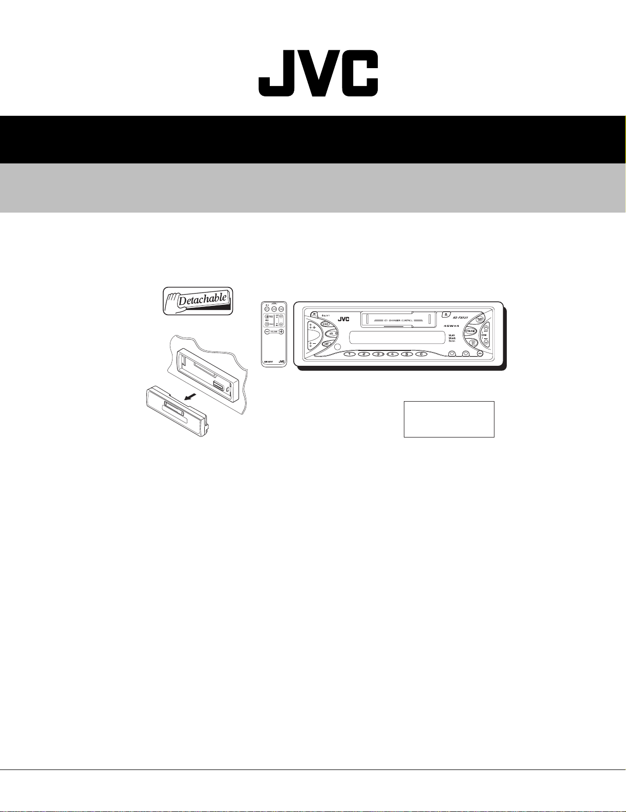
KS-FX621
SERVICE MANUAL
CASSETTE RECEIVER
KS-FX621
11
RPT
1097
12
8
MO
RND
S
C
M
MODE
Area Suffix
U ------ Other Areas
TABLE OF CONTENTS
1 Safety precaution . . . . . . . . . . . . . . . . . . . . . . . . . . . . . . . . . . . . . . . . . . . . . . . . . . . . . . . . . . . . . . . . . . . . . 1-2
2 Disassembly method . . . . . . . . . . . . . . . . . . . . . . . . . . . . . . . . . . . . . . . . . . . . . . . . . . . . . . . . . . . . . . . . . . 1-3
3 Adjustment. . . . . . . . . . . . . . . . . . . . . . . . . . . . . . . . . . . . . . . . . . . . . . . . . . . . . . . . . . . . . . . . . . . . . . . . . . 1-17
4 Description of major ICs. . . . . . . . . . . . . . . . . . . . . . . . . . . . . . . . . . . . . . . . . . . . . . . . . . . . . . . . . . . . . . . 1-21
COPYRIGHT © 2003 VICTOR COMPANY OF JAPAN, LTD.
No.49825
2003/03
Page 2

KS-FX621
SECTION 1
Safety precaution
CAUTION
Burrs formed during molding may be left over on some parts of the chassis. Therefore, pay attention to such burrs in
the case of preforming repair of this system.
1-2 (No.49825)
Page 3
SECTION 2
Disassembly method
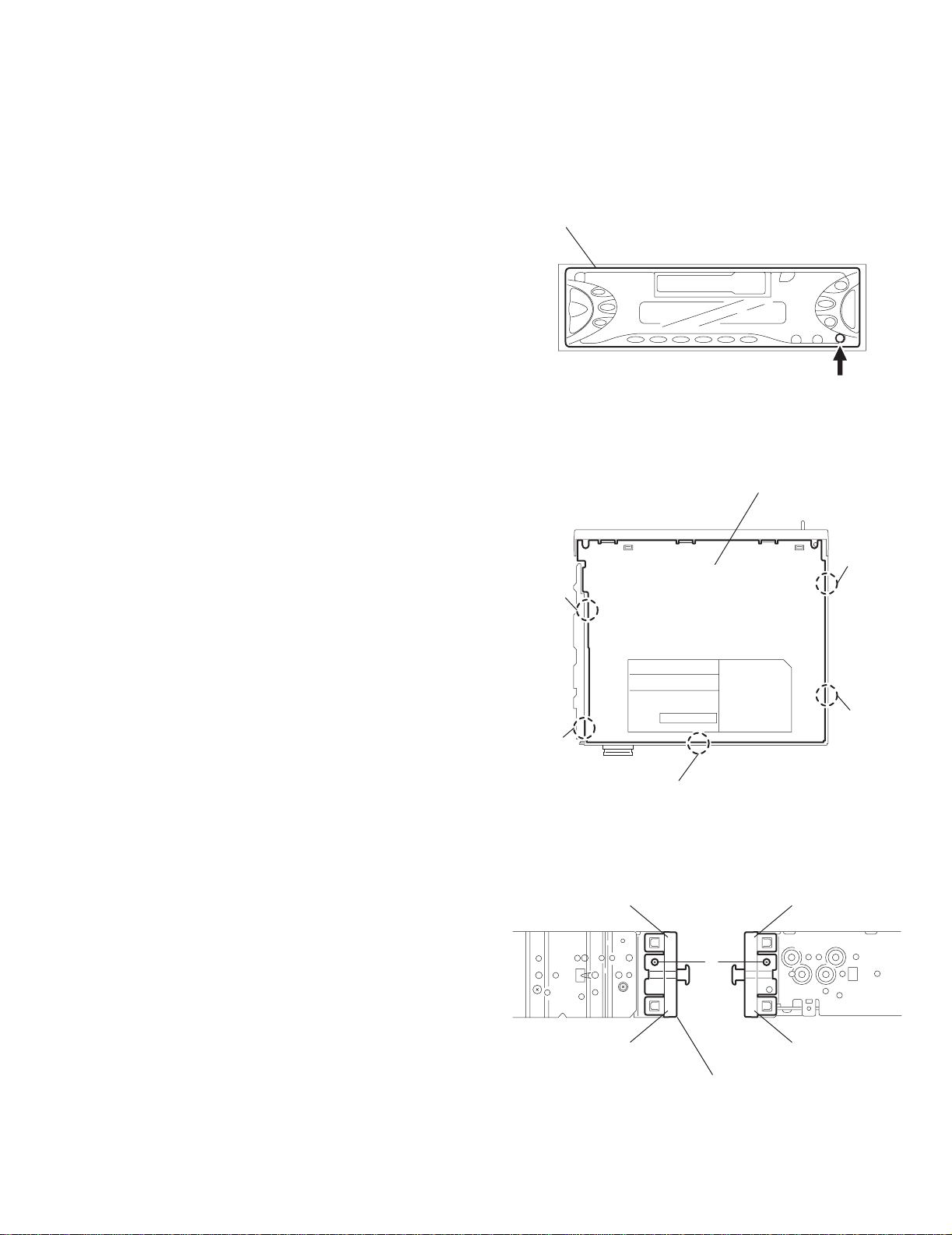
2.1 Main body
2.1.1 Removing the front panel assembly
(See Fig.1)
(1) Press the release button and remove the front panel as-
sembly.
2.1.2 Removing the bottom cover
(See Fig.2)
• Prior to performing the following procedure, remove the front
panel assembly.
(1) Turn the body upside down.
(2) Insert a screwdriver under the joints to release the two
joints a on the left si de, the two joints b on the right side and
the joint c on the back of the body, then remove the bottom
cover from the body.
CAUTION:
When releasing the joint c using a screwdriver, do not damage
the main board.
Front panel assembly
Joint a
Fig.1
Bottom cover
KS-FX621
Release button
Joint
b
2.1.3 Removing the front chassis
(See Fig.3)
• Prior to performing the following procedure, remove the front
panel assembly and bottom cover.
(1) Remove the screw A on each side of the body.
(2) Release the two joints d and the two joints e on the sides,
then remove the front chassis toward the front.
Joint a
Joint c
Fig.2
Joint d
Joint e
A
Joint d Joint e
Front chassis
Fig.3
Joint b
(No.49825)1-3
Page 4
KS-FX621
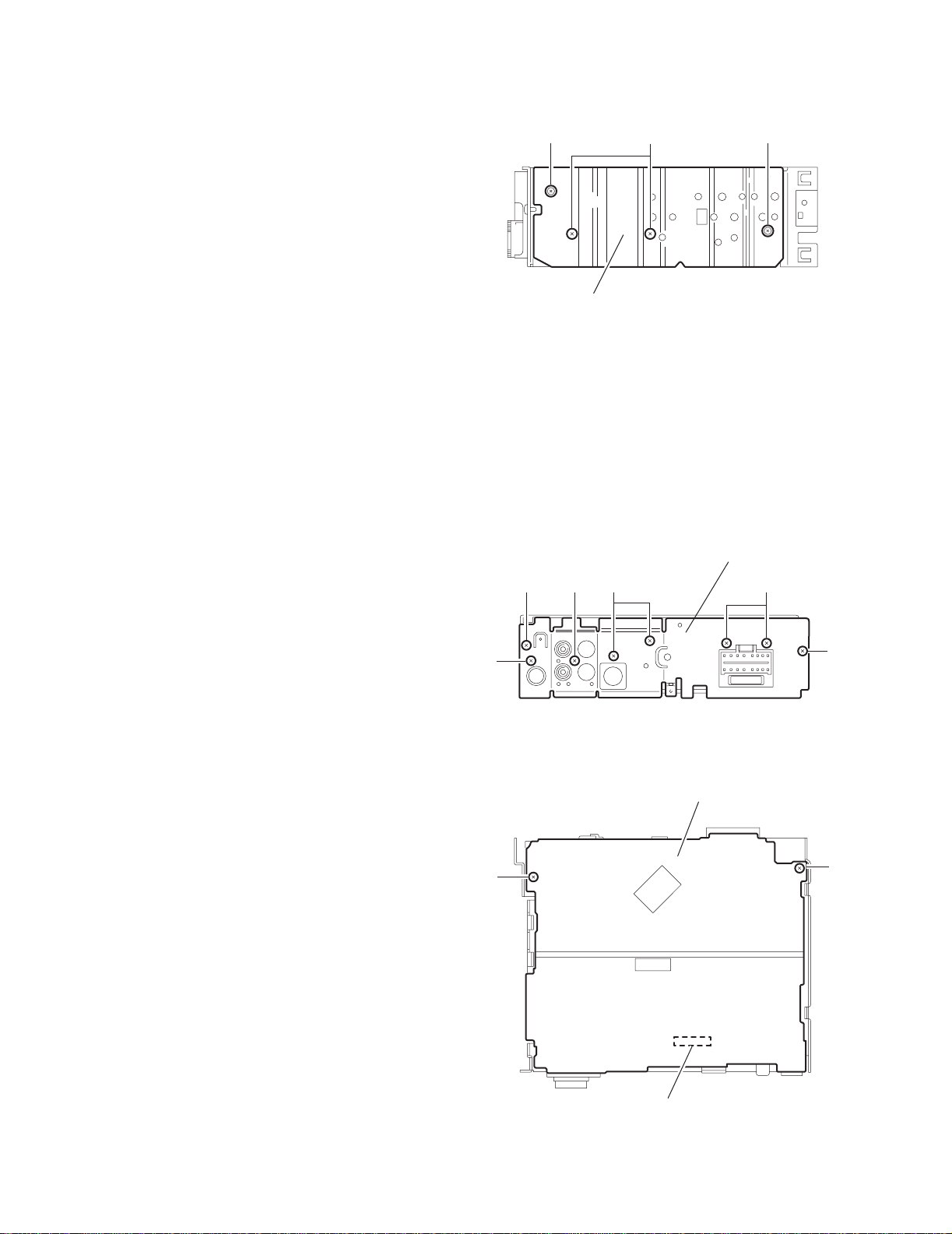
2.1.4 Removing the heat sink
(See Fig.4)
• Prior to performing the following procedure, remove the front
panel assembly.
(1) Remove the two scre ws B and two screws C attaching the
heat sink on the left side of the body, and remove the heat
sink.
2.1.5 Removing the rear panel
(See Fig.5)
• Prior to performing the following procedure, remove the front
panel assembly and bottom cover.
(1) Remove the two screws D, three screws E and three
screws F attaching the rear panel on the back of the body.
CB C
Heat sink
Fig.4
2.1.6 Removing the main board
(See Fig.6)
• Prior to performing the following procedure, remove the front
panel assembly, bottom cover, front chassis, heat sink and
rear panel.
(1) Remove the two screws G attaching the main board on the
top chassis.
(2) Disconnect the connectors CP701 on the main board from
the cassette mechanism assembly.
E
G
D
Rear panel
EFF
D
Fig.5
Main board assembly
G
1-4 (No.49825)
CP701
Fig.6
Page 5
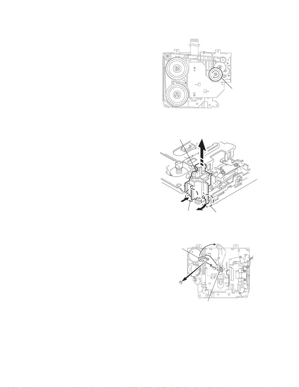
2.1.7 Removing the cassette mechanism assembly
(See Fig.7)
• Prior to performing the following procedure, remove the front
panel assembly, bottom cover, front chassis, heat sink, rear
panel and main board.
(1) Remove the four screws H attaching the cassette mecha-
nism assembly from the top chassis.
2.1.8 Removing the mecha bo ar d
(See Fig.8)
• Prior to performing the following procedure, remove the front
panel assembly, bottom cover, front chassis, heat sink, rear
panel, main board and cassette mechanism assembly.
(1) Disconnect the wire from the connectors CN402 and
CN403 on the mecha board.
(2) Remove the screw J attaching the mecha board.
KS-FX621
Cassette mechanism assembly
H
H
H H
Top chassis
Fig.7
CN402
J
2.1.9 Removing the front board
(See Figs.9 to 11)
• Prior to performing the following procedure, remove the front
panel assembly.
(1) Remove the four screws L attaching the rear cover on the
back of the front panel assembly. (See fig.9)
(2) Release the eleven joints f, the front panel and the rear
cover become separate. (See fig.10)
(3) Remove the front board from the front panel assembly.
(See fig.11)
K
K
K K
Fig.9
CN401
Front panel assembly
Joint h
LCD & Key control board
Fig.8
Joint h
Joint h
Fig.10
CN403
Joint h
Rear cover
Fig.11
(No.49825)1-5
Page 6
KS-FX621
r
2.2 CD Mechanism Assembly
REFERENCE:
Prior to performing the following procedures, turn the mode
gear on the bottom of the body until the respective part comes
to the EJECT position (Refer to Fig.1).
2.2.1 Removing the cassette guide
(See Fig.2)
(1) Turn the mode gear to set to RVS play or subsequent
mode.
(2) Remove the casse tte guide from the main chassis while re-
leasing each two joint tabs a in the direction of the arrow.
Mode gea
Fig.1
Cassette guide
2.2.2 Removing the load arm
(See Fig.3)
(1) Remove the E-washer attaching the load arm.
(2) Move the load arm in the direction of the arrow and release
the joint b on the cassette catch.
Load arm
E-washer
Tab a
Tab a
Fig.2
Joint b
Fig.3
1-6 (No.49825)
Page 7
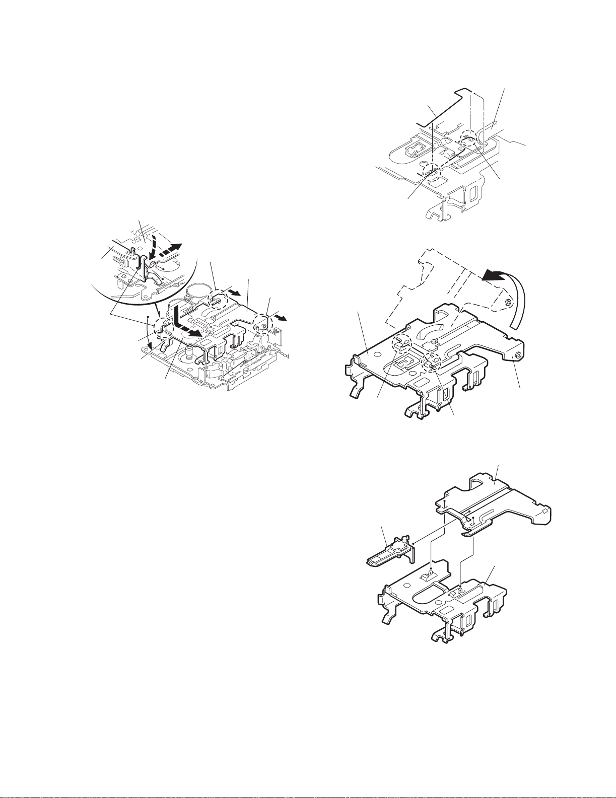
2.2.3 Removing the cassette hanger assembly / cassette holder
y
(See Fig.4 to 7)
(1) Check the mode is set to EJECT. Push down the front part
of the cassette holder and move in the directi on of the arrow to release the joint c.
(2) Move the rear part of the cassette hanger assembly in the
direction of the arrow to release it from the two joint bosses
d.
(3) Release the holder stabilizer spring from the hooks e and
f, then pull out from the cassette hanger assembly.
(4) Bring up the rear side of the cassette hanger assembly to
release the joint g and h.
(5) Pull out the cassette catch from the cassette hanger as-
sembly.
Cassette holder assembly
KS-FX621
Cassette hanger assembly
Cassette stabilizer spring
Hook f
Hook e
Fig.5
Side bracket
Joints c
Cassette holder assembly
Fig.4
Boss d
Cassette hanger
assembly
Boss d
assette holder
ssembly
Cassette hanger assembl
Hook g
Hook h
Fig.6
Cassette hanger assembly
Cassette catch
Cassette holder assembly
Fig.7
(No.49825)1-7
Page 8
KS-FX621
2.2.4 Removing the side bracket assembly
(See Fig.8 to 10)
(1) Remove the screw A attaching the side bracket assembly.
(2) Detach the front side of the side bracket assembly upward
and pull out forward to release the joint i and j in the rear.
CAUTION:
When reassembling, make sure that the boss k of the main
chassis is set in the notch of the load rack under the side
bracket assembly. Do not reattach the load rack on the boss k.
CAUTION:
After reattaching the side bracket assembly, confirm operation.
Side bracket assembly
Joint i
Side bracket assembly
Joint i
Joint j
Load rack
A
Joint j
Boss k
Fig.9
Side bracket assembly
Fig.8
Boss k
Load rack
1-8 (No.49825)
Fig.10
Page 9
2.2.5 Removing the pinch arm (F) assembly
r
r
(See Fig.11 and 12)
(1) Remove the polywasher and pull out the pinch arm (F) as-
sembly.
(2) Remove the compulsion spring.
KS-FX621
Pinch arm (F) assembly
Polywasher
Compulsion spring
Polywasher
Pinch arm
(R) assembly
2.2.6 Removing the pinch arm (R) assembly
(See Fig.11 and 13)
(1) Remove the polywasher and pull out the pinch arm (R) as-
sembly.
Pinch arm
(R) assembly
Pinch arm
(F) assembly
Fig.11
Polywashe
Polywashe
Fig.12
Joint l
Joint l
Slide chassis
assembly
Fig.14
Fig.13
2.2.7 Removing the slide chassis assembly
(See Fig.14 and 15)
REFERENCE:
It is not necessary to remove the head and the tape guide.
(1) Move the slide chassis assembly in the direction of the ar-
row to release the two joints l and remove from the main
chassis.
(2) Remove the rack link.
CAUTION:
When reassembling, first reattach the rack link, and next fit the
boss m and hook n of the slide chassis assembly to the hole
of the main chassis, and engage the two joints l.
Head
Tape guide
Boss m
Rack link
Hook
n
Fig.15
(No.49825)1-9
Page 10
KS-FX621
2.2.8 Removing the head / tape guide
(See Fig.16 and 17)
REFERENCE:
It is not necessary to remove the slide chassis assembly.
(1) Remove the band attaching the wire to the head.
(2) Remove the two screws B, the head and the head support
spring.
(3) Remove the pinch arm spring from the tape guide.
(4) Remove the tape guide and the pinch spring arm.
CAUTION:
When reattaching the pinch arm spring, set both end of it to the
pinch spring arm ( remarked o).
CAUTION:
When reattaching the head, set the wires into the groove of the
tape guide (Fig.16).
Slide chassis assembly
B
Pinch arm spring
Head
Head support spring
Tape guide
o
B
Pinch spring arm
o
Head
Fig.16
2.2.9 Removing the flywheel assembly (F) & (R)
(See Fig.18 and 19)
REFERENCE:
It is not necessary to remove the slide chassis assembly.
(1) Remove the belt at the bottom.
(2) Remove the two polywashers on the upper side.
(3) Pull out each flywheel assembly downward.
Flywheel assembly (F)
Tape guide
Belt
Slid chassis assembly
Fig.17
Polywasher
Polywasher
Flywheel assembly (F)
Flywheel assembly (R)
1-10 (No.49825)
Flywheel assembly (R)
Fig.19
Fig.18
Page 11

2.2.10 Disassembling the flywheel assembly (F )
r
(See Fig.20 and 21)
(1) Push and turn counterclockwise the spring holder (F) to re-
lease the three joints p on the bottom of the flywheel.
(2) The spring holder (F), the TU spring and the friction gear
play come off.
(3) Remove the polywasher and felt.
KS-FX621
Polywasher
Spring holder (F)
TU spring
Flywheel assembly (F)
Joints p
Joint p
Fig.20
2.2.11 Disassembling the flywheel assembly (R)
(See Fig.20 and 22)
(1) Push and turn clockwise the spring holder (R) to release
the three joints q on the bottom of the flywheel.
(2) The spring holder (R), the FF spring and the friction gear
FF come off.
(3) Remove the polywasher and the felt.
Polywasher
Spring holder (R)
FF spring
Flywheel assembly (R)
Joints q
Joint q
Friction gear play
Felt
Flywheel assembly (F)
Fig.21
FFC pad
C
Joint
Friction gear FF
Felt
Flywheel assembly (R)
Fig.22
2.2.12 Removing the reel board
(See Fig.23 and 24)
(1) Remove the two screws C attaching the reel board.
(2) Move the reel board in the direction of the arrow to release
the joint r.
(3) Unsolder the wires if necessary.
CAUTION:
When reattaching, confirm operation of the MODE switch and
the ST-BY switch.
The mode position between EJECT and ST-BY is optimum for
reattaching.
Connect the card wire extending from the reel board to the
FFC pad before reattaching the reel board.
C
Reel board
Fig.23
FFC pad
CT-1 switch
MODE switch
ST-BY switch
Soldering
Fig.24
(No.49825)1-11
Page 12

KS-FX621
2.2.13 Removing the gear base arm / gear base link assembly
(See Fig.25 to 27)
(1) Move the gear base arm in the direction of the arrow.
(2) Insert a slotted screwdriver to the gear base spring under
the gear base arm, and release the gear base arm upward
from the boss on the gear base assembly.
(3) Remove the gear base arm from the main chassis while re-
leasing the two joints s.
(4) Move the gear base link assemby in the direction of the ar-
row to release the two joints t.
REFERENCE:
When reattaching the gear base arm, make sure that the boss
on the gear base assembly is inside the gear base spring.
Joint t
Gear base arm
Joints s
Hook u
FFC pad
Hook u
2.2.14 Removing the FFC pad
(See Fig.27 and 29)
(1) Push each joint hook u of the FFC pad and remove toward
the bottom.
Gear base
link assembly
Joint t
Gear base spring
Gear base link assembly
Fig.25
Gear base arm
Screwdriver
Fig.26
Gear base arm
1-12 (No.49825)
FFC pad
Fig.27
Page 13

KS-FX621
r
r
2.2.15 Removing the mode gear
(See Fig.28 and 31)
(1) Remove the polywasher on the bottom and pull out the
mode gear.
2.2.16 Removing the mode switch actuator
(See Fig.28, 29 and 31)
(1) Pull out the mode switch actuator at the bottom.
REFERENCE:
When reattaching the mode switch actuator to the main chassis, make sure to set on the shaft and insert v into the slot w.
2.2.17 Removing the direction link / direction plate
(See Fig.29 to 31)
(1) Remove the polywasher attaching the direction link.
(2) Bring up the direction link to release the three joints x, y
and z at a time.
(3) Move the direction plate in the direction of the arrow to re-
lease the two joints a'.
REFERENCE:
When reattaching the direction plate, engage the two joints a'
and move in the direction of the arrow (Refer to Fig.30).
REFERENCE:
When reattaching the direction link, move the direction plate in
the direction of the arrow and engage the three join t x, y and
z at a time (Refer to Fig.31).
2.2.18 Removing the mode rack assembly
(See Fig.29 and 30)
(1) Move the mode rack assembly in the direction of the arrow
to release the two joints b' and the joint c'.
REFERENCE:
When reattaching, set the two b' Eon the bottom of the mode
rack assembly into the slots of the main chassis and move in
the direction of the arrow (See Fig.30).
Mode switch actuator
Direction plate
Direction plate
Direction link
Fig.28
Slot w
Mode rack assembly
Joints a'
Joint z
Direction link
Polywasher
Joint y
Fig.29
Joint x
Direction plate Mode rack assembly
Joint b'
Mode gear
Polywashe
Joint b'
Joint c'
Joints a'
Fig.30
Direction link
Mode switch actuator
Polywasher
v
Mode gea
Direction plate
Mode rack assembly
Fig.31
(No.49825)1-13
Page 14

KS-FX621
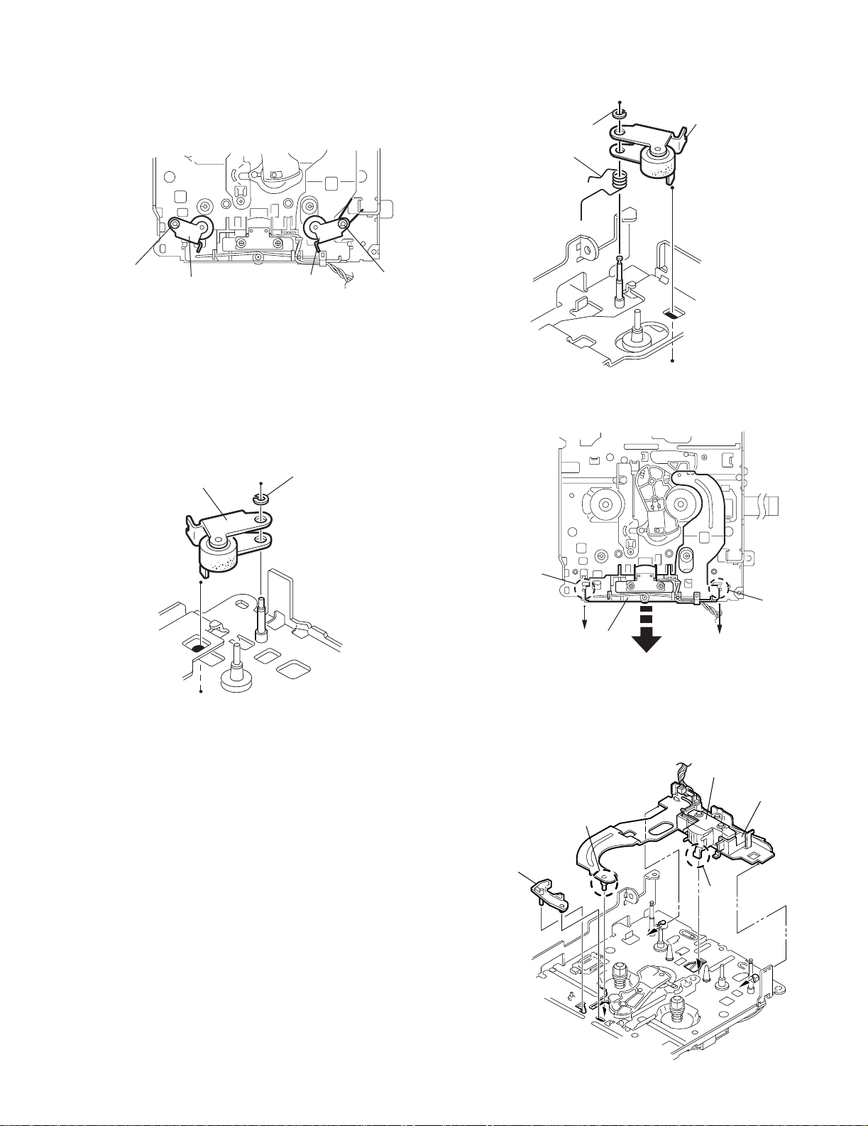
2.2.19 Removing the gear base assembly / take up gear / reflector gear
(See Fig.32 to 34)
(1) Push in the pin d' of the gear base assembly on the upper
side of the body and move the reflector gear toward the
bottom, then pull out.
(2) Remove the polywasher on the bottom and pull out the
take up gear.
(3) Move the gear base assembly in the direction of the arrow
to release it from the two slots e' of the main chassis.
REFERENCE:
The parts are damaged when removed. Please replace with
new ones.
Slot e'
Gear base assembly
Pin d'
Slot e'
Fig.32
2.2.20 Removing the reel driver / reel spindle
(See Fig.34)
(1) Draw out the reel driver from the shaft on the main chassis
and remove the reel driver spring and the reel spindle respectively.
CAUTION:
The reel driver is damaged when removed. Please replace
with a new one.
Polywasher
Reflector gear
Reel driver
Reel driver spring
Reel spindle
Take up gear
Fig.33
Reel driver
Reel driver spring
Reel spindle
Gear base assembly
1-14 (No.49825)
Main chassis
Reflector gear
Slots e
Take up gear
Polywasher
Fig.34
Page 15

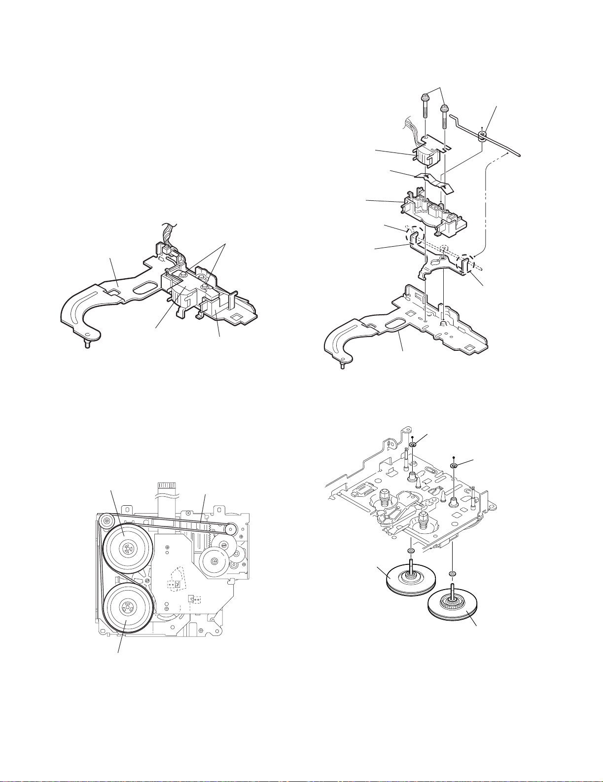
2.2.21 Removing the side bracket assembl y
(See Fig.35 to 39)
(1) Remove the eject cam plate spring.
(2) Push the joint f' through the slot to remove the load rack
downward.
(3) Move the eject cam limiter in the direction of the arrow to
release it from the boss g'of the side brack et assembly and
from the two joints h'.
(4) Move the eject cam plate in the direction of the arrow to re-
lease the joint i'.
CAUTION:
When reassembling, confirm operation of each part before reattaching the eject cam plate spring.
Joint f'
Side bracket
assembly
Boss g'
Eject cam limiter
Joint h'
Eject cam plate
Fig.37
Side bracket assembly
Boss g'
KS-FX621
Joint h'
Eject cam plate spring
Side bracket assembly
Boss g'
Joint h'
Fig.35
Eject cam limiter
Joint f'
Load rack
Joint h'
Eject cam plate
Eject cam plate
Joint i'
Fig.38
Side bracket assembly
Joint i’
Fig.39
Fig.36
Load rack
(No.49825)1-15
Page 16

KS-FX621
r
2.2.22 Removing the main motor assembly / sub motor assembly
(See Fig.40 to 42)
(1) Remove the belt at the bottom.
(2) Remove the polywasher and pull out the mode gear.
(3) Pull out the reduction gear (B).
(4) Remove the polywasher and pull out the reduction gear
(A).
(5) Remove the two screws D attaching the main motor as-
sembly.
(6) Remove the two scre ws E attaching the sub motor assem-
bly.
(7) Unsolder the wires on the reel board if necessary.
CAUTION:
When reassembling, adjust the length of the wires extending
from the sub motor asswmbly by attaching them to the side of
the sub motor assembly with the wires extending from the
main motor assembly using a spacer.
Belt
Reduction gear (B)
Reduction gear (B)
Mode gear
Polywasher
Fig.40
Polywasher
D
E
Main motor
assembly
Reduction
gear (A)
Polywashe
Sub motor
assembly
E
Spacer
Main motor assembly
Reduction gear (A)
D
Main motor assembly
Sub motor assembly
Fig.41
1-16 (No.49825)
Sub motor assembly
Fig.42
Spacer
Page 17

SECTION 3
Adjustment
3.1 Adjustment method
Test instruments reqired for adjustment Standard volume position
1. Digital oscilloscoe(100MHz)
2.Frequency counter meter
3.Electric voltmeter
4.Wow & flutter meter
5.Test tapes
VT724.......................for DOLBY level measurement
VT739............For playback frequency measurement
VT712....For wow flutter & tape speed measurement
VT703.....................For head azimuth measurement
6.Torque gauge...................Cassette type for CTG-N
(Mechanism adjustment)
Measuring conditions(Amplifier section)
Balance and Bass, Treble volume, Fader
: Center(Indication"0")
Loudness, Dolby NR, Sound, Cruise : Off
Volume position is about 2V at speaker output with
following conditions, Playback the test tape VT721.
AM mode 999kHz/62dB, INT/400Hz, 30%
modulation signal on recieving.
FM mono mode 97.9MHz/66dB, INT/400Hz, 22.5kHz
deviation pilot off mono
FM stereo mode 1kHz, 67.5kHz dev.pilot 7.5kHz dev
Output level 0dB (1 V,50 /open terminal)
KS-FX621
Power supply voltage.............. DC14.4V(11V to 16V allowance)
Load impedance............ 4 (4 to 8 allowance)
Line out level/Impedance..............1.0V/20k load (250 nWb/m)
Frequency band
Band
FM
AM
87.5 MHz to 108.0MHz
522 kHz to 1620 kHz
MW
LW
144 kHz to 279 kHz
(No.49825)1-17
Page 18

KS-FX621
Information for using a car audio service jig
1. We're advancing efforts to make our extension cords common for all car audio products.
Please use this type of extension cord as follows.
2. As a U-shape type top cover is employed, this type of extension cord is needed to check operation of the
mechanism assembly after disassembly.
3. Extension cord : EXTKSRT002-18P ( 18 pin extension cord ) For connection between mechanism assembly
and main board.
4. Check for mechanism driving section such as motor ,etc.
D
i
sassembl
1. Remove the front panel assembly.
2. Remove the bottom cover.
3. Remove the front chassis.
4. Remove the rear panel.
5. Remove the heat sink.
6. Remove the main board.
7. Reattach the heat sink with two screw B. (Refer to Disassembly method.)
8. Install the front chassis and front panel assmbly.
9. Confirm that current is being carried by connecting an extension cord jig.
Note
Available to connect to the CJ701 connector when installing the front panel.
y met
hod
CAUTION :
Be sure to attach a heat sink on the power amplifier IC of a main board when supplying the power.
If voltage is applied without attaching the heat sink, the power amplifier IC will be destroyed by heat.
To
Cassette mechanism
Extension cord
EXTKSRT002-18P
To
Main board
EXTKSRT002-18P
Cassette mechanism
1-18 (No.49825)
Front panel assembly
Main board
Page 19

Arrangement of adjusting & test points
A
Cassette mechanism
(Surface)
Motor assembly
Tape speed adjust
KS-FX621
Azimuth screw
(Forward)
Playback head
Head section view
Azimuth screw B
(Reverse)
Azimuth screw B
(Reverse)
Playback head
Azimuth screw A
(Forward)
(No.49825)1-19
Page 20

KS-FX621
Item
Head
1.
azimuth
adjustment
Conditions
Test tape:
SCC-1659
VT703(10kHz)
Adjustment and Confirmation methods
Head height adjustment
Adjust the azimuth directly. When you
adjust the height using a mirror tape,
remove the cassette housing from the
mechanism chassis. After installing the
cassette housing, perform the azimuth
adjustment.
Load the SCC-1659 mirror tape. Adjust with
1.
height adjustment screw A and azimuth
adjustment screw B so that line A of the
mirror tape runs in the center between Lch
and Rch in the reverse play mode.
After switching from REV to FWD then to
2.
REV, check that the head position set in
procedure 1 is not changed. (If the position
has shifted, adjust again and check.)
Adjust with azimuth adjustment screw B so
3.
that line B of the mirror tape runs in the
center between Lch and Rch in the forward
play mode.
Head azimuth adjustment
Load VT724 (1kHz) and play it back in
1.
the reverse play mode.
Set the Rch output level to max.
Load VT703 (10kHz) and play it back in
2.
the forward play mode. Adjust the Rch
and Lch output levels to max, with
azimuth adjustment screw B. In this case,
the phase difference should be within 45 .
Engage the reverse mode and adjust the
3.
output level to max, with azimuth
adjustment screw C.
(The phase difference should be 45 or
more.)
When switching between forward and
4.
reverse modes, the difference between
channels should be within 3dB. (Between
FWD L and R, REV L and R.)
S.Values Adjust
A line
Head shield
The head is at low position
during.
B line
Head shield
The head is at High position
during REV.
Output
level:
Maximum
PBHead
FWD Adj B
REV Adj C
(0 ) (45 )
HEIGHT Adj A
phase
Tape speed
2.
and wow
flutter
confirmation
Play back
3.
frequency
response
confiramation
1-20 (No.49825)
When VT721 (315Hz) is played back,
5.
the level difference between channels
should be within 1.5dB.
Test tape: VT712
(3kHz)
Test tape: VT724
(1kHz)
VT739
(63Hz / 1kHz / 10kHz)
The tuner section is of an adjustment-freedesign. In case the tuner is in trouble, replace the tuner pack.
Check to see if the reading of the F, counter /
1.
wow flutter meter is within 3015Hz to 3045Hz
(FWD/ REV), and less than 0.35% (JIS RMS).
In case of out of specification, adjust the
2.
motor with a built-in volume resistor.
Play test tape VT724, and set the volume
1.
position at 2V.
Play test tape VT739 and confirm.
2.
1kHz / 10kHz: -1 3dB,
1kHz / 63Hz: 0 3dB,
When 10kHz is out of specification, it will be
3.
necessary to read adjust the azimuth.
Tape speed:
3015Hz
to 3045Hz
Wow
flutter: less
than 0.35%
Speaker out
1kHz / 63Hz
: 0 3db
1kHz / 10kHz
: -1 3db
Built-in volume
resistor
Page 21

4.1 CXA2559Q (IC401) : Head amp.
•Pin layout
KS-FX621
SECTION 4
Description of major ICs
• Block diagram
1
10
31
32
33
34
35
36
37
38
39
40
45k
30
7k/12k
300k
300k
7k/12k
30
21
F2
30k
30k
F1
29
-
+
+
-
28
100k
X1
X1
100k
27
T2
T1
26
TAPE EQ
FWD/RVS
LPF
25
BIAS
MUTE
Vcc
+
-
F3
+
+
24
-
-
23
24dB
24dB
22
MS MODE
MS ON/
OFF
DET
21
20
19
18
17
16
15
14
13
12
11
1
2
3
4
5
6
7
8
9
10
(No.49825)1-21
Page 22

KS-FX621
c
Y
Y
Y
Y
4.2 HD74HC126P (IC801) : Changer control
• Pin arrangement • Pin function
11C
21A
31Y
14
13
12
Vc
4C
4A
Input Output
CA Y
LX Z
HL L
HH H
• Block diagram
42C
52A
62Y
7GND
11
10
4Y
3C
9
3A
8
3Y
( TOP VIEW )
1A
1
1C
2A
2
2C
3A
3C
4A
4C
3
4
1-22 (No.49825)
Page 23

4.3 KIA7810PI (IC902) : Regulator
•Pin layout
1 2 3
• Block diagram
KS-FX621
1 INPUT
R4 R18
Q12
R5
Z1
R6
R7
R1
Q1
Q13
R10 R3
Q8
Q10
Q5
Q7
R8
R2
Q6
Q2
R15
Q14
C1
R14
Q4
Q9
R16
R9
Q15
Q3
Q11
R13
R21
R17
Q16
R12
R19
Q17
R11
3 OUTPUT
R20
2 GND
(No.49825)1-23
Page 24

KS-FX621
4.4 LC72366-9B41 (IC701) : Micon
• Pin layout
65 ~ 80
64 ~ 41
40 ~ 25
1 ~ 24
• Pin function
Pin No. Symbol I/O Function
1 XIN I 4.5MHz crystal oscillation
2 TEST2 - Connect to ground
3 J-BUS SI I J-BUS signal data input (to 74HC126)
4 J-BUS SO O J-BUS signal data output (to 74HC126)
5 J-BUS SCK O J-BUS output clock signal (to 74HC126)
6 J-BUS I/O I/O J-BUS I/O control ie. "H" = "O", "L" = "I" (to 74HC126)
7NC-No use
8 LCD SO O LCD driver data output (to LC75823E pin 64)
9 LCD SCK O LCD driver clock signal (to LC75823E pin 63)
10 LCD CE O LCD driver chip enable port (to LC75823E pin 62)
11 NC - No use
12 SDA O E. volume data output (to TEA632 0T pin 1)
13 SCL O E. volume clock output (to TEA6320T pin 32)
14 NC - No use
15 TUNER_ILL O Connect to LED (of TUNER button )
16 TAPE_ILL O Connect to LED (of TAPE button)
17 CD_ILL O Connect to LED (of CD button)
18 DIMMER O Connect to display lamp supply
19~24 NC - No use
25 KS1 O Output for initial setting diode matrix
26 KS0 O Output for initial setting diode matrix
27 K3 I Input for initial setting diode matrix
28 K2 I Input for initial setting diode matrix
29 K1 I Input for initial setting diode matrix
30 K0 I Input for initial setting diode matrix
31 Vdd - 5V supply
32 TEST I Change key input to test mode
33 FF/REW O Change MS IC input sensitivity (L at FF/REW)
34 SEEK/STOP O IF count REQ and output [H] at seek.and scan
35 MONO O Output [H] at FM forced monoral mode
36 R/T O Output of mode radio / tape (Radio:H.Tape:L)
37 NC - No use
38 POWER ON - Output [H] at power on
39 ACC O Output [H] during [ACC DET] is [H]
40 IFC CONT O IF count control output (To tuner cct)
41 MOTER O Main motor output (Drive:H Stop:L)
42 SUB MOTER+ O Sub motor output (sub motor loading )
43 SUB MOTER- O Sub motor output (sub motor eject)
44 BEEP O Beep on (output f :2.25KHz)
1-24 (No.49825)
Page 25

Pin No. Symbol I/O Function
45 TAPE IN I Detect cassette in SW. [H] at cassette in
46 STAND BY I Detect stand by SW position.
47 REEL I Pulse input
48 MODE I Detect mode position.
49 F/R O Output F/R ( Forward:L Reverse:H)
50 MS IN I Detect MS. [H] at no music.
51 SD/ST I Station detect and FM stereo signal input [H] at SD
52 DETACH I Front panel detect
53 JOG-0 I Rotary encoder input 0
54 JOG-1 I Rotary encoder input 1
55 JBUS INT I J-BUS interrupt (to 74HC126)
56 REMOCON I Remocon input
57 BAND O FM/AM band selection ("H" : FM, "L" : AM)
58 DOLBY O Output DOLBY mode ("H" : DOLBY on)
59 IFRQ/AGC O During FM auto search IF request output 'H' after SD detected.
During AM auto search AGC output ("H" : auto search)
60 MUTE O Muting switch
61 P.SAVE2 I Power save 2 : +B detect
62 LEVEL I Level meter input
63 S.METER I S meter input
64 KEY2 I Key 2 data input (AD)
65 KEY1 I Key 1 data input (AD)
66 KEY0 I Key 0 data input (AD)
67 P.SAVE1 I Power save 1, ACC power detect
68 SNS I Voltage sense
69 NC 70 FM IF COUNT I FM IF counter data input
71 NC 72 NC 73 Vdd - 5V supply
74 NC 75 FM OSC I FM input frequency
76 Vss - Ground
77 NC 78 EO O PLL error output signa l
79 TEST1 - Connect to ground
80 XOUT O 4.5MHz crystal oscillation
KS-FX621
(No.49825)1-25
Page 26

KS-FX621
4.5 LA4743K (IC301) : Power amp.
• Block diagram
IN 1
TAB
IN 2
+
0.22 F
+
0.22 F
11
1
12
Vcc 1/2 Vcc 3/4
6 20
-
+
Protective
circuit
-
+
2200 F 0.022 F
+
9
7
+
OUT 1+
OUT 1-
PWR GND1
8
+
OUT 2+
5
-
OUT 2-
3
PWR GND2
2
ST BY
R.F
47 F
IN 3
PRE GND
IN 4
+5V
ST ON
+
0.22 F
N.C
+
0.22 F
4
Stand by
Switch
Mute
10
+
Ripple
Filter
Mute
22
circuit
3.3 F
+
15
-
+
-
17
19
10K
+
OUT 3+
OUT 3-
Low Level
Mute ON
25
18
21
23
PWR GND3
OUT 4+
OUT 4-
13
14
Protective
circuit
-
+
+
-
ON TIME C
1-26 (No.49825)
22 F
Muting &
16
+
ON Time Control
Circuit
PWR GND4
24
Page 27

4.6 PT6523LQ (IC651) : LCD driver
•Pin layout
48 ~ 33
49
KS-FX621
32
• Block diagram
64
1 ~ 16
17
COMMON
DRIVER
CLOCK
GENERATOR
ADDRESS
DETECTOR
SEGMENT DRIVER & LATCH
SHIFT REGISTER
• Piin function
Pin No. Pin Name I/O Description
1~ 52 SG1 ~ SG52 O Segment Output Pins
53~55 COM1 ~ COM3 O Common Driver Output Pins
56 VDD - Power Supply
57 INH
I Display OFF Control Input Pin
When this pin is "Low", the Display is forcibly turned OFF. (SG1 to SG52, COM1 to COM3 are
set to "LOW"). (See Note 1)
When this pin is set to "High", the Displa is ON.
58 VDD1 I Used for the 2/3 Bias Voltage when the Bias Voltages are provied externally. Connect to VDD2
when 1/2 Bias is used.
59 VDD2 I Used for 1/3 Bi as Voltage when the Bias Voltages are provided externally. Connect to VDD1
when 1/2 Bias is used.
60 VSS - Ground Pin.
61 OSC I/O Oscillation Input /Outout Pin
62 CE I Chip Enable Pin
63 CLK I Synchronization Clock
64 DI I Transfer Data Pin
Note 1:
When INH
= "LOW" : Serial data trensfers can be performed when the display is forcibly OFF.
(No.49825)1-27
Page 28

KS-FX621
4.7 RPM6938-SV4 (IC652) : Remote sensor
• Pin diagram
1 2 3
• Block diagram
AGC
AMP
I/V
conversion
PD
magnetic shield
BPF
fo
trimming
circuit
Detector
4.8 LB1641 (IC402) : DC motor driver
• Pin layout • Truth table
GND
OUT1
P1
VZ
IN1
IN2
VCC1
VCC2
P2
OUT2
1
2
3
4
5
6
7
8
9
10
Input Output Mode
IN1 IN2 OUT1 OUT2
0000 Brake
1010 CLOCKWISE
0 1 0 1 COUNTER-CLOCKWISE
1100 Brake
Vcc
Comp
Vcc
22k
Rout
GND
1-28 (No.49825)
Page 29

4.9 TEA6320T-X (IC161) : E.volume
•Pin layout
SDA
1
GND
TL
B2L
B1L
IVL
ILL
QSL
IDL
MUTE
ICL
IMD
IBL
IAL
2
3
4
5
6
7
8
9
10
11
12
13
14
15
16
CD-CH
TAPE
TUNER
OUTLR
OUTLF
• Block diagram
10 8 9 7 6
32
31
30
29
28
27
26
25
24
23
22
21
20
19
18
17
SCL
VCC
OUTRR
OUTRF
TR
B2R
B1R
IVR
ILR
QSR
IDR
Vref
ICR
CAP
IBR
IAR
KS-FX621
5
12
21
31
2
19
POWER
SUPPLY
VOLUME 1
+20 to -31 dB
LOUDNESS
LEFT
16
15
13
11
14
22
20
SOURCE
SELECTOR
VOLUME 1
+20 to -31 dB
LOUDNESS
RIGHT
18
17
23 25 24 26 27 28
• Pin functions
Pin No. Symbol I/O Functions
1 SDA I/O Serial data input/output.
2 GND - Ground.
3 OUTLR O output left rear.
4 OUTLF O output left front.
5 TL I Treble control capacitor left channel or
input from an external equalizer.
6 B2L - Bass control capacitor left channel or
output to an external equalizer.
7 B1L - Bass control capacitor left channel.
8 IVL I Input volume 1. left control part.
9 ILL I Input loudness. left control part.
10 QSL O Output source selector. left channel.
11 IDL - Not used
12 MUTE - Not used
13 ICL I Input C left source.
14 IMO - Not used
15 IBL I Input B left source.
16 IAL I Input A left source.
BASS
LEFT
+15 dB
LOGIC
BASS
RIGHT
+15 dB
VOLUME 2
0 to 55 dB
BALANCE
FENDER REAR
VOLUME 2
0 to 55 dB
BALANCE
FENDER FRONT
HC BUS
REC
3
4
32
TREBLE
LEFT
+12 dB
MUTE
FUNCTION
ZERO CROSS
DETECTOR
1
VOLUME 2
TREBLE
RIGHT
+12 dB
0 to -55dB
BALANCE
FENDER FRONT
VOLUME 2
0 to -55dB
BALANCE
FENDER REAR
29
30
Pin No. Symbol I/O Functions
17 IAR I Input A right source.
18 IBR I Input B right source.
19 CAP - Electronic filtering for supply.
20 ICR I Input C right source.
21 Vre f - Reference voltage (0.5Vcc)
22 IDR - Not used
23 QSR O Output source selector right channel.
24 ILR I Input loudness right channel.
25 IVR I Input volume 1. right control part.
26 B1R - Bass control capacitor right channel
27 B2R O Bass control capacitor right channel or
output to an external equalizer.
28 TR I Treble control capacitor right channel or
input from an external equalizer.
29 OUTRF O Output right front.
30 OUTRR O Output right rear.
31 Vcc - Supply voltage.
32 SCL I Serial clock input.
(No.49825)1-29
Page 30

KS-FX621
4.10 AN80T05 (IC901) : Regulator
• Terminal layout & Block diagram
Reference Voltage
Thermal
Protection
ASO & Peak
Current Protection
Pre
Drive
Pre
Drive
AMP
Out
AMP
Out
Pre
Drive
123456789101112
ILL
10V
MODE2 MODE1 STB VDD
5.6V
AMP VCC ANT COM
• Pin function
Pin No. Symbol Function
1 ILL 10V power supply for illumination.
2 MODE2 When 5V is input,becomes AM. and the antenna output is turned on.
3 MODE1 When 5V is input,becomes AM. and the output of FM is switched.
4 STB When 5V is input outputs to ILL,COM,and AMP. It is 0V usually.
5 VDD 5.6V power supply.
6 AMP Power supply supply to remote amplifier
7 VCC Back up. conn ects with ACC with it.
8 ANT Psower supply supply to auto antenna.
9 COM 8.7V power supply.
10 AM The power supply of 8.7V to AM.
11 FM The power supply of 8.7V to FM.
12 GND Ground
Pre
Drive
8.7VAM8.7VFM8.7V
Pre
Drive
GND
1-30 (No.49825)
Page 31

KS-FX621
(No.49825)1-31
Page 32

KS-FX621
VICTOR COMPANY OF JAPAN, LIMITED
AV & MULTIMEDIA COMPANY MOBILE ENTERTAINMENT CATEGORY 10-1,1chome,Ohwatari-machi,Maebashi-city,371-8543,Japan
(No.49825)
Printed in Japan
200303WPC
 Loading...