

Page 1
49825200303
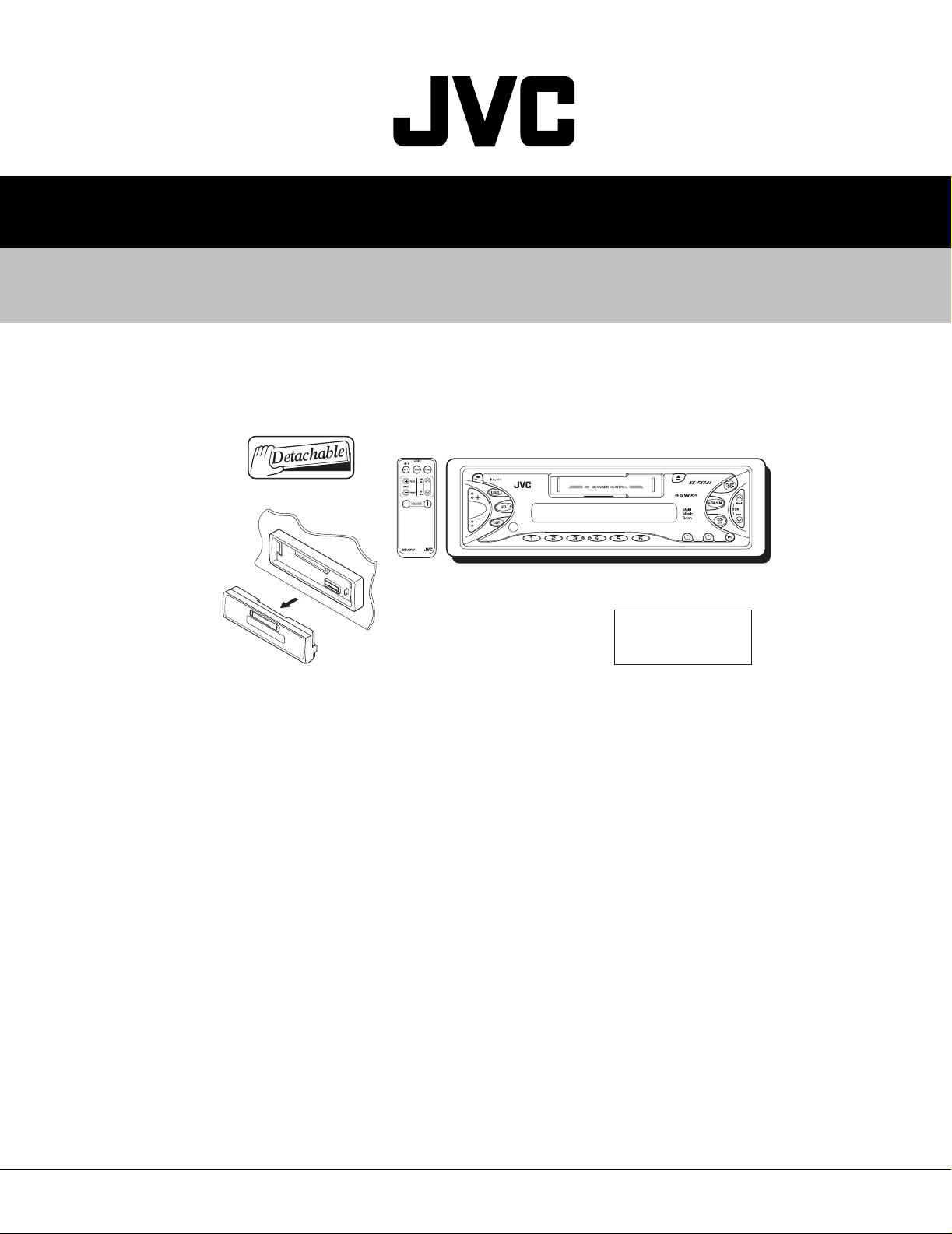
KS-FX621
SERVICE MANUAL
CASSETTE RECEIVER
KS-FX621
11
RPT
1097
12
8
MO
RND
S
C
M
MODE
Area Suffix
U ------ Other Areas
TABLE OF CONTENTS
1 Safety precaution . . . . . . . . . . . . . . . . . . . . . . . . . . . . . . . . . . . . . . . . . . . . . . . . . . . . . . . . . . . . . . . . . . . . . 1-2
2 Disassembly method . . . . . . . . . . . . . . . . . . . . . . . . . . . . . . . . . . . . . . . . . . . . . . . . . . . . . . . . . . . . . . . . . . 1-3
3 Adjustment. . . . . . . . . . . . . . . . . . . . . . . . . . . . . . . . . . . . . . . . . . . . . . . . . . . . . . . . . . . . . . . . . . . . . . . . . . 1-17
4 Description of major ICs. . . . . . . . . . . . . . . . . . . . . . . . . . . . . . . . . . . . . . . . . . . . . . . . . . . . . . . . . . . . . . . 1-21
COPYRIGHT © 2003 VICTOR COMPANY OF JAPAN, LTD.
No.49825
2003/03
Page 2

KS-FX621
SECTION 1
Safety precaution
CAUTION
Burrs formed during molding may be left over on some parts of the chassis. Therefore, pay attention to such burrs in
the case of preforming repair of this system.
1-2 (No.49825)
Page 3
SECTION 2
Disassembly method
2.1 Main body
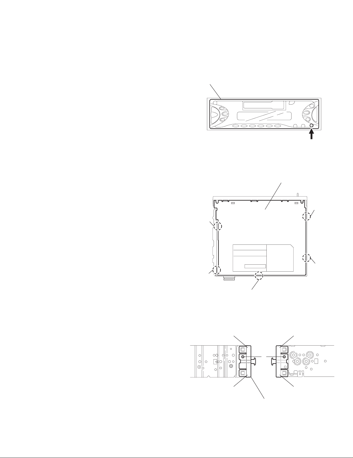
2.1.1 Removing the front panel assembly
(See Fig.1)
(1) Press the release button and remove the front panel as-
sembly.
2.1.2 Removing the bottom cover
(See Fig.2)
• Prior to performing the following procedure, remove the front
panel assembly.
(1) Turn the body upside down.
(2) Insert a screwdriver under the joints to release the two
joints a on the left si de, the two joints b on the right side and
the joint c on the back of the body, then remove the bottom
cover from the body.
CAUTION:
When releasing the joint c using a screwdriver, do not damage
the main board.
Front panel assembly
Joint a
Fig.1
Bottom cover
KS-FX621
Release button
Joint
b
2.1.3 Removing the front chassis
(See Fig.3)
• Prior to performing the following procedure, remove the front
panel assembly and bottom cover.
(1) Remove the screw A on each side of the body.
(2) Release the two joints d and the two joints e on the sides,
then remove the front chassis toward the front.
Joint a
Joint c
Fig.2
Joint d
Joint e
A
Joint d Joint e
Front chassis
Fig.3
Joint b
(No.49825)1-3
Page 4
KS-FX621
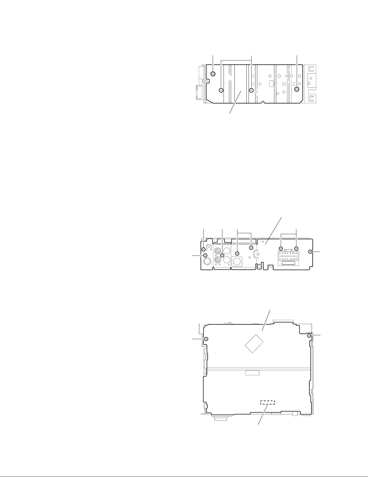
2.1.4 Removing the heat sink
(See Fig.4)
• Prior to performing the following procedure, remove the front
panel assembly.
(1) Remove the two scre ws B and two screws C attaching the
heat sink on the left side of the body, and remove the heat
sink.
2.1.5 Removing the rear panel
(See Fig.5)
• Prior to performing the following procedure, remove the front
panel assembly and bottom cover.
(1) Remove the two screws D, three screws E and three
screws F attaching the rear panel on the back of the body.
CB C
Heat sink
Fig.4
2.1.6 Removing the main board
(See Fig.6)
• Prior to performing the following procedure, remove the front
panel assembly, bottom cover, front chassis, heat sink and
rear panel.
(1) Remove the two screws G attaching the main board on the
top chassis.
(2) Disconnect the connectors CP701 on the main board from
the cassette mechanism assembly.
E
G
D
Rear panel
EFF
D
Fig.5
Main board assembly
G
1-4 (No.49825)
CP701
Fig.6
Page 5
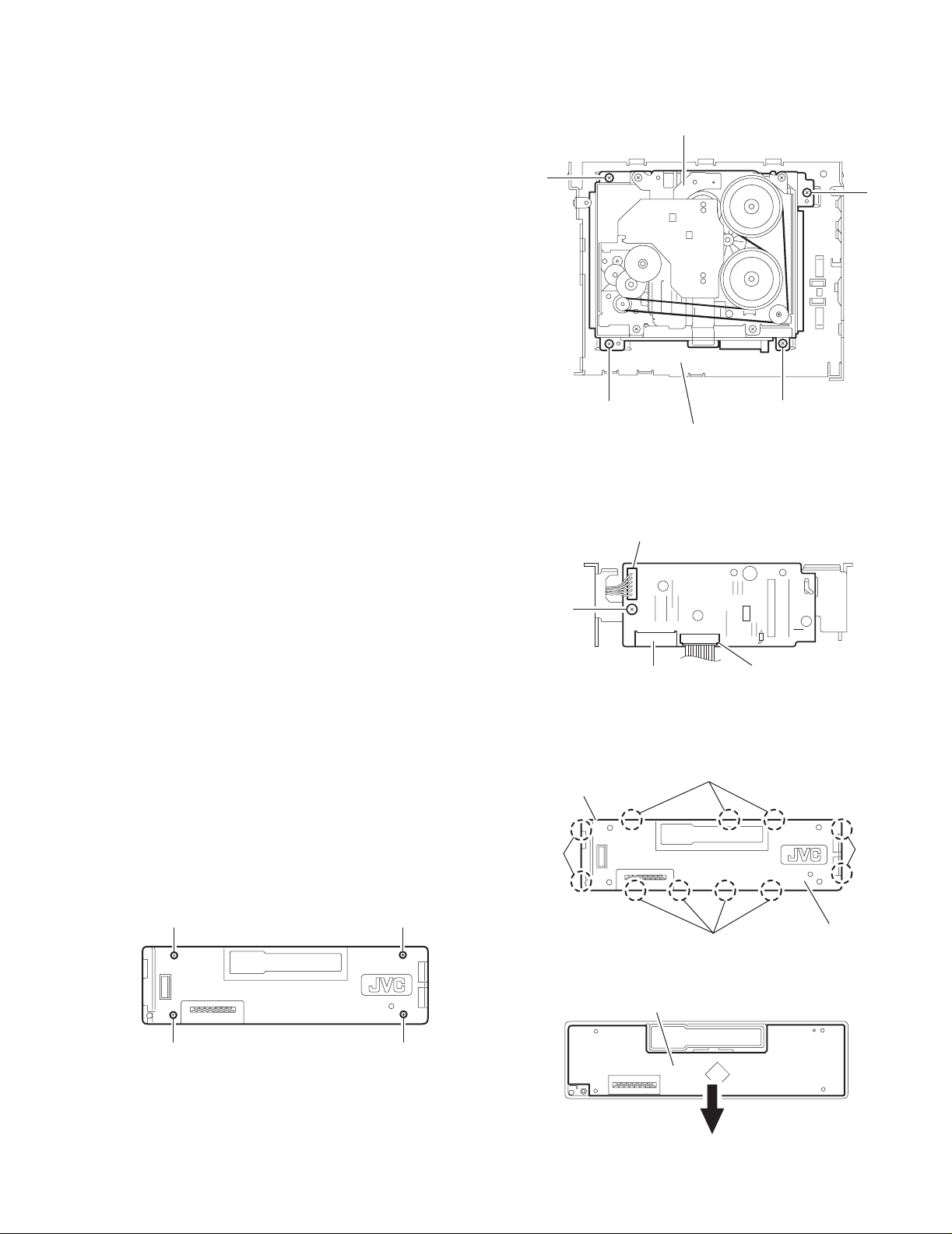
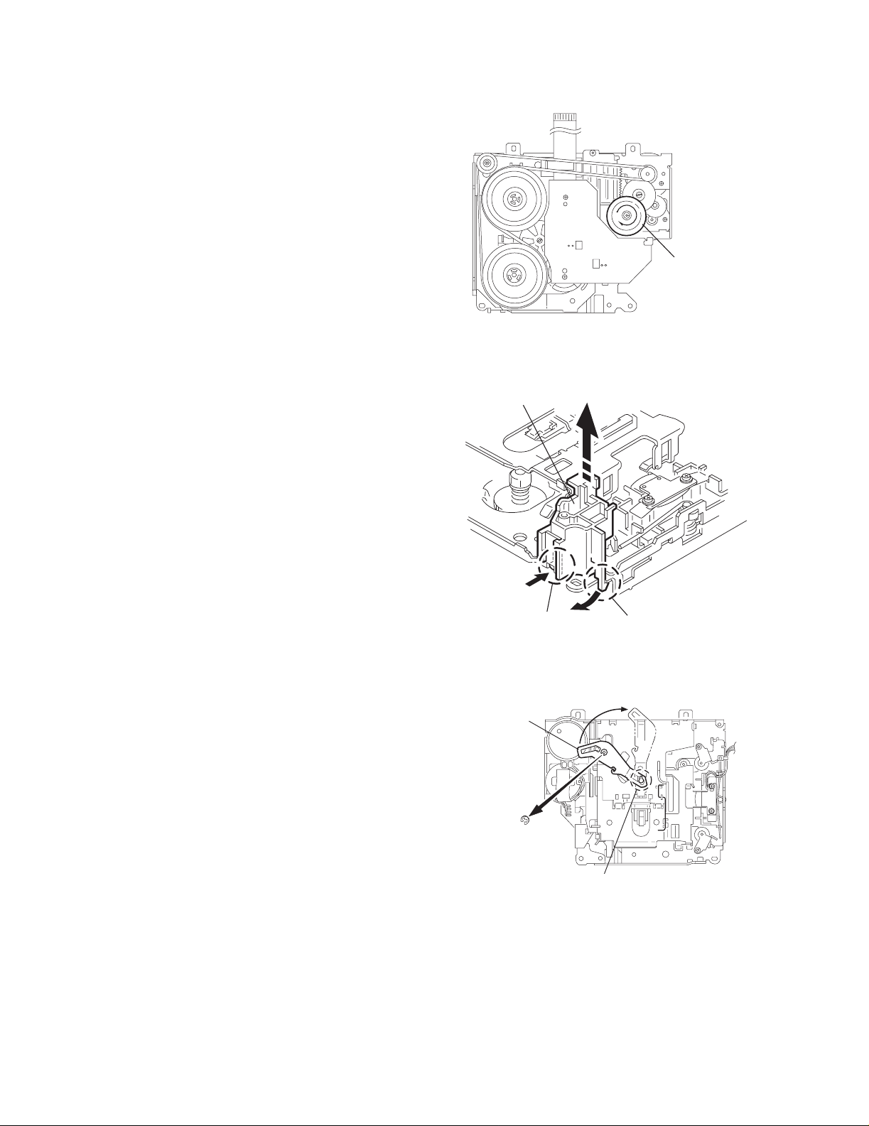
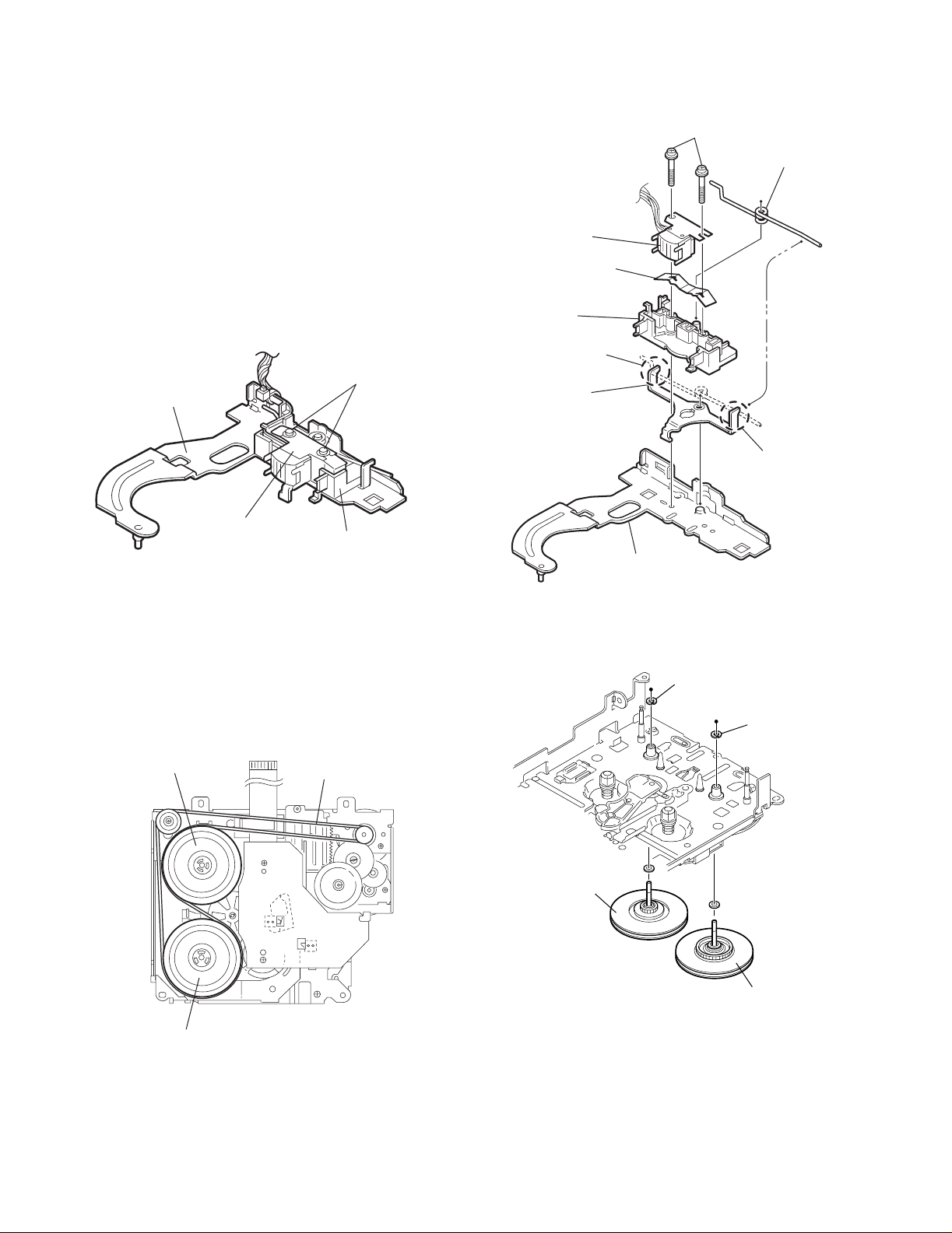
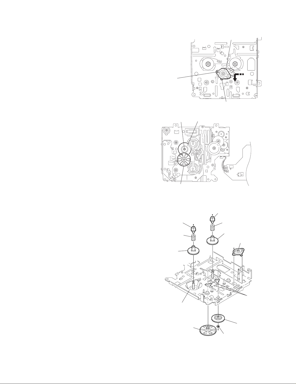
2.1.7 Removing the cassette mechanism assembly
(See Fig.7)
• Prior to performing the following procedure, remove the front
panel assembly, bottom cover, front chassis, heat sink, rear
panel and main board.
(1) Remove the four screws H attaching the cassette mecha-
nism assembly from the top chassis.
2.1.8 Removing the mecha bo ar d
(See Fig.8)
• Prior to performing the following procedure, remove the front
panel assembly, bottom cover, front chassis, heat sink, rear
panel, main board and cassette mechanism assembly.
(1) Disconnect the wire from the connectors CN402 and
CN403 on the mecha board.
(2) Remove the screw J attaching the mecha board.
KS-FX621
Cassette mechanism assembly
H
H
H H
Top chassis
Fig.7
CN402
J
2.1.9 Removing the front board
(See Figs.9 to 11)
• Prior to performing the following procedure, remove the front
panel assembly.
(1) Remove the four screws L attaching the rear cover on the
back of the front panel assembly. (See fig.9)
(2) Release the eleven joints f, the front panel and the rear
cover become separate. (See fig.10)
(3) Remove the front board from the front panel assembly.
(See fig.11)
K
K
K K
Fig.9
CN401
Front panel assembly
Joint h
LCD & Key control board
Fig.8
Joint h
Joint h
Fig.10
CN403
Joint h
Rear cover
Fig.11
(No.49825)1-5
Page 6
KS-FX621
r
2.2 CD Mechanism Assembly
REFERENCE:
Prior to performing the following procedures, turn the mode
gear on the bottom of the body until the respective part comes
to the EJECT position (Refer to Fig.1).
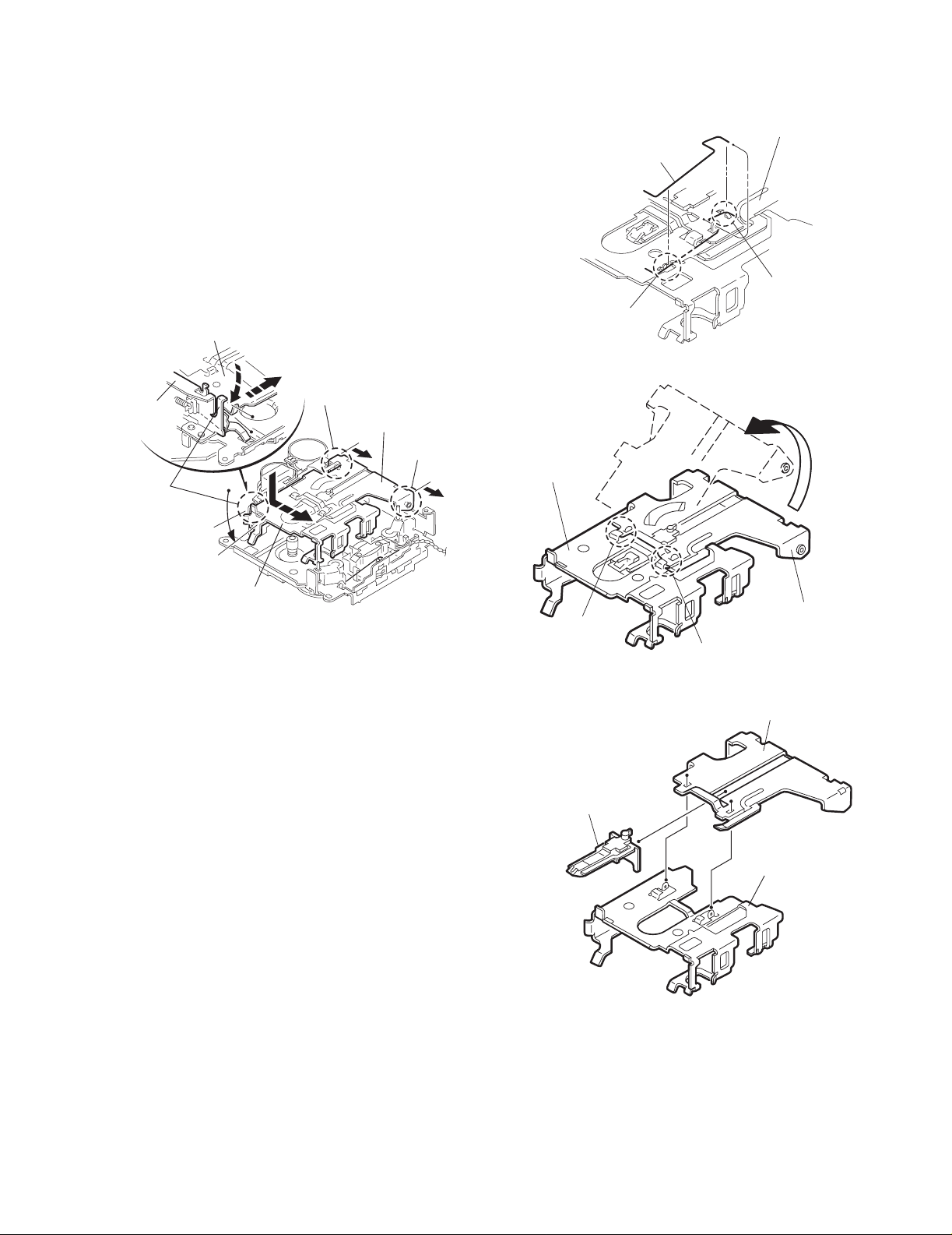
2.2.1 Removing the cassette guide
(See Fig.2)
(1) Turn the mode gear to set to RVS play or subsequent
mode.
(2) Remove the casse tte guide from the main chassis while re-
leasing each two joint tabs a in the direction of the arrow.
Mode gea
Fig.1
Cassette guide
2.2.2 Removing the load arm
(See Fig.3)
(1) Remove the E-washer attaching the load arm.
(2) Move the load arm in the direction of the arrow and release
the joint b on the cassette catch.
Load arm
E-washer
Tab a
Tab a
Fig.2
Joint b
Fig.3
1-6 (No.49825)
Page 7
2.2.3 Removing the cassette hanger assembly / cassette holder
y
(See Fig.4 to 7)
(1) Check the mode is set to EJECT. Push down the front part
of the cassette holder and move in the directi on of the arrow to release the joint c.
(2) Move the rear part of the cassette hanger assembly in the
direction of the arrow to release it from the two joint bosses
d.
(3) Release the holder stabilizer spring from the hooks e and
f, then pull out from the cassette hanger assembly.
(4) Bring up the rear side of the cassette hanger assembly to
release the joint g and h.
(5) Pull out the cassette catch from the cassette hanger as-
sembly.
Cassette holder assembly
KS-FX621
Cassette hanger assembly
Cassette stabilizer spring
Hook f
Hook e
Fig.5
Side bracket
Joints c
Cassette holder assembly
Fig.4
Boss d
Cassette hanger
assembly
Boss d
assette holder
ssembly
Cassette hanger assembl
Hook g
Hook h
Fig.6
Cassette hanger assembly
Cassette catch
Cassette holder assembly
Fig.7
(No.49825)1-7
Page 8
KS-FX621
2.2.4 Removing the side bracket assembly
(See Fig.8 to 10)
(1) Remove the screw A attaching the side bracket assembly.
(2) Detach the front side of the side bracket assembly upward
and pull out forward to release the joint i and j in the rear.
CAUTION:
When reassembling, make sure that the boss k of the main
chassis is set in the notch of the load rack under the side
bracket assembly. Do not reattach the load rack on the boss k.
CAUTION:
After reattaching the side bracket assembly, confirm operation.
Side bracket assembly
Joint i
Side bracket assembly
Joint i
Joint j
Load rack
A
Joint j
Boss k
Fig.9
Side bracket assembly
Fig.8
Boss k
Load rack
1-8 (No.49825)
Fig.10
Page 9
2.2.5 Removing the pinch arm (F) assembly
r
r
(See Fig.11 and 12)
(1) Remove the polywasher and pull out the pinch arm (F) as-
sembly.
(2) Remove the compulsion spring.
KS-FX621
Pinch arm (F) assembly
Polywasher
Compulsion spring
Polywasher
Pinch arm
(R) assembly
2.2.6 Removing the pinch arm (R) assembly
(See Fig.11 and 13)
(1) Remove the polywasher and pull out the pinch arm (R) as-
sembly.
Pinch arm
(R) assembly
Pinch arm
(F) assembly
Fig.11
Polywashe
Polywashe
Fig.12
Joint l
Joint l
Slide chassis
assembly
Fig.14
Fig.13
2.2.7 Removing the slide chassis assembly
(See Fig.14 and 15)
REFERENCE:
It is not necessary to remove the head and the tape guide.
(1) Move the slide chassis assembly in the direction of the ar-
row to release the two joints l and remove from the main
chassis.
(2) Remove the rack link.
CAUTION:
When reassembling, first reattach the rack link, and next fit the
boss m and hook n of the slide chassis assembly to the hole
of the main chassis, and engage the two joints l.
Head
Tape guide
Boss m
Rack link
Hook
n
Fig.15
(No.49825)1-9
Page 10
KS-FX621
2.2.8 Removing the head / tape guide
(See Fig.16 and 17)
REFERENCE:
It is not necessary to remove the slide chassis assembly.
(1) Remove the band attaching the wire to the head.
(2) Remove the two screws B, the head and the head support
spring.
(3) Remove the pinch arm spring from the tape guide.
(4) Remove the tape guide and the pinch spring arm.
CAUTION:
When reattaching the pinch arm spring, set both end of it to the
pinch spring arm ( remarked o).
CAUTION:
When reattaching the head, set the wires into the groove of the
tape guide (Fig.16).
Slide chassis assembly
B
Pinch arm spring
Head
Head support spring
Tape guide
o
B
Pinch spring arm
o
Head
Fig.16
2.2.9 Removing the flywheel assembly (F) & (R)
(See Fig.18 and 19)
REFERENCE:
It is not necessary to remove the slide chassis assembly.
(1) Remove the belt at the bottom.
(2) Remove the two polywashers on the upper side.
(3) Pull out each flywheel assembly downward.
Flywheel assembly (F)
Tape guide
Belt
Slid chassis assembly
Fig.17
Polywasher
Polywasher
Flywheel assembly (F)
Flywheel assembly (R)
1-10 (No.49825)
Flywheel assembly (R)
Fig.19
Fig.18
Page 11
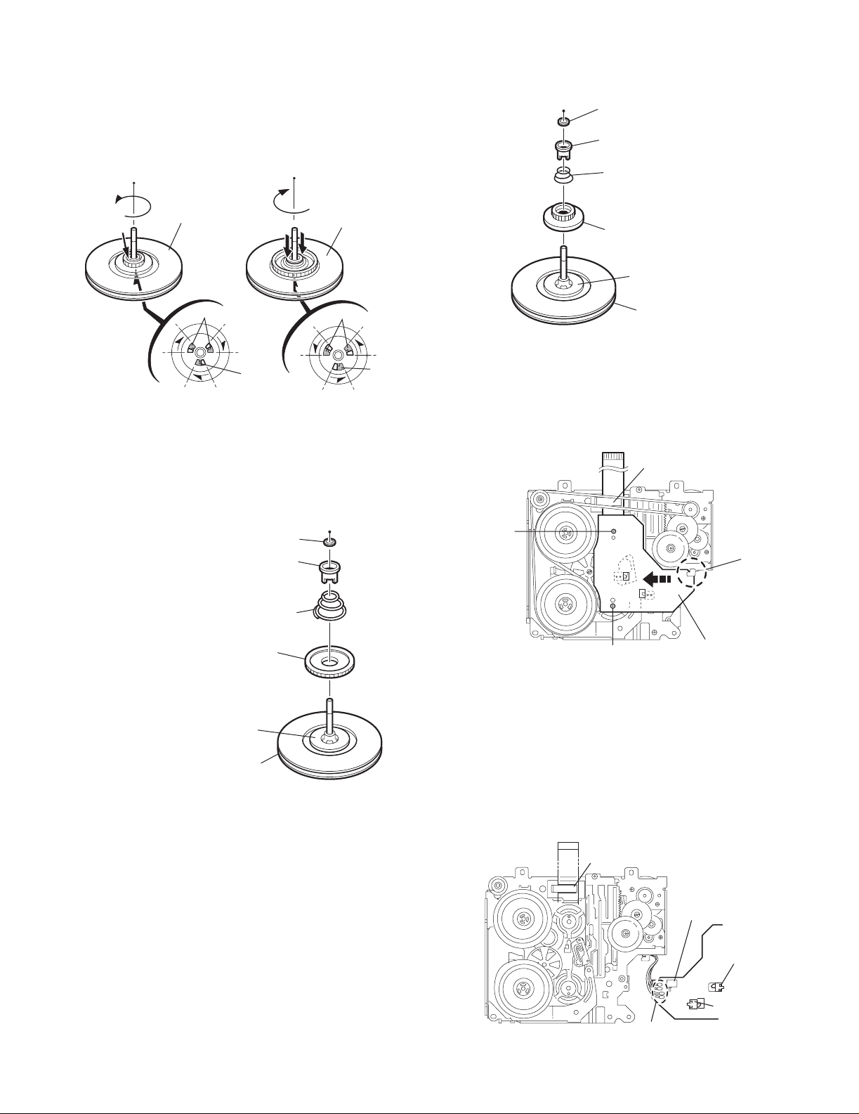
2.2.10 Disassembling the flywheel assembly (F )
r
(See Fig.20 and 21)
(1) Push and turn counterclockwise the spring holder (F) to re-
lease the three joints p on the bottom of the flywheel.
(2) The spring holder (F), the TU spring and the friction gear
play come off.
(3) Remove the polywasher and felt.
KS-FX621
Polywasher
Spring holder (F)
TU spring
Flywheel assembly (F)
Joints p
Joint p
Fig.20
2.2.11 Disassembling the flywheel assembly (R)
(See Fig.20 and 22)
(1) Push and turn clockwise the spring holder (R) to release
the three joints q on the bottom of the flywheel.
(2) The spring holder (R), the FF spring and the friction gear
FF come off.
(3) Remove the polywasher and the felt.
Polywasher
Spring holder (R)
FF spring
Flywheel assembly (R)
Joints q
Joint q
Friction gear play
Felt
Flywheel assembly (F)
Fig.21
FFC pad
C
Joint
Friction gear FF
Felt
Flywheel assembly (R)
Fig.22
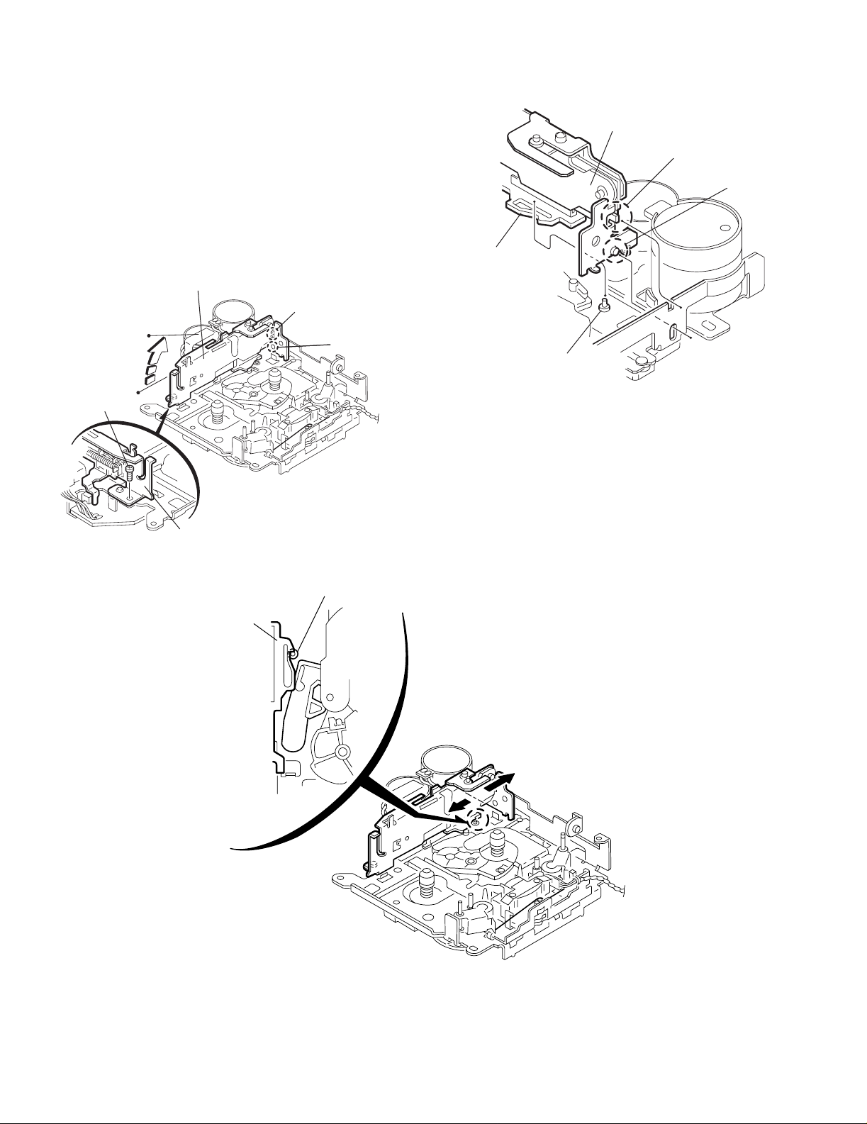
2.2.12 Removing the reel board
(See Fig.23 and 24)
(1) Remove the two screws C attaching the reel board.
(2) Move the reel board in the direction of the arrow to release
the joint r.
(3) Unsolder the wires if necessary.
CAUTION:
When reattaching, confirm operation of the MODE switch and
the ST-BY switch.
The mode position between EJECT and ST-BY is optimum for
reattaching.
Connect the card wire extending from the reel board to the
FFC pad before reattaching the reel board.
C
Reel board
Fig.23
FFC pad
CT-1 switch
MODE switch
ST-BY switch
Soldering
Fig.24
(No.49825)1-11
Page 12
KS-FX621
2.2.13 Removing the gear base arm / gear base link assembly
(See Fig.25 to 27)
(1) Move the gear base arm in the direction of the arrow.
(2) Insert a slotted screwdriver to the gear base spring under
the gear base arm, and release the gear base arm upward
from the boss on the gear base assembly.
(3) Remove the gear base arm from the main chassis while re-
leasing the two joints s.
(4) Move the gear base link assemby in the direction of the ar-
row to release the two joints t.
REFERENCE:
When reattaching the gear base arm, make sure that the boss
on the gear base assembly is inside the gear base spring.
Joint t
Gear base arm
Joints s
Hook u
FFC pad
Hook u
2.2.14 Removing the FFC pad
(See Fig.27 and 29)
(1) Push each joint hook u of the FFC pad and remove toward
the bottom.
Gear base
link assembly
Joint t
Gear base spring
Gear base link assembly
Fig.25
Gear base arm
Screwdriver
Fig.26
Gear base arm
1-12 (No.49825)
FFC pad
Fig.27
Page 13
KS-FX621
r
r
2.2.15 Removing the mode gear
(See Fig.28 and 31)
(1) Remove the polywasher on the bottom and pull out the
mode gear.
2.2.16 Removing the mode switch actuator
(See Fig.28, 29 and 31)
(1) Pull out the mode switch actuator at the bottom.
REFERENCE:
When reattaching the mode switch actuator to the main chassis, make sure to set on the shaft and insert v into the slot w.
2.2.17 Removing the direction link / direction plate
(See Fig.29 to 31)
(1) Remove the polywasher attaching the direction link.
(2) Bring up the direction link to release the three joints x, y
and z at a time.
(3) Move the direction plate in the direction of the arrow to re-
lease the two joints a'.
REFERENCE:
When reattaching the direction plate, engage the two joints a'
and move in the direction of the arrow (Refer to Fig.30).
REFERENCE:
When reattaching the direction link, move the direction plate in
the direction of the arrow and engage the three join t x, y and
z at a time (Refer to Fig.31).
2.2.18 Removing the mode rack assembly
(See Fig.29 and 30)
(1) Move the mode rack assembly in the direction of the arrow
to release the two joints b' and the joint c'.
REFERENCE:
When reattaching, set the two b' Eon the bottom of the mode
rack assembly into the slots of the main chassis and move in
the direction of the arrow (See Fig.30).
Mode switch actuator
Direction plate
Direction plate
Direction link
Fig.28
Slot w
Mode rack assembly
Joints a'
Joint z
Direction link
Polywasher
Joint y
Fig.29
Joint x
Direction plate Mode rack assembly
Joint b'
Mode gear
Polywashe
Joint b'
Joint c'
Joints a'
Fig.30
Direction link
Mode switch actuator
Polywasher
v
Mode gea
Direction plate
Mode rack assembly
Fig.31
(No.49825)1-13
Page 14
KS-FX621
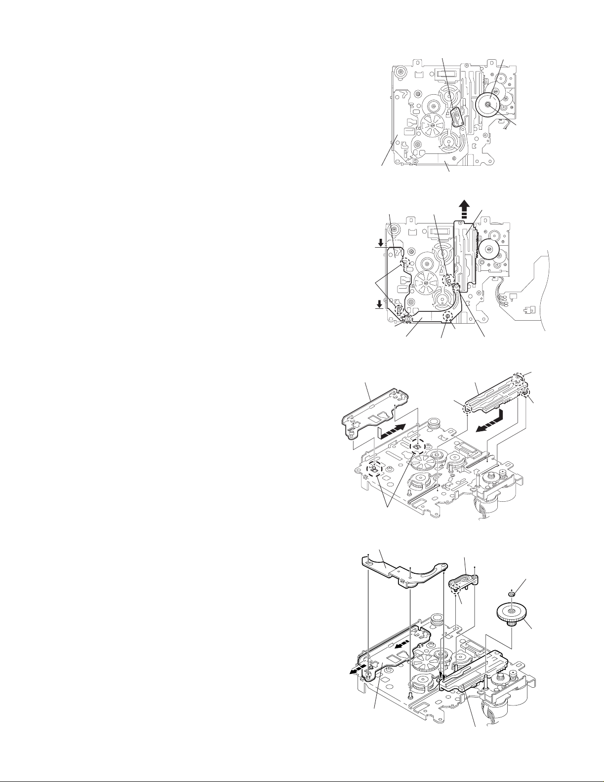
2.2.19 Removing the gear base assembly / take up gear / reflector gear
(See Fig.32 to 34)
(1) Push in the pin d' of the gear base assembly on the upper
side of the body and move the reflector gear toward the
bottom, then pull out.
(2) Remove the polywasher on the bottom and pull out the
take up gear.
(3) Move the gear base assembly in the direction of the arrow
to release it from the two slots e' of the main chassis.
REFERENCE:
The parts are damaged when removed. Please replace with
new ones.
Slot e'
Gear base assembly
Pin d'
Slot e'
Fig.32
2.2.20 Removing the reel driver / reel spindle
(See Fig.34)
(1) Draw out the reel driver from the shaft on the main chassis
and remove the reel driver spring and the reel spindle respectively.
CAUTION:
The reel driver is damaged when removed. Please replace
with a new one.
Polywasher
Reflector gear
Reel driver
Reel driver spring
Reel spindle
Take up gear
Fig.33
Reel driver
Reel driver spring
Reel spindle
Gear base assembly
1-14 (No.49825)
Main chassis
Reflector gear
Slots e
Take up gear
Polywasher
Fig.34
Page 15
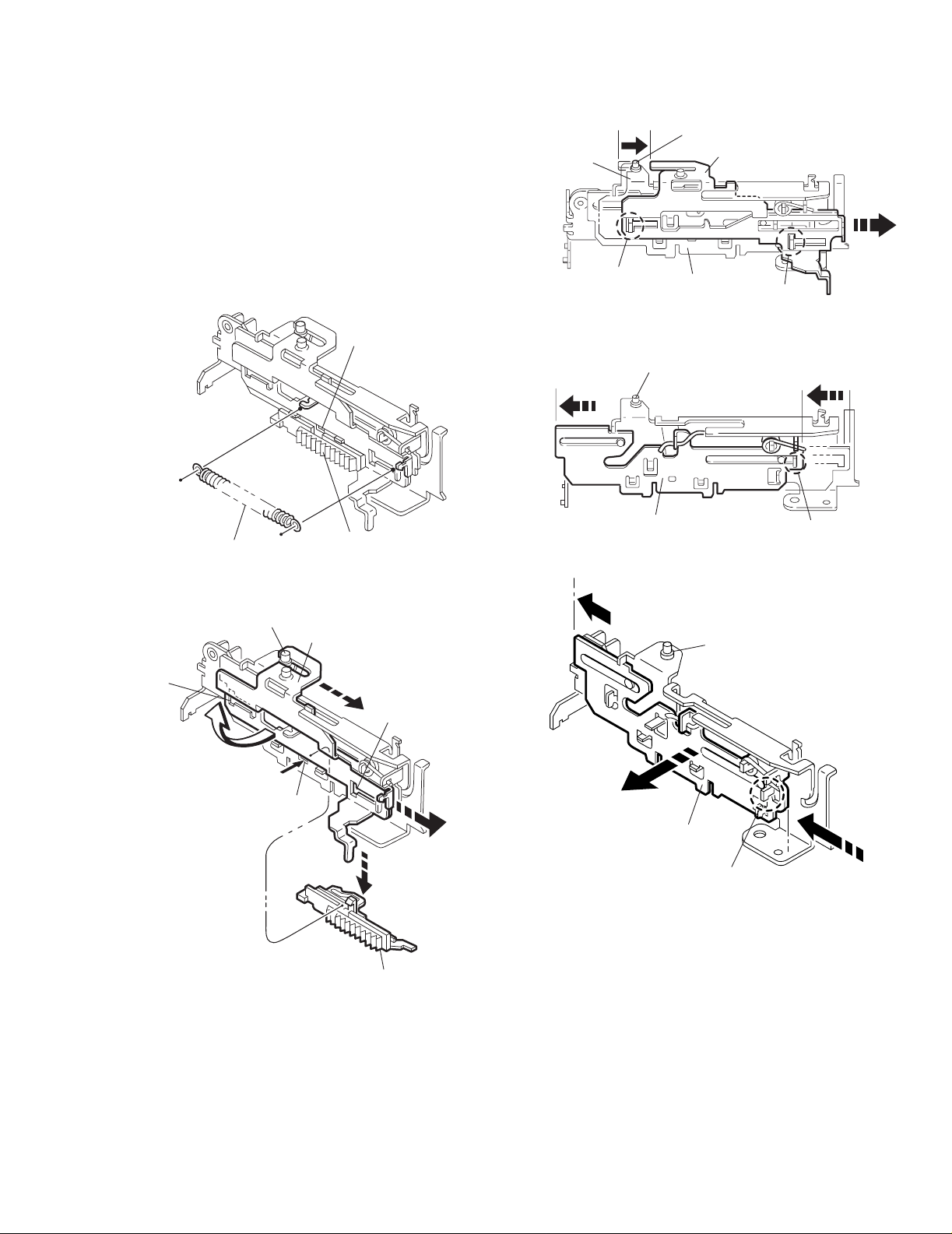
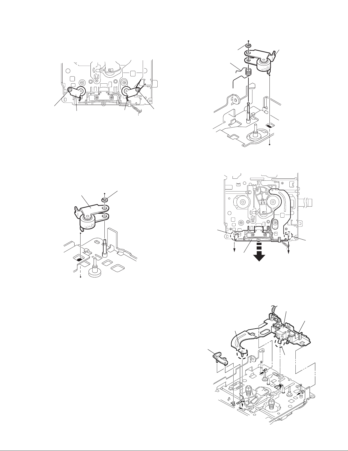
2.2.21 Removing the side bracket assembl y
(See Fig.35 to 39)
(1) Remove the eject cam plate spring.
(2) Push the joint f' through the slot to remove the load rack
downward.
(3) Move the eject cam limiter in the direction of the arrow to
release it from the boss g'of the side brack et assembly and
from the two joints h'.
(4) Move the eject cam plate in the direction of the arrow to re-
lease the joint i'.
CAUTION:
When reassembling, confirm operation of each part before reattaching the eject cam plate spring.
Joint f'
Side bracket
assembly
Boss g'
Eject cam limiter
Joint h'
Eject cam plate
Fig.37
Side bracket assembly
Boss g'
KS-FX621
Joint h'
Eject cam plate spring
Side bracket assembly
Boss g'
Joint h'
Fig.35
Eject cam limiter
Joint f'
Load rack
Joint h'
Eject cam plate
Eject cam plate
Joint i'
Fig.38
Side bracket assembly
Joint i’
Fig.39
Fig.36
Load rack
(No.49825)1-15
Page 16
KS-FX621
r
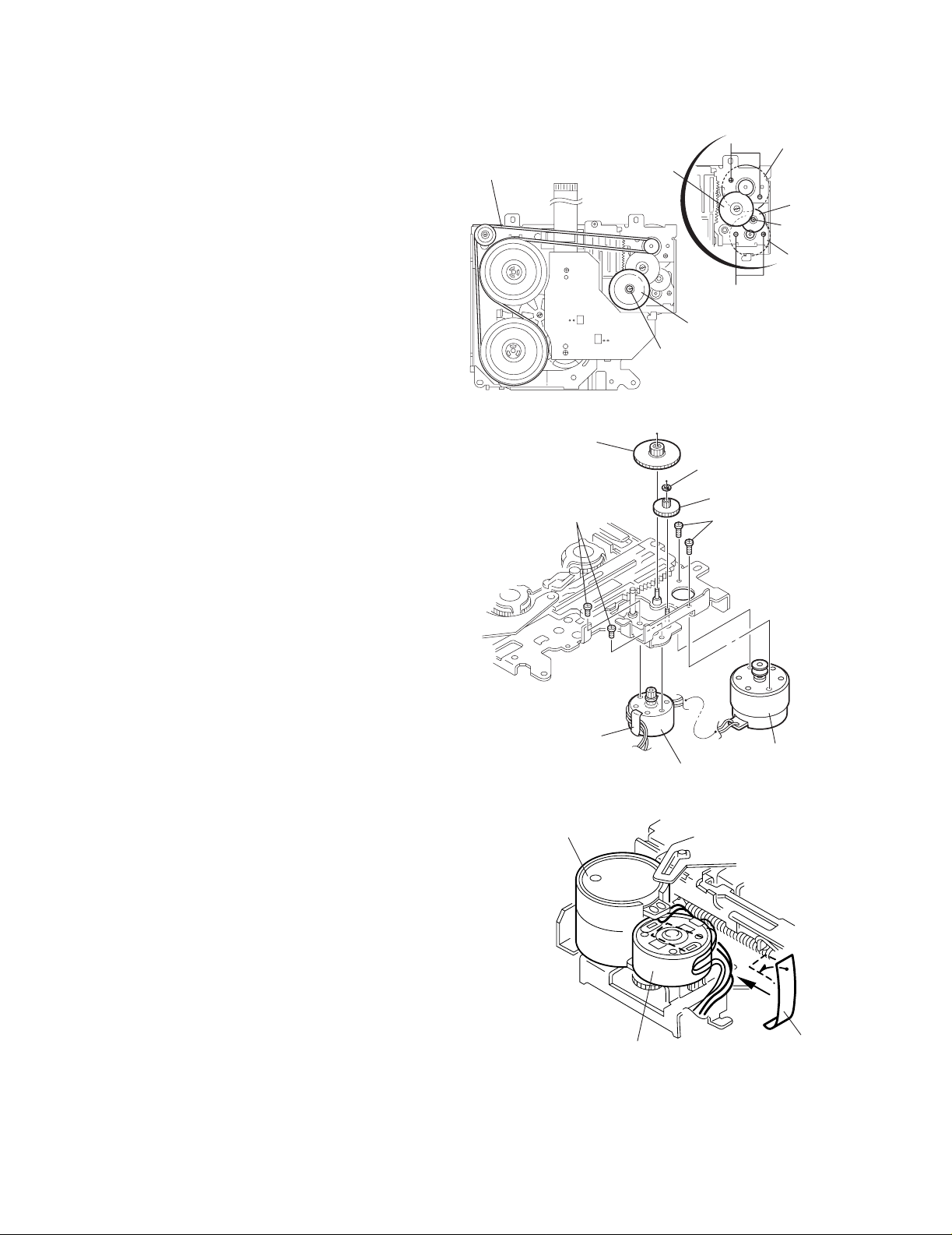
2.2.22 Removing the main motor assembly / sub motor assembly
(See Fig.40 to 42)
(1) Remove the belt at the bottom.
(2) Remove the polywasher and pull out the mode gear.
(3) Pull out the reduction gear (B).
(4) Remove the polywasher and pull out the reduction gear
(A).
(5) Remove the two screws D attaching the main motor as-
sembly.
(6) Remove the two scre ws E attaching the sub motor assem-
bly.
(7) Unsolder the wires on the reel board if necessary.
CAUTION:
When reassembling, adjust the length of the wires extending
from the sub motor asswmbly by attaching them to the side of
the sub motor assembly with the wires extending from the
main motor assembly using a spacer.
Belt
Reduction gear (B)
Reduction gear (B)
Mode gear
Polywasher
Fig.40
Polywasher
D
E
Main motor
assembly
Reduction
gear (A)
Polywashe
Sub motor
assembly
E
Spacer
Main motor assembly
Reduction gear (A)
D
Main motor assembly
Sub motor assembly
Fig.41
1-16 (No.49825)
Sub motor assembly
Fig.42
Spacer
Page 17
SECTION 3
Adjustment
3.1 Adjustment method
Test instruments reqired for adjustment Standard volume position
1. Digital oscilloscoe(100MHz)
2.Frequency counter meter
3.Electric voltmeter
4.Wow & flutter meter
5.Test tapes
VT724.......................for DOLBY level measurement
VT739............For playback frequency measurement
VT712....For wow flutter & tape speed measurement
VT703.....................For head azimuth measurement
6.Torque gauge...................Cassette type for CTG-N
(Mechanism adjustment)
Measuring conditions(Amplifier section)
Balance and Bass, Treble volume, Fader
: Center(Indication"0")
Loudness, Dolby NR, Sound, Cruise : Off
Volume position is about 2V at speaker output with
following conditions, Playback the test tape VT721.
AM mode 999kHz/62dB, INT/400Hz, 30%
modulation signal on recieving.
FM mono mode 97.9MHz/66dB, INT/400Hz, 22.5kHz
deviation pilot off mono
FM stereo mode 1kHz, 67.5kHz dev.pilot 7.5kHz dev
Output level 0dB (1 V,50 /open terminal)
KS-FX621
Power supply voltage.............. DC14.4V(11V to 16V allowance)
Load impedance............ 4 (4 to 8 allowance)
Line out level/Impedance..............1.0V/20k load (250 nWb/m)
Frequency band
Band
FM
AM
87.5 MHz to 108.0MHz
522 kHz to 1620 kHz
MW
LW
144 kHz to 279 kHz
(No.49825)1-17
Page 18

KS-FX621
Information for using a car audio service jig
1. We're advancing efforts to make our extension cords common for all car audio products.
Please use this type of extension cord as follows.
2. As a U-shape type top cover is employed, this type of extension cord is needed to check operation of the
mechanism assembly after disassembly.
3. Extension cord : EXTKSRT002-18P ( 18 pin extension cord ) For connection between mechanism assembly
and main board.
4. Check for mechanism driving section such as motor ,etc.
D
i
sassembl
1. Remove the front panel assembly.
2. Remove the bottom cover.
3. Remove the front chassis.
4. Remove the rear panel.
5. Remove the heat sink.
6. Remove the main board.
7. Reattach the heat sink with two screw B. (Refer to Disassembly method.)
8. Install the front chassis and front panel assmbly.
9. Confirm that current is being carried by connecting an extension cord jig.
Note
Available to connect to the CJ701 connector when installing the front panel.
y met
hod
CAUTION :
Be sure to attach a heat sink on the power amplifier IC of a main board when supplying the power.
If voltage is applied without attaching the heat sink, the power amplifier IC will be destroyed by heat.
To
Cassette mechanism
Extension cord
EXTKSRT002-18P
To
Main board
EXTKSRT002-18P
Cassette mechanism
1-18 (No.49825)
Front panel assembly
Main board
Page 19

Arrangement of adjusting & test points
A
Cassette mechanism
(Surface)
Motor assembly
Tape speed adjust
KS-FX621
Azimuth screw
(Forward)
Playback head
Head section view
Azimuth screw B
(Reverse)
Azimuth screw B
(Reverse)
Playback head
Azimuth screw A
(Forward)
(No.49825)1-19
Page 20

KS-FX621
Item
Head
1.
azimuth
adjustment
Conditions
Test tape:
SCC-1659
VT703(10kHz)
Adjustment and Confirmation methods
Head height adjustment
Adjust the azimuth directly. When you
adjust the height using a mirror tape,
remove the cassette housing from the
mechanism chassis. After installing the
cassette housing, perform the azimuth
adjustment.
Load the SCC-1659 mirror tape. Adjust with
1.
height adjustment screw A and azimuth
adjustment screw B so that line A of the
mirror tape runs in the center between Lch
and Rch in the reverse play mode.
After switching from REV to FWD then to
2.
REV, check that the head position set in
procedure 1 is not changed. (If the position
has shifted, adjust again and check.)
Adjust with azimuth adjustment screw B so
3.
that line B of the mirror tape runs in the
center between Lch and Rch in the forward
play mode.
Head azimuth adjustment
Load VT724 (1kHz) and play it back in
1.
the reverse play mode.
Set the Rch output level to max.
Load VT703 (10kHz) and play it back in
2.
the forward play mode. Adjust the Rch
and Lch output levels to max, with
azimuth adjustment screw B. In this case,
the phase difference should be within 45 .
Engage the reverse mode and adjust the
3.
output level to max, with azimuth
adjustment screw C.
(The phase difference should be 45 or
more.)
When switching between forward and
4.
reverse modes, the difference between
channels should be within 3dB. (Between
FWD L and R, REV L and R.)
S.Values Adjust
A line
Head shield
The head is at low position
during.
B line
Head shield
The head is at High position
during REV.
Output
level:
Maximum
PBHead
FWD Adj B
REV Adj C
(0 ) (45 )
HEIGHT Adj A
phase
Tape speed
2.
and wow
flutter
confirmation
Play back
3.
frequency
response
confiramation
1-20 (No.49825)
When VT721 (315Hz) is played back,
5.
the level difference between channels
should be within 1.5dB.
Test tape: VT712
(3kHz)
Test tape: VT724
(1kHz)
VT739
(63Hz / 1kHz / 10kHz)
The tuner section is of an adjustment-freedesign. In case the tuner is in trouble, replace the tuner pack.
Check to see if the reading of the F, counter /
1.
wow flutter meter is within 3015Hz to 3045Hz
(FWD/ REV), and less than 0.35% (JIS RMS).
In case of out of specification, adjust the
2.
motor with a built-in volume resistor.
Play test tape VT724, and set the volume
1.
position at 2V.
Play test tape VT739 and confirm.
2.
1kHz / 10kHz: -1 3dB,
1kHz / 63Hz: 0 3dB,
When 10kHz is out of specification, it will be
3.
necessary to read adjust the azimuth.
Tape speed:
3015Hz
to 3045Hz
Wow
flutter: less
than 0.35%
Speaker out
1kHz / 63Hz
: 0 3db
1kHz / 10kHz
: -1 3db
Built-in volume
resistor
Page 21

4.1 CXA2559Q (IC401) : Head amp.
•Pin layout
KS-FX621
SECTION 4
Description of major ICs
• Block diagram
1
10
31
32
33
34
35
36
37
38
39
40
45k
30
7k/12k
300k
300k
7k/12k
30
21
F2
30k
30k
F1
29
-
+
+
-
28
100k
X1
X1
100k
27
T2
T1
26
TAPE EQ
FWD/RVS
LPF
25
BIAS
MUTE
Vcc
+
-
F3
+
+
24
-
-
23
24dB
24dB
22
MS MODE
MS ON/
OFF
DET
21
20
19
18
17
16
15
14
13
12
11
1
2
3
4
5
6
7
8
9
10
(No.49825)1-21
Page 22

KS-FX621
c
Y
Y
Y
Y
4.2 HD74HC126P (IC801) : Changer control
• Pin arrangement • Pin function
11C
21A
31Y
14
13
12
Vc
4C
4A
Input Output
CA Y
LX Z
HL L
HH H
• Block diagram
42C
52A
62Y
7GND
11
10
4Y
3C
9
3A
8
3Y
( TOP VIEW )
1A
1
1C
2A
2
2C
3A
3C
4A
4C
3
4
1-22 (No.49825)
Page 23

4.3 KIA7810PI (IC902) : Regulator
•Pin layout
1 2 3
• Block diagram
KS-FX621
1 INPUT
R4 R18
Q12
R5
Z1
R6
R7
R1
Q1
Q13
R10 R3
Q8
Q10
Q5
Q7
R8
R2
Q6
Q2
R15
Q14
C1
R14
Q4
Q9
R16
R9
Q15
Q3
Q11
R13
R21
R17
Q16
R12
R19
Q17
R11
3 OUTPUT
R20
2 GND
(No.49825)1-23
Page 24

KS-FX621
4.4 LC72366-9B41 (IC701) : Micon
• Pin layout
65 ~ 80
64 ~ 41
40 ~ 25
1 ~ 24
• Pin function
Pin No. Symbol I/O Function
1 XIN I 4.5MHz crystal oscillation
2 TEST2 - Connect to ground
3 J-BUS SI I J-BUS signal data input (to 74HC126)
4 J-BUS SO O J-BUS signal data output (to 74HC126)
5 J-BUS SCK O J-BUS output clock signal (to 74HC126)
6 J-BUS I/O I/O J-BUS I/O control ie. "H" = "O", "L" = "I" (to 74HC126)
7NC-No use
8 LCD SO O LCD driver data output (to LC75823E pin 64)
9 LCD SCK O LCD driver clock signal (to LC75823E pin 63)
10 LCD CE O LCD driver chip enable port (to LC75823E pin 62)
11 NC - No use
12 SDA O E. volume data output (to TEA632 0T pin 1)
13 SCL O E. volume clock output (to TEA6320T pin 32)
14 NC - No use
15 TUNER_ILL O Connect to LED (of TUNER button )
16 TAPE_ILL O Connect to LED (of TAPE button)
17 CD_ILL O Connect to LED (of CD button)
18 DIMMER O Connect to display lamp supply
19~24 NC - No use
25 KS1 O Output for initial setting diode matrix
26 KS0 O Output for initial setting diode matrix
27 K3 I Input for initial setting diode matrix
28 K2 I Input for initial setting diode matrix
29 K1 I Input for initial setting diode matrix
30 K0 I Input for initial setting diode matrix
31 Vdd - 5V supply
32 TEST I Change key input to test mode
33 FF/REW O Change MS IC input sensitivity (L at FF/REW)
34 SEEK/STOP O IF count REQ and output [H] at seek.and scan
35 MONO O Output [H] at FM forced monoral mode
36 R/T O Output of mode radio / tape (Radio:H.Tape:L)
37 NC - No use
38 POWER ON - Output [H] at power on
39 ACC O Output [H] during [ACC DET] is [H]
40 IFC CONT O IF count control output (To tuner cct)
41 MOTER O Main motor output (Drive:H Stop:L)
42 SUB MOTER+ O Sub motor output (sub motor loading )
43 SUB MOTER- O Sub motor output (sub motor eject)
44 BEEP O Beep on (output f :2.25KHz)
1-24 (No.49825)
Page 25

Pin No. Symbol I/O Function
45 TAPE IN I Detect cassette in SW. [H] at cassette in
46 STAND BY I Detect stand by SW position.
47 REEL I Pulse input
48 MODE I Detect mode position.
49 F/R O Output F/R ( Forward:L Reverse:H)
50 MS IN I Detect MS. [H] at no music.
51 SD/ST I Station detect and FM stereo signal input [H] at SD
52 DETACH I Front panel detect
53 JOG-0 I Rotary encoder input 0
54 JOG-1 I Rotary encoder input 1
55 JBUS INT I J-BUS interrupt (to 74HC126)
56 REMOCON I Remocon input
57 BAND O FM/AM band selection ("H" : FM, "L" : AM)
58 DOLBY O Output DOLBY mode ("H" : DOLBY on)
59 IFRQ/AGC O During FM auto search IF request output 'H' after SD detected.
During AM auto search AGC output ("H" : auto search)
60 MUTE O Muting switch
61 P.SAVE2 I Power save 2 : +B detect
62 LEVEL I Level meter input
63 S.METER I S meter input
64 KEY2 I Key 2 data input (AD)
65 KEY1 I Key 1 data input (AD)
66 KEY0 I Key 0 data input (AD)
67 P.SAVE1 I Power save 1, ACC power detect
68 SNS I Voltage sense
69 NC 70 FM IF COUNT I FM IF counter data input
71 NC 72 NC 73 Vdd - 5V supply
74 NC 75 FM OSC I FM input frequency
76 Vss - Ground
77 NC 78 EO O PLL error output signa l
79 TEST1 - Connect to ground
80 XOUT O 4.5MHz crystal oscillation
KS-FX621
(No.49825)1-25
Page 26

KS-FX621
4.5 LA4743K (IC301) : Power amp.
• Block diagram
IN 1
TAB
IN 2
+
0.22 F
+
0.22 F
11
1
12
Vcc 1/2 Vcc 3/4
6 20
-
+
Protective
circuit
-
+
2200 F 0.022 F
+
9
-
7
+
OUT 1+
OUT 1-
PWR GND1
8
+
OUT 2+
5
-
OUT 2-
3
PWR GND2
2
ST BY
R.F
47 F
IN 3
PRE GND
IN 4
+5V
ST ON
+
0.22 F
N.C
+
0.22 F
4
Stand by
Switch
Mute
10
+
Ripple
Filter
Mute
22
circuit
3.3 F
+
15
-
+
-
17
19
10K
+
OUT 3+
OUT 3-
Low Level
Mute ON
25
18
21
23
PWR GND3
OUT 4+
OUT 4-
13
14
Protective
circuit
-
+
+
-
ON TIME C
1-26 (No.49825)
22 F
Muting &
16
+
ON Time Control
Circuit
PWR GND4
24
Page 27

4.6 PT6523LQ (IC651) : LCD driver
•Pin layout
48 ~ 33
49
KS-FX621
32
• Block diagram
64
1 ~ 16
17
COMMON
DRIVER
CLOCK
GENERATOR
ADDRESS
DETECTOR
SEGMENT DRIVER & LATCH
SHIFT REGISTER
• Piin function
Pin No. Pin Name I/O Description
1~ 52 SG1 ~ SG52 O Segment Output Pins
53~55 COM1 ~ COM3 O Common Driver Output Pins
56 VDD - Power Supply
57 INH
I Display OFF Control Input Pin
When this pin is "Low", the Display is forcibly turned OFF. (SG1 to SG52, COM1 to COM3 are
set to "LOW"). (See Note 1)
When this pin is set to "High", the Displa is ON.
58 VDD1 I Used for the 2/3 Bias Voltage when the Bias Voltages are provied externally. Connect to VDD2
when 1/2 Bias is used.
59 VDD2 I Used for 1/3 Bi as Voltage when the Bias Voltages are provided externally. Connect to VDD1
when 1/2 Bias is used.
60 VSS - Ground Pin.
61 OSC I/O Oscillation Input /Outout Pin
62 CE I Chip Enable Pin
63 CLK I Synchronization Clock
64 DI I Transfer Data Pin
Note 1:
When INH
= "LOW" : Serial data trensfers can be performed when the display is forcibly OFF.
(No.49825)1-27
Page 28

KS-FX621
4.7 RPM6938-SV4 (IC652) : Remote sensor
• Pin diagram
1 2 3
• Block diagram
AGC
AMP
I/V
conversion
PD
magnetic shield
BPF
fo
trimming
circuit
Detector
4.8 LB1641 (IC402) : DC motor driver
• Pin layout • Truth table
GND
OUT1
P1
VZ
IN1
IN2
VCC1
VCC2
P2
OUT2
1
2
3
4
5
6
7
8
9
10
Input Output Mode
IN1 IN2 OUT1 OUT2
0000 Brake
1010 CLOCKWISE
0 1 0 1 COUNTER-CLOCKWISE
1100 Brake
Vcc
Comp
Vcc
22k
Rout
GND
1-28 (No.49825)
Page 29

4.9 TEA6320T-X (IC161) : E.volume
•Pin layout
SDA
1
GND
TL
B2L
B1L
IVL
ILL
QSL
IDL
MUTE
ICL
IMD
IBL
IAL
2
3
4
5
6
7
8
9
10
11
12
13
14
15
16
CD-CH
TAPE
TUNER
OUTLR
OUTLF
• Block diagram
10 8 9 7 6
32
31
30
29
28
27
26
25
24
23
22
21
20
19
18
17
SCL
VCC
OUTRR
OUTRF
TR
B2R
B1R
IVR
ILR
QSR
IDR
Vref
ICR
CAP
IBR
IAR
KS-FX621
5
12
21
31
2
19
POWER
SUPPLY
VOLUME 1
+20 to -31 dB
LOUDNESS
LEFT
16
15
13
11
14
22
20
SOURCE
SELECTOR
VOLUME 1
+20 to -31 dB
LOUDNESS
RIGHT
18
17
23 25 24 26 27 28
• Pin functions
Pin No. Symbol I/O Functions
1 SDA I/O Serial data input/output.
2 GND - Ground.
3 OUTLR O output left rear.
4 OUTLF O output left front.
5 TL I Treble control capacitor left channel or
input from an external equalizer.
6 B2L - Bass control capacitor left channel or
output to an external equalizer.
7 B1L - Bass control capacitor left channel.
8 IVL I Input volume 1. left control part.
9 ILL I Input loudness. left control part.
10 QSL O Output source selector. left channel.
11 IDL - Not used
12 MUTE - Not used
13 ICL I Input C left source.
14 IMO - Not used
15 IBL I Input B left source.
16 IAL I Input A left source.
BASS
LEFT
+15 dB
LOGIC
BASS
RIGHT
+15 dB
VOLUME 2
0 to 55 dB
BALANCE
FENDER REAR
VOLUME 2
0 to 55 dB
BALANCE
FENDER FRONT
HC BUS
REC
3
4
32
TREBLE
LEFT
+12 dB
MUTE
FUNCTION
ZERO CROSS
DETECTOR
1
VOLUME 2
TREBLE
RIGHT
+12 dB
0 to -55dB
BALANCE
FENDER FRONT
VOLUME 2
0 to -55dB
BALANCE
FENDER REAR
29
30
Pin No. Symbol I/O Functions
17 IAR I Input A right source.
18 IBR I Input B right source.
19 CAP - Electronic filtering for supply.
20 ICR I Input C right source.
21 Vre f - Reference voltage (0.5Vcc)
22 IDR - Not used
23 QSR O Output source selector right channel.
24 ILR I Input loudness right channel.
25 IVR I Input volume 1. right control part.
26 B1R - Bass control capacitor right channel
27 B2R O Bass control capacitor right channel or
output to an external equalizer.
28 TR I Treble control capacitor right channel or
input from an external equalizer.
29 OUTRF O Output right front.
30 OUTRR O Output right rear.
31 Vcc - Supply voltage.
32 SCL I Serial clock input.
(No.49825)1-29
Page 30

KS-FX621
4.10 AN80T05 (IC901) : Regulator
• Terminal layout & Block diagram
Reference Voltage
Thermal
Protection
ASO & Peak
Current Protection
Pre
Drive
Pre
Drive
AMP
Out
AMP
Out
Pre
Drive
123456789101112
ILL
10V
MODE2 MODE1 STB VDD
5.6V
AMP VCC ANT COM
• Pin function
Pin No. Symbol Function
1 ILL 10V power supply for illumination.
2 MODE2 When 5V is input,becomes AM. and the antenna output is turned on.
3 MODE1 When 5V is input,becomes AM. and the output of FM is switched.
4 STB When 5V is input outputs to ILL,COM,and AMP. It is 0V usually.
5 VDD 5.6V power supply.
6 AMP Power supply supply to remote amplifier
7 VCC Back up. conn ects with ACC with it.
8 ANT Psower supply supply to auto antenna.
9 COM 8.7V power supply.
10 AM The power supply of 8.7V to AM.
11 FM The power supply of 8.7V to FM.
12 GND Ground
Pre
Drive
8.7VAM8.7VFM8.7V
Pre
Drive
GND
1-30 (No.49825)
Page 31

KS-FX621
(No.49825)1-31
Page 32

KS-FX621
VICTOR COMPANY OF JAPAN, LIMITED
AV & MULTIMEDIA COMPANY MOBILE ENTERTAINMENT CATEGORY 10-1,1chome,Ohwatari-machi,Maebashi-city,371-8543,Japan
(No.49825)
Printed in Japan
200303WPC
Page 33

PARTS LIST
[ KS-FX621 ]
* All printed circuit boards and its assemblies are not available as service parts.
Area suffix
KS-FX621
U --------------------- Other Areas
- Contents -
Exploded view of general assembly and parts list (Block No.M1)
Cassette mechanism assembly and parts list (Block No.MP)
Electrical parts list (Block No.01~03)
Packing materials and accessories parts list (Block No.M3,M5)
3-2
3-4
3-8
3-12
No. 49825 3-1
Page 34

KS-FX621
Exploded view of general assmbly and parts list
56
15
58
59
60
57
15
53
50
54
10
14
17
14
52
A
55
Main board
B
24
25
12
16
20
21
18
16
42
Block No.
41
M
11
M
1
M
48
45
49
47
43
46
LCD1
23
22
19
18
A
8
B
6
9
2
13
5
3
5
42
Front board
5
4
5
7
13
13
1
13
36
38
31
35
51
30
29
28
32
26
27
37
40
34
39
33
44
3-2
Page 35

Exploded view of general
assembly and parts list
Block No. [M][1][M][M]
Symbol No.
1 ------------ MECHA
2 FSYH4036-050 SPACER
3 GE20136-001A MECHA BKT(L)
4 FSKL2002-002 MECHA BKT(R)
5 QYSDST2606Z SCREW 2.6mm x 6mm(x4)
6 QYSDST2606Z SCREW 2.6mm x 6mm
7 LV40847-002A SPACER
8 GE10043-011A TOP CHASIS
9 GE40135-001A EARTH PLATE
10 GE30568-006A HEA T SINK
11 GE30393-001A BOTTOM COVER
12 FSMA3004-203 INSULATOR
13 QYSDST2604Z SCREW 2.6mm x 4mm(x4)
14 FSKZ4005-001 SCREW (x2)
15 QYSDST2604Z SCREW 2.6mm x 4mm(x2)
16 QYSDST2606Z SCREW 2.6mm x 6mm(x2)
17 QYSDST2612Z SCREW 2.6mm x 12mm(x2)
18 QYSDST2004M MINI SCREW 2mm x 4mm(x2)
19 GE10054-001A FRONT CHASSIS
20 GE30583-001A LOCK LEVER
21 FSKW4005-003 TORSION SPRING
22 FSXP3026-002 RLS KNOB
23 FSKW3002-004 COMP. SPRING
24 FSJC3014-003 CASSETTE LID
25 VKW4947-002 DOOR SPRING
26 GE10039-001A FRONT PANEL
27 GE30303-006A FINDER ASSY
28 FSJK3014-001 LIGHT LENS
29 GE20119-001A PRESET BUTTON
30 FSYH4036-077 SHEET
31 GE30304-001A POWER BUTTON
32 GE30305-001A EJECT BUTTON
33 GE20131-012A D.FUNC. BUTTON
34 GE30307-001A SND FUNC BUTTON
35 FSYH4036-032 SHEET
36 GE20130-002A PUSH BUTTON
37 GE20120-001A UP/DOWN BUTTON
38 GE20118-002A +/- BUTTON
39 GE30306-001A DETACH BUTTON
40 FSKW3002-012 COMP.SPRING
41 GE10040-002A REAR COVER
42 VKZ4777-001 MINI SCREW (x4)
43 GE30308-001A LCD LENS
44 GE30309-001A LCD CASE
45 GE30310-001A LENS CASE
46 GE40125-003A LIGHTING SHEET
47 GE40171-001A LIGHTING SHEET
48 GE30648-001A NAME PLATE
49 QNZ0440-001 LCD CONNECTOR
50 QMFZ047-150-T FUSE 15A
51 GE30854-001A LED HOLDER
52 GE30382-013A REAR BRACKET
53 GE40103-002A REG BRACKET
54 GE40136-001A IC BRACKET
55 GE40107-002A HEA T SINK
56 QYSDST2606Z SCREW 2.6mm x 6mm
57 QYSDSF2606Z SCREW 2.6mm x 6mm(x2)
58 QYSDSF2606Z SCREW 2.6mm x 6mm
59 QYSDST2606Z SCREW 2.6mm x 6mm
60 QYSDST2606Z SCREW 2.6mm x 6mm
LCD1 QLD0251-001 LCD MODULE
Part No. Part Name Description Local
KS-FX621
3-3
Page 36

KS-FX621
Cassette mechanism assembly and parts list
59
CDS-802JE3
24
28
64
116
27
108
Block No.
4
M
M
P
M
94
7
33
10
93
17
45
65
11
106
16
44
111
34
117
37
111
43
40
114
46
39
47
66
38
22
50
3
23
63
32
66
96
73
67
91
38
114
25
5
62
35
75
1
114
26
6
51
21
110
31
42
61
49
113
109
109
2
113
41
60
48
3-4
82
87
84
107
83
86
107
85
111
13
74
72
12
71
Page 37

Cassette mechanism
Block No. [M][P][M][M]
Symbol No.
1 X-0802-1009S MAIN CHASSIS AS
2 X-0802-1002S SLIDE CHASSIS A
3 X-0802-1003S SIDE BKT ASSY
4 X-0802-1004S CASSETTE HANGER
5 X-0802-1005S PINCH ARM F ASS
6 X-0802-1006S PINCH ARM R ASS
7 X-0802-1007S GEARBASE LINK A
10 X-0802-2001S MODE RACK ASSY
11 X-0802-2002S GEAR BASE ASSY
12 1-0802-6001S FLYWHEE L ASSY F
13 1-0802-6002S FLYWHEE L ASSY R
16 X-0802-7002S SUB MOTOR ASSY
17 X-0802-7004S MAIN MOTOR ASSY
21 1-0802-1002S DIRECTION PLATE
22 1-0802-1005S DIRECTION LINK
23 1-0802-1006S CASSETTE HOLDER
24 1-0802-1011S EJECT CAM LIMIT
25 1-0802-1012S HEAD SUPT SPG
26 1-0802-1013S PINCH SPG ARM
27 1-0802-1014S LOAD ARM
28 1-0802-1015S EJECT CAM PLA T E
31 1-0101-2056S IDLE PULLEY(A1)
32 1-0802-2001S CASSETTE GUIDE
33 1-0802-2004S GEAR BASE ARM
34 1-0802-2006S LOAD RACK
35 1-0802-2007S TAPE GUIDE
37 1-0802-2009S REDUCTION GEARA
38 1-0802-2010S REEL SPINDLE (x2)
39 1-0802-2011S REEL DRIVER (x2)
40 1-0802-2012S REDUCTION GEARB
41 1-0802-2013S SPG HOLDER F
42 1-0802-2014S SPG HOLDER R
43 1-0802-2015S MODE GEAR
44 1-0802-2016S TAKE UP GE AR
45 1-0802-2017S REFLECTOR GEAR
46 1-0802-2018S RACK LINK
47 1-0802-2019S MODE SW ACTUATR
48 1-0802-2020S FRICTION GEARPL
49 1-0802-2021S FRICTION GEARFF
50 1-0802-2022S CASSETTE CA TCH
51 1-0802-2026S FFC PAD
59 1-0802-4001S EJECT CAM PL SP
60 1-0802-4002S TU SPG
61 1-0802-4003S FF SPG
62 1-0802-4004S PINCH ARM SPG
63 1-0802-4005S HOLDER STA B SPG
64 1-0802-4006S HOLDER CUSH SPG
65 1-0802-4007S GEAR BASE SPG
66 1-0802-4008S REEL DRIVER SPG (x2)
67 1-0802-4013S COMPULSION SPG
71 1-0802-5001S BELT
72 1-0802-5002S FELT 7.5*18.5*1
73 1-0802-5003S AZIMUTH SCREW (x2)
74 1-0802-5004S FELT 11*18.5*1
75 1-0050-5023S WTRE CLAMPER
82 1-0802-7001S REEL PCB DL
83 1-0802-7010S
84 1-0802-7003S SW(MICMPU11750)
85 1-0802-7016S FLAT CABLE 10P
86 1-0801-7024S PHOTO SENSOR
87 1-0802-7009S SW(MICMPU12370)
91 1-0802-7007S
93 1-0801-7009-0S M.MOTOR WIRE B
94 1-0801-7009-1S M.MOTOR WIRE R
96 1-0802-7017S JOINT WIRE ASSY
106 2-1032-0025-C2S SCREW (x2)
107 2-13S2-0025-P2S +PLAIN SCR M2 (x2)
108 2-1112-6035-C2S +PLAIN SCR M2.6
109 2-1816-0032-E8S MYLA R WASHER(S) (x2)
110 2-1812-0032-D2S PSW-S 1.2
111 1-0036-5024S PSW(REEL) (x3)
113 2-1821-0040-D1S POLY W ASH ER (x2)
Part No. Part Name Description Local
SW(MATSUCHITA
ESE22)
HEAD(MITSUMI P-
5344)
Symbol No.
114 2-1821-0040-D2S PSW-S 2.1 (x3)
116 2-1711-5040-16S E RING
117 2-1031-7030-C2S SCREW (x2)
Part No. Part Name Description Local
KS-FX621
3-5
Page 38

KS-FX621
Grease point 1/2
FG-84M
MEA-512R
MEN-223
SW-902
CFD-409
CFD-250H
EP-56
SW-474B
1
2
3
3-6
5
6
4
Page 39

Grease point 2/2
7
KS-FX621
10
21
27
11
24
28
12
13
33
35
41
39
44
46
42
62
3-7
Page 40

KS-FX621
Electrical parts list
Main board
Block No. [0][1][0][0]
Symbol No.
IC161 TEA6320T-X IC
IC301 LA4743K POWER IC
IC701 LC72366-9B41 IC
IC801 HD74HC126P IC
IC901 AN80T05 IC
IC902 KIA7810PI 10V REGULATOR
Q4 KRC102M-T DIGI TRANSISTOR
Q31 KTC3199/GL/-T TR I/M
Q32 KTC3199/GL/-T TR I/M
Q241 KTC3199/GL/-T TR I/M
Q301 KRC102M-T DIGI TRANSISTOR
Q321 2SD2144S/VW/-T TRANSISTOR
Q351 2SD2144S/VW/-T TRANSISTOR
Q701 KTC3199/GL/-T TR I/M
Q781 KRA102M-T DIGI TRANSISTOR
Q782 KRA102M-T DIGI TRANSISTOR
Q901 KTA1267/YG/-T TRANSISTOR
Q902 KRC102M-T DIGI TRANSISTOR
Q903 KRA102M-T DIGI TRANSISTOR
Q904 KRC102M-T DIGI TRANSISTOR
Q905 2SA1855/RST/-T TRANSISTOR
Q906 KRC102M-T DIGI TRANSISTOR
Q907 KTA1267/YG/-T TRANSISTOR
Q976 KTA1267/YG/-T TRANSISTOR
Q977 KTC3199/GL/-T TR I/M
D1 1SS133-T2 SI DIODE
D2 1SS133-T2 SI DIODE
D10 RB721Q-40-T2 DIODE
D31 MTZJ9.1C-T2 Z.DIODE I M
D32 1SS133-T2 SI DIODE
D79 1SS133-T2 SI DIODE
D241 RB721Q-40-T2 DIODE
D242 RB721Q-40-T2 DIODE
D310 1SS133-T2 SI DIODE
D321 1SS133-T2 SI DIODE
D702 1SS133-T2 SI DIODE
D704 1SS133-T2 SI DIODE
D705 MTZJ6.2B-T2 Z DIODE
D706 MTZJ6.2B-T2 Z DIODE
D707 MTZJ6.2B-T2 Z DIODE
D708 MTZJ6.2B-T2 Z DIODE
D709 MTZJ6.2B-T2 Z DIODE
D710 MTZJ6.2B-T2 Z DIODE
D711 MTZJ6.2B-T2 Z DIODE
D715 MTZJ6.2B-T2 Z DIODE
D781 1SS133-T2 SI DIODE
D782 MTZJ11B-T2 Z DIODE
D901 1N5401-F64 DIODE
D902 1SS133-T2 SI DIODE
D903 1A3G-T1 SI DIODE
D904 1A3G-T1 SI DIODE
C1 QERF1CM-106Z E CAPACITOR 10uF 16V M
C2 QEKJ1CM-106Z E CAPACITOR 10uF 16V M
C4 QDVB1EZ-223Y C CAPACITOR 0.022uF 25V Z
C6 QDYB1CM-103Y C CAPACITOR 0.01uF 16V M
C8 QCBB1HK-121Y C CAPACITOR 120pF 50V K
C9 QEKJ1HM-104Z E CAPACITOR 0.1uF 50V M
C10 QDGB1HK-102Y C CA PACITOR 1000pF 50V K
C12 QDYB1CM-103Y C CAPACITOR 0.01uF 16V M
C13 QERF1AM-107Z E CAPACITOR 100uF 10V M
C31 QEKJ1HM-104Z E CAPACITOR 0.1uF 50V M
C32 QEKJ1HM-104Z E CAPACITOR 0.1uF 50V M
C33 QEQF1HM-225Z E CAPACITOR 2.2uF 50V M
C34 QDGB1HK-102Y C CA PACITOR 1000pF 50V K
C35 QERF1AM-227Z E CAPACITOR 220uF 10V M
C81 QDX11EK-183Z C CAPACITOR 0.018uF 25V K
C82 QERF1HM-105Z E CAPACITOR 1uF 50V M
C91 QDX11EK-183Z C CAPACITOR 0.018uF 25V K
C92 QERF1HM-105Z E CAPACITOR 1uF 50V M
Part No. Part Name Description Local
Symbol No.
C162 QERF1HM-105Z E CAPACITOR 1uF 50V M
C163 QERF1HM-105Z E CAPACITOR 1uF 50V M
C164 QFLA1HJ-822Z M CAPACITOR 8200pF 50V J
C165 QFVD1HJ-154Z MF CAPACITOR 0.15uF 50V J
C166 QFVD1HJ-224Z MF CAPACITOR 0.22uF 50V J
C167 QFV61HJ-333Z MF CAPACITOR 0.033uF 50V J
C168 QDXB1CM-562Y C CAPACITOR 5600pF 16V M
C172 QERF1HM-105Z E CAPACITOR 1uF 50V M
C173 QERF1HM-105Z E CAPACITOR 1uF 50V M
C174 QFLA1HJ-822Z M CAPACITOR 8200pF 50V J
C175 QFVD1HJ-154Z MF CAPACITOR 0.15uF 50V J
C176 QFVD1HJ-224Z MF CAPACITOR 0.22uF 50V J
C177 QFV61HJ-333Z MF CAPACITOR 0.033uF 50V J
C178 QDXB1CM-562Y C CAPACITOR 5600pF 16V M
C181 QERF1HM-105Z E CAPACITOR 1uF 50V M
C182 QERF1HM-105Z E CAPACITOR 1uF 50V M
C191 QERF1HM-105Z E CAPACITOR 1uF 50V M
C192 QERF1HM-105Z E CAPACITOR 1uF 50V M
C195 QERF1CM-476Z E CAPACITOR 47uF 16V M
C196 QERF1AM-107Z E CAPACITOR 100uF 10V M
C197 QERF1AM-107Z E CAPACITOR 100uF 10V M
C198 QDYB1CM-103Y C CAPACITOR 0.01uF 16V M
C199 QCFB1HZ-104Y C CAPACITOR 0.1uF 50V Z
C241 QERF1HM-105Z E CAPACITOR 1uF 50V M
C242 QERF1CM-226Z E CAPACITOR 22uF 16V M
C243 QCFB1HZ-473Y C CAPACITOR 0.047uF 50V Z
C244 QERF1HM-474Z E CAPACITOR 0.47uF 50V M
C301 QERF1CM-106Z E CAPACITOR 10uF 16V M
C302 QERF1HM-475Z E CAPACITOR 4.7uF 50V M
C303 QERF1EM-475Z E CAPACITOR 4.7uF 25V M
C304 QCBB1HK-223Y C CAPACITOR 0.022uF 50V K
C305 QERF1CM-226Z E CAPACITOR 22uF 16V M
C306 QCFB1HZ-104Y C CAPACITOR 0.1uF 50V Z
C307 QCFB1HZ-104Y C CAPACITOR 0.1uF 50V Z
C308 QCFB1HZ-104Y C CAPACITOR 0.1uF 50V Z
C309 QCFB1HZ-104Y C CAPACITOR 0.1uF 50V Z
C321 QCBB1HK-471Y C CAPACITOR 470pF 50V K
C322 QFVD1HJ-224Z MF CAPACITOR 0.22uF 50V J
C331 QCBB1HK-471Y C CAPACITOR 470pF 50V K
C332 QFVD1HJ-224Z MF CAPACITOR 0.22uF 50V J
C341 QCBB1HK-471Y C CAPACITOR 470pF 50V K
C342 QFVD1HJ-224Z MF CAPACITOR 0.22uF 50V J
C351 QCBB1HK-471Y C CAPACITOR 470pF 50V K
C352 QFVD1HJ-224Z MF CAPACITOR 0.22uF 50V J
C701 QDUB1HJ-270Y C CAPACITOR 27pF 50V J
C702 QDCB1HJ-220Y C CAPACITOR 22pF 50V J
C703 QERF1CM-106Z E CAPACITOR 10uF 16V M
C704 QERF0JM-107Z E CAPACITOR 100uF 6.3V M
C705 QFVD1HJ-224Z MF CAPACITOR 0.22uF 50V J
C707 QCFB1HZ-104Y C CAPACITOR 0.1uF 50V Z
C711 QCBB1HK-103Y C CAPACITOR 0.01uF 50V K
C781 QERF1AM-227Z E CAPACITOR 220uF 10V M
C782 QERF1CM-476Z E CAPACITOR 47uF 16V M
C801 QCFB1HZ-473Y C CAPACITOR 0.047uF 50V Z
C901 QEZ0615-228 E CAPACITOR 2200uF
C902 QERF1CM-106Z E CAPACITOR 10uF 16V M
C903 QERF1AM-106Z E CAPACITOR 10uF 10V M
C904 QERF1AM-227Z E CAPACITOR 220uF 10V M
C905 QERF1CM-106Z E CAPACITOR 10uF 16V M
C906 QERF1CM-106Z E CAPACITOR 10uF 16V M
C907 QERF1CM-106Z E CAPACITOR 10uF 16V M
C909 QDYB1CM-103Y C CAPACITOR 0.01uF 16V M
C910 QERF1AM-227Z E CAPACITOR 220uF 10V M
C911 QFVD1HJ-104Z MF CAPACITOR 0.1uF 50V J
C912 QEZ0423-228 E CAPACITOR 2200uF
C917 QFV11HJ-334AZ MF CAPACITOR 3.34F 50V J
R1 QRE141J-100Y C RESISTOR 10Ω 1/4W J
R4 QRE141J-100Y C RESISTOR 10Ω 1/4W J
R6 QRE141J-820Y C RESISTOR 82
R7 QRE141J-103Y C RESISTOR 10k
R8 QRE141J-822Y C RESISTOR 8.2kΩ 1/4W J
R9 QRE141J-223Y C RESISTOR 22k
R11 QRE141J-473Y C RESISTOR 47k
R31 QRE141J-102Y C RESISTOR 1kΩ 1/4W J
R32 QRE141J-102Y C RESISTOR 1k
Part No. Part Name Description Local
Ω
1/4W J
Ω
1/4W J
Ω
1/4W J
Ω
1/4W J
Ω
1/4W J
3-8
Page 41

Symbol No.
Part No. Part Name Description Local
Symbol No.
KS-FX621
Part No. Part Name Description Local
R33 QRE141J-102Y C RESISTOR 1kΩ 1/4W J
R34 QRE141J-103Y C RESISTOR 10kΩ 1/4W J
R35 QRE141J-152Y C RESISTOR 1.5kΩ 1/4W J
R36 QRE141J-471Y C RESISTOR 470Ω 1/4W J
R81 QRE141J-332Y C RESISTOR 3.3kΩ 1/4W J
R82 QRE141J-682Y C RESISTOR 6.8k
R91 QRE141J-332Y C RESISTOR 3.3k
R92 QRE141J-682Y C RESISTOR 6.8kΩ 1/4W J
R161 QRE141J-223Y C RESISTOR 22kΩ 1/4W J
R162 QRE141J-222Y C RESISTOR 2.2kΩ 1/4W J
R163 QRE141J-392Y C RESISTOR 3.9kΩ 1/4W J
R164 QRE141J-122Y C RESISTOR 1.2kΩ 1/4W J
R171 QRE141J-223Y C RESISTOR 22kΩ 1/4W J
R172 QRE141J-222Y C RESISTOR 2.2kΩ 1/4W J
R173 QRE141J-392Y C RESISTOR 3.9kΩ 1/4W J
R174 QRE141J-122Y C RESISTOR 1.2kΩ 1/4W J
R195 QRE141J-100Y C RESISTOR 10Ω 1/4W J
R241 QRE141J-154Y C RESISTOR 150kΩ 1/4W J
R242 QRE141J-154Y C RESISTOR 150kΩ 1/4W J
R243 QRE141J-184Y C RESISTOR 180kΩ 1/4W J
R244 QRE141J-223Y C RESISTOR 22k
R245 QRE141J-123Y C RESISTOR 12k
R246 QRE141J-101Y C RESISTOR 100Ω 1/4W J
R247 QRE141J-102Y C RESISTOR 1kΩ 1/4W J
R248 QRE141J-563Y C RESISTOR 56kΩ 1/4W J
R301 QRE141J-472Y C RESISTOR 4.7kΩ 1/4W J
R303 QRE141J-272Y C RESISTOR 2.7kΩ 1/4W J
R321 QRE141J-273Y C RESISTOR 27kΩ 1/4W J
R322 QRE141J-473Y C RESISTOR 47kΩ 1/4W J
R325 QRE141J-222Y C RESISTOR 2.2kΩ 1/4W J
R331 QRE141J-273Y C RESISTOR 27kΩ 1/4W J
R332 QRE141J-473Y C RESISTOR 47kΩ 1/4W J
R341 QRE141J-273Y C RESISTOR 27kΩ 1/4W J
R342 QRE141J-473Y C RESISTOR 47kΩ 1/4W J
R343 QRE141J-102Y C RESISTOR 1kΩ 1/4W J
R344 QRE141J-101Y C RESISTOR 100Ω 1/4W J
R351 QRE141J-273Y C RESISTOR 27kΩ 1/4W J
R352 QRE141J-473Y C RESISTOR 47kΩ 1/4W J
R353 QRE141J-102Y C RESISTOR 1kΩ 1/4W J
R354 QRE141J-101Y C RESISTOR 100Ω 1/4W J
R355 QRE141J-222Y C RESISTOR 2.2kΩ 1/4W J
R701 QRE141J-473Y C RESISTOR 47kΩ 1/4W J
R702 QRE141J-473Y C RESISTOR 47kΩ 1/4W J
R703 QRE141J-472Y C RESISTOR 4.7kΩ 1/4W J
R704 QRE141J-472Y C RESISTOR 4.7kΩ 1/4W J
R705 QRE141J-472Y C RESISTOR 4.7kΩ 1/4W J
R706 QRE141J-472Y C RESISTOR 4.7kΩ 1/4W J
R708 QRE141J-472Y C RESISTOR 4.7kΩ 1/4W J
R709 QRE141J-473Y C RESISTOR 47kΩ 1/4W J
R710 QRE141J-473Y C RESISTOR 47k
R711 QRE141J-473Y C RESISTOR 47kΩ 1/4W J
R712 QRE141J-473Y C RESISTOR 47k
R713 QRE141J-563Y C RESISTOR 56k
R714 QRE141J-473Y C RESISTOR 47kΩ 1/4W J
R716 QRE141J-473Y C RESISTOR 47k
R717 QRE141J-472Y C RESISTOR 4.7k
R718 QRE141J-472Y C RESISTOR 4.7kΩ 1/4W J
R719 QRE141J-472Y C RESISTOR 4.7k
R720 QRE141J-472Y C RESISTOR 4.7kΩ 1/4W J
R721 QRE141J-222Y C RESISTOR 2.2k
R722 QRE141J-222Y C RESISTOR 2.2k
R723 QRE141J-222Y C RESISTOR 2.2kΩ 1/4W J
R724 QRE141J-332Y C RESISTOR 3.3k
R725 QRE141J-332Y C RESISTOR 3.3k
R727 QRE141J-473Y C RESISTOR 47kΩ 1/4W J
R728 QRE141J-222Y C RESISTOR 2.2k
R729 QRE141J-222Y C RESISTOR 2.2k
R730 QRE141J-222Y C RESISTOR 2.2k
R731 QRE141J-472Y C RESISTOR 4.7k
R734 QRE141J-103Y C RESISTOR 10kΩ 1/4W J
R735 QRE141J-103Y C RESISTOR 10k
R736 QRE141J-103Y C RESISTOR 10k
R737 QRE141J-103Y C RESISTOR 10kΩ 1/4W J
R738 QRE141J-222Y C RESISTOR 2.2k
R743 QRE141J-472Y C RESISTOR 4.7k
R750 QRE141J-683Y C RESISTOR 68kΩ 1/4W J
R801 QRE141J-104Y C RESISTOR 100k
R802 QRE141J-104Y C RESISTOR 100k
Ω
1/4W J
Ω
1/4W J
Ω
1/4W J
Ω
1/4W J
Ω
1/4W J
Ω
1/4W J
Ω
1/4W J
Ω
1/4W J
Ω
1/4W J
Ω
1/4W J
Ω
1/4W J
Ω
1/4W J
Ω
1/4W J
Ω
1/4W J
Ω
1/4W J
Ω
1/4W J
Ω
1/4W J
Ω
1/4W J
Ω
1/4W J
Ω
1/4W J
Ω
1/4W J
Ω
1/4W J
Ω
1/4W J
Ω
1/4W J
R803 QRE141J-101Y C RESISTOR 100Ω 1/4W J
R804 QRE141J-334Y C RESISTOR 330kΩ 1/4W J
R805 QRE141J-334Y C RESISTOR 330kΩ 1/4W J
R806 QRE141J-104Y C RESISTOR 100kΩ 1/4W J
R807 QRE141J-101Y C RESISTOR 100Ω 1/4W J
R808 QRE141J-223Y C RESISTOR 22k
R809 QRE141J-103Y C RESISTOR 10k
R810 QRE141J-104Y C RESISTOR 100kΩ 1/4W J
R811 QRE141J-682Y C RESISTOR 6.8kΩ 1/4W J
R812 QRE141J-242Y C RESISTOR 2.4kΩ 1/4W J
R813 QRE141J-242Y C RESISTOR 2.4kΩ 1/4W J
R814 QRE141J-682Y C RESISTOR 6.8kΩ 1/4W J
R901 QRE141J-101Y C RESISTOR 100Ω 1/4W J
R902 QRE141J-682Y C RESISTOR 6.8kΩ 1/4W J
R903 QRE141J-113Y C RESISTOR 11kΩ 1/4W J
R908 QRE141J-473Y C RESISTOR 47kΩ 1/4W J
R909 QRE141J-102Y C RESISTOR 1kΩ 1/4W J
R910 QRE141J-102Y C RESISTOR 1kΩ 1/4W J
R976 QRE141J-433Y C RESISTOR 43kΩ 1/4W J
R977 QRE141J-683Y C RESISTOR 68kΩ 1/4W J
R978 QRE141J-273Y C RESISTOR 27k
R979 QRE141J-473Y C RESISTOR 47k
L1 QQL231K-4R7Y INDUCTOR I/M 4.7uH K
L901 QQR0703-001 CHOKE COIL
L902 QQL231K-470Y INDUCTOR I/M 47uH K
L903 QQL231K-470Y INDUCTOR I/M 47uH K
CJ321 QNN0519-001 PIN JACK
CJ701 VMC0334-001 CONNECTOR
CP701 QGB1214J1-18S CONNECTOR B-B (1-18)
CP801 QNZ0095-001 CONNECTOR
CP981 QNZ0611-001 16P CONNECTOR
J1 QNB0100-002 CAR ANT JACK
TU1 QAU0281-001 TUNER PACK
X701 QAX0406-001Z CRYSTAL
Ω
Ω
Ω
Ω
Front board
Block No. [0][2][0][0]
Symbol No.
IC651 PT6523LQ IC
IC652 RPM6938-SV4 REMOCON RCV
D601 SML-310LT/MN/-X LED
D602 LNJ308G81/1-3/X LED
D603 LNJ308G81/1-3/X LED
D604 LNJ308G81/1-3/X LED
D605 LNJ308G81/1-3/X LED
D606 LNJ308G81/1-3/X LED
D607 LNJ308G81/1-3/X LED
D608 SML-310VT/JK/-X LED
D609 LNJ308G81/1-3/X LED
D610 LNJ308G81/1-3/X LED
D611 LNJ308G81/1-3/X LED
D612 LNJ308G81/1-3/X LED
D613 LNJ308G81/1-3/X LED
D614 LNJ308G81/1-3/X LED
D615 LNJ308G81/1-3/X LED
D616 LNJ308G81/1-3/X LED
D617 LNJ308G81/1-3/X LED
D618 LNJ308G81/1-3/X LED
D619 LNJ308G81/1-3/X LED
D620 LNJ308G81/1-3/X LED
D640 NSPW310BS/B2RS/ LED
D641 NSPW310BS/B2RS/ LED
D651 UDZS5.6B-X Z DIODE 1.5kΩ 1/10W J
D652 MA152WA-X DIODE
D653 MA152WA-X DIODE
D654 MA152WK-X DIODE
D655 MA152WK-X DIODE
D657 MA3062/H/-X Z DIODE
Part No. Part Name Description Local
1/4W J
1/4W J
1/4W J
1/4W J
3-9
Page 42

KS-FX621
Symbol No.
C651 NCB21HK-223X C CAPACIT OR 0.022uF 50V K
C652 NBE20JM-106X TS E CAPACIT OR 10uF 6.3V M
C653 NCB21HK-681X C CAPACIT OR 680pF 50V K
C654 NBE20JM-475X TS E CAPACIT OR 4.7uF 6.3V M
D651 UDZS5.6B-X Z DIODE 1.5k
R601 NRSA63J-681X MG RESISTOR 680
R602 NRSA63J-561X MG RESISTOR 560Ω 1/16W J
R603 NRSA63J-681X MG RESISTOR 680Ω 1/16W J
R604 NRSA63J-911X MG RESISTOR 910Ω 1/16W J
R605 NRSA63J-122X MG RESISTOR 1.2kΩ 1/16W J
R607 NRSA63J-681X MG RESISTOR 680Ω 1/16W J
R608 NRSA63J-561X MG RESISTOR 560Ω 1/16W J
R609 NRSA63J-681X MG RESISTOR 680Ω 1/16W J
R610 NRSA63J-911X MG RESISTOR 910Ω 1/16W J
R611 NRSA63J-122X MG RESISTOR 1.2kΩ 1/16W J
R612 NRSA63J-152X MG RESISTOR 1.5kΩ 1/16W J
R613 NRSA63J-681X MG RESISTOR 680Ω 1/16W J
R614 NRSA63J-561X MG RESISTOR 560Ω 1/16W J
R615 NRSA63J-681X MG RESISTOR 680Ω 1/16W J
R616 NRSA63J-911X MG RESISTOR 910
R617 NRSA63J-122X MG RESISTOR 1.2k
R618 NRSA63J-152X MG RESISTOR 1.5kΩ 1/16W J
R630 NRS181J-331X MG RESISTOR 330Ω 1/8W J
R631 NRS181J-331X MG RESISTOR 330Ω 1/8W J
R635 NRSA02J-821X MG RESISTOR 820Ω 1/10W J
R636 NRSA02J-821X MG RESISTOR 820Ω 1/10W J
R637 NRSA02J-821X MG RESISTOR 820Ω 1/10W J
R638 NRSA02J-511X MG RESISTOR 510Ω 1/10W J
R639 NRSA02J-511X MG RESISTOR 510Ω 1/10W J
R640 NRSA02J-122X MG RESISTOR 1.2kΩ 1/10W J
R641 NRSA02J-122X MG RESISTOR 1.2kΩ 1/10W J
R642 NRSA02J-221X MG RESISTOR 220Ω 1/10W J
R643 NRSA02J-221X MG RESISTOR 220Ω 1/10W J
R644 NRSA02J-221X MG RESISTOR 220Ω 1/10W J
R645 NRSA02J-221X MG RESISTOR 220Ω 1/10W J
R646 NRSA02J-511X MG RESISTOR 510Ω 1/10W J
R647 NRSA02J-511X MG RESISTOR 510Ω 1/10W J
R648 NRSA02J-821X MG RESISTOR 820Ω 1/10W J
R649 NRSA02J-821X MG RESISTOR 820Ω 1/10W J
R652 NRSA02J-473X MG RESISTOR 47kΩ 1/10W J
R653 NRSA02J-184X MG RESISTOR 180kΩ 1/10W J
R654 NRSA02J-103X MG RESISTOR 10kΩ 1/10W J
R655 NRSA02J-103X MG RESISTOR 10kΩ 1/10W J
R656 NRSA02J-103X MG RESISTOR 10kΩ 1/10W J
R657 NRSA63J-103X MG RESISTOR 10kΩ 1/16W J
R658 NRSA63J-471X MG RESISTOR 470Ω 1/16W J
R659 NRSA02J-222X MG RESISTOR 2.2kΩ 1/10W J
R660 NRSA02J-222X MG RESISTOR 2.2kΩ 1/10W J
R661 NRSA63J-103X MG RESISTOR 10k
CP701 VMC0335-001 PANEL CONNECTOR
S601 NSW0124-001X TACT SW
S602 NSW0124-001X TACT SW
S603 NSW0124-001X TACT SW
S604 NSW0124-001X TACT SW
S605 NSW0124-001X TACT SW
S606 NSW0124-001X TACT SW
S608 NSW0124-001X TACT SW
S609 NSW0124-001X TACT SW
S610 NSW0124-001X TACT SW
S611 NSW0124-001X TACT SW
S612 NSW0124-001X TACT SW
S613 NSW0124-001X TACT SW
S614 NSW0124-001X TACT SW
S615 NSW0124-001X TACT SW
S616 NSW0124-001X TACT SW
S617 NSW0124-001X TACT SW
S618 NSW0124-001X TACT SW
S619 NSW0124-001X TACT SW
S620 NSW0124-001X TACT SW
S621 NSW0124-001X TACT SW
Part No. Part Name Description Local
Ω
1/10W J
Ω
1/16W J
Ω
1/16W J
Ω
1/16W J
Ω
1/16W J
Mecha control board
Block No. [0][3][0][0]
Symbol No.
IC401 CXA2559Q IC
IC402 LB1641 IC
Q402 UN2211-X TRANSISTOR
Q403 2SB1322/RS/-T TRANSISTOR
D401 MA3047/H/-X Z DIODE
D402 1A3G-T1 SI DIODE
C401 NDC31HJ-101X C CAPACITOR 100pF 50V J
C402 NDC31HJ-101X C CAPACITOR 100pF 50V J
C403 NDC31HJ-101X C CAPACITOR 100pF 50V J
C404 NDC31HJ-101X C CAPACITOR 100pF 50V J
C405 NDC31HJ-101X C CAPACITOR 100pF 50V J
C406 NDC31HJ-101X C CAPACITOR 100pF 50V J
C407 NDC31HJ-101X C CAPACITOR 100pF 50V J
C408 NDC31HJ-101X C CAPACITOR 100pF 50V J
C409 QEKJ1CM-226Z E CAPACITOR 22uF 16V M
C410 QFV61HJ-153Z MF CAPACITOR 0.015uF 50V J
C411 QFV61HJ-153Z MF CAPACITOR 0.015uF 50V J
C412 NCB31EK-104X C CAPACITOR 0.1uF 25V K
C413 NCB31EK-104X C CAPACITOR 0.1uF 25V K
C414 QEKJ1CM-226Z E CAPACITOR 22uF 16V M
C415 NCB31EK-103X C CAPACITOR 0.01uF 25V K
C418 NDC31HJ-221X C CAPACITOR 220pF 50V J
C419 QEKJ1HM-474Z E CAPACITOR 0.47uF 50V M
C421 NCB31HK-183X C CAPACITOR 0.018uF 50V K
C422 NCB31EK-104X C CAPACITOR 0.1uF 25V K
C423 QERF1CM-106Z E CAPACITOR 10uF 16V M
C424 NCB31EK-104X C CAPACITOR 0.1uF 25V K
C425 NCB31HK-103X C CAPACITOR 0.01uF 50V K
R401 NRS181J-681X MG RESISTOR 680Ω 1/8W J
R402 NRSA63J-104X MG RESISTOR 100kΩ 1/16W J
R403 NRSA63J-104X MG RESISTOR 100kΩ 1/16W J
R404 NRSA63J-104X MG RESISTOR 100kΩ 1/16W J
R405 NRSA63J-104X MG RESISTOR 100kΩ 1/16W J
R406 NRSA63J-181X MG RESISTOR 180Ω 1/16W J
R407 NRSA63J-181X MG RESISTOR 180Ω 1/16W J
R408 NRSA63J-123X MG RESISTOR 12kΩ 1/16W J
R409 NRSA63J-243X MG RESISTOR 24kΩ 1/16W J
R410 NRSA63J-243X MG RESISTOR 24kΩ 1/16W J
R411 NRSA63J-123X MG RESISTOR 12kΩ 1/16W J
R412 NRSA02J-101X MG RESISTOR 100Ω 1/10W J
R413 NRSA63J-183X MG RESISTOR 18kΩ 1/16W J
R414 NRSA63J-392X MG RESISTOR 3.9k
R415 NRSA63J-223X MG RESISTOR 22kΩ 1/16W J
R416 NRSA63J-155X MG RESISTOR 1.5M
R417 NRSA63J-103X MG RESISTOR 10k
R418 NRSA63J-153X MG RESISTOR 15kΩ 1/16W J
R422 NRSA02J-332X MG RESISTOR 3.3k
R423 NRS181J-473X MG RESISTOR 47k
R424 NRSA02J-332X MG RESISTOR 3.3kΩ 1/10W J
R425 NRS181J-330X MG RESISTOR 33
CN401 QGB1214K1-18S CONNECTOR B-B (1-18)
CN402 QGA2001C1-06 CONNECTOR W-B (1-6)
CN403 QGF1219F1-10S CONNECTOR FFC/FPC (1-10)
Part No. Part Name Description Local
Ω
1/16W J
Ω
1/16W J
Ω
1/16W J
Ω
1/10W J
Ω
1/8W J
Ω
1/8W J
3-10
Page 43

<MEMO>
KS-FX621
3-11
Page 44

KS-FX621
Packing materials and accessories parts list
Block No.
Block No.
M
M
3
M
M
5
M
M
P6
P7
P5
A9
A10
P1
A1,A2
P7
P2
KIT : A3~A7
A11
A12
A13
P3
P4
A8
3-12
Page 45

KS-FX621
Packing
Block No. [M][3][M][M]
Symbol No.
P1 FSPG4002-001 POLY BAG
P2 QPA00801205 POLY BAG 8cm x 12cm
P3 QPA01003003 POLY BAG 10cm x 30cm
P4 FSYH4036-068 SHEET
P5 QPC03004315P POLY BAG 30cm x 43cm
P6 GE30649-001A CARTON
P7 GE10036-001A EPS CUSHION (x2)
Part No. Part Name Description Local
Accessories
Block No. [M][5][M][M]
Symbol No.
A1 GET0113-001A INST BOOK ENG ARA CHA INA
A2 GET0113-002A INSTALL MANUAL ENG ARA CHA INA
A3 VKZ4027-202 PLUG NUT
A4 VKH4871-001SS MOUNT BOLT
A5 VKZ4328-001 LOCK NUT
A6 WNS5000Z WASHER
A7 GE40130-001A HOOK (x2)
A8 FSJB3001-30C HARD CASE
A9 GE20137-003A MOUNTING SLEEVE
A0 GE20135-002A TRIM PLATE
A11 QAM0013-006 16P CORD ASSY
A 2 RM-RK31 REMOCON UNIT
A 3 ------------ BATTERY
KIT KSFX480K-SCREW1 SCREW PARTS KIT A3 TO A7
Part No. Part Name Description Local
3-13
Page 46

KS-FX621
SCHEMATIC DIAGRAMS
CASSETTE RECEIVER
KS-FX621
CD-ROM No.SML200303
Contents
Block diagram
Standard schematic diagrams
Printed circuit boards
11 RPT
1097
8 MO
12 RND
SCM
MODE
Area Suffix
U --------------- Other Areas
2-1
2-2
2-5,6
COPYRIGHT 2003 VICTOR COMPANY OF JAPAN, LTD.
No.49825SCH
2003/03
Page 47

KS-FX621
Safety precaution
!
Burrs formed during molding may be left over on some parts of the chassis. Therefore,
pay attention to such burrs in the case of preforming repair of this system.
2-4
Page 48

Block diagram
KS-FX621
LINE OUT
5
J1
ANT
TU1
FM/AM
TUNER
L-CH,R-CH
REAR LEFT
REAR RIGHT
IC161
TAPE.L
PHOTO
REEL
4
PHOTO
REEL
SUBMO+
SUBMO -
IC402
MOTOR
TAPE.R
DRIVER
MAIN
MOTOR
MOTOR
SUB
MOTOR
3
SWITCH
SUBMO+
SUBMO -
TAPEIN
STANDBY
MODE
CN403 CN402
MOTOR
REEL
MODE
TAPEIN
STANDBY
IC401
HEAD
SUBMO+
SUBMO -
TAPE.L
TAPE.R
FF/REW
MSOUT
DIRECTION
NRSW
CN401
CP701
MONO
SD/ST
S.METER
IFREQ
IFC
FM/AMOSC
EQ
IC701
MICON
J.BUS
JBUS.SI
JBUS.SO
JBUS.IO
JBUS.INT
JBUS.SCK
E.VOLUME
L.CH
R.CH
AMP
FWD-L
P. B .
HEAD
FWD-R
REW-L
REW-R
IC801
J-BUS
CJ321
OUTLF
OUTRF
OUTLR
OUTRR
IC901
REGULATOR
IC301
POWER AMP
FRONTL+
FRONTLFRONTR+
FRONTRREARL+
REAERLREARR+
REARR-
2
COM1~COM3
S3~S52
LCD
IC651
LCD
CE,CLOCK,DATA
CP701
CJ701
DRIVER
KEY0~KEY2 REMOCON
SI/SO
SCK
CP801
CD-CH
CP981
SKP
BATT
KEY MTRIX
S601~S620
IC652
REMOCON
1
AB CD E F G
2-1
Page 49

Standard schematic diagrams
Main amp section
TU1
D708
D715
MTZJ6.2B-T2
MTZJ6.2B-T2
R813
2.4k
D709
D710
MTZJ6.2B-T2
MTZJ6.2B-T2
2.4K
0.1/50
C31
D711
MTZJ6.2B-T2
R814
QAU0281-001
L1
4.7u
R31
1k 10k
R33
R32
1k
1k
C34
0.001
0.1/50
Q32
C32
KTC3199/GL/-TKTC3199/GL/-T
STDBY
TAPEIN
MODE
SUBMO+
SUBMO-
TAPE.L
TAPE.R
REEL
DOLBY
F/R
FF/REW
MOTOR
LCDSO
LCDSCK
LCDCE
KEY2
KEY1
KEY0
DETACH
C710
0.1uF
R801
R802
R803
6.8k
CH.R
GND
R804
CH.L
GND
MS
330k
1SS133-T2
D1
C33
2.2/50
Q31
ANALOGUE.BUS
100k
100k
100
1SS133-T2
D2
R35
HD74HC126P
0.022
10
10/16
10
R1
R4
R34
MTZJ9.1C-T2
220/10
C35
D31
1.5K
470
R36D32
EO
1SS133-T2
AMVCC
REMOTE14V
10V
9V
PCNT14V
ILL10V
Vdd5V
ACC5V
0.1
C707
MEMORY
REMOTE14V
C801
0.047
R809
10k
Vdd5V
JBUS.INT
R810
JBUS.SCK
22k
100
R808
R807
IC801
330k
R805
5
QNB0100-002
J1
4
CP701
QGB1214J1-18S
To
Head amp
section CN401
3
CJ701
VMC0334-001
To
LCD & Key control
section CP701
D705
D706
D707
2
QNZ0095-001
MTZJ6.2B-T2
MTZJ6.2B-T2
MTZJ6.2B-T2
CP801
R812
R811
6.8k
JBUS.SI
JBUS.SO
JBUS.IO
100k
FMVCC
0.01
C12
100k
R806
82
R6
10/16
C1C2C4
FM/AM.OSC
0.01
0.018/25
C6
C81
RB721Q-40-T2
9V
REMOCON
IFREQ
MONO
J.BUS
KS-FX621
3.3k
R91
3.3k
R81
R11
47k
R8R9
8.2k
Q4
KRC102M-T
0.018/25
120p
22k
10k
C8
C91
R7
D10
IFREQ
S.METER
SD/ST
IFC
FF/REW
R701
R702
R703
R704
R705
R712
R713
R714
0.001
C10
MONO
1SS133-T2
1SS133-T2
1SS133-T2
6.8k
0.1/50
C9
R82
IC701
LC72366-9B41
D701
D702
D703
R727
47K
R728
2.2k
R729
2.2k
47k
47k
4.7k
4.7k
4.7k
47k
56k
47k
KTC3199/GL/-T
1/50
C92
1/50
C82
6.8k
R92
TU.R
TU.L
Q701
REEL
MOTOR
SUBMO+
SUBMO-
TAPEIN
STDBY
EVOLCLK
EVOLDA
1.2k1.2k
R164
CH.L
3.9k
R163
TAPE.L
GND
LCDCE
LCDSO
LCDSCK
3.3k
3.3k
2.2k
2.2k
2.2k
R724
R725
R723
R722
R721
4.7k
4.7k
2.2k
R743
R731
R730
DOLBY
MS
MODE
F/R
DETACH
REMOCON
FM/AM
SD/ST
JBUS.INT
C162
TU.L
TU.R
C172
3.9k 1SS133-T2
R173
TAPE.R
CH.R
R174
JBUS.IO
JBUS.SO
JBUS.SI
JBUS.SCK
4.7k
4.7k
4.7k
4.7k
R720
R719
R718
R717
C702
QAX0406-001Z
10k
2.2k
R735
R738
KEY2
S.METER
0.1
R162
C199
1/50
1/50
C163
C195
1/50
1/50
C173
47/16
C196
IC161
TEA6320T-X
22p
X701
C701
D704
1SS133-T2
10k
10k
R736
R737
R706
R707
R708
R709
R710
R711
R750
KEY1
KEY0
0.15
C166
C165
0.15
C175
C176
C174 C164
0.0082 0.0082
22k 22k
R171 R161
2.2k 2.2k
R172
100/10
27p
C711
0.01
C705
0.22
C704
100/6.3
47k
R716
C703
10/16
4.7k
47k
4.7k
47k
47k
47k
68k
0.22
0.22
FM/AM.OSC
C167
0.033
C177
0.033
EO
IFC
KS-FX621
1/50
1/50
0.0056
C181
C182
C168
1/50
C178
C191
C192
1/50
0.0056
47k
10
C197
C198
R195
R352
100/10
9V
ILL10V
10V
FM/AM
Vdd5V
9V
Vdd5V
FMVCC
AMVCC
ACC5V
MEMORY
0.01
150k
R241
KTC3199/GL/-T
L903
47u
CJ321
QNN0519-001
IC301
1k
100
R354
R353
1k 100
R343 R344
47k
47k
R342
R322
Q351
Q321
R325
R355
47k
R332
9V
12k
R245
150k
R243
C241
R242
1/50
R244
RB721Q-40-T2
180k
C243 D242
Q241
0.047
100
D241
R246
22k
1k
22/16
R247
C242
C917
0.33
Q904
KRC102M-T
C244
RB721Q-40-T2
KIA7810PI
C911
0.1
0.47/50
IC902
Q903
KRA102M-T
56k
R248
2SD2144S/VW/-T
2.2k
2.2k
L902
KTA1267/YG/-T
D321
PCNT14V
IC901
AN80T05
Q901
KRC102M-T
2SA1855/RST/-T
Q906
KRC102M-T
Q902
R321
R341
R331
R351 C352
Q782
Q905
R909
1k
47u
27k
27k
27k
27k 0.22/50
D310
1SS133-T2
KRA102M-T
Q907
KTA1267/YG/-T
LA4743K
0.22/50
C322
C342
0.22/50
C332
0.22/50
470p
C351
Q781
47/16
MTZJ11B-T2
C782
D782
Vdd5V
R908
47k
Q977
KTC3199/GL/-T
47k
R979
1SS133-T2
D902
C912
2200/6.3
470p
C331
KRA102M-T
C781
REMOTE14V
R978
27k
C907
470p
470p
C321
C341
D781
220/10
1SS133-T2
9V
PCNT5V
PCNT5V
Q976
KTA1267/YG/-T
10/16
10/16
100/10
C13
C906
C905
10/16
R301
4.7k
KRC102M-T
R977
220/10
C904
4.7/25
10/16
0.022
C303
C301
C304
C306 C307
0.1 0.1
2.7k
R303
Q301
C901
2200/16
D901
1N5401-F64
L901
QQR0703-001
100
R901
R976
43k
68k
1A3G-T1
10/10
220/10
C910
C903
C902
10/16
QMFZ047-150-T
6.8k
R902
R903
11k
C909
0.01
D904
1A3G-T1
D903
1K
R910
4.7/50
22/16
C305
C302
C308
C309
0.1
0.1
CP981
QNZ0611-001
QAM0013-006
Parts are safety assurance parts.
When replacing those parts make
sure to use the specified one.
1
TUNER SIGNAL
TAPE SIGNAL
CD CHANGER SIGNAL
FRONT SIGNAL
REAR SIGNAL
2-2
HAB C DE FG
Page 50

KS-FX621
LCD & Key control section
5
LCD
QLD0251-001
To
Main amp
4
section CJ701
ILL10V
REMOCON
LCDSO
LCDSCK
GND
LCDCE
ACC5V
KEY2
KEY1
KEY0
VMC0335-001
CP701
3
R659
10k
R655
10k
R656
10k
R654
R660
2.2k
2.2k
D655
MA152WK-X
D654
MA152WK-X
MA152WA-X
D653
R653
180K
MA152WA-X
D652
R652
C652
C653
C651
UDZS5.6B-X
D651
0.022
10/6.3
47k
680p
R661
10k
IC651
PT6523LQ
2
R643
D611
RPM6938-SV4
10K
R657
D657
MA3062/H/-X
IC652
C654
4.7/6.3
470
R658
330
R630
D640
NSPW310BS/B2RS/
330
R631
D641
NSPW310BS/B2RS/
820
R637
D603
D602
820
R636
D601
820
R635
D608
1.2k
R640
510
R639
D604
D605
D606
510
R638
D612
D607
D609
220
1.2k
220
R642
R641
R601
680
S601
R607
680 910
S608
R613 R614 R615
680 560
S615
S616
S602
S609
R608
R602
560
560
S617
S603
S610
R603
R609
680
680
680
R604
910
S604
R610
S611
R616
910 1.2k
S618
S605
S619
S612
R605
1.2k
R611
1.2k
R617
S613
S620
S606
R612
R618
1.5k
1.5k
S614
S621
820
R649
D620
D619
D613
D616
820
510
R648
R647
D617
D618
D614
D615
D610
510
220
220
R646
R645
R644
1
AB CD E F G
2-3
Page 51

Head amp section
KS-FX621
KS-FX621
5
680
CN403
QGF1219F1-10S
4
3
CN402
QGA2001C1-06
2
R401
100P
C401
100K
R402
100P
C402
100K
R403
100P
C403
100K
R404
100P
C404
100K
R405
C409
100P
100P
22/16
100P
100P
C408
C407
C406
C405
180 180
R406 R407
0.015
C411
0.015
C410
R408
24K
R409
12K
24K
R410
R411
12K
33K
VR402
33K
VR401
0.10.1
CXA2559Q
22/16
C414
C413C412
IC401
100
R412
18K
R413
0.1
C417
0.1
C416
220P
C418
R414
3.9K
0.47/50
C419
R417
10K
Q403
2SB1322/RS/-T
1A3G-T1
D402
R418
15k
22K
R415
C421
0.018
3.3K
R422
47K
Q402
UN2211-X
R416
1.5M
0.1
C422
R423
C415
0.01
IC402
LB1641
D401
MA3047/H/-X
3.3K
R424
10/16
C423
C425
0.01
0.1
C424
33
R425
CN401
QGB1214K1-18S
To Main amp section CP701
1
2-4
TAPE SIGNAL
HAB C DE FG
Page 52

Printed circuit boards
Main board
5
KS-FX621
CP801
R344
R343
R325
C35
R355
D32
TU1
D712
D713
R36
D31
R34
R33
C33
C31
R1
C2
C12
R6
C1
C32
C81
C91
R7
C8
R729
R11
Q4
D10
R741
R746
C904
C710
R743
D705
J1
L1
4
D1
D2
C4
C5
C3
3
C10
C9
C903
R737
D715
R705
D707
D708
B761
2
R910
Q351
Q321
CP701
D321
R353
R354
C34
R31
R32
Q701
R709
R716
C707
R707
R164
C703
C162
C173
C172
C92
C195
R734
C704
R163
R173
R736
R701
R714
R713
R712
R704
C711
R703
C712
R735
L903
L718
R174
R814
R813
D709
R723
R811
R812
R730
D704
D710
Q31
Q32
R35
R4
R92
R91
R82
R81
B3
R728
R8
R9
C6
C910
R747
R742
R702
D706
CJ701
R162
C196
R750
R711
C163
R710
R722
C82
R242
C705
D711
C15
R721
IC901
R161
C166
C175
C165
C176
C13
C177
X701
C701
C168
IC161
R241
C905
C164
D903
C167
R171
IC701
C174
R172
D702
D904
C181
C702
C909
C197
C178
R708
L901
C182
R725
D901
D703
C713
C907
C192
D701
C906
C198
R724
C241
R195
C191
CP981
D310
C242
R247
R727
D760
Q906
R909
R352
R908
C331
D242
R332
R322
D79
Q905
R342
C332
C321
R246
R248
C306
D241
R731
Q782
C244
C307
R321
Q301
C782
R243
R245
C243
R244
C308
R809
R331
R351
R341
D782
Q781
D781
R719
C781
C902
Q241
D902
IC801
R902
R903
Q901
R720
C322
R810
C199
C341
R706
C342
R303
C303
R806
C351
Q907
Q902
R718
R803
IC902
C301
Q904
C309
C302
B905
C352
Q903
R901
R804
R805
R808
Q976
Q977
R807
R302
C917
IC301
R979
R801
C911
L902
C801
C901
R738
R301
R978
R977
R802
R717
R976
C305
C304
C912
1
AB C
2-5
Page 53

KS-FX621
Front board
5
D601
S605
R605
S608
D618
IC652
D616
S604
R601
R604
D617
LCD1
S606
R607
D613
S609
D614
R608
S601
D619
R603
S603
R602
S602
D620
4
3
Forward side
D615
S610
R609
Reverse side
S611
D610
R610
S612
D611
S615
D612
R613
R614
R611
D609
S616
S613
D607
S617
R612
C653
R652
D608
D640
D641
D604
S620
D605
S621
D606
R615
R617
R618
R616
S618
S619
S614
D602
D603
R642
D654
D653
R655
C652
D655
C651
R656
D652
D640
D641
R631
R654
R643
R630
CP701
IC651
R657
D657
IC652
R635
R644
R658
C654
R645
R646
R648
R649
R647
R639
R638
R653
R651
R637
R636
R640
2
R641
1
2-6
AB CD
Page 54

KS-FX621
Mecha board
5
C418
R415
R417
B410
C415
B411
R414
R418
R413
C417
B404
R412
CJ403
C412
B412
IC401
B405
R
9
0
4
C411
B402
R423
VR401
R408
C410
CJ401
B401
C409
C405
R407
C406
C408
C402
R406
C407
R403
R405
C403
R402
C404
R404
C401
R422
Q402
B407
C425
R410
Q401
C424
B406
R401
D402
R416
C419
C422
C414
B408
C416
C421
R420
Q403
B403
B413
R411
VR402
B409
R426
C423
4
D401
R425
C413
R424
IC402
3
2
1
AB C
2-7
Page 55

KS-FX621
VICTOR COMPANY OF JAPAN, LIMITED
AV & MULTIMEDIA COMPANY 10-1,1Chome,Ohwatari-machi,Maebashi-city,371-8543,Japan
(No.49825SCH)
Printed in Japan
2003/03
 Loading...