

Page 1
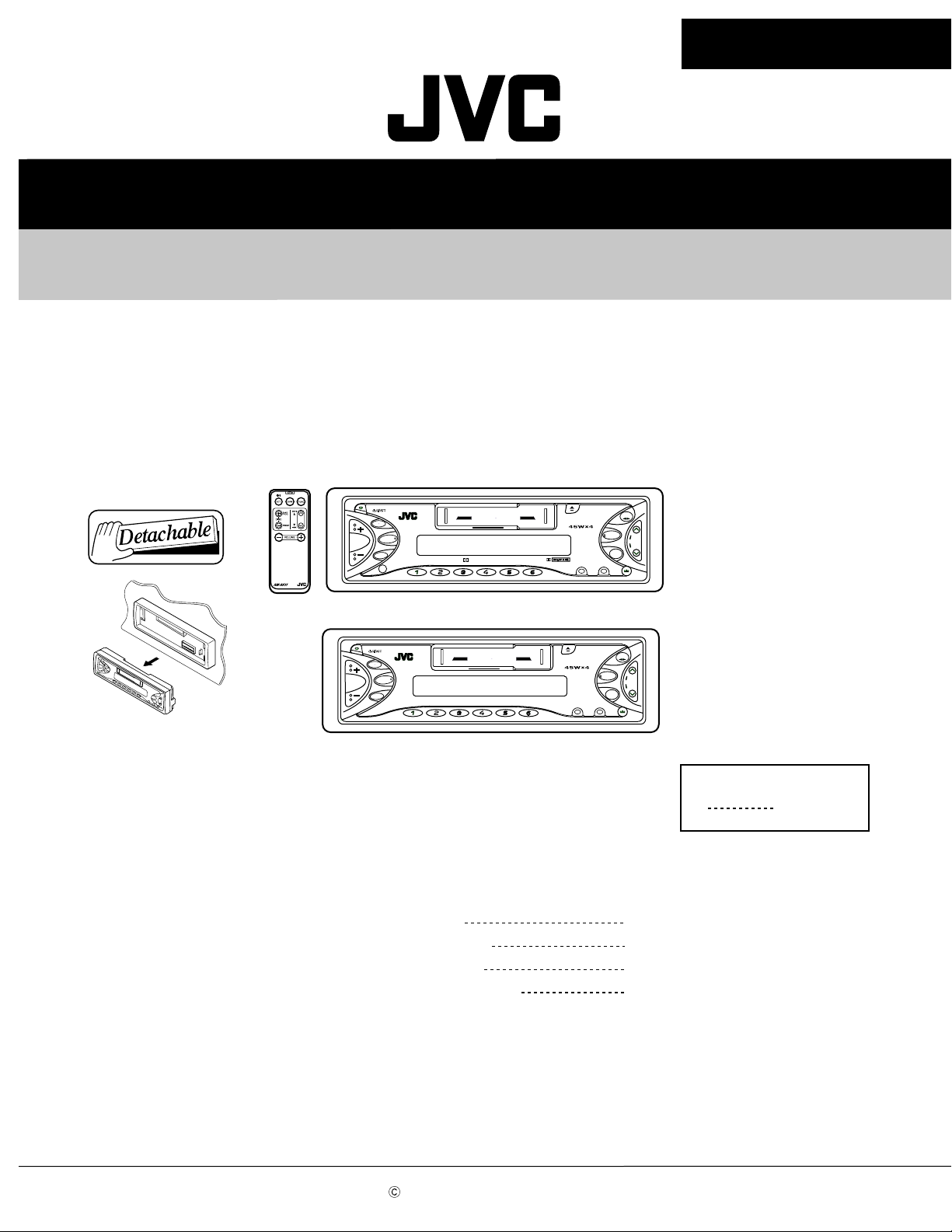
KS-FX711/KS-FX511
SERVICE MANUAL
CASSETTE RECEIVER
KS-FX711/KS-FX511
KS-FX711
Contents
LOUD
SEL
D
I
SP
7
CD CHANGER CONTROL
MO
10
9
8
KS-FX511
LOUD
SEL
D
I
SP
7
CD CHANGER CONTROL
MO
10
9
8
Safety precaution
Disassembly method
Adjustment method
Description of major ICs
11 12
RPT
11 12
RPT
KS-FX711
TAP
E
FM/AM
Multi
Music
Scan
RND
MODE
KS-FX511
Multi
Music
Scan
RND
MODE
SS
M
CDCH
SCM
TAP
E
FM/AM
SS
M
CDCH
SCM
Area Suffix
U Other areas
1-2
1-3
1-18
1-22
COPYRIGHT 2002 VICTOR COMPANY OF JAPAN, LTD.
No.49713
Mar. 2002
Page 2

KS-FX711/KS-FX511
Safety precaution
!
Burrs formed during molding may be left over on some parts of the chassis. Therefore,
pay attention to such burrs in the case of preforming repair of this system.
1-2
Page 3
Disassembly method
<Main body>
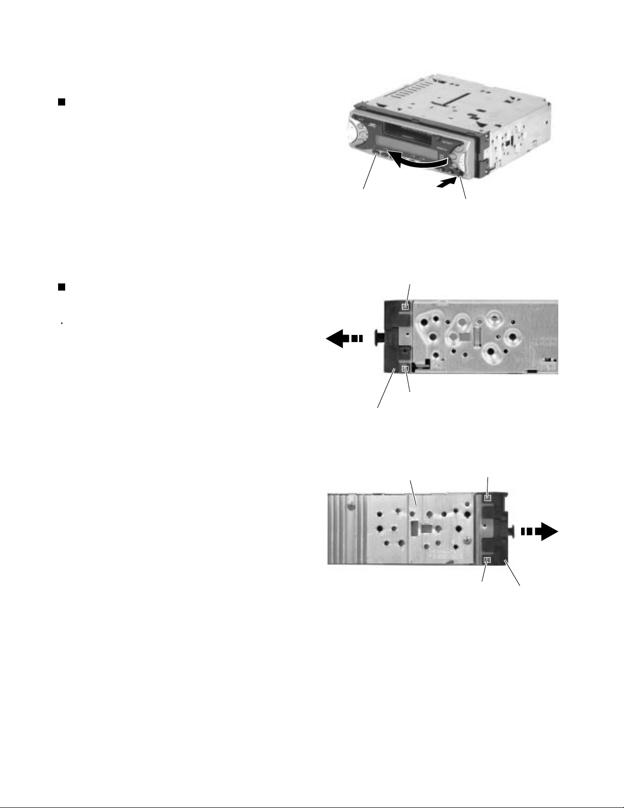
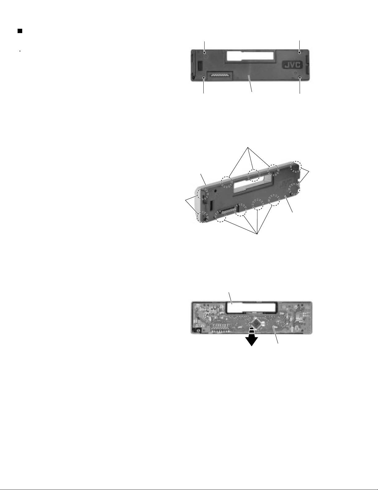
Removing the front panel assembly
(See Fig.1)
1.
Press the eject button in the lower right part of the
front panel. Remove the front panel assembly from
the body.
KS-FX711/KS-FX511
Front panel assembly
Eject button
Fig.1
Removing the front chassis assembly
(See Fig.2 and 3)
Prior to performing the following procedure, remove
the front panel assembly.
1.
Release the four joint tabs a on both sides of the
front chassis assembly and remove the front chassis
assembly toward the front.
Tab a
Tab a
Front chassis assembly
Heat sink
Fig.2
Tab a
Fig.3
Tab a
Front chassis
assembly
1-3
Page 4
KS-FX711/KS-FX511
Removing the heat sink (See Fig.4)
1.
Remove the three screws A on the left side of the
body.
Removing the bottom cover
(See Fig.5 and 6)
Prior to performing the following procedure, remove
the front panel assembly, the front chassis assembly
and the heat sink.
1.
Turn over the body and unjoint the four joints b and
joints c with the bottom cover and the body using a
screwdriver.
CAUTION:
When disengaging the joint c using a
screwdriver, do not damage or break the
board.
AA
Joints b
Joint c
Bottom cover
Heat sink
Fig.4
Bottom cover
Joints b
Rear panel
Fig.5
Joints c
1-4
Joints b
Joint c
Rear panel
Fig.6
Page 5
KS-FX711/KS-FX511
Removing the main board
(See Fig.7)
Prior to performing the following procedure, remove
the front panel assembly, the front chassis assembly,
the heat sink and the bottom cover.
1.
Remove the screw B, the five screws C and the two
screws D attaching the rear bracket on the back of
the body. Remove the rear bracket.
D
Rear bracket
E
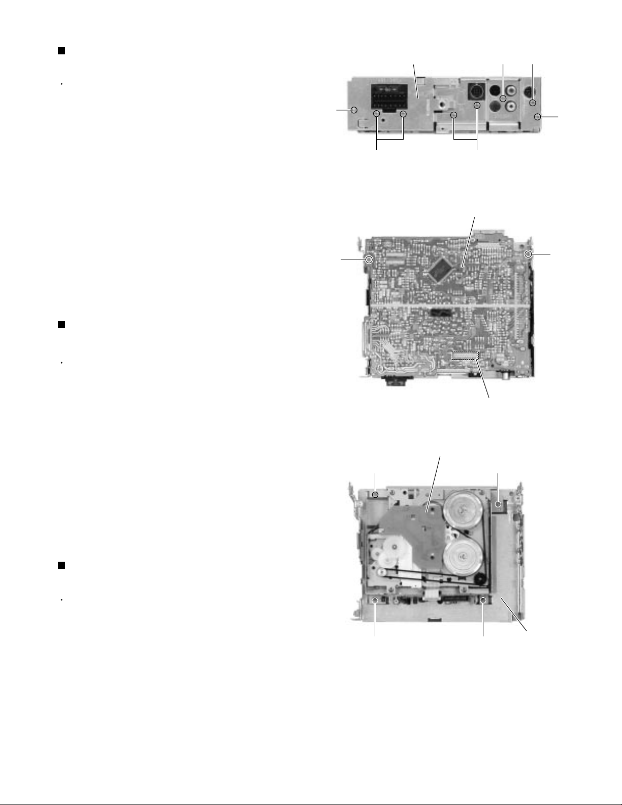
Removing the main amplifier board assembly
(See Fig.8)
Fig.7
CC
Main board
B
C
D
E
Prior to performing the following procedure, remove
the front chassis, the heat sink, bottom cover and the
rear panel.
1.
Remove the two screws E attaching the main
amplifier board assembly on the top cover.
2.
Disconnect connector CP701 on the main amplifier
board assembly from the cassette mechanism
assembly.
Cassette mechanism assembly
F
Removing the cassette mechanism assembly
(See Fig.9)
Prior to performing the following procedure, remove
the front chassis, the heat sink, bottom cover and the
main amplifier board assembly.
1.
Remove the four screws F attaching the cassette
mechanism assembly from the top cover.
CN701
Fig.8
F
Top chassis
FF
Fig.9
1-5
Page 6
KS-FX711/KS-FX511
Removing the control switch board
(See Fig.10 to 12)
Prior to performing the following procedure, remove
the front panel assembly.
1.
Remove the four screws G attaching the rear cover
on the back of the front panel assembly.
2.
Unjoint the eleven joints d with the front panel and
the rear cover.
3.
Remove the control switch board on the back of the
front panel.
Joints d
G
G
Front panel
Rear cover
Fig.10
Joints d
G
G
Joints d
Front panel
Rear cover
Joints d
Fig.11
Control switch board
Fig.12
1-6
Page 7
KS-FX711/KS-FX511
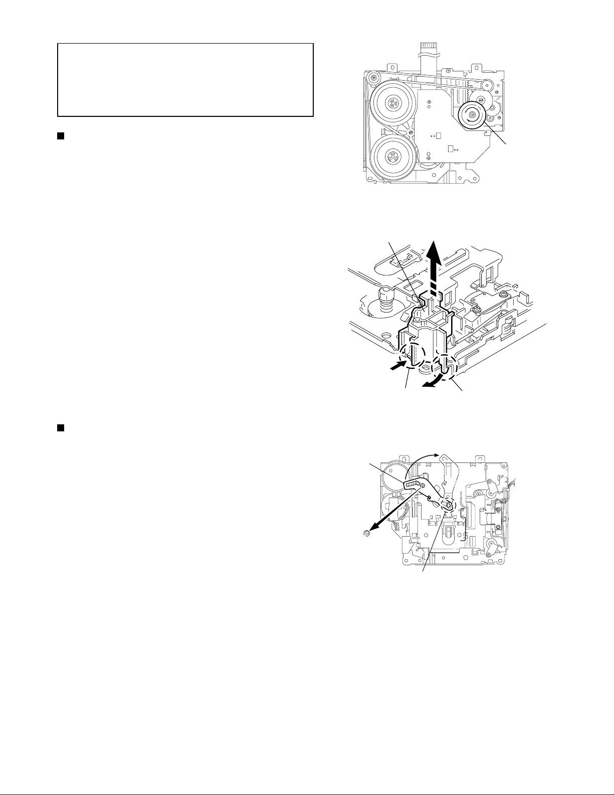
REFERENCE:
Prior to performing the following
procedures, turn the mode gear on the
bottom of the body until the respective part
comes to the EJECT position (Refer to
Fig.1).
Removing the cassette guide (See Fig.2)
1.
Turn the mode gear to set to RVS play or
subsequent mode.
2.
Remove the cassette guide from the main chassis
while releasing each two joint tabs a in the direction
of the arrow.
Mode gear
Fig.1
Cassette guide
Removing the load arm (See Fig.3)
1.
Remove the E-washer attaching the load arm.
2.
Move the load arm in the direction of the arrow and
release the joint b on the cassette catch.
Load arm
E-washer
Tab a
Joint b
Tab a
Fig.2
Fig.3
1-7
Page 8
KS-FX711/KS-FX511
Removing the cassette hanger assembly /
cassette holder (See Fig.4 to 7)
1.
Check the mode is set to EJECT. Push down the
front part of the cassette holder and move in the
direction of the arrow to release the joint c.
2.
Move the rear part of the cassette hanger assembly
in the direction of the arrow to release it from the two
joint bosses d.
3.
Release the holder stabilizer spring from the hooks e
and f, then pull out from the cassette hanger
assembly.
4.
Bring up the rear side of the cassette hanger
assembly to release the joint g and h.
5.
Pull out the cassette catch from the cassette hanger
assembly.
Cassette holder assembly
Side bracket
Joints c
Cassette holder assembly
Cassette stabilizer spring
Fig.4
Boss d
Cassette hanger assembly
Cassette hanger
assembly
Boss d
Cassette holder
assembly
Hook g
Fig.6
Hook f
Hook e
Fig.5
Cassette hanger assembly
Cassette catch
Cassette holder assembly
Cassette hanger assembly
Hook h
Fig.7
1-8
Page 9
KS-FX711/KS-FX511
Removing the side bracket assembly
(See Fig.8 to 10)
1.
Remove the screw A attaching the side bracket
assembly.
2.
Detach the front side of the side bracket assembly
upward and pull out forward to release the joint i and
j in the rear.
CAUTION:
CAUTION:
When reassembling, make sure that the
boss k of the main chassis is set in the
notch of the load rack under the side
bracket assembly. Do not reattach the
load rack on the boss k.
After reattaching the side bracket
assembly, confirm operation.
Side bracket assembly
Joint i
Joint j
A
Side bracket assembly
Fig.8
Side bracket assembly
Joint i
Joint j
Load rack
Load rack
Boss k
Boss k
Fig.9
Fig.10
1-9
Page 10
KS-FX711/KS-FX511
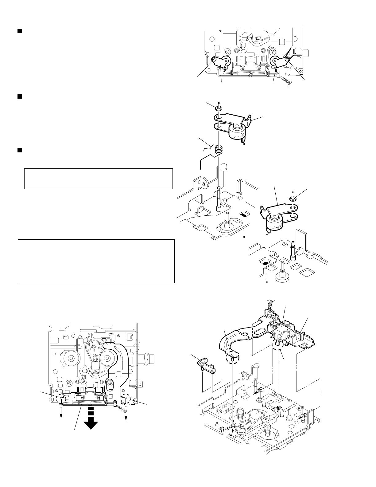
Removing the pinch arm (F) assembly
(See Fig.11 and 12)
1.
Remove the polywasher and pull out the pinch arm
(F) assembly.
2.
Remove the compulsion spring.
Removing the pinch arm (R) assembly
(See Fig.11 and 13)
1.
Remove the polywasher and pull out the pinch arm
(R) assembly.
Removing the slide chassis assembly
(See Fig.14 and 15)
Polywasher
Pinch arm
(R) assembly
Polywasher
Compulsion spring
Fig.11
Pinch arm
(F) assembly
Pinch arm (F) assembly
Polywasher
REFERENCE:
It is not necessary to remove the head
and the tape guide.
1.
Move the slide chassis assembly in the direction of
the arrow to release the two joints l and remove from
the main chassis.
2.
Remove the rack link.
CAUTION:
When reassembling, first reattach the rack
link, and next fit the boss m and hook n of
the slide chassis assembly to the hole of
the main chassis, and engage the two joints
l.
Rack link
Fig.12
Boss m
Pinch arm
(R) assembly
Fig.13
Head
Hook n
Polywasher
Tape guide
Joint l
Slide chassis assembly
1-10
Fig.14
Joint l
Fig.15
Page 11

KS-FX711/KS-FX511
Removing the head / tape guide
(See Fig.16 and 17)
REFERENCE:
1.
Remove the band attaching the wire to the head.
2.
Remove the two screws B, the head and the head
support spring.
3.
Remove the pinch arm spring from the tape guide.
4.
Remove the tape guide and the pinch spring arm.
CAUTION:
CAUTION:
It is not necessary to remove the slide
chassis assembly.
When reattaching the pinch arm spring, set
both end of it to the pinch spring arm (
remarked o).
When reattaching the head, set the wires
into the groove of the tape guide (Fig.16).
B
Slide chassis assembly
Head
Tape guide
Fig.16
B
Pinch arm spring
Head
Head support spring
Tape guide
Removing the flywheel assembly (F) & (R)
(See Fig.18 and 19)
REFERENCE:
1.
Remove the belt at the bottom.
2.
Remove the two polywashers on the upper side.
3.
Pull out each flywheel assembly downward.
Flywheel assembly (F)
It is not necessary to remove the slide
chassis assembly.
Belt
o
Pinch spring arm
o
Slid chassis assembly
Fig.17
Polywasher
Polywasher
Flywheel assembly (R)
Fig.18
Flywheel assembly (F)
Fig.19
Flywheel assembly (R)
1-11
Page 12

KS-FX711/KS-FX511
Disassembling the flywheel assembly (F)
(See Fig.20 and 21)
1.
Push and turn counterclockwise the spring holder (F)
to release the three joints p on the bottom of the
flywheel.
2.
The spring holder (F), the TU spring and the friction
gear play come off.
3.
Remove the polywasher and felt.
Flywheel assembly (F)
Joints p
Flywheel assembly (R)
Joints q
Disassembling the flywheel assembly (R)
(See Fig.20 and 22)
1.
Push and turn clockwise the spring holder (R) to
release the three joints q on the bottom of the
flywheel.
2.
The spring holder (R), the FF spring and the friction
gear FF come off.
3.
Remove the polywasher and the felt.
Removing the reel board
(See Fig.23 and 24)
1.
Remove the two screws C attaching the reel board.
2.
Move the reel board in the direction of the arrow to
release the joint r.
3.
Unsolder the wires if necessary.
CAUTION:
When reattaching, confirm operation of
the MODE switch and the ST-BY switch.
The mode position between EJECT and
ST-BY is optimum for reattaching.
Joint p
Fig.20
Polywasher
Polywasher
Spring holder (R)
Spring holder (F)
TU spring
Friction gear FF
Friction gear play
Felt
Flywheel assembly (F)
FF spring
Felt
Flywheel assembly (R)
Fig.21 Fig.22
Joint q
1-12
Connect the card wire extending from
the reel board to the FFC pad before
reattaching the reel board.
FFC pad
C
Reel board
C
Fig.23
Joint r
FFC pad
CT-1 switch
MODE switch
Soldering
ST-BY switch
Fig.24
Page 13

KS-FX711/KS-FX511
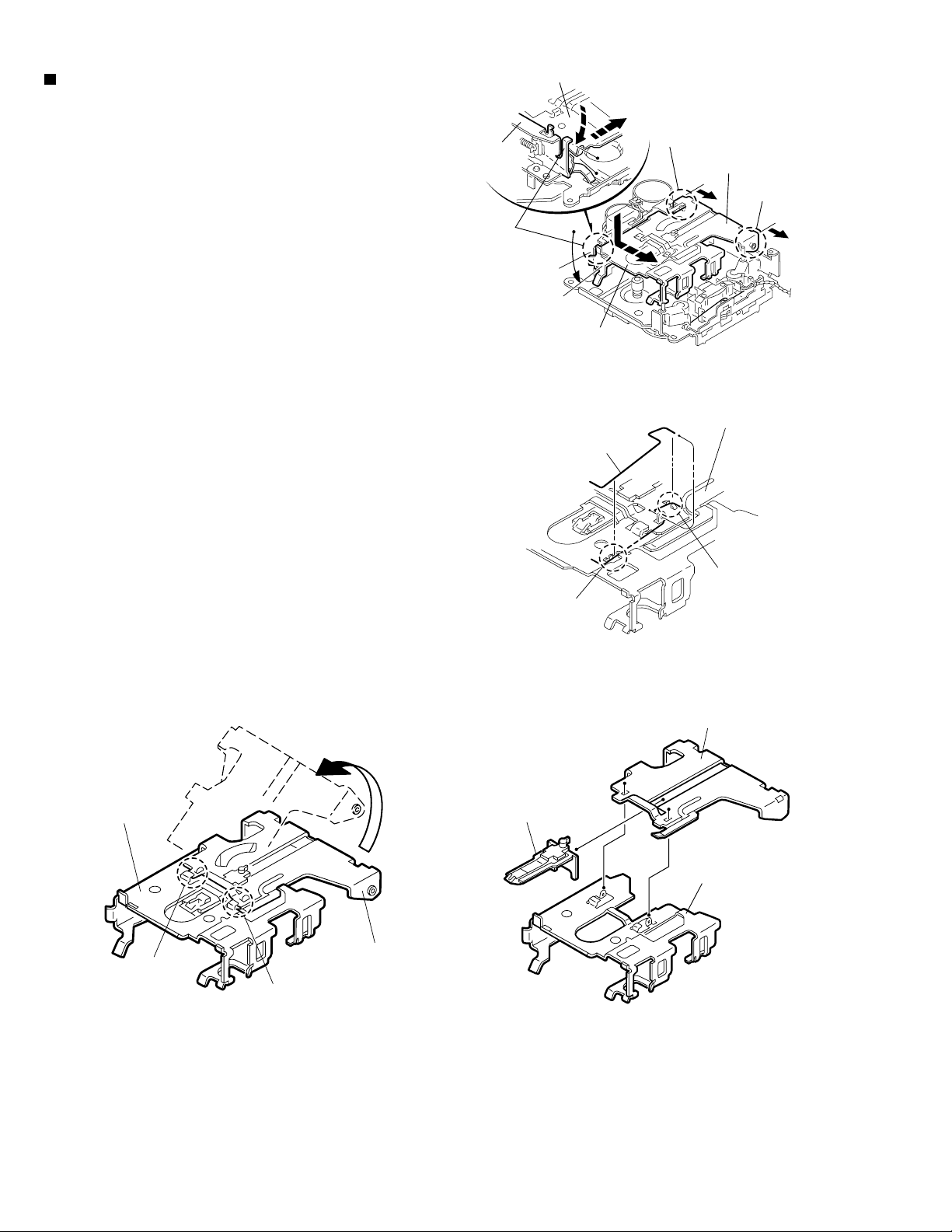
Removing the gear base arm / gear base
link assembly (See Fig.25 to 27)
1.
Move the gear base arm in the direction of the arrow.
2.
Insert a slotted screwdriver to the gear base spring
under the gear base arm, and release the gear base
arm upward from the boss on the gear base
assembly.
3.
Remove the gear base arm from the main chassis
while releasing the two joints s.
4.
Move the gear base link assemby in the direction of
the arrow to release the two joints t.
REFERENCE:
When reattaching the gear base arm,
make sure that the boss on the gear
base assembly is inside the gear base
spring.
Removing the FFC pad
(See Fig.27 and 29)
Gear base
link assembly
Gear base spring
Joint t
Gear base arm
Joints s
Hook u
FFC pad
Hook u
Joint t
Fig.25
Gear base arm
Screwdriver
1.
Push each joint hook u of the FFC pad and remove
toward the bottom.
Gear base link assembly
Fig.26
Gear base arm
Fig.27
FFC pad
1-13
Page 14

KS-FX711/KS-FX511
Removing the mode gear
(See Fig.28 and 31)
1.
Remove the polywasher on the bottom and pull out
the mode gear.
Removing the mode switch actuator
(See Fig.28, 29 and 31)
1.
Pull out the mode switch actuator at the bottom.
REFERENCE:
When reattaching the mode switch
actuator to the main chassis, make sure to
set on the shaft and insert v into the slot w.
Removing the direction link / direction
plate (See Fig.29 to 31)
1.
Remove the polywasher attaching the direction link.
2.
Bring up the direction link to release the three joints
x, y and z at a time.
3.
Move the direction plate in the direction of the arrow
to release the two joints a’.
REFERENCE:
When reattaching the direction plate,
engage the two joints a’ and move in the
direction of the arrow (Refer to Fig.30).
Mode switch actuator
Direction plate
Direction link
Fig.28
Direction plate
Joints a'
Joint z
Direction link
Slot w
Joint y
Polywasher
Fig.29
Direction plate Mode rack assembly
Joint b'
Mode gear
Polywasher
Mode rack assembly
Joint x
Joint b'
Joint c'
REFERENCE:
When reattaching the direction link,
move the direction plate in the direction
of the arrow and engage the three joint
x, y and z at a time (Refer to Fig.31).
Removing the mode rack assembly
(See Fig.29 and 30)
1.
Move the mode rack assembly in the direction of the
arrow to release the two joints b’ and the joint c’.
REFERENCE:
When reattaching, set the two b’ on the
bottom of the mode rack assembly into the
slots of the main chassis and move in the
direction of the arrow (See Fig.30).
Joints a'
Fig.30
Direction link
Mode switch actuator
Polywasher
v
Mode gear
Direction plate
Mode rack assembly
Fig.31
1-14
Page 15

KS-FX711/KS-FX511
Removing the gear base assembly / take
up gear / reflector gear (See Fig.32 to 34)
1.
Push in the pin d’ of the gear base assembly on the
upper side of the body and move the reflector gear
toward the bottom, then pull out.
2.
Remove the polywasher on the bottom and pull out
the take up gear.
3.
Move the gear base assembly in the direction of the
arrow to release it from the two slots e’ of the main
chassis.
REFERENCE:
The parts are damaged when removed.
Please replace with new ones.
Gear base assembly
Pin d'
Polywasher
Slot e'
Slot e'
Fig.32
Take up gear
Removing the reel driver / reel spindle
(See Fig.34)
1.
Draw out the reel driver from the shaft on the main
chassis and remove the reel driver spring and the
reel spindle respectively.
CAUTION:
The reel driver is damaged when
removed. Please replace with a new
one.
Reflector gear
Reel driver
Reel driver spring
Reel spindle
Main chassis
Fig.33
Reel driver
Reel driver spring
Reel spindle
Gear base assembly
Slots e’
Take up gear
Reflector gear
Polywasher
Fig.34
1-15
Page 16

KS-FX711/KS-FX511
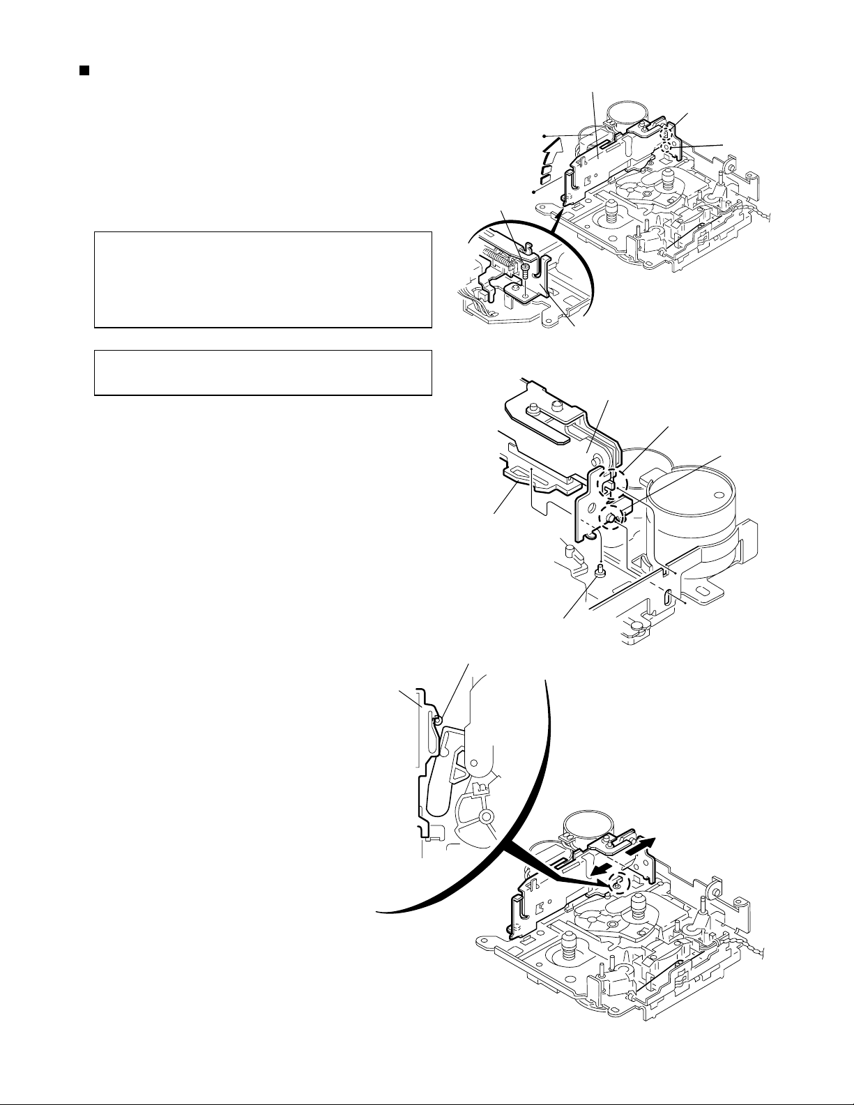
Removing the side bracket assembly
(See Fig.35 to 39)
1.
Remove the eject cam plate spring.
2.
Push the joint f‘ through the slot to remove the load
rack downward.
3.
Move the eject cam limiter in the direction of the
arrow to release it from the boss g’ of the side
bracket assembly and from the two joints h’.
4.
Move the eject cam plate in the direction of the arrow
to release the joint i’.
Joint f'
CAUTION:
Joint h'
When reassembling, confirm operation of
each part before reattaching the eject cam
plate spring.
Side bracket assembly
Boss g'
Eject cam limiter
Side bracket assembly
Joint h'
Joint f'
Eject cam plate spring
Joint h'
Load rack
Fig.35
Boss g'
Eject cam limiter
Eject cam plate
Fig.37
Joint h'
1-16
Fig.36
Side bracket assembly
Boss g'
Eject cam plate
Fig.38
Load rack
Joint i'
Side bracket assembly
Eject cam plate
Joint i'
Fig.39
Page 17

KS-FX711/KS-FX511
Removing the main motor assembly /
sub motor assembly (See Fig.40 to 42)
1.
Remove the belt at the bottom.
2.
Remove the polywasher and pull out the mode gear.
3.
Pull out the reduction gear (B).
4.
Remove the polywasher and pull out the reduction
gear (A).
5.
Remove the two screws D attaching the main motor
assembly.
6.
Remove the two screws E attaching the sub motor
assembly.
7.
Unsolder the wires on the reel board if necessary.
CAUTION:
When reassembling, adjust the length of the
wires extending from the sub motor
asswmbly by attaching them to the side of
the sub motor assembly with the wires
extending from the main motor assembly
using a spacer.
Belt
Reduction gear (B)
Reduction gear (B)
E
Polywasher
Fig.40
D
E
Mode gear
Polywasher
Reduction gear (A)
D
Main motor
assembly
Reduction
gear (A)
Polywasher
Sub motor
assembly
Spacer
Main motor assembly
Sub motor assembly
Main motor assembly
Sub motor assembly
Fig.41
Spacer
Fig.42
1-17
Page 18

KS-FX711/KS-FX511
Adjustment method
Test instruments reqired for adjustment
1. Digital osclloscope(100MHz)
2. Frequency Counter meter
3. Electric voltmeter
4. Wow & flutter meter
5. T est T apes
MC-109C
VT724.......................
VT739............For playback frequency measurement
VT712....For wow flutter & tape speed measurement
VT703..................... For head azimuth measurement
6. T orque gauge .................... Cassette type for CTG-N
...................
for TAPA CURL confirmation
(without Padd type)
for DOLBY level measurement
(mechanism adjustment)
Standard volume position
Balance and Bass,Treble volume .Fader
:Center(Indication"0")
Loudness,Dolby NR,Sound,Cruise:Off
Volume position is about 2V at speaker output with
following conditions.Playback the test tape VT721.
AM mode 531kHz to 1602kHz
FM mode 87.5 MHz to 108.0 MHz
Measuring conditions(Amplifier section)
Power supply voltage.............. DC14.4V (11V to 16V allowance)
Load impedance ........... 4 (4 to 8 allownce)
Line out level/impedance ...............................
2.0V/20k load (250 nWb/m)
1-18
Page 19

Arrangement of adjusting & test points
Cassette mechanism
(Surface)
Motor assembly
KS-FX711/KS-FX511
Tape speed adjust
Head section view
Azimuth screw A
(Forward)
Playback head
Azimuth screw B
(Reverse)
Azimuth screw B
(Reverse)
Azimuth screw A
(Forward)
Playback Head
1-19
Page 20

KS-FX711/KS-FX511
Arrangment of adjusting
Head amplifier board section (Reverse side)
R411
VR402
FSMW1093A
B409
R426
C423
R425
D401
1
T11
R424
IC402
VR402:Rch
(Dolby NR level
B407
C425
C424
Q401
R410
B406
D402
R401
R416
C419
C422
C413
C414
B408
C421
adj)
C418
R420
Q403
R412
11
R414
R415
R418
B411
B410
21
R413
R417
C417
B404
CJ403
2
C415
1
B413
C416
B403
(Dolby NR F
C412
1
IC401
31
C411
B405
B412
VR401
B402
R423
requency response adj)
B401
R408
C410
C409
R405
R406
C405
C406
R407
C407
C403
C408
R403
R402
C402
2
CJ401
1
C404
R404
C401
1
R422
Q402
VR401:Rch
Information for using a car audio service jig
1. We're advancing efforts to make our extension cords common for all car audio products.
Please use this type of extension cord as follows.
2. As a U-shape type top cover is employed, this type of extension cord is needed to check operation of the
mechanism assembly after disassembly.
3. Extension cord : EXTKSRT002-18P ( 18 pin extension cord ) For connection between mechanism assembly
and main board assembly .
Check for mechanism driving section such as motor ,etc..
Cassette mechanism
Disassembly method
1. Remove the bottom cover.
2. Remove the front panel assembly.
3. Remove the top cover .
4. Install the front panel.
5. Confirm that current is being carried by connecting
an extension cord jig.
Note
Available to connect to the CP701 connector when installing the front panel.
Extension cord
EXTKSRT002-18P
to Cassette mechanism
1-20
EXTKSRT002-18P
Main board
to Main board
Front panel assembly
Page 21

KS-FX711/KS-FX511
Mechanism adjustment section
Item Adjusting & Confirmation Methods Adjust Std. Value
1. Tape running
adjustment
2. Azimuth
adjustment
confirmation
a) At Forward playmode, using mirror tape, make adjustment
with Azimuth screw A and Azimuth screw B, without curl of 4
parts of head tape guide.
b) At Reverse play mode, using mirror tape, make adjustment
with Azimuth screw A and Azimuth screw B, without tape
curl of 4 parts of head guide.
c) At Forward / Reverse play mode, make confirmation of no
tape curl of 4 parts of head tape guide.
a) At forward play mode, make adjustment of peak of Lch / Rch
output with Azimuth screw A.
* For Oscilloscope litharge corrugation, set 45 as standard.
b) At Reverse play mode, make adjustment of peak of Lch / Rch
output with Azimuth screw B.
* For Oscilloscope litharge corrugation, set 45 as standard.
c) With AC volt meter confirm the difference of output for 4ch
between Lch / Rch at forward play mode and Lch / Rch
Reverse play mode being within 3.0dB.
d) After operation, make confirmation of Lch / Rch azimuth
output being within 1.0dB from adjustment value.
Azimuth
screw A
Azimuth
screw B
2.T ape Speed and
Wow & Flutter
HEAD
Tape guide
OK
HEAD TAPE
1.Check to see if the reading of the frequency counter & W ow
flutter meter is within 2940-3090 Hz( FWD/REV ), and less
than 0.35% ( JIS RMS ).
2.In case of out of specification, adjust the motor with a builtin volume resistor .
Tape curl NG
0
Phase
Built-in
volume resistor
45
T ape Speed
2940-3090Hz
Wow&Flutter
Less than
0.35%
(JIS RMS)
3.Playback
Frequency
response
1.Play the test tape ( VT724 : 1kHz ) back and set the volume
position at 2V .
2.Play the test tape ( VT739 )back and confirm 0 3dB at1kHz/
10kHz and -4+2dB at 1kHz/63Hz.
3.When 10kHz is out of specification, it will be necessary to
read adjust the azimuth.
Speaker out
1kHz/10kHz
: 0dB 3dB,
63Hz/1kHz
: -4dB+2dB,
1-21
Page 22

KS-FX711/KS-FX511
Description of major ICs
AN80T05 (IC901) : Power regulator
1.Terminal layout & Block diagram
Reference V oltage
ASO & Peak
Thermal
Protection
Current Protection
Pre
Drive
1 2 3 4 5 6 7 8 9 10 11 12
ILL
10V
2.Pin function
Pin
No.
1
2
3
4
5
6
7
8
9
10
11
12
Pre
Drive
MODE2 MODE1 STB VDD
5.6V
AMP
Out
AMP VCC ANT COM
Symbol Function
ILL10V
TUNER
FM/AM
PWR-CNT
5.6V
REMOTOE
MEMORY
10V power supply for illumination.
When 5V is input,becomes AM. and the antenna output is turned on.
When 5V is input,becomes AM. and the output of FM is switched.
When 5V is input, outputs to ILL,COM,and AMP. It is 0V usually.
5.6V power supply.
Power supply supply to remote amplifier
Back up. connects with ACC with it.
NC
9V
AMVCC
FMVCC
GND
8.7V power supply.
The power supply of 8.7V to AM.
The power supply of 8.7V to FM.
Ground
AMP
Out
Pre
Drive
Pre
Drive
8.7VAM8.7VFM8.7V
Pre
Drive
GND
1-22
Page 23

KS-FX711/KS-FX511
CXA2560Q (IC401) : Dolb y B type noise reduction system with play back equalizer amp.
1.Pin layout & block diagram
PBFB2
31
PBRIN2
32
PBGND
33
PBFIN2
34
VCT
35
45k
PBREF
36
PBFIN1
37
PBGND
38
PBRIN1
39
PBFB1
40
2. Pin function
Pin No. Symbol
1
2
3
4
5
6
7
8
9
10
11
12
13
14
15
16
17
18
19
20
21
22
23
24
PBTC1
PBOUT1
OUTREF1
TAPEIN1
Vcc
NC
LINEOUT1
TCH1
NC
MSLPF
G2FB
G1FB
MSTC
MSOUT
NC
NRSW
MUTESW
TAPESW
DRSW
MSMODE
MSSW
NC
TCH2
LINEOUT2
PBTC2
30 29 28
7k/12k
12345
PBTC1
300k
30k
30k
300k
7k/12k
F2
F1
PBOUT2
+
+
-
PBOUT1
OUTREF2
27
70 /120
1
1
70 /120
OUTREF1
TAPEIN2
100k
100k
TAPEIN1
GND
26
T2
T1
Vcc
I/O Function
Playback equalizer amplifier
capacitance
Playback equalizer amplifier
O
output
Output reference
O
TAPE input
I
Power supply
-
Line output
O
Time constant for the HLS
-
Cut-off frequency adjustment
of the music sensor LPF
Music signal interval detection
Music signal interval detection
Time constant for detecting
music signal interval
Music sensor out
O
No use
Dolby NR control
I
Mute function control
I
Playback equalizer amplifier
I
control
Head select control
I
Music sensor mode control
I
Music sensor control
I
Time constant for the HLS
Line output
O
LPF
DIREF
25
BIAS
MUTE
TAPE EQ
FWD/RVS
Vcc
+
-
6
NC
LINEOUT2
23 22 21
24
OFF/B
+
-
F3
OFF/B
-
+
8910
7
LINEOUT1
TCH2
NR
NR
TCH1
NC
MS MODE
NR MODE
MS ON/
DET
NC
OFF
MSSW
MSLPF
20
19
18
17
16
15
14
13
12
11
MSMODE
DRSW
TAPESW
MUTESW
NRSW
NC
MSOUT
MSTC
G1FB
G2FB
Pin No. Symbol
25
26
27
28
29
30
31
32
33
34
35
36
37
38
39
40
DIREF
GND
TAPEIN2
OUTREF2
PBOUT2
PBTC2
PBFB2
PBRIN2
PBGND
PBFIN2
VCT
PBREF
PBFIN1
PBGND
PBRIN1
PBFB1
I/O Function
-
Resistance for setting the
reference
-
Ground
I
TAPE input
O
Output reference
O
Playback equalizer amplifier
output
-
Playback equalizer amplifier
capacitance
I
Playback equalizer amplifier
feedback
I
Playback equalizer amplifier
input
-
Playback equalizer amplifier
ground
I
Playback equalizer amplifier
input
O
Center
O
Playback equalizer amplifier
reference
I
Playback equalizer amplifier
input
-
Playback equalizer amplifier
ground
I
Playback equalizer amplifier
input
I
Playback equalizer amplifier
feedback
1-23
Page 24

KS-FX711/KS-FX511
LA4743K(IC301):Power AMP
1.Block diagram
IN 1
TAB
IN 2
+
0.22 F
+
0.22 F
11
1
12
Vcc 1/2 Vcc 3/4
6 20
-
+
Protective
circuit
-
+
2200 F 0.022 F
+
9
-
7
+
OUT 1+
OUT 1-
PWR GND1
8
+
OUT 2+
5
-
OUT 2-
3
PWR GND2
2
ST BY
R.F
47 F
IN 3
PRE GND
IN 4
+5V
ST ON
+
0.22 F
N.C
+
0.22 F
4
Stand by
Switch
Mute
10
+
Ripple
Filter
Mute
22
circuit
3.3 F
+
15
-
+
-
17
19
10K
+
OUT 3+
OUT 3-
Low Level
Mute ON
25
18
21
23
PWR GND3
OUT 4+
OUT 4-
13
14
Protective
circuit
-
+
+
-
1-24
ON TIME C
22 F
Muting &
16
+
ON Time Control
Circuit
PWR GND4
24
Page 25

2.Terminal layout
KS-FX711/KS-FX511
3.Pin function
1
2
3
4
5
6
7
8
9
10
11
12
13
14
15
16
17
18
19
20
21
22
23
24
25
SymbolPin No. Function
TAB
GND
RFOSTBY
RFO+
VCC1/2
RROGND
RRO+
Vref
RRIN
RFIN
SGND
LFIN
LRIN
ONTIME
LRO+
GND
LROVCC
LFO+
MUTE
LFOGND
NC
Header of IC
Power GND
Outpur(-) for front Rch
Stand by input
Output (+) for front Rch
Power input
Output (-) for rear Rch
Power GND
Output (+) for rear Rch
Ripple filter
Rear Rch input
Front Rch input
Signal GND
Front Lch input
Rear Lch input
Power on time control
Output (+) for rear Lch
Power GND
Output (-) for rear Lch
Power input
Output (+) for front
Muting control input
Output (-) for front
Power GND
No connection
LA4743K
1-25
Page 26

KS-FX711/KS-FX511
LC72366-9A74 (IC701) : Micro controller
1. Pin layout
25
~
40
2. Pin function
1
2
3
4
5
6
7
8
9
10
11
12
13
14
15
16
17
18
19
20
21
22
23
24
25
26
27
28
29
30
31
32
33
34
35
36
37
38
39
40
J-BUS SCK
DIMMER IN
TUNER ILLUM
TAPE ILLUM
DIMMER OUT
FF/REW MODE
SEEK/STOP
RADIO/TAPE
BEEP LEVEL
24 ~ 1
41 ~ 64
Symbol FunctionPin No.
XIN
GND
J-BUS SI
J-BUS SO
J-BUS I/O
NC
LCD SO
LCD SCK
LCD CE
EVOL SO
EVOL SCK
NC
CD ILLUM
NC
OPEN
NC
NC
NC
NC
KS1
KS0
K3
K2
K1
K0
Vdd
TEST
MONO
PWR-CNT
ACC
KICK
80
65
~
I/O
I
Crystal oscillator input port
-
Connect to GND
I
Data input for J-BUS information
O
Data output for J-BUS information
O
Clock output for J-BUS information
O
Switching signal output for J-BUS information I/O, H:Out L:In
-
None connection
O
Data output for LCD driver
O
Information clock output for LCD driver data
O
Chip enable output for LCD driver
-
None connection
O
Data output for electrical volume
O
Clock output for electrical volume information
-
Non connection
-
Non connection
-
Non connection
-
Non connection
-
Non connection
-
Non connection
-
Non connection
-
Non connection
-
Non connection
-
Non connection
-
Non connection
-
Non connection
O
Diode matrix output port for initial establishing
I
Diode matrix output port for initial establishing
I
Diode matrix output port for initial establishing
-
Non connection
I
Diode matrix output port for initial establishing
-
5V power supply port (+B)
I
Turn on all light indicator of LCD, L: All light a LED indicator
O
FF/REW mode select signal output
O
H:Auto seek, L: Stop Use both as IF count REQ and Seek/Stop
O
Forced monaural output port, H:Turn on Forced monaural
-
Non connection
-
Non connection
O
"H" : Turn on power
-
Non connection
-
Non connection
1-26
Page 27

41
42
43
44
45
46
47
48
49
50
51
52
53
54
55
56
57
58
59
60
61
62
LEVELMETER
63
64
65
66
67
68
69
AM IF COUNT
70
FM IF COUNT
71
72
73
74
75
76
77
78
79
80
MOTOR
SUBMO+
SUBMO-
BEEP
TAPE IN
STANDBY
REEL
MODE
F/R
MS
SD/ST
DETACH
NC
NC
J-BUS INT
REMOCON
FM/AM
DOLBY
NC
MUTE
MEM DET
S.METER
KEY2
KEY1
KEY0
ACCDET
SENSE
NC
NC
Vdd
AM OSC
FM OSC
VSS
NC
E0
TEST1
XOUT
I/OPort Name FunctionPin No.
Main motor output, H:Transport L: Stop
O
Sub-motor output(+), Loading direction to transport output
O
Sub-motor output(-), Eject direction to transport output
O
Non connection
Switch for detecting to input cassette, L: Cassette in
I
Switch for detecting standby position
I
Switch for detecting tape end position
I
Detecting mode position input
I
Switch for detecting forward/reverse , H:FWD L:REV
I
MS input port,
I
Station detector, Stereo signal input, H:SD
I
Front panel detect
O
Non connection
Non connection
Cut in signal detecting port from J-Bus information
I
Remocon input
I
FM/AM mode switching signal port, H:FM L:AM
O
Dolby NR control
O
Non connection
Mute output port, L:Mute
O
Back-up power supply detecting port, H:input L:no input
I
Pressure voice level voltage input for level meter.
I
S meter voltage input
I
Key 2 input port
I
Key 1 input port
I
Key 0 input port
I
Hold port for Acc detecting, L: Hold mode
I
Voltage sensor port
I
Non connection
FM frequency detecting
I
Non connection
Non connection
5V power supply (+B)
Non connection
I
FM limited signal input
I
Ground port for power supply
Non connection
Error signal output port for PLL
O
Test port for LSI, To connect ground
-
4.5MHz crystal oscillator output
O
KS-FX711/KS-FX511
LC72366-9A74(2/2)
1-27
Page 28

KS-FX711/KS-FX511
HD74HC126P (IC801) : Changer control
1.Pin arrangement 2. Pin function
11C
21A
31Y
42C
52A
62Y
7GND
3. Block diagram
1A
( TOP VIEW )
14
13
12
11
10
9
8
Vcc
4C
4A
4Y
3C
3A
3Y
Input Output
CA
X
LLH
HH H
Y
ZL
1Y
1C
2A
2C
3A
3C
4A
2Y
3Y
4Y
1-28
4C
Page 29

LC75823W (IC601) : LCD driver
1. Pin Layout & Symbol
CL
OSC
64 63 62 61 60 59 58 57 56 55 54 53 52 51 50 49
1
2
3
S3
4
S4
5
S5
6
S6
7
S7
8
S8
9
S9
S10
S11
S12
S13
S14
S15
S16
10
11
12
13
14
15
16
17 18 19 20 21 22 23 24 25 26 27 28 29 30 31 32
INH
VDD
COM3
COM2
COM1
S52
S51
S50
S49
48
47
46
45
44
43
42
41
40
39
38
37
36
35
34
33
KS-FX711/KS-FX511
S48
S47
S46
S45
S44
S43
S42
S41
S40
S39
S38
S37
S36
S35
S34
S33
2. Pin Function
Pin No.
3 to 52
53 to 55
S3 to S52
COM1 to COM3
56
57
60
61
62
63
Symbol
VDD
INH
Vss
OSC
CE
CL
S17
S18
S19
S20
S21
S22
S23
S24
S25
S26
S27
S28
S29
S30
S31
S32
I/O
O
Segment output pins used to display data transferred
Function
by serial data input.
O
Common driver output pins. The frame frequency is given
by : t0=(fosc/384)Hz.
--
Power supply connection. Provide a voltage of between
4.5 and 6.0V.
I
Display turning off input pin.
INT="L" (Vss) ----- off (S1 to S52, COM1 to COM3="L"
INT="H" (VDD)----- on
Serial data can be transferred in display off mode.
--
Power supply connection. Connect to GND.
I/O
Oscillator connection.
An oscillator circuit is formed by connecting an external
resistor and capacitor at this pin.
Serial data CE : Chip enable
interface connection
I
to the controller. CL : Sync clock
64
DI
DI : Transfer data
1-29
Page 30

KS-FX711/KS-FX511
TEA6320T-X (IC161) : E.volume
1.Pin layout
2.Block diagram
10 8 9 7 6
5
12
SDA
1
GND
2
OUTLR
OUTLF
MUTE
TL
B2L
B1L
IVL
ILL
QSL
IDL
ICL
IMD
IBL
IAL
3
4
5
6
7
8
9
10
11
12
13
14
15
16
3.Pin functions
Pin
Symbol
No.
SDA
1
SCL
32
VCC
31
OUTRR
30
OUTRF
29
TR
28
B2R
27
B1R
26
IVR
25
ILR
24
QSR
23
IDR
22
Vref
21
ICR
CD-CH
TAPE
TUNER
20
19
18
17
CAP
IBR
IAR
I/O
Serial data input/output.
I/O
MUTE
21
31
2
19
16
15
13
11
14
22
20
18
17
Functions Functions
POWER
SUPPLY
SOURCE
SELECTOR
23 25 24 26 27 28
VOLUME 1
+20 to -31 dB
LOUDNESS
LEFT
VOLUME 1
+20 to -31 dB
LOUDNESS
RIGHT
Pin
No.
17
Symbol
IAR
BASS
LEFT
+15 dB
LOGIC
BASS
RIGHT
+15 dB
I/O
I
Input A right source.
TREBLE
LEFT
+12 dB
TREBLE
RIGHT
+12 dB
FUNCTION
ZERO CROSS
DETECTOR
VOLUME 2
0 to 55 dB
BALANCE
FENDER REAR
VOLUME 2
0 to 55 dB
BALANCE
FENDER FRONT
HC BUS
REC
VOLUME 2
0 to -55dB
BALANCE
FENDER FRONT
VOLUME 2
0 to -55dB
BALANCE
FENDER REAR
3
4
32
1
29
30
2
3
4
5
6
7
8
9
10
11
12
13
14
15
16
GND
OUTLR
OUTLF
TL
B2L
B1L
IVL
ILL
QSL
IDL
MUTE
ICL
IMO
IBL
IAL
Ground.
output left rear.
O
output left front.
O
Treble control capacitor left channel or
I
input from an external equalizer.
Bass control capacitor left channel or
-
output to an external equalizer.
Bass control capacitor left channel.
Input volume 1. left control part.
I
Input loudness. left control part.
I
Output source selector. left channel.
O
Not used
Not used
Input C left source.
I
Not used
Input B left source.
I
Input A left source.
I
18
19
20
21
22
23
24
25
26
27
28
29
30
31
32
IBR
CAP
ICR
Vref
IDR
QSR
ILR
IVR
B1R
B2R
TR
OUTRF
OUTRR
Vcc
SCL
I
Input B right source.
-
Electronic filtering for supply.
I
Input C right source.
-
Reference voltage (0.5Vcc)
-
Not used
O
Output source selector right channel.
I
Input loudness right channel.
I
Input volume 1. right control part.
-
Bass control capacitor right channel
Bass control capacitor right channel or
O
output to an external equalizer.
Treble control capacitor right channel or
I
input from an external equalizer.
O
Output right front.
O
Output right rear.
-
Supply voltage.
I
Serial clock input.
1-30
Page 31

RPM6938-SV4(IC652) : LCD driver
1.Block diagram
KS-FX711/KS-FX511
AMP
I/V
conversion
PD
magnetic shield
KIA7810PI (IC902) : Regulator
1.Pin layout 2.Block diagram
R4 R18
1 2 3
Q12
R5
Z1
R6
R7
BPF
fo
trimming
circuit
R1
Q1
Q13
AGC
Q8
Q10
Q5
Q7
Detector
R8
Q6
R15
R2
Q2
Q14
C1
Q4
R9
Q9
Q15
R16
Vcc
Comp
Q3
Q11
R13
R21
R17
22k
Q16
R12
Vcc
Rout
GND
1 INPUT
Q17
R11
3 OUTPUT
R20
R19
LB1641 (IC402) : DC motor driver
1. Pin layout
1 2 3 4 5 6 7 8 9
GNDOUT1 P1
VZ IN1 IN2
VCC1
VCC2 P2
R10 R3
2. Pin function
10
OUT2
R14
Input Output
IN1 IN2 OUT1 OUT2
0 0 0 0
1 0 1 0
0 1 0 1
1 1 0 0
2 GND
Mode
Brake
CLOCKWISE
COUNTER-CLOCKWISE
Brake
1-31
Page 32

KS-FX711/KS-FX511
VICTOR COMPANY OF JAPAN, LIMITED
MOBILE ELECTRONICS DIVISION
PERSONAL & MOBILE NETWORK BUSINESS UNIT. 10-1,1Chome,Ohwatari-machi,Maebashi-city,371-8543,Japan
(No.49713)
200203
 Loading...