

Page 1
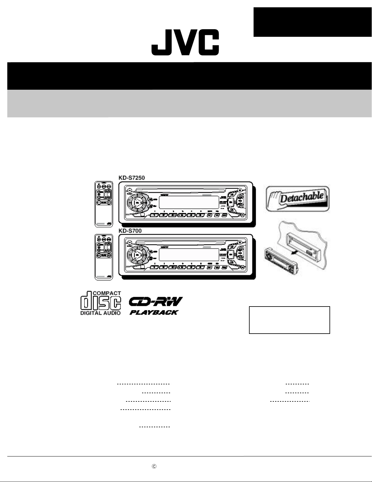
KD-S700GN/KD-S700BU
SERVICE MANUAL
CD RECEIVER
KD-S700GN/KD-S700BU
KD-S7250
KD-S7250
Contents
Safety precaution
Preventing static electricity
Disassembly method
Adjustment method
Flow of functional
operation unit TOC read
COPYRIGHT 2001 VICTOR COMPANY OF JAPAN, LTD.
1-2
1-3
1-4
1-11
1-12
Area Suffix
J ----Northern America
Maintenance of laser pickup
Replacement of laser pickup
Discription of major ICs
1-14
1-14
1-15
No.49670
Dec. 2001
Page 2
KD-S700GN/KD-S700BU
KD-S7250
Safety precaution
!
!
Burrs formed during molding may be left over on some parts of the chassis. Therefore,
pay attention to such burrs in the case of preforming repair of this system.
Please use enough caution not to see the beam directly or touch it in case of an
adjustment or operation check.
1-2
Page 3
KD-S700GN/KD-S700BU
KD-S7250
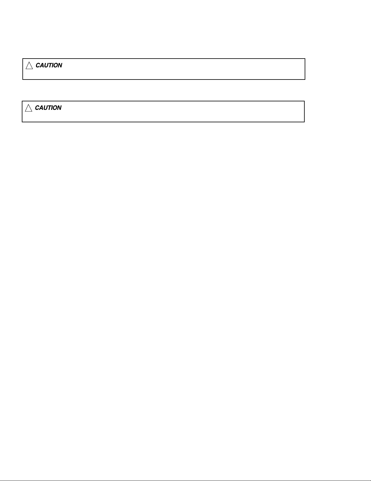
Preventing static electricity
1.Grounding to prevent damage by static electricity
Electrostatic discharge (ESD), which occurs when static electricity stored in the body, fabric, etc. is discharged,
can destroy the laser diode in the traverse unit (optical pickup). Take care to prevent this when performing repairs.
2.About the earth processing for the destruction prevention by static electricity
Static electricity in the work area can destroy the optical pickup (laser diode) in devices such as CD players.
Be careful to use proper grounding in the area where repairs are being performed.
2-1 Ground the workbench
Ground the workbench by laying conductive material (such as a conductive sheet) or an iron plate over
it before placing the traverse unit (optical pickup) on it.
2-2 Ground yourself
Use an anti-static wrist strap to release any static electricity built up in your body.
(caption)
Anti-static wrist strap
Conductive material
3. Handling the optical pickup
1. In order to maintain quality during transport and before installation, both sides of the laser diode on the
replacement optical pickup are shorted. After replacement, return the shorted parts to their original condition.
(Refer to the text.)
2. Do not use a tester to check the condition of the laser diode in the optical pickup. The tester's internal power
source can easily destroy the laser diode.
(conductive sheet) or iron plate
4.Handling the traverse unit (optical pickup)
1. Do not subject the traverse unit (optical pickup) to strong shocks, as it is a sensitive, complex unit.
2. Cut off the shorted part of the flexible cable using nippers, etc. after replacing the optical pickup. For specific
details, refer to the replacement procedure in the text. Remove the anti-static pin when replacing the traverse
unit. Be careful not to take too long a time when attaching it to the connector.
3. Handle the flexible cable carefully as it may break when subjected to strong force.
4. It is not possible to adjust the semi-fixed resistor that adjusts the laser power. Do not turn it
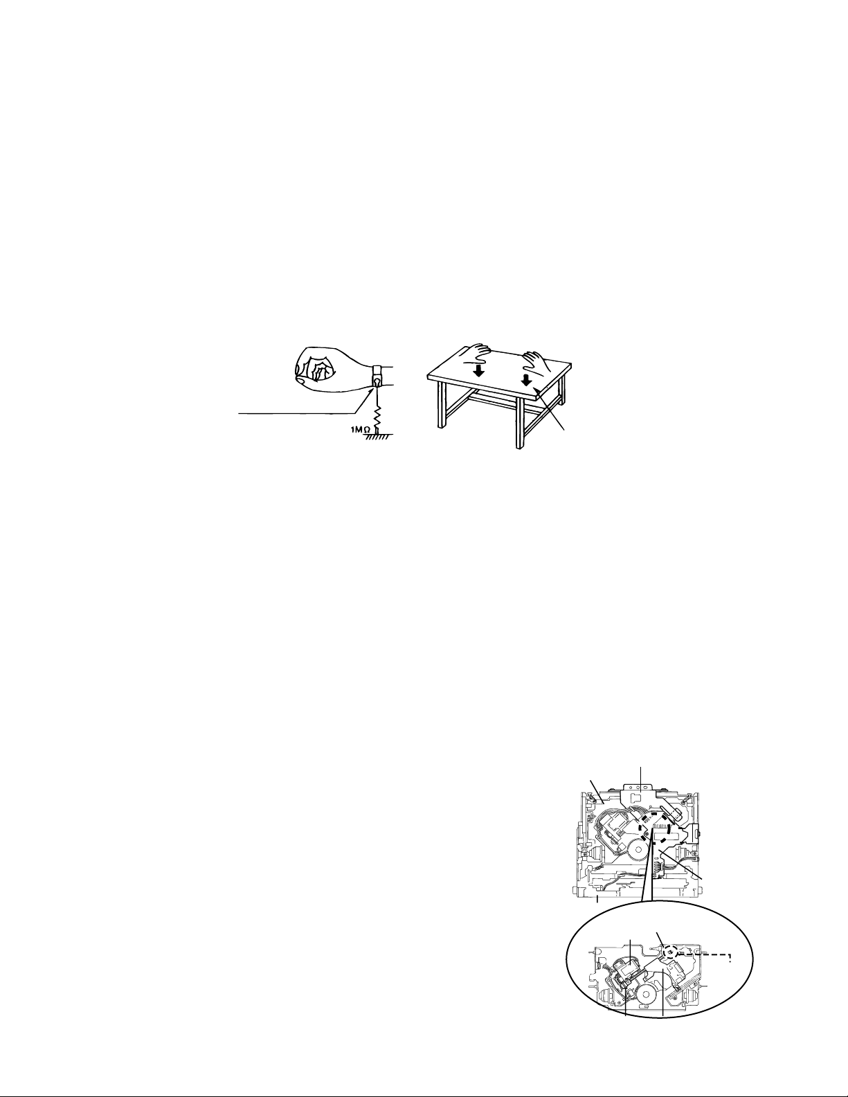
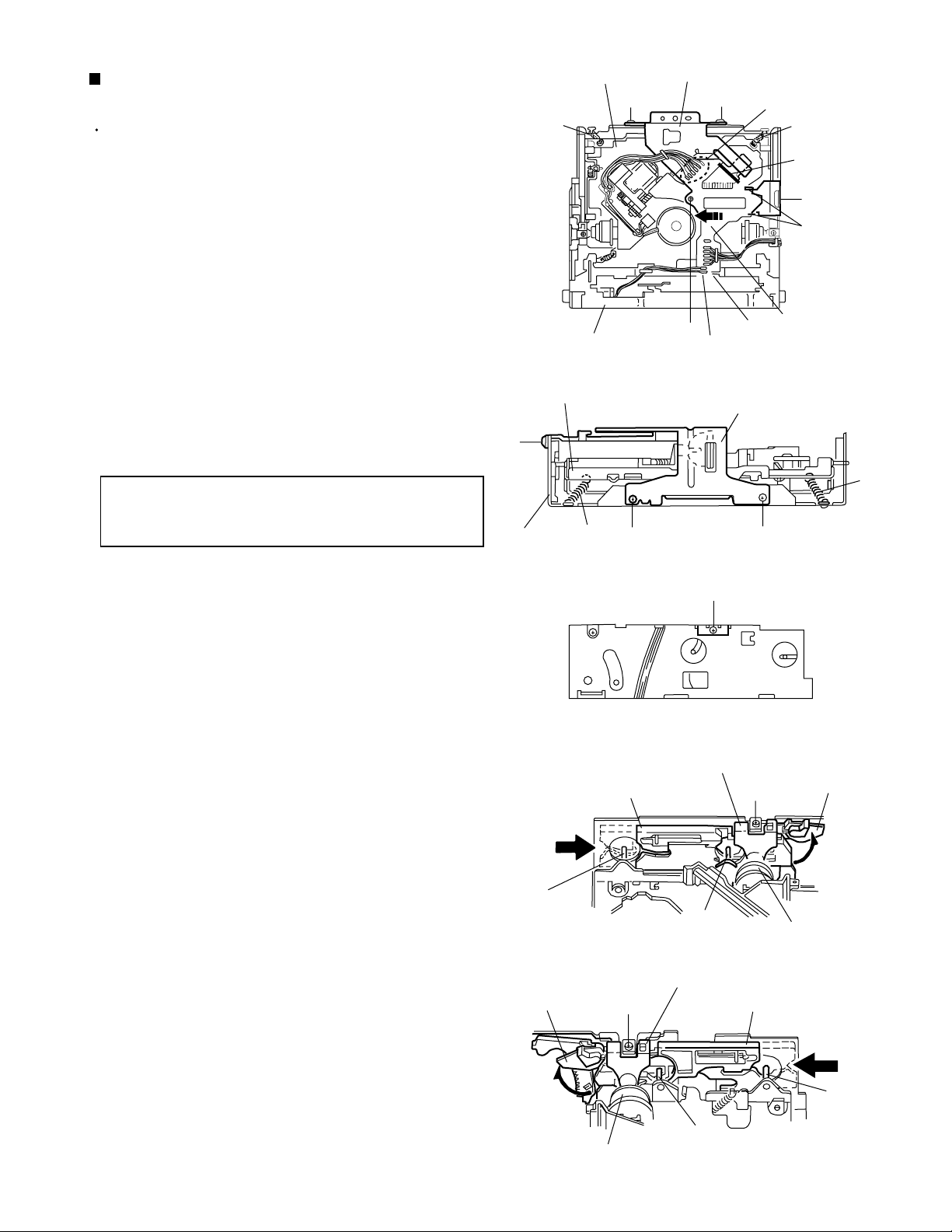
CD mechanism ass’y
Damper bracket
Attention when traverse unit is decomposed
*Please refer to "Disassembly method" in the text for pick-up and how to
detach the substrate.
1.Solder is put up before the card wire is removed from connector on
the CD substrate as shown in Figure.
(When the wire is removed without putting up solder, the CD pick-up
assembly might destroy.)
2.Please remove solder after connecting the card wire with
when you install picking up in the substrate.
Front bracket
Feed motor ass’y
FD screw
CD mechanism
control board
Soldering
FD gear
Pickup unit
1-3
Page 4
KD-S700GN/KD-S700BU
KD-S7250
Disassembly method
<Main body>
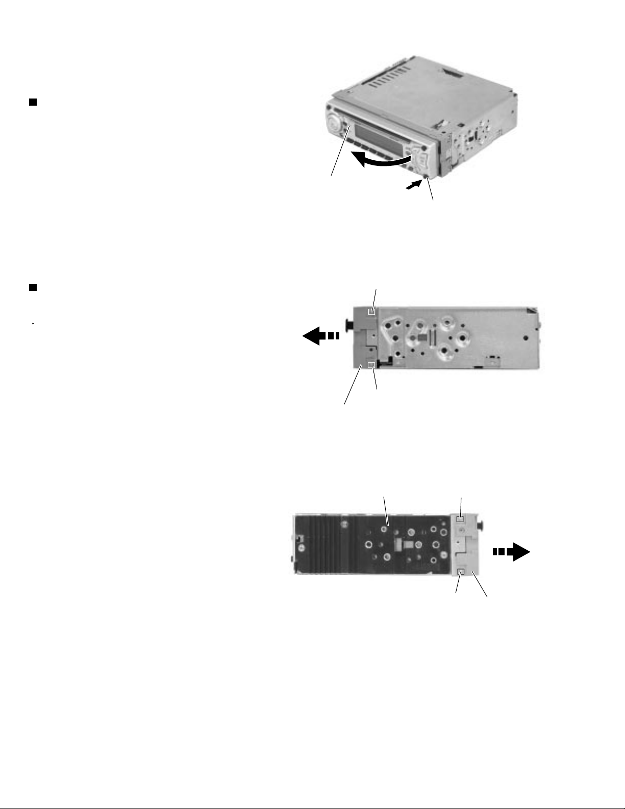
Removing the front panel assembly
(See Fig.1)
1.
Press the eject button in the lower right part of the
front panel. Remove the front panel assembly from
the body.
Front panel assembly
Eject button
Fig.1
Removing the front chassis assembly
(See Fig.2 and 3)
Prior to performing the following procedure, remove
the front panel assembly.
1.
Release the four joint tabs a on both sides of the
front chassis assembly and remove the front chassis
assembly toward the front.
Tab a
Tab a
Front chassis assembly
Heat sink
Fig.2
Tab a
1-4
Fig.3
Tab a
Front chassis
assembly
Page 5
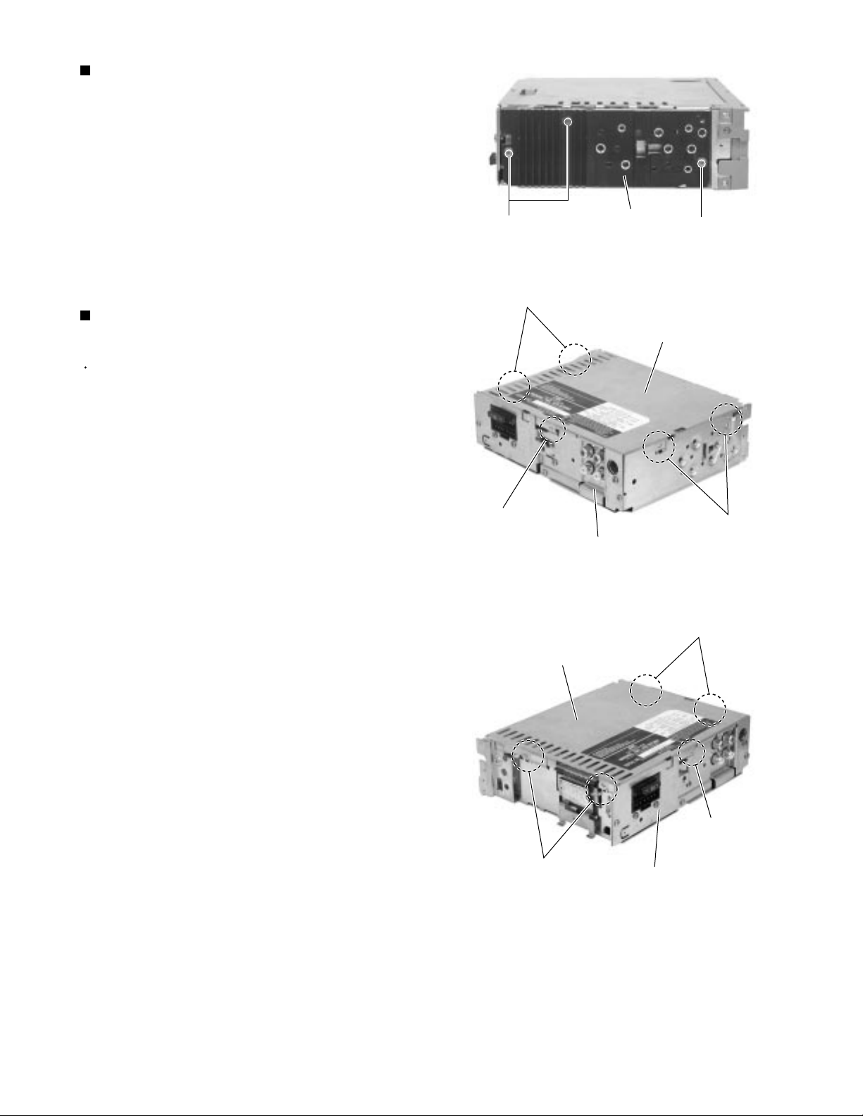
Removing the heat sink (See Fig.4)
1.
Remove the three screws A on the left side of the
body.
KD-S700GN/KD-S700BU
KD-S7250
Removing the bottom cover
(See Fig.5 and 6)
Prior to performing the following procedure, remove
the front panel assembly, the front chassis assembly
and the heat sink.
1.
Turn over the body and unjoint the five joints b with
the bottom cover and the body using a screwdriver.
A
Joints b
Joint b
Heat sink
Fig.4
Rear panel
Fig.5
A
Bottom cover
Joints b
Bottom cover
Joints b
Joints b
Joint b
Rear panel
Fig.6
1-5
Page 6
KD-S700GN/KD-S700BU
KD-S7250
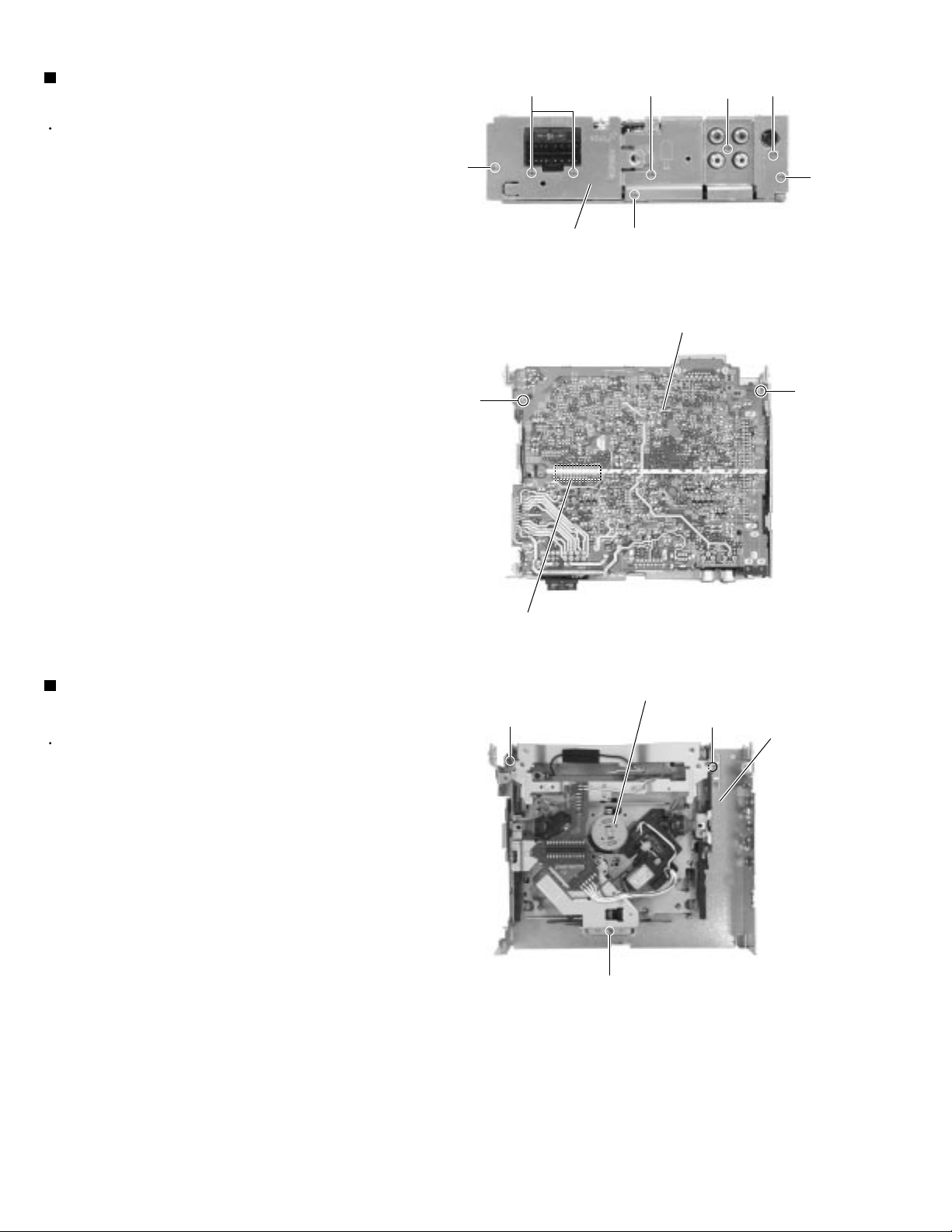
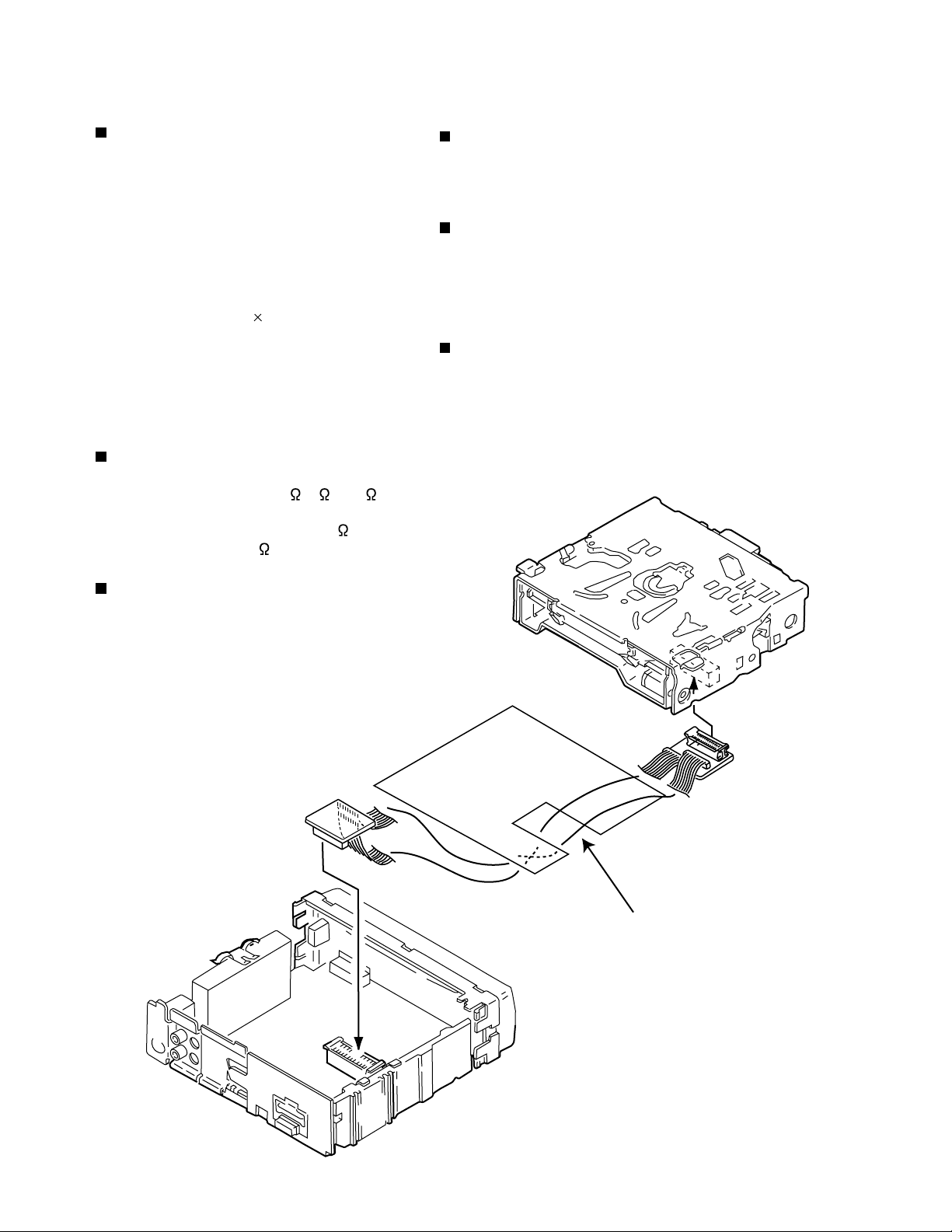
Removing the main board
(See Fig.7 and 8)
Prior to performing the following procedure, remove
the front panel assembly, the front chassis assembly,
the heat sink and the bottom cover.
1.
Remove the screw B, the four screws C and the
three screws D attaching the rear bracket on the
back of the body. Remove the rear panel.
2.
Remove the two screws E attaching the main board
on the bottom of the body. Disconnect connector
CN501 on the main board in the direction of the
arrow.
D
E
Rear panel
CC
D
Fig.7
Main board
B
C
D
E
Removing the CD mechanism section
(See Fig.9)
Prior to performing the following procedure, remove
the front panel assembly, the front chassis assembly,
the heat sink, the bottom cover and the main board.
1.
Remove the three screws F attaching the CD
mechanism section on the back of the top chassis.
CN501
F
Fig.8
CD mechanism section
F
Fig.9
F
Top chassis
1-6
Page 7
KD-S700GN/KD-S700BU
KD-S7250
Removing the control switch board
(See Fig.10 to 12)
Prior to performing the following procedure, remove
the front panel assembly.
1.
Remove the four screws G attaching the rear cover
on the back of the front panel assembly.
2.
Unjoint the twelve joints c with the front panel and
the rear cover.
3.
Remove the control switch board on the back of the
front panel.
Joints c
Front panel
G
G
Rear cover
Fig.10
Joints c
G
G
Joints c
Front panel
Rear cover
Joints c
Fig.11
Control switch board
Fig.12
1-7
Page 8
KD-S700GN/KD-S700BU
KD-S7250
<CD mechanism section>
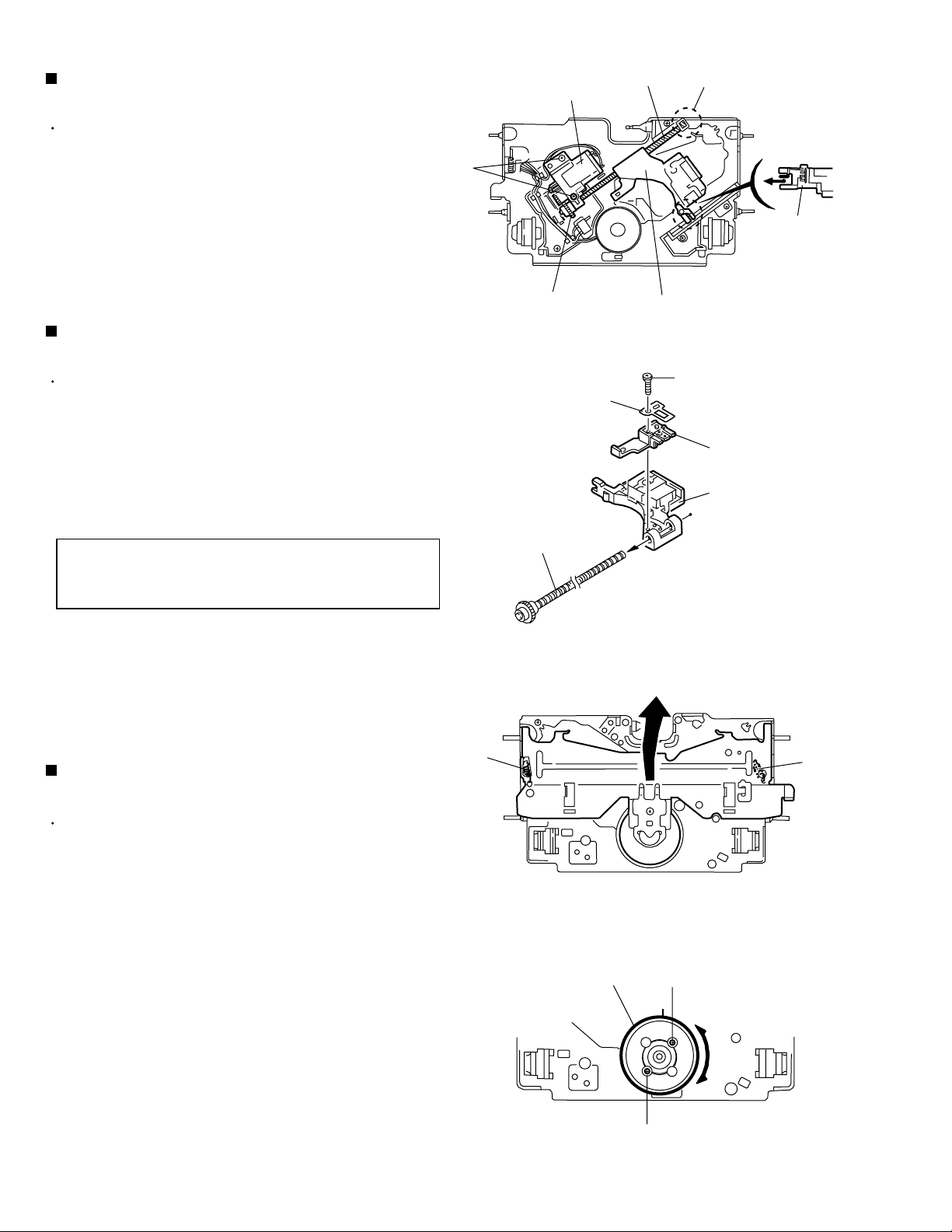
Removing the CD mechanism control
board (See Fig.1 and 2)
1.
Unsolder the part a and b on the CD mechanism
control board.
2.
Remove the stator fixing the CD mechanism control
board and the damper bracket (To remove the stator
smoothly, pick up the center part).
3.
Remove the screw A attaching the CD mechanism
control board.
4.
Remove the CD mechanism control board in the
direction of the arrow while releasing it from the two
damper bracket slots d and the front bracket slot e.
5.
Disconnect the flexible wire from connector on the
pickup unit.
ATTENTION:
Turn the FD gear in the direction of the
arrow to move the entire pickup unit to
the appropriate position where the
flexible wire of the CD mechanism unit
can be disconnected easily.
(Refer to Fig.2)
CD mechanism assembly
D
h
Front bracket
Pickup unit
Damper bracket
D
A
Fig.1
e
b
Flexible wire
a
h
c
D
d
CD mechanism
control board
Shift the lock
Removing the loading motor
(See Fig.3 to 5)
Prior to performing the following procedure, remove
the CD mechanism control board.
1.
Remove the two springs f attaching the CD
mechanism assembly and the front bracket.
2.
Remove the two screws B and the front bracket
while pulling the flame outward.
3.
Remove the belt and the screw C from the loading
motor.
Loading motor
C
FD gear
f
B
Loading motor
Pull outward
Fig.2
CD mechanism control board
f
B
Front bracket
Fig.3
Front bracket
Pull outward
1-8
Fig.5
Belt
Flame
Fig.4
Page 9
KD-S700GN/KD-S700BU
KD-S7250
Removing the CD mechanism assembly
(See Fig.1, 6 to 9)
Prior to performing the following procedure, remove
the CD mechanism control board and the front
bracket (loading motor).
1.
Remove the three screws D and the damper
bracket.
2.
Raise the both sides fix arms and move the fix plates
in the direction of the arrow to place the four shafts g
as shown in Fig.8 and 9.
3.
Remove the CD mechanism assembly and the two
springs h attaching the flame.
4.
Remove the two screws E and both sides rear
damper brackets from the dampers. Detach the CD
mechanism assembly from the left side to the right
side.
ATTENTION:
The CD mechanism assembly can be
removed if only the rear damper
bracket on the left side is removed.
CD mechanism
h
Front bracket
CD mechanism
D
Flame
assembly
D
assembly
h
D
Damper bracket
D
A
Fig.5
e
b
Damper bracket
D
Fig.6
a
h
c
D
d
CD mechanism
control board
h
Fix plate (L)
g
Fix arm (R)
D
Fig.7
Rear damper bracket
g
Fig.8
Rear damper bracket
E
Fix plate(R)
E
Fix arm (L)
Damper
Damper
g
g
Fig.9
1-9
Page 10
KD-S700GN/KD-S700BU
KD-S7250
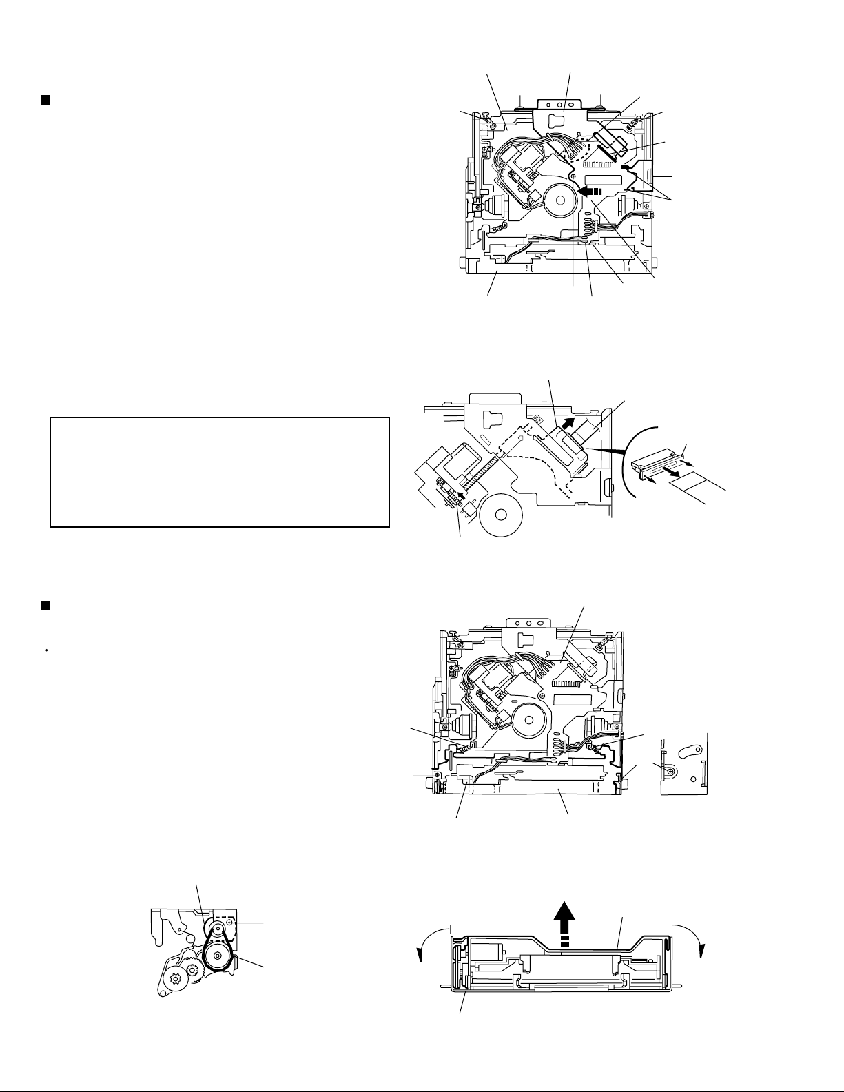
Removing the feed motor assembly
(See Fig.10)
Prior to performing the following procedure, remove
the CD mechanism control board, the front bracket
(loading motor) and the CD mechanism assembly.
1.
Remove the two screws F and the feed motor
assembly.
Removing the pickup unit
(See Fig.10 and 11)
Prior to performing the following procedure, remove
the CD mechanism control board, the front bracket
(loading motor), the CD mechanism assembly and
the feed motor assembly.
1.
Detach the FD gear part of the pickup unit upward.
Then remove the pickup unit while pulling out the
part i of the FD screw.
Feed motor assembly
F
FD gear
Nut push spring plate
FD screw
Pickup unit
Fig.10
Part i
Part j
Pickup unit
G
Pickup mount nut
Pickup unit
ATTENTION:
2.
Remove the screw G attaching the nut push spring
plate and the pickup mount nut from the pickup unit.
Pull out the FD screw.
When reattaching the pickup unit,
reattach the part j of the pickup unit,
then the part i of the FD screw.
Removing the spindle motor
(See Fig.12 and 13)
Prior to performing the following procedure, remove
the CD mechanism control board, the front bracket
(loading motor), the CD mechanism assembly and
the feed motor assembly.
1.
Turn up the CD mechanism assembly and remove
the two springs k on both sides of the clamper arms.
Open the clamper arm upward.
2.
Turn the turn table, and remove the two screws H
and the spindle motor.
k
FD screw
Spindle motor
Fig.11
k
Fig.12
H
1-10
H
Fig.13
Page 11
Adjustment method
KD-S700GN/KD-S700BU
KD-S7250
Test instruments required for adjustment
1. Digital oscilloscope (100MHz)
2. AM Standard signal generator
3. FM Standard signal generator
4. Stereo modulator
5. Electric voltmeter
6. Digital tester
7. Tracking offset meter
8. Test Disc JVC :CTS-1000
9. Extension cable for check
EXTGS004-26P 1
Standard measuring conditions
Power supply voltage: DC14.4V(11V~16V allowance)
Load impedance: 4 (4 to 8 allowance)
Line-out Level/impeadance:
2.0V/20k load(full scale)
Output Impedance: 1k
Standard volume position
Balance and Bass &Treble volume : lndication"0"
Loudness : OFF
BBE : NO BBE
Frequency Band
FM 87.5MHz ~ 107.9MHz
AM 530kHz ~ 1710 kHz
Dummy load
Exclusive dummy load should be used for AM,and FM. For
FM dummy load,there is a loss of 6dB between SSG output
and antenna input.The loss of 6dB need not be considered
since direct reading of figures are applied in this working
standard.
How to connect the extension cable for adjusting
EXTGS004-26P
1-11
Page 12

KD-S700GN/KD-S700BU
KD-S7250
Flow of functional operation until TOC read
Power ON
• When the pickup correctly moves
to the inner area of the disc
Set Function to CD
• When the laser diode correctly
emits
Microprocessor
commands
FMO
TC9490FA "40"
FEED MOTOR
+TERMINAL
TERMINAL
IC561 "6"
REST SW
• When correctly focused
FEO
TA2147F
Focus Servo Loop ON
3.3v
Pickup feeds to the inner area
1.6V
RF signal eye-pattern
remains closed
RF signal eye-pattern
opens
Disc inserted
YES
Laser emitted
Focus search
Disc rotates
Tracking loop closed
TOC readout
YES
Microprocessor
commands
TC9490FA
"38"
"1"
"No disc"
display
• When the disc correctly rotates
Microprocessor
commands
"41"
Spindle
motor (-)
IC561 "4"
AccelerationAcceleration
0.5 Sec
Rough
Servo
0.5 Sec
Servo CLV
3.3V
1.6V
1-12
Jump to the first track
Play
Tracking Servo Loop ON
• RF signal
Rough Servo Mode
CLV Servo Mode
(ProgramArea)
CLV Servo Mode
(Lead-In Area;
Digital: 0)
Page 13

Feed Section
Is the voltage output at
IC521 pin "40" 3.3V or 0V?
YES
Is 4V present at both
sides of the feed motor?
YES
NO
Is the wiring for IC521
(57) ~ (63) correct?
NO
Is 6V or 2V present at
IC561 "6" and "7"?
NO
YES
YES
Is 3.3V present at
IC561 pin "20"?
YES
Check the vicinity of
IC521.
Check the feed motor
connection wiring.
KD-S700GN/KD-S700BU
KD-S7250
NONO
Check CD 9V
and 5V.
Check the feed motor.
Focus Section
When the lens is
moving:
Does the S-search
waveform appear at
IC561 pins "8" and "9"?
Spindle Section
Is the disk rotated?
YES
Does the RF signal
appear at TP1?
YES
4V
Check IC561.
NO
YES
NO
NO
Check the circuits in
the vicinity of IC561
pins "15" ~ "18".
Check the pickup and
its connections.
Is 4V present at IC561
pins "4" and "5" ?
Check the spindle motor
and its wiring.
YES
YES
NO NO
Is 3.3V present at
IC521 pin "41" ?
YES
Check the vicinity of
IC581.
Check IC501 and
IC521.
Is the RF waveform at TP1
normal?
YES
Proceed to the Tracking
section
Tracking Section
When the disc is rotated
at first:
Is the tracking error signal
output at IC501 "11"?
Check IC521.
NO
Approx. 0.8 V
YES
Check the circuits in the
vicinity of IC501 "2" ~ "7"
"18" ~ "23"or the pickup
Check the circuit in the
vicinity of IC501 pins
"2" ~ "7","10","11
YESYES
Check the pickup and
its connections.
1-13
Page 14

KD-S700GN/KD-S700BU
KD-S7250
Maintenance of laser pickup
(1) Cleaning the pick up lens
Before you replace the pick up, please try to
clean the lens with a alcohol soaked cotton
swab.
(2) Life of the laser diode
When the life of the laser diode has expired,
the following symptoms will appear.
(1) The level of RF output (EFM output:ampli
tude of eye pattern) will be low.
Normal
1.3 0.35Vp-p?
YES
O.K
(3) Semi-fixed resistor on the APC PC board
The semi-fixed resistor on the APC printed
circuit board which is attached to the pickup
is used to adjust the laser power.Since this
adjustment should be performed to match the
characteristics of the whole optical block,
do not touch the semi-fixed resistor.
If the laser power is lower than the specified
value,the laser diode is almost worn out, and
the laser pickup should be replaced.
If the semi-fixed resistor is adjusted while
the pickup is functioning normally,the laser
pickup may be damaged due to excessive current.
NO
Replace it.
Replacement of laser pickup
Turn off the power switch and,disconnect the
power cord from the ac outlet.
Replace the pickup with a normal one.(Refer
to "Pickup Removal" on the previous page)
Plug the power cord in,and turn the power on.
At this time,check that the laser emits for
about 3seconds and the objective lens moves
up and down.
Note: Do not observe the laser beam directly.
1-14
Play a disc.
Check the eye-pattern at TP1.
Finish.
Page 15

Description of major ICs
HA13164A(IC901):Regulator
1.Terminal layout
1 2 3 4 5 6 7 8 9 101112131415
KD-S700GN/KD-S700BU
KD-S7250
2.Block diagram
ANT OUT
C3
0.1u
EXT OUT
C4
0.1u
ANT CTRL
CTRL
CD OUT
C5
0.1u
AUDIO OUT
C6
10u
11
12
10
BATT.DET OUT
9
COMPOUT
6
VDD OUT
4
SW5VOUT
5
14
UNIT R:
+B
ACC
ILMOUT
R1
C7
0.1u
C8
0.1u
C1
100u
VCC ACC
8
2
1
7
Surge Protector
BIAS TSD
15
3
TA B
note1) TAB (header of IC)
connected to GND
ILM AJGND GND
13
C2
0.1u
C:F
3.Pin function
Pin No. Symbol Function
1
2
EXTOUT
ANTOUT
Output voltage is VCC-1 V when M or H level applied to CTRL pin.
Output voltage is VCC-1 V when M or H level to CTRL pin and H level
to ANT-CTRL.
3
4
5
6
7
8
9
10
11
12
13
14
15
ACCIN
VDDOUT
SW5VOUT
COMPOUT
ANT CTRL
VCC
BATT DET
AUDIO OUT
CTRL
CD OUT
ILM AJ
ILM OUT
GND
Connected to ACC.
Regular 5.7V.
Output voltage is 5V when M or H level applied to CTRL pin.
Output for ACC detector.
L:ANT output OFF , H:ANT output ON
Connected to VCC.
Low battery detect.
Output voltage is 9V when M or H level applied to CTRL pin.
L:BIAS OFF, M:BIAS ON, H:CD ON
Output voltage is 8V when H level applied to CTRL pin.
Adjustment pin for ILM output voltage.
Output voltage is 10V when M or H level applied to CTRL pin.
Connected to GND.
1-15
Page 16

KD-S700GN/KD-S700BU
KD-S7250
UPD178078GF-559 (IC701) : System CPU
81
~
BUSINT
BUSSI
BUSSO
JBUS-SCK
VOL-DA
VOL-CLK
LCDDA
LCDCLK
BUSI/O
LCDCE
SW2
SW3
SW4
RSTSW
ENC1
ENC2
KEY0
KEY1
KEY2
LEVEL
AVDD
SM
AVSS
REGCPU
VDD
REGOSC
X2
X1
GND0
SD/ST
GND2
IFC
VDDPLL
OSC
80 ~ 51
50
~
31
1 ~ 30
1.Pin layout
100
2.Pin function (1/2)
Pin
NO.
1
2
3
4
5
6,7,8
9
10
11
12
13
14
15
16
17
18
19
20
21
22
23
24
25
26
27
28
29
30,31
32
33
34
35
36
37
38
39
40
41
42
43
44
45
I/OSymbol FUNCTION
-
No use
I
JVC bus communication line
I
JVC bus communication line
O
JVC bus communication line
O
JVC bus communication line
-
No use
O
Serial data for volume
O
Serial clock for volume
-
No use
O
LCD driver serial data output
O
Serial data for LCD
O
JVC bus output select
-
No use
O
LCD driver communication line
I
CD mech switch
I
CD mech switch
I
CD mech switch
I
Traverse mech rest switch
I
Encoder input
I
Encoder input
I
Key input
I
Key input
I
Key input
I
Audio level input
-
Power supply
I
Signal level meter input
-
No use
-
No use
-
Connect to GND
-
Connect to GND with capacitor
-
Power supply
-
Connect to GND don't have tap
-
System clock
I
System clock
-
Connect to GND
I
Station detector & Stereo indicator
-
Connect to GND
-
No use
I
IF count input
-
---
I
FM,AM osc input
-
No use
1-16
Page 17

KD-S700GN/KD-S700BU
KD-S7250
2.Pin function (2/2)
Pin
NO.
46
GNDPLL
47
AMEO
48
FMEO
49
IC(VPP)
50
RESET
51
SW1
52
REMOCON
53
VTR-LOGIC
54
VR-CONT
55
POWER
56
CDON
57
MUTE
58
STAGE
59
BUZZER
60
JAPAN
61~67
68
CDRW
69
LM0
70
LM1
71
BUCK
72
CCE
73
BUS0
74
BUS1
75
BUS2
76
BUS3
77
RST
78
PS1
79
PS2
80
DETACH
81
82
GND1
83
MONO
84
SEEK/STOP
85
FM/AM
86
87
ANT
88
TEL MUTE
89~98
100
99
NC
VDDPORT
GNDPORT
I/OSymbol FUNCTION
-
---
O
PLL error output for AM
O
PLL error output for FM
-
Setting to write for flash
I
System reset
I
CD mech switch
I
Remocon input
-
No use
-
No use
O
Power control
O
CD power control
O
Mute control
-
No use
-
No use
-
No use
-
No use
O
CD-RW detect signal output
O
CD mech driver control
O
CD mech driver control
O
CD LSI communication line
O
CD LSI communication line
I/O
I/O
I/O
I/O
CD LSI communication line
CD LSI communication line
CD LSI communication line
CD LSI communication line
O
CD LSI communication line
I
ACC detection input
I
Memory detection
I
Detach detection
-
No use
-
Connect to GND
O
Mono by force
O
Switching SEEK & STOP
O
Band switch
-
No use
O
Antena regulator control signal
-
No use
-
Non connection
-
Vdd
-
Connect to GND
UPD178078GF-559
1-17
Page 18

KD-S700GN/KD-S700BU
KD-S7250
TA2147F-X(IC501):RF AMP
1.Terminal layout
2.Block diagram
VRO
FEO
FEN
RFRP
RFRPIN
RFGO
RFGC
AGCIN
RFO
RFN
13GVSW
14
15
16
17
18
19
20
21
22
23
10pF
40k
30k
20k 20k
20k
20k
BOTTOM
3k
15k
50 A
12k
12k
PEAK
20k
180k
40pF
20k
20k
PEAK
1.3V
180k
40k
240k
15pF
240k
15pF
60k
40k
40pF
60k
50k
2k
20 A
20k
60 A
50k
14k
k
1
80k
x0.5
x0.5
80k
20k
20k
15k
x2
x2
1k
2k
1.75k
10pF
12 RFDC
11
TEO
10
TEN
TEBC
9
8
SEL
7
LDO
MDI
6
5
TNI
4
TPI
3
FPI
2
FNI
1-18
GND
24
3k
1
Vcc
Page 19

KD-S700GN/KD-S700BU
KD-S7250
3.Pin function
Pin No.
1
2
3
4
5
6
7
8
9
10
11
12
13
Symbol
Vcc
FNI
FPI
TPI
TNI
MDI
LDO
SEL
TEBC
TEN
TEO
RFDC
GVSW
I/O
Function
-
3.3V Power supply pin
I
Main-beam amp input pin
I
Main-beam amp input pin
I
Sub-beam amp input pin
I
Sub-beam input pin
I
Monitor photo diode amp input pin
O
Laser diode amp output pin
I
APC circuit ON/OFF control signal,laser diode (LDO) control signal input or
bottom/peak detection frequency change pin.
APC
circuit
GND OFF
HIZ
Vcc
I
Tracking error balance adjustment signal pin
Adjusts TE signal balance by eliminating carrier component from
PWM signal(3-state output, PWM carrier = 88.2kHz) output from
TC9490F/FA TEBC pin using RC-LPF and inputting DC.
TEBC input voltage:GND~Vcc
I
Tracking error signal generation amp negative-phase input pin
O
Tracking error signal generation amp output pin.
Combining TEO signal and RFRP signal with TC9490F/FA configures
tracking search system.
O
RF signal peak detection output pin
I
AGC/FE/TE amp gain change pin
Connected to Vcc
through 1k resistor
Control signal output
ON
Control signal output
ON
LDOSEL
TA2147F-X
14
15
16
17
18
19
20
21
22
23
24
VRO
FEO
FEN
RFRP
RFRPIN
RFGO
RFGC
AGCIN
RFO
RFN
GND
ModeGVSW
GND
HIZ
Vcc
Reference voltage (VRO) output pin *VRO = 1/2 Vcc when Vcc = 3.3V
O
Focus error signal generation amp output pin
O
Focus error signal generation amp negative-phase input pin
I
Signal amp output pin for track count
O
Combining RFRP signal TEO signal with TC9490F/FA configures tracking
search system.
Signal generation amp input pin for track count
I
RF signal amplitude adjustment amp output pin
O
RF amplitude adjustment control signal input pin
I
Adjusts RF signal amplitude by eliminating carrier component from PWM
signal (3-state output, PWM carrier = 88.2kHz) output from TC9490F/FA
RFGC pin using RC-LPF and inputting DC.
*RFGC input voltage : GND-Vcc
RF signal amplitude adjustment amp input pin
I
RF signal generation amp output pin
O
RF signal generation amp input pin
I
GND pin
-
CD-RW
CD-DA
CD-DA
1-19
Page 20

KD-S700GN/KD-S700BU
/
KD-S7250
TC9490FA(IC521):DSP&DAC
1.Terminal layout & block daiagram
DV
SS3
RO
DV
DD3
DVR
LO
DV
SS3
ZDET
V
SS5
BUS0
BUS1
BUS2
BUS3
BUCK
/CCE
/RST
VXDD3XOXI
SS3
XV
TEIN
DD3VSS3
V
DMO
FMO
DD3
AV
SEL
TEBC
RFGC
48 47 46 45 44 43 42 41 40 39 38 37 36 35 34 33
49
50
51
52
LPF
Clock
generator
1-bit
DAC
PWM
Servo control
A/D
53
54
55
56
Address
circuit
ROM
RAM
Digital equalizer
automatic
adjustment circuit
57
58
59
60
61
62
Micro-
controller
interface
circuit
Correction
Audio output
circuit
16k
RAM
Digital output
CLV servo
Sync signal
protection
EFM
Sub code
detector
TMAX
63
VCO
PLL
REF
V
D/A
Data
slicer
TRO
FOO
32
31
30
29
28
27
26
25
24
23
22
21
20
19
18
TEZI
TEI
SBAD
FEI
RFRP
RFZI
RFCT
AV
DD3
RFI
SLCO
AV
SS3
VCOF
RV
REF
LPFO
LPFN
1-20
64
V
DD5
17
TMAX
1 2 3 4 5 6 7 8 9 10 11 12 13 14 15 16
BCK
LRCK
AOUT
DOUT
IPF
DD3
V
V
SBOK
CLCK
DATA
SFSY
SBSY
/HSO
UHSO
DD3
PV
PDO
SS3
Page 21

KD-S700GN/KD-S700BU
KD-S7250
2.Pin function
Pin No.
1
2
3
4
5
6
7
8
9
10
11
12
13
14
Symbol
BCK
LRCK
AOUT
DOUT
IPF
VDD3
VSS3
SBOK
CLCK
DATA
SFSY
SBSY
/HSO
/UHSO
I/O
Function
O
Bit clock outputpin 32fs, 48fs, or 64fs selectable by command.
O
L/R channel clock output pin."L" for L channe and "H" for R channel.
Output polarity can be inverted by command.
O
Audio data output pin. MSB-first or LSB-first selectable by command.
O
Digital data output pin. Outputs up to double-speed playback.
O
Correction flag output pin.When set to "H",AOUT output cannot be corrected
by C2 correction processing.
-
Digital 3.3V power supply voltage pin.
-
Digital GND pin.
O
Subcode Q data CRCC result output pin."H" level when result is OK.
I/O
Subcode P-W data read clockI/O pin. I/O polarity selectable by command.
O
Subcode P-W data output pin.
O
Playback frame sync signal output pin.
O
Subcode block sync signal output pin. "H" level at S1 when subcode sync is
detected.
O
Playback speed mode flag output pins.
/HSO
Playback speed/UHSO
O
H
H
L
--
H
L
L
--
Normal
Double
4 times
---
TC9490FA(2/3)
15
16
17
18
19
20
21
22
23
24
25
26
27
28
29
30
31
32
33
34
35
PVDD3
PDO
TMAX
LPFN
LPFO
PVREF
VCOF
SS3
AV
SLCO
RFI
AV
RFCT
RFZI
RFRP
FEI
SBAD
TEI
TEZI
FOO
TRO
REF
V
-
PLL-only 3.3V power supply voltage pin.
O
EFM and PLCK phase difference signal output pin.
O
TMAX detection result output pin.
TMAX OutputTMAX Detection result
Longer than fixed period
Within fixed period
Shorter than fixed period
I
Inverted input pin for PLL LPF amp.
O
Output oin for PLL LPF amp.
REF
-
PLL-only V
VCO filter pin.
O
Analog GND pin.
DAC output pin for data slice level generation.
O
RF signal input pin.Zin selectable by command.
I
Analog 3.3V power supply voltage pin.
RFRP signal center level input pin.
I
RFRP signal zero-cross input pin.
I
RF ripple signal input pin.
I
Focus error signal input pin.
I
Sub-beam adder signal input pin.
I
Tracking error input pin. Inputs when tracking servo is on.
I
Tracking error signal zero-cross input pin.
I
Focus equalizer output pin.
O
Tracking equalizer output pin.
O
Analog reference power supply voltage pin.
-
pin.
"PV
"HIZ"
"AV
DD3
SS3"
"
1-21
Page 22

KD-S700GN/KD-S700BU
KD-S7250
2.Pin function
Pin No.
36
37
38
39
40
41
42
43
44
45
46
47
48
49
50
51
52
53
54
55
56
57
58
59
60
61
62
63
64
Symbol
RFGC
TEBC
SEL
AV
DD3
FMO
DMO
V
SS3
V
DD3
TESIN
XV
SS3
XI
XO
XV
DD3
DV
SS3
RO
DV
DD3
DVR
LO
DV
SS3
ZDET
V
SS5
BUS0
BUS1
BUS2
BUS3
BUCK
/CCE
/RST
V
DD5
I/O
O
O
O
O
O
-
-
I
-
I
O
-
O
-
O
O
-
I/O
I
I
I
-
TC9490FA(3/3)
Function
RF amplitude adjustment control signal output pin.
Tracking balance control signal output pin.
APC circuit ON/OFF signal output pin. At laser on,high impedance with
UHS="L" ,H output with UHS="H".
Analog 3.3V power supply voltage pin.
Feed equalizer output pin.
Disc equalizer output pin.
Digital GND pin.
Digital 3.3V power supply voltage pin.
Test input pin. Normally,fixed to "L".
System clock oscillator GND pin.
System clock oscilatoe input pin.
System clock oscillator output pin.
System clock oscillator 3.3V power supply voltage pin.
DA converter GND pin.
R-channel data forward output pin.
DA converter 3.3V power supply pin.
Reference voltage pin.
L-channel data forward output pin.
DA converter GND pin.
1 bit DA converter zero data detection flag output pin.
Microcontroller interface GND pin.
Microcontroller interface data I/O pins.
Microcontroller interface clock input pin.
Microcontroller interface chip enable signal input pin.At "L".
Bus0 to BUS3 are active.
Reset signal input pin. At reset,"L".
Microcontroller interface 5V power supply pin.
1-22
Page 23

BD3860K (IC161):E.Vol&LOUD
1.Terminal layout
33 23
KD-S700GN/KD-S700BU
KD-S7250
2.Block diagram
GND FIL VCC SEL1
6 5 9 40 36 35 343328323130 2919 15 14
POWER
SUPPLY
A1
41
B1
42
C1
43
D1
44
INPUT
1
2
3
4
SELECTOR
A2
B2
C2
D2
34
44
1 11
INPUT
GAIN
0 18 dB
INPUT
GAIN
0 18 dB
22
12
VIN1 LOUD1 HF1 LF1 DET1 TIN1 TNF1 BNF1
MAIN
VOLUME
0 -40 dB
LOUDNESS
MAIN
VOLUME
0 -40 dB
LOUDNESS
LOW(f=50Hz) 6dB
PROCESS CONTROL +3 to 12dB
(f=10kHz)
LOGIC
LOW(f=50Hz) 6dB
PROCESS CONTROL +3 to 12dB
(f=10kHz)
TREBLE
-14 +14dB
TREBLE
-14 +14dB
-14 +14dB
-14 +14dB
BASS
BASS
BOUT1VCA1 MIX1 BBOUT1
FADER
CH1 FRONT
0 -5 dB
FADER
CH1 REAR
0 -5 dB
FADER
CH2 REAR
0 -5 dB
FADER
CH2 FRONT
0 -5 dB
OUTF1
13
OUTR1
12
SI
7
8
SC
37
OUTR2
10
OUTF2
11
3.Pin function
Pin
Symbol Function
No.
1
2
3
4
5
6
7
8
9
10
11
12
13
14
15
16
17
18
19
20
21
22
A2
B2
C2
D2
FIL
GND
SI
SC
VCC
OUTR2
OUTF2
OUTR1
OUTF1
BOUT1
BNF1
BOUT2
BNF2
TNF2
TNF1
TIN2
BBOUT2
MIX2
CH2 Input Pin A
CH2 Input Pin B
CH2 Input Pin C
CH2 Input Pin D
1/2 VCC Pin
Ground Pin
Serial Data Receiving Pin
Serial Clock Receiving Pin
Power Supply Pin
CH2 Rear Output Pin
CH2 Front Output Pin
CH1 Rear Output Pin
CH1 Front Output Pin
CH1 Bass Filter Setting Pin
CH1 Bass Filter Setting Pin
CH2 Bass Filter Setting Pin
CH2 Bass Filter Setting Pin
CH2 Treble Filter Setting Pin
CH1 Treble Filter Setting Pin
CH2 Treble Input Pin
CH2 BBE II Signal Output Pin
CH2 Output MIX Amplifier
Inverse Input Pin
39 38 37 25 24 26 23 22 21 20 18 17 16
Pin
Symbol Function
No.
23
24
25
26
27
28
29
30
BBOUT1
31
32
33
34
35
36
37
38
39
40
41
42
43
44
VCA2
LF2
HF2
DET2
DEF
DET1
TIN1
MIX1
VCA1
LF1
HF1
LOUD1
VIN1
LOUD2
VIN2
SEL2
SEL1
A1
B1
C1
D1
CH2 High Pass VCA Output Pin
CH2 Low Pass Filter Setting Pin
CH2 High Pass Filter Setting Pin
CH2 High Pass Attack/Release Time Setting Pin
BBE ON/OFF switching time constant pin
CH1 High Pass Attack/Release Time Setting Pin
CH1 treble Input Pin
CH1 BBE II Signal Output Pin
CH1 Output MIX Amplifier Inverse Input Pin
CH1 High Pass VCA Output Pin
CH1 Low Pass Filter Setting Pin
CH1 High Pass Filter Setting Pin
CH1 Loudness Filter Setting Pin
CH1 Main Volume Input Pin
CH2 Loudness Filter setting Pin
CH2 Main Volume Input Pin
CH2 Input Gain Output Pin
CH1 Input Gain output Pin
CH1 Input Pin A
CH1 Input Pin B
CH1 Input Pin C
CH1 Input Pin D
BOUT2BNF2TNF2TIN2BBOUT2MIX2VCA2DET2LF2HF2LOUD2VIN2SEL2
1-23
Page 24

KD-S700GN/KD-S700BU
KD-S7250
LA4743K(IC302):Power AMP
1.Block diagram
IN 1
TA B
IN 2
+
0.22 F
+
0.22 F
11
1
12
Vcc 1/2 Vcc 3/4
6 20
-
+
Protective
circuit
-
+
2200 F 0.022 F
+
9
7
+
OUT 1+
OUT 1-
PWR GND1
8
+
OUT 2+
5
-
OUT 2-
3
PWR GND2
2
ST BY
R.F
47 F
IN 3
PRE GND
IN 4
+5V
ST ON
+
0.22 F
N.C
+
0.22 F
4
Stand by
Switch
Mute
10
+
Ripple
Filter
Mute
22
circuit
3.3 F
+
15
-
+
-
17
19
10K
+
OUT 3+
OUT 3-
Low Level
Mute ON
25
18
21
23
PWR GND3
OUT 4+
OUT 4-
13
14
Protective
circuit
-
+
+
-
1-24
ON TIME C
22 F
Muting &
16
+
ON Time Control
Circuit
PWR GND4
24
Page 25

2.Terminal layout
KD-S700GN/KD-S700BU
KD-S7250
3.Pin function
1
2
3
4
5
6
7
8
9
10
11
12
13
14
15
16
17
18
19
20
21
22
23
24
25
SymbolPin No. Function
TA B
GND
RFOSTBY
RFO+
VCC1/2
RROGND
RRO+
VREF
RRIN
RFIN
SGND
LFIN
LRIN
ONTIME
LRO+
GND
LROVCC3/4
LFO+
MUTE
LFO-GND
NC
Header of IC
Power GND
Outpur(-) for front Rch
Stand by input
Output (+) for front Rch
Power input
Output (-) for rear Rch
Power GND
Output (+) for rear Rch
Ripple filter
Rear Rch input
Front Rch input
Signal GND
Front Lch input
Rear Lch input
Power on time control
Output (+) for rear Lch
Power GND
Output (-) for rear Lch
Power input
Output (+) for front
Muting control input
Output (-) for front
Power GND
No connection
LA4743K
1-25
Page 26

KD-S700GN/KD-S700BU
KD-S7250
LA6574H-X (IC561) :CD driver
1.Terminal layout & brock daiagram
VCC2 1
V05- 2
V05+ 3
V04+ 4
V04- 5
V03+ 6
V03- 7
FR FR
V02+ 8
V02- 9
V01+ 10
V01- 11
VCC1 12
VIN1 13
VIN1G 14
CH5
POWER supplise
CH5
CH4
CH3
CH2
CH1
CH1.2.3.4
POWER
11k
Thermal Shutdown
Level Shift Level Shift Level Shift Level ShiftOutput Control
22k
Input
22k 11k
Signal System Power
3.3VREG (External
PNP Tr)
22k
11k
22k
11k
28 REV
27 FWD
26 S-GND
25 VCONT
24 VIN4
23 VIN4G
22 VCC-S
FR FR
21 VREF-IN
20 REG-OUT
19 REG-IN
18 VIN3G
17 VIN3
16 VIN2G
15 VIN2
2.Pin function
Pin
No.
1
2
3
4
5
6
7
8
9
10
11
12
13
14
1-26
Symbol Function Symbol Function
VCC2
VO5VO5+
VO4+
VO4VO3+
VO3VO2+
VO2VO1+
VO1VCC1
VIN1
VIN1G
CH5 power supplies.
Loading output(-)
Loading output(+)
CH4 output terminal(+)
CH4 output terminal(-)
CH3 output terminal(+)
CH3 output terminal(-)
CH2 output terminal(+)
CH2 output terminal(-)
CH1 output terminal(+)
CH1 output terminal(-)
CH1,2,3,4 power supplies
CH1 input terminal
CH1 input terminal
Pin
No.
15
16
17
18
19
20
21
22
23
24
25
26
27
28
VIN2
VIN2G
VIN3
VIN3G
REG-IN
REG-OUT
VREF-IN
VCC-S
VIN4G
VIN4
VCONT
S-GND
FWD
REV
CH2 input terminal
CH2 input terminal(for gain adjustment)
CH3 input terminal
CH3 input terminal(for gain adjustment)
Regulator terminal
Regulator terminal
Standard voltage input terminal
Signal system power
CH4 input terminal(for gain adjustment)
CH4 input terminal
CH5 output voltage set terminal
Signal system GND
CH5 output switch terminal
CH5 output switch terminal
(for gain adjustment)
Page 27

HD74HC126FP-X (IC801) : Buffer
KD-S700GN/KD-S700BU
KD-S7250
1.Terminal layout
1C
1
1A
2
1Y
3
2C
4
2A
5
2Y
6
GND
7
2.Block diagram
Input
VU
14
4C
13
4A
12
4Y
11
3C
10
3A
9
3Y
8
Vcc Vcc
1A
2A
3A
4A
1C
2C
3C
See Function Table
4C
3.Pin function
Output
1Y
2Y
Output
2Y
Output
3Y
Output
4Y
Input
C
L
H
H
Output
A
X
L
H
Y
Z
H
L
Note) H:High level
L:Low level
X:Irrelevant
Z:Off(High-impedance)
State a 3-state input
1k
S1
CL
1k
Sample as Load Circuit 1
Sample as Load Circuit 1
Sample as Load Circuit 1
Note) CL includes probe and jig capacitance
1-27
Page 28

KD-S700GN/KD-S700BU
KD-S7250
PT6523LQ(IC601):LCD DRIVER
1.Pin layout
48 ~ 33
49
32
64
1 ~ 16
2.Block diagram
VDD1
VDD2
INH
OSC
DI
CLK
CE
VDD
VSS
17
COM1 COM2 COM3 SG52 SG5 SG4 SG3 SG2 SG1
DRIVER
CLOCK
GENERATOR
ADDRESS
DETECTOR
SEGMENT DRIVER & LATCHCOMMON
SHIFT REGISTER
3.Pin function
Pin No.
1 ~ 52
53 ~ 55
56
57
58
59
60
61
62
63
64
Pin Name I/O Description
SG1 ~ SG52
COM1 ~ COM3
VDD
O
O
Segment output pins
Common driver output pins
Power supply
Display OFF control input pin.
I
When this pin is "LOW", the display is forcibly/turned OFF.
INH
(SG1 to SG52, COM1 to COM3 are set to "LOW").
When this pin is set to "High", the display is ON.
(See Note 1*)
VDD1
Used for the 2/3 bias voltage when the bias voltages
I
are provided externally. Connect to VDD2 when 1/2 bias
is used.
VDD2
Used for 1/3 bias voltage when the bias voltages are
I
provided externally. Connect to VDD1 when 1/2 bias
used.
VSS
OSC
CE
CLK
DI
-
I/O
I
I
I
Ground pin
Oscillation Input/Output pin
Chip enable pin
Synchronization clock
Transfer data pin
*Note 1: When INH="LOW" : Serial data transfers can be performed when the display is forcibly OFF.
1-28
Page 29

NJM4565M-WE (IC571) : Ope. amp
A OUTPUT
1
KD-S700GN/KD-S700BU
KD-S7250
+
8
V
-
A INPUT
+
A INPUT
2
3
-
4
V
RPM6938-SV4(IC602) : Remote sensor
1.Block diagram
AMP
I/V
conversion
BPF
B OUTPUT
7
B INPUT
-
6
5
+
B INPUT
AGC
Detector
Vcc
Comp
Vcc
22k
Rout
PD
magnetic shield
fo
trimming
circuit
GND
1-29
Page 30

Block diagram
REST
SW
LOADING
MOTOR
FEED
MOTOR
SPINDLE
MOTOR
SW1 SW4
PICK UP
REST
LOADING
LOADING
FEED
SPINDLE
SW1 SW4
A,B,C D,E,F
LD.MD
TRACKING
FOCUS
SW1 SW4
REST
LOADING
SPINDLE
FEED
TRACKING
FOCUS
CN501
VA,VB,VC
VE,VF,MD,LD
LM0
LM1
IC561
SERVO
CD
DRIVER
IC501
RF AMP
FEED
DMO,FMO,FOD,TRO
RF-GC,RF
RFRP,TE
SEL,TEB
RFDC,TE
CD-RW
IC571
CD
LPF
LO
RO
IC151
DSP
&
DAC
CD. L
CD. R
BUS0 BUS3
BUCK,CCE
RST,CDON
CJ1
ANT
CD.L
CD.R
AMEO
FMEO
TU1
FM/AM
TUNER
FM/AM
FMOSC
IFC
AGC
S.METER
SD/ST ,MONO
S.METER
IC701
MICON
SI
SC
TU.LCH
TU.RCH
ANT
CDON
PS2
IC161
E.VOL
IC901
REGULATOR
KD-S700GN/KD-S700BU
KD-S7250
LRO
RRO
LFO
LRO
RFO
RRO
IC302
POWER
AMP
LF
RF
LR
RR
CJ302
LINE OUT
IC601 S619
KEY
MATRIX
LCD1
COM1
COM2
COM3
S50
S1
IC602
REMOCON
REMOCON
KEY0,KEY1,KEY2
IC601
LCD
DRIVER
JS690
ENCODER
LCD_CO
LCD_CLK
LCD_SO
ENC1
ENC2
CJ601
CJ961
REMOCON
ENC1
ENC2
LCD.CL
LCD.CE
LCD.DA
KEY0
KEY1
KEY2
EACH BLOCK
CN901
SPK
BATTERY
-
Page 31

l
Standard schematic diagrams
Main amp section
CJ1
QNB0100-002
C41
R42
R43
1k
3.9k
0.056
C42
0.012
Q41
2SC3661-X
R41
3.3V
FEED+
FEED-
REST
CD.L
A-GND
CD.R
BUS0
BUS1
BUS2
BUS3
BUCK
CCE
RST
SW5V
CDON
CD-RW
CD8V
1k
9V
LM0
LM1
SW1
SW2
SW3
SW4
DETACH
ILL_10V
R5V
REMOCON
ENC1
ENC2
LCD.CL
LCD.DA
LCD.CE
KEY0
KEY1
KEY2
CJ691
VMC0334-001
C710
0.1
C711
1000p
D701
UDZS6.2B-X
UDZS6.2B-X
D702
UDZS6.2B-X
D703
D704
UDZS6.2B-X
D705
UDZS6.2B-X
UDZS6.2B-X
D706
D707
UDZS6.2B-X
D708
UDZS6.2B-X
D709
UDZS6.2B-X
Q42
2SC3661-X
C31
2.2/50
R32
R33
1k
0.001
2SD601
AMEO
FMEO
ANT
TELMUTE
10k
C33
BZ841
220/10
DETACH
R747
MONO
SEEK/STP
FM/AM
JBUS.INT
JBUS.SI
JBUS.SO
JBUS.SCK
JBUS.I/O
QAN0009-001Z
2.2k
R841
Q841
UN2211-X
Q32
C32
Q31
1.5k
2SD601
R31
5p
C5
R34
470
D31
MTZJ10C-T1
10k
VDD
VSS
KD-S700GN/KD-S700BU
KD-S7250
1SS133
TU1
QAU0257-001
L1
4.7u
1k
R3
1k
R1
10k
R10
10
10/16
0.022
C22
R27
Q22
2SB709
D21
1SS133
R24
2.2k
ILL_10V
10k
R748
R750
R976
R701
R702
R703
C841
0.1/50
Q2
C21
Q21
2SB1197
R23
10k
D22
1SS133
R22
1k
Q23
UN2211-X
C35
47p
PS2
RST
10k
0
47k
R749
R746
47k
4.7k
4.7k
4.7k
R704
R710
R711
R712
R713
R686
R685
BUZZER
R842
1k
C912
150p
UN2211-X
R21
FM/AM
BUS3
47k
47k
47k
47k
47k
47k
47k
4.7/25
BUS2
10/16
1SS133
1SS133
D1
D2C1C18
10k
15
15
R26
R25
9V
LM1
CCE
BUCK
BUS0
BUS1
2.2k
R745
SC
SI
0.1/50
C3
220/16
C24
LM0
CD-RW
LM1
2.2k
R744
IC701
UPD178078GF-559
2.2k
2.2k
R708
R707
R706
LCD.CL
LCD.DA
47
15p
0.033
0.033
0.22/50
C2
R2
C83
C16
R9
8.2k
0.01
R8
C85
22k
FM.OSC
LM0
2.2k
0
R709
LCD.CE
S.METER
R5V
BUZZER
47k
R739
10k
10k
R714
R715
SW4
SW3
SW2
ENC2
ENC1
REST
C84
FEED+
0.01
C14
IF.C
MUTE.CONT
CDON
FEED-
10k
R5
SEEK/STP
POWER
D971
ISS355
ISS355
SD/ST
REMOCON
R735
R721
R719
R717
S.METER
D972
47k
R4
Q1
UN2211-X
SW1
10k
MONO
10k
10k
10k
KEY0
0.1/50
C12
C17
2.7k
2.7k
R81
R82
1/50
4.3k
4.3k
1/50
R83
C82
C81
R84
56p
TU.LCH
VDD
TU.RCH
VPP
R731
R729
R727
R726
R724
47k
R723
47k
R722
4.7k
R720
4.7k
R718
4.7k
KEY2
KEY1
R971
47k
MUTE.CONT
JBUS.INT
JBUS.SCK
JBUS.I/O
JBUS.SO
JBUS.SI
R734
100k
RESET
FMEO
AMEO
47k
0.01
C708
FM.OSC
IF.C
47k
0
SD/ST
0
QAX0406-001Z
R716
10k
VDD
9V
Q971
2SD601
KD-S700GN/KD-S700BU
KD-S7250
Q976
47/6.3
C976
C705
220/10
UN2111
Q977
0.082
C975
100k
0.01
C801
R811
R803
0
C709
0.1
C706
22p
22p
C702
0.1
C701
UN2111
UDZ11B-X
C977
D977
100/16
R808
R809
R810
10k
R802
100k
C162
470p
CD.L
TU.LCH
CH.LCH
CD.R
TU.RCH
CH.RCH
SI
SC
R244
4.7u
L702
R5V
ANT
POWER
CDON
CD8V
ILL-10V
PS2
22k
330
10047k
R804
R805
R801
100k
R172
R162
6.8k
6.8k
C173
C163
0.1
0.1
C172
R171
470p
220k
R161
220k
C161
10/16
C171
10/16
C597
10/16
C803
10/16
C587
10/16
C802
10/16
R242
R241
R175
2.2k
R176
2.2k
R246
R245
180k
12k
Q241
2SD601
C243
0.047
D242
R248
100
1SS133
56k
22/16
C244
D243
C242
0.22/50
1SS133
1k
R906
1.2k
R905
D976
C333
0.047
47k
R733
R732
10k
C707
220/10
R728
47k
X1
X701
0.1
C703
R725
47k
L701
4.7u
C211
0.01
R243
1k
R806
47k
R807
100
HD74HC126FP
IC801
C212
0.1
220k
220k
D244 D245
1SS133
22k
R249
R247
1001k
LFO
MUTE
D331
1SS133
D341
1SS133
1M
1M
0.0047
R201
4.7/25
4.7/25
C202
0.1
R211
C213
C205
C215
470p
R221
C214
0R0
C174
C201
0.01
10/16
IC161
BD3860K
47/16
C178
C180
1SS133
C245
1/50
47k
B962
R961
0
51k
Q964
UN2211
100/16
2SB709
Q963
TELMUTE
0.1
C216
C181
C182
C179
R335
R325
R321
RFO
R351
LRO
R355
R345
R341
RRO
R892
2.2k
R891
TEL
10k
C891
0.1
A-GNDA-GNDA-GND
C164
10/16
0.22
C166
C167
C176
0.22
C177
C191
2.2/25
2.2/25
C192
R192R182
2.2/25
2.2/25
UDZS10B-X
D101
0.01
C905
220/10
C909
220/10
D903
10k
R968
0.01
220/10
27k
C908
C907
R967
10/16
C204
0.22
0.22
C913
C175
0.0047
10k
10k
2.2k
2.2k
1k
1k
2.2k
2.2k
1k
C203
0.0047
470p
R191
R181
1SS133
22/16
C904
C165
0.0047
R163
3.3k
R173
3.3k
10k
10k
C903
47/16
R893
47k
Q891
UN2211-X
10/16
Q331
2SD1048/6-7/-X
Q321
2SD1048/6-7/-X
Q351
2SD1048/6-7/-X
Q341
2SD1048/6-7/-X
LFO
LRO
C910
R332R331
R322
R352
R342
RRO
RFO
C196
1/50
R194
27k
C195
1/50
R193
27k
27k
27k
R197
R198
27k
27k
R188
R187
C185
R183
27k
1/50
R184
27k
1/50
C186
1k
R308
R902
9.1k
R903
4.7k
27k
R196
27k
R186
100
100
100
220p
C194
220p
C184
IC901
HA13164A
C906
2.2/50
C331
100P
C321
100P
100p
0.022
100/16
0.022
C902
C901
2200/16
D901
1N5401-F64
R901
CJ321
CJ322
1k
R814
CH.RCH
R909
1k
R815
CH.LCH
10k
D907
CRS03-W
D908
MUTE
1SS133
D301
CRS03-W
QNZ0095-001
QNZ0002-001
RF+
RR+
LR+
LF+
RFRRLRLFTEL
CN901
QAM0254-001
R813
47k
R812
47k
LR-
LF-
LF+
LR+
IC302
LA4743K
C361
0.1
0.1
C362
47/16
0.1
C363
C364
0.1
R316
47k
R306
470
4.7/25
Q301
UN2211-X
RF-
RF+
RR-
C308
C309
RR+
4.7/25
C915
10/16
0.01
D906
CRS03-W
R907
2.2k( 1/8W)
R908
2.2k( 1/8W)
C914
0.1
D905
CRS03-W
C351
100P
C341
100P
C313
100p
C314
100p
C315
100p
27k
C316
220p
C320
22/16
C193
R195
27k
220p
C319
C306
100p
C183
R185
C305
100p
C304
100p
C303
100p
R307
4.7k
R305
47k
C317
C318
C300
QQR0703-001
L901
1k( 1/4W)
Tuner signal
Parts are safety assurance parts.
When replacing those parts make
sure to use the specified one.
CD signal
Front signal
ear signa
-
Page 32

.
CD servo control section
KD-S700GN/KD-S700BU
KD-S7250
CN501
QGB2027M1-26S
LD
SW4
VD
SW3
SW1
SW2
LOADING-
VREF
LOADING+
VCC
VF
FOCUS+
TRACKINGTRACKING+
FOCUS-
FEED+
REST
SPINDLE+
FEED-
SPINDLE-
RF
Q501
2SB1241
3.3V
FOCUS+
FOCUS-
TRACKING-
TRACKING+
C509
100/10
TP1
RFRP
R510
C510C511
47k
0.1
SEL
TEB
100/10
C505
22
R507
R508
22
6.8k
R564
R563
R562
Q561
2SB1322
R561
C562
0.01
C508
0.01
FE
R516
R509
820
82k
RFDC
DMO
5.6k
FMO
6.8k
FOO
C561
47/6.3
D561
DSK10C-T1
10k
TRO
C563
22/10
C555
120p
47u
47u
0.1
C547
100/10
C548
0.01
C549
BUCK
BUS0
CCE
BUS1
BUS2
RST
4.7k
4.7k
BUS3
C551
100/10
C552
R538
10k
0.01
R535
R534
CDON
R517
TP2
Q521
UN2111
L522
47u
Q522
UN2211
L521
L523
4.7k
4.7k
R536
R537
47k
CD-RW
C507
0.0068
TE
SW5V
C546
C550
R574
150
C574
820p
C584
820p
R584
R581
15k
150
C553
C545
100/10
100p
C544
0.01
10p
C554
10p
R533
1M
X521
QAX0413-001Z
1/50
L524
R571
15k
0.01
C541
C572
4.7/25
C571
820p
C581
820p
R593
22k
C582
4.7/25
FMO
DMO
100/10
C539
100
100
R531
R532
47u
C521
0.01
R594
C540
R591
22k
22k
22k
C592
R592
47/6.3
FOO
100/10
R527
47/6.3
0.047
C538
0.047
C537
470p
C534
470p
C533
0
R530
0
R529
0
R526
100
IC521
TC9490FA
C530
C524
0.015
R539
2.2M
R521
5.6k
C593
TRO
0.01
100
R528
C522
C527
C526
C525
R583
12k
0.033
R525
10k
R524
R523
470k
33k
R572
C573
12k
R573
120p
C583
120p
R582
33k
C591
100/10
0.047
0.047
0.047
C531
C535
C536
!
C528
0.033
0.01
0.0027
0.01
33k
R522
47k
C523
47p
R575
IC571
NJM4565M-WE
R585
C594
0.001
RFGC
RFDC
RFRP
10k
CD.L
10k
CD.R
9V
SEL
TEB
9V
3.3V
FEED+
FEED-
TE
FE
RF
LM1
LM0
REST
SW1
SW2
SW3
SW4
CD.L
A-GND
CD.R
BUS0
BUS1
BUS2
BUS3
BUCK
CCE
SW5V
CDON
CD-RW
CD8V
RST
LM0
LM1
R565
20k( 1/10W)
R566
8.2k( 1/10W)
!
VB
VC
VA
MD
VE
VREF
C513
0.01
VD
VC
VA
VB
VE
VF
C501
0.01
R503
R501
R502
R504
R505
R506
R514
C502
27k
82k
82k
82k
82k
150k
150k
0.01
C512
82p
IC501
TA2147F
C503
100/10
IC561
LA6574H
R513
1k
R512 R511
2k 10k
C514
5p
LOADING-
LOADING+
R515
100
C504
0.01
SPINDLE-
SPINDLE+
0.1
LD
FEED-
RFGC
FEED+
MD
Parts are safety assurance parts.
When replacing those parts make
CD signal
sure to use the specified one
2-3
Page 33

LCD & key control section
KD-S700GN/KD-S700BU
KD-S7250
KD-S700GN/KD-S700BU
KD-S7250
R605
3.9k
S606
R611
S613
S605
R610 R609 R608
S611S612
S619
S603S604
S610
IC602
RPM6938-SV4
D646
R661
UDZS6.2B-X
10k
C682
0.022
C612
R662
470
4.7/6.3
S35
S36
S37
S38
S39
S40
S41
S42
S43
S44
S45
S10S2S11S1S12
S13
S14
C611
0.012
LCD1
R601
R602R603R604
1.8k
1.2k1.8k2.7k
S602
R614 R613R615R616
1.2k 8201.8k2.7k
S1
S2S3S4
Key0
S601
R606R607
Key1
8208203.9k 2.7k 1.8k 1.2k
S608S609
S607
R612
Key2
820
S614S615S616S617S618
S9
S7
S8
S5
S6
S10
S11
S12
S14
S16
S17
S19
S13
D601
D602
820
R647
S20
S15
S18
D603
D604
D605
820
R645
R646
R644
R643
S26
S27
S28
S29
S30
S31
S32
S33
S34
S35
S36
S37
S38
S39
S42
S43
S44
R636
S45
S40
S41
S46
S47
S48
S49
S50
COM2
COM1
COM3
BUS2
BUS1
S46
S47
S48
R635
D620
D621
D619
R634
R633
D623
D624
D622
R632
D625
R631
R659
D644
R660
390( 1/8W)
D645
390( 1/8W)
10/6.3
LCD_CO
LCD_CLK
LCD_SO
C603
R651
2.2k
R652
2.2k
R654
R655
R656
R653
D642
D643
R658
IC601
PT6523LQ
D641
UDZS5.1B-X
10k
10k
10k
10k
1SS335-X
1SS335-X
180k
0.022
C601
C602
680p
R657
51k
S50
COM1
COM2
COM3
OSC
CE
CLK
DATA
S3S4S5S6S7S8S9
S22
S23
S21
S24
S25
D616
D613
D614
D615
510
R638
R648
D618
R649
D617
R637
D607
D608
D606
R642
510
R641
D609
D610
D611
510
R640
510
R639
JS690
QSW0793-001
100
R681
C681
0.022
VCM0335-001
CJ601
ILL_10V
R5V
REMOCON
ENC1
ENC2
LCD.CL
LCD.DA
LCD.CE
KEY0
KEY1
BUS3
BUS4
KEY2
GND
S34
S32S49
S31
S30
S29
S28
S27
S26
S25
S24
S23
S22
S21
S20
S19
S18
S17
S15
S16 S33
-
Page 34

KD-S700GN/KD-S700BU
5
ed circu
boards
KD-S7250
Print
it
Main board(Forward side)
C901
C914
C308
C320
R909
B301
IC302
R186
C309
C503
C505
Q501
C912
C841
D908
C184
C319
D906
C318
D905
C313
IC501
C186
BZ841
R195
CN501
C509
C315
R907
C193
C183
R908
C513
R196
R307
R185
C316
R305
C195
C314
C185
C514
C306
R308
R306
C561
C194
C305
IC521
D907
R184
C522
R188
C196
Q561
R316
R183
C539
R187
C304
CN901
C976
D301
C977
C303
IC561
R198
IC901
L901
R901
C214
C548
R584
C205
R171
C551
C171
C213
C584
C550
C545
R581
C910
R221
D245
C563
D244
C164
C172
C173
R574
C906
C915
L521
C593
D561
L522
C204
C203
C574
R161
C162
C597
C572
R571
L523
D901
R197
R193
R194
D976
C215
C174
C161
L524
R533
X521
C905
C191
R902
IC161
C245
R903
C573
C571
C803
C242
C587
C178
C581
C182
IC571
C582
C913
C181
C802
C192
C244
D903
C909
C583
C904
C591
C592
D243
D242
R802
CJ322
C903
C908
R961
B962
C180
IC701
R704
R722
R720
IC801
Q321
R325
Q331
R331
D331
D341
C31
D21
D22
R41
R31
C2
L701
L702
R335
Q341
CJ321
D31
C81
R727
R718
R685
Q351
R341
R355
CJ1
R345
D2
D1
L1
C3
C33
C21
C1
C82
C707
TU1
C701
C12
X701
R686
C24
CJ691
Front board(Forward side)
D625
S601
D608
JS690
GEB10018A
D606
IC602
D607
S608
S609
D605
D604
D603
S607
R644R645
S1B
D601
D602
LCD1
D609
S602
S603
R601
D610
R602
D622
S612
S618
R616
D619
R655
R633
R638
S616
D620
R639
D624
R632
R610
D623
R634
S619
S613
R635
D644
S617
D621
D645
D618
D611
S604
R603
D613
S605
R604
D614
S606
R605
D615
S614
S610
D616
R608
S611
D617
S615
R609
2-
Page 35

KD-S700GN/KD-S700BU
6
KD-S7250
Main board(Reverse side)
CJ1
C5
C18
C22
C16
Q2
C83
C84
R10
C85
R4
Q1
C24
R728
C42
D702
C351
R352
TU1
R42
R43
R83
R84
R5
C14
C341
C333
D1
D2
L1
Q41
C3
R3
R33
C33
C21
R27
R2
C1
C81
R81
R82
C82
RESET
C707
R9
C701
X1
C702
R8
C12
C710
D701
D704
D703
D705
D706
C321
C331
CJ321
R342
R332
R351
D331
D341
Q42
C35
D31
Q23
C41
C32
R32
C31
C2
R24
C17
R1
C711
R731
R729
C703
R725
X701
C705
C708
R733
R714
C709
C706
R715
R726
R739
R724
R707
VPP
R723
R732
L701
L702
LM0
R734
R747
R710
R712
R716
R735
R706
R322
R321
CJ322
R812
R814
R813
R25
R34
R26
Q21
Q31
Q32
R22
R906
R905
R976
LM1
R745
R746
R711
R713
R750
R748
R717
R719
R709
C904
C903
C907
R815
C908
Q22
R21
R23
D21
D22
R744
VSS
VDD
D242
R703
R809
R811
R721
D707
D708
D709
D101
Q964
C180
R749
Q963
R701
C181
C592
R803
R592
R181
R591
R708
R968
C244
C179
R807
D243
R805
C176
R804
C909
C591
C243
R808
C177
R173
C165
C175
C182
C802
R245
R967
R192
C178
C582
R244
R247
R806
R182
D903
C587
R585
R582
R583
R702
C192
R810
R175
R249
C242
R801
C905
C801
R176
R572
C191
R573
C803
C572
R246
C913
R243
R248
Q241
C547
IC901
Q971
R575
R594
C245
C550
R971
R191
C597
R593
C915
L901
R972
R172
Q521
D901
C906
R901
C211
R535
C555
C201
C216
C212
C562
C164
C171
C549
C166
D245
L522
C205
C167
C548
R163
R211
C563
C174
C551
R892
C215
C545
R242
R534
R538
C534
R891
C161
C538
C552
C910
C202
C163
R162
R241
D244
D561
Q522
C594
C593
R537
R536
L521
L523
C544
C546
CN901
C891
C196
Q891
R893
D976
C976
R201
C975
R565
C521
L524
R528
R532
C553
X521
R531
R564
R527
R566
R529
R563
C522
D977
Q561
C554
D301
R562
C537
R530
R523
C539
R561
C977
R526
C561
R521
R522
C533
C531
C195
R515
C511
C541
D971
R517
Q976
C185
C512
Q977
R513
C540
Q301
D972
R510
C536
C186
C318
C300
C509
R525
C535
C901
C902
C308
C361
C320
C362
IC302
B301
C317
TP1
C507
R511
C309
C319
C363
C364
R506
R501
R502
R504
R503
R505
C501
C503
C502
R514
R512
C505
C510
R516
TP2
C508
C523
R539
C527
C525
C526
C530
C528
BZ841
R524
C524
C504
R841
Q501
R509
R508
R507
R842
C912
C841
Q841
Front board(Reverse side)
C602
R613
R648
R660
R649
R659
D642
R615
R637
R636
R657
D643
D641
R606
D644
R654
D645
R656
CJ601
1
15
1
T1C
C601
R651
R652
R640
R641
R661
D646
R607
R647
IC602
R646
C611
C612
R662
C681
R631
R681
C682
R642
R643
R612
R614
R658
C603
R653
R611
2-
Page 36

KD-S700GN/KD-S700BU
KD-S7250
VICTOR COMPANY OF JAPAN, LIMITED
MOBILE ELECTRONICS DIVISION
PERSONAL & MOBILE NETWORK BUSINESS UNIT. 10-1,1Chome,Ohwatari-machi,Maebashi-city,371-8543,Japan
(No.49670)
200112
 Loading...