

Page 1
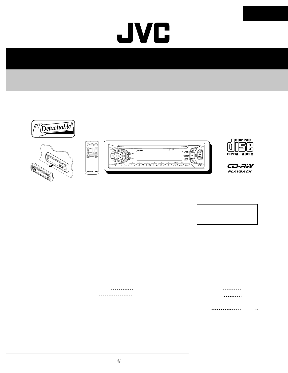
SERVICE MANUAL
CD RECEIVER
KD-S687
KD-S687
Contents
Safety precaution
Preventing static electricity
Disassembly method
Adjustment method
1-2
1-3
1-4
1-11
Area Suffix
UR ------------------- Brazil
Flow of functional
operation unit TOC read
Maintenance of laser pickup
Replacement of laser pickup
Description of major ICs
1-12
1-14
1-14
1-15 26
COPYRIGHT 2002 VICTOR COMPANY OF JAPAN, LTD.
No.49737
Apr. 2002
Page 2
KD-S687
Safety precaution
!
!
Burrs formed during molding may be left over on some parts of the chassis. Therefore,
pay attention to such burrs in the case of preforming repair of this system.
Please use enough caution not to see the beam directly or touch it in case of an
adjustment or operation check.
1-2
Page 3
KD-S687
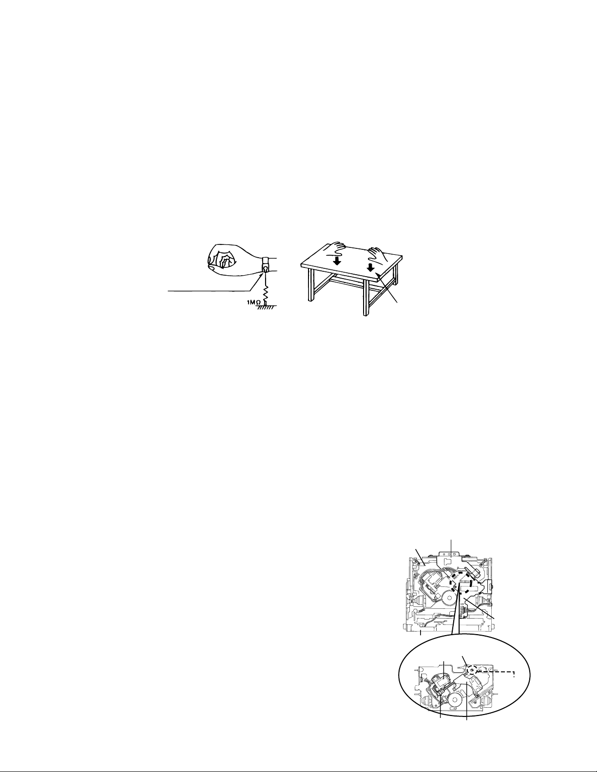
Preventing static electricity
1.Grounding to prevent damage by static electricity
Electrostatic discharge (ESD), which occurs when static electricity stored in the body, fabric, etc. is discharged,
can destroy the laser diode in the traverse unit (optical pickup). Take care to prevent this when performing repairs.
2.About the earth processing for the destruction prevention by static electricity
Static electricity in the work area can destroy the optical pickup (laser diode) in devices such as CD players.
Be careful to use proper grounding in the area where repairs are being performed.
2-1 Ground the workbench
Ground the workbench by laying conductive material (such as a conductive sheet) or an iron plate over
it before placing the traverse unit (optical pickup) on it.
2-2 Ground yourself
Use an anti-static wrist strap to release any static electricity built up in your body.
(caption)
Anti-static wrist strap
Conductive material
3. Handling the optical pickup
1. In order to maintain quality during transport and before installation, both sides of the laser diode on the
replacement optical pickup are shorted. After replacement, return the shorted parts to their original condition.
(Refer to the text.)
2. Do not use a tester to check the condition of the laser diode in the optical pickup. The tester's internal power
source can easily destroy the laser diode.
(conductive sheet) or iron plate
4.Handling the traverse unit (optical pickup)
1. Do not subject the traverse unit (optical pickup) to strong shocks, as it is a sensitive, complex unit.
2. Cut off the shorted part of the flexible cable using nippers, etc. after replacing the optical pickup. For specific
details, refer to the replacement procedure in the text. Remove the anti-static pin when replacing the traverse
unit. Be careful not to take too long a time when attaching it to the connector.
3. Handle the flexible cable carefully as it may break when subjected to strong force.
4. It is not possible to adjust the semi-fixed resistor that adjusts the laser power. Do not turn it
CD mechanism ass’y
Damper bracket
Attention when traverse unit is decomposed
*Please refer to "Disassembly method" in the text for pick-up and how to
detach the substrate.
1.Solder is put up before the card wire is removed from connector on
the CD substrate as shown in Figure.
(When the wire is removed without putting up solder, the CD pick-up
assembly might destroy.)
2.Please remove solder after connecting the card wire with
when you install picking up in the substrate.
Front bracket
Feed motor ass’y
FD screw
CD mechanism
control board
Soldering
FD gear
Pickup unit
1-3
Page 4
KD-S687
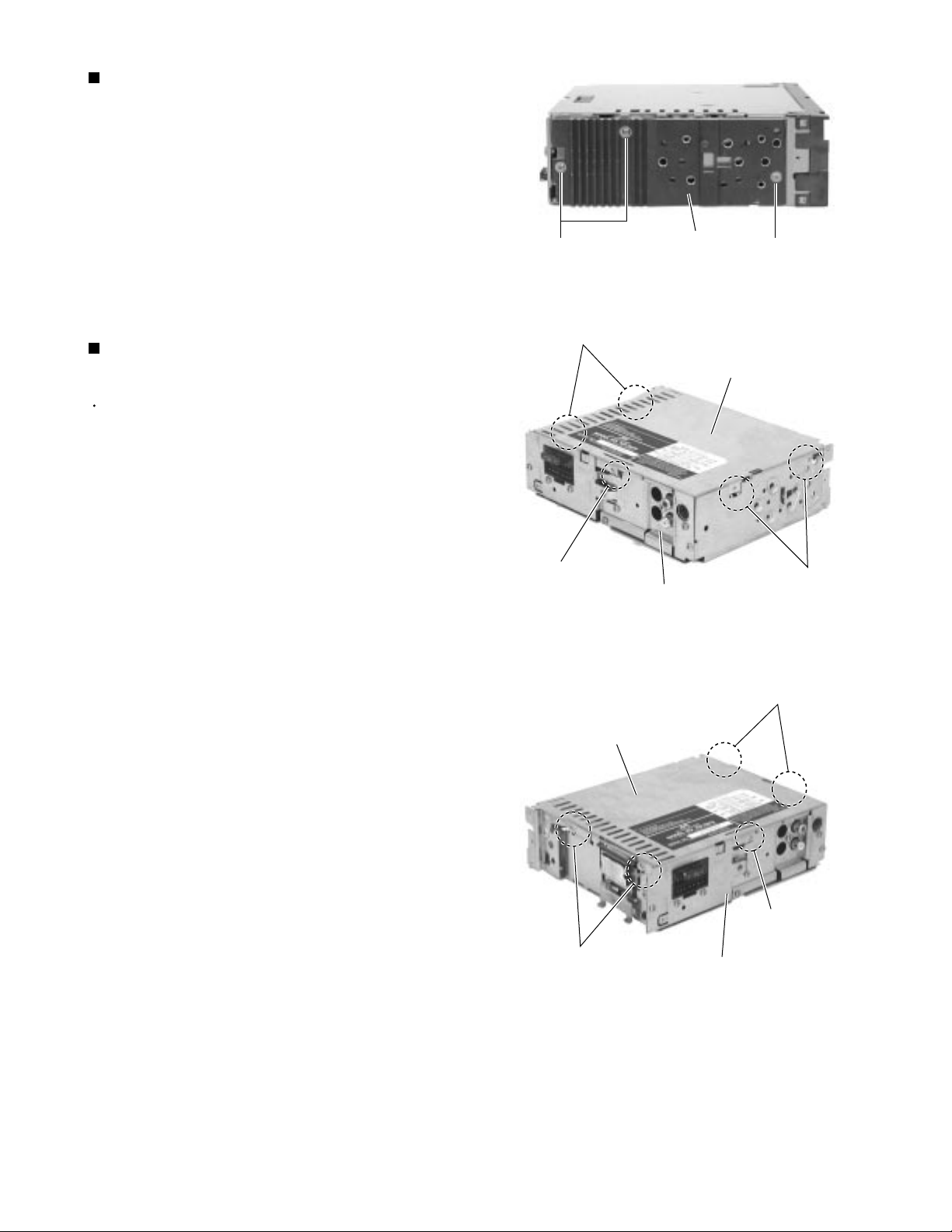
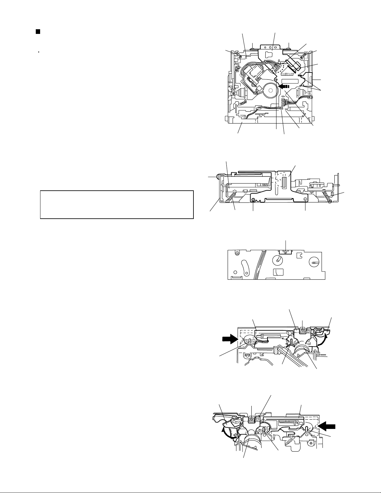
Disassembly method
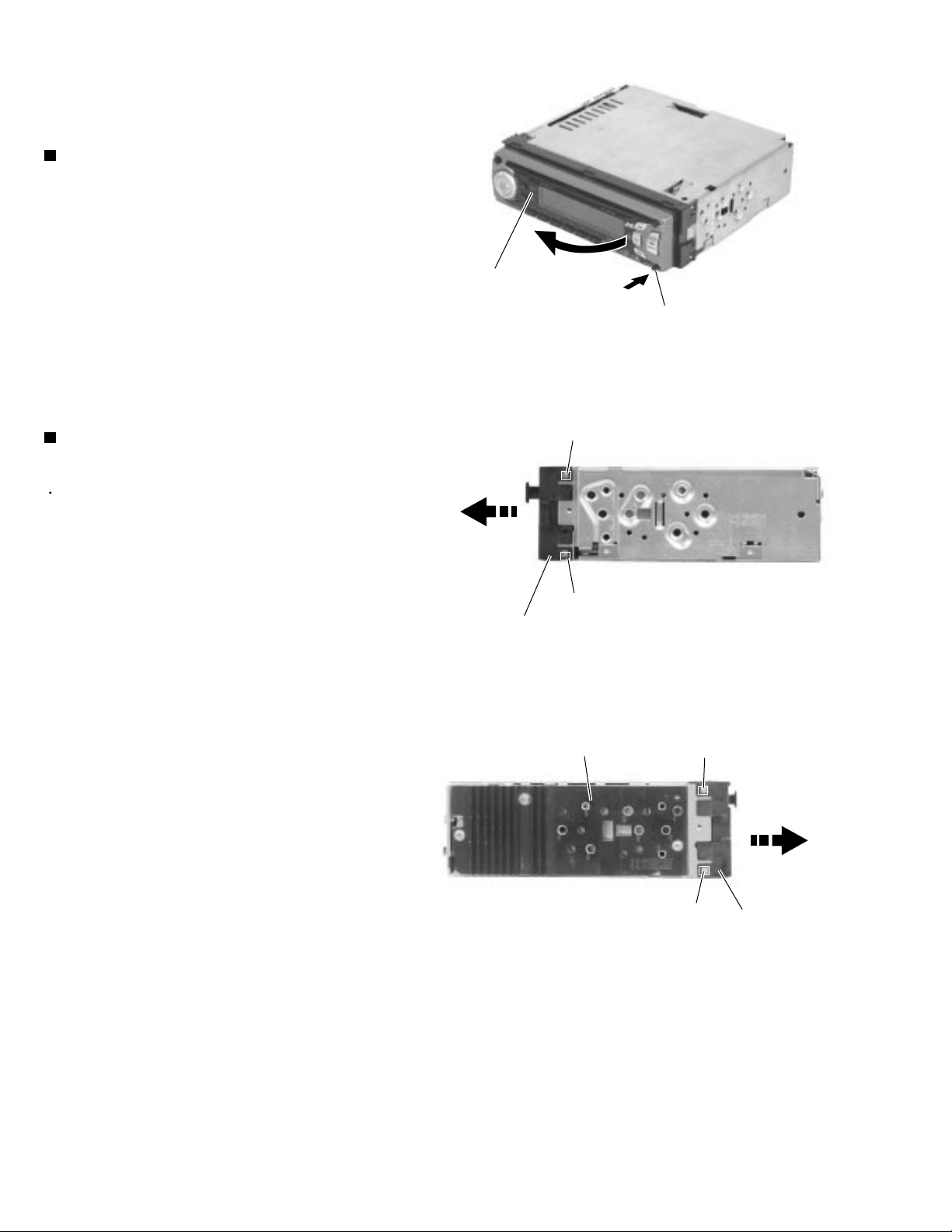
<Main body>
Removing the front panel assembly
(See Fig.1)
1.
Press the eject button in the lower right part of the
front panel. Remove the front panel assembly from
the body.
Front panel assembly
Eject button
Fig.1
Removing the front chassis assembly
(See Fig.2 and 3)
Prior to performing the following procedure, remove
the front panel assembly.
1.
Release the four joint tabs a on both sides of the
front chassis assembly and remove the front chassis
assembly toward the front.
Tab a
Tab a
Front chassis assembly
Heat sink
Fig.2
Tab a
1-4
Fig.3
Tab a
Front chassis
assembly
Page 5
Removing the heat sink (See Fig.4)
1.
Remove the three screws A on the left side of the
body.
KD-S687
Removing the bottom cover
(See Fig.5 and 6)
Prior to performing the following procedure, remove
the front panel assembly, the front chassis assembly
and the heat sink.
1.
Turn over the body and unjoint the five joints b with
the bottom cover and the body using a screwdriver.
A
Joints b
Joint b
Heat sink
Fig.4
Rear panel
Fig.5
A
Bottom cover
Joints b
Bottom cover
Joints b
Joints b
Joint b
Rear panel
Fig.6
1-5
Page 6
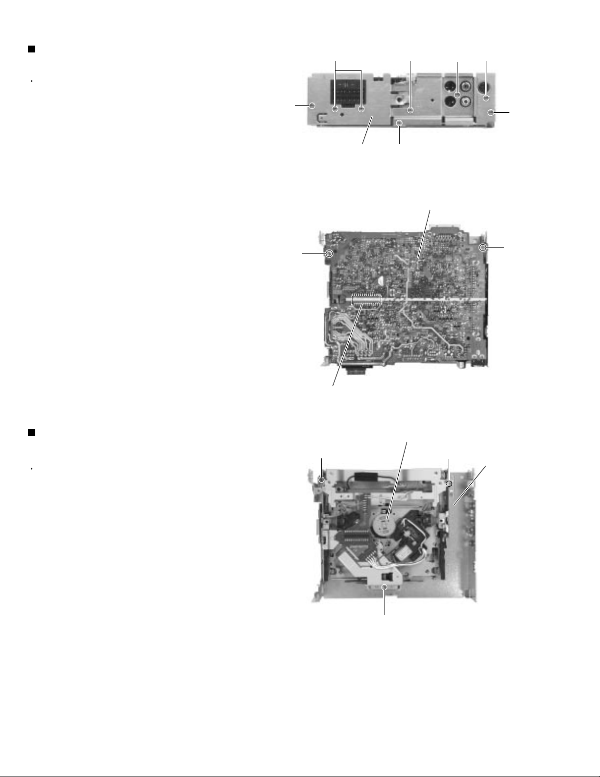
KD-S687
Removing the main board
(See Fig.7 and 8)
Prior to performing the following procedure, remove
the front panel assembly, the front chassis assembly,
the heat sink and the bottom cover.
1.
Remove the screw B, the four screws C and the
three screws D attaching the rear bracket on the
back of the body. Remove the rear panel.
2.
Remove the two screws E attaching the main board
on the bottom of the body. Disconnect connector
CN501 on the main board in the direction of the
arrow.
D
E
Rear panel
CC
D
Fig.7
Main board
B
C
D
E
Removing the CD mechanism section
(See Fig.9)
Prior to performing the following procedure, remove
the front panel assembly, the front chassis assembly,
the heat sink, the bottom cover and the main board.
1.
Remove the three screws F attaching the cassette
mechanism section on the back of the top chassis.
CN501
F
Fig.8
CD mechanism section
F
Fig.9
F
Top chassis
1-6
Page 7
KD-S687
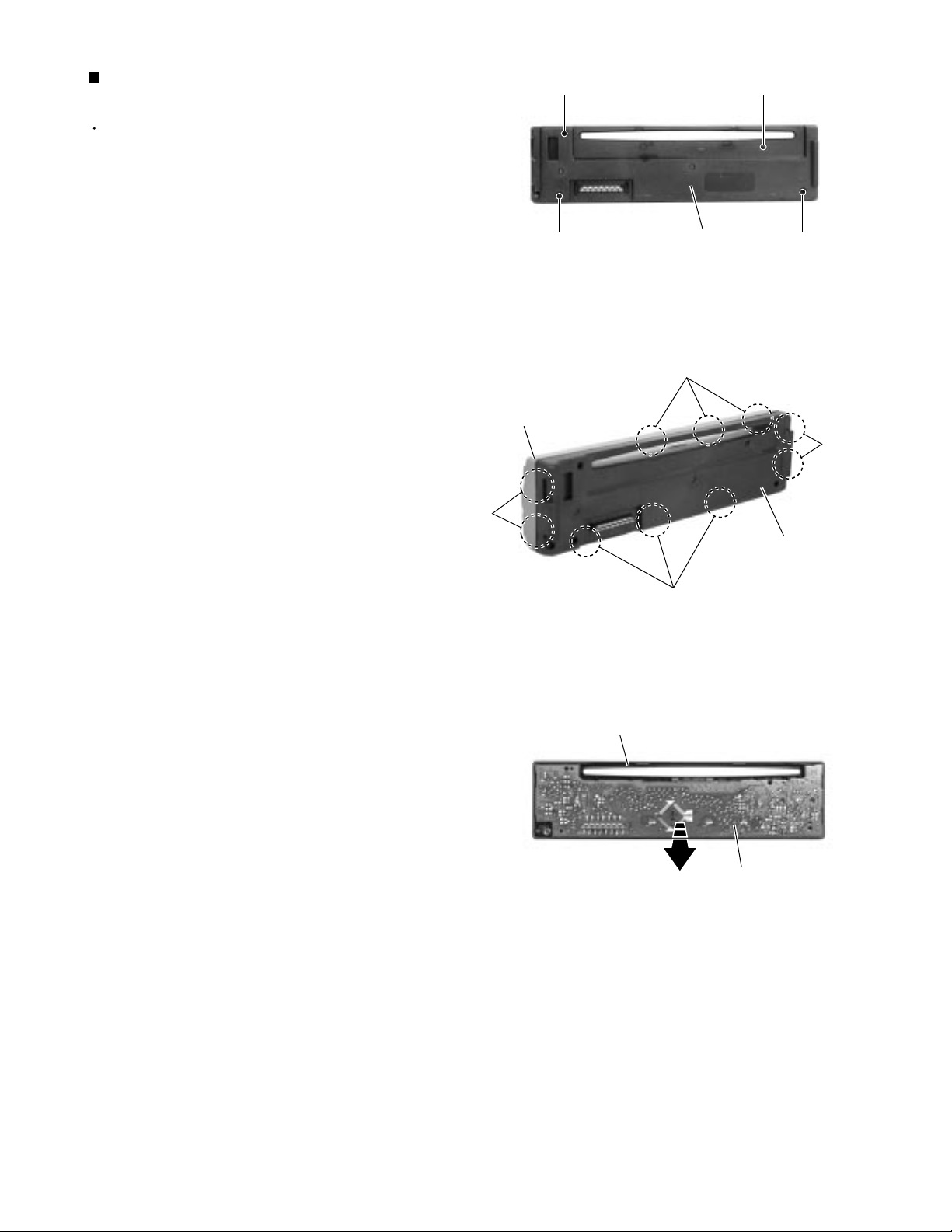
Removing the control switch board
(See Fig.10 to 12)
Prior to performing the following procedure, remove
the front panel assembly.
1.
Remove the four screws G attaching the rear cover
on the back of the front panel assembly.
2.
Unjoint the ten joints c with the front panel and the
rear cover.
3.
Remove the control switch board on the back of the
front panel.
Joints c
Front panel
G
G
Rear cover
Fig.10
Joints c
G
G
Joints c
Front panel
Rear cover
Joints c
Fig.11
Control switch board
Fig.12
1-7
Page 8
KD-S687
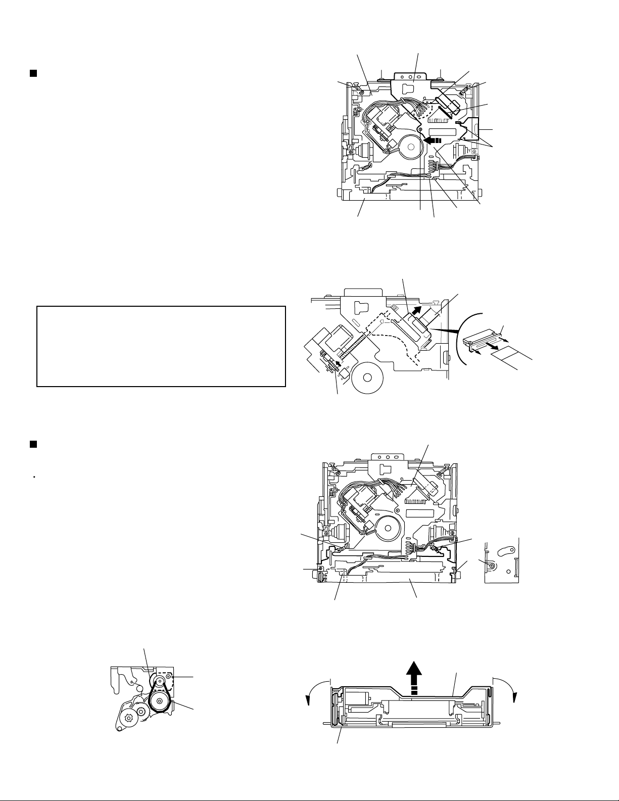
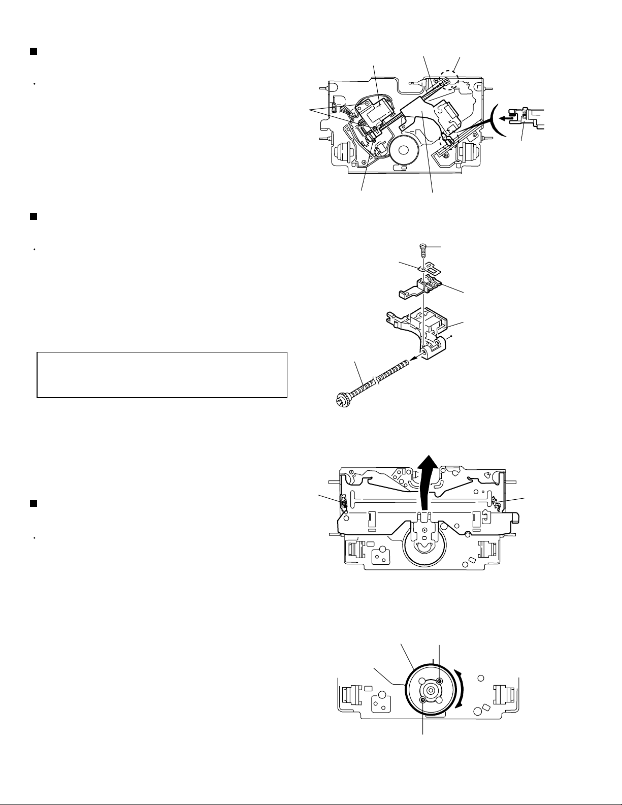
<CD mechanism section>
Removing the CD mechanism control
board (See Fig.1 and 2)
1.
Unsolder the part a and b on the CD mechanism
control board.
2.
Remove the stator fixing the CD mechanism control
board and the damper bracket (To remove the stator
smoothly, pick up the center part).
3.
Remove the screw A attaching the CD mechanism
control board.
4.
Remove the CD mechanism control board in the
direction of the arrow while releasing it from the two
damper bracket slots d and the front bracket slot e.
5.
Disconnect the flexible wire from connector on the
pickup unit.
ATTENTION:
Turn the FD gear in the direction of the
arrow to move the entire pickup unit to
the appropriate position where the
flexible wire of the CD mechanism unit
can be disconnected easily.
(Refer to Fig.2)
CD mechanism assembly
D
h
Front bracket
Pickup unit
Damper bracket
D
A
Fig.1
e
b
Flexible wire
a
h
c
D
d
CD mechanism
control board
Shift the lock
Removing the loading motor
(See Fig.3 to 5)
Prior to performing the following procedure, remove
the CD mechanism control board.
1.
Remove the two springs f attaching the CD
mechanism assembly and the front bracket.
2.
Remove the two screws B and the front bracket
while pulling the flame outward.
3.
Remove the belt and the screw C from the loading
motor.
Loading motor
C
FD gear
f
B
Loading motor
Pull outward
Fig.2
CD mechanism control board
f
B
Front bracket
Fig.3
Front bracket
Pull outward
1-8
Fig.5
Belt
Flame
Fig.4
Page 9
KD-S687
Removing the CD mechanism assembly
(See Fig.1, 6 to 9)
Prior to performing the following procedure, remove
the CD mechanism control board and the front
bracket (loading motor).
1.
Remove the three screws D and the damper
bracket.
2.
Raise the both sides fix arms and move the fix plates
in the direction of the arrow to place the four shafts g
as shown in Fig.8 and 9.
3.
Remove the CD mechanism assembly and the two
springs h attaching the flame.
4.
Remove the two screws E and both sides rear
damper brackets from the dampers. Detach the CD
mechanism assembly from the left side to the right
side.
ATTENTION:
The CD mechanism assembly can be
removed if only the rear damper
bracket on the left side is removed.
CD mechanism
h
Front bracket
CD mechanism
D
Flame
assembly
D
assembly
h
D
Damper bracket
D
A
Fig.5
e
b
Damper bracket
D
Fig.6
a
h
c
D
d
CD mechanism
control board
h
Fix plate (L)
g
Fix arm (R)
D
Fig.7
Rear damper bracket
g
Fig.8
Rear damper bracket
E
Fix plate(R)
E
Fix arm (L)
Damper
Damper
g
g
Fig.9
1-9
Page 10
KD-S687
Removing the feed motor assembly
(See Fig.10)
Prior to performing the following procedure, remove
the CD mechanism control board, the front bracket
(loading motor) and the CD mechanism assembly.
1.
Remove the two screws F and the feed motor
assembly.
Removing the pickup unit
(See Fig.10 and 11)
Prior to performing the following procedure, remove
the CD mechanism control board, the front bracket
(loading motor), the CD mechanism assembly and
the feed motor assembly.
1.
Detach the FD gear part of the pickup unit upward.
Then remove the pickup unit while pulling out the
part i of the FD screw.
Feed motor assembly
F
FD gear
Nut push spring plate
FD screw
Pickup unit
Fig.10
Part i
Part j
Pickup unit
G
Pickup mount nut
Pickup unit
ATTENTION:
2.
Remove the screw G attaching the nut push spring
plate and the pickup mount nut from the pickup unit.
Pull out the FD screw.
When reattaching the pickup unit,
reattach the part j of the pickup unit,
then the part i of the FD screw.
Removing the spindle motor
(See Fig.12 and 13)
Prior to performing the following procedure, remove
the CD mechanism control board, the front bracket
(loading motor), the CD mechanism assembly and
the feed motor assembly.
1.
Turn up the CD mechanism assembly and remove
the two springs k on both sides of the clamper arms.
Open the clamper arm upward.
2.
Turn the turn table, and remove the two screws H
and the spindle motor.
k
FD screw
Spindle motor
Fig.11
k
Fig.12
H
1-10
H
Fig.13
Page 11
Adjustment method
KD-S687
Test instruments required for adjustment
1. Digital oscilloscope (100MHz)
2. AM Standard signal generator
3. FM Standard signal generator
4. Stereo modulator
5. Electric voltmeter
6. Digital tester
7. Tracking offset meter
8. Test Disc JVC :CTS-1000
9. Extension cable for check
EXTGS004-26P 1
Standard measuring conditions
Power supply voltage DC14.4V(10.5~16V)
Load impedance 4 (2 Speakers connection)
Line oout impeadance 20k
Output Level Line out 2.0V (Vol. MAX)
How to connect the extension cable for adjusting
Standard volume position
Balance and Bass &Treble volume : lndication"0"
Loudness : OFF
BBE : OFF
Frequency Band
FM 87.5MHz ~ 107.9MHz
MW 530kHz ~ 1710 kHz
Dummy load
Exclusive dummy load should be used for AM,and FM. For
FM dummy load,there is a loss of 6dB between SSG output
and antenna input.The loss of 6dB need not be considered
since direct reading of figures are applied in this working
standard.
EXTGS004-26P
1-11
Page 12
KD-S687
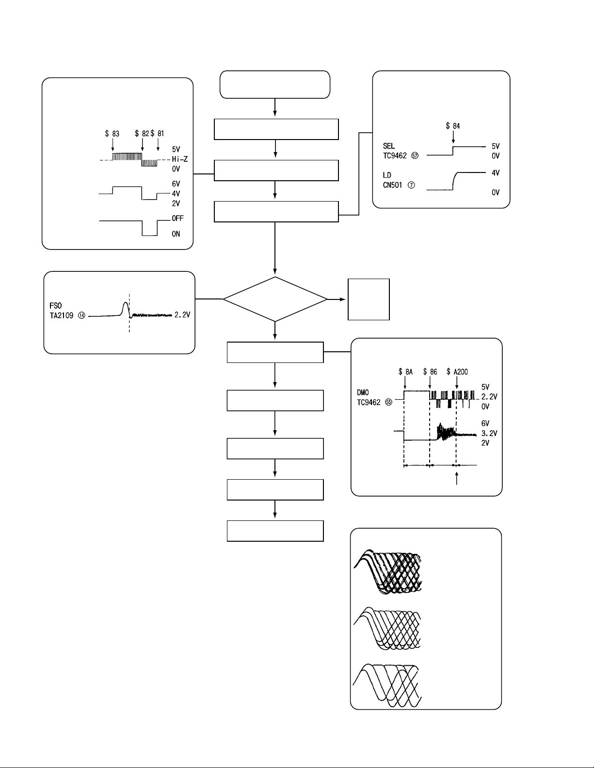
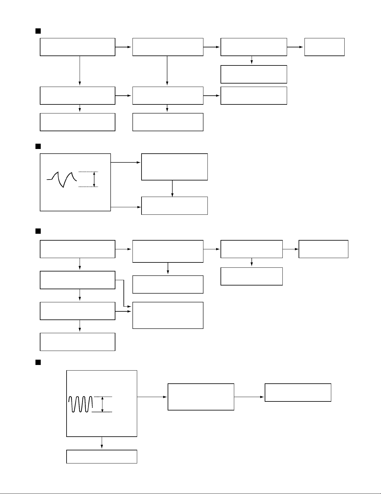
Flow of functional operation until TOC read
Power ON
• When the pickup correctly moves
to the inner area of the disc
Set Function to CD
• When the laser diode correctly
emits
Microprocessor
commands
FMO
TC9462 "53"
FEED MOTOR
+TERMINAL
TERMINAL
IC581 "5"
REST SW
• When correctly focused
Focus Servo Loop ON
Disc inserted
Pickup feed to the inner area
Laser emitted
Focus search
Disc rotates
RF signal eye-pattern
remains closed
Tracking loop closed
RF signal eye-pattern
opens
TOC readout
YES
YES
Microprocessor
commands
"No disc"
display
• When the disc correctly rotates
Microprocessor
commands
Spindle
motor (-)
IC581 "7"
AccelerationAcceleration
0.5 Sec
Rough
Servo
0.5 Sec
Servo CLV
1-12
Jump to the first track
Play
Tracking Servo Loop ON
• RF signal
Rough Servo Mode
CLV Servo Mode
(ProgramArea)
CLV Servo Mode
(Lead-In Area;
Digital: 0)
Page 13
Feed Section
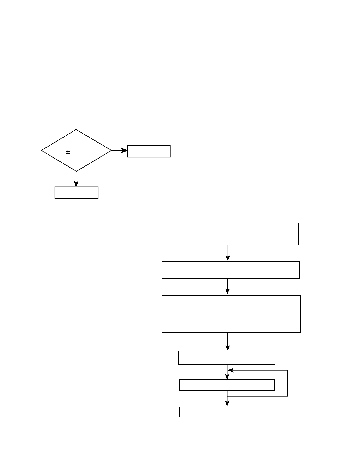
Is the voltage output at
IC521 pin "53" 5V or 0V?
YES
Is 4V present at both
sides of the feed motor?
YES
NO
Is the wiring for IC521
(90) ~ (100) correct?
NO
Is 6V or 2V present at
IC581 "5" and "6"?
NO
YES
YES
Is 5V present at IC581
pin "11"?
YES
Check the vicinity of
IC521.
Check the feed motor
connection wiring.
NONO
KD-S687
Check CD 9V
and 5V.
Check the feed motor.
Focus Section
When the lens is
moving:
4V
Does the S-search
waveform appear at
IC581 pins "17" and "18"?
Spindle Section
Is the disk rotated?
YES
Does the RF signal
appear at TP1?
YES
Check IC581.
NO
YES
NO
NO
Check the circuits in
the vicinity of IC581
pins "15" ~ "18".
Check the pickup and
its connections.
Is 4V present at IC581
pins "7" and "8" ?
Check the spindle motor
and its wiring.
YES
YES
NO NO
Is 4V present at IC521
pin "55" ?
YES
Check the vicinity of
IC581.
Check IC501 and
IC521.
Is the RF waveform at TP1
distorted?
YES
Proceed to the Tracking
section
Tracking Section
When the disc is rotated
at first:
Is the tracking error signal
output at IC501 "12"?
Check IC521.
NO
Approx. 1.2 V
YES
Check the circuits in the
vicinity of IC501 "19" ~
"24" or the pickup
Check the circuit in the
vicinity of IC501 pins
"2" ~ "12".
YESYES
Check the pickup and
its connections.
1-13
Page 14
KD-S687
Maintenance of laser pickup
(1) Cleaning the pick up lens
Before you replace the pick up, please try to
clean the lens with a alcohol soaked cotton
swab.
(2) Life of the laser diode
When the life of the laser diode has expired,
the following symptoms will appear.
(1) The level of RF output (EFM output:ampli
tude of eye pattern) will be low.
Is RF output
1.0 0.35Vp-p?
YES
O.K
(3) Semi-fixed resistor on the APC PC board
The semi-fixed resistor on the APC printed
circuit board which is attached to the pickup
is used to adjust the laser power.Since this
adjustment should be performed to match the
characteristics of the whole optical block,
do not touch the semi-fixed resistor.
If the laser power is lower than the specified
value,the laser diode is almost worn out, and
the laser pickup should be replaced.
If the semi-fixed resistor is adjusted while
the pickup is functioning normally,the laser
pickup may be damaged due to excessive current.
NO
Replace it.
Replacement of laser pickup
Turn off the power switch and,disconnect the
power cord from the ac outlet.
Replace the pickup with a normal one.(Refer
to "Pickup Removal" on the previous page)
Plug the power cord in,and turn the power on.
At this time,check that the laser emits for
about 3seconds and the objective lens moves
up and down.
Note: Do not observe the laser beam directly.
1-14
Play a disc.
Check the eye-pattern at TP1.
Finish.
Page 15
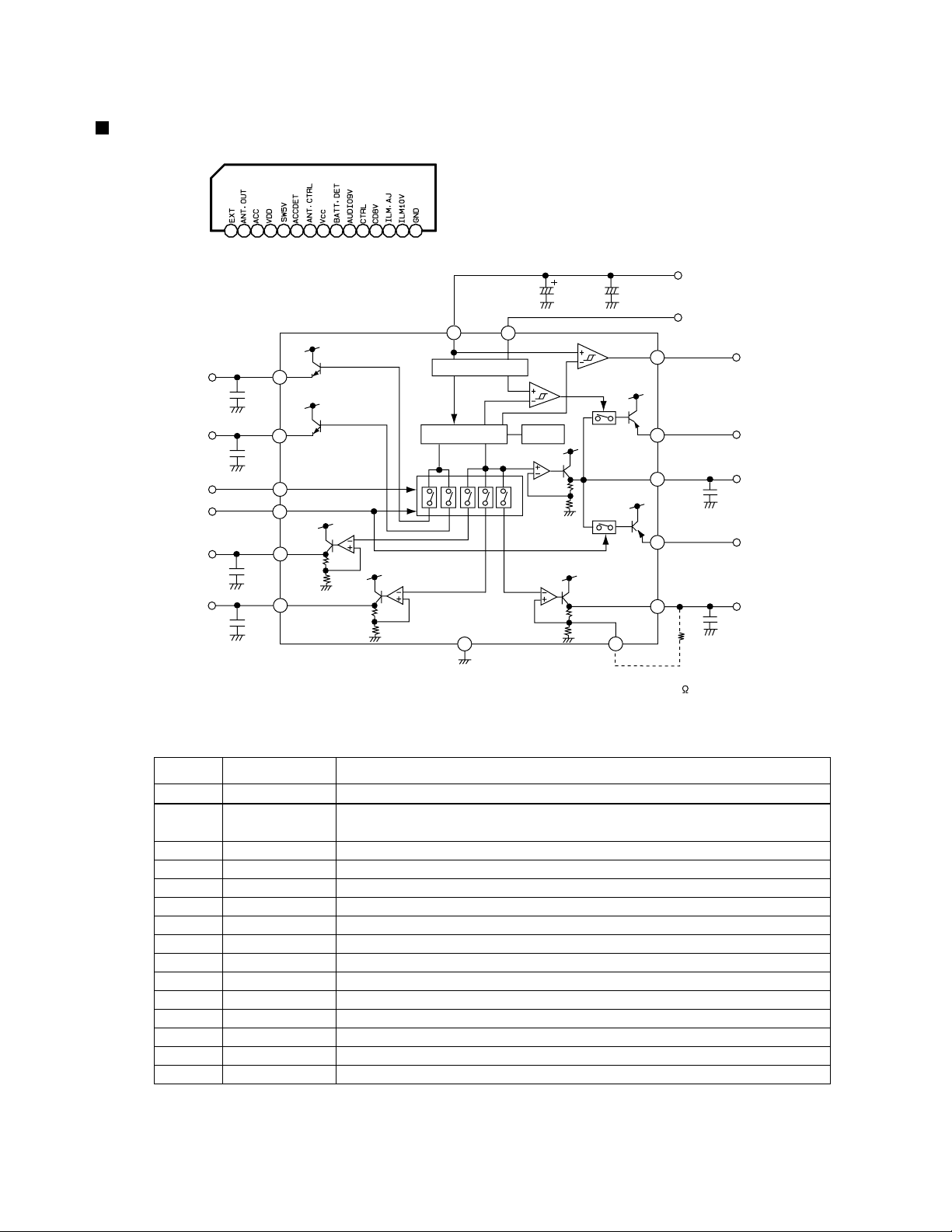
Description of major ICs
HA13164 (IC901) : Regulator
1.Terminal layout
123456789101112131415
KD-S687
2.Block diagram
3.Pin function
ANT OUT
C3
0.1u
EXT OUT
C4
0.1u
ANT CTRL
CTRL
CD OUT
C5
0.1u
AUDIO OUT
C6
10u
11
12
10
BATT.DET OUT
9
COMPOUT
6
VDD OUT
4
SW5VOUT
5
14
UNIT R:
+B
ACC
ILMOUT
R1
C7
0.1u
C8
0.1u
C1
100u
VCC ACC
8
2
1
7
Surge Protector
BIAS TSD
15
3
note1) TAB (header of IC)
connected to GND
ILM AJGND
13
C2
0.1u
C:F
Pin No. Symbol Function
1
2
EXTOUT
ANTOUT
Output voltage is VCC-1 V when M or H level applied to CTRL pin.
Output voltage is VCC-1 V when M or H level to CTRL pin and H level
to ANT-CTRL.
3
4
5
6
7
8
9
10
11
12
13
14
15
ACCIN
VDDOUT
SW5VOUT
COMPOUT
ANT CTRL
VCC
BATT DET
AUDIO OUT
CTRL
CD OUT
ILM AJ
ILM OUT
GND
Connected to ACC.
Regular 5.7V.
Output voltage is 5V when M or H level applies to CTRL pin.
Output for ACC detector.
L:ANT output OFF , H:ANT output ON
Connected to VCC.
Low battery detect.
Output voltage is 9V when M or H level applied to CTRL pin.
L:BIAS OFF, M:BIAS ON, H:CD ON
Output voltage is 8V when H level applied to CTRL pin.
Adjustment pin for ILM output voltage.
Output voltage is 10V when M or H level applies to CTRL pin.
Connected to GND.
1-15
Page 16

KD-S687
BD3860K (IC161):E.Volume
1.Terminal layout
33 23
2.Blockdiagram
GND FIL VCC SEL1
6 5 9 40 36 35 343328323130 2919 15 14
POWER
SUPPLY
A1
41
B1
42
C1
43
D1
44
INPUT
1
2
3
4
SELECTOR
A2
B2
C2
D2
34
44
1 11
INPUT
GAIN
0 18 dB
INPUT
GAIN
0 18 dB
22
12
VIN1 LOUD1 HF1 LF1 DET1 TIN1 TNF1 BNF1
MAIN
VOLUME
0 -40 dB
LOUDNESS
MAIN
VOLUME
0 -40 dB
LOUDNESS
LOW(f=50Hz) 6dB
PROCESS CONTROL +3 to 12dB
(f=10kHz)
LOGIC
LOW(f=50Hz) 6dB
PROCESS CONTROL +3 to 12dB
(f=10kHz)
TREBLE
-14 +14dB
TREBLE
-14 +14dB
-14 +14dB
-14 +14dB
BASS
BASS
BOUT1VCA1 MIX1 BBOUT1
FADER
CH1 FRONT
0 -5 dB
FADER
CH1 REAR
0 -5 dB
FADER
CH2 REAR
0 -5 dB
FADER
CH2 FRONT
0 -5 dB
13
12
10
11
7
8
OUTF1
OUTR1
SI
SC
OUTR2
OUTF2
3.Pin function
Pin
Symbol Function
No.
1
2
3
4
5
6
7
8
9
10
11
12
13
14
15
16
17
18
19
20
21
22
A2
B2
C2
D2
FIL
GND
SI
SC
VCC
OUTR2
OUTF2
OUTR1
OUTF1
BOUT1
BNF1
BOUT2
BNF2
TNF2
TNF1
TIN2
BBOUT2
MIX2
CH2 Input Pin A
CH2 Input Pin B
CH2 Input Pin C
CH2 Input Pin D
1/2 VCC Pin
Ground Pin
Serial Data Receiving Pin
Serial Clock Receiving Pin
Power Supply Pin
CH2 Rear Output Pin
CH2 Front Output Pin
CH1 Rear Output Pin
CH1 Front Output Pin
CH1 Bass Filter Setting Pin
CH1 Bass Filter Setting Pin
CH2 Bass Filter Setting Pin
CH2 Bass Filter Setting Pin
CH2 treble Filter Setting Pin
CH1 treble Filter Setting Pin
CH2 treble Input Pin
CH2 BBE II Signal Output Pin
CH2 Output MIX Amplifier
Inverse Input Pin
39 38 37 25 24 26 23 22 21 20 18 17 16
Pin
Symbol Function
No.
23
24
25
26
27
28
29
30
BBOUT1
31
32
33
34
35
LOUD1
36
37
LOUD2
38
39
40
41
42
43
44
VCA2
LF2
HF2
DET2
NC
DET1
TIN1
MIX1
VCA1
LF1
HF1
VIN1
VIN2
SEL2
SEL1
A1
B1
C1
D1
CH2 High Pass VCA Output Pin
CH2 Low Pass Filter Setting Pin
CH2 High Pass Filter Setting Pin
CH2 High Pass Attack/Release Time Setting Pin
Non connect
CH1 High Pass Attack/Release Time Setting Pin
CH1 treble Input Pin
CH1 BBE II Signal Output Pin
CH1 Output MIX Amplifier Inverse Input Pin
CH1 High Pass VCA Output Pin
CH1 Low Pass Filter Setting Pin
CH1 High Pass Filter Setting Pin
CH1 Loudness Filter Setting Pin
CH1 Main Volume Input Pin
VCH2 Loudness Filter setting Pin
CH2 Main Volume Input Pin
CH2 Input Gain Output Pin
CH1 Input Gain output Pin
CH1 Input Pin A
CH1 Input Pin B
CH1 Input Pin C
CH1 Input Pin D
BOUT2BNF2TNF2TIN2BBOUT2MIX2VCA2DET2LF2HF2LOUD2VIN2SEL2
1-16
Page 17

LA6574H-X (IC561) : Power AMP
1.Pin layout / Block diagram
KD-S687
VCC2 1
V05- 2
V05+ 3
V04+ 4
V04- 5
V03+ 6
V03- 7
FR FR
V02+ 8
V02- 9
CH5
POWER
CH5
CH4
CH3
CH2
Thermal Shuydown
Level Shift Level Shift Level Shift Level ShiftOutput Control
Input
22k 11k
Signal System Power
3.3VREG (External
PNP Tr)
28 REV
27 FWD
26 S-GND
25 VCONT
24 VIN4
23 VIN4G
22 VCC-S
FR FR
21 VREF-IN
20 REG-OUT
V01+ 10
V01- 11
VCC1 12
VIN1 13
VIN1G 14
CH1
CH1.2.3.4
POWER
11k
22k
11k
22k
22k
11k
19 REG-IN
18 VIN3G
17 VIN3
16 VIN2G
15 VIN2
2.Pin function
PinNo. Symbol Function PinNo. Symbol Function
1
2
3
4
5
6
7
8
9
10
11
12
13
14
VCC2
VO5VO5+
VO4+
VO4VO3+
VO3VO2+
VO2VO1+
VO1VCC1
VIN1
VIN1G
CH3,4,5 power supply
Loading output (
Loading output (
CH4 output terminal (
CH4 output terminal (
CH3 output terminal (
CH3 output terminal (
CH2 output terminal (
)
)
)
)
)
)
)
CH2 output terminal ( )
CH1 output terminal (
)
CH1 output terminal ( )
CH1,2 power supply
CH1 input terminal
CH1 input terminal (For gain ADJ)
15
16
17
18
19
20
21
22
23
24
25
26
27
28
VIN2
VIN2G
VIN3
VIN3G
REG-IN
REG-OUT
VREF-IN
VCC-S
VIN4G
VIN4
VCONT
S-GND
FWD
REV
CH2 input terminal
CH2 input terminal (For gain ADJ)
CH3 input termianl
CH3 input terminal (For gain ADJ)
Regulator terminal
Regulator terminal
Reference voltage input terminal
Signal system power supply
CH4 input terminal (For gain ADJ)
CH4 input terminal
5CH output voltage setting terminal
GND for signal line
5CH output select terminal
5CH output select terminal
1-17
Page 18

KD-S687
UPD178078GF-559 (IC701) : System CPU
81
~
BUSINT
BUSSI
BUSSO
JBUS-SCK
VOL-DA
VOL-CLK
LCDDA
LCDCLK
BUSI/O
LCDCE
SW2
SW3
SW4
RSTSW
ENC1
ENC2
KEY0
KEY1
KEY2
LEVEL
AVDD
SM
AVSS
REGCPU
VDD
REGOSC
X2
X1
GND0
SD/ST
GND2
IFC
VDDPLL
OSC
80 ~ 51
50
~
31
1 ~ 30
1.Pin layout
100
2.Pin function (1/2)
Pin
NO.
1
2
3
4
5
6,7,8
9
10
11
12
13
14
15
16
17
18
19
20
21
22
23
24
25
26
27
28
29
30,31
32
33
34
35
36
37
38
39
40
41
42
43
44
45
I/OSymbol FUNCTION
-
No use
I
JVC bus communication line
I
JVC bus communication line
O
JVC bus communication line
O
JVC bus communication line
-
No use
O
Serial data for volume
O
Serial clock for volume
-
No use
O
LCD driver serial data output
O
Serial data for LCD
O
JVC bus output select
-
No use
O
LCD driver communication line
I
CD mech switch
I
CD mech switch
I
CD mech switch
I
Traverse mech rest switch
I
Encoder input
I
Encoder input
I
Key input
I
Key input
I
Key input
I
Audio level input
-
Power supply
I
Signal level meter input
-
No use
-
No use
-
Connect to GND
-
Connect to GND with capacitor
-
Power supply
-
Connect to GND with capacitor
-
System clock
I
System clock
-
Connect to GND
I
Station detector & Stereo indicator
-
Connect to GND
-
No use
I
IF count input
-
---
I
FM,AM osc input
-
No use
1-18
Page 19

KD-S687
2.Pin function (2/2)
Pin
NO.
46
GNDPLL
47
AMEO
48
FMEO
49
IC(VPP)
50
RESET
51
SW1
52
REMOCON
53
VTR-LOGIC
54
VR-CONT
55
POWER
56
CDON
57
MUTE
58
STAGE
59
BUZZER
60
JAPAN
61~67
68
CDRW
69
LM0
70
LM1
71
BUCK
72
CCE
73
BUS0
74
BUS1
75
BUS2
76
BUS3
77
RST
78
PS1
79
PS2
80
DETACH
81
82
GND1
83
MONO
84
SEEK/STOP
85
FM/AM
86
87
ANT
88
TEL MUTE
89~98
100
99
NC
VDDPORT
GNDPORT
I/OSymbol FUNCTION
-
---
O
PLL error output for AM
O
PLL error output for FM
-
Setting to write for flash
I
System reset
I
CD mech switch
I
Remocon input
-
No use
-
No use
O
Power control
O
CD power control
O
Mute control
-
No use
-
No use
-
No use
-
No use
O
CD-RW detect signal output
O
CD mech driver control
O
CD mech driver control
O
CD LSI communication line
O
CD LSI communication line
I/O
I/O
I/O
I/O
CD LSI communication line
CD LSI communication line
CD LSI communication line
CD LSI communication line
O
CD LSI communication line
I
ACC detection input
I
Memory detection
I
Detach detection
-
No use
-
Connect to GND
O
Mono by force
O
Switching SEEK & STOP
O
Band switch
-
No use
O
Antena regulator control signal
-
No use
-
Non connection
-
Vdd
-
Connect to GND
UPD178078GF-559
1-19
Page 20

KD-S687
LA4743K(IC302):Power AMP
1.Block diagram
IN 1
TA B
IN 2
+
0.22 F
+
0.22 F
11
1
12
Vcc 1/2 Vcc 3/4
6 20
-
+
Protective
circuit
-
+
2200 F 0.022 F
+
9
7
+
OUT 1+
OUT 1-
PWR GND1
8
+
OUT 2+
5
-
OUT 2-
3
PWR GND2
2
ST BY
R.F
47 F
IN 3
PRE GND
IN 4
+5V
ST ON
+
0.22 F
N.C
+
0.22 F
4
Stand by
Switch
Mute
10
+
Ripple
Filter
Mute
22
circuit
3.3 F
+
15
-
+
-
17
19
10K
+
OUT 3+
OUT 3-
Low Level
Mute ON
25
18
21
23
PWR GND3
OUT 4+
OUT 4-
13
14
Protective
circuit
-
+
+
-
1-20
ON TIME C
22 F
Muting &
16
+
ON Time Control
Circuit
PWR GND4
24
Page 21

2.Terminal layout
KD-S687
3.Pin function
1
2
3
4
5
6
7
8
9
10
11
12
13
14
15
16
17
18
19
20
21
22
23
24
25
SymbolPin No. Function
TA B
GND
OUTRRSTBY
OUTRR+
VCC1/2
OUTRFGND
OUTRF+
RIPPLE
INRF
INRR
SGND
INLR
INLF
ONTIME
OUTLF+
GND
OUTLFVCC3/4
OUTLR+
MUTE
OUTLRGND
NC
Header of IC
Power GND
Outpur(-) for front Rch
Stand by input
Output (+) for front Rch
Power input
Output (-) for rear Rch
Power GND
Output (+) for rear Rch
Ripple filter
Rear Rch input
Front Rch input
Signal GND
Front Lch input
Rear Lch input
Power on time control
Output (+) for rear Lch
Power GND
Output (-) for rear Lch
Power input
Output (+) for front
Muting control input
Output (-) for front
Power GND
Non connection
LA4743K
1-21
Page 22

KD-S687
PT6523LQ(IC601) :
1.Terminal layout
48 ~ 33
49
32
64
2.Block diagram
1 ~ 16
17
COMMON
DRIVER
CLOCK
GENERATOR
ADDRESS
DETECTOR
SEGMENT DRIVER & LATCH
SHIFT REGISTER
3.Piin function
Pin No.
1~ 52
53~55
56
57
58
59
60
61
62
63
64
Pin Name
SG1 ~ SG52
COM1 ~ COM3
VDD
INH
VDD1
VDD2
VSS
OSC
CE
CLK
DI
I/O Description
O
O
-
Segment Output Pins
Common Driver Output Pins
Power Supply
Display OFF Control Input Pin
When this pin is "Low", the Display is forcibly
I
turned OFF. (SG1 to SG52, COM1 to COM3 are
set to "LOW"). (See Note 1)
When this pin is set to "High", the Displa is ON.
I
Used for the 2/3 Bias Voltage when the Bias Voltages
are provied externally. Connect to VDD2 when
1/2 Bias is used.
I
Used for 1/3 Bias Voltage when the Bias Voltages
are provided externally. Connect to VDD1 when
1/2 Bias is used.
-
I/O
I
I
I
Ground Pin.
Oscillation Input /Outout Pin
Chip Enable Pin
Synchronization Clock
Transfer Data Pin
1-22
Note 1. When INH = "LOW" : Serial data trensfers can be performed when the display is forcibly OFF.
Page 23

TA2147F-X (IC501) : RF amp
1. Pin layout & Block diagram
GND
RFN
RFO
AGCIN
RFGC
RFGO
RFRPIN
RFRP
FEN
FEO
KD-S687
VRO
GVSW
cc
24
1
V
3 k
3 k
23
40 pF
20 k
2
FNI
180 k
60 k
80 k
22
180 k
40 pF
60 k
20 k
3
FPI
30 k
80 k
2
21
1
4
TPI
0.5
20 k
240 k
15 pF
2
20
k
0.5
5
TNI
240 k
15 pF
19
1.75 k
6
MDI
40 k
14 k
2 k
18
BOTTOM
PEAK
1 k
7
LDO
20 k
1.3 V
60 A
12 k
17
50 k
8
SEL
12 k
2 k
20 k
50 A
16
40 k
9
TEBC
10 pF
15 k
20 k
20 k
15
10 pF
10
TEN
20 k
40 k
14
20 A
11
TEO
13
20 k 20 k
PEAK
50 k 15 k
12
RFDC
2. Pin function
Pin
Symbol I/O Function
No.
1
2
3
4
5
6
MDI
7
LDO
8
SEL
9
TEBC
10
11
12
13
14
15
16
17
18
19
20
21
22
23
24
TEN
TEO
RFDC
GVSW
VRO
FEO
FEN
RFRP
RFRPIN
RFGO
RFGC
AGCIN
RFO
RFN
GND
Vcc
FNI
FPI
TPI
TNI
-
3.3V power supply pin
I
Main-beam amp input pin
I
Main-beam amp input pin
I
Sub-beam amp input pin
I
Sub-beam amp input pin
I
Monitor photo diode amp input pin
O
Laser diode amp output pin
I
APC circuit ON/OFF control signal, laser diode control signal input
or bottom/peak detection frequency change pin
I
Tracking error balance adjustment signal input pin
I
Tracking error signal generation amp negative-phase input pin
O
Tracking error signal generation amp output pin
O
RF signal peak detection output pin
I
AGC/FE/TE amp gain change pin
O
Reference voltage output pin
O
Focus error signal generation amp output pin
I
Focus error signal generation amp negative-phase input pin
O
Signal amp output pin for track count
I
Signal generation amp input pin for track count
O
RF signal amplitude adjustment amp output pin
I
RF amplitude adjustment control signal input pin
I
RF signal amplitude adjustment amp input pin
O
RF signal generation amp output pin
I
RF signal generation amp input pin
-
GND pin
1-23
Page 24

KD-S687
TC9490FA (IC521) : DSP
1. Pin layout & Block diagram
DD3
XO
XV
48 47 46 45 44 43 42 41 40 39 38 37 36 35 34 33
SS3
XI
XV
TESIN
DD3VSS3
V
DMO
FMO
AV
DD3
SEL
TEBC
RFGC
REF
V
TRO
FOO
2. Pin function (1/2)
No. Symbol
1
2
3
4
5
6
7
8
9
10
11
12
13
14
15
16
17
18
19
20
21
22
23
24
25
BCK
LRCK
AOUT
DOUT
IPF
VDD3
VSS3
SBOK
CLCK
DATA
SFSY
SBSY
/HSO
/UHSO
PVDD3
PDO
TMAX
LPFN
LPFO
PVREF
VCOF
AVSS3
SLCO
RFI
AVSS3
49DV
SS3
RO
50
51
DV
DD3
DVR
DV
DD3
ZDET
V
SS5
BUS0
BUS1
BUS2
BUS3
BUCK
/CCE
/RST
V
DD5
LO
LPF
52
53
54
55
56
57
58
59
60
61
62
63
64
1 2 3 4 5 6 7 8 9 10 11 12 13 14 15 16
BCK
I/O
O
Bit clock output pin.32fs, 48fs, or 64fs selectable by command.
O
L/R channel clock output pin. "L" for L channel and "H" for R channel.
O
Audio data output pin. MSB-first or LSB-first selected by command.
O
Digital data output pin. Outputs up to double-speed playback.
O
Correction flog output pin.
-
Digital 3.3V power supply voltage pin.
-
Digital GND pin.
O
Subcode Q data CRCC result output pin. "H" level when result is OK.
I/O
Sub-code P-W data read clock I/O pin. I/O polarity selectable by command.
O
Sub-code P-W data output pin.
O
Playback frames sync signal output pin.
O
Sub-code block sync output pin.
O
Playback speed mode flag output pin.
O
Playback speed mode flag output pin.
-
PLL-only 3.3V power supply voltage pin.
O
EFM and PLCK phase difference signal output pin.
O
TMAX detection result output pin.
I
Inverted input pin for PLL RF amp.
O
Output pin for PLL LPF amp.
-
PLL-only VREF pin.
O
VCO filter pin.
-
Analog GND pin.
O
DAC output pin for data slice level generation.
I
RF signal input pin.
-
Analog 3.3V power supply voltage pin.
generator
Microcontroller
interface
LRCK
Clock
AOUT
1-bit
DAC
circuit
Correction
Audio output
circuit
IPF
DOUT
Address
circuit
16 k
RAM
Digital output
SS3
DD3
V
V
PWM
SBOK
Servo control
ROM
RAM
CLV servo
Sync signal
protection
EFM
Sub code
decoder
DATA
CLCK
Function
Digital equalizer
automatic
adjustment circuit
SFSY
SBSY
/HSO
A/D
VCO
PLL
TMAX
D/A
Data
slicer
/UHSO
PV
DD3
PDO
32
TEZI
31
TEI
30
SBAD
29
FEI
28
RFRP
27
RFZI
26
RFCT
AV
25
DD3
24
RFI
23
SLCO
AV
22
SS3
21
VCOF
PV
20
REF
19
LPFO
18
LPFN
TMAX
17
1-24
Page 25

KD-S687
2. Pin function (2/2)
No. Symbol
26
27
28
29
30
31
32
33
34
35
36
37
38
39
40
41
42
43
44
45
46
47
48
49
50
51
52
53
54
55
56
57
58
59
60
61
62
63
64
RFCT
RFZI
RFRP
FEI
SBADTEI
TEI
TEZI
FOO
TRO
VREF
RFGC
TEBC
SEL
AVDD3
FMO
DMO
VSS3
VDD3
TESIN
XVSS3
XI
XO
XVDD3
DVSS3
RO
DVDD3
DVR
LO
DVSS3
ZDET
VSS5
BUS0
BUS1
BUS2
BUS3
BUCK
/CCE
/RST
VDD5
I/O
I
RFRP signal center level input pin.
I
RFRP signal zero-cross input pin.
I
RF ripple signal input pin.
I
Focus error signal input pin.
I
Sub-beam adder signal input pin.
I
Tracking error input pin. Inputs when tracking servo is on.
I
Tracking error signal zero-cross input pin.
O
Focus equalizer output pin.
O
Tracking equalizer output pin.
-
Analog reference power supply voltage pin.
O
RF amplitude adjustment control signal output pin.
O
Tracking barance control signal output pin.
O
APC circuit ON/OFF signal output pin.
-
Analog 3.3V power supply voltage pin.
O
Feed equalizer output pin.
O
Disc equalizer output pin.
-
Digital GND pin.
-
Digital 3.3V power supply voltage pin.
I
Test input pin.
-
System clock oscillator GND pin.
I
System clock oscillator input pin.
O
System clock oscillator output pin.
-
System clock oscillator 3.3V power supply voltage pin.
-
DA converter GND pin.
O
R-channel data foward output pin.
-
DA converter 3.3V power supply pin.
-
Reference voltage pin.
O
L-channel data forward output pin.
-
DC converter GND pin.
O
1 bit DA converter zero data detection flag output pin.
-
Microcontroller interface GND pin.
I/O
Microcontroller interface data I/O pins.
I/O
Microcontroller interface data I/O pins.
I/O
Microcontroller interface data I/O pins.
I/O
Microcontroller interface data I/O pins.
I
Microcontroller interface clock input pin.
I
Microcontroller interface chip enable signal input pin.
I
Reset signal input pin.
-
Microcontroller interface 5V power supply pin.
Function
TC9490FA
1-25
Page 26

KD-S687
NJM4565M-WE (IC571) : Ope. amp
A OUTPUT
1
+
8
V
-
A INPUT
+
A INPUT
2
3
-
4
V
RPM6938-SV4(IC602) : Remote sensor
1.Block diagram
AMP
I/V
conversion
BPF
B OUTPUT
7
-
B INPUT
6
5
+
B INPUT
AGC
Detector
Vcc
Comp
Vcc
22k
Rout
PD
magnetic shield
fo
trimming
circuit
GND
1-26
Page 27

< MEMO >
KD-S687
1-27
Page 28

KD-S687
VICTOR COMPANY OF JAPAN, LIMITED
MOBILE ELECTRONICS DIVISION
PERSONAL & MOBILE NETWORK BUSINESS UNIT. 10-1,1Chome,Ohwatari-machi,Maebashi-city,371-8543,Japan
(No.49737)
200204
Page 29

PARTS LIST
[ KD-S687 ]
* All printed circuit boards and its assemblies are not available as service parts.
Area suffix
UR --------------------------- Brazil
KD-S687
- Contents -
Exploded view of general assembly and parts list (Block No.M1)
CD mechanism assembly and parts list (Block No.MB)
Electrical parts list (Block No.01,02)
Packing materials and accessories parts list (Block No.M3,M5)
3- 2
3- 5
3- 8
3-14
3-1
Page 30

KD-S687
Exploded view of general assembly and parts list
Block No.
M
M
1
M
8
49
50
45
51
8
51
8
46
3
7
10
47
43
48
Main board
5
44
9
13
16
9
12
11
35
15
34
4
42
40
37
39
55
41
36
14
35
7
56
30
Front
2
1
6
6
27
53
52
6
board
54
19
28
26
25
23
20
17
33
24
29
22
21
38
32
31
18
3-2
Page 31

KD-S687
Parts list (General assembly)
Item
A
1 ---------------
2 FSJC1029-401
3 FSMH3001-202
4 FSKM3011-002
5 FSMA3004-203
6 QYSDST2604Z
7 FSKZ4005-001
8 QYSDST2604Z
9 QYSDST2606Z
10 FSKZ4005-001
11 FSJC2013-014
12 FSKS3010-001
13 FSKW4005-003
14 FSXP3026-002
15 FSKW3002-015
16 FSPK3009-002
17 GE10003-003A
18 GE30111-021A
19 GE20104-002A
20 GE30105-002B
21 GE30109-002A
22 GE20110-004C
23 GE30112-001A
24 GE40102-001A
25 GE30366-001A
26 FSYH4036-032
27 GE30546-001A
28 GE30104-001A
29 GE20109-001C
30 GE30106-001A
31 FSXP3055-001
32 FSKW3002-012
33 GE30117-001A
34 GE10004-002B
35 VKZ4777-001
36 QLD0216-001
37 QNZ0442-001
38 GE30276-001A
39 FSJK3025-001
40 FSKS3019-001
41 FSYH4074-001
42 ---------------
43 QMFZ047-150-T
A
44 VMA4652-001SS
45 FSKM3010-020
46 FSKL4024-001
47 GE40104-001B
48 GE40103-001A
Parts number Parts name Area
Q'ty
CD MECHA
TOP CHASSIS
SIDE PANEL
BOTTOM COVER
INSULATOR
SCREW
SCREW
SCREW
SCREW
SCREW
FRONT CHASSIS
LOCK LEVER
TORSION SPRING
RLS KNOB
COMP.SPRING
BLIND
FRONT PANEL
FINDER
PRESET BUTTON
POWER BUTTON
EJECT BUTTON
D.FUNCT BUTTON
PUSH BUTTON(2)
REMOTE LENS
SEL BUTTON
SHEET
KNOB
RIM LENS
UP DOWN BUTTON
SND FUNC BUTTON
DETACH BUTTON 1
COMP. SPRING
LIGHT LENS
REAR COVER
MINI SCREW
LCD MODULE
RUBBER CONNE
LCD CASE
LCD LENS
LENS CASE
LIGHTING SHEET
NAME PLATE
FUSE
EARTH PLATE
REAR BRACKET
IC BRACKET 1
HEAT SINK
REG BRACKET
Description
1
TN-CCD1001Z-138S
1
1
1
1
3
CHASSIS+MECHA BKT
2
CHASSIS+SIDE PANEL
3
CHASSIS+REAR BKT
2
CHASSIS+MAIN PWB
1
SIDE PANEL+IC BKT
1
1
1
LOCK LEVER
1
1
1
1
1
1
1
1
1
FM/CD/AM
1
1
1
1
SEL BUTTON
1
1
1
1
1
DETACH BUTTON
1
1
4
FRONT+REAR
1
1
1
1
1
1
1
1
1
1
1
1
Block No. M1MM
3-3
Page 32

KD-S687
Parts list (General assembly)
Item
A
49 QYSDST2606Z
50 QYSDSF3006Z
51 QYSDST2606Z
52 QYSDST2004Z
53 LV40847-002A
54 FSYH4036-069
55 FSYH4071-001
56 FSKS3016-002
Parts number Parts name Area
SCREW
SCREW
SCREW
SCREW
SPACER
SHEET
LIGHTING SHEET
LED HOLDER
Q'ty
Block No. M1MM
Description
1
1
3
1
1
2
1
1
3-4
Page 33

CD mechanism assembly and parts list
KD-S687
Grease
G-31SA
G-31SA(Bottom side)
RX-405
101
14
17
12
16
70
b
90
91
5
71
15
1
100
7
Block No.
TN-CCD1001Z-138S
M
M
B
M
102
23
49
102
23
101
101
101
20
10
9
11
105
65
66
62
13
2
4
100
7
6
8
64
b
a
62
68
d
110
67
c
61
72
113
88
93
3
80
86
102
113
19
18
103
135
48
43
41
50
42
134
49
104
40
51
107
49
79
c
82
81
92
117
133
22
22
84
116
36
107
d
131
56
d
107
130
32
38
39
a
63
57
132
62
101
108
89
107
33
106
29
106
108
3-5
Page 34

KD-S687
Parts list (CD mechanism)
Item
A
1 30310101T
2 30310103T
3 30310107T
4 30310108T
5 30310142T
6 30310143T
7 30310145T
8 30310112T
9 30310155T
10 30310115T
11 30310116T
12 30310134T
13 30310159T
14 30310150T
15 30310156T
16 30310138T
17 30310122T
18 30310148T
19 30310125T
20 30310149T
22 30310151T
23 30310129T
29 30300510T
32 30310544T
33 30310547T
36 30310546T
38 30310533T
39 30310577T
40 30310512T
41 30310558T
42 30310514T
43 30310552T
48 30310557T
49 30310524T
50 30310525T
51 30310545T
56 64180405T
57 QAL0230-001
61 30311035T
62 19501403T
63 30311045T
64 30311044T
65 30311038T
66 30311039T
67 30311040T
68 30311041T
70 64180402T
71 64180403T
Parts number Parts name Area
Q'ty
FRAME
DANPER PIN
UPPER PLATE
SEL STOP PLATE
SEL ARM (L)L
SEL ARM (R)L
S ARM SPRING(L)
TRIG LEVER
TRIG PL(Z)
TRIG PL SPRING
TRIG ARM
FIX ARM (L)B
FIX ARM (R)Z
FIX PL (L)Z
FIX PL (R) Z
LDG GR (6)B
LDG GEAR (6)SP
S.L ARM(N)
S.L ARM SPRING
REAR DAM BKT(Z)
HUNG UP SP (FZ)
HUNG UP SP (R)
PU GEAR(B)
F.M.BASE(Z)
FD GR BLK(Z)
PU GUIDE(Z)
THRUST SPR(M)
PU M NUT(Z-S)
NUT PUSH SPR PL
CLP ARM(Z)
CLP ARM SPRING
CLAMPER(Z)
CLAMPER PLATE(Z
DAMPER (J)
CLP ARM SPR (L)
F SCREW GUIDE(Z
DET SW
C.D PICK (SONY)
FPC HOLDER(Z)
WIRE CLAMPER
PICK UP FPC(Z-S
CONNECT.PCB(Z-S
WIRE (5P-Z)
WIRE (LD-Z)
WIRE (FD-Z)
WIRE (RS-Z) 1
DET SWITCH
DET SWITCH
1
2
1
1
1
1
2
1
1
1
1
1
1
1
1
1
1
1
1
1
2
2
1
1
1
1
1
1
1
1
1
1
1
3
1
1
1
ESE11SF4
1
1
4
1
1
1
1
1
2
ESE22MH1
2
ESE22MH3
Block No. MBMM
Description
3-6
Page 35

KD-S687
Parts list (CD mechanism)
Item
A
72 68150242T
79 30311105T
80 30311138T
81 30311109T
82 30311110T
84 30311112T
86 30311136T
88 30311118T
89 30311119T
90 30311123T
91 30311124T
92 30311129T
93 30311140T
100 9C0620503T
101 9C2020401T
102 9C4320403T
103 9C0117223T
104 9C0917703T
105 9C0320201T
106 9C4920013T
107 9C4920603T
108 9P0220031T
110 9C0420253
113 9W0330276
116 9W0725030T
117 9W0640030T
130 303105310T
131 303105311T
132 303105312T
133 303111301T
134 303111302T
135 303105502T
Parts number Parts name Area
Q'ty
CONNECTOR
SOPPORT PLATE
GR MT BLK(N)
LDG GEAR (2)
LDG GEAR (3)
LDG GEAR (5)
LDG ROLLER
L.P SPRING (L)
L.P SPRING (R)
SW PCB
SW ACTUATOR
LDG BELT
FRONT BRKT (J)
C B TAP SCREW
C SCREW TS.G
C B TAP SCREW
SCREW
C TAP SCREW S3
C TAP SCREW S3
C TAP SCREW S3
C TAP SCREW B3
TAMS SCREW
C TAP SCREW
NW BLUE
LUMILAR W
WASHER
FEED MO ASSY
SPINDLE MO ASSY
FEED SCREW ASSY 1
LDG MOTOR ASSY
RDG RLR SFT ASY 1
T.T.BASE ASSY
1
TKC-W26X-A1
1
1
1
1
1
2
1
1
1
1
1
1
2
M2X5
5
M2X4
4
M2X4
2
M1.7X2.2
1
M1.7X7
1
M2X2
2
M2X10
4
M2X6
2
M2X3
1
M2X2.5
2
2.9X5X0.3
1
2.3X9.8X0.25
1
1.4X3.2X0.4
1
1
1
1
Block No. MBMM
Description
3-7
Page 36

KD-S687
ea
Electrical parts list (Main board)
Item
A
C 1 QERF1CM-106Z E CAPACITOR 10MF 20% 16V
C 2 QERF1HM-224Z E CAPACITOR 0.22MF 20% 50V
C 12 QERF1HM-104Z E CAPACITOR 0.1MF 20% 50V
C 14 NCB31EK-103X C CAPACITOR
C 17 NCS21HJ-560X C CAPACITOR
C 18 NDC31HJ-151X C CAPACITOR
C 21 QERF1CM-106Z E CAPACITOR 10MF 20% 16V
C 22 NCB31HK-223X C CAPACITOR
C 24 QEKJ1AM-227Z E CAPACITOR 220MF 20% 10V
C 31 QERF1HM-225Z E CAPACITOR 2.2MF 20% 50V
C 32 NCB31HK-102X C CAPACITOR
C 33 QERF1AM-227Z E CAPACITOR 220MF 20% 10V
C 35 NDC31HJ-470X C CAPACITOR
C 41 NCB31EK-563X C CAPACITOR
C 42 NCB31HK-123X C CAPACITOR
C 81 QERF1HM-105Z E CAPACITOR 1.0MF 20% 50V
C 82 QERF1HM-105Z E CAPACITOR 1.0MF 20% 50V
C 83 NCB21EK-333X C CAPACITOR
C 84 NCB21EK-333X C CAPACITOR
C 85 NCB31HK-103X C CAPACITOR
C 161 QERF1CM-106Z E CAPACITOR 10MF 20% 16V
C 162 NCS31HJ-471X C CAPACITOR
C 163 NCB31EK-104X C C APACITOR
C 164 QERF1CM-106Z E CAPACITOR 10MF 20% 16V
C 165 NCB31HK-472X C CAPACITOR
C 166 NCB21CK-224X C CAPACITOR
C 167 NCB21CK-224X C CAPACITOR
C 171 QERF1CM-106Z E CAPACITOR 10MF 20% 16V
C 172 NCS31HJ-471X C CAPACITOR
C 173 NCB31EK-104X C C APACITOR
C 174 QERF1CM-106Z E CAPACITOR 10MF 20% 16V
C 175 NCB31HK-472X C CAPACITOR
C 176 NCB21CK-224X C CAPACITOR
C 177 NCB21CK-224X C CAPACITOR
C 178 QEKJ1CM-476Z E CAPACITOR 47MF 20% 16V
C 179 NCB31EK-103X C C APACITOR
C 180 QEKJ1CM-107Z E CAPACITOR 100MF 20% 16V
C 181 QERF1HM-225Z E CAPACITOR 2.2MF 20% 50V
C 182 QERF1HM-225Z E CAPACITOR 2.2MF 20% 50V
C 183 NCS31HJ-221X C CAPACITOR
C 184 NCS31HJ-221X C CAPACITOR
C 185 QERF1HM-105Z E CAPACITOR 1.0MF 20% 50V
C 186 QERF1HM-105Z E CAPACITOR 1.0MF 20% 50V
C 191 QERF1HM-225Z E CAPACITOR 2.2MF 20% 50V
C 192 QERF1HM-225Z E CAPACITOR 2.2MF 20% 50V
C 193 NCS31HJ-221X C CAPACITOR
C 194 NCS31HJ-221X C CAPACITOR
C 195 QERF1HM-105Z E CAPACITOR 1.0MF 20% 50V
C 196 QERF1HM-105Z E CAPACITOR 1.0MF 20% 50V
C 201 NCB31EK-103X C C APACITOR
C 202 NCB31EK-104X C C APACITOR
C 203 NCB31HK-472X C CAPACITOR
C 204 NCS31HJ-471X C CAPACITOR
C 211 NCB31EK-103X C C APACITOR
C 212 NCB31EK-104X C C APACITOR
C 213 NCB31HK-472X C CAPACITOR
C 214 NCS31HJ-471X C CAPACITOR
C 215 QERF1EM-475Z E CAPACITOR 4.7MF 20% 25V
C 216 NCB31EK-104X C C APACITOR
C 242 QEKJ1CM-226Z E CAPACITOR 22MF 20% 16V
C 243 NCB31EK-473X C C APACITOR
C 244 QERF1HM-224Z E CAPACITOR 0.22MF 20% 50V
C 245 QERF1HM-105Z E CAPACITOR 1.0MF 20% 50V
Parts number Parts name Ar
Block No. 01
Remarks
Item
A
C 300 NCB31HK-223X C CAPACITOR
C 303 NDC31HJ-101X C CAPACITOR
C 304 NDC31HJ-101X C CAPACITOR
C 305 NDC31HJ-101X C CAPACITOR
C 306 NDC31HJ-101X C CAPACITOR
C 308 QERF1EM-475Z E CAPACITOR 4.7MF 20% 25V
C 309 QERF1EM-475Z E CAPACITOR 4.7MF 20% 25V
C 313 NDC31HJ-101X C CAPACITOR
C 314 NDC31HJ-101X C CAPACITOR
C 315 NDC31HJ-101X C CAPACITOR
C 316 NDC31HJ-101X C CAPACITOR
C 317 NCB31HK-223X C CAPACITOR
C 318 QERF1CM-107Z E CAPACITOR 100MF 20% 16V
C 319 QEKJ1CM-476Z E CAPACITOR 47MF 20% 16V
C 320 QEKJ1CM-226Z E CAPACITOR 22MF 20% 16V
C 333 NCB31EK-473X C CAPACITOR
C 341 NDC31HJ-101X C CAPACITOR
C 351 NDC31HJ-101X C CAPACITOR
C 361 NCB31EK-104X C CAPACITOR
C 362 NCB31EK-104X C CAPACITOR
C 363 NCB31EK-104X C CAPACITOR
C 364 NCB31EK-104X C CAPACITOR
C 501 NCB31HK-103X C CAPACITOR
C 502 NCB31HK-103X C CAPACITOR
C 503 QERF1AM-107Z E CAPACITOR 100MF 20% 10V
C 504 NCB31HK-103X C CAPACITOR
C 505 QERF1AM-107Z E CAPACITOR 100MF 20% 10V
C 507 NCB31HK-682X C CAPACITOR
C 508 NCB31HK-103X C CAPACITOR
C 509 QERF1AM-107Z E CAPACITOR 100MF 20% 10V
C 510 NCB31CK-104X C CAPACITOR
C 511 NCB31CK-104X C CAPACITOR
C 512 NDC31HJ-820X C CAPACITOR
C 513 NCB31HK-103X C CAPACITOR
C 514 NDC31HJ-5R0X C CAPACITOR
C 521 NCB31HK-103X C CAPACITOR
C 522 QERF1AM-107Z E CAPACITOR 100MF 20% 10V
C 523 NDC31HJ-470X C CAPACITOR
C 524 NCB31HK-153X C CAPACITOR
C 525 NCB31HK-103X C CAPACITOR
C 526 NCB31HK-272X C CAPACITOR
C 527 NCB31HK-103X C CAPACITOR
C 528 NCB31EK-333X C C APACITOR
C 530 NCB31EK-333X C C APACITOR
C 531 NCB31EK-473X C CAPACITOR
C 533 NCS31HJ-471X C CAPACITOR
C 534 NCS31HJ-471X C CAPACITOR
C 535 NCB31EK-473X C CAPACITOR
C 536 NCB31EK-473X C CAPACITOR
C 537 NCB31EK-473X C CAPACITOR
C 538 NCB31EK-473X C CAPACITOR
C 539 QEKJ1CM-107Z E CAPACITOR 100MF 20% 16V
C 540 NCB31HK-103X C CAPACITOR
C 541 NCB31HK-103X C CAPACITOR
C 544 NCB31HK-103X C CAPACITOR
C 545 QEKJ1CM-107Z E CAPACITOR 100MF 20% 16V
C 546 NDC31HJ-101X C CAPACITOR
C 547 NCB31CK-104X C CAPACITOR
C 548 QERF1AM-107Z E CAPACITOR 100MF 20% 10V
C 549 NCB31HK-103X C CAPACITOR
C 550 QERF1HM-105Z E CAPACITOR 1.0MF 20% 50V
C 551 QERF1AM-107Z E CAPACITOR 100MF 20% 10V
C 552 NCB31HK-103X C CAPACITOR
Parts number Parts name Ar
Remarks
3-8
Page 37

KD-S687
ea
Q
Q
Q
Q
Q
Q
Q
Q
Q
Q
Q
Q
Q
Q
Q
Q
Q
Q
Q
Q
Q
Electrical parts list (Main board)
Item
A
C 553 NDC31HJ-100X C CAPACITOR
C 554 NDC31HJ-100X C CAPACITOR
C 555 NDC31HJ-121X C CAPACITOR
C 561 QERF1AM-476Z E CAPACITOR 47MF 20% 10V
C 562 NCB31HK-103X C CAPACITOR
C 563 QERF1CM-226Z E CAPACITOR 22MF 20% 16V
C 571 NCS31HJ-821X C CAPACITOR
C 572 QEKJ1EM-475Z E CAPACITOR 4.7MF 20% 25V
C 573 NCS31HJ-121X C CAPACITOR
C 574 NCS31HJ-821X C CAPACITOR
C 581 NCS31HJ-821X C CAPACITOR
C 582 QEKJ1EM-475Z E CAPACITOR 4.7MF 20% 25V
C 583 NCS31HJ-121X C CAPACITOR
C 584 NCS31HJ-821X C CAPACITOR
C 587 QEKJ1CM-106Z E CAPACITOR 10MF 20% 16V
C 591 QEKJ1AM-107Z E CAPACITOR 100MF 20% 10V
C 592 QEKJ0JM-476Z E CAPACITOR 47MF 20% 6.3V
C 593 QEKJ0JM-476Z E CAPACITOR 47MF 20% 6.3V
C 594 NCS31EJ-102X C CAPACITOR
C 597 QEKJ1CM-106Z E CAPACITOR 10MF 20% 16V
C 701 QERF1AM-227Z E CAPACITOR 220MF 20% 10V
C 702 NCB31EK-104X C C APACITOR
C 703 NCB31EK-104X C C APACITOR
C 705 NDC31HJ-220X C CAPACITOR
C 706 NDC31HJ-220X C CAPACITOR
C 707 QERF1AM-227Z E CAPACITOR 220MF 20% 10V
C 708 NCB31EK-103X C C APACITOR
C 710 NCB31EK-104X C C APACITOR
C 711 NCS31HJ-102X C CAPACITOR
C 901 QEZ0337-228 E CAPACITOR 2200MF
C 903 QERF1CM-476Z E CAPACITOR 47MF 20% 16V
C 904 QERF1CM-226Z E CAPACITOR 22MF 20% 16V
C 905 QERF1AM-227Z E CAPACITOR 220MF 20% 10V
C 906 QERF1HM-225Z E CAPACITOR 2.2MF 20% 50V
C 907 NCB31HK-103X C CAPACITOR
C 908 QERF1AM-227Z E CAPACITOR 220MF 20% 10V
C 909 QERF1AM-227Z E CAPACITOR 220MF 20% 10V
C 910 QERF1CM-106Z E CAPACITOR 10MF 20% 16V
C 913 QERF1CM-106Z E CAPACITOR 10MF 20% 16V
C 914 NCB31EK-104X C C APACITOR
C 975 NCB31EK-823X C C APACITOR
C 976 QERF0JM-476Z E CAPACITOR 47MF 20% 6.3V
C 977 QERF1CM-107Z E CAPACITOR 100MF 20% 16V
CJ 1 QNB0100-002 ANT TERMINAL
CJ321 QNN0170-001 PIN JACK
CJ691 VMC0334-001 CONNECTOR
CN501 QGB2027M1-26S CONNECTOR
CN901 QNZ0002-001 JACK UNIT
D 1 1SS133-T1 SI DIODE
D 2 1SS133-T1 SI DIODE
D 21 1SS133-T1 SI DIODE
D 22 1SS133-T1 SI DIODE
D 31 MTZJ10C-T1 ZENER DIODE
D 101 UDZS10B-X ZENER DIODE
D 242 1SS133-T1 SI DIODE
D 243 1SS133-T1 SI DIODE
D 244 1SS133-T1 SI DIODE
D 245 1SS133-T1 SI DIODE
D 301 1SS133-T1 SI DIODE
D 331 1SS133-T1 SI DIODE
D 341 1SS133-T1 SI DIODE
D 561 DSK10C-T1 DIODE
D 701 UDZS6.2B-X SI DIODE
Parts number Parts name Ar
Block No. 01
Remarks
Item
A
D 702 UDZS6.2B-X SI DIODE
D 703 UDZS6.2B-X SI DIODE
D 704 UDZS6.2B-X SI DIODE
D 705 UDZS6.2B-X SI DIODE
D 706 UDZS6.2B-X SI DIODE
D 707 UDZS6.2B-X SI DIODE
D 708 UDZS6.2B-X SI DIODE
D 709 UDZS6.2B-X SI DIODE
D 901 1N5401-F64 SI DIODE
D 903 1SS133-T1 SI DIODE
D 905 CRS03-W SB DIODE
D 906 CRS03-W SB DIODE
D 971 1SS355-X DIODE
D 972 1SS355-X DIODE
D 976 1SS133-T1 SI DIODE
D 977 UDZ11B-X ZENER DIODE
IC161 BD3860K IC
IC302 LA4743K IC
IC501 TA2147F-X IC
IC521 TC9490FA IC
IC561 LA6574H-X IC
IC571 NJM4565M-WE IC
IC701 UPD178078GF-559 IC
IC901 HA13164A IC
L 1 QQL244J-4R7Z INDUCTOR
L 521 QQL244J-470Z INDUCTOR
L 522 QQL244J-470Z INDUCTOR
L 523 QQL244J-470Z INDUCTOR
L 524 QQL244J-470Z INDUCTOR
L 701 QQL244J-4R7Z INDUCTOR
L 702 QQL244J-4R7Z INDUCTOR
L 901 QQR0703-001 CHOKE COIL
R 1 NRSA63J-102X MG RESISTOR
R 2 NRSA63J-470X MG RESISTOR
R 3 NRSA63J-102X MG RESISTOR
R 4 NRSA63J-473X MG RESISTOR
R 5 NRSA63J-103X MG RESISTOR
R 8 NRSA63J-223X MG RESISTOR
R 9 NRSA63J-822X MG RESISTOR
R 21 NRSA63J-103X MG RESISTOR
R 22 NRSA63J-102X MG RESISTOR
R 23 NRSA63J-103X MG RESISTOR
Parts number Parts name Ar
1 UN2211-X TRANSISTOR
21 2SB1197K/QR/-X TRANSIST OR
22 2SB709A/R/-X TRANSISTOR
23 UN2211-X TRANSISTOR
31 2SD601A/R/-X T RANSISTOR
32 2SD601A/R/-X T RANSISTOR
41 2SC3661-X TRANSIS TOR
42 2SC3661-X TRANSIS TOR
241 2SD601A/R/-X TRANSISTO R
301 UN2211-X TRANSISTOR
341 2SD1048/6-7/-X TRANSIST OR
351 2SD1048/6-7/-X TRANSIST OR
501 2SB1241/QR/-T TRANSISTOR
521 UN2111-X TRANSISTOR
522 UN2211-X TRANSISTOR
561 2SB1322/RS/-T TRANS ISTOR
963 2SB709A/R/-X TRA NSISTOR
964 UN2211-X TRANSISTOR
971 2SD601A/R/-X TRANSISTO R
976 UN2111-X TRANSISTOR
977 UN2111-X TRANSISTOR
Remarks
3-9
Page 38

KD-S687
ea
Electrical parts list (Main board)
Item
A
R 24 NRSA02J-222X MG RESISTOR
R 25 NRS181J-150X MG RESISTOR
R 26 NRS181J-150X MG RESISTOR
R 27 NRSA02J-100X MG RESISTOR
R 31 NRSA63J-152X MG RESISTOR
R 32 NRSA63J-102X MG RESISTOR
R 33 NRSA02J-103X MG RESISTOR
R 34 NRSA02J-471X MG RESISTOR
R 41 NRSA63J-102X MG RESISTOR
R 42 NRSA63J-392X MG RESISTOR
R 43 NRSA02J-102X MG RESISTOR
R 81 NRSA63J-272X MG RESISTOR
R 82 NRSA63J-272X MG RESISTOR
R 83 NRSA63J-432X MG RESISTOR
R 84 NRSA63J-432X MG RESISTOR
R 161 NRSA63J-224X MG RESISTOR
R 162 NRSA63J-682X MG RESISTOR
R 163 NRSA63J-332X MG RESISTOR
R 171 NRSA63J-224X MG RESISTOR
R 172 NRSA63J-682X MG RESISTOR
R 173 NRSA63J-332X MG RESISTOR
R 175 NRSA63J-222X MG RESISTOR
R 176 NRSA63J-222X MG RESISTOR
R 181 NRSA63J-103X MG RESISTOR
R 182 NRSA63J-103X MG RESISTOR
R 183 NRSA63J-273X MG RESISTOR
R 184 NRSA63J-273X MG RESISTOR
R 191 NRSA63J-103X MG RESISTOR
R 192 NRSA63J-103X MG RESISTOR
R 193 NRSA63J-273X MG RESISTOR
R 194 NRSA63J-273X MG RESISTOR
R 211 NRSA63J-105X MG RESISTOR
R 221 NRSA63J-0R0X MG RESISTOR
R 241 NRSA63J-224X MG RESISTOR
R 242 NRSA63J-224X MG RESISTOR
R 243 NRSA63J-102X MG RESISTOR
R 244 NRSA63J-563X MG RESISTOR
R 245 NRSA63J-123X MG RESISTOR
R 246 NRSA63J-184X MG RESISTOR
R 247 NRSA63J-223X MG RESISTOR
R 248 NRSA63J-101X MG RESISTOR
R 249 NRSA63J-473X MG RESISTOR
R 305 NRSA02J-473X MG RESISTOR
R 306 NRSA02J-471X MG RESISTOR
R 307 NRSA63J-472X MG RESISTOR
R 341 NRSA02J-102X MG RESISTOR
R 342 NRSA02J-101X MG RESISTOR
R 345 NRSA63J-222X MG RESISTOR
R 351 NRSA02J-102X MG RESISTOR
R 352 NRSA02J-101X MG RESISTOR
R 355 NRSA63J-222X MG RESISTOR
R 501 NRSA63J-823X MG RESISTOR
R 502 NRSA63J-823X MG RESISTOR
R 503 NRSA63J-823X MG RESISTOR
R 504 NRSA63J-823X MG RESISTOR
R 505 NRSA63J-154X MG RESISTOR
R 506 NRSA63J-154X MG RESISTOR
R 507 NRSA02J-220X MG RESISTOR
R 508 NRSA02J-220X MG RESISTOR
R 509 NRSA63J-823X MG RESISTOR
R 510 NRSA63J-473X MG RESISTOR
R 511 NRSA63J-103X MG RESISTOR
R 512 NRSA63J-202X MG RESISTOR
Parts number Parts name Ar
Block No. 01
Remarks
Item
A
R 513 NRSA63J-102X MG RESISTOR
R 514 NRSA63J-273X MG RESISTOR
R 515 NRSA63J-101X MG RESISTOR
R 516 NRSA63J-821X MG RESISTOR
R 517 NRSA63J-473X MG RESISTOR
R 521 NRSA63J-562X MG RESISTOR
R 522 NRSA63J-473X MG RESISTOR
R 523 NRSA63J-474X MG RESISTOR
R 524 NRSA63J-333X MG RESISTOR
R 525 NRSA63J-103X MG RESISTOR
R 526 NRSA63J-0R0X MG RESISTOR
R 527 NRSA63J-101X MG RESISTOR
R 528 NRSA63J-101X MG RESISTOR
R 529 NRSA63J-0R0X MG RESISTOR
R 530 NRSA63J-0R0X MG RESISTOR
R 531 NRSA63J-101X MG RESISTOR
R 532 NRSA63J-101X MG RESISTOR
R 533 NRSA63J-105X MG RESISTOR
R 534 NRSA63J-472X MG RESISTOR
R 535 NRSA63J-472X MG RESISTOR
R 536 NRSA63J-472X MG RESISTOR
R 537 NRSA63J-472X MG RESISTOR
R 538 NRSA63J-103X MG RESISTOR
R 539 NRSA63J-225X MG RESISTOR
R 561 NRSA63J-103X MG RESISTOR
R 562 NRSA63J-682X MG RESISTOR
R 563 NRSA63J-562X MG RESISTOR
R 564 NRSA63J-682X MG RESISTOR
R 565 NRSA02J-203X MG RESISTOR
R 566 NRSA02J-822X MG RESISTOR
R 571 NRSA63J-153X MG RESISTOR
R 572 NRSA63J-333X MG RESISTOR
R 573 NRSA63J-123X MG RESISTOR
R 574 NRSA63J-151X MG RESISTOR
R 575 NRSA63J-103X MG RESISTOR
R 581 NRSA63J-153X MG RESISTOR
R 582 NRSA63J-333X MG RESISTOR
R 583 NRSA63J-123X MG RESISTOR
R 584 NRSA63J-151X MG RESISTOR
R 585 NRSA63J-103X MG RESISTOR
R 591 NRSA63J-223X MG RESISTOR
R 592 NRSA63J-223X MG RESISTOR
R 593 NRSA63J-223X MG RESISTOR
R 594 NRSA63J-223X MG RESISTOR
R 685 NRSA63J-473X MG RESISTOR
R 686 NRSA63J-473X MG RESISTOR
R 704 NRSA63J-473X MG RESISTOR
R 706 NRSA63J-222X MG RESISTOR
R 707 NRSA63J-222X MG RESISTOR
R 709 NRSA63J-222X MG RESISTOR
R 710 NRSA63J-473X MG RESISTOR
R 711 NRSA63J-473X MG RESISTOR
R 712 NRSA63J-473X MG RESISTOR
R 713 NRSA63J-473X MG RESISTOR
R 714 NRSA63J-103X MG RESISTOR
R 715 NRSA63J-103X MG RESISTOR
R 716 NRSA63J-103X MG RESISTOR
R 717 NRSA63J-103X MG RESISTOR
R 718 NRSA63J-472X MG RESISTOR
R 719 NRSA63J-103X MG RESISTOR
R 720 NRSA63J-472X MG RESISTOR
R 721 NRSA63J-103X MG RESISTOR
R 722 NRSA63J-472X MG RESISTOR
Parts number Parts name Ar
Remarks
3-10
Page 39

KD-S687
Electrical parts list (Main board)
Item
A
R 723 NRSA63J-473X MG RESISTOR
R 724 NRSA63J-473X MG RESISTOR
R 725 NRSA63J-473X MG RESISTOR
R 726 NRSA63J-0R0X MG RESISTOR
R 727 NRSA63J-0R0X MG RESISTOR
R 728 NRSA63J-473X MG RESISTOR
R 729 NRSA63J-473X MG RESISTOR
R 731 NRSA63J-473X MG RESISTOR
R 732 NRSA63J-103X MG RESISTOR
R 733 NRSA63J-473X MG RESISTOR
R 734 NRSA63J-104X MG RESISTOR
R 735 NRSA63J-103X MG RESISTOR
R 744 NRSA63J-222X MG RESISTOR
R 745 NRSA63J-222X MG RESISTOR
R 746 NRSA63J-103X MG RESISTOR
R 747 NRSA63J-103X MG RESISTOR
R 748 NRSA63J-103X MG RESISTOR
R 749 NRSA63J-0R0X MG RESISTOR
R 750 NRSA63J-473X MG RESISTOR
R 892 NRSA63J-222X MG RESISTOR
R 893 NRSA63J-473X MG RESISTOR
R 901 QRE142J-102X C RESISTOR 1.0K 5% 1/4W
R 902 NRSA02J-912X MG RESISTOR
R 903 NRSA02J-472X MG RESISTOR
R 905 NRSA63J-122X MG RESISTOR
R 906 NRSA63J-102X MG RESISTOR
R 907 NRS181J-222X MG RESISTOR
R 908 NRS181J-222X MG RESISTOR
R 967 NRSA63J-273X MG RESISTOR
R 968 NRSA63J-103X MG RESISTOR
R 971 NRSA63J-473X MG RESISTOR
R 976 NRSA63J-473X MG RESISTOR
TU 1 QAU0257-001 TUNER
X 521 QAX0413-001Z CRYSTAL
X 701 QAX0406-001Z CRYSTAL
Parts number Parts name Ar
Block No. 01
Remarks
3-11
Page 40

KD-S687
ea
Q
Electrical parts list (Front board)
Item
A
C 601 NCB31HK-223X C CAPACITOR
C 602 NCS31HJ-681X C CAPACITOR
C 603 NBE20JM-106X TS E CAPACITOR
C 611 NCB31HK-123X C CAPACITOR
C 612 NBE20JM-475X TS E CAPACITOR
C 681 NCB31HK-223X C CAPACITOR
C 682 NCB31HK-223X C CAPACITOR
CJ601 VMC0335-001 CONNECTOR
D 601 SML-310VT/JK/-X LED
D 602 SML-310VT/JK/-X LED
D 603 SML-310VT/JK/-X LED
D 604 SML-310VT/JK/-X LED
D 605 SML-310VT/JK/-X LED
D 606 SML-310VT/JK/-X LED
D 607 SML-310VT/JK/-X LED
D 608 SML-310VT/JK/-X LED
D 609 SML-310VT/JK/-X LED
D 610 SML-310VT/JK/-X LED
D 611 SML-310VT/JK/-X LED
D 613 SML-310VT/JK/-X LED
D 614 SML-310VT/JK/-X LED
D 615 SML-310VT/JK/-X LED
D 616 SML-310VT/JK/-X LED
D 617 SML-310VT/JK/-X LED
D 618 LT1F67AF-W LED
D 619 SML-310VT/JK/-X LED
D 620 SML-310VT/JK/-X LED
D 621 SML-310VT/JK/-X LED
D 622 SML-310VT/JK/-X LED
D 623 SML-310VT/JK/-X LED
D 624 SML-310VT/JK/-X LED
D 625 SML-310LT/MN/-X LED
D 641 UDZS5.1B-X ZENER DIODE
D 642 1SS355-X DIODE
D 643 1SS355-X DIODE
D 644 NSPW310BS/BRS/ LED
D 645 NSPW310BS/BRS/ LED
D 646 UDZS6.2B-X SI DIODE
IC601 PT6523LQ IC
IC602 RPM6938-SV4 IC
JS690 QSW0793-001 ROTARY ENCODER
R 601 NRSA63J-182X MG RESISTOR
R 602 NRSA63J-122X MG RESISTOR
R 603 NRSA63J-182X MG RESISTOR
R 604 NRSA63J-272X MG RESISTOR
R 605 NRSA63J-392X MG RESISTOR
R 606 NRSA63J-821X MG RESISTOR
R 607 NRSA63J-821X MG RESISTOR
R 608 NRSA63J-122X MG RESISTOR
R 609 NRSA63J-182X MG RESISTOR
R 610 NRSA63J-272X MG RESISTOR
R 611 NRSA63J-392X MG RESISTOR
R 612 NRSA63J-821X MG RESISTOR
R 613 NRSA63J-821X MG RESISTOR
R 614 NRSA63J-122X MG RESISTOR
R 615 NRSA63J-182X MG RESISTOR
R 616 NRSA63J-272X MG RESISTOR
R 631 NRSA63J-821X MG RESISTOR
R 632 NRSA63J-182X MG RESISTOR
R 633 NRSA63J-182X MG RESISTOR
R 634 NRSA63J-182X MG RESISTOR
R 635 NRSA63J-182X MG RESISTOR
R 636 NRSA63J-182X MG RESISTOR
Parts number Parts name Ar
Block No. 02
Remarks
Item
A
R 637 NRSA63J-182X MG RESISTOR
R 638 NRSA63J-511X MG RESISTOR
R 639 NRSA63J-511X MG RESISTOR
R 640 NRSA63J-511X MG RESISTOR
R 641 NRSA63J-511X MG RESISTOR
R 642 NRSA63J-821X MG RESISTOR
R 643 NRSA63J-821X MG RESISTOR
R 644 NRSA63J-182X MG RESISTOR
R 645 NRSA63J-182X MG RESISTOR
R 646 NRSA63J-821X MG RESISTOR
R 647 NRSA63J-821X MG RESISTOR
R 648 NRSA63J-681X MG RESISTOR
R 649 NRSA63J-821X MG RESISTOR
R 651 NRSA63J-222X MG RESISTOR
R 652 NRSA63J-222X MG RESISTOR
R 653 NRSA63J-103X MG RESISTOR
R 654 NRSA63J-103X MG RESISTOR
R 655 NRSA63J-103X MG RESISTOR
R 656 NRSA63J-103X MG RESISTOR
R 657 NRSA63J-513X MG RESISTOR
R 658 NRSA63J-184X MG RESISTOR
R 659 NRS181J-391X MG RESISTOR
R 660 NRS181J-391X MG RESISTOR
R 661 NRS181J-103X MG RESISTOR
R 662 NRSA63J-471X MG RESISTOR
R 681 NRSA63J-101X MG RESISTOR
S 601 NSW0066-001X TA CT SWITCH POWER
S 602 NSW0066-001X TA CT SWITCH 1
S 603 NSW0066-001X TA CT SWITCH 2
S 604 NSW0066-001X TA CT SWITCH 3
S 605 NSW0066-001X TA CT SWITCH 4
S 606 NSW0066-001X TA CT SWITCH 5
S 607 NSW0066-001X TA CT SWITCH SELECT
S 608 NSW0066-001X TA CT SWITCH DISP/LOUD
S 609 NSW0066-001X TA CT SWITCH S-E
S 610 NSW0066-001X TA CT SWITCH SCAN/RPT
S 611 NSW0066-001X TA CT SWITCH MO/RND
S 612 NSW0066-001X TA CT SWITCH EJECT
S 613 NSW0066-001X TA CT SWITCH |<<
S 614 NSW0066-001X TA CT SWITCH 6
S 615 NSW0066-001X TA CT SWITCH INFO
S 616 NSW0066-001X TA CT SWITCH AM
S 617 NSW0066-001X TA CT SWITCH CD
S 618 NSW0066-001X TA CT SWITCH FM
S 619 NSW0066-001X TA CT SWITCH >>|
Parts number Parts name Ar
Remarks
3-12
Page 41

< MEMO >
KD-S687
3-13
Page 42

KD-S687
Packing materials and accessories parts list
P1
A1~A3
P5
Block No.
Block No.
P6
M
M
3
M
M
5
M
M
P6
P3
A11
A10
A12
A13, A14
P2
A4~A8
3-14
P4
A9
Page 43

KD-S687
Parts list (Packing)
Item
A
P 1 ---------------
P 2 ---------------
P 3 ---------------
P 4 ---------------
P 5 ---------------
P 6 ---------------
Parts number Parts name Area
Parts list (Accessories)
Item
A
A 1 ---------------
A 2 ---------------
A 3 ---------------
A 4 VKZ4027-202
A 5 VKH4871-001SS
A 6 VKZ4328-001
A 7 WNS5000Z
A 8 FSKL4010-002
A 9 FSJB3001-30A
A 10 FSKM2004-202
A 11 QAM0089-001
A 12 FSJD2034-005
A 13 RM-RK31
A 14 ---------------
Parts number Parts name Area
Q'ty
POLY BAG
POLY BAG
POLY BAG
SHEET
CARTON BOX
CUSHION
Q'ty
INST.MANUAL 1
INSTALL MANUAL
SV STATION LIST
PLUG NUT 1
MOUNT BOLT
LOCK NUT 1
WASHER 1
HOOK
HARD CASE
MOUNTING SLEEVE
16P CORD ASSY
TRIM PLATE
REMOCON
LI BATTERY
1
INST.MANUAL
1
1
SET
1
1
2
1
1
1
FOR M5
2
1
1
1
1
1
1
Block No. M3MM
Description
Block No. M5MM
Description
3-15
Page 44

KD-S687
Block diagram
CJ1
ANT
5
SW1 SW4
REST
REST
SW
LOADING
MOTOR
4
FEED
REST
LOADING
LOADING
FEED
LOADING
SPINDLE
FEED
TRACKING
FOCUS
CN501
LM0
LM1
IC561
SERVO
CD
DRIVER
MOTOR
SPINDLE
SPINDLE
MOTOR
SW1 SW4
PICK UP
3
IC601 S619
KEY
SW1 SW4
A,B,C D,E,F
LD.MD
TRACKING
FOCUS
IC602
REMOCON
JS690
ENCODER
VA,VB,VC
VE,VF,MD,LD
IC501
RF AMP
MATRIX
ENC1
ENC2
2
REMOCON
KEY0,KEY1,KEY2
CJ601
CJ961
FEED
DMO,FMO,FOD,TRO
RF-GC,RF
RFRP,TE
SEL,TEB
RFDC,TE
CD-RW
IC571
CD
LPF
LO
RO
IC151
DSP
&
DAC
CD. L
CD. R
BUS0 BUS3
BUCK,CCE
RST,CDON
CD.L
CD.R
REMOCON
ENC1
ENC2
LCD.CL
LCD.CE
LCD.DA
KEY0
KEY1
KEY2
AMEO
FMEO
TU1
FM/AM
TUNER
FM/AM
FMOSC
IFC
AGC
S.METER
SD/ST ,MONO
S.METER
IC701
MICON
SI
SC
TU.LCH
TU.RCH
ANT
CDON
PS2
IC161
E.VOL
IC901
REGULATOR
EACH BLOCK
LRO
RRO
LFO
LRO
RFO
RRO
IC302
POWER
AMP
CN901
SPK
BATTERY
CJ302
LINE OUT
LF
RF
LR
RR
LCD1
COM1
COM2
COM3
S1
S50
IC601
LCD
DRIVER
LCD_CO
LCD_CLK
LCD_SO
1
AB CD E F G
2-1
Page 45

Standard schematic diagrams
Main amp section
CJ1
QNB0100-002
5
C41
R42
R43
0.001
2SD601
AMEO
FMEO
1k
Q42
R32
R33
1k
10k
Q32
DETACH
R747
MONO
SEEK/STP
FM/AM
JBUS.INT
JBUS.SI
JBUS.SO
JBUS.SCK
JBUS.I/O
QAN0009-001Z
BZ841
R841
2.2k
UN2211-X
3.9k
0.056
C42
0.012
Q41
2SC3661-X
R41
1k
2SC3661-X
C31
2.2/50
C32
4
9V
3.3V
FEED+
FEED-
LM0
LM1
REST
SW1
SW2
SW3
SW4
CD.L
A-GND
CD.R
BUS0
BUS1
3
2
BUS2
BUS3
BUCK
CCE
RST
SW5V
CDON
CD-RW
CD8V
DETACH
ILL_10V
R5V
REMOCON
ENC1
ENC2
LCD.CL
LCD.DA
LCD.CE
KEY0
KEY1
KEY2
CJ691
VMC0334-001
D701
D702
D703
D704
D705
D706
D707
D708
D709
UDZS6.2B-X
UDZS6.2B-X
UDZS6.2B-X
UDZS6.2B-X
UDZS6.2B-X
UDZS6.2B-X
UDZS6.2B-X
UDZS6.2B-X
UDZS6.2B-X
1000p
C710
0.1
C711
Q31
1.5k
2SD601
R31
ANT
TELMUTE
1
KD-S687KD-S687
Q976
47/6.3
C976
C705
220/10
C709
0.1
C706
C702
C701
0.01
C801
22p
22p
0.1
100k
R811
R803
UN2111
R332R331
R308
27k
R198
R188
1001k
C331
100P
C321
27k
R196
27k
R186
100
100
100
220p
C194
220p
C184
IC901
HA13164A
C906
2.2/50
27k
R195
27k
R185
R305
47k
R307
4.7k
220p
C193
220p
C183
100P
C351
100P
C341
100P
C313
100p
C314
100p
C315
100p
C316
100p
C320
22/16
C319
C306
100p
C305
100p
C304
100p
C303
100p
C317
0.022
C318
100/16
C300
0.022
C902
C901
2200/16
D901
1N5401-F64
QQR0703-001
L901
R901
1k( 1/4W)
CJ321
CJ322
R909
1k
R815
CH.LCH
10k
D907
CRS03-W
D908
CRS03-W
MUTE
1SS133
D301
QNZ0095-001
QNZ0002-001
RF+
RR+
LR+
LF+
RFRR-
LR-
LF-
TEL
CN901
QAM0254-001
R813
47k
R812
47k
1k
R814
CH.RCH
LR-
LF-
LR+
LF+
IC302
LA4743K
0.1
C361
0.1
C362
47/16
0.1
C363
0.1
C364
R316
47k
R306
470
4.7/25
Q301
UN2211-X
RF-
RR-
RF+
C308
C309
RR+
4.7/25
C915
10/16
0.01
D906
CRS03-W
R907
2.2k( 1/8W)
R908
2.2k( 1/8W)
C914
0.1
D905
CRS03-W
R322
R352
R342
C196
1/50
C195
1/50
27k
R197
27k
27k
R187
C185
1/50
1/50
C186
1k
R902
9.1k
Q977
4.7u
L702
UDZ11B-X
D977
R810
R802
C162
470p
CD.L
TU.LCH
CH.LCH
CD.R
TU.RCH
CH.RCH
SI
SC
ANT
CD8V
ILL-10V
10k
100k
R801
56k
R244
R5V
POWER
CDON
PS2
C977
330
100/16
R162
6.8k
C163
0.1
C244
100k
C171
10/16
R804
R805
R171
220k
R161
220k
C587
10/16
C802
10/16
R175
R176
R245
D242
1SS133
0.22/50
UN2111
10047k
10/16
C803
10/16
12k
C597
C243
D243
C173
C172
470p
C161
R172
6.8k
0.1
10/16
R808
2.2k
2.2k
0.047
1SS133
22k
R906
R905
R241
Q241
2SD601
22/16
C242
R242
R246
180k
R248
100
1k
1.2k
C211
0.01
R243
1k
R806
47k
R807
100
HD74HC126FP
IC801
C212
0.1
220k
220k
D244 D245
1SS133
22k
R249
R247
C245
1/50
C213
1SS133
47k
0.0047
C214
UN2211
1M
R211
470p
C174
IC161
BD3860K
47/16
C178
R961
51k
Q964
4.7/25
10/16
C215
R221
R201
0R0
0.082
C975
R809
0
LFO
MUTE
D331
1SS133
D341
1SS133
1M
4.7/25
0.1
C202
C205
0.01
C201
C180
B962
0
2SB709
Q963
C216
100/16
RFO
LRO
RRO
TELMUTE
TEL
0.1
C181
C182
C179
C905
220/10
C891
0.01
R968
0.1
R335
R325
R321
R351
R355
R345
R341
R892
2.2k
A-GNDA-GNDA-GND
C164
10/16
C166
C167
C176
C177
C191
C192
2.2/25
2.2/25
UDZS10B-X
D101
C909
10k
220/10
27k
C908
R967
D903
R891
0.22
0.22
2.2/25
2.2/25
220/10
0.01
10k
R192R182
10/16
C907
C204
0.22
0.22
C913
C175
0.0047
10k
10k
2.2k
2.2k
1k
1k
2.2k
2.2k
1k
C203
0.0047
470p
R191
R181
1SS133
22/16
C904
C165
0.0047
R163
3.3k
R173
3.3k
10k
10k
C903
47/16
R893
47k
Q891
UN2211-X
10/16
Q331
2SD1048/6-7/-X
Q321
2SD1048/6-7/-X
Q351
2SD1048/6-7/-X
Q341
2SD1048/6-7/-X
LFO
RFO
LRO
C910
R903
RRO
R194
27k
R193
27k
R183
27k
R184
27k
4.7k
Tuner signal
Parts are safety assurance parts.
When replacing those parts make
sure to use the specified one.
CD signal
Front signal
Rear signal
D976
1SS133
TU1
QAU0257-001
L1
4.7u
1k
R3
1k
R1
10k
5p
10
0.022
C5
C22
R27
Q22
2SB709
D21
1SS133
R34
470
D31
C33
220/10
2.2k
MTZJ10C-T1
ILL_10V
10k
R748
R750
R976
VDD
VSS
Q841
C841
R10
10/16
C21
R23
R24
10k
R701
R702
R703
R842
0.1/50
10k
D22
1SS133
47k
47k
1k
Q23
UN2211-X
C35
47p
R749
4.7k
4.7k
4.7k
R704
R710
R711
R712
R713
R686
R685
BUZZER
Q21
2SB1197
PS2
0
10k
R746
C912
R22
1k
Q2
UN2211-X
RST
47k
47k
47k
47k
47k
47k
10/16
1SS133
1SS133
150p
D1
D2C1C18
10k
R21
15
15
R26
R25
9V
FM/AM
LM1
CCE
BUCK
BUS0
BUS1
BUS3
BUS2
2.2k
R745
47k
SC
SI
4.7/25
0.1/50
C3
220/16
C24
LM0
CD-RW
LM1
2.2k
R744
IC701
UPD178078GF-559
2.2k
2.2k
R708
R707
R706
LCD.CL
LCD.DA
LM0
0
2.2k
R709
LCD.CE
47
R2
FM.OSC
SW2
15p
0.22/50
C2
C16
R9
0.01
C85
R8
R5V
R739
SW4
SW3
REST
10k
47k
0.01
0.033
0.033
R4
R5
C83
C84
C14
8.2k
22k
S.METER
BUZZER
47k
10k
10k
R714
R715
ENC1
ENC2
FEED+
IF.C
SEEK/STP
MUTE.CONT
CDON
POWER
FEED-
SD/ST
R721
R719
R717
S.METER
D971
ISS355
D972
ISS355
Q1
UN2211-X
SW1
REMOCON
10k
R735
MONO
10k
10k
10k
KEY0
0.1/50
C12
C17
4.3k
56p
R724
R723
R83
VDD
KEY1
2.7k
R81
KEY2
1/50
C81
TU.LCH
R722
R720
R718
R971
47k
2.7k
R82
1/50
C82
R731
R729
R727
47k
47k
TU.RCH
VPP
R726
4.7k
4.7k
4.7k
4.3k
R84
47k
47k
0
R716
R734
100k
FM.OSC
RESET
FMEO
AMEO
IF.C
SD/ST
0
VDD
10k
MUTE.CONT
JBUS.INT
JBUS.SCK
JBUS.I/O
JBUS.SO
JBUS.SI
C333
0.047
R733
R732
0.01
C708
C707
R728
X1
X701
QAX0406-001Z
C703
R725
47k
9V
Q971
2SD601
47k
10k
220/10
47k
0.1
L701
4.7u
2-2
HAB C DE FG
Page 46

CD servo control section
KD-S687
RF
Q501
2SB1241
3.3V
FOCUS+
FOCUS-
TRACKING-
TRACKING+
C509
100/10
TP1
RFRP
R510
C510C511
47k
0.1
SEL
TEB
100/10
C505
22
R507
R508
22
6.8k
R564
R563
R562
Q561
2SB1322
R561
C562
0.01
C508
0.01
FE
R516
R509
820
82k
RFDC
DMO
5.6k
FMO
6.8k
FOO
C561
47/6.3
D561
DSK10C-T1
10k
TRO
C563
22/10
C555
120p
47u
47u
0.1
C547
100/10
C548
0.01
C549
BUCK
BUS0
CCE
BUS1
BUS2
RST
4.7k
4.7k
BUS3
C551
100/10
C552
R538
10k
0.01
R535
R534
CDON
R517
TP2
Q521
UN2111
L522
47u
Q522
UN2211
L521
L523
4.7k
4.7k
R536
R537
47k
CD-RW
C507
0.0068
TE
SW5V
C546
C550
R574
150
C574
820p
C584
820p
R584
R581
15k
150
C553
C545
100/10
100p
C544
0.01
10p
C554
10p
R533
1M
X521
QAX0413-001Z
1/50
L524
R571
15k
0.01
C541
C572
4.7/25
C571
820p
C581
820p
R593
22k
C582
4.7/25
FMO
DMO
100/10
C539
100
100
R531
R532
47u
C521
0.01
R594
C540
R591
22k
22k
22k
C592
R592
47/6.3
FOO
R527
100/10
47/6.3
0.047
C538
0.047
C537
470p
C534
470p
C533
0
R530
0
R529
0
R526
100
IC521
TC9490FA
C530
C524
0.015
R539
2.2M
R521
5.6k
C593
TRO
0.01
100
R528
C522
C527
C526
C525
R583
12k
0.033
R525
10k
R524
R523
470k
33k
R572
C573
12k
R573
120p
C583
120p
R582
33k
C591
100/10
0.047
0.047
0.047
C531
C535
C536
!
C528
0.033
0.01
0.0027
0.01
33k
R522
47k
C523
47p
R575
IC571
NJM4565M-WE
R585
C594
0.001
RFGC
RFDC
RFRP
10k
CD.L
10k
CD.R
9V
SEL
TEB
9V
3.3V
FEED+
FEED-
TE
FE
RF
LM1
LM0
REST
SW1
SW2
SW3
SW4
CD.L
A-GND
CD.R
BUS0
BUS1
BUS2
BUS3
BUCK
CCE
RST
SW5V
CDON
CD-RW
CD8V
LM0
LM1
5
C502
8.2k( 1/10W)
C512
R513
1k
82p
R512 R511
27k
0.01
2k 10k
IC501
TA2147F
82k
82k
82k
82k
150k
150k
C503
100/10
CN501
QGB2027M1-26S
LD
SW4
VD
SW3
VB
SW1
VC
SW2
VA
MD
LOADING-
VREF
LOADING+
VE
4
3
VCC
FOCUS+
TRACKING-
TRACKING+
FOCUS-
FEED+
REST
SPINDLE+
FEED-
SPINDLE-
VF
VREF
C513
0.01
VD
VC
VA
VB
VE
VF
C501
0.01
R501
R502
R503
R504
R505
R506
R514
R566
IC561
!
LA6574H
C514
5p
LOADING-
LOADING+
R515
100
C504
0.01
R565
20k( 1/10W)
SPINDLE-
SPINDLE+
0.1
LD
FEED-
RFGC
FEED+
MD
2
1
Parts are safety assurance parts.
When replacing those parts make
sure to use the specified one.
AB CD E F G
CD signal
2-3
Page 47

KD-S687KD-S687
LCD & key control section
5
IC602
RPM6938-SV4
D646
R661
UDZS6.2B-X
10k
C682
0.022
4
LCD1
S603S604
S610
R601
R602R603R604
1.8k
1.2k1.8k2.7k
S602
R614 R613R615R616
1.2k 8201.8k2.7k
R605
3.9k
S606
S605
R610 R609 R608
S613
R611
S611S612
S619
3
S1
S2S3S4
Key0
S601
R606R607
Key1
8208203.9k 2.7k 1.8k 1.2k
S608S609
S607
R612
Key2
820
S614S615S616S617S618
S9
S7
S8
S5
S6
S10
S11
S12
S14
S16
S17
S19
R646
S20
S15
S18
D603
D604
D605
R645
R644
R643
820
R647
S13
D601
D602
820
S26
S27
S28
S29
S30
S31
S32
S33
S34
S35
S36
S37
S38
S39
S42
S43
S44
R636
S45
S40
S41
S46
S47
S48
S49
S50
COM2
COM1
COM3
BUS2
BUS1
IC601
D641
PT6523LQ
C601
0.022
C602
680p
R635
D620
D621
D619
R634
R633
D622
D623
D624
R632
D625
R631
R659
D644
R660
390( 1/8W)
D645
390( 1/8W)
10/6.3
LCD_CO
LCD_CLK
LCD_SO
C603
R651
2.2k
R652
2.2k
R653
R654
R655
R656
D642
D643
R658
UDZS5.1B-X
10k
10k
10k
10k
1SS335-X
1SS335-X
180k
S22
S23
S21
S24
S25
D616
D606
D607
D608
R642
510
R641
D609
D610
D611
510
510
R639
R640
D613
D614
D615
510
R638
R648
D618
R649
D617
R637
R657
51k
S50
COM1
COM2
COM3
OSC
CE
CLK
DATA
C611
0.012
S46
S47
S48
S3S4S5S6S7S8S9
C612
R662
470
4.7/6.3
S35
S36
S37
S38
S39
S40
S41
S42
S43
S44
S45
S10S2S11S1S12
S13
S14
JS690
QSW0793-001
100
R681
C681
0.022
VCM0335-001
CJ601
ILL_10V
R5V
REMOCON
ENC1
ENC2
LCD.CL
LCD.DA
LCD.CE
KEY0
KEY1
BUS3
BUS4
KEY2
GND
S34
S32S49
S31
S30
S29
S28
S27
S26
S25
S24
S23
S22
S21
S20
S19
S18
S17
S15
S16 S33
2
1
2-4
HAB C DE FG
Page 48

KD-S687
Printed circuit boards
Main board(Forward side)
C573
C571
C803
C242
C178
C587
C581
C182
IC571
C582
C913
C181
IC901
C802
C192
C244
D903
C909
C583
R802
C904
D243
D242
C591
C592
Q321
R325
Q331
R331
D331
D341
C31
D21
D22
R41
R31
C2
L701
CJ322
C903
C908
R961
B962
C180
IC701
R704
R722
R720
IC801
Q341
C707
R686
Q351
R341
R355
CJ1
R345
D2
D1
L1
C3
C33
TU1
C701
C12
C24
CJ691
CJ321
R335
D31
C21
C1
L702
C81
C82
R727
X701
R718
R685
C841
C912
C505
IC302
C503
C320
C901
CN901
C305
C316
C914
C308
R909
B301
R186
C309
Q501
D908
C184
C319
D906
C318
D905
C313
IC501
C186
BZ841
CN501
R195
C509
C183
C315
C193
R907
R908
R196
R185
R305
R307
C513
C195
C314
C514
C306
C185
R308
R306
C561
C194
IC521
D907
R184
C522
R188
Q561
C196
R316
R183
C539
R187
C304
C976
D301
C977
C303
R198
IC561
D901
R901
R197
R193
R194
D976
C205
C215
C174
C161
C214
R171
L524
C551
C548
R533
X521
R584
C171
C213
C584
C550
R581
C910
C545
R221
D245
C563
D244
C164
C172
C173
R574
C906
C915
D561
C593
L521
L901
R902
R903
C905
C204
C191
C203
IC161
R161
C162
C597
L522
C572
C245
R571
C574
L523
5
4
3
2
Front board(Foward side)
D622
R609
R655
S612
S618
R616
R633
D623
D624
D620
R639
R638
R632
S616
R610
R634
S619
S613
R635
D625
S601
D605
D604
D603
D608
D606
S608
1
2-5
JS690
GEB10018A
S607
R644R645
D607
S609
IC602
AB C
S1B
D601
D602
LCD1
D609
S602
R601
D610
S603
R602
D611
S604
R603
D613
S605
R604
D614
S606
R605
D615
S614
S610
D616
R608
S611
D617
D618
S615
D645
D644
D619
S617
D621
Page 49

Main board(Reverse side)
KD-S687
CJ1
C351
R352
C341
C333
5
D1
D2
TU1
L1
R728
D702
Q41
C3
R3
C42
R42
R43
C33
C21
R27
R2
C1
R83
R84
C81
R81
R82
C82
RESET
R5
C707
C14
R9
C701
X1
C702
R8
C12
C710
D701
D704
D703
D705
D706
C5
C18
C22
C16
Q2
4
C83
C84
R10
C85
R4
Q1
3
C24
C321
C331
CJ321
R342
R332
R351
D331
D341
Q42
C35
D31
Q23
C41
R33
C32
R32
C31
C2
R24
C17
R1
C711
L701
L702
C709
LM0
R734
R733
R731
R729
R739
R747
C708
C703
R732
C706
R710
R712
C705
R714
R715
R726
R724
R707
VPP
R723
R716
R735
R706
R725
X701
R322
R321
CJ322
R812
R814
C904
R813
C903
C907
R815
C908
R25
R34
R26
Q22
Q21
Q31
Q32
R22
R21
R23
R906
D21
D22
R905
R976
R744
LM1
R745
R746
VSS
VDD
R711
R713
R750
D242
R748
R703
R809
R811
R717
R721
D707
R719
D708
R709
D709
D101
Q964
R749
C180
Q963
R701
C181
C592
R803
R591
R592
R181
R708
C244
R968
C179
R807
D243
R805
C176
C591
R804
C909
R808
C243
C177
R173
C165
C175
C182
C802
R245
R967
R192
C178
C582
R244
R247
R806
R182
R585
R582
R583
R702
D903
C587
C192
R249
R810
R175
C242
R801
C905
C801
R176
C191
R572
R573
C803
C572
R246
C913
R243
R248
Q241
C547
IC901
Q971
R575
R594
C245
C550
R971
R191
C597
R593
C915
R972
L901
R172
Q521
D901
C906
R901
C211
R535
C201
C216
C212
C562
C555
C164
C171
C166
C549
R891
R892
R163
C167
C205
C215
R211
C174
C161
R242
D245
C563
C551
L522
R538
C538
C534
C552
R534
C548
C545
C910
C202
C163
R162
R241
D244
D561
Q522
C594
C593
R537
R536
L521
L523
C544
C546
CN901
C891
C196
Q891
R893
D976
C976
R201
C975
R565
L524
R528
R532
C553
X521
C521
R531
R564
R566
R527
R529
R563
C522
Q561
C554
D301
D977
R562
C537
R530
R523
C539
C977
R561
R526
C561
R521
R522
C533
C531
C195
R515
C511
C541
D971
R517
C185
Q976
C512
Q977
R513
C540
Q301
D972
R510
C536
C186
C318
C300
TP1
C509
R525
C535
C317
C507
R511
C901
C902
C308
C361
C320
C362
IC302
B301
C309
C319
C363
C364
R506
R501
R502
R504
R503
R505
C501
C503
C502
R514
R512
C505
C510
R516
TP2
C508
C523
R539
C527
C525
C526
C530
C528
BZ841
R524
C524
C504
R841
Q501
R509
R508
R507
R842
C912
C841
Q841
2
Front board(Reverse side)
R658
C603
R614
R653
1
R612
R611
R615
D643
C602
R613
R648
R660
R649
R659
D642
R637
R636
R657
D641
D644
R654
D645
R656
CJ601
1
15
1
T1C
C601
R651
R652
R640
R641
R661
D646
R607
R647
IC602
R646
C611
C612
AB C
R606
R662
C681
R631
R681
C682
R642
R643
2-6
 Loading...