

Page 1
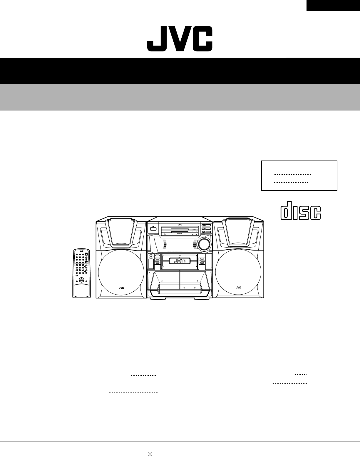
SERVICE MANUAL
COMPACT COMPONENT SYSTEM
MX-J300
J
C
MX-J300
Area Suffix
U.S.A.
Canada
RM-SMXJ300V REMOTE CONTROL
CLOCK TIMER POWER
1
2 3
–+
SELECT
SLEEP
4 5 6
SET
AUX
7 8 9
FM MODE
FM/AM
10+10
PLAY MODE
CD3CD2CD1
C D
/CLEAR
TAPE
A – TAPE - B
REC PAUSE
SHIFT
ACTIVE
SOUND
VOLUME
BASS EX.
MODE
Contents
Safety Precautions
Important for laser products
Preventing static electricity
Disassembly method
Adjustment method
COMPACT
CD
STANDBY
POWER
COMPACT
DIGITAL AUDIO
PLAY & EXCHANGER
1 BIT
DUAL D/A CONVERTER
PHONES
PANEL OPEN / CLOSE
TAPE
COMPU
AUX
PLAY
CONTROL
EJECT
PLAY
FULL - LOGIC CONTROL
1-2
1-3
1-4
1-5
1-24
MX-J300
POWERED ROLLING PANEL
AUTO REVERSE
Flow of functional operation
unit TOC read
Maintenance of laser pickup
Replacement of laser pickup
Description of major ICs
3
CD
2
CD
3
CD
2
CD
1
CD
1
VOLUME
+
–
CD
FM /AM
EJECT
REC/PLAY
DIGITAL AUDIO
1-27
1-28
1-28
1-29
COPYRIGHT 2000 VICTOR COMPANY OF JAPAN, LTD.
No.20818
Jul. 2000
Page 2
MX-J300
Safety Precautions
1. This design of this product contains special hardware and many circuits and components specially
for safety purposes. For continued protection, no changes should be made to the original design
unless authorized in writing by the manufacturer. Replacement parts must be identical to those
used in the original circuits. Services should be performed by qualified personnel only.
2. Alter ations of the design or circuitry of the product should not be made. Any design alterations of
the product should not be made. Any design alterations or additions will void the manufacturer`s
warranty and will further relieve the manufacture of responsibility for personal injury or proper ty
damage resulting therefrom.
3. Many electrical and mechanical par ts in the products have special safety-related characteristics.
These characteristics are often not evident from visual inspection nor can the protection afforded
by them necessarily be obtained by using replacement components rated for higher voltage,
wattage, etc. Replacement parts which have these special safety characteristics are identified in
the Parts List of Service Manual. Electrical components having such features are identified by
shading on the schematics and by ( ) on the Parts List in the Service Manual. The use of a
substitute replacement which does not have the same safety characteristics as the recommended
replacement parts shown in the Parts List of Service Manual may create shock, fire, or other
hazards.
4. The leads in the products are routed and dressed with ties, clamps, tubings, barriers and the
like to be separated from live parts, high temperature parts, moving parts and/or sharp edges
for the prevention of electric shock and fire hazard. When service is required, the or iginal lead
routing and dress should be observed, and it should be confirmed that they have been returned
to normal, after re-assembling.
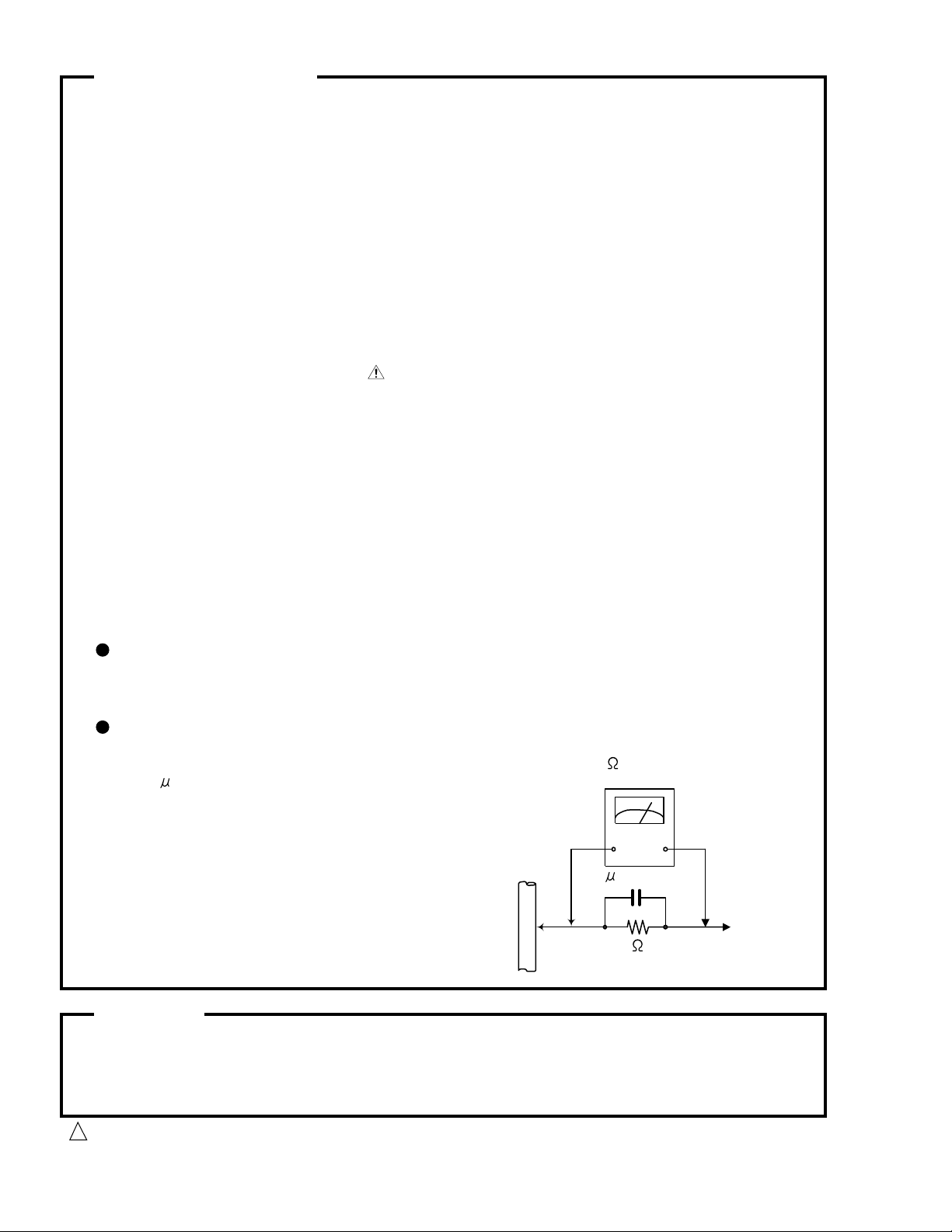
5. Leakage currnet check (Electrical shock hazard testing)
After re-assembling the product, always perform an isolation check on the exposed metal parts
of the product (antenna terminals, knobs, metal cabinet, screw heads, headphone jack, control
shafts, etc.) to be sure the product is safe to operate without danger of electrical shock.
Do not use a line isolation transformer during this check.
Plug the AC line cord directly into the AC outlet. Using a "Leakage Current Tester", measure
the leakage current from each exposed metal parts of the cabinet , particularly any exposed
metal part having a return path to the chassis, to a known good earth ground. Any leakage
current must not exceed 0.5mA AC (r.m.s.)
Alternate check method
Plug the AC line cord directly into the AC outlet. Use an AC voltmeter having, 1,000 ohms
per volt or more sensitivity in the following manner. Connect a 1,500 10W resistor paralleled by
a 0.15 F AC-type capacitor between an exposed
metal part and a known good earth ground.
Measure the AC voltage across the resistor with the
AC voltmeter.
Move the resistor connection to eachexposed metal
part, par ticularly any exposed metal part having a
return path to the chassis, and meausre the AC
voltage across the resistor. Now, reverse the plug in
the AC outlet and repeat each measurement. voltage
measured Any must not exceed 0.75 V AC (r.m.s.).
This corresponds to 0.5 mA AC (r.m.s.).
0.15 F AC TYPE
1500 10W
Good earth ground
AC VOLTMETER
(Having 1000
ohms/volts,
or more sensitivity)
Place this
probe on
each exposed
metal part.
Warning
1. This equipment has been designed and manufactured to meet international safety standards.
2. It is the legal responsibility of the repairer to ensure that these safety standards are maintained.
3. Repairs must be made in accordance with the relevant safety standards.
4. It is essential that safety critical components are replaced by approved parts.
5. If mains voltage selector is provided, check setting for local voltage.
Burrs formed during molding may be left over on some parts of the chassis. Therefore,
pay attention to such burrs in the case of preforming repair of this system.
1-2
CAUTION
!
Page 3
Important for laser products
MX-J300
1.CLASS 1 LASER PRODUCT
2.DANGER : Invisible laser radiation when open and inter
lock failed or defeated. Avoid direct exposure to beam.
3.CAUTION : There are no serviceable parts inside the
Laser Unit. Do not disassemble the Laser Unit. Replace
the complete Laser Unit if it malfunctions.
4.CAUTION : The compact disc player uses invisible
laserradiation and is equipped with safety switches
whichprevent emission of radiation when the drawer is
open and the safety interlocks have failed or are de
feated. It is dangerous to defeat the safety switches.
5.CAUTION : If safety switches malfunction, the laser is able
to function.
6.CAUTION : Use of controls, adjustments or performance of
procedures other than those specified herein may result in
hazardous radiation exposure.
CAUTION
!
Please use enough caution not to
see the beam directly or touch it
in case of an adjustment or operation
check.
1-3
Page 4
MX-J300
Preventing static electricity
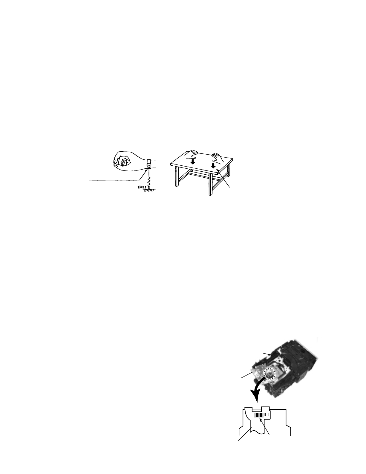
1. Grounding to prevent damage by static electricity
Electrostatic discharge (ESD), which occurs when static electricity stored in the body, fabric, etc. is discharged,
can destroy the laser diode in the traverse unit (optical pickup). Take care to prevent this when performing repairs.
2. About the earth processing for the destruction prevention by static electricity
In the equipment which uses optical pick-up (laser diode), optical pick-up is destroyed by the static electricity of
the work environment.
Be careful to use proper grounding in the area where repairs are being performed.
2-1 Ground the workbench
Ground the workbench by laying conductive material (such as a conductive sheet) or an iron plate over
it before placing the traverse unit (optical pickup) on it.
2-2 Ground yourself
Use an anti-static wrist strap to release any static electricity built up in your body.
(caption)
Anti-static wrist strap
Conductive material
(conductive sheet) or iron plate
3. Handling the optical pickup
1. In order to maintain quality during transport and before installation, both sides of the laser diode on the
replacement optical pickup are shorted. After replacement, return the shorted parts to their original condition.
(Refer to the text.)
2. Do not use a tester to check the condition of the laser diode in the optical pickup. The tester's internal power
source can easily destroy the laser diode.
4. Handling the traverse unit (optical pickup)
1. Do not subject the traverse unit (optical pickup) to strong shocks, as it is a sensitive, complex unit.
2. Cut off the shorted part of the flexible cable using nippers, etc. after replacing the optical pickup. For specific
details, refer to the replacement procedure in the text. Remove the anti-static pin when replacing the traverse
unit. Be careful not to take too long a time when attaching it to the connector.
3. Handle the flexible cable carefully as it may break when subjected to strong force.
4. It is not possible to adjust the semi-fixed resistor that adjusts the laser power. Do not turn it
Attention when traverse unit is decomposed
*Please refer to "Disassembly method" in the text for pick-up and how to
detach the CD traverse mechanism.
CD changer
mechanism
assembly
1. Remove the disk stopper and T. bracket on the CD changer mechanism
assembly.
2. Disconnect the harness from connector on the CD motor board.
3. CD traverse unit is put up as shown in Fig.1.
4. Solder is put up before the card wire is removed from connector CN601
on the CD servo control board as shown in Fig. 2.
(When the wire is removed without putting up solder, the CD pick-up
assembly might destroy.)
5. Please remove solder after connecting the card wire with CN601 when
you install picking up in the substrate.
1-4
CD traverse
unit
Flexible cable
Fig.1
Soldering
Fig.2
Page 5
MX-J300
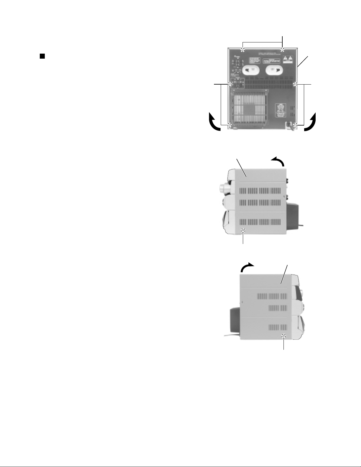
Remove the six screws A attaching the metal cover
on the back of the body.
Remove the two screws B on both sides of the body.
Remove the metal cover from the body while lifting
up the rear part of the metal cover.
1.
2.
3.
<Main body>
Removing the metal cover
(See Fig.1 to 3)
Disassembly method
Fig.3
Fig.2
Fig.1
Metal cover
A
A
A
Metal cover
B
Metal cover
B
1-5
Page 6
MX-J300
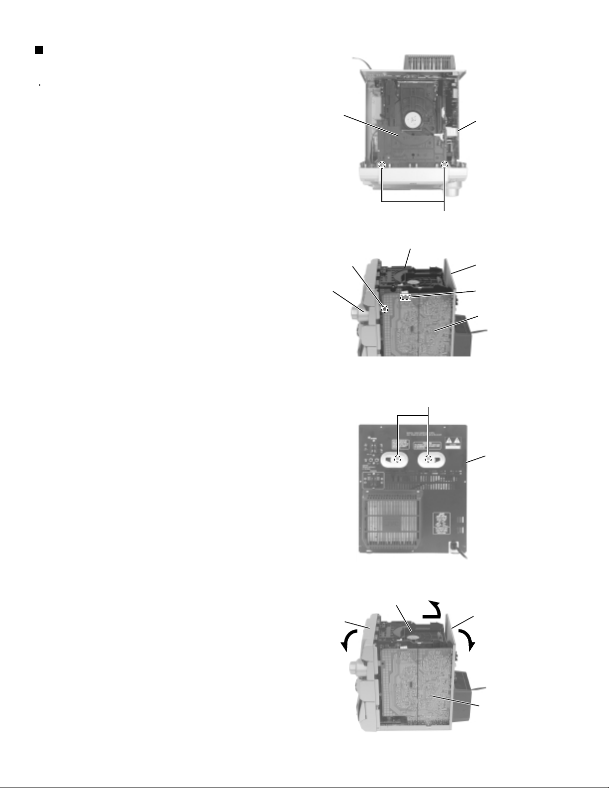
Removing the CD changer mechanism
assembly (See Fig.4 to 7)
Prior to performing the following procedures, remove
the metal cover.
1.
Remove the two screws C attaching the CD changer
mechanism assembly on the top of the body.
2.
Disconnect the card wire from connector CN303 on
top of the main board.
3.
Remove the plastic rivet a fixing the main board to
the front panel assembly on the left side of the body.
4.
Remove the two screws D from the rear panel.
5.
Detach upward the rear part of the CD changer
mechanism assembly while pulling the front panel
assembly and the rear panel outward, then pull out
the front part backward and upward.
CD changer
mechanism
assembly
Plastic rivet a
Front panel
assembly
C
Fig.4
CD changer mechanism assembly
Main board
CN303
Rear panel
CN303
CD changer mechanism
Front panel
assembly
Main board
Fig.5
D
Rear panel
Fig.6
assembly
Rear panel
1-6
Pull outward
Pull outward
Main board
Fig.7
Page 7
Prior to performing the following procedures, remove
the metal cover and the CD changer mechanism
assembly.
Disconnect the card wires from connector CN301,
CN304, CN305 and the harness from CN302 on the
inside of the main board.
Turn over the body and remove the two screws E.
Release the joint b on the bottom of the body and
the joints c and d on both sides of the body using a
screwdriver, and detach the front panel assembly
toward the front.
1.
2.
3.
Removing the front panel assembly
(See Fig.8 to 12)
Fig.10
Fig.9
Fig.8
Fig.11
Fig.12
Main board
Front panel
assembly
Main board
CN301
CN304
CN305
CN302
CN901A,CN901B
E
Front panel
assembly
Joint b
Front panel
assembly
Joint c
Front panel
assembly
Joint d
(Bottom)
MX-J300
1-7
Page 8
MX-J300
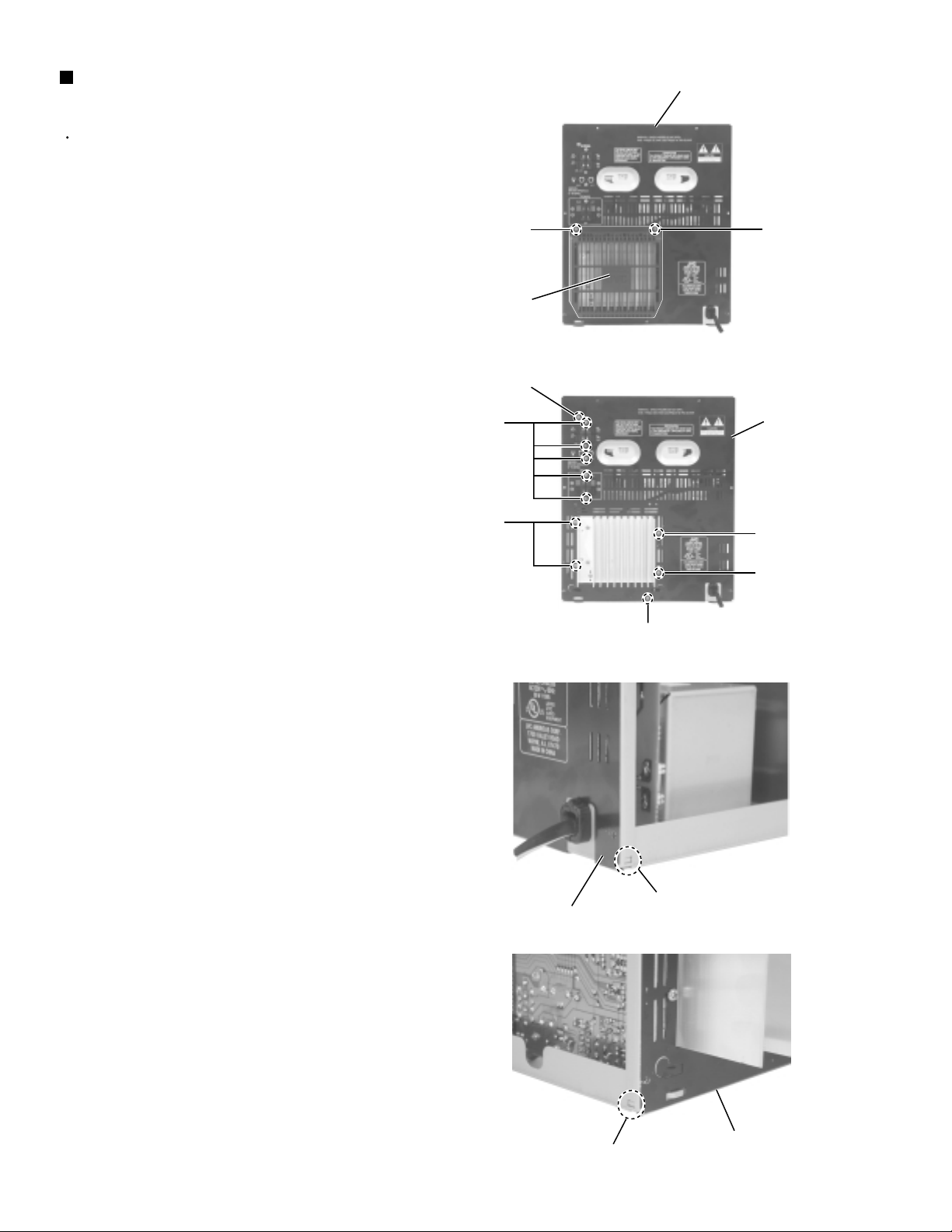
Removing the rear cover and the rear
panel (See Fig.13 to 16)
Prior to performing the following procedures, remove
the metal cover and the CD changer mechanism
assembly.
It is not necessary to remove the front panel
assembly.
1.
Remove the two screws F and the rear cover on the
back of the body.
2.
Remove the four screws G and the six screws H
attaching the main board and the heat sink to the
rear panel.
3.
Remove the screw I attaching the rear panel to the
base chassis.
4.
Release the lower two joints e and f on both sides of
the rear panel using a screwdriver and detach the
rear panel backwards.
Rear cover
G
H
G
Rear panel
FF
Fig.13
(To Earth bracket)
Rear panel
G
Rear panel
H
I
Fig.14
Joint e
Fig.15
1-8
Joint f
Rear panel
Fig.16
Page 9
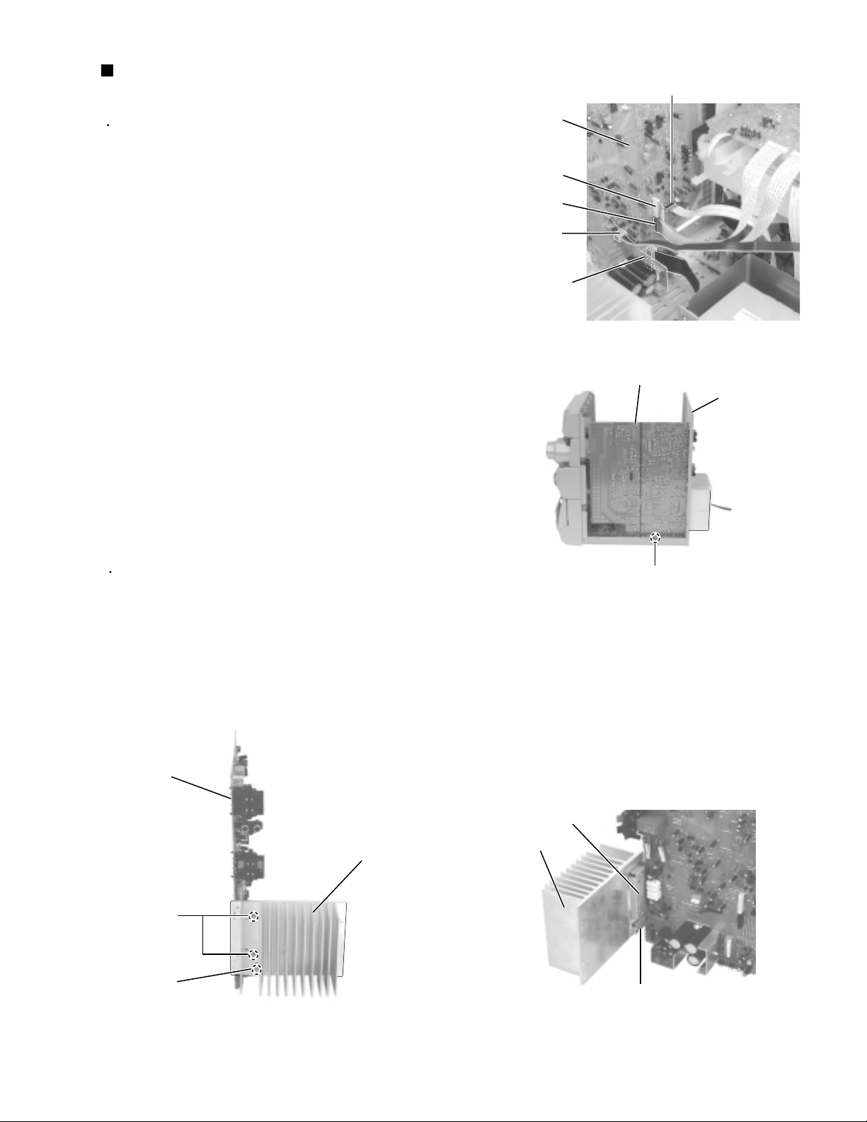
Prior to performing the following procedures, remove
the metal cover, the CD changer mechanism
assembly and the rear cover, rear panel.
It is not necessary to remove the front panel
assembly.
Disconnect the card wires from connector CN301,
CN304, CN305 and the harnesses from CN302,
CN901A and CN901B on the inside of the main
board.
From the right side of the body, remove the screw J
attaching the main board to the base chassis.
1.
2.
Removing the main board
(See Fig.17 to 20)
Prior to performing the following procedure, remove
the rear panel.
Remove the two screws K and the screw L attaching
the heat sink to the main board. Remove the IC
bracket 1 and 2 on the back of the heat sink.
Pull out the heat sink toward you.
1.
2.
~To remove the heat sink from
the main board~
Fig.17
Fig.18
J
Rear panel
Main board
Main board
CN301
CN304
CN305
CN302
CN901A,CN901B
Fig.19
Heat sink
K
L
Main board
Fig.20
Heat sink
IC bracket 2
IC bracket 1
MX-J300
1-9
Page 10
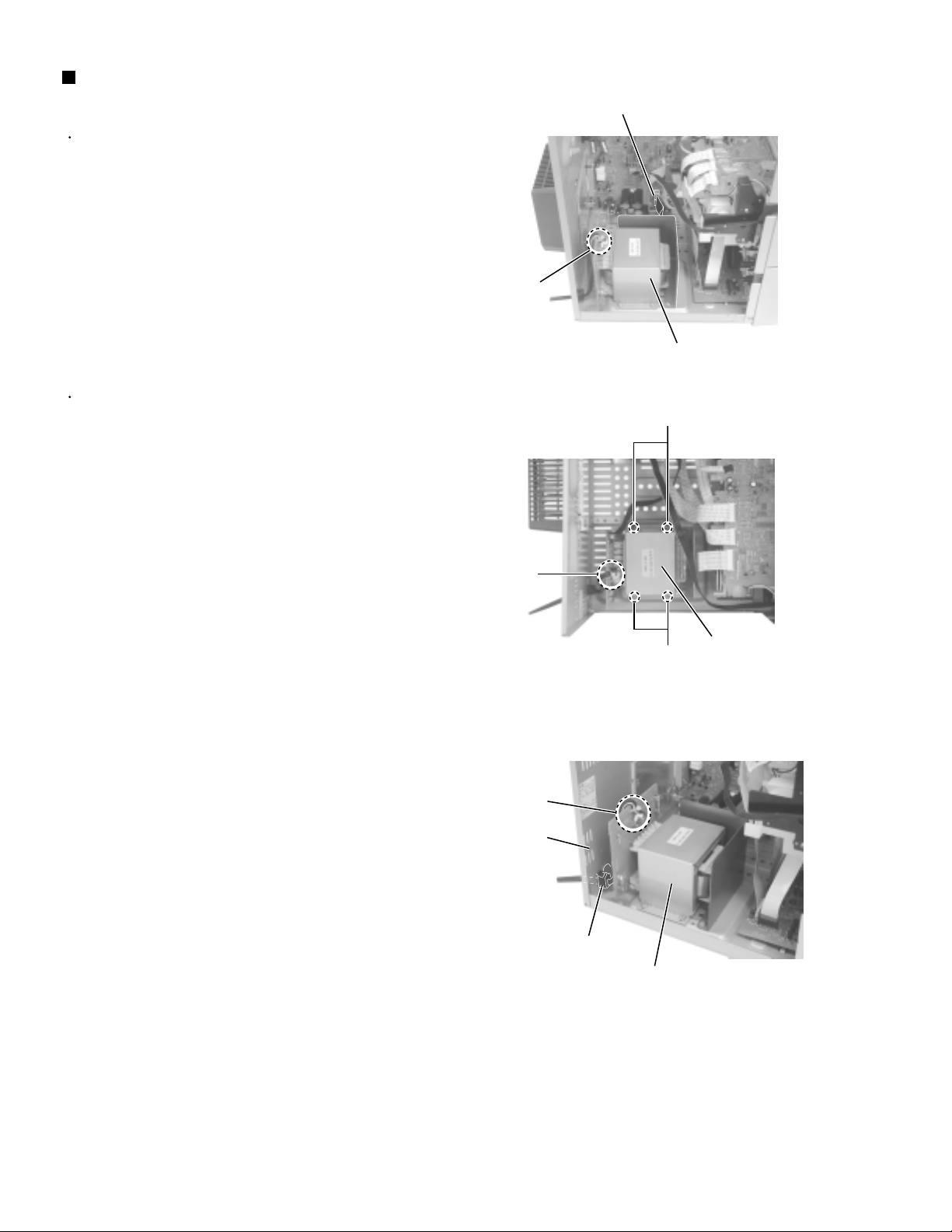
MX-J300
Removing the power transformer
assembly (See Fig.21 to 23)
Prior to performing the following procedure, remove
the metal cover and the CD changer mechanism
assembly.
1.
Disconnect the harness from connector CN901A and
CN901B on the inside of the main board.
2.
Cut off the tie band g of the power transformer
assembly and unsolder the power cord.
(Make sure to bundle the wires after repair.)
3.
Remove the four screws M attaching the power
transformer assembly.
When removing the power transformer assembly
with the power cord, remove the rear panel and pull
out the power cord stopper from the bottom chassis
upward.
CN901A,CN901B
Tie band g
Power transformer assembly
Fig.21
M
Tie band g
Tie band g
Rear panel
Power cord stopper
Power transformer
M
Fig.22
Power transformer
assembly
Fig.23
assembly
1-10
Page 11
Prior to performing the following procedure, remove
the metal cover, the CD changer mechanism
assembly and the front panel assembly.
Disconnect the card wire from connector CN352 on
the cassette amplifier board.
Remove the six screws N attaching the cassette
mechanism assembly.
Detach the cassette mechanism assembly toward
you.
1.
2.
3.
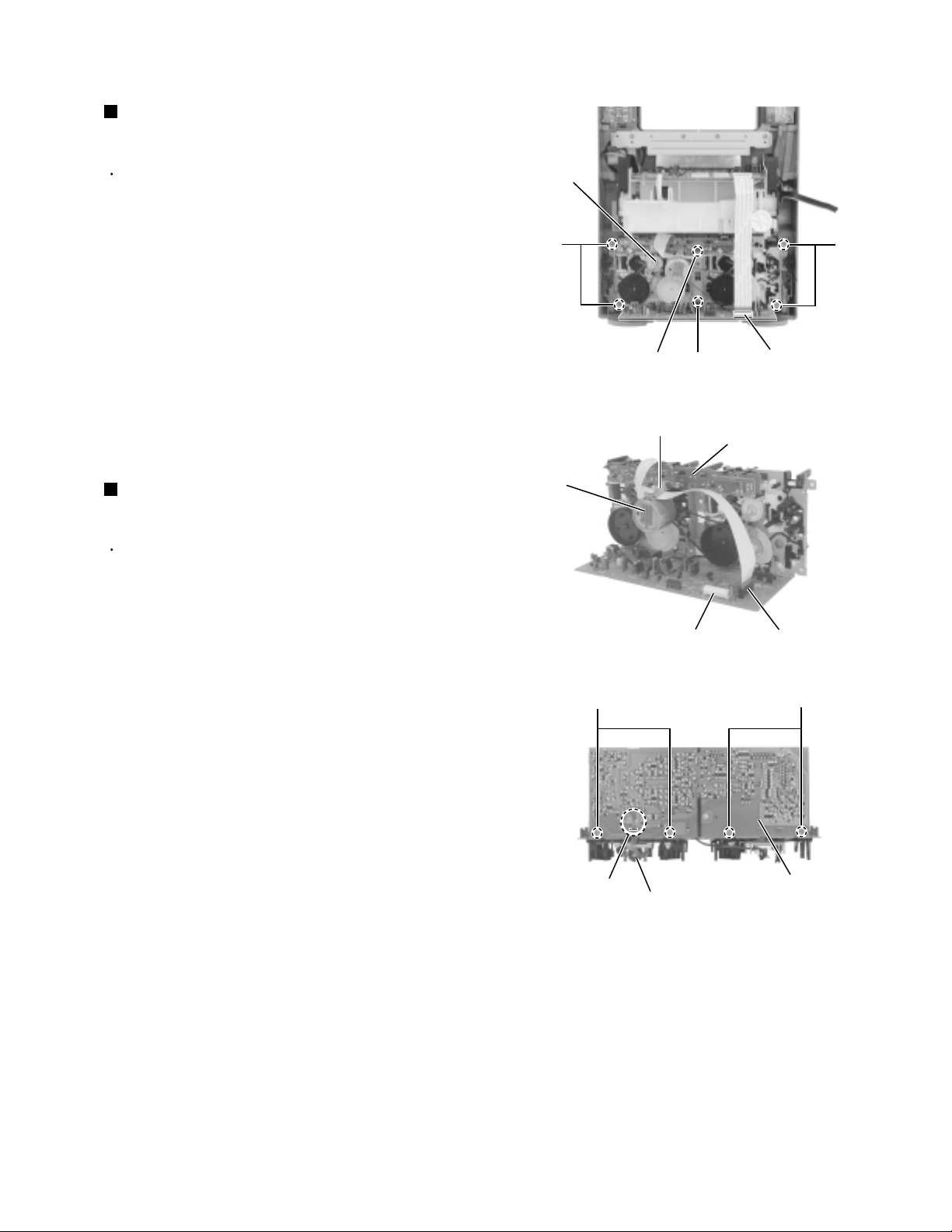
Prior to performing the following procedure, remove
the cassette mechanism assembly.
Disconnect the card wire from connector CN353 on
the cassette amplifier board.
1.
<Front panel assembly>
Removing the cassette mechanism
assembly (See Fig.24)
Removing the cassette amplifier board
(See Fig.25 and 26)
When reconnecting the card wire, put
it pass through under the harness h on
the DC motor (The Flg.27 shows the
details).
ATTENTION:
Unsolder the soldering i on the flexible wire for the
cassette amplifier board head at the bottom of the
cassette mechanism assembly.
Remove the four screws O attaching the cassette
amplifier board on the bottom of the cassette
mechanism assembly.
2.
3.
Fig.24
Fig.25
Fig.26
NN
N
O
O
N
Cassette
mechanism
assembly
Cassette amplifier board
CN352
Cassette amplifier board
Cassette amplifier board
CN352 CN353
Cassette mechanism
board
DC motor
h
Soldering i
R/P head
(Bottom)
MX-J300
1-11
Page 12
MX-J300
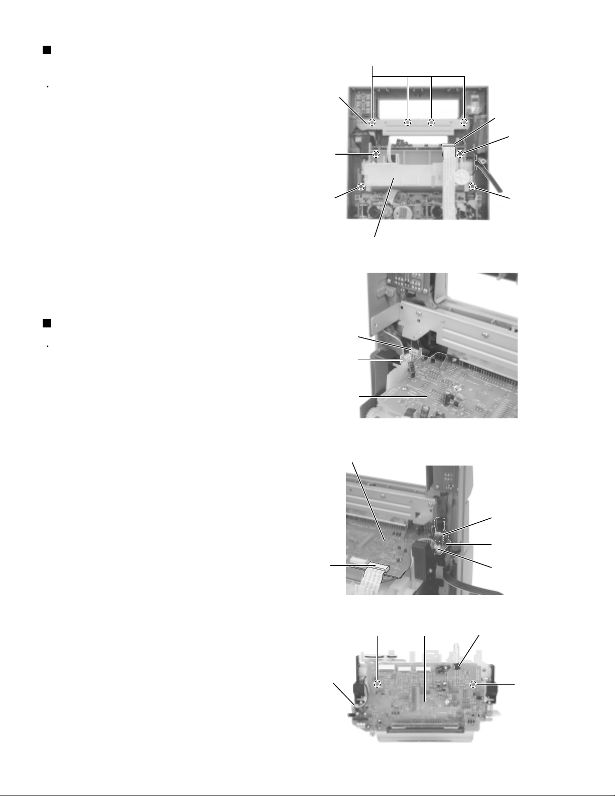
Removing the rolling panel assembly
(See Fig.27 to 29)
P
Prior to performing the following procedure, remove
the metal cover, the CD changer mechanism
assembly and the front panel assembly.
1.
Disconnect the card wire from connector CN704 and
the harness from CN706, CN707 and CN708 on the
display board over the rolling panel.
2.
Remove the four screws P attaching the bracket.
3.
Remove the four screws Q attaching the rolling panel
assembly.
4.
Pull out the rolling panel assembly.
Removing the display board (See Fig.30)
Prior to performing the following procedure, remove
the rolling panel assembly.
Bracket
Q
Q
Rolling panel assembly
CN707
CN706
Display board
Q
Q
Fig.27
1.
Disconnect the card wire from connector CN705 and
the harness from CN703 on the display board.
2.
Remove the two screws R attaching the display
board.
3.
Pull out the display board upward.
Display board
Display board
CN704
R
Fig.28
Fig.29
Display board
CN708
H.phone jack
board
CN703
CN705
1-12
CN703
R
Fig.30
Page 13

Prior to performing the following procedure, remove
the rolling panel assembly.
Pull out the volume knob on the front of the front
panel assembly and remove the nut attaching the
volume board.
Unhook the two hooks j on the back of the front
panel assembly and detach the volume board.
1.
2.
Remove the three screws T attaching the function
board 2.
Unsolder FW1004 on the function board 2 and
disconnect the harness extending from the eject
switch board.
1.
2.
Remove the two screws S attaching the function
board 1. Detach the function board downwards
while releasing it from the part k.
Unsolder FW1002 on the function board 1 and
disconnect the harness extending from the power
switch board.
1.
2.
Removing each board in the front panel
assembly (See Fig.31 to 33)
~Function board 1~ (Fig.31 and 33)
~Function board 2~ (Fig.31)
~Volume board~ (Fig.31 and 32)
Remove the screw W attaching the headphone
board.
1.
Remove the three screws V attaching the power
switch board.
Unsolder FW1002 on the power switch board and
disconnect the harness extending from the function
board 1.
1.
2.
Remove the four screws U attaching the eject switch
board.
Unsolder FW1004 on the eject switch board and
disconnect the harness extending from the function
board 2.
1.
2.
~Eject switch board ~ (Fig.33)
~Power switch board~ (Fig.31 and 33)
~Headphone board~ (Fig.33)
Fig.31
Fig.32
Fig.33
V
V
S
V
U
U
T
Power switch board
FW1002
Function board 1
(Tape / AWX)
Eject switch board
FW1004
Volume board
FW1002
Function board 2
(Audio / CD)
FW1004
Volume board
Hooks j
V
V
W
S
Function board 1
FW1002
Power switch board
FW1002
Headphone board
Part k
MX-J300
1-13
Page 14

MX-J300
<Rolling panel assembly>
Prior to performing the following procedures, remove
the metal cover the CD changer mechanism
assembly, the front panel assembly and the rolling
panel assembly.
It is not necessary to remove the display board.
Removing the multi control assembly
(See Fig.34 to 36)
1.
Remove the two screws X on both sides of the multi
control assembly.
2.
Disconnect the card wire from connector CN705 on
the display board.
3.
Pull outwards the joints l on both sides and detach
the multi control assembly toward the front.
Removing the multi control board
(See Fig.37 to 39)
Prior to performing the following procedure, remove
the multi control assembly.
Multi control assembly
Fig.34
X
Multi control assembly
1.
Remove the six screws Y attaching the cover and
the bracket.
2.
Release the hooks m on both sides of the panel
holder attaching the bracket and pull out the panel
holders outward.
Detach the multi control board with the cover and the
bracket attached.
3.
Remove the two screws Z attaching the multi control
board.
Hook m
Bracket
Panel holder
Fig.38
Multi control assembly
CN705
Bracket
Fig.35
X
Joint l
Fig.36
Y
Bracket
1-14
CN705
Multi control board
Z
Fig.39
Y
Y
Cover
Fig.37
Page 15

MX-J300
Prior to performing the following procedures, remove
the display board.
Remove the two screws A attaching the motor
bracket, then detach the motor leads from the fixing
plate n.
Remove the two screws B attaching the shaft
bracket.
Remove the motor belt.
Pull the parts o on each side of the shaft assembly
outwards and detach the shaft assembly upward.
Detach the drive motor assembly upward.
1.
2.
3.
4.
5.
Removing the drive motor assembly
(See Fig.40 to 41)
Fig.40
Fig.41
BA
Motor bracket
Shaft bracket
Fixing plate n
Shaft assembly Motor belt
Drive motor assembly
Part oPart o
1-15
Page 16

MX-J300
Removing the CD Servo control board
(See Fig.1)
1.Remove the metal cover.
2.Remove the CD changer mechanism assembly.
3.From bottom side the CD changer mechanism assembly,
remove the two screws A retaining the CD servo control
board.
4.Absorb the four soldered positions "a" of the right and
left motors with a soldering absorber.
5.Pull out the earth wire on the CD changer mechanism
assembly.
6.The two screws B is removed and C.B.holder is detached.
7.Disconnect the connector CN854 on the CD servo
control board.
8.Disconnect the card wire CN601 and the connector
CN801 on the CD servo control board.
A
a
a
CN854
A
CN651
CD servo control board
CN652
CN801
CN601
CN151
Removing the CD tray assembly
(See Fig.2~4)
Remove the front panel assembly.
1.
Remove the CD changer mechanism assembly.
2.
Remove the CD Servo control board.
3.
Remove the screw C retaining the lod stopper.
4.
From the T.bracket section "b" and clamper base
5.
section "c" , remove both of the edges fixing the
rod(See Fig.2 and 3).
Remove the screw D retaining the disc stopper
6.
(See Fig.3).
Remove the three screws E retaining the T.bracket
7.
(See Fig.3).
Remove the screw F retaining the clamper assembly
8.
(See Fig.3).
From the left side face of the chassis assembly, remove
9.
the one screw G retaining both of the return spring and
lock lever(See Fig. 4).
10.
By removing the pawl at the section "d" fixing the return
spring, dismount the return spring(See Fig.4).
11.
Remove the three lock levers(See Fig.4).
T.Braket
Disc stopper
D
Earth
wire
B
B
C.B.Holder
Fig.1
Clamper base
b
Rod
c
T.Braket
Fig.2
d
EE
C
a
Lod stopper
(C/J version only)
E
F
b
Lock lever
Fig.4
1-16
Clamper ass'y
Fig.3
Return spring
G
Page 17

MX-J300
11.
12.
Check whether the lifter unit stopper has been caught
into the hole at the section "e" of CD tray assembly as
shown in Fig.5.
Make sure that the driver unit elevator is positioned as
shown in Fig.6 from to the second or fifth hole on the
left side face of the CD changer mechanism assembly.
Fig.5
Fig.7
Fig.6
Fig.8
Fig.9
[Caution]
In case the driver unit elevator is not at above
position, set the elevator to the position as
shown in Fig.7 by manually turning the pulley
gear as shown in Fig.8.
13.
14.
15.
Manually turn the motor pulley in the clockwise
direction until the lifter unit stopper is lowered from the
section "e" of CD tray assembly(See Fig.8).
Pull out all of the three stages of CD tray assembly in
the arrow direction "f" until these stages stop
(See Fig.6).
At the position where the CD tray assembly has
stopped, pull out the CD tray assembly while pressing
the two pawls "g and g' " on the back side of CD tray
assembly(See Fig.9). In this case, it is easy to pull out
the assembly when it is pulled out first from the stage
CD tray assembly.
CD tray
assembly
e
Drive unit of elevator
CD tray assembly
f
Refer to Fig.7
Pawl
Chassis assembly
Pulley gear
Motor pulley
Pawl ,
CD tray assembly
Stopper
g
g
g'
1-17
Page 18

MX-J300
Removing the CD loading mechanism
assembly(See Fig.10)
1.2.While turning the cams R1 and R2 assembly in the
arrow direction "h" ,align the shaft "i" of the CD loading
mechanism assembly to the position shown in Fig.10.
Remove the four screws H retaining the CD loading
mechanism assembly.
Removing the CD traverse mechanism
(See Fig.11 and 12 )
For dismounting only the CD traverse mechanism
1.
without removing the CD loading mechanism assembly,
align the shaft "j" of the CD loading mechanism
assembly to the position shown Fig.11 while turning the
cam R1 and R2 assembly in the arrow direction "k" .
By raising the CD loading mechanism assembly in the
2.
arrow direction "l", remove the assembly from the lifter
unit
Cam R1, R2 assembly
Cams R1, R2 assembly
Arrow
h
i
H
H
CD loading mechanism assembly
Fig.10
H
H
CD traverse mechanism
Arrow
k
j
Fig.11
Removing the CD pick unit
(See Fig.13 )
1.
Move the cam gear in the arrow direction "m" . Then,
the CD pickup unit will be moved in the arrow direction
"n" .
According to the above step, shift the CD pickup unit to
2.
the center position.
While pressing the stopper retaining the shaft in the
3.
arrow direction "o" , pull out the shaft in the arrow
direction "p".
After dismounting the shaft from the CD pickup unit,
4.
remove the CD pickup unit
Lifter unit
o
Stopper
Shaft
Fig.12
CD Pickup unit
n
m
Shaft
p
Stopper
Fig.13
Arrow
CD loading
mechanism
Shaft
Cam gear
k
1-18
Page 19

Removing the cam unit
(See Fig.14 ~17 )
1.
Remove the CD loading mechanism assembly.
2.
While turning the cam gear "q", align the pawl "r"
position of the drive unit to the notch position(Fig.16) on
the cam gear "q".
Pull out the drive unit and cylinder gear(See Fig.17).
3.
While turning the cam gear "q", align the pawl "s"
4.
position of the select lever to the notch position(Fig.18)
on the cam gear "q".
Remove the four screws J retaining the cam unit(cam
5.
gear "q" and cams R1/R2 assembly)(See Fig.18).
MX-J300
Chassis assembly
CN801
CN802
Fig.14
Drive unit
Tray select
switch board
Cylinder gear
CN804
Drive unit
r
I
Cam gear q
Cam gear q
Fig.15
J
Cams R1, R2 assembly
Cam unit
Fig.16
J
J
s
Select lever
Fig.17
1-19
Page 20

MX-J300
Removing the actuator motor and belt
(See Fig.18~21)
1.
Remove the two screws K retaining the gear bracket
(See Fig.19).
2.
While pressing the pawl "t" fixing the gear bracket in the
arrow direction, remove the gear bracket
(See Fig.19).
From the notch "u section" on the chassis assembly
3.
fixing the edge of gear bracket, remove and take out the
gear bracket(See Fig. 20).
Remove the belts respectively from the right and left
4.
actuator motor pulleys and pulley gears(See Fig. 19).
After turning over the chassis assembly, remove the
5.
actuator motor while spreading the four pawls "v" fixing
the right and left actuator motors in the arrow
direction(See Fig. 21).
[Note]
When the chassis assembly is turned over under
the conditions wherein the gear bracket and belt
have been removed, then the pulley gear as well
as the gear, etc. constituting the gear unit can
possibly be separated to pieces. In such a case,
assemble these parts by referring to the assembly
and configuration diagram in Fig. 22.
Chassis assembly
Pulley gear
Gear bracket
Belt
Motor pulley
K
Fig.18
Actuator motor
Pulley gear
Belt
Motor pulley
K
Pawl
t
u
Gear bracket
Fig.19
Assembly and Configuration Diagram
Pulley gear
Gear B
v
v
Fig.20
Pulley gear
Gear B
Cylinder gear
1-20
Gear C
Select gear
Gross gear L
Fig.21
Gross gear U
Gear C
Page 21

MX-J300
Fig.22
[Caution]
To reassemble the cylinder gear, etc.with the
cam unit (cam gear and cans R1/R2 assembly),
gear unit and drive unit, align the position of the
pawl "x" on the drive unit to that of the notch on
the cam gear "q". Then, make sure that the
gear unit is engaged by turning the cam gear
"q" (See Fig. 24).
Removing the cams R1/R2 assembly
and cam gear q(See Fig.22)
1.
2.
3.
4.
Remove the slit washer fixing the cams R1 and R2
assembly.
By removing the two pawls "w" fixing the cam R1,
separate R2 from R1.
Remove the slit washer fixing the cam gear "q".
Pull out the cam gear "q" from the C.G. base assembly.
Removing the C.G. base assembly
(See Fig.22 and 23)
Remove the three screws L retaining the C.G. base
assembly.
Fig.23
Slit washer
Pawl
Cam R2
Slit washer
Cam gear L
Cam switch board
C.G. base assembly
Cam R1
Pawl
Cam gear L
Notch
Cylinder
gear
Gear bracket
Cam R1, R2 assembly
Gear unit
Drive unit
x
Pawl
w
w
L
1-21
Page 22

MX-J300
< Cassette mechanism section >
Removing the R/P head assembly
(See Fig.1to2)
1.
Unsolder the head wire from the cassette
mechanism board.
2.
Remove the two screws A retaining the R/P head
assembly.
Refer to the figure for soldering
Cassette mechanism board
Sold part
Fig.2
Removing the R/B head assembly
(See Fig.3)
A
A
R/P head assembly
Fig.1
1.
Loosen the screw B attaching the P/B head.
2.
Remove the screws C retaining the R/B head
assembly.
Removing the Pinch roller assembly
(See Fig.4)
1.
Pull the tab a outward and remove the pinch roller
upward.
B
C
Fig.3
Tab a
1-22
Pinch roller
Fig.4
Page 23

Remove the two screws D attaching the capstan
motor.
Unsolder the motor wire.
1.
2.
Removing the Capstan motor
(See Fig.5 to 7)
Remove the capstan motor.
Remove the capstan belt.
ATTENTION: Do not stain the belt with grease.
1.
2.
Removing the Capstan belt (See Fig.7)
Fig.5
Fig.6
Fig.7
Cassette mechanism assembly
FR belt
D
Capstan motor
Sold part
FR belt
Capstan belt
Marke red line
Motor wire
Capstan motor
Un solder
MX-J300
1-23
Page 24

MX-J300
Adjustment method
Measurement instruments required
for adjustment
1. Low frequency oscillator,
This oscillator should have a capacity to output 0dBs
to 600ohm at an oscillation frequency of 50Hz-20kHz.
2. Attenuator impedance : 600ohm
3. Electronic voltmeter
4. Frequency counter
5. Wow flutter meter
6. Test tape
VT712
VT703
characteristics(1kHz),and dubbing frequency
characteristics(63,1,10kHz)
Because of frequency-mixed tape with 63,1k,10k and
14kHz(250nWb/m -24dB).
Use this tape together with a filter.
7. Blank tape
TAPE : AC-225, TAPE : AC-514
8. Torque gauge : For play and back tension
Forward ; TW2111A, Reverse ; TW2121A
Fast Forward and Rewind ; TW2231A
9. Test disc
: CTS-1000(12cm),GRG-1211(8cm)
10. Jitter meter
Measurement conditions
Power supply voltage
AC120V(60Hz)
Measurement
output terminal : Speaker out
:TP101(Mesuring for TUNER/DECK/CD)
:Dummy load 6ohm
: For Tape speed and wow flutter ( 3kHz)
: For Head angle(10kHz),Play back frequency
Radio input signal
AM modulation frequency : 400Hz
Modulation factor : 30%
FM modulation frequency : 400Hz
Frequency displacement : 22.5kHz
Frequency Range
AM 531kHz~1710kHz
FM 87.5MHz~108MHz
Standard measurement positions of volume
and switch
Power : Standby (Light STANDBY Indicator)
S,A,BASS : OFF
Sound mode : OFF
Main VOL. : 0 Minimum
Travers mecha set position : Disc 1
Precautions for measurement
1. Apply 30pF and 33kohm to the IF sweeper output
side and 0.082 F and 100kohm in series to
the sweeper input side.
2. The IF sweeper output level should be made as
low as possible within the adjustable range.
3. Since the IF sweeper is a fixed device, there is
no need to adjust this sweeper.
4. Since a ceramic oscillator is used, there is no need
to perform any MPX adjustment.
5. Since a fixed coil is used, there is no need to adjust
the FM tracking.
6. The input and output earth systems are separated.
In case of simultaneously measuring the voltage
in both of the input and output systems with an
electronic voltmeter for two channels, therefore,
the earth should be connected particularly.
7. In the case of BTL connection amplifier, the minus
terminal of speaker is not for earthing. Therefore,
be sure not to connect any other earth terminal
to this terminal. This system is of an OTL system.
1-24
Page 25

Arrangement of adjusting positions
Cassette mechanism section (Mechanism A section)
Cassette mechanism section (Back side)
Head azimuth
adjusting screw
(Forward side)
Head azimuth
adjusting screw
(Reverse side)
Head azimuth
adjusting screw
(Forward side)
Head azimuth
adjusting screw
(Reverse side)
Playback
head
Playback,recording and eraser
heads or playback head
1.Playback the test tape VT703(10kHz).
2.With the playback mechanism or recording &
playback mechanism, adjust the head azimuth
screw so that the forward and reverse output
levels become maximum.After adjustment,lock
the head azimuth at least by half a turn.
3.In either case,this adjustment should be
performed in both the forward and reverse
directions with the head azimuth screw.
<Constant speed>
Adjust the volume inside of capstan motor1 so that
the frequency counter reading becomes 3,000Hz
60Hz when playing back the test tape VT712(3kHz)
with the playback mechanism or playback and
recording mechanism after ending forward winding
of the tape.
Confirmation
of head angle
Confirmation
of tape speed
Test tape
VT703(10kHz)
Measurement
output terminal
:Speaker terminal
Speaker R
(Load resistor:3ohm)
:Headphone terminal
Test tape
:VT712(3kHz)
Measurement
output terminal
:Headphone terminal
Maximum
output
Tape speed
of decks
(A and B)
:3,000Hz
60Hz
Adjust the head
azimuth screw
only when the
head has been
changed.
Volume Inside
of capstan
motor
Items Measurement
conditions
Measurement method
Standard
values
Adjusting
positions
Tape recorder section
MX-J300
1-25
Page 26

MX-J300
Reference values for confirmation items
Items Measurement
Double tape
speed
conditions
Test tape
:VT703(10kHz)
Measurement
output terminal
:Speaker terminal
Speaker R
(Load resistance:3ohm)
measurement
output terminal
:Headphone terminal
After setting to the double speed motor, confirm
that the frequency counter reading becomes
4,800+400/-300Hz when the test tape VT712
(3kHz) has been play back with the playback
mechanism.
Measurement method
Standard
values
4,800+400/
-300Hz
Adjusting
positions
Playback
mechanism side
Difference
between the
forward and
reverse speed.
P.mecha and
R/P mecha
speed
Wow & flutter
Test tape
:VT703(10kHz)
Measurement
output terminal
:Headphone terminal
When the test tape VT712(3kHz) has been played
back with the playback mechanism or recording and
playback mechanism at the beginning of forward
winding, the frequency counter reading of the
difference between both of the mechanisms should
be 6.0Hz or less.
When the test tape VT712(3kHz) has been played
back with the playback mechanism or recording and
playback mechanism at the beginning of forward
winding the frequency counter reading of wow &
flutter should be 0.25% or less(WRMS).
Reference values for electrical function confirmation items
Items Measurement
Recording
bias frequency
conditions
*Recording and
playback side forward
or reverse
*Test tape
:TYP AC-514
*Measurement
terminal BIAS TP on
P.C.board
1.While changing over to and from BIAS 1 and 2,
confirm that the frequency is changed.
2.With the recording and playback mechanism.
load the test tape (AC-514 to TYP ),and set the
mechanism to the recording and pausing
conditions in advance.
3.Confirm that the BIAS TP frequency on the
P.C.board is 100kHz 6kHz.
Measurement method
60Hz or
less
with in
0.25%
JIS(WTD)
Standard
values
100kHz
+9kHz
-7kHz
Both the playback
and recording &
playback
mechanism
Both the playback
and recording &
playback
mechanism
Adjusting
positions
Eraser current
(Reference
value)
1-26
*Recording and
playback side forward
or reverse
*Recording mode
*Test tape
:AC-514 and AC-225
Measurement terminal
Both of the eraser
head
1.With the recording and playback mechanism,
load the test tapes(AC-514 to TYP and AC-225
to TYP ),and set the mechanism to the recording
and pausing condition in advance.
2.After setting to the recording conditions, connect
1Mohm in series to the eraser head on the
recording and playback mechanism side, and
measure the eraser current from both of the eraser
terminal.
TYP
:120mA
TYP
:75mA
Page 27

Flow of functional operation until TOC read
Power ON
Play Key
Slider turns REST
SW ON.
Automatic tuning
of TE offset
Confirm that the voltage at the pin5
of CN801 is "H"\"L"\"H".
MX-J300
Check Point
Tracking error waveform at TOC reading
Approx.3sec
Tracking
servo
off states
Automatic measurement
of TE amplitude and
automatic tuning of
TE balance
VREF
pin 25 of
IC601(TE)
Approx
1.8V
Disc states
to rotate
Tracking
servo
on states
Disc to be
braked to stop
TOC reading
finishes
500mv/div
2ms/div
Fig.1
Laser ON
Detection of disc
Automatic tuning of
Focus offset
Automatic measurement of
Focus S-curve amplitude
Disc is rotated
Focus servo ON
(Tracking servo ON)
Automatic measurement of
Tracking error amplitude
Automatic tuning of
Tracking error balance
Check that the voltage at the
pin40 of IC651 is + 5V?
Confirm that the Focus error
S-cuve signal at the pin28 of
IC651 is approx.2Vp-p
Confirm that the signal from
pin24 IC651 is 0V as a
accelerated pulse during
approx.400ms.
Confirm the waveform of
the Tracking error signal.
at the pin 25 of IC601 (R604)
(See fig-1)
Automatic tuning of
Focus error balance
Automatic tuning of
Focus error gain
Automatic tuning of
Tracking error gain
TOC reading
Play a disc
Confirm the eys-pattern
at the lead of TP1
1-27
Page 28

MX-J300
Maintenance of laser pickup
(1) Cleaning the pick up lens
Before you replace the pick up, please try to
clean the lens with a alcohol soaked cotton
swab.
(2) Life of the laser diode
When the life of the laser diode has expired,
the following symptoms will appear.
1. The level of RF output (EFM output:ampli
tude of eye pattern) will below.
Is the level of
RFOUT under
1.25V 0.22Vp-p?
YES
O.K
NO
Replace it.
Replacement of laser pickup
Turn off the power switch and,disconnect the
power cord from the AC outlet.
Replace the pickup with a normal one.(Refer
to "Pickup Removal" on the previous page)
Plug the power cord in,and turn the power on.
At this time,check that the laser emits for
about 3seconds and the objective lens moves
up and down.
Note: Do not observe the laser beam directly.
Play a disc.
Check the eye-pattern at TP1.
Finish.
(3) Semi-fixed resistor on the APC PC board The semi-fixed resistor on the APC printed circuit board which is
attached to the pickup is used to adjust the laser power.Since this adjustment should be performed to match the
characteristics of the whole optical block, do not touch the semi-fixed resistor.
If the laser power is lower than the specified value,the laser diode is almost worn out, and the laser pickup should
be replaced.
If the semi-fixed resistor is adjusted while the pickup is functioning normally,the laser pickup may be damaged
due to excessive current.
1-28
Page 29

Description of major ICs
BA6897FP-W(IC801): 4channel driver
1.Pin layout & Block diagram
GND
CH4-OUTA
CH4-OUTB
CH4-INA
CH4-INB
BIAS IN
28 27 26 25 24 23 22
10K
D.BUF
D.BUF
T.S.D
13.3K
Level shift
10K
10K
Vcc
REGULATOR
Vcc
Vcc
CH3-INB
CH3-INA
CH3-OUTB
CH3-OUTA
21 20 19 18 17 16 15
Vcc
50K
50K
10K
D.BUF
13.3K
Level shift
DRIVER MUTE
OP IN(+)
OP IN(-)
D.BUF
MX-J300
D.BUF
1 2 3 4 5 6 7
CH1-OUTA
2.Pin function
Pin
Symbol
NO.
1
CH1-OUTA
2
CH1-OUTB
3
CH1-INA
4
CH1-INB
5
Tr-B
6
Vreg OUT
7
MUTE
8
GND
9
CH2-INB
10
CH2-INA
11
CH2-OUTB
12
CH2-OUTA
13
GND
14
OPOUT
Level shift
10K
D.BUF
CH1-INA
13.3K
Tr-B
Vreg
CH1-INB
OUT
MUTE
CH1-OUTB
Function
Driver CH1 - output
Driver CH1 + output
Driver CH1 input
Driver CH1 gain adjustment Input terminal
Connect to the base of external Tr
Fixed voltage output
Mute control terminal
GND
Driver CH2 gain adjustment Input terminal
Driver CH2 input
Driver CH2 + output
Driver CH2 - output
Sub-slate GND
Operation amplifier output
13.3K
10K
8 9 10 11 12 13 14
Level shift
D.B U F
GND
CH2-INB
CH2-INA
CH2-OUTA
CH2-OUTB
Pin
NO.
15
16
17
18
19
20
21
22
23
24
25
26
27
28
Symbol
OP IN(-)
OP IN(+)
CH3-OUTA
CH3-OUTB
CH3-INA
CH3-INB
Vcc
Vcc
BAIS IN
CH4-INB
CH4-INA
CH4-OUTB
CH4-OUTA
GND
Operation amplifier - input
Operation amplifier + output
Driver CH3 - output
Driver CH3 + output
Driver CH3 input
Driver CH3 gain adjustment Input terminal
Pow er supply terminal
Pow er supply terminal
Bias amplifier input terminal
Driver CH4 gain adjustment Input terminal
Driver CH4 input
Driver CH4 + output
Driver CH4 - output
Sub-slate GND
Function
D.B U F
GND
OP-OUT
T.S.D;Thermal shutdown
D.BUF:Drive buffer
1-29
Page 30

MX-J300
AN8806SB-W (IC601) : RF&Servo AMP
1.Pin layout
PD
LD
LDON
LDP
VCC
RF-
RF OUT
RF IN
C.AGC
ARF
C.ENV
C.EA
CS BDO
BDO
CS BRT
OFTR
/NRFDET
GND
2.Block diagram
1
2
3
4
5
6
7
8
9
10
11
12
13
14
15
16
17
18
36
35
34
33
32
31
30
29
28
27
26
25
24
23
22
21
20
19
PDAC
PDBD
PDF
PDE
PDER
PDFR
TBAL
FBAL
EF EF OUT
TE TE OUT
CROSS
TE BPF
VDET
LD OFF
VREF
ENV
6
36
-+
35
-+
31
34
--
728
-+
+
VCBA
--
+
VCBA
--
--
VCBA
+
29
--
+
-+
27
-+
910 17
8
AGC
EQ
OFTR
RF
DET
BDO
11
12 19
ENV CURCUIT
13
14
15
16
-+
20
+
+
32
33
-+
--
VCBA
+
+
--
-+
--
--
+
+
--
21
2
+
--
1-30
24 25
30
23
26
22
14
3
Page 31

35
36
34
33
32
31
30
29
28
27
26
25
24
23
22
21
20
19
18
17
16
15
14
13
12
11
10
9
8
7
6
5
4
3
2
1
3. Pin function
PD AC
FBAL
TBAL
PDFR
PDER
PDF
PDE
PD BD
TE BPF
VDET
CROSS
TE OUT
TE-
FE OUT
FE-
/NRFDET
GND
LD OFF
VREF
ENV
OFTR
C.AGC
ARF
C.ENV
C.EA
CS BDO
BDO
CS BRT
LD
LD ON
LDP
VCC
RF-
RF OUT
RF IN
PD
Pin No.
Symbol
I/O
I
O
I
--
-I
O
I
I/O
O
I/O
I/O
I/O
O
I/O
O
O
-O
O
-O
I
O
O
I
O
I
I
I
I/O
I/O
I
I
I
I I-V amp input
I-V amp input
I-V amp input
I-V amp input
E I-V amp gain control
F I-V amp gain control
Tracking balance control
Focus balance control
Inverse input pin for focus error amp
Output pin of focus error
Inverse input pin for tracking error amp
Tracking error signal output
Tracking error cross output
Input pin of tracking error through BPF
Vibration detection signal output
Connect to ground
Reference voltage output
Description
APC amp input terminal
APC amp output terminal
APC ON/OFF control terminal
Envelope output
Ground
RF detection signal output
Of-track status signal output
BDO output pin
A capacitor is connected to this terminal to detect the envelope of RF signal
RF output
Connecting pin of AGC loop filter
RF input
RFamp output
Inverse input pin for RF amp
Power supply
Connect to ground
A capacitor is connected to this terminal to detect the envelope of RF signal
A capacitor is connected to detect the lower envelope of RF signal
A capacitor is connected to detect the lower envelope of RF signal
MX-J300
1-31
Page 32

MX-J300
BA15218F(IC303):OP AMP.
1OUT1
2-IN1
-
8
7
VCC
OUT2
1
3+IN1
+
-
-IN2
6
2
EE
4
+
5V
+IN2
BA3126N(IC31) : R/P Switch
S W
R E C
G
123456789
P / B
S W
C O N T .
G N D
V c c
P / B
G
S W
S W
R E C
TA8409S(IC851,IC852):Motor driver
1.Pin layout 2.Pin function
1
IN2
VCC
OUT 2
GND
GND
VS
OUT 1
VR
IN1
2
3
4
5
6
7
8
9
TA8409S
INPUT OUTPUT MODE
IN1
IN2
0
0
1
0
0
1
1
1
OUT1
H
L
L
OUT2
L
H
L
MOTOR
STOP
CW/CCW
CCW/CW
BRAKE
1-32
Page 33

LC72136N (IC2) : PLL Frequency synthesizer
1. Pin layout
FM/AM
CLOCK
FM/ST/VCO
AM/FM
2. Block
XT
CE
DI
DO
SDIN
1
2
3
4
5
6
7
8
9
10
11
22
21
20
19
18
17
16
15
14
13
12
XT
GND
LPFOUT
LPFIN
PD
VCC
FMIN
AMIN
IFCONT
IFIN
MX-J300
3. Function
Pin
Symbol
No.
1
FM/AM
2
3
4
CLOCK
5
6
FM/ST/VCO
7
AM/FM
8
9
10
11
1
22
16
15
3
4
5
6
17
21
XT
CE
DI
DO
LW
MW
SDIN
Reference
Driver
Swallow Counter
1/2
C
2B
I/F
Power
on
Reset
Function
I/O
X'tal oscillator connect (75kHz)
I
LOW:FM mode
O
When data output/input for 4pin(input) and
I
Swallow Counter
1/16,1/17 4bit
1/16,1/17 4bit
12bit
Programmable
DriverS
Data Shift Register & Latch
7821113
6pin(output): H
Input for receive the serial data from
I
controller
Sync signal input use
I
Data output for Controller
O
Output port
"Low": MW mode
O
Open state after the power on reset
O
Input/output port
I/O
Input/output port
I/O
Data input/output
I/O
Phase
Detector
Charge Pump
Unlock
Detector
Universal
Counter
Pin
No.
12
13
14
15
16
17
18
19
20
21
22
Symbol
IFIN
IFCONT
AMIN
FMIN
VCC
PD
LPFIN
LPFOUT
GND
XT
18
19
20
12
I/O
Function
IF counter signal input
I
IF signal output
O
Not use
-
AM Local OSC signal output
I
FM Local OSC signal input
I
Power suplly(VDD=4.5-5.5V)
When power ON:Reset circuit move
PLL charge pump output(H: Local OSC
O
frequency Height than Reference frequency.
L: Low Agreement: Height impedance)
Input for active lowpassfilter of PLL
I
Output for active lowpassfilter of PLL
O
Connected to GND
X'tal oscillator(75KHz)
I
1-33
Page 34

MX-J300
MN35510 (IC651) : DIGITAL SERVO&DIGITAL SIGNAL PROCESSER
1. Terminal Layout
2.Block Diagram
LRCKIN(MSEL)
BCLK(SSEL)
SRDATAIN
(PSEL)
IOSEL
CLVS
CRC
BLKCK
CLDCK
SBCK
SUBC
DEMPH
RESY
FLAG6(RESY)
SSEL
SQCK
SUBQ
AVDD2
AVDD2
PCK
EFM
PLLF
DSLF
IREF
DRF
ARF
RSEL
PSEL
MLD
MCLK
MDATA
CK384(EFM)
VCOF
BYTCK
SMCK
FCLK
CSEL
MSEL
X2
X1
ÊSTAT
DIGITAL
DEEMPHSIS
SUB
CODE
BUFFER
DSL.
PLL
VCO
VCO
ITUNING
GENERATION
PITCH
CONTROL
20 ~ 1
21
~
40
41 ~ 60
8TIMES
OVER SAMPUNC
DIGITAL FILTER
EFM
DEMODULATION
SYNC
INTERPOLATION
SUBCODE
DEMODULATION
MICRO
COMPUTER
INTERFACE
A/D
COVERTER
80
~
61
1BIT
DAC
LOGIC
S
16k
SRAM
CIRC
ERROR
CORRECTION
DEINTERLEVE
CLV
SERVO
INPUT
PEM
(R)
PEM
(L)
D/A
CONVERTER
OUTPUT
DIGITAL
AUDIO
INTERFASE
DIGITAL
AUDIO
INTERFASE
INTER POLATION
SOFT MUTING DIGITAL
ATTENUATION
PEAK DETECTIVE
AUTO CUE
PORT
SERVO
TIMING GENERATOR
AVSS1
AVDD1
OUTR
OUTL
FLAG
IPFLAG
TX
ECM
PC
LRCK
SRDATA
BCLK
DMUTE
TRKV
KICK
VREF
TRVSTR
ECS
TVD
TRD
FOD
TBAL
FBAL
TOFS
TES
/TLOCK
/FLOCK
PLAY
LDON
WVEL
SENSE
1-34
D
/
D
V
V
V
S
D
D
S
D
D
1
/
R
V
T
S
S
E
T
S
S
1
T
F
E
R
T
F
E
E
N
V
T
R
C
R
S
B
V
D
D
O
E
T
/
R
F
D
E
O
F
T
Page 35

3. Description
Pin
No.
1
2
3
4
5
6
7
8
9
10
11
12
13
14
15
16
17
18
19
20
21
22
23
24
25
26
27
28
29
30
31
32
33
34
35
36
37
38
39
40
symbol
BCLK
LRCK
SRDATA
DVDD1
DVSS1
TX
MCLK
MDATA
MLD
SENSE
FLOCK
TLOCK
BLKCK
SQCK
SUBQ
DMUTE
STATUS
RST
SMCK
PMCK
TRV
TVD
PC
ECM
ECS
KICK
TRD
FOD
VREF
FBAL
TBAL
FE
TE
RF ENV
VDET
OFT
TRCRS
RFDET
BDO
LDON
I/O
O
O
O
O
O
O
Description
Not used
Not used
Not used
I
Power supply (Digital)
I
Connected to GND
Digital audio interface output
com command clock signal input
I
(Data is latched at signal's rising point)
com command data input
I
I
com command load signal input
Not used
O
Not used
Not used
sub-code block clock signal output
O
I
Outside clock for sub-code Q resister input
Sub-code Q -code output
O
I
Connected to GND
Status signal
O
(CRC,CUE,CLVS,TTSTOP,ECLV,SQOK)
Reset signal input (L:Reset)
I
I
Not used
I
Not used
O
Traverse enforced output
O
Traverse drive output
I
Not used
Spindle motor drive signal (Enforced
O
mode output) 3-State
Spindle motor drive signal (Servo error
O
signal output)
Kick pulse output
O
Tracking drive output
O
O
Focus drive output
Reference voltage input pin for D/A
I
output block (TVD,FOD,FBA,TBAL)
Focus Balance adjust signal output
O
O
Tracking Balance adjust signal output
Focus error signal input(Analog input)
I
Tracking error signal input(Analog input)
I
I
RF envelope signal input(Analog input)
Vibration detect signal input(H:detect)
I
Off track signal input(H:off track)
I
Track cross signal input
I
RF detect signal input(L:detect)
I
BDO input pin(L:detect)
I
Laser ON signal output(H:on)
O
Pin
No.
41
42
43
44
45
46
47
48
49
50
51
52
53
54
55
56
57
58
59
60
61
62
63
64
65
66
67
68
69
70
71
72
73
74
75
76
77
78
79
80
symbol
TES
PLAY
WVEL
ARF
IREF
DRF
DSLF
PLLF
VCOF
AVDD2
AVSS2
EFM
PCK
PDO
SUBC
SBCK
VSS
XI
X2
VDD
BYTCK
CLDCK
FCLK
IPPLAG
FLAG
CLVS
CRC
DEMPH
RESY
IOSEL
TEST
AVDD1
OUT L
AVSS1
OUT R
RSEL
CSEL
PSEL
MSEL
SSEL
I/O
Tracking error shunt signal output(H:shunt)
O
I
Not used
I
Not used
I
RF signal input
Reference current input pin
I
Bias pin for DSL
I
I/O
Loop filter pin for DSL
Loop filter pin for PLL
I/O
I
Not used
I
Power supply(Analog)
Connected to GND(Analog)
Not used
III
Not used
I
Not used
I
Not used
I
Not used
Connected to GND(for X'tal oscillation
I
circuit)
Input of 16.9344MHz X'tal oscillation circuit
I
Output of X'tal oscillation circuit
O
I
Power supply(for X'tal oscillation circuit)
I
Not used
I
Not used
I
Not used
I
Not used
I
Not used
I
Not used
I
Not used
Not used
I
Not used
III
pull up
pull up
Power supply(Digital)
Lch audio output
O
I
Connected to GND
Rch audio output
O
II
pull up
Connected to GND
I
Connected to GND
I
Connected to GND
I
Pull up
Description
MX-J300
1-35
Page 36

MX-J300
UPD78055GCA37 (IC251):CD Changer control
1. Terminal Layout
20 ~ 1
2. Pin function
Pin
symbol
No.
DEMPH
1
DEMPHO
2
OS OFF
3
AVSS
4
MCS
5
6
MRDY
7
AVREF1
8
KCMND
9
MSTAT
10
KCLK
11
SUB
12
RST
13
SQCK
14
DMUTE
15
MREQ
16
VCDEMP
17
SRDATA
18
SRCLK
CAM0~7
19~26
27~29
1~3SSW
30~32
3~1MSW
VSS
33
34
DISC
35
SHIFT
36
MNT
37
MNT1
38
MNT2
39
VCORST
40
LMUP
21
~
40
41 ~ 60
I/O
Deemphasis input
I
Deemphasis output
O
On screen display on/off
I
-
Connected to GND
Mode control select
I
SUB Ready
I
AV reference
SVC3 Serial data out put
O
SVC3 Status input input
I
SVC3 Serial clock input
I
Sub-code Q code output
O
Reset signal input (L : Reset)
I
Outside clock for sub-code Q resister input
I
Digital mute
O
Not used
-
Not used
-
Not used
Not used
-
CAM SW input
I
Sub tray SW input
I
Sub tray SW output
I
-
Connected to GND
I
Disk sensor
Test mode(Not used)
I
I
Test mode(Not used)
Test mode(Not used)
I
Test mode(Not used)
I
Not used
-
O
L CAM up
Description
80
61
~
Pin
No.
41
42
43
44
45
46
47
48~59
60
61
62
63
64
65
66
67
68
69
70
71
72
73
74
75
76
77
78
79
80
Symbol
LM DOWN
RM UP
RMDOWN
CHECK
CHECK1
CHECK2
CHECK3
RESET
STAT
HREG
HRDY
DRMUTE
MCLK
MDATA
MLD
VDD
X2
X1
IC
XT2
REST
AVDD
AVREF
SSEL
MSEL
PSEL
IOSEL
P ON
I/O
O
L CAM down
O
R CAM up
O
R CAM down
Not used
I
I
Not used
Not used
I
I
Not used
connected to GND
I
VC3 reset out
I
Statues signal
O
Not used
I
Not used
O
BTL Driver mute
com command clock signal input
I
I
com command data input
com command lode signal input
I
-
Power supply (for X' tal Q oscillation circuit)
Out of X' tal oscillation circuit
O
Input of 16.9344MHz X' tal oscillation circuit
I
connected to GND
Not used
-
I
Rest SW input
-
A/D converter power supply
-
Digital GND
-
Not used
-
Not used
-
Not used
Data select out
O
O
Power ON/OFF
Description
1-36
Page 37

MX-J300
VICTOR COMPANY OF JAPAN, LIMITED
AUDIO & COMMUNICATION BUSINESS DIVISION
PERSONAL & MOBILE NETWORK B.U. 10-1,1Chome,Ohwatari-machi,Maebashi-city,371-8543,Japan
No.20818
Printed in Japan
200007(V)
 Loading...