

Page 1
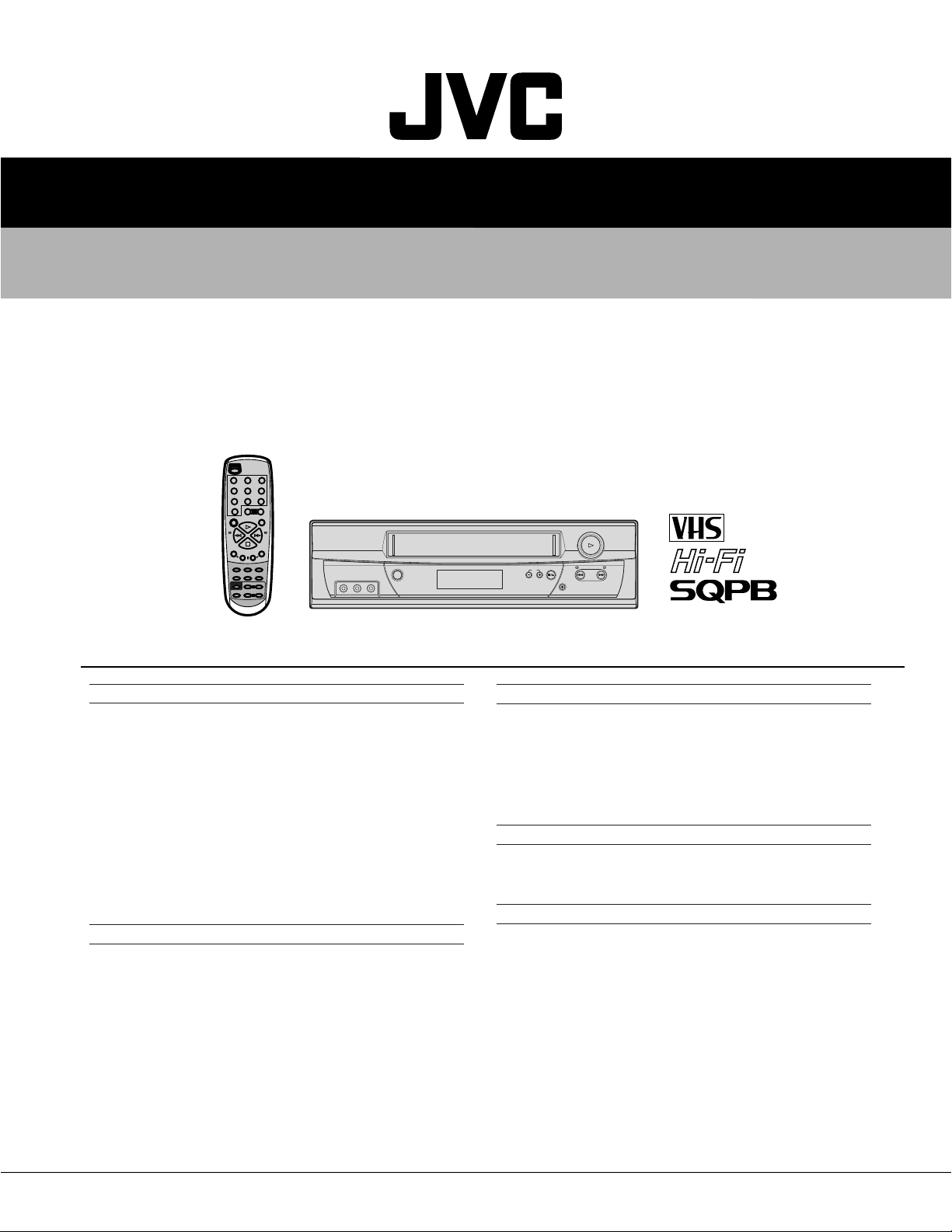
SERVICE MANUAL
VIDEO CASSETTE RECORDER
HR-A590U/A591U
POWER
12 3
456
7089
+
CH(AUX)
–
REC
PAUSE
PLAY
REW FF
MENU
STOP
+
–
SET
TV/VCR TIMER
A.MONITOR SP/EP DISPLAY
–
TV CH
TV POWER
–
TV VOL
INPUT
ENTER
CANCEL
C.RESET
+
+
VIDEO (MONO) L – AUDIO – R
POWER
CH
STOP/EJECT
PLAY
REW
FF
REC
SPECIFICATIONS
GENERAL
Power requirement
Power consumption
Power on
Power off
Temperature
Operating
Storage
Operating position
Dimensions (W x H x D)
Weight
Format
Maximum recording time
SP
EP
VIDEO/AUDIO
Signal system
Recording/Playback
system
Signal-to-noise ratio
Horizontal resolution
Frequency range
Normal audio
Hi-Fi audio
Input/Output
: AC 120 V, 60 Hz
:9 W
: 1.7 W
: °C to 40°C (41°F to 104°F)
5
:–20°C to 60°C
: Horizontal only
: 360 mm x 95 mm x 224 mm
(14-3/16" x 3-3/4" x 8-13/16")
: 3.2 kg (7.1 lbs)
: VHS NTS C standard
: 210 min. with ST -210 video cassette
: 630 min. with ST-210 video cassette
: NTS C-type color signal and
EIA monochrome signal, 525 lines/60 fields
: DA-4
(Double Azimuth) head helical scan system
: 42 dB
: 230 lines
: 100 Hz to 10,000 Hz
: 20 Hz to 20,000 Hz
:
RC A connectors (IN x 1, OUT x 1)
(The specifications shown pertain specifically to the model HR-A591U.)
TUNER
Tuning system
Channel coverage
VHF
UHF
CATV
R F output
(–4°F to140°F)
TIMER
Clock reference
Program capacity
Memory backup for timer
ACCESSORIES
Provided accessories
Specifications shown are for S P mode unless specified otherwise.
E. & O.E. Design and specifications subject to change without notice.
: Frequency-synthesized tuner
: Channels 2– 13
: Channels 14 –69
: 113 Channels
: Channel 3 or 4 (switchable; preset to
Channel 3 when shipped) 75 ohms,
unbalanced
: Quartz
: 1-month programmable timer/8 programs
: Approx. 5 sec.
: R F cable (F-type),
Infrared remote control unit,
“AAA” battery x 2
This service manual is printed on 100% recycled paper.
COPYRIGHT © 2002 VICTOR COMPANY OF JAPAN, LTD
No.82885
January 2002
Page 2

Page 3

TABLE OF CONTENTS
Section Title Page Section Title Page
Important Safety Precautions
INSTRUCTIONS
DISASSEMBLY INSTRUCTIONS
1.REMOVAL OF MECHANICAL PARTS AND
P.C.BOARDS ..................................................................1-1
1-1 TOP CABINET AND FRONT CABINET ..................1-1
1-2 FLAP .......................................................................1-1
1-3 DECK CHASSIS ..................................................... 1-1
1-4 SYSCON PCB.........................................................1-1
2.REMOVAL OF DECK PAR TS .........................................1-2
2-1 TOP BRACKET .......................................................1-2
2-2 CASSETTE HOLDER ASS’Y ..................................1-2
2-3 CASSETTE SIDE L/R .............................................1-2
2-4 LINK UNIT ...............................................................1-2
2-5 LINK LEVER/FLAP LEVER.....................................1-2
2-6 LOADING MOTOR/WORM .....................................1-3
2-7 TENSION ASS’Y .....................................................1-3
2-8 T BRAKE ARM/T BRAKE BAND .............................1-4
S REEL/T REEL/IDLER ARM ASS’Y/IDLER GEAR ........
2-9
2-10 CASSETTE OPENER/PINCH ROLLER
BLOCK/P5 ARM ASS’Y...........................................1-5
2-11 A/C HEAD ...............................................................1-5
2-12 FE HEAD(RECORDER ONLY) ...............................1-5
2-13 AHC ASS’Y/CYLINDER UNIT ASS’Y......................1-5
2-14 CAPSTAN DD UNIT ................................................1-6
2-15
MAIN CAM/PINCH ROLLER CAM/JOINT GEAR ............
LOADING GEAR S/T UNIT..............................................
2-16
CLUTCH ASS’Y/RING SPRING/
2-17
CLUTCH LEVER/CLUTCH GEAR ...................................
2-18
CASSETTE GUIDE POST/
INCLINED BASE S/T UNIT/P4 CAP ................................
REMOVAL AND INSTALLATION OF FLAT PACKAGE IC........
3.
REMOVAL........................................................................1-8
INSTALLATION ................................................................1-9
KEY TO ABBREVIATIONS .............................................1-10
PREVENTIVE CHECKS AND SERVICE INTERVALS ....1-12
CLEANING......................................................................1-12
SERVICE MODE LIST.....................................................1-13
SERVICING FIXTURES AND TOOLS............................. 1-13
MECHANISM ADJUSTMENT PARTS LOCATION GUIDE.......
MECHANICAL ADJUSTMENTS
TAPE REMOVAL METHOD AT NO POWER SUPPLY ....1-14
1.CONFIRMATION AND ADJUSTMENT ......................... 1-14
1-1 CONFIRMATION AND ADJUSTMENT OF
TENSION POST POSITION .................................1-14
1-2 CONFIRMATION OF PLAYBACK TORQUE AND
BACK TENSION TORQUE DURING PLAY BACK.. 1-14
1-3 CONFIRMATION OF VSR TORQUE .................... 1-14
1-4 CONFIRMATION OF REEL BRAKE TORQUE .....1-15
2.CONFIRMATION AND ADJUSTMENT OF
TAPE RUNNING MECHANISM ....................................1-15
2-1 GUIDE ROLLER ................................................... 1-15
2-2 CONFIRMATION AND ADJUSTMENT OF
AUDIO/CONTROL HEAD ..................................... 1-16
2-3
TAPE RUNNING ADJUSTMENT(X-VALUE ADJUSTMENT) ...
ELECTRICAL ADJUSTMENTS
1.BASIC ADJUSTMENT ..................................................1-17
1-1 SWITCHING POINT..............................................1-17
ELECTRICAL ADJUSTMENT PARTS LOCATION GUIDE ........
IC DESCRIPTIONS ......................................................... 1-18
SERVO TIMING CHART .................................................1-21
MECHANISM TIMING CHART........................................ 1-22
1-4
1-6
1-6
1-7
1-7
1-8
1-13
1-16
1-17
TROUBLESHOOTING GUIDE
POWER DOES NOT TURN ON ..............................................
POWER SHUTS OFF .................................................... 1-24
CYLINDER NOT ROTATING DURING PLAYBACK AND RECODRDING..
CASSETTE IN AND DOWN, UNIT HAS NO FUNCTIONS .....
FF/REW DO NOT WORK .............................................. 1-26
AUDIO SHAKES ............................................................ 1-26
CASSETTE TAPE IS NOT ACCEPTED.........................1-27
WHEN INSERTING CASSETTE, IT EJECTS IMMEDIATELY ..
T APE LOADING IS OK, BUT UNLOADS IMMEDIATELY..
CAPSTAN DD MOTOR NOT ROTATING ...................... 1-30
PLAYBACK PICTURE JITTERS HORIZONTALLY........1-31
PLAYBACK PICTURE SHAKES....................................1-31
AUTO TRACKING DOES NOT OPERATE ....................1-32
WHEN PLAYBACK, FAST FORWARD OR REWIND MODE IS ACTIVATED,
UNIT STOPS IMMEDIATELY
PLAYBACK PICTURE JITTERS VERTICALLY ............. 1-33
NO PLAYBACK PICTURE .............................................1-34
NO PICTURE DURING PLAYBACK..............................1-35
NO COLOR DURING SELF RECORDING AND PLAYBACK .
PLAYBACK PICTURE NOISY(EVEN AFTER CLEANING HEADS) ...
NO NORMAL AUDIO ON PLAYBACK ...........................1-37
AUDIO CAN NOT BE RECORDED ............................... 1-38
RECORDING MECHANISM WORKS,
BUT NO VIDEO RECORDED FROM INPUT JACK OR TUNER ..
NO E-E(NO VIDEO FROM TUNER)..............................1-40
NO E-E AUDIO(MONO).................................................1-41
NO TUNER AUDIO(MONO)........................................... 1-42
CHARTS AND DIAGRAMS
INTERCONNECTION DIAGRAM ......................................2-1
Y/C/AUDIO/CCD/HEAD AMP SCHEMATIC DIAGRAM .....2-3
SYSTEM CONTROL/SERVO SCHEMATIC DIAGRAM ....2-5
POWER SCHEMATIC DIAGRAM......................................2-7
HI-FI/DEMODULATOR SCHEMATIC DIAGRAM...............2-9
OPERATION SCHEMATIC DIAGRAM [HR-A591U/A591U(C)] .
OPERATION SCHEMATIC DIAGRAM [HR-A590U(C)] ...2-13
TUNER SCHEMATIC DIAGRAM [HR-A591U/A591U(C)]....
TUNER SCHEMATIC DIAGRAM [HR-A590UC]..............2-17
SYSCON CIRCUIT BOARD(INSERTED PARTS) ...........2-19
SYSCON CIRCUIT BOARD(CHIP MOUNTED PARTS).. 2-21
WAVEFORMS ..................................................................2-24
Y/C/AUDIO/HEAD AMP BLOCK DIAGRAM ....................2-25
SYSTEM CONTROL/SERVO BLOCK DIAGRAM ........... 2-27
TUNER BLOCK DIAGRAM [HR-A591U/A591U(C)] ........2-29
TUNER BLOCK DIAGRAM [HR-A590U(C)] ....................2-31
OPERATION BLOCK DIAGRAM .....................................2-33
POWER BLOCK DIAGRAM ............................................ 2-33
HI-FI/DEMODULATOR BLOCK DIAGRAM .....................2-35
PARTS LIST
3.1 P ACKING AND ACCESSOR Y ASSEMBL Y <M1> .....3-1
3.2 FINAL ASSEMBLY <M2> [HR-A591U/A591U(C)] ..... 3-2
3.3 FINAL ASSEMBLY <M2> [HR-A590U(C)] ................. 3-3
3.4 MECHANISM ASSEMBL Y <M4>............................... 3-4
3.5 ELECTRICAL PARTS LIST ....................................... 3-7
SYSCON BOARD ASSEMBLY <03>.........................3-7
Reference..........................................................................4-1
GENERAL SPECIFICATIONS [HR-A591U/A591U(C)] ......4-1
GENERAL SPECIFICATIONS [HR-A590U(C)] ..................4-6
.....................................................1-32
1-23
1-25
1-25
1-28
1-29
1-35
1-36
1-39
2-11
2-15
The following table lists the differing points between Models (HR-A591U, HR-A591U(C) and HR-A590U(C) in this series.
ITEM
INSTRUCTION LANGUAGE ENGLISH ENGLISH, FRENCH ENGLISH, FRENCH
REGISTRATION CARD USED NOT USED NOT USED
GUARANTEE CARD NOT USED USED USED
SERVICE STAION LIST NOT USED USED USED
FRONT INDICATOR FDP FDP LED
RF OUTPUT SWITCH NOT USED NOT USED USED
MODEL
HR-A591U HR-A591U(C) HR-A590U(C)
Page 4

Important Safety Precautions
cut close to connector
Prior to shipment from the factory, JVC products are strictly inspected to conform with the recognized product safety and electrical codes
of the countries in which they are to be sold. However, in order to maintain such compliance, it is equally important to implement the
following precautions when a set is being serviced.
v
Precautions during Servicing
1. Locations requiring special caution are denoted by labels and
inscriptions on the cabinet, chassis and certain parts of the
product. When performing service, be sure to read and comply with these and other cautionary notices appearing in the
operation and service manuals.
2. Parts identified by the
critical for safety.
Replace only with specified part numbers.
Note: Parts in this category also include those specified to com-
ply with X-ray emission standards for products using
cathode ray tubes and those specified for compliance
with various regulations regarding spurious radiation
emission.
3. Fuse replacement caution notice.
Caution for continued protection against fire hazard.
Replace only with same type and rated fuse(s) as specified.
4. Use specified internal wiring. Note especially:
1) Wires covered with PVC tubing
2) Double insulated wires
3) High voltage leads
5. Use specified insulating materials for hazardous live parts.
Note especially:
1) Insulation Tape 3) Spacers 5) Barrier
2) PVC tubing 4) Insulation sheets for transistors
6. When replacing AC primary side components (transformers,
power cords, noise blocking capacitors, etc.) wrap ends of
wires securely about the terminals before soldering.
symbol and shaded ( ) parts are
12. Crimp type wire connector
In such cases as when replacing the power transformer in sets
where the connections between the power cord and power
transformer primary lead wires are performed using crimp type
connectors, if replacing the connectors is unavoidable, in order to prevent safety hazards, perform carefully and precisely
according to the following steps.
1) Connector part number : E03830-001
2) Required tool : Connector crimping tool of the proper type
which will not damage insulated parts.
3) Replacement procedure
(1) Remove the old connector by cutting the wires at a point
close to the connector.
Important : Do not reuse a connector (discard it).
Fig.3
(2) Strip about 15 mm of the insulation from the ends of
the wires. If the wires are stranded, twist the strands to
avoid frayed conductors.
15 mm
Fig.1
7. Observe that wires do not contact heat producing parts
(heatsinks, oxide metal film resistors, fusible resistors, etc.)
8. Check that replaced wires do not contact sharp edged or
pointed parts.
9. When a power cord has been replaced, check that 10-15 kg of
force in any direction will not loosen it.
Power cord
Fig.2
10. Also check areas surrounding repaired locations.
11. Products using cathode ray tubes (CRTs)
In regard to such products, the cathode ray tubes themselves,
the high voltage circuits, and related circuits are specified for
compliance with recognized codes pertaining to X-ray emission.
Consequently, when servicing these products, replace the cathode ray tubes and other parts with only the specified parts.
Under no circumstances attempt to modify these circuits.
Unauthorized modification can increase the high voltage value
and cause X-ray emission from the cathode ray tube.
Fig.4
(3) Align the lengths of the wires to be connected. Insert
the wires fully into the connector.
Metal sleeve
Connector
Fig.5
(4) As shown in Fig.6, use the crimping tool to crimp the
metal sleeve at the center position. Be sure to crimp fully
to the complete closure of the tool.
1.25
2.0
5.5
Fig.6
(5) Check the four points noted in Fig.7.
Not easily pulled free
Wire insulation recessed
more than 4 mm
Fig.7
Crimping tool
Crimped at approx. center
of metal sleeve
Conductors extended
1
S40888-01
Page 5
v
d'
d
Chassis
Power cord,
primary wire
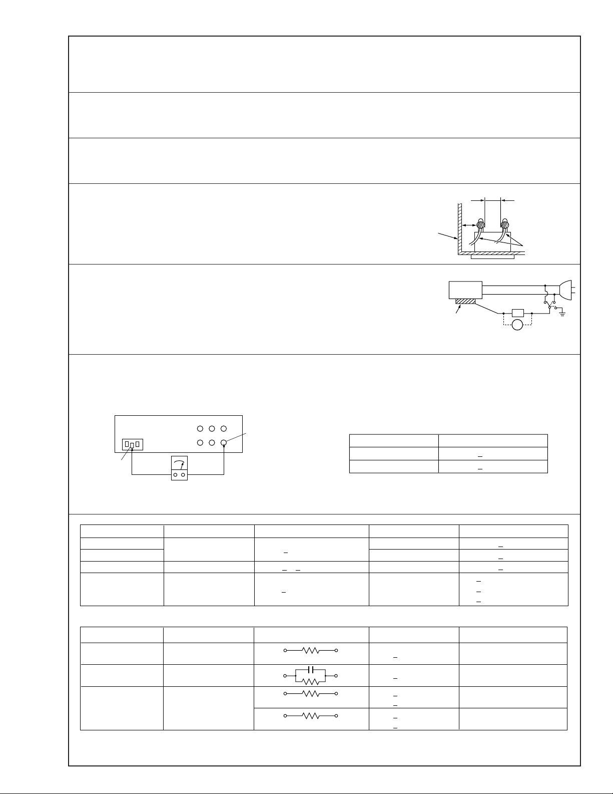
Safety Check after Servicing
Examine the area surrounding the repaired location for damage or deterioration. Observe that screws, parts and wires have been
returned to original positions, Afterwards, perform the following tests and confirm the specified values in order to verify compliance with safety standards.
1. Insulation resistance test
Confirm the specified insulation resistance or greater between power cord plug prongs and
externally exposed parts of the set (RF terminals, antenna terminals, video and audio input
and output terminals, microphone jacks, earphone jacks, etc.). See table 1 below.
2. Dielectric strength test
Confirm specified dielectric strength or greater between power cord plug prongs and exposed
accessible parts of the set (RF terminals, antenna terminals, video and audio input and output
terminals, microphone jacks, earphone jacks, etc.). See table 1 below.
3. Clearance distance
When replacing primary circuit components, confirm specified clearance distance (d), (d’) between soldered terminals, and between terminals and surrounding metallic parts. See table 1
below.
Fig. 8
4. Leakage current test
Confirm specified or lower leakage current between earth ground/power cord plug prongs
and externally exposed accessible parts (RF terminals, antenna terminals, video and audio
input and output terminals, microphone jacks, earphone jacks, etc.).
Measuring Method : (Power ON)
Insert load Z between earth ground/power cord plug prongs and externally exposed accessible parts. Use an AC voltmeter to measure across both terminals of load Z. See figure 9 and
following table 2.
Externally
exposed
accessible part
Z
V
Fig. 9
ab
c
5. Grounding (Class 1 model only)
Confirm specified or lower grounding impedance between earth pin in AC inlet and externally exposed accessible parts (Video in,
Video out, Audio in, Audio out or Fixing screw etc.).
Measuring Method:
Connect milli ohm meter between earth pin in AC inlet and exposed accessible parts. See figure 10 and grounding specifications.
AC inlet
Earth pin
AC Line Voltage
100 V
100 to 240 V
110 to 130 V
110 to 130 V
200 to 240 V
Exposed accessible part
Milli ohm meter
Fig. 10
Region
Japan
USA & Canada
Europe & Australia R 10 MΩ/500 V DC
Region Load Z
Insulation Resistance (R)
≤
R 1 MΩ/500 V DC
≥≥
1 MΩ R 12 MΩ/500 V DC
≤
Table 1 Specifications for each region
Grounding Specifications
Region
USA & Canada
Europe & Australia
Dielectric Strength
AC 1 kV 1 minute
AC 1.5 kV 1 miute
AC 1 kV 1 minute
AC 3 kV 1 minute
AC 1.5 kV 1 minute
(Class 2)
(Class 1)
Grounding Impedance (Z)
≤
Z 0.1 ohm
≤
Z 0.5 ohm
Clearance Distance (d), (d')
≤
d, d' 3 mm
≤
d, d' 4 mm
≤
d, d' 3.2 mm
≤
d 4 mm
≤
d' 8 mm (Power cord)
≤
d' 6 mm (Primary wire)
a, b, cLeakage Current (i)AC Line Voltage
100 V
110 to 130 V
110 to 130 V
220 to 240 V
Note: These tables are unofficial and for reference only. Be sure to confirm the precise values for your particular country and locality.
Japan
USA & Canada
Europe & Australia
Table 2 Leakage current specifications for each region
1 kΩ
0.15 µF
1.5 kΩ
2 kΩ
50 kΩ
2
≤
i 1 mA rms Exposed accessible parts
≤
i 0.5 mA rms
≤
i 0.7 mA peak
≤
i 2 mA dc
≤
i 0.7 mA peak
≤
i 2 mA dc
Exposed accessible parts
Antenna earth terminals
Other terminals
S40888-01
Page 6

Page 7
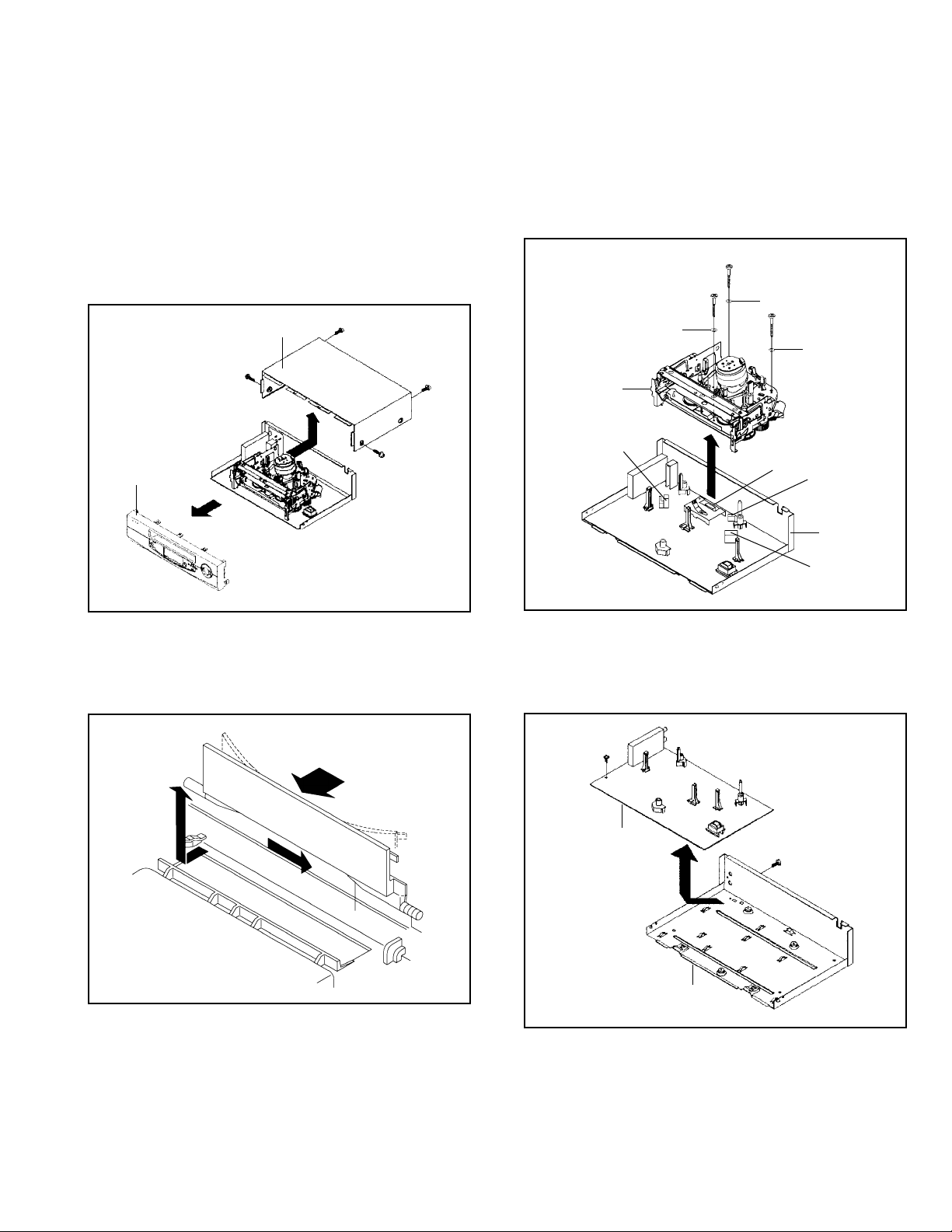
DISASSEMBLY INSTRUCTIONS
1.
REMOVAL OF MECHANICAL PARTS
AND P.C. BOARDS
1-1:
TOP CABINET AND FRONT CABINET
(Refer to Fig. 2-1)
1.
Remove the 4 screws 1.
2.
Remove the Top Cabinet in the direction of arrow (A).
3.
Unlock the 7 supports 2.
4.
Remove the Front Cabinet in the direction of arrow (B).
1
1
Front Cabinet
2
2
Top Cabinet
1
(A)
(B)
2
2
2
2
2
1
Fig. 1-1
1-3: DECK CHASSIS (Refer to Fig. 1-3)
1.
Remove the 3 screws 1.
2.
Disconnect the following connectors: (CP1001, CP4001,
CP4002 and CP4003).
3.
Remove the Deck Chassis in the direction of arrow.
1
1
Washer
Deck Chassis
CP4003
Washer
1
CP4001
Washer
CP4002
Bottom Plate
CP1001
Fig. 1-3
1-2: FLAP (Refer to Fig. 1-2)
1.2.Open Flap to 90˚ and flex in direction of arrow (A), at the
same time slide in direction of arrow (B).
Then lift in direction of arrow (C).
(A)
(C)
(B)
Flap
Fig. 1-2
1-4: SYSCON PCB (Refer to Fig. 1-4)
1.
Remove the screw 1.
2.
Remove the screw 2.
3.
Remove the Syscon PCB in the direction of arrow.
2
Syscon PCB
Bottom Plate
1
Fig. 1-4
1-1
Page 8

DISASSEMBLY INSTRUCTIONS
2. REMOVAL OF DECK PARTS
2-1: TOP BRACKET (Refer to Fig. 2-1)
Extend the 2 supports 1.
1.
Slide the 2 supports 2 and remove the Top Bracket.
2.
NOTE
After the installation of the Top Bracket, bend the support
1.
1 so that the Top Bracket is fixed.
Top Bracket
1
Top Bracket
2
Main Chassis
2
Main Chassis
2-2: CASSETTE HOLDER ASS'Y (Refer to Fig. 2-2)
1.
Move the Cassette Holder Ass'y to the front side.
2.
Push the Locker R to remove the Cassette Side R.
3.
Remove the Cassette Side L.
Cassette Side R
Main Chassis
1
Locker R
Fig. 2-1
NOTE
In case of the Locker R installation, check if the two
1.
positions of Fig. 2-3-B are correctly locked.
When you install the Cassette Side R, be sure to move
2.
the Locker R after installing.
Locker R
Check if these
Cassette Side R
positions are locked.
2-4: LINK UNIT (Refer to Fig. 2-4)
1.
Set the Link Unit to the Eject position.
2.
Unlock the support 1.
3.
Remove the (A) side of the Link Unit first, then remove
the (B) side.
Main Chassis
Link Unit
Fig. 2-3-B
Link Unit
Cassette Side L
Main Chassis
2-3: CASSETTE SIDE L/R (Refer to Fig. 2-3-A)
1.
Remove the Locker Spring.
2.
Unlock the 4 supports 1 and then remove the Cassette
Side L/R.
3.
Unlock the support 2 and then remove the Locker R.
Locker Spring
1
1
2
Cassette Side R
Cassette Holder
Locker R
1
1
Cassette Side L
Fig. 2-2
(A)
(B)
Link Unit
Main Chassis
2-5: LINK LEVER/FLAP LEVER (Refer to Fig. 2-5)
1.
Extend the support 1.
2.
Remove the Link Lever.
3.
Remove the Flap Lever.
1
Flap Lever
Link Lever
Fig. 2-4
Fig. 2-5
1-2
Fig. 2-3-A
Page 9
DISASSEMBLY INSTRUCTIONS
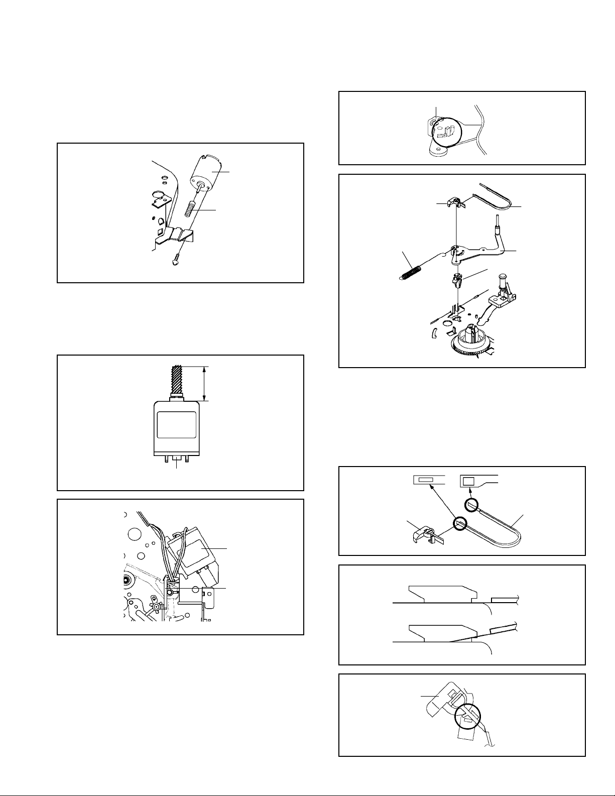
2-6: LOADING MOTOR/WORM (Refer to Fig. 2-6-A)
1.
Remove the screw 1.
2.
Remove the Loading Motor.
3.
Remove the Worm.
Loading Motor
Worm
Main Chassis
• Screw Torque: 3 ± 0.5kgf•cm
1
Fig. 2-6-A
NOTE
1.2.In case of the Worm installation, check if the value of the
Fig. 2-6-B is correct.
In case of the Loading Motor installation, hook the wire
on the Cassette Opener as shown Fig. 2-6-C.
19.2 ± 0.1mm
Safety surface for pressing
of the insert.
Fig. 2-6-B
Tension Arm Ass’y
Fig. 2-7-A
1
Tension Connect
Tension Spring
2
4
1
3
Tension Holder
Tension Band
Tension Arm Ass’y
Fig. 2-7-B
NOTE
1.
In case of the Tension Band installation, note the direction of the installation. (Refer to Fig. 2-7-C)
2.
In case of the Tension Band installation, install correctly
as Fig. 2-7-D.
3.
In case of the Tension Connect installation, install as the
circled section of Fig. 2-7-E.
Loading Motor
Cassette Opener
Fig. 2-6-C
2-7: TENSION ASS’Y (Refer to Fig. 2-7-B)
1.
Turn the Pinch Roller Cam clockwise so that the Tension
Holder hook is set to the position of Fig. 2-7-A to move
the Tension Arm Ass’y.
2.
Remove the Tension Spring.
3.
Unlock the 2 supports 1 and remove the Tension Band.
4.
Unlock the support 2 and remove the Tension Arm Ass’y.
5.
Unlock the support 3 and remove the Tension Connect.
6.
Float the hook 4 and turn it clockwise then remove the
Tension Holder.
Tension Connect
[OK]
[NG]
Tension Connect
Tension Connect
Tension Connect
Main Chassis
Tension Band
Fig. 2-7-C
Tension Band
Tension Band
Fig. 2-7-D
Fig. 2-7-E
1-3
Page 10
DISASSEMBLY INSTRUCTIONS
2-8: T BRAKE ARM/T BRAKE BAND (Refer to Fig. 2-8-A)
Remove the T Brake Spring.
1.
Turn the T Brake Arm clockwise and bend the hook
2.
section to remove it.
Unlock the 2 supports 1 and remove the T Brake Band.
3.
T Brake Band
Hook section
1
1
T Brake Arm
T Brake Spring
Idler Gear
(A)
Idler Arm Ass’y
(B)
S Reel
T Reel
1
(A)
1
Fig. 2-8-A
NOTE
1. In case of the T Brake Band installation, install correctly
as Fig. 2-8-B.
[OK]
T Brake Band
[NG]
T Brake Band
T Brake Arm
T Brake Arm
Fig. 2-8-B
2-9: S REEL/T REEL/IDLER ARM ASS’Y/IDLER GEAR
(Refer to Fig. 2-9-A)
1.
Remove the S Reel and T Reel.
2.
Remove the 2 Polyslider Washers 1.
3.
Remove the Idler Arm Ass’y and Idler Gear.
NOTE
1.
Take care not to damage the gears of the S Reel and T
Reel.
2.
The Polyslider Washer may be remained on the back of
the reel.
3.
Take care not to damage the shaft.
4.
Do not touch the section “A” of S Reel and T Reel. (Use
gloves.) (Refer to Fig. 2-9-A) Do not adhere the stains
on it.
5.
When you install the reel, clean the shaft and grease it
(FG-84M). (If you do not grease, noise may be heard in
FF/REW mode.)
6.
After installing the reel, adjust the height of the reel.
(Refer to MECHANICAL ADJUSTMENT)
Fig. 2-9-A
NOTE
1.2.In case of the S Reel and T Reel installation, check if the
correct parts are installed. (Refer to Fig. 2-9-B)
In case of the Idler Arm Ass’y installation, install correctly
as Fig. 2-9-C. And also set it so that the section “B” of
Fig. 2-9-A is placed under the Main Chassis tab.
Big Hole
(S Reel)
Small Hole
(T Reel)
Fig. 2-9-B
[OK]
Clutch Gear
Idler Arm Ass’y
[NG]
Idler Arm Ass’y
Clutch Gear
Fig. 2-9-C
1-4
Page 11
DISASSEMBLY INSTRUCTIONS
2-10: CASSETTE OPENER/PINCH ROLLER BLOCK/P5
ARM ASS’Y (Refer to Fig. 2-10-A)
1.2.Unlock the support 1 and remove the Cassette Opener.
Remove the Pinch Roller Block and P5 Arm Ass’y.
1
Cassette Opener
Pinch Roller Block
P5 Arm Ass’y
Main Chassis
Fig. 2-10-A
NOTE
1.2.Do not touch the Pinch Roller. (Use gloves.)
In case of the Pinch Roller Block and the Pinch Roller
Cam installation, install correctly as Fig. 2-10-B.
Pinch Roller Block
P5 Arm Ass’y
Can be seen the hole of the
Main Cam.
Can be seen the hole of
the Pinch Roller Cam.
Fig. 2-10-B
2-11: A/C HEAD (Refer to Fig. 2-11-A)
1.
Remove the screw 1.
2.
Remove the A/C Head Base.
3.
Remove the 3 screws 2.
4.
Remove the A/C Head and A/C Head Spring.
NOTE
1.
Do not touch the A/C Head. (Use gloves.)
2.
When you install the A/C Head Spring, install as shown in
Fig. 2-11-B.
3.
When you install the A/C Head, tighten the screw (1) first,
then tighten the screw (2), finally tighten the screw (3).
(3)
(1)
2
2
(2)
2
A/C Head
Spring Position
Fig. 2-11-B
2-12: FE HEAD (RECORDER ONLY) (Refer to Fig. 2-12)
1.2.Remove the screw 1.
Remove the FE Head.
1
FE Head
• Screw Torque: 5 ± 0.5kgf•cm
• The FE Head is not installed on the Video Cassette Player.
Fig. 2-12
2-13: AHC ASS’Y/CYLINDER UNIT ASS’Y
(Refer to Fig. 2-13)
1.
Disconnect the following connector:
(CD2001)
2.
Remove the 3 screws 1.
3.
Remove the Cylinder Unit Ass’y.
NOTE
1. When you install the Cylinder Unit Ass’y, tighten the
screws from (1) to (3) in order while pulling the Ass’y
toward the left front direction.
CD2001
Cylinder Unit Ass’y
1
• Screw Torque: 5 ± 0.5kgf•cm (Screw 1)
A/C Head Spring
A/C Head Base
Fig. 2-11-A
• Screw Torque: 3 ± 0.5kgf•cm
(3)
(2)
(1)
1
1
1
Fig. 2-13
1-5
Page 12
DISASSEMBLY INSTRUCTIONS
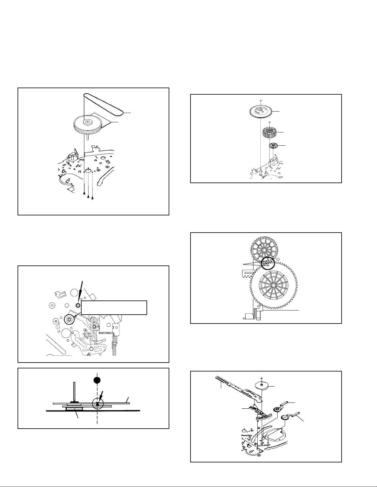
2-14: CAPSTAN DD UNIT (Refer to Fig. 2-14-A)
1.
Remove the Capstan Belt.
2.
Remove the 3 screws 1.
3.
Remove the Capstan DD Unit.
Capstan Belt
Capstan DD Unit
1
1
1
• Screw Torque: 4 ± 0.5kgf•cm
Fig. 2-14-A
NOTE
1. In case of the Capstan DD Unit installation, apply the
silicon bond (TSE3843-W) on the position Fig. 2-14-B
correctly. (If no silicon bond applied, abnormal noise will
be heard on the deck operation.)
(Refer to Fig. 2-14-B, C)
Applied position of
silicon bond
2-15: MAIN CAM/PINCH ROLLER CAM/JOINT GEAR
(Refer to Fig. 2-15-A)
1.2.Remove the E-Ring 1, then remove the Main Cam.
Remove the E-Ring 2, then remove the Pinch Roller
Cam and Joint Gear.
1
Main Cam
2
Pinch Roller Cam
Joint Gear
Fig. 2-15-A
NOTE
1. In case of the Pinch Roller Cam and Main Cam installation, install them as the circled section of Fig. 2-15-B so
that the each markers are met. (Refer to Fig. 2-15-B)
And also can be seen the Main Chassis hole through the
Main Cam maker hole.
Pinch Roller Cam
Marker
Main Cam
1-6
Be careful not to apply the silicon
bond to the Pinch Roller.
Capstan DD Unit
Silicon Bond
Main Chassis
Fig. 2-14-B
Fig. 2-14-C
Fig. 2-15-B
2-16: LOADING GEAR S/T UNIT (Refer to Fig. 2-16-A)
1.2.Remove the E-Ring 1 and remove the Main Loading
Gear.
Remove the Main Rod, Tension Lever, Loading Arm S
Unit and Loading Arm T Unit.
1
Main Rod
Tension Lever
Main Loading Gear
Loading Arm T Unit
Loading Arm S Unit
Fig. 2-16-A
Page 13
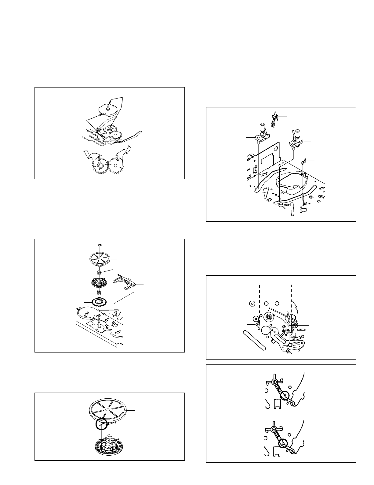
DISASSEMBLY INSTRUCTIONS
NOTE
1. When you install the Loading Arm S Unit, Loading Arm T
Unit and Main Loading Gear, align each marker. (Refer
to Fig. 2-16-B)
Marker
Main Loading Gear
Marker
Loading Arm T Unit Loading Arm S Unit
Fig. 2-16-B
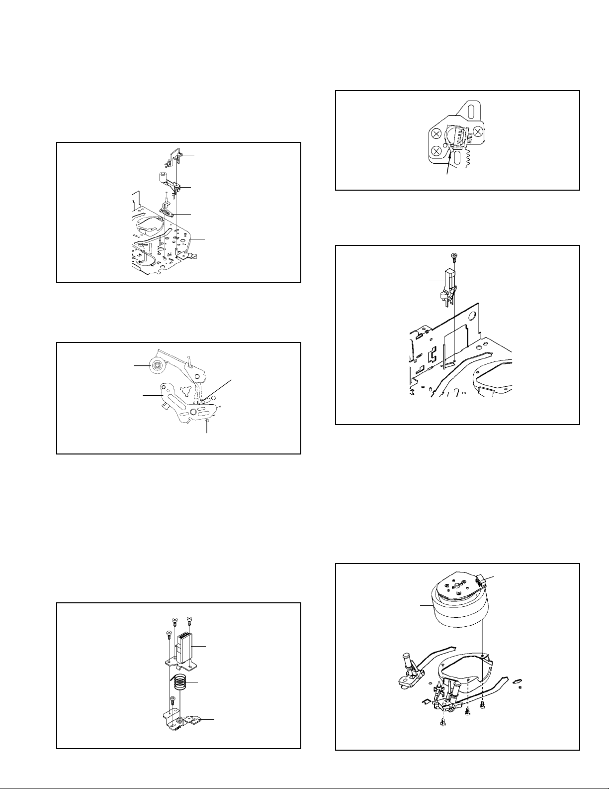
2-17: CLUTCH ASS’Y/RING SPRING/CLUTCH LEVER/
CLUTCH GEAR (Refer to Fig. 2-17-A)
1.
Remove the Polyslider Washer 1.
2.
Remove the Clutch Ass’y and Ring Spring.
3.
Remove the Clutch Lever.
4.
Remove the Coupling Gear, Coupling Spring and Clutch
Gear.
1
Clutch Ass’y
Ring Spring
2-18: CASSETTE GUIDE POST/INCLINED BASE S/T
UNIT/P4 CAP (Refer to Fig. 2-18-A)
1.
Remove the P4 Cap.
2.
Unlock the support 1 and remove the Cassette Guide
Post.
3.
Remove the Inclined Base S Unit and Inclined Base T
Unit.
1
Inclined Base S
Unit Inclined Base T
Cassette Guide Post
Unit
P4 Cap
Fig. 2-18-A
NOTE
1.
Do not touch the roller of Guide Roller.
2.
In case of the P4 Cap installation, install it with parallel
for “A” and “B” of Fig. 2-18-B.
3.
In case of the Cassette Guide Post installation, install
correctly as the circled section of Fig. 2-18-C.
Coupling Gear
Coupling Spring
Clutch Gear
Clutch Lever
Fig. 2-17-A
NOTE
1. In case of the Clutch Ass’y installation, install it with
inserting the spring of the Clutch Ass’y into the dent of the
Coupling Gear. (Refer to Fig. 2-17-B)
Clutch Ass’y
Coupling Gear
Fig. 2-17-B
“A” “B”
P4 Cap
[OK]
Cassette Guide Post
[NG]
Cassette Guide Post
Cassette Opener
Fig. 2-18-B
Fig. 2-18-C
1-7
Page 14
DISASSEMBLY INSTRUCTIONS
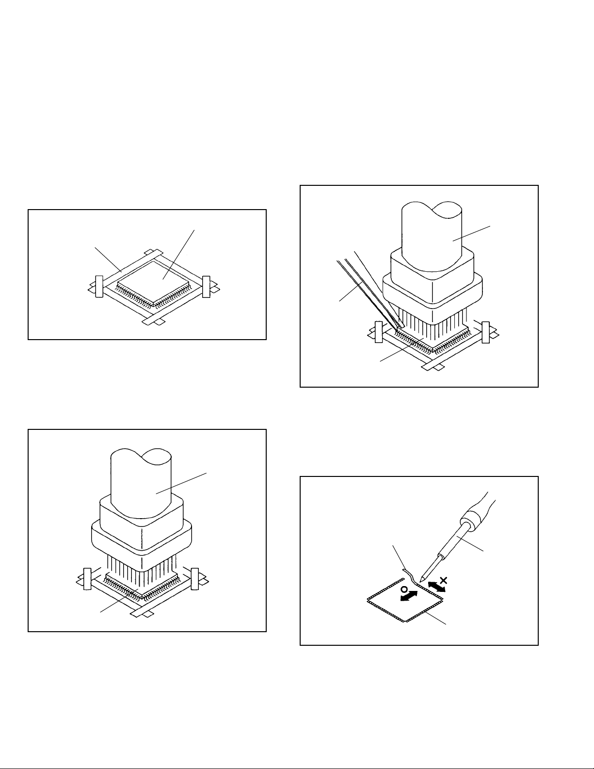
3. REMOVAL AND INSTALLATION OF FLAT PACKAGE IC
REMOVAL
1. Put the Masking Tape (cotton tape) around the Flat
Package IC to protect other parts from any damage.
(Refer to Fig. 3-1.)
NOTE
Masking is carried out on all the parts located within
10 mm distance from IC leads.
Masking T ape
(Cotton Tape)
2. Heat the IC leads using a blower type IC desoldering
machine. (Refer to Fig. 3-2.)
NOTE
Do not add the rotating and the back and forth directions force on the IC, until IC can move back and forth
easily after desoldering the IC leads completely.
IC
Fig. 3-1
Blower type IC
desoldering machine
3. When IC starts moving back and forth easily after
desoldering completely, pickup the corner of the IC using
a tweezers and remove the IC by moving with the IC
desoldering machine. (Refer to Fig. 3-3.)
NOTE
Some ICs on the PCB are affixed with glue, so be
careful not to break or damage the foil of each IC
leads or solder lands under the IC when removing it.
Blower type IC
desoldering machine
Tweezers
IC
4.5.Peel off the Masking Tape.
Absorb the solder left on the pattern using the Braided
Shield Wire. (Refer to Fig. 3-4.)
NOTE
Do not move the Braided Shield Wire in the vertical
direction towards the IC pattern.
Fig. 3-3
1-8
Braided Shield Wire
Soldering Iron
IC
Fig. 3-2
IC pattern
Fig. 3-4
Page 15

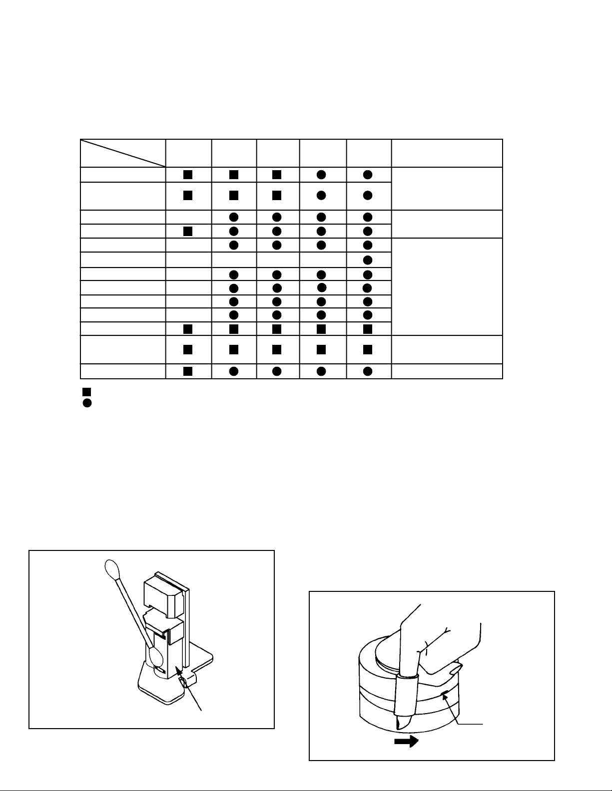
DISASSEMBLY INSTRUCTIONS
INSTALLATION
1. Take care of the polarity of new IC and then install the
new IC fitting on the printed circuit pattern. Then solder
each lead on the diagonal positions of IC temporarily.
(Refer to Fig. 3-5.)
Soldering Iron
Solder temporarily Solder temporarily
Fig. 3-5
2. Supply the solder from the upper position of IC leads
sliding to the lower position of the IC leads.
(Refer to Fig. 3-6.)
4. When bridge-soldering between terminals and/or the
soldering amount are not enough, resolder using a Thintip Soldering Iron. (Refer to Fig. 3-8.)
IC
Thin-tip Soldering Iron
Fig. 3-8
5. Finally, confirm the soldering status on four sides of the
IC using a magnifying glass.
Confirm that no abnormality is found on the soldering
position and installation position of the parts around the
IC. If some abnormality is found, correct by resoldering.
NOTE
When the IC leads are bent during soldering and/or
repairing, do not repair the bending of leads. If the
bending of leads are repaired, the pattern may be
damaged. So, be always sure to replace the IC in this
case.
Solder
IC
Supply soldering
from upper position
to lower position
Soldering Iron
3. Absorb the solder left on the lead using the Braided
Shield Wire. (Refer to Fig. 3-7.)
NOTE
Do not absorb the solder to excess.
Soldering Iron
IC
Braided Shield Wire
Fig. 3-6
Fig. 3-7
1-9
Page 16

A
A/C
ACC
AE
AFC
AFT
AFT DET
AGC
AMP
ANT
A.PB
APC
ASS’Y
AT
AUTO
A/V
B
BGP
BOT
BPF
BRAKE SOL
BUFF
B/W
C
C
CASE
CAP
CARR
CH
CLK
CLOCK (SY-SE)
COMB
CONV
CPM
CTL
CYL
CYL-M
CYL SENS
D
DATA (SY-CE)
dB
DC
DD Unit
DEMOD
DET
DEV
E
E
EF
EMPH
ENC
ENV
EOT
EQ
EXT
F
F
FBC
FE
FF
FG
FL SW
FM
FSC
FWD
G
GEN
GND
H
H.P.F
KEY TO ABBREVIATIONS
:
Audio/Control
:
Automatic Color Control
:
Audio Erase
:
Automatic Frequency Control
:
Automatic Fine Tuning
:
Automatic Fine Tuning Detect
:
Automatic Gain Control
:
Amplifier
:
Antenna
:
Audio Playback
:
Automatic Phase Control
:
Assembly
:
All Time
:
Automatic
:
Audio/Video
:
Burst Gate Pulse
:
Beginning of Tape
:
Bandpass Filter
:
Brake Solenoid
:
Buffer
:
Black and White
:
Capacitance, Collector
:
Cassette
:
Capstan
:
Carrier
:
Channel
:
Clock
:
Clock (Syscon to Servo)
:
Combination, Comb Filter
:
Converter
:
Capstan Motor
:
Control
:
Cylinder
:
Cylinder-Motor
:
Cylinder-Sensor
:
Data (Syscon to Servo)
:
Decibel
:
Direct Current
:
Direct Drive Motor Unit
:
Demodulator
:
Detector
:
Deviation
:
Emitter
:
Emitter Follower
:
Emphasis
:
Encoder
:
Envelope
:
End of Tape
:
Equalizer
:
External
:
Fuse
:
Feed Back Clamp
:
Full Erase
:
Fast Forward, Flipflop
:
Frequency Generator
:
Front Loading Switch
:
Frequency Modulation
:
Frequency Sub Carrier
:
Forward
:
Generator
:
Ground
:
High Pass Filter
H.SW
Hz
I
IC
IF
IND
INV
K
KIL
L
L
LED
LIMIT AMP
LM, LDM
LP
L.P.F
LUMI.
M
M
MAX
MINI
MIX
MM
MOD
MPX
MS SW
N
NC
NR
O
OSC
OPE
P
PB
PB CTL
PB-C
PB-Y
PCB
P. CON
PD
PG
P-P
R
R
REC
REC-C
REC-Y
REEL BRK
REEL S
REF
REG
REW
REV , RVS
RF
RMC
RY
S
S. CLK
S. COM
S. DATA
SEG
SEL
SENS
SER
SI
SIF
SO
SOL
SP
STB
SW
:
Head Switch
:
Hertz
:
Integrated Circuit
:
Intermediate Frequency
:
Indicator
:
Inverter
:
Killer
:
Left
:
Light Emitting Diode
:
Limiter Amplifier
:
Loading Motor
:
Long Play
:
Low Pass Filter
:
Luminance
:
Motor
:
Maximum
:
Minimum
:
Mixer, mixing
:
Monostable Multivibrator
:
Modulator, Modulation
:
Multiplexer, Multiplex
:
Mecha State Switch
:
Non Connection
:
Noise Reduction
:
Oscillator
:
Operation
:
Playback
:
Playback Control
:
Playback-Chrominance
:
Playback-Luminance
:
Printed Circuit Board
:
Power Control
:
Phase Detector
:
Pulse Generator
:
Peak-to Peak
:
Right
:
Recording
:
Recording-Chrominance
:
Recording-Luminance
:
Reel Brake
:
Reel Sensor
:
Reference
:
Regulated, Regulator
:
Rewind
:
Reverse
:
Radio Frequency
:
Remote Control
:
Relay
:
Serial Clock
:
Sensor Common
:
Serial Data
:
Segment
:
Select, Selector
:
Sensor
:
Search Mode
:
Serial Input
:
Sound Intermediate Frequency
:
Serial Output
:
Solenoid
:
Standard Play
:
Serial Strobe
:
Switch
1-10
Page 17

S
SYNC
SYNC SEP
T
TR
TRAC
TRICK PB
TP
U
UNREG
V
V
VCO
VIF
VP
V.PB
VR
V.REC
VSF
VSR
VSS
V-SYNC
VT
X
X’TAL
Y
Y/C
KEY TO ABBREVIATIONS
:
Synchronization
:
Sync Separator, Separation
:
Transistor
:
Tracking
:
Trick Playback
:
Test Point
:
Unregulated
:
Volt
:
Voltage Controlled Oscillator
:
Video Intermediate Frequency
:
Vertical Pulse, Voltage Display
:
Video Playback
:
Variable Resistor
:
Video Recording
:
Visual Search Fast Forward
:
Visual Search Rewind
:
Voltage Super Source
:
Vertical-Synchronization
:
Voltage Tuning
:
Crystal
:
Luminance/Chrominance
1-11
Page 18
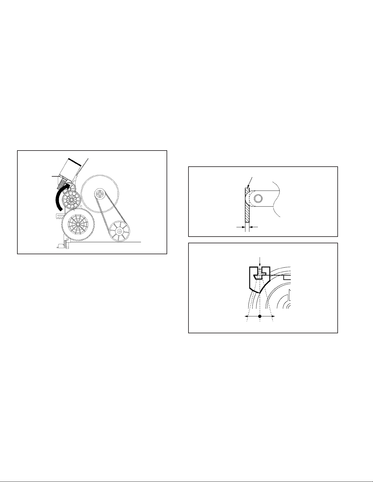
PREVENTIVE CHECKS AND SERVICE INTERVALS
The following standard table depends on environmental conditions and usage.
Parts replacing time does not mean the life span for individual parts.
Also, long term storage or misuse may cause transformation and aging of rubber parts.
The following list means standard hours, so the checking hours depends on the conditions.
Time
Parts Name
Audio Control Head
Full Erase Head
(Recorder only)
Capstan Belt
Pinch Roller
Capstan DD Unit
Loading Motor
Tension Band
T Brake Band
Clutch Ass’y
Idler Arm Ass’y
Capstan Shaft
Tape Running
Guide Post
Cylinder Unit
: Clean
: Check it and if necessary, replace it.
500
hours
1,000
hours
CLEANING
NOTE
After cleaning the heads with isopropyl alcohol, do not
run a tape until the heads dry completely. If the heads are
not completely dry and alcohol gets on the tape, damage
may occur.
1. AUDIO CONTROL HEAD
Clean the Audio Control Head with the cotton stick
soaked by alcohol. Clean the full erase head in the same
manner. (Refer to the figure below.)
1,500
hours
2,000
hours
2. TAPE RUNNING SYSTEM
When cleaning the tape transport system, use the gauze
moistened with isopropyl alcohol.
3. CYLINDER
Wrap a piece of chamois around your finger. Dip it in
isopropyl alcohol. Hold it to the cylinder head softly.
Turn the cylinder head counterclockwise to clean it (in the
direction of the arrow). (Refer to the figure below.)
NOTE
Do not exert force against the cylinder head. Do not move
the chamois upward or downward on the head.
Use the chamois one by one.
2,500
hours
Notes
Clean those parts in
contact with the tape.
Clean the rubber, and parts
which the rubber touches.
Replace when rolling
becomes abnormal.
Clean the Head
1-12
Audio Control Head
Cylinder Head
Page 19

SERVICE MODE LIST
This unit provided with the following SERVICE MODES so you can repair, examine and adjust easily.
Method Operations
Press the ATR button on the
remote control for more than
2 seconds during PLAY.
Make the short circuit
between the test point of
SERVICE and the GND.
VHS Alignment T ape
MHP
Torque Tape
PUJ48076-2
Adjusting of the Tracking to the center position.
Refer to the “MECHANICAL ADJUSTMENT” (GUIDE ROLLER) and “ELECTRICAL
ADJUSTMENT” (SWITHCHING POINT).
The BOT, EOT, and the Reel Sensor do not work and the deck can be operated
without a cassette tape.
Refer to the “PREPARATION FOR SERVICING”
SERVICING FIXTURES AND TOOLS
VHS Alignment T ape
MHP-L
Short Jumper
Torque Gauge
PUJ48075-2
Roller Driver
PTU94002-2
X-JG153 X Value Adjustment
Screwdriver
MECHANISM ADJUSTMENT PARTS LOCATION GUIDE
4
5
1. Tension Connect
2. Tension Arm
3. Guide Roller
4. Audio/Control Head
5. X value adjustment driver hole
6. P4 Post
6
3
2
1
8910
7. T Brake Spring
8. T Reel
9. S Reel
10. Adjusting section for the Tension Arm position
7
1-13
Page 20
MECHANICAL ADJUSTMENTS
TAPE REMOVAL METHOD AT NO POWER SUPPLY
1. Remove the Top Cabinet and Front Cabinet.
(Refer to item 1 of the DISASSEMBLY INSTRUCTIONS.)
2. Remove the screw 1 of the Deck Chassis and remove
the Loading Motor.
3. Rotate the Pinch Roller Cam in the direction of the arrow
by hand to slacken the Video Tape.
4. Rotate the Clutch Ass'y either of the directions to wind
the Video Tape in the Cassette Case.
5. Repeat the above step 3~4. Then take out the Video
Cassette from the Deck Chassis.
Be careful not toscratch on the tape.
Loading Motor
Screw 1
Capstan DD Unit
Pinch Roller Cam
Main Cam
Clutch Ass'y
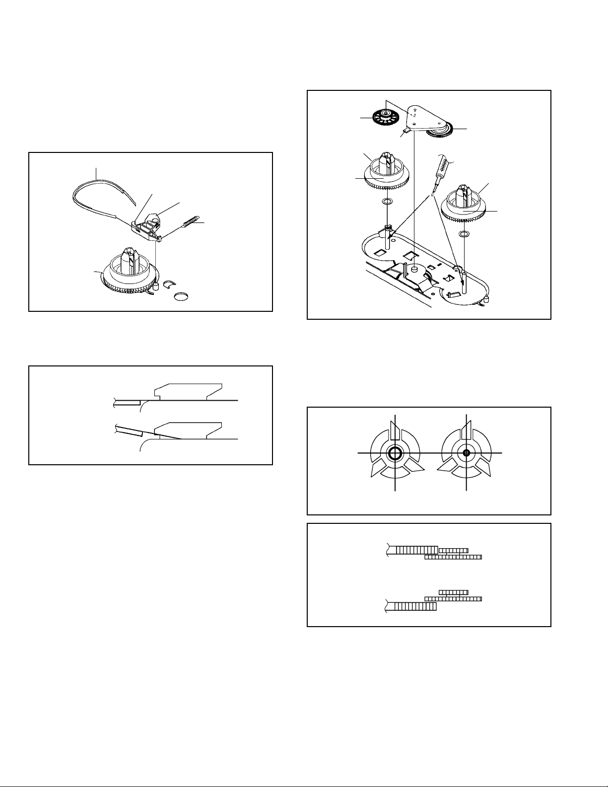
1. CONFIRMATION AND ADJUSTMENT
Read the following NOTES before starting work.
• Place an object which weighs between 450g~500g on the
Cassette Tape to keep it steady when you want to make
the tape run without the Cassette Holder. (Do not place
an object which weighs over 500g.)
1-1: CONFIRMATION AND ADJUSTMENT OF TENSION
POST POSITION
1.
Set to the PLAY mode.
2.
Adjust the adjusting section for the Tension Arm position
so that the Tension Arm top is within the standard line of
Main Chassis.
3.
While turning the S Reel clockwise, confirm that the edge
of the Tension Arm is located in the position described
above.
Standard line of Main Chassis
T ension Arm
0.5mm (Adjusting range)
Fig. 1-2-A
Main Chassis (Front Side)
Adjusting section for the
T ension Arm position
Tension Band
The Tension Arm top will
move to the inside direction
of the Main Chassis.
Bend
The Tension Arm top will
move to the outside direction
of the Main Chassis.
Fig. 1-2-B
1-2: CONFIRMATION OF PLAYBACK TORQUE AND
BACK TENSION TORQUE DURING PLAYBACK
1.
After confirmation and adjustment of Tension Post
position (Refer to item 1-2), load the cassette type
torque tape and set to the PLAY mode.
2.
Confirm that the right meter of the torque tape indicates
50~90gf•cm during playback in SP mode.
3.
Confirm that the left meter of the torque tape indicates
25~40gf•cm during playback in SP mode.
1-3: CONFIRMATION OF VSR TORQUE
1.2.Install the Torque Gauge on the S Reel. Set to the Picture
Search (Rewind) mode. (Refer to Fig.1-4-B)
Then, confirm that it indicates 120~180gf•cm.
NOTE
Install the Torque Gauge on the reel disk firmly. Press the
REW button to turn the reel disk.
1-14
Page 21
MECHANICAL ADJUSTMENTS
1-4: CONFIRMATION OF REEL BRAKE TORQUE
(S Reel Brake) (Refer to Fig. 1-4-B)
1.
Once set to the Fast Forward mode then set to the Stop
mode. While, unplug the AC cord when the Pinch Roller
Block is on the position of Fig. 1-4-A.
2.
Move the Idler Ass’y from the S Reel.
3.
Install the Torque Gauge on the S Reel. Turn the Torque
Gauge clockwise.
4.
Then, confirm that it indicates 60~100gf•cm.
(T Reel Brake) (Refer to Fig. 1-4-B)
1.
Once set to the Fast Forward mode then set to the Stop
mode. While, unplug the AC cord when the Pinch Roller
Block is on the position of Fig. 1-4-A.
2.
Move the Idler Ass’y from the T Reel.
3.
Install the Torque Gauge on the T reel. Turn the Torque
Gauge counterclockwise.
4.
Then, confirm that it indicates 30~50gf•cm.
The position at FF mode.
Pinch Roller Block
Stop at this position.
The position at
STOP mode.
Capstan DD Unit
Cassette Holder Ass’y
Cassette Opener
Fig. 1-4-A
2. CONFIRMA TION AND ADJUSTMENT OF TAPE RUNNING MECHANISM
Tape Running Mechanism is adjusted precisely at the
factory. Adjustment is not necessary as usual. When you
replace the parts of the tape running mechanism because of
long term usage or failure, the confirmation and adjustment
are necessary.
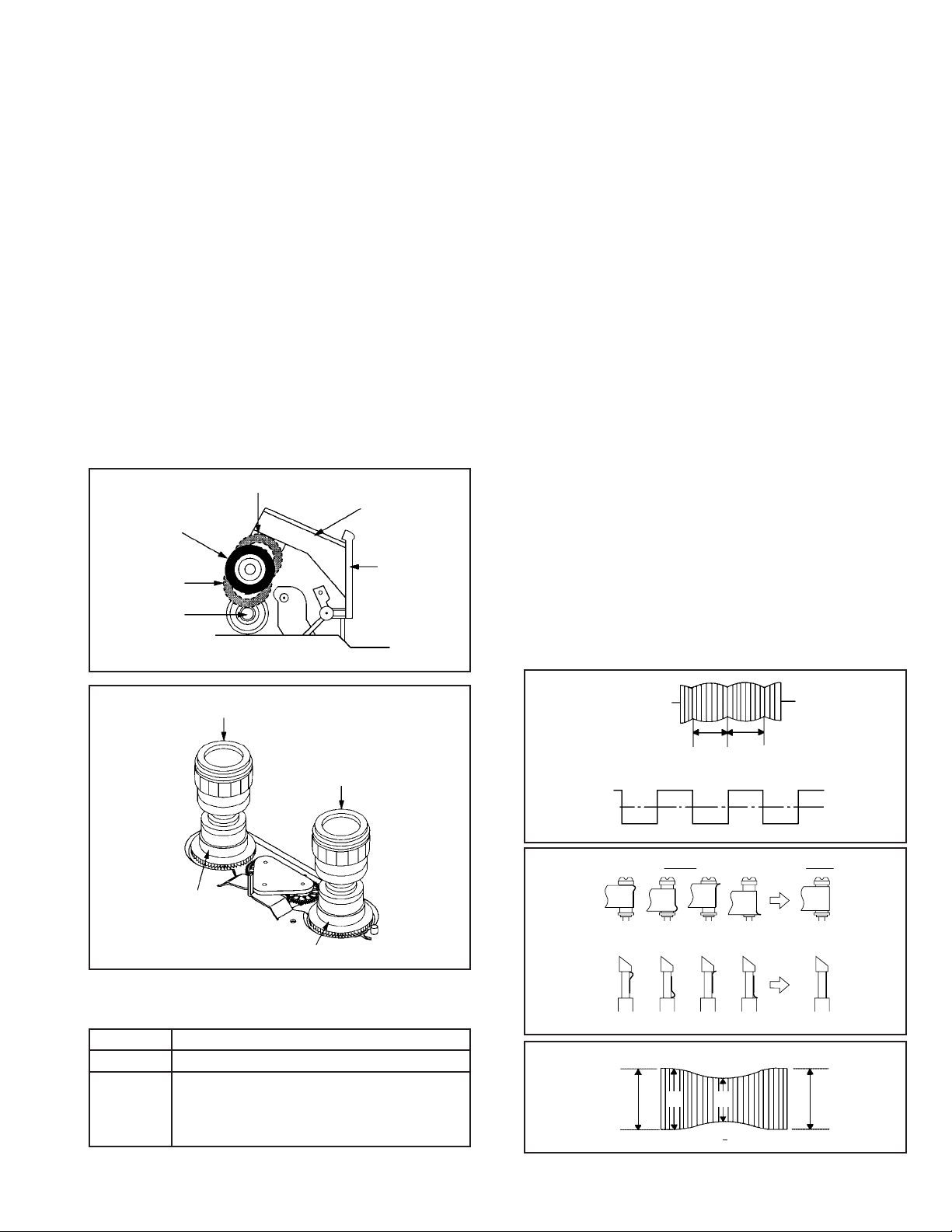
2-1: GUIDE ROLLER
Playback the VHS Alignment Tape (MHP).
1.
Connect CH-1 of the oscilloscope to TP4001 (Envelope)
2.
and CH-2 to TP1002 (SW Pulse).
Press and hold the Tracking-Auto button on the remote
3.
control more than 2 seconds to set tracking to center.
Trigger with SW Pulse and observe the envelope. (Refer
4.
to Fig. 2-1-A)
5.
When observing the envelope, adjust the Roller Driver
(PTU94002-2) slightly until the envelope will be flat.
Even if you press the Tracking Button, adjust so that
flatness is not moved so much.(Refer to Fig. 2-1-B)
6.
Adjust so that the A : B ratio is better than 3 : 2 as shown
in Fig. 2-1-C, even if you press the Tracking Button to
move the envelope (The envelope waveform will begin to
decrease when you press the Tracking Button).
7.
Adjust the SWITCHING POINT during playback.
(Refer to the ELECTRICAL ADJUSTMENTS)
NOTE
After adjustment, confirm and adjust A/C head.
(Refer to item 2-2)
Torque Gauge
Torque Gauge
S Reel
T Reel
Fig. 1-4-B
NOTE
If the torque is out of the range, replace the following parts.
Check item
1-3
1-4
S Reel side:
Replacement Part
Idler Ass’y/Clutch Ass’y
S Reel/Tension Band/Tension
Connect/Tension Arm Ass’y
T Reel side:
T Reel/T Brake Band//T Brake
Spring/T Brake Arm
CH-1
Envelope
(TP4001)
CH-2
SW Pulse (TP1002)
Improper
(a) Guide roller
(b) P4 CAP
Entrance
Max
CH-1
CH-2
Track
Track
A : B ≥ 3 : 2
Fig. 2-1-A
Proper
Fig. 2-1-B
Exit
MaxA B
Fig. 2-1-C
1-15
Page 22
MECHANICAL ADJUSTMENTS
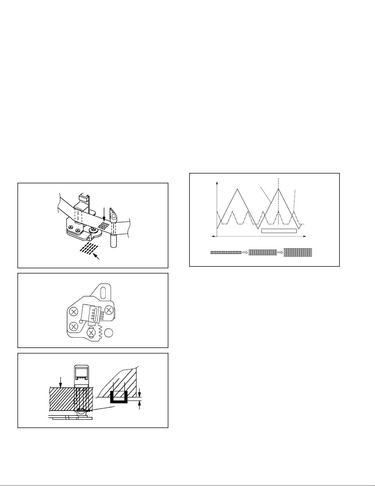
2-2: CONFIRMATION AND ADJUSTMENT OF AUDIO/
CONTROL HEAD
When the Tape Running Mechanism does not work well,
adjust the following items.
1.
Playback the VHS Alignment Tape (MHP).
2.
Confirm that the reflected picture of stamp mark is
appeared on the tape prior to P4 Post as shown in Fig. 2-
2-A.
a)
When the reflected picture is distorted, turn the screw
1 clockwise until the distortion is disappeared.
b)
When the reflected picture is not distorted, turn the
screw 1 counterclockwise until little distortion is
appeared, then adjust the a).
3.
Turn the screw 2 to set the audio level to maximum.
4.
Confirm that the bottom of the Audio/ Control Head and
the bottom of the tape is shown in Fig. 2-2-C.
c)
When the height is not correct, turn the screw 3 to
adjust the height. Then, adjust the 1~3 again.
Audio/Control Head
Reflected picture of
Stamp Mark
P4 Cap
2-3: TAPE RUNNING ADJUSTMENT
(X VALUE ADJUSTMENT)
1.
Confirm and adjust the position of the Tension Post.
(Refer to item 1-1)
2.
Adjust the Guide Roller. (Refer to item 2-1)
3.
Confirm and adjust the Audio/Control Head.
(Refer to item 2-2)
7.
Connect CH-1 of the oscilloscope to TP1002, CH-2 to
TP4001 and CH-3 to HOT side of Audio Out Jack.
5.
Playback the VHS Alignment Tape (MHP).
6.
Press and hold the Tracking-Auto button on the remote
control more than 2 seconds to set tracking to center.
7. Set the X Value adjustment driver (X-JG153) to the 4 of
Fig. 2-2-B. At first, turn the Audio/Control Head position
fully toward the capstan side. Then adjust X Value to turn
it back gradually toward the cylinder side and stop on the
second peak point position of the envelope.
Play MHP
Waveform output
X-value adjustment point
Drum side Control head position Capstan side
Play MHP-L
Audio/Control Head
3
2
Audio/Control Head
Tape
Stamp Mark
1
4
Fig. 2-2-A
Fig. 2-2-B
0.25±0.05mm
Fig. 2-2-C
Maximum
Perform tracking operation and confirm the envelope is
8.
maximum on the tracking center position.
Playback the VHS Alignment Tape(MHP-L).
9.
Perform tracking operation and confirm the envelope is
10.
maximum on the tracking center position. If envelope is
not maximum, should be fine-tune the X-VALUE.
Fig. 2-3
1-16
Page 23
ELECTRICAL ADJUSTMENTS
Read and perform this adjustment when repairing the
circuits or replacing electrical parts or PCB assemblies.
1. BASIC ADJUSTMENT
1-1: SWITCHING POINT CONDITIONS
MODE-PLAYBACK
Input Signal-Alignment Tape (MHP)
INSTRUCTIONS
Connect CH-1 on the oscilloscope to TP1002 and CH-2
1.
to TP4201.
Playback the alignment tape. (MHP)
2.
Press and hold the Tracking-Auto button on the remote
3.
control more than 2 seconds to set tracking to center.
Adjust the VR1001 until the waveform of the oscilloscope
4.
measures 6.5 ± 0.5(H) at both leading and trailing edges.
(Refer to Fig. 1-1-A, B)
CH-2
6.5H
CH-1
Fig. 1-1-A
CH-2
CH-1
6.5H
ELECTRICAL ADJUSTMENT PARTS LOCATION GUIDE
TP4201
TU6001
VR1001
Fig. 1-1-B
J4201
TP1002
TP4001
T501
J4203
J4205J4204
TP1001
SYSCON PCB
1-17
Page 24

IC DESCRIPTIONS
SYSCON PCB OEC0115A (IC1001)
No. PORT PIN NAME I/O DESCRIPRION
1 P10 SEG8 OUT LEM(LED Module) control terminal.
2 AVSS AVSS - Ground.
3 P07/AN7 BOT-H IN Tape start sensor input signal.
4 P06/AN6 HI-FI_ENV IN Input terminal of HiFi RF envelope.
5 P05/AN5 PGMM IN Input voltage from Variable Resistor of PG SHIFTER.
6 P04/AN4 MS_SEN-B IN Input terminal of mecha state sensor.
7 P03/AN3 MS_SEN-A IN
8 P02/AN2 KEY-B IN Main unit key input.
9 P01/AN1 KEY-A IN
10 P00/AN0 STEREO_SEL IN Input terminal for the judgement of voice reception condition.
11 AN-B AFT-S_CURVE IN AFT S CURVE input for tuner.
12 AN-A EOT-H IN Tape end sensor input signal.
13 AN9 SLOW OFFSET IN Terminal for the offset of Slow.
14 AN8 ENV_DET IN Input terminal of video RF envelope.
15 AVDD AVDD - ON/OFF control Micon AD section.
16 /RESET /RESET IN RESET will be done when the voltage goes to HIGH after the
reset signal.
17 P74 GND IN Ground.
18 P73 IIC CLK OUT CLOCK terminal for IIC BUS communication.
19 P72 IIC DATA OUT/IN DATA terminal for IIC BUS communication.
20 P71 Y/C CS OUT Control terminal for Y/C selection.
21 P70 CAP_FULL OUT Output the HIGH during the acceleration force of capstan motor at
SLOW mode.
22 VDD VDD - Power of CPU.
23 AUDIO_FF HI-FI H.SW OUT Output terminal of HI-FI Head SW.
24 VIDEO_FF H.SW OUT Output terminal of Video Head SW.
25 CAP_PWM CAP_PWM OUT PWM output of Capastan control.
26 DRUM_PWM DRUM_PWM OUT PWM output of Cylinder control.
27 V-PULSE DUMMY_V-SYNC OUT Virtual V Pulse output.
28 C.ROTARY C.ROTARY OUT Color Rotary Control output.
29 H.AMP.SW H.AMP.SW OUT Switching output of Head Amp SW.
30 COMP COMP IN Comparison results input of Playback Envelope level on SP/LP
heads (4 heads).
31 CTL-H(+) CTL-H(+) - Input and output terminal of Control Head.
32 CTL-H(-) CTL-H(-) - Input terminal of Control Head.
33 SV VSS SV VSS - Ground.
34 CTL_GAIN_SW CTL_GAIN_SW - Output terminal for gain.
35 CTL_AMP(-) CTL_AMP(-) - Output terminal for amp control.
36 CTL_BIAS CTL_BIAS - Output terminal for bias.
1-18
Page 25

IC DESCRIPTIONS
SYSCON PCB OEC0115A (IC1001)
No. PORT PIN NAME I/O DESCRIPRION
37 CTL_AMP CTL_AMP OUT Output terminal for amp out.
38 DFG DFG IN Input terminal for DRUM FG signal detection.
39 DPG DPG IN Input terminal for DRUM PG signal derection.
40 CFG CFG IN Input terminal for CAPSTAN FG signal detection.
41 SV VDD VCC(SV) - + 5V
42 OSD VDD VCC(OSD) - + 5V
43 CV_IN CV_IN IN Composite Video input terminal.
44 V_REF V_REF OUT
45 CV_OUT CV_OUT OUT Composite Video output.
46 CHR_BIAS CHR_BIAS IN Brightness(Brilliant)level setting of OSD character Indications.
47 AFC_LPF AFC_LPF IN Condenser connection for AFC LPF.
48 AFC_OSC AFC_OSC IN Condenser connection for AFC OSC.
49 OSD_VSS OSD_VSS - Ground.
50 DOSC_IN DOSC_IN IN Dot Clock pulse(Oscillator)of OSD character indications.
51 DOSC_OUT DOSC_OUT OUT Dot Clock pulse(Oscillator)of OSD character indications.
52 4FSC_OUT 4FSC_OUT OUT 4 FSC pulse.
53 4FSC_IN 4FSC_IN IN 4 FSC pulse.
54 SYNC SYNC IN Input terminal for composite SYNC.
55 P67/Vsync POWER_OFF_L OUT 4FSC_MUTE control output of power off.
56 P66/YC01 V_REC_ST-H OUT On control of A/V recording(Whole width erase) circuit.
57 P65/YE01 2/4 HEAD IN The initial settings of 2 head or 4 head.
58 P64/YC02 TUNER-L OUT Output low at tuner and output high at external input/play.
59 P63/YE02 A.MUTE-H OUT Mute signal of audio mute.
60 P57 CAP_FWD-H OUT Capstan forward and backward command.
61 P56 CENTER LED OUT The CENTER LED light-up/put-off control output.
62 P55 RF CH OUT OUT Switching of a RF channel.
63 P54 LDM CTL OUT Loading motor control terminal.
64 P53/TM0 POWER ON-H OUT For control the user power switch ON/OFF.
65 P52/PWM2 CYL_SPEED_UP OUT Output terminal for correct cylinder during SLOW.
66 P51/PWM1 CAP_LIMIT OUT Switch the maximum output current of the Capstan Motor.
67 P50/BUZZ SERVICE IN Input terminal for Service Mode.
68 TEST TEST IN Ground.
69 X2 X2 OUT Subclock pulse(32.768KHz)
70 X1 X1 IN
71 DVSS VSS - Ground.
72 OSC1 OSC1 IN Connect the main crystal(10MHz)
73 OSC2 OSC2 OUT
74 P47 GND - GND
75 P46 GRID5 OUT LEM(LED Module) control terminal.
Capacity connection for Sync Chip Clamp composite Video input.
1-19
Page 26

IC DESCRIPTIONS
SYSCON PCB OEC0115A (IC1001)
No. PORT PIN NAME I/O DESCRIPRION
76 P45 GRID4 OUT LEM(LED Module) control terminal.
77 P44 GRID3 OUT LEM(LED Module) control terminal.
78 P43 GRID2 OUT LEM(LED Module) control terminal.
79 P42 GRID1 OUT LEM(LED Module) control terminal.
80 P41 TAB SW IN Input terminal for judge the tape if it has TAB or not.
81 P40 POWER_ON_L OUT For control the user power switch ON/OFF.
82 P37/IC REM_IN IN Receive the remote control signal.
83 P36/NM1 CFG IN2 IN Input terminal for CAPSTAN FG signal detection.
84 P35/IRQ5 VCR-H OUT ON/OFF control of RF Modulator.
85 P34/IRQ4 SEG9 OUT LEM(LED Module) control terminal.
86 P33/IRQ3 SEG10 OUT LEM(LED Module) control terminal.
87 P32/IRQ2 REEL-T IN Input terminal of reel sensor take up.
88 P31/IRQ1 NC OUT Not used.
89 P30/IRQ0 POWER_FAIL IN Input terminal of Power fail signal.
90 P23 AC/32KHz IN
91 P22 SP-L OUT Tape speed SP mode at the time of LOW.
92 P21 EP-L OUT Tape speed EP mode at the time of LOW.
93 P20 AUDIO_OUT_MUTE OUT L for at AUDIO MUTE and POWER OFF. H for except above case.
The initial setting that is whether it does with subclock pulse or it does
the counting of the clock with an AC pulse
94 P17/PWM14 SEG1TV/CATV OUT/IN
95 P16/SCK2 SEG2 LANG SEL OUT/IN
96 P15/SI1 SEG3 INDEX OUT/IN
97 P14/S01 SEG4 OUT LEM(LED Module) control terminal.
98 P13/SCK2 SEG5 OUT LEM(LED Module) control terminal.
99 P12/SI2 SEG6 OUT LEM(LED Module) control terminal.
100 P11/SO2 SEG7 OUT LEM(LED Module) control terminal.
LEM(LED Module) control terminal.And this terminal uses it for the
initial setting of TV/CATV mode.
LEM(LED Module) control terminal.And this terminal uses it for the
initial setting of language select.
LEM(LED Module) control terminal.And this terminal uses it for the
initial setting of INDEX on/off.
1-20
Page 27
SYSCON PCB IC1001 (OEC0114A)
DPG 39 PIN
DFG 38 PIN
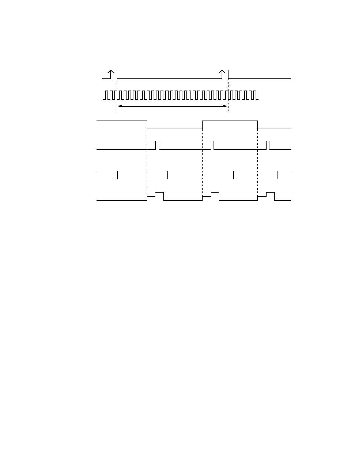
SERVO TIMING CHART
24 Cycle
H. SW. P 24 PIN
V-SYNC (E-E) 54 PIN
REC CTL (REC)
35 PIN
V-SYNC (TRICK PB)
27 PIN
• WAVEFORM CHANGES DEPENDED ON THE TAPE SPEED
CH 1
CH 2
1-21
Page 28
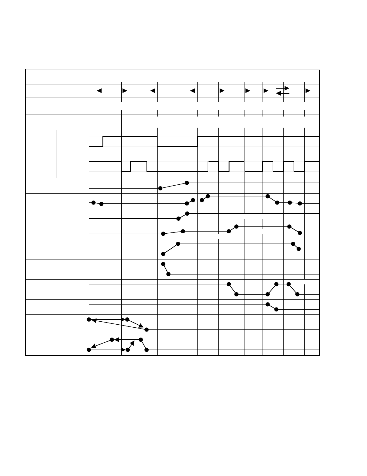
MECHANISM TIMING CHART
Please see the list below for the operational timing and the mode sensor output of the main parts on each mechanism modes.
MECHANISM MODE UNLOAD STOP3
Mode Dealing
Directions
Revolutional Angle of
MAIN CAM
Moving Quantity of
MAIN ROD (mm)
MODE MS-1
SENSOR
HIGH
LOW
EJECT
0
STBY
15
3
206.3100
180
Output
HIGH
MS-2
LOW
INCLINED BASE S/T UNIT
PINCH ROLLER BLOCK
P5 ARM ASS'Y (T BRAKE:LOW)
TENSION LEVER
TENSION ARM ASS'Y
(S REEL BRAKE)
VSR
S BRAKE:LOW
255
26.5
PRESS
PRESS
P5-ON (T BRAKE HIGH)
BRAKE-ON
PBF.SLOW
S BRAKE:HIGH
FF/REWSTOP2
323.8303.7272.2226.4
38.53529.521.5
TENSION CONNECT
(S REEL BRAKE)
T BRAKE ARM
(T REEL BRAKE)
CLUTCH LEVER
LINK UNIT
FLAP LEVER
BRAKE-ON
BRAKE-ON
CLUTCH-ON
UP
BRAKE-ON
DIRECT
PRESS
1-22
Page 29
POWER DOES NOT TURN ON
TROUBLESHOOTING GUIDE
Is the voltage at pin 15, 22,
70 of IC1001 about 5V?
No
Is the voltage at cathode
of D512 about 5V?
No
Check Around T501.
Yes
Yes
Check IC1001.
Check AT+5.2V line and the
check peripheral circuit.
1-23
Page 30

POWER SHUTS OFF
Insert a cassette and
push PLAY button.
TROUBLESHOOTING GUIDE
Does it Power off in about
3 seconds?
No
Does it Power off in about
6 seconds?
No
Does it Power off intermittently?
No
Check IC1001.
Yes
Yes
Yes
Check TAPE LOADING,
LOADING BELT, MODE SENSOR,
DD MOTOR and CYLINDER MOTOR.
Check REEL SENSOR
and REEL BELT.
Check REEL SENSOR and
REEL BELT slack.
1-24
Page 31

TROUBLESHOOTING GUIDE
CYLINDER NOT ROTATING
DURING PLAYBACK AND
RECORDING
Is the voltage at pin 11 and
12 of CP1001 about DC5V?
Yes
In playback, is the voltage
at pin 1, 4, 5 and 9 of CP1001
about DC5V?
No
Check IC1002.
CASSETTE IN AND DOWN,
UNIT HAS NO FUNCTIONS
No
Yes
Check pin 26, 38, 39 and 65
of IC1001 lines.
Replace CAPATAN DD UNIT.
Does mode OSD
appear in Monitor?
No
Does VCR operate with
the remote control?
Yes
Check Operation PCB.
Yes
No
Check LOADING MOTOR, MODE
SENSOR and the peripheral parts.
Check IC1001.
1-25
Page 32

FF/REW DO NOT WORK
TROUBLESHOOTING GUIDE
Is the voltage changing
at pin 82 of IC1001 when you
press FF/REW?
Yes
Check DECK MECHANISM.
AUDIO SHAKES
Is AUDIO HEAD scratched?
No
No
Check pins 8 and 9 of IC1001 lines.
Yes
Replace AUDIO HEAD.
Does pin 40 of IC1001
output about 5Vp-p?
Yes
In playback, is the voltage
at pin 5 of CP1001 3.0V?
Yes
Check AUDIO BLOCK.
No
No
Replace CAPSTAN DD.
Check IC1001.
1-26
Page 33

TROUBLESHOOTING GUIDE
CASSETTE TAPE IS NOT
ACCEPTED
Does WORM GEAR of
CASSETTE LOADING
BLOCK activate?
Yes
When cassette is not
inserted, is the voltage at pin
3 of IC1001 5V?
Yes
When a cassette is
inserted, is the voltage between
pins 2 and 8 of CP1001
12V?
No
When a cassette is
inserted, is the voltage at
pin 63 of IC1001 5V?
No
No
Yes
No
Check WORM GEAR of
CASSETTE LOADING BLOCK.
Check LED and PHOTO SENSOR
on DECK.
Replace LOADING MOTOR.
Replace IC1001.
Yes
Check circuit of LOADING MOTOR.
1-27
Page 34

TROUBLESHOOTING GUIDE
WHEN INSERTING CASSETTE,
IT EJECTS IMMEDIATELY
Does Another cassette go down?
No
Are SW1001 and the lever
of the stage set correctly?
Yes
After a CASSETTE is
inserted is the voltage at pin 80
of IC1001 LOW?
Yes
When CASSETTE is
inserted is the voltage at pin 3
of IC1001 5V?
Yes
No
No
No
Defective CASSETTE or
CASSETTE LOADING BLOCK.
Check Rec LEVER.
Check SW1001.
Check LOADING GEARS.
1-28
Yes
Check IC1001.
Page 35

TAPE LOADING IS OK, BUT
UNLOADS IMMEDIATELY
TROUBLESHOOTING GUIDE
Does CYLINDER rotate?
Yes
Does TP1002 feed
HEAD SWITCHING PULSE
signal?
No
No
Is the voltage at pins
11 and 12 of CP1001
UNREG 5V?
Yes
In playback, is the voltage
at pins 1,4,5 and 9 of CP1001
about 5V?
Yes
Replace CYLINDER UNIT.
No
Does PG PULSE signal
appear at pin 39 of IC1001?
No
No
Check pins 26, 38, 39
and 65 of IC1001 lines.
Replace CAPSTAN DD UNIT.
Yes
Check REEL SENSOR.
Yes
Replace IC1001.
1-29
Page 36

TROUBLESHOOTING GUIDE
CAPSTAN DD MOTOR NOT
ROTATING
In playback, is the voltage
at pin 1 of CP1001 12V?
Yes
Is the voltage at pin
3 of CP1001 5V?
Yes
In playback, check the
voltage at pin 25 of IC1001
is 2.5V?
Yes
Does DD MOTOR rotate now?
If not, replace DD MOTOR .
No
No
No
Check POWER circuit.
Replace IC1001.
1-30
Page 37

PLAYBACK PICTURE
JITTERS HORIZONTALLY
TROUBLESHOOTING GUIDE
Is FG Pulse output level
at pin 1 of CP1001 about 6V?
6V
Yes
Is the voltage at pin 83 of
IC1001 about 5V?
Yes
Replace CYLINDER MOTOR.
PLAYBACK PICTURE SHAKES
No
No
Replace CYLINDER MOTOR.
Replace IC1001.
Is FG Pulse output level
at pin 1 of CP1001 about 6V?
6V
Yes
Is the voltage at pin 4 of
CP1001 about 6V?
Yes
Replace CYLINDER MOTOR.
No
Replace CYLINDER MOTOR.
No
Replace IC1001.
1-31
Page 38

AUTO TRACKING DOES
NOT OPERATE
TROUBLESHOOTING GUIDE
By manual tracking,
does the DC level at pin 59
of IC4001 change?
Yes
In auto tracking, is the
voltage at pin 14 of IC1001
more than DC1.65V?
Yes
Replace IC1001.
WHEN PLAYBACK, FAST
FORWARD OR REWIND MODE
IS ACTIVATED, UNIT STOPS
IMMEDIATELY
No
No
Does the CTL PULSE
(about 1.0Vp-p) appear at pin 37
of IC1001?
1.0Vp-p
Yes
Check CYLINDER UNIT.
No
Check CONTROL HEAD.
1-32
Does CAPSTAN DD
MOTOR rotate?
Yes
Does the REEL SENSOR
PULSE signal appear at pins 87
and 88 IC1001?
Yes
Check IC1001 and check
peripheral circuit.
No
No
Refer to section "CAPSTAN DD
MOTOR NOTROTATING"
Check Q1002.
Page 39

TROUBLESHOOTING GUIDE
PLAYBACK PICTURE JITTERS
VERTICALLY
No Does tracking noise
appear in the picture?
Yes
By adjusting the manual
tracking UP/DOWN buttons, will the
noise disappear in the picture?
Yes
Are GUIDE POSTS
the right height?
Yes
Is PG SHIFTER Adjustment 6.5H?
Yes
No
No
No
Check P/B ENVELOPE.
Adjust GUIDE POST height.
Adjust PG SHIFTER.
Is PB-Y waveform normal?
No
Check PB-Y circuit.
Yes
Replace IC1001.
1-33
Page 40

NO PLAYBACK PICTURE
TROUBLESHOOTING GUIDE
Is E-E appearing on
the Monitor TV?
Yes
Is there Video signal
at pin 30 of IC4001?
Yes
Is there VIDEO signal
at pin 26 of IC4001?
Yes
No
No
No
Is the voltage at pin 44,
52 and 68 of IC4001 5V?
Yes
Check IC4001.
No
Check P.CON 5V line.
Check J4203.
Check IC4001 and the
peripheral circuit.
Check J4201.
1-34
Page 41

TROUBLESHOOTING GUIDE
NO PICTURE DURING PLAYBACK
Is there Video signal
at pin 26 of IC4001?
Yes
Is there Color signal
in Video signal at pin 26 of
IC4001?
Yes
Check IC4001.
NO COLOR DURING SELF
RECORDING AND PLAYBACK
No
Check IC4001.
No
Replace IC4001.
Does VIDEO signal appear
at pin 30 of IC4001?
Yes
Does VIDEO signal appear
at pin 26 of IC4001?
Yes
Check IC4001 and peripheral circuit.
No
No
Replace J4203.
Check VIDEO input circuit.
Change IC4001.
1-35
Page 42

TROUBLESHOOTING GUIDE
PLAYBACK PICTURE NOISY
(EVEN AFTER CLEANING HEADS)
Is FM signal at TP4001
more than 300mVp-p?
Yes
Is VIDEO waveform
at pin 30 of IC4001 2Vp-p
are there any noises?
Yes
Is video output at pin 26
of IC4001 2Vp-p and are
there any noise?
Yes
Check J4201.
No
No
No
Check IC4001 and CYLINDER UNIT.
Check IC4001 and peripheral circuit.
Check IC4001 and IC1001.
1-36
Page 43

NO NORMAL AUDIO
ON PLAYBACK
TROUBLESHOOTING GUIDE
Does audio appear on E-E?
Yes
Is the voltage at pin
6 of IC4001 2.3V?
Yes
Does AUDIO signal appear
at pin 10 of IC4001.
Yes
Check AUDIO HEAD for debris of
stains.
Check that the connector from
AUDIO HEAD is fully inserted to
Replace IC4001.
No
No
No
Refer to section "NO E-E".
Check C4031 and peripheral circuit.
Check IC4001 and peripheral circuit.
1-37
Page 44

AUDIO CAN NOT
BE RECORDED
TROUBLESHOOTING GUIDE
Is BIAS level O.K at
T4001?
Is there AUDIO signal
at pin 10 of IC4001?
60V
Yes
Yes
No
No
Is the voltage at Emitter
of Q4003 5V?
Yes
Is the voltage at pin 23
of IC4001 above 5V?
Yes
T4001 is broken or shorted.
No
No
Check POWER circuit.
Check IC4001.
Check the circuit between
audio out of Tuner and
pin 10 of IC4001.
Check J4201 and peripheral circuit.
1-38
Page 45

TROUBLESHOOTING GUIDE
RECORDING MECHANISM WORKS,
BUT NO VIDEO RECORDED FROM
INPUT JACK OR TUNER
Does VIDEO signal
appear at pins 30 and
32 of IC4001?
Yes
Does VIDEO signal appear
at pin 26 of IC4001?
Yes
Does FM signal appear
at pin 59 to IC4001?
No
No
No
Is the voltage at pin
56 of IC1001 5V?
Yes
Check the circuit from
VIDEO input jack to IC4001,
from Tuner Pack to IC4001.
No
Check IC1001.
Check IC4001.
Yes
Does the FM current
appear at pin 59 of IC4001
during the REC?
Yes
Check CYLINDER UNIT and
IC4001 circuit.
No
Check IC4001 and check
the peripheral circuit.
1-39
Page 46

NO E-E
(NO VIDEO FROM TUNER)
TROUBLESHOOTING GUIDE
Are the plugs
connected to the
VIDEO input jacks?
Yes
Do the voltages appear at
each terminal +B(5V), PB(5V)
and TU(32V) of TU6001?
Yes
Check VIDEO
Does VIDEO signal
appear at pin 24 of
TU6001?
No
No
No
Disconnect the plugs from the
VIDEO input Jacks.
Check peripheral circuit.
Replace TU6001.
Yes
Is there VIDEO
waveform at pin
32 of IC4001?
Yes
Replace IC4001.
No
Check J4201.
1-40
Page 47

NO E-E AUDIO (MONO)
TROUBLESHOOTING GUIDE
Is the voltage at pins 52, 68
and 77 of IC4001 5V?
Yes
Does signal appear
at pin 78 of IC4001?
Yes
Does signal appear
at pin 10 of IC4001?
Yes
Check J4201.
No
No
No
Check POWER BLOCK.
Check J4204 and J4205.
Replace IC4001.
1-41
Page 48

NO TUNER AUDIO (MONO)
TROUBLESHOOTING GUIDE
Do the voltages appear at
each terminal +B(5V), PB(5V)
and TU(32V) of TU6001?
Yes
Does signal appear
at pin 22 of TU6001?
Yes
Does signal appear
at pin 76 of IC4001?
Yes
Check J4201 and peripheral circuit.
No
Check POWER BLOCK.
No
Check TU6001 and peripheral circuit.
No
Replace IC4001.
1-42
Page 49

<Reference>
GENERAL SPECIFICATIONS [HR-A591U/A591U(C)]
G-1 VCR System VHS Player / Recorder
G-2 Tuning Broadcasting System US System M
G-3 Power Power Source AC 120V,60Hz
G-4 Regulation Safety UL / CSA
G-5 Temperature Operation 5oC - 40oC
G-6 Operating Humidity Less then 80% RH
G-7 Signal Video Signal Input Level 1 V p-p/75 ohm
System Video System NTSC
System Tuner and System 1Tuner
Hi-Fi STEREO Yes
NTSC PB(PAL60Hz) No
Deck DECK OVD-7
Heads Video Head 4Head
FM Audio Head 2Head
Normal Audio /Control Mono / Yes
Erase(Full Track Erase) Yes
Tape Rec PAL Speed NTSC SP/EP(SLP)
Play PAL -
Fast Forward / Rewind Time (Approx.) FF:4'50"/REW:2'30"
Forward/Reverse NTSC or PAL-M SP/EP(SLP)=3x,5x/9x,15x
Picture Search PAL or SECAM Frame Advance 1/10
Slow Speed 1/10
Receive CH Destination USA(w/CATV)
Intermediate Picture(FP) 45.75MHz
Frequency Sound(FS) 41.25MHz
Preset CH No
RF Converter Output Yes
Channel 3 or 4 ch
Level/Impedance 66dBu /75ohm
Sound Selector No
Stereo/Dual TV Sound Yes(US-ST)
Power Consumption Power On(at AC) 9W at 120V 60Hz
Protector Power Fuse Yes
Audio Signal Input Level -8dBm/50Kohm
Hi-Fi Audio Signal Dynamic Range : More than 90dB
Loading System Front
Motor 3
NTSC SP/EP(SLP)
with Cassette T-120
Tuning System F-Synth
Input Impedance VHF/UHF 75 OHM
CH Coverage
FP-FS 4.50MHz
DC -
Stand by (at AC) 1.7W at 120V 60Hz
Per Year - kWh/Year
Dew Sensor No
Radiation FCC / DOC
Storage -20oC - 60oC
Output Level 1 V p-p/75 ohm
S/N Ratio (Weighted) 50
Horizontal Resolution at SP Mode 230Line
Output Level -8dBm/1Kohm
S/N Ratio at SP (Weighted) 42dB
Harmonic Distortion at SP(1KHz) typ. 1.5%
Frequency Response at SP 100Hz - 10kHz
at LP -
at SLP 100Hz - 4kHz
Frequency Response 20Hz ~20kHz
Wow And Flutter : Less than 0.01 %Wrms
Channel Separation : More than 60 dB
Harmonic Distortion : Less than 0.01
2-69,4A,A-5~ A-1,A~I,J~ W
W+1-W+84
4-1
Page 50

,FF(
GENERAL SPECIFICATIONS [HR-A591U/A591U(C)]
G-8 On Screen Menu Yes
G-9 OSD Language English French Spanish
G-10 Clock,Timer Calendar 1990/1/1 ~ 2081/12/31
G-11 Display Indicator Yes
Display Menu Type Character
G-CODE(or SHOWVIEW or PLUSCODE)No. Entry No
NICAM 1/2,NICAM Off,Audio Output No
Stereo,Audio Output,SAP Yes
Play/Stop/FF/Rew/Rec/OTR/T-Rec/Pause/Eject/Tape In (Symbol Mark)
and Timer Timer Events 8 prog/1 month
Back-up One Touch Recording Max Time 5 Hours
OTPB Valid Time No
Timer Back-up (at Power Off Mode) 5 sec.
Indicator Type LED Module(Amber + Red)
ATS No
Timer Rec Set Yes
Auto Repeat On/Off Yes
SAP On Off Yes
CH Set-Up Yes
Pin Code Registration No
System Set-Up No
Clock Set Yes (Calendar 12H)
Language Yes
No Noise Back Ground Yes
OSD Language Setting English
TV/CATV Yes
Auto CH Memory Yes
Add/Delete Yes
CH/AV Yes
Clock Yes
Repeat Yes
Pin Code No
Tape Counter Yes
Index No
Hotel Lock No
Tape Speed Yes
Manual Tracking (Bar Setting) No
Hi-Fi Yes
S-Repeat/SR-R/SR-Play No
VPS No
PDC No
Clock/Counter,CH,Timer Rec,OTR, Play
Rec
Cue),Rew(Rev),Stop,ATR
Pause Yes
Still Yes
Eject(Tape Mark Flash) Yes
Slow Yes
WKL,Y.M.D,Start,End No
AFT No
Repeat No
A-DUB No
VCR Yes
Memory No
Index No
VPS No
PDC No
SP No
LP No
SLP No
AM No
PM Yes
F1,F2
RF Output CH Yes
Tape In Yes
Yes
Yes
No
4-2
Page 51

GENERAL SPECIFICATIONS [HR-A591U/A591U(C)]
G-12 Remote Unit RC-ES
Control Glow in Dark Remocon No
Format type JVC
Custom Code 43 / 03
Power Source Voltage(D.C) 3V
UM size x pcs UM-4 x 2 pcs
Total Keys 35 Keys
Keys Power Yes
1 Yes
2 Yes
3 Yes
4 Yes
5 Yes
6 Yes
7 Yes
8 Yes
9 Yes
0/Input Select Yes
CH Up Yes
CH Down Yes
Input Select No
Play /Slow Yes
F.Fwd Yes
Rew Yes
Pause/Still Yes
Stop Yes
Rec/OTR Yes
Eject No
Counter Reset/Cancel Yes
Speed / Auto Tracking Yes
Timer Rec Yes
TV Monitor No
Quick View No
Program No
Slow No
Auto Tracking No
Set/Tracking+ Yes
Set/ Tracking - Yes
Menu Yes
Enter Yes
Cancel No
Display(Clock/Counter+Call) Yes
TV/VCR Yes
Sleep Timer No
Muting No
Clock/Counter No
Zero Return No
CM Skip No
Audio Select Yes
TV CH+ Yes
TV CH- Yes
TV Input Select Yes
TV Volume+ Yes
TV Volume- Yes
TV Power Yes
4-3
Page 52

GENERAL SPECIFICATIONS [HR-A591U/A591U(C)]
G-13 Features Auto Head Cleaning No
G-14 Accessories Owner's Manual Language English French(A591U(C))
Auto Tracking Yes
Index Search No
HQ (VHS Standard High Quality) Yes
Auto Power On, Auto Play, Auto Rewind, Auto Eject Yes
Auto Power Off Yes
Forward/Reverse Picture Search Yes
VIDEO PLUS+(SHOWVIEW,G-CODE) No
ATS No
PDC No
VPS No
One Touch Playback No
Picture Control No
Auto CH Memory Yes
Channel Lock No
Hotel Lock No
Anti Theft No
Audio Dubbing No
Remort Control Code 1/2 No
SQPB Yes
CATV Yes
Energy Star Yes
MTS(SAP) Yes
CM Skip(30sec x 6 Times) No
w/Guarantee Card Yes
Remote Control Unit Yes
Dew Cation Sheet No
Video Cassette Tape No
Battery Yes
UM size x pcs UM 4 x 2pcs
Safety Tip No
Toll Free Insert Sheet No
Quick Set-Up Sheet No
Information Sheet (Buyer Supply) No
75 Ohm Coaxial Cable Yes
Rod Antenna No
Poles
Terminal
Loop Antenna No
Terminal
U/V Mixer No
DC Car Cord (Center+) No
Guarantee Card No
Warning Sheet No
Circuit Diagram No
Antenna Change Plug No
Service Facility List No
Important Safeguard No
Dew/AHC Caution Sheet No
AC Plug Adapter No
Quick Set-up Sheet No
AC Cord No
AV Cord No
Product Registration Card Yes (Buyer's Supply)
PTB Sheet No
Tape Rewinder(Buyer Supply) No
300 ohm to 75 ohm Antenna Adapter No
4-4
Page 53

GENERAL SPECIFICATIONS [HR-A591U/A591U(C)]
G-15 Interface Switch Front Power Yes
Rear RF Output SW No
Indicator Power No
Terminals Front Video Input RCA x 1 (Black)
Rear Video Input No
G-16 Set Size Approx. W x D x H (mm) 360 x 224 x 95
G-17 Weight Net (Approx.) 3.2kg(7.1lbs)
G-18 Carton Master Carton No
Gift Box Yes
Drop Test Natural Dropping At 1Corner / 3Edges / 6Surfaces
Container Stuffing(40' container) 3136Sets
G-19 Cabinet Material Cabinet Front PS 94V2 or More / DECABROM
Play Yes
Pause/Still No
System Select No
One Touch Playback No
Channel Up Yes
Channel Down Yes
F.FWD/Cue Yes
Eject/Stop Yes
Main Power SW No
Volume Up No
Volume Down No
Rew/Rev Yes
Rec/OTR Yes
Stand by No
Repeat No
TV/VCR No
Rec No
T-Rec No
Tape In No
Audio Input RCA x 2 (Stereo, Black)
Other Terminal No
Audio Input No
Video Output RCA x 1 (Yellow)
Audio Output RCA x 2 (Stereo, White/Red)
Euro Scart No
DC Jack 12V(Center +) No
VHF/UHF Antenna Input F Type
AC Inlet No
Gross (Approx.) 3.8kg(8.4lbs)
Content Material Dimensions W x D x H(mm) Description of Origin -
Material Single/White
Dimensions W x D x H(mm) 420x291x160
Design As Per BUYER 's
Description of Origin Yes
Height (cm) 80
4-5
Page 54

GENERAL SPECIFICATIONS [HR-A590U(C)]
G-1 VCR System VHS Player / Recorder
System Video System NTSC
G-2 Tuning Broadcasting System US System M
System Tuner and System 1Tuner
G-3 Power Power Source AC 120V,60Hz
G-4 Regulation Safety UL / CSA
G-5 Temperature Operation 5oC - 40oC
G-6 Operating Humidity Less then 80% RH
G-7 Signal Video Signal Input Level 1 V p-p/75 ohm
Hi-Fi STEREO Yes
NTSC PB(PAL60Hz) No
Deck DECK OVD-7
Heads Video Head 4Head
FM Audio Head 2Head
Normal Audio /Control Mono / Yes
Erase(Full Track Erase) Yes
Tape Rec PAL Speed NTSC SP/EP(SLP)
Play PAL Fast Forward / Rewind Time (Approx.) FF:4'50"/REW:2'30"
Forward/Reverse NTSC or PAL-M SP/EP(SLP)=3x,5x/9x,15x
Picture Search PAL or SECAM Frame Advance 1/10
Slow Speed 1/10
Receive CH Destination USA(w/CATV)
Intermediate Picture(FP) 45.75MHz
Frequency Sound(FS) 41.25MHz
Preset CH No
RF Converter Output Yes
Channel 3 or 4 ch
Level/Impedance 66dBu /75ohm
Sound Selector No
Stereo/Dual TV Sound Yes(US-ST)
Power Consumption Power On(at AC) 9W at 120V 60Hz
Protector Power Fuse Yes
Audio Signal Input Level -8dBm/50Kohm
(0dB=0.775Vrms) Output Level -8dBm/1Kohm
Hi-Fi Audio Signal Dynamic Range : More than 90dB
Loading System Front
Motor 3
NTSC SP/EP(SLP)
with Cassette T-120
Tuning System F-Synth
Input Impedance VHF/UHF 75 OHM
CH Coverage
FP-FS 4.50MHz
DC Stand by (at AC) 1.7W at 120V 60Hz
Per Year - kWh/Year
Dew Sensor No
Radiation FCC / DOC
Storage -20oC - 60oC
Output Level 1 V p-p/75 ohm
S/N Ratio (Weighted) 50
Horizontal Resolution at SP Mode 230Line
S/N Ratio at SP (Weighted) 42dB
Harmonic Distortion (1KHz) 1.5%
Frequency Response at SP 100Hz - 10kHz
at LP -
at SLP 100Hz - 4kHz
Frequency Response 20Hz ~20kHz
Wow And Flutter : Less than 0.01 %Wrms
Channel Separation : More than 60 dB
Harmonic Distortion : Less than 0.01
2-69,4A,A-5~ A-1,A~I,J~ W
W+1-W+84
4-6
Page 55

y
)
,FF(
GENERAL SPECIFICATIONS [HR-A590U(C)]
G-8 On Screen Menu Yes
Display Menu Type Character
G-CODE(or SHOWVIEW or PLUSCODE)No. Entry No
NICAM 1/2,NICAM Off,Audio Output No
Stereo,Audio Output,SAP Yes
Pla
/Stop/FF/Rew/Rec/OTR/T-Rec/Pause/Eject/Tape In (Symbol Mark
G-9 OSD Language English French Spanish
G-10 Clock,Timer Calendar 1990/1/1 ~ 2081/12/31
and Timer Timer Events 8 prog/1 month
Back-up One Touch Recording Max Time 5 Hours
G-11 Display Indicator No
OTPB Valid Time No
Timer Back-up (at Power Off Mode) 5 sec.
Indicator Type -
ATS No
Timer Rec Set Yes
Auto Repeat On/Off Yes
SAP On Off Yes
CH Set-Up Yes
Pin Code Registration No
System Set-Up No
Clock Set Yes (Calendar 12H)
Language Yes
No Noise Back Ground Yes
OSD Language Setting English
Clock/Counter,CH,Timer Rec,OTR, Play
TV/CATV Yes
Auto CH Memory Yes
Add/Delete Yes
CH/AV Yes
Clock Yes
Repeat Yes
Pin Code No
Tape Counter Yes
Index No
Hotel Lock No
Tape Speed Yes
Manual Tracking (Bar Setting) No
Hi-Fi Yes
S-Repeat/SR-R/SR-Play No
VPS No
PDC No
Rec
Cue),Rew(Rev),Stop,ATR
Pause Still Eject(Tape Mark Flash) Slow WKL,Y.M.D,Start,End AFT Repeat A-DUB VCR Memory Index VPS PDC SP LP SLP AM PM -
F1,F2
RF Output CH -
Tape In -
Yes
-
-
4-7
Page 56

GENERAL SPECIFICATIONS [HR-A590U(C)]
G-12 Remote Unit RC-ES
Control Glow in Dark Remocon No
Format type JVC
Custom Code 43 / 03
Power Source Voltage(D.C) 3V
UM size x pcs UM-4 x 2 pcs
Total Keys 35 Keys
Keys Power Yes
1 Yes
2 Yes
3 Yes
4 Yes
5 Yes
6 Yes
7 Yes
8 Yes
9 Yes
0/Input Select Yes
CH Up Yes
CH Down Yes
Input Select No
Play/Slow Yes
F.Fwd Yes
Rew Yes
Pause/Still Yes
Stop Yes
Rec/OTR Yes
Eject No
Counter Reset/Cancel Yes
Speed / Auto Tracking Yes
Timer Rec Yes
TV Monitor No
Quick View No
Program No
Slow No
Auto Tracking No
Set/Tracking+ Yes
Set/ Tracking - Yes
Menu Yes
Enter Yes
Cancel No
Display(Call) Yes
TV/VCR Yes
Sleep Timer No
Muting No
Clock/Counter No
Zero Return No
CM Skip No
Audio Select Yes
TV CH+ Yes
TV CH- Yes
TV Input Select Yes
TV Volume+ Yes
TV Volume- Yes
TV Power Yes
4-8
Page 57

GENERAL SPECIFICATIONS [HR-A590U(C)]
G-13 Features Auto Head Cleaning No
G-14 Accessories Owner's Manual Language English / French
Auto Tracking Yes
Index Search No
HQ (VHS Standard High Quality) Yes
Auto Power On, Auto Play, Auto Rewind, Auto Eject Yes
Auto Power Off Yes
Forward/Reverse Picture Search Yes
VIDEO PLUS+(SHOWVIEW,G-CODE) No
ATS No
PDC No
VPS No
One Touch Playback No
Picture Control No
Auto CH Memory Yes
Channel Lock No
Hotel Lock No
Anti Theft No
Audio Dubbing No
Remort Control Code 1/2 No
SQPB Yes
CATV Yes
Energy Star Yes
MTS(SAP) Yes
CM Skip(30sec x 6 Times) No
w/Guarantee Card No
Remote Control Unit Yes
Dew Cation Sheet No
Video Cassette Tape No
Battery Yes
UM size x pcs UM 4 x 2pcs
Safety Tip No
Toll Free Insert Sheet No
Quick Set-Up Sheet No
Information Sheet (Buyer Supply) No
75 Ohm Coaxial Cable Yes
Rod Antenna No
Poles
Terminal
Loop Antenna No
Terminal
U/V Mixer No
DC Car Cord (Center+) No
Guarantee Card Yes
Warning Sheet No
Circuit Diagram No
Antenna Change Plug No
Service Station List Yes
Important Safeguard No
Dew/AHC Caution Sheet No
AC Plug Adapter No
Quick Set-up Sheet No
AC Cord No
AV Cord No
Registration Card No
PTB Sheet No
Tape Rewinder(Buyer Supply) No
300 ohm to 75 ohm Antenna Adapter No
4-9
Page 58

GENERAL SPECIFICATIONS [HR-A590U(C)]
G-15 Interface Switch Front Power Yes
Rear RF Output SW Yes
Indicator Power
Terminals Front Video Input RCA x 1 (Black)
Rear Video Input No
G-16 Set Size Approx. W x D x H (mm) 360 x 224 x 95
G-17 Weight Net (Approx.) 3.2kg(7.1lbs)
G-18 Carton Master Carton No
Gift Box Yes
Drop Test Natural Dropping At 1Corner / 3Edges / 6Surfaces
Container Stuffing(40' container) 3136Sets
G-19 Cabinet Material Cabinet Front PS 94V2 or More / DEC
Play Yes
Pause/Still No
System Select No
One Touch Playback No
Channel Up Yes
Channel Down Yes
F.FWD/Cue Yes
Eject/Stop Yes
Main Power SW No
Volume Up No
Volume Down No
Rew/Rev Yes
Rec/OTR Yes
Yes(Green)
Stand by No
Repeat No
TV/VCR
Rec Yes(Red)
T-Rec Yes(Red)
Tape In No
Audio Input RCA x 2 (Stereo,Black)
Other Terminal No
Audio Input No
Video Output RCA x 1 (Yellow)
Audio Output RCA x 2 (Stereo, White/Red)
Euro Scart No
DC Jack 12V(Center +) No
VHF/UHF Antenna Input/Output F Type
AC Inlet No
Gross (Approx.) 3.8kg(8.4lbs)
Content -
Material Dimensions W x D x H(mm) Description of Origin -
Material Single/White
Dimensions W x D x H(mm) 420x291x160
Design As Per BUYER 's
Description of Origin Yes
Height (cm) 80
Yes(Green)
4-10
Page 59

Page 60

JVC SERVICE & ENGINEERING COMPANY OF AMERICA
DIVISION OF JVC AMERICAS CORP.
Head office
East Coast
Midwest
West Coast
Atlanta
Hawaii
Head office
Montreal
Vancouver
:
1700 Valley Road Wayne, New Jersey 07470-9976
10 New Maple Avenue Pine Brook, New Jersey 07058-9641
:
705 Enterprise Street Aurora, Illinois 60504-8149
:
5665 Corporate Avenue Cypress, California 90630-0024
:
1500 Lakes Parkway Lawrenceville, Georgia 30043-5857
:
2969 Mapunapuna Place Honolulu, Hawaii 96819-2040
:
JVC CANADA INC.
:
21 Finchdene Square Scarborough, Ontario M1X 1A7
:
16800 Rte Trans-Canadienne, Kirkland, Quebec H9H 5G7
:
13040 Worster Court Richmond, B.C. V6V 2B3
(973)317-5000
(973)396-1000
(630)851-7855
(714)229-8011
(770)339-2582
(808)833-5828
(416)293-1311
(514)871-1311
(604)270-1311
S40895-04
Printed in Japan
Page 61

VIDEO CASSETTE RECORDER
HR-A591U
INSTRUCTIONS
LPT0661-001B
COPYRIGHT © 2002 VICTOR COMPANY OF JAPAN, LTD.
Dear Customer,
Thank you for purchasing the JVC VHS video cassette recorder.
Before use, please read the safety information and precautions to
ensure safe use of your new VCR.
CAUTIONS
The lightning flash with arrowhead symbol, within
an equilateral triangle, is intended to alert the user
to the presence of uninsulated “dangerous voltage”
within the product’s enclosure that may be of
sufficient magnitude to constitute a risk of electric
shock to persons.
The exclamation point within an equilateral triangle
is intended to alert the user to the presence of
important operating and maintenance (servicing)
instructions in the literature accompanying the
appliance.
Printed in Thailand
4 F2 1601 B
K
02/01
CAUTION:
Changes or modifications not approved by JVC could void user’s
authority to operate the equipment.
Failure to heed the following precautions may result in damage
to the VCR, Remote or video cassette.
1 DO NOT place the VCR . . .
...in an environment prone to extreme temperatures or humidity.
...in direct sunlight.
...in a dusty environment.
...in an environment where strong magnetic fields are generated.
...on a surface that is unstable or subject to vibration.
2. DO NOT block the VCR’s ventilation openings.
3. DO NOT place heavy objects on the VCR or on the Remote.
4. DO NOT place anything which might spill on the top of the VCR
or on the Remote.
5. AVOID violent shocks to the VCR during transport.
For Customer Use:
Enter below the Model No. and Serial No. which are located
on the rear of cabinet. Retain this information for future
reference.
Model No.
Serial No.
WARNING:
TO PREVENT FIRE OR SHOCK HAZARD, DO NOT EXPOSE
THIS UNIT TO RAIN OR MOISTURE.
CAUTION:
This video cassette recorder should be used with AC 120V~,
60Hz only.
To prevent electric shocks and fire hazards, DO NOT use any
other power source.
CAUTION:
TO PREVENT ELECTRIC SHOCK, MATCH WIDE BLADE OF PLUG
TO WIDE SLOT, FULLY INSERT.
ATTENTION:
POUR ÉVITER LES CHOCS ÉLECTRIQUES, INTRODUIRE LA
LAME LA PLUS LARGE DE LA FICHE DANS LA BORNE
CORRESPONDANTE DE LA PRISE ET POUSSER JUSQU’AU
FOND.
Note to CATV system installer:
This reminder is provided to call the CATV system installer’s
attention to Article 820-40 of the NEC that provides guidelines
for proper grounding and, in particular, specifies that the cable
ground shall be connected to the grounding system of the
building, as close to the point of cable entry as practical.
• Cassettes marked “VHS” (or “S-VHS”) can be used with this video
cassette recorder. However, S-VHS recording is not possible with
this model.
• This model is equipped with SQPB (S-VHS QUASI PLAYBACK)
that makes it possible to play back S-VHS recordings with
regular VHS resolution.
• HQ VHS is compatible with existing VHS equipment.
• As an Energy Star® Partner, JVC has determined that this
product or product model meets the Energy Star® guidelines for
energy efficiency.
Page 62

IMPORTANT PRODUCT SAFETY
INSTRUCTIONS
Electrical energy can perform many useful functions. But improper
use can result in potential electrical shock or fire hazards. This
product has been engineered and manufactured to assure your
personal safety. In order not to defeat the built-in safeguards,
observe the following basic rules for its installation, use and
servicing.
ATTENTION:
Follow and obey all warnings and instructions marked on your
product and its operating instructions. For your safety, please read
all the safety and operating instructions before you operate this
product and keep this booklet for future reference.
INSTALLATION
1. Grounding or Polarization
(A) Your product may be equipped with a polarized alternating-
current line plug (a plug having one blade wider than the other).
This plug will fit into the power outlet only one way. This is a
safety feature.
If you are unable to insert the plug fully into the outlet, try
reversing the plug. If the plug should still fail to fit, contact your
electrician to replace your obsolete outlet. Do not defeat the
safety purpose of the polarized plug.
(B) Your product may be equipped with a 3-wire grounding-type
plug, a plug having a third (grounding) pin. This plug will only fit
into a grounding-type power outlet. This is a safety feature.
If you are unable to insert the plug into the outlet, contact your
electrician to replace your obsolete outlet. Do not defeat the
safety purpose of the grounding-type plug.
2. Power Sources
Operate your product only from the type of power source indicated
on the marking label. If you are not sure of the type of power supply
to your home, consult your product dealer or local power company.
If your product is intended to operate from battery power, or other
sources, refer to the operating instructions.
3. Overloading
Do not overload wall outlets, extension cords, or integral
convenience receptacles as this can result in a risk of fire or electric
shock.
4. Power Cord Protection
Power supply cords should be routed so that they are not likely to
be walked on or pinched by items placed upon or against them,
paying particular attention to cords at plugs, convenience
receptacles, and the point where they exit from the product.
5. Ventilation
Slots and openings in the cabinet are provided for ventilation. To
ensure reliable operation of the product and to protect it from
overheating, these openings must not be blocked or covered.
• Do not block the openings by placing the product on a bed, sofa,
rug or other similar surface.
• Do not place the product in a built-in installation such as a
bookcase or rack unless proper ventilation is provided or the
manufacturer’s instructions have been adhered to.
6. Wall or Ceiling Mounting
The product should be mounted to a wall or ceiling only as
recommended by the manufacturer.
ANTENNA INSTALLATION INSTRUCTIONS
1. Outdoor Antenna Grounding
If an outside antenna or cable system is connected to the product,
be sure the antenna or cable system is grounded so as to provide
some protection against voltage surges and built-up static charges.
Article 810 of the National Electrical Code, ANSI/NFPA 70, provides
information with regard to proper grounding of the mast and
supporting structure, grounding of the lead-in wire to an antenna
discharge unit, size of grounding connectors, location of antenna
discharge unit, connection to grounding electrodes, and
requirements for the grounding electrode.
2. Lightning
For added protection for this product during a lightning storm, or
when it is left unattended and unused for long periods of time,
unplug it from the wall outlet and disconnect the antenna or cable
system. This will prevent damage to the product due to lightning and
power-line surges.
3. Power Lines
An outside antenna
system should not be
located in the vicinity of
overhead power lines
or other electric light or
power circuits, or where
it can fall into such
power lines or circuits.
When installing an
outside antenna system,
extreme care should be
taken to keep from
touching such power
lines or circuits as
contact with them might
be fatal.
USE
1. Accessories
To avoid personal injury:
• Do not place this product on an unstable cart, stand, tripod,
bracket, or table. It may fall, causing serious injury to a child or
adult, and serious damage to the product.
• Use only with a cart, stand, tripod, bracket, or table recommended
by the manufacturer or sold with the product.
• Use a mounting accessory recommended by the manufacturer
and follow the manufacturer’s instructions for any mounting of
the product.
• Do not try to roll a cart with small casters across thresholds or
deep-pile carpets.
2. Product and Cart Combination
A product and cart combination should be
moved with care. Quick stops, excessive
force, and uneven surfaces may cause the
product and cart combination to overturn.
3. Water and Moisture
Do not use this product near water—for
example, near a bath tub, wash bowl,
kitchen sink or laundry tub, in a wet
basement, or near a swimming pool and
the like.
4. Object and Liquid Entry
Never push objects of any kind into this product through openings
as they may touch dangerous voltage points or short-out parts that
could result in a fire or electric shock. Never spill liquid of any kind
on the product.
5. Attachments
Do not use attachments not recommended by the manufacturer of
this product as they may cause hazards.
6. Cleaning
Unplug this product from the wall outlet before cleaning. Do not use
liquid cleaners or aerosol cleaners. Use a damp cloth for cleaning.
7. Heat
The product should be situated away from heat sources such as
radiators, heat registers, stoves, or other products (including
amplifiers) that produce heat.
SERVICING
1. Servicing
If your product is not operating correctly or exhibits a marked
change in performance and you are unable to restore normal
operation by following the detailed procedure in its operating
instructions, do not attempt to service it yourself as opening or
removing covers may expose you to dangerous voltage or other
hazards. Refer all servicing to qualified service personnel.
2. Damage Requiring Service
Unplug this product from the wall outlet and refer servicing to
qualified service personnel under the following conditions:
a. When the power supply cord or plug is damaged.
b. If liquid has been spilled, or objects have fallen into the product.
c. If the product has been exposed to rain or water.
Page 63

d. If the product does not operate normally by following the
operating instructions. Adjust only those controls that are
covered by the operating instructions as an improper
adjustment of other controls may result in damage and will
often require extensive work by a qualified technician to restore
the product to its normal operation.
e. If the product has been dropped or damaged in any way.
f. When the product exhibits a distinct change in performance—
this indicates a need for service.
3. Replacement Parts
When replacement parts are required, be sure the service technician
has used replacement parts specified by the manufacturer or which
have the same characteristics as the original part. Unauthorized
substitutions may result in fire, electric shock or other hazards.
4. Safety Check
Upon completion of any service or repairs to this product, ask the
service technician to perform safety checks to determine that the
product is in safe operating condition.
How to use the Remote
Before use, insert two AAA size batteries into the Remote with the
polarity ( and ) matched correctly as indicated on the battery
compartment or on the lid.
• Point the Remote toward the remote sensor on the target
component.
• The maximum operating distance of the remote control is about 5
m.
NOTE:
If the Remote does not work properly, remove its batteries, wait for a
few seconds, replace the batteries and then try again.
Video heads cleaning
Use a dry cleaning cassette — TCL-2— when:
• Rough, poor picture appears while a tape is played back.
• The picture is unclear or no picture appears.
Buttons, Connectors and Indicators
Front Panel
VIDEO (MONO) L – AUDIO – R
VIDEO/AUDIO
input connectors
Display Panel
One-touch Timer Recording
Timer
Record
Tape In
POWER
STOP/EJECT
Cassette loading slot
POWER
Remote
sensor
Multi-Function Display
STOP/EJECT
CH
CH–/+
REC
REC
REW
PLAY
PLAY
REW
FF
FF
VCR
ATR (Auto
Tracking)
AM/PM
Rear Panel
AC power cord
UHF/VHF IN (ANT)
OUT
VIDEO
L
AUDIO
R
AUDIO/VIDEO OUT
UHF/VHF OUT (TV)
UHF/VHF
IN(ANT)
OUT(TV)
Page 64

– Buttons, Connectors and Indicators –
UHF/VHF
OUT(TV)
IN(ANT)
VIDEO
OUT
AUDIO
L
R
UHF/VHF
OUT(TV)
IN(ANT)
VIDEO
OUT
AUDIO
L
R
Remote
POWER
POWER
123
Number keys
AUX
REC
456
7089
CH(AUX)
–
REC
PLAY
REW
STOP
MENU
SET–/+
TV/VCR
A.MONITOR
TV POWER
REW FF
MENU
STOP
+
–
SET
TV/VCR TIMER
A.MONITOR SP/EP DISPLAY
–
INPUT
TV CH
–
TV VOL
TV POWER
INPUT
TV VOL–/+
This Remote transmit A code
signals only; it is not applicable
to B code signals.
PAUSE
ENTER
CANCEL
C.RESET
+
+
Connections and VCR channel
Setting
Check contents
1
Make sure the package contains all of the accessories listed
CH–/+
+
PAUSE
PLAY
FF
ENTER
TIMER
CANCEL
C.RESET
SP/EP
DISPLAY
TV CH–/+
in “Specifications”.
2
Situate VCR
Place the VCR on a stable, horizontal surface.
Connect VCR to TV
3
Antenna or cable
Coaxial cable
Flat feeder
Matching transformer
(not supplied)
AC power cord
Back of VCR
AC outlet
On-screen display
If you press DISPLAY on the Remote, you can see the current VCR
status on the TV screen. Press DISPLAY again to exit on-screen
display.
The indications are not recorded even if the VCR is in the recording
mode.
WHILE WATCHING TV
DAY AND CLOCK TIME
STEREO AND
SEPARATE AUDIO
PROGRAM (SAP)
OUTPUT
SELECTION
WHILE OPERATING A TAPE
HI-FI STEREO
AUTO TRACKING
OUTPUT
SELECTION
STEREO SAP
STEREO
HI-FI
AUTO TR.
STEREO
CH 1258 : 30 AM THU
00 : 00 : 00 SP
00 : 00 : 00 SP
REAL TIME COUNTER
OPERATING MODE
CH 1258 : 30 AM THU
CHANNEL
TAPE
SPEED
AUTO REPEAT
TAPE IN
To audio/video input connectors
Audio/video cable
(not supplied)
TV
To 75 Ω terminal
RF cable
(supplied)
RF Connection
1
Disconnect the TV antenna from the TV.
2
Connect the TV antenna cable to the UHF/VHF IN
terminal on the rear of the VCR.
3
Connect the supplied RF cable between the UHF/VHF
OUT terminal on the rear of the VCR and the TV’s
antenna input terminal.
AV Connection
(improves picture quality during tape playback.)
If your TV is equipped with audio/video input connectors
1
Connect the antenna, VCR and TV as shown in the
illustration.
2
Connect an audio/video cable between the AUDIO/
VIDEO OUT connectors on the rear of the VCR and the
audio/video input connectors on the TV.
• Even if you are using audio/video cables to connect your
VCR to your TV, you must also connect it using the RF
cable. This will ensure that you can record one show while
watching another.
Page 65

– Connections and VCR channel Setting –
4
Set VCR channel
To view playback of a recorded tape, or to watch a program
selected by the VCR's channel selector, the TV must be set to
channel 3 or 4 (video channel) when a TV is connected with
the 75 ohm coaxial cable only.
Press and hold POWER on the unit for 3 seconds in
1
standby mode. The video channel will start to flash in the
display.
Press CH –/+ to set the video
channel 3 or 4.
2
Press ENTER to set the
selected video channel in step 1 into the memory.
3
Turn ON the TV and set to CH 3
or 4 to correspond with the
CH 125
channel selected in step 1.
Turn on the VCR and select any
4
channel to receive a TV station
in your area. The channel
number will appear on the screen and display for about
4 seconds.
Initial Settings
Language Setting
The default setting is “ENGLISH”.
Access Menu screen
1
Press MENU on the Remote. Press
SET –/+ to select “LANGUAGE”, then
press ENTER.
Select language
2
This VCR offers you the language
choice to view menus and some
messages — in English, Spanish or
French. Press SET –/+ to select your
desired language, then press ENTER.
Press MENU twice to return to normal screen.
Clock Setting
Preparations
You must set the date and time for timer recording.
Access Menu screen
1
Press MENU on the Remote. Press
SET –/+ to select “CLOCK SET”, then
press ENTER.
MENU
CLOCK SET
TIMER REC SET
AUTO REPEAT
CH SET UP
SAP
LANGUAGE/IDIOMA/LANGUE
NO NOISE BACKGROUND
〈+/–/ENTER/MENU〉
LANGUAGE/IDIOMA/LANGUE
ENGLISH
ESPAÑOL
FRANCAIS
〈
+
/–/ENTER/MENU
MENU
CLOCK SET
TIMER REC SET
AUTO REPEAT
CH SET UP
SAP
LANGUAGE/IDIOMA/LANGUE
NO NOISE BACKGROUND
〈+/–/ENTER/MENU〉
ON OFF
ON OFF
ON OFF
〉
ON OFF
ON OFF
ON OFF
Set month, day, year and time
2
Press SET –/+ until the desired month
appears, then press ENTER. Set the
day, year and time in the same way.
Start clock
3
Press MENU twice and normal screen
appears.
MONTH
10
DAY
YEAR
TIME
+
/—/ENTER/CANCEL/MENU
MONTH
DAY
YEAR
TIME
〈
+
/—/ENTER/CANCEL/MENU
112(SUN)
2000
: 00 AM
10
268(FRI)
2001
: 30 AM
To make corrections any time during the process
Press CANCEL repeatedly until the item you want to change
blinks, then press SET –/+.
NOTE:
After a power failure or disconnection of the power, the
timer settings will be lost. In this case, reset the present time.
〉
Page 66

– Initial Settings –
〈
+
/–/ENTER/MENU
〉
CH SET UP
TV CATV
AUTO CH MEMORY
ADD/DELETE
〈+/–/ENTER/MENU〉
MENU
CLOCK SET
TIMER REC SET
ON OFF
ON OFF
AUTO REPEAT
CH SET UP
SAP
LANGUAGE/IDIOMA/LANGUE
ON OFF
NO NOISE BACKGROUND
Tuner Setting
This VCR is equipped with a channel memory feature which
allows channels to skip up or down to the next channel set
into memory, skipping over unwanted channels. Before
selecting channels, they must be programmed into the VCR’s
memory. In addition to normal VHF and UHF channels, this
VCR can receive up to 113 Cable TV channels. To use this
VCR with an antenna, set the TV/CATV menu option to the
TV mode. When shipped from the factory, this menu option
is in the CATV mode.
– TV/CATV Selection
Access Menu screen, then CH Set
1
Up screen
Press MENU on the Remote. Press
SET –/+ to select “CH SET UP”, then
press ENTER.
Perform TV/CATV Selection
2
Press SET –/+ to select “TV/CATV”,
then press ENTER to select the TV
or CATV mode. The arrow indicates
the selected mode.
TV - VHF/UHF channels
CATV - CABLE TV channels
Press MENU twice to return to normal screen.
MENU
CLOCK SET
TIMER REC SET
AUTO REPEAT
CH SET UP
SAP
LANGUAGE/IDIOMA/LANGUE
NO NOISE BACKGROUND
〈+/–/ENTER/MENU〉
CH SET UP
TV CATV
AUTO CH MEMORY
ADD/DELETE
〈
+
/–/ENTER/MENU
ON OFF
ON OFF
ON OFF
〉
Setting channels automatically
– Auto Channel
The VCR can receive a maximum of
181 channels by presetting the
channels into memory.
Access Menu screen, then CH
1
Set Up screen
Press MENU on the Remote. Press
SET –/+ to select “CH SET UP”, then
press ENTER.
2
Perform Auto
Press SET –/+ to select “AUTO CH
MEMORY”, then press ENTER.
Complete Auto Channel
3
The auto tuning will start. The
channel display will count up and
when finished, the screen returns to
normal.
Memory
Channel
Memory
Memory
MENU
CLOCK SET
TIMER REC SET
AUTO REPEAT
CH SET UP
SAP
LANGUAGE/IDIOMA/LANGUE
NO NOISE BACKGROUND
〈+/–/ENTER/MENU〉
CH SET UP
TV CATV
AUTO CH MEMORY
ADD/DELETE
〈
+
/–/ENTER/MENU
ON OFF
ON OFF
ON OFF
〉
CH 001
Setting channels manually
– Manual Channel Set
You can add the channels you want or delete the channels
you do not want manually.
Access Menu screen, then CH
1
Set Up screen
Press MENU on the Remote. Press
SET –/+ to select “CH SET UP”, then
press ENTER.
Access ADD/DELETE Mode
2
Press SET –/+ to select “ADD/
DELETE”, then press ENTER.
Add or Delete desired
3
channels
1
Press SET –/+ on the Remote to
ADD
select a channel number you
〈
+
want to add or delete.
To add channels
2
/–/ENTER/MENU
Press ENTER until “ADD” appears on the screen to set to
add the unmemorized channel.
To delete channels
Press ENTER until “DELETE” appears on the screen to set
to delete the channel from memory.
Repeat to to add or delete other channel.
Press MENU three times to return to normal screen.
3
1 2
NOTE: You can’t select “CH SET UP” if you set the channel
to “L”.
CH 012
〉
Page 67

Playback
Basic Playback
Load a cassette
1
VIDEO (MONO) L – AUDIO – R
POWER
Slow-motion
Press PLAY (
Remote.
) on the
OR Press Play ( ) on the
VCR.
• Playback will proceed at
1/10 th of the normal speed.
• Press PLAY ( ) to resume
normal playback.
PLAY
NOTE:
REW
STOP/EJECT
CH
FF
REC
During slow motion picture, some noise might appear on
the TV screen. Use the SET–/+ on the Remote to eliminate
the noise.
Make sure the window side is up, the rear
label side is facing you and the arrow on
the front of the cassette is pointing
towards the VCR.
• Do not apply too much pressure when
inserting.
• The VCR turns on, and the counter on
the on-screen display is reset, automatically.
• If the cassette’s record safety tab has been removed, playback
begins automatically.
Start playback
2
Press PLAY ( ).
During playback
Stop playback
Press STOP (
Remote.
) on the
OR Press STOP/EJECT (■/
)
on the VCR.
Pause playback and view still picture
Speed search
Press REW ( ) or FF
) on the Remote.
(
• Press PLAY (
) to resume
OR Press REW (
FF (
normal playback.
Variable speed search
Press REW (
) repeatedly on the
(
Remote.
• Press PLAY (
) or FF
) to resume
OR Press REW ( ) or FF
) repeatedly on
(
the VCR.
normal playback.
• Each time you press REW
) or FF ( ) the
(
playback speed changes.
TAPE SPEED PICTURE SEARCH SPEED
PRESS ONCE PRESS TWICE
SP
EP
3X
9X
When the tape is not running
Rewind/fast-forward
Press REW ( ) or FF
) on the Remote.
(
OR Press REW ( ) or FF
) on the VCR.
(
) or
) on the VCR.
5X
15X
Press PAU SE .
• Press PLAY (
) to resume
normal playback.
Pause and Frame-by-Frame playback
Press PAU SE to pause, then
press PAUS E repeatedly.
Press PLAY (
) to resume
normal playback.
Eject the tape
Press STOP/EJECT (■/
the VCR.
• You can also eject the
cassette when the VCR is
turned off.
Turn off the VCR
Press POWER on the
Remote.
) on
OR Press POWER (
the VCR.
/l) on
Page 68

– Playback –
Playback Features
Adjusting tracking condition
– Tracking Adjustment
Automatic tracking adjustment
Whenever you insert a tape and start playback, automatic
tracking starts working and continuously analyzes the signal
to enable optimum picture quality during playback.
Manual tracking adjustment
If automatic tracking cannot eliminate noises well during
playback, press SET –/+ on the Remote to eliminate the
noises. Press it briefly for a fine adjustment, or press and
hold for a coarse adjustment.
• Press SP/EP on the Remote again to reactivate automatic
tracking.
Playing back tape repeatedly
– Auto Repeat Play
Access Menu screen
1
Press MENU on the Remote.
Press SET –/+ to select “AUTO
REPEAT”.
MENU
CLOCK SET
TIMER REC SET
AUTO REPEAT
CH SET UP
SAP
LANGUAGE/IDIOMA/LANGUE
NO NOISE BACKGROUND
〈+/–/ENTER/MENU〉
ON OFF
ON OFF
ON OFF
Recording
It may be unlawful to record or play back copyrighted
material without the consent of the copyright owner.
Accidental erasure prevention
To prevent accidental recording on a recorded
cassette, remove its record safety tab.
To record on it later, cover the hole
with adhesive tape.
Record safety tab
Basic Recording
Load a cassette
1
Make sure the record safety tab is
intact. If not, cover the hole with
adhesive tape before inserting the
cassette.
• The VCR turns on, and the counter
is reset, automatically.
Select recording channel
2
Press CH–/+ or the Number keys on
the Remote [CH–/+ on the VCR].
• If you connect the TV and the VCR
only using the RF connection, press
TV/VCR on the Remote so that the
VCR mode indicator lights on the display panel, to view the
program to be recorded.
Set tape speed
3
Press SP/EP.
CH 001
Select ON/OFF
2
Press ENTER to select “ON” or
“OFF”.
Press MENU to return to normal
screen.
Start Auto Repeat Play
3
Press PLAY. The tape will play
over and over until the repeat
mode is canceled.
MENU
CLOCK SET
TIMER REC SET
AUTO REPEAT
CH SET UP
SAP
LANGUAGE/IDIOMA/LANGUE
NO NOISE BACKGROUND
〈+/–/ENTER/MENU〉
ON OFF
ON OFF
ON OFF
4
Start recording
On the VCR, press REC. Or on the
Remote, while holding REC, press
PLAY (
).
During recording
Pause recording
Press PAU S E.
• Press PA US E to resume recording.
• You can select channel in the
recording pause mode.
Stop recording
Press STOP (
) on the
OR Press STOP/EJECT
Remote.
(■/
) on the VCR.
00 : 00 : 00 SP
CH 110
Page 69

– Recording –
Recording Features
Specifying recording length
- One Touch Timer Recording (OTR)
The One-touch Timer Recording feature provides a
simple and convenient way to make a timed
recording.
EXAMPLE: One-touch Timer Recording for 30 minutes.
When a TV is connected with an audio/video cable, turn the
TV on and select the video input mode on the TV.
Load a cassette tape with the
1
erase prevention tab intact. The
clock display will change in the
counter display.
Press SP/EP to select the desired
2
tape speed SP or EP.
The counter and SP or EP will
appear on the screen for about 4
seconds.
00 : 00 : 00 SP
Press the Number keys or CH –/+
3
to select the channel to be
recorded.
The channel number will appear
on the screen and display for
about 4 seconds.
Press REC on the VCR or while
4
holding REC, press PLAY (
the Remote to begin recording.
Press REC on the VCR again to
stop recording after 30 minutes.
Each additional press of REC will
increase recording time as shown
in the chart below, up to a
maximum of 5 hours. The OTR
and recording time will appear on
screen for about 4 seconds.
NOTES: • Press REC to increase
the time needed for
recording (See the
chart ).
• To cancel OTR, press
STOP (
) or turn off
the power.
Watching one program while recording another
During recording…
• If you connect the TV and the VCR only using the RF
connection to view pictures from the VCR, press TV/VCR
on the Remote so that VCR mode indicator goes off from
the display panel. (The TV broadcast being recorded
disappears.)
• If you are using the AV connection to view pictures from
the VCR, change the TV’s input mode from AV to TV.
Then, select the channel you want to watch, on the TV.
) on
Press
once
twice
3 times
4 times
5 times
6 times
7 times
8 times
9 times
CH 125
OTR 0 : 30
CH 125
Recording time
NORMAL REC
0:30
1:00
1:30
2:00
3:00
4:00
5:00
NORMAL REC
Timer Recording
Timer recording can be programmed on-screen with
the remote control. The built-in timer allows automatic
unattended recording of up to 8 programs within 1
month.
NOTES:
• After timer recording is completed, the VCR turns off
automatically.
• You can program the timer recording while a regular
recording is in progress; the menu screens will not be
recorded.
• The timer recording will start at 20 seconds before the time
you predetermined.
EXAMPLE: Program a timer recording for the 26th day,
channel 125 (CATV), 11:00 - 11:30 PM on timer program
number 1 (Tape speed: EP).
When a TV is connected with an audio/video cable, turn the
TV and this VCR on and select the video input mode on the
TV.
Press MENU on the Remote.
1
Check the “TIMER REC SET”
option is selected, then press
ENTER.
Press SET –/+ to select one of
2
the program lines, then press
ENTER.
Press SET –/+ to select the
3
date, then press ENTER.
Set the start time, end time,
4
channel and tape speed as in
step 3.
NOTE: To record from external
source, press SET –/+
and set the channel to
"L". "L" will appear next
to CH 125 (or 69).
To enter other programs,
5
repeat step 2 through 4. Or,
press MENU twice to return
to the normal screen.
Press TIMER on the Remote.
6
The power will go off, the
TIMER REC indicator (
) will
light and the VCR stands by
for recording.
To use the VCR while it is in timer recording standby mode
Press TIMER. After you use the VCR, press TIMER again
to put the VCR into timer recording standby mode.
MENU
CLOCK SET
TIMER REC SET
AUTO REPEAT
CH SET UP
SAP
LANGUAGE/IDIOMA/LANGUE
NO NOISE BACKGROUND
〈+/–/ENTER/MENU〉
DATE START END CH
––––– –: –– –: –– –– –
––––– –: –– –: –– –– –
––––– –: –– –: –– –– –
––––– –: –– –: –– –– –
––––– –: –– –: –– –– –
––––– –: –– –: –– –– –
––––– –: –– –: –– –– –
––––– –: –– –: –– –– –
〈
+
/–/ENTER/CANCEL/MENU
DATE
26(SU)
------ -
------ -
------ -
------ -
------ -
------ -
------ -
+
/–/ENTER/CANCEL/MENU
〈
ON OFF
ON OFF
ON OFF
START END
-:-- -:--
-:--
-:--
-:--
-:--
-:--
-:-- ---
-:--
-:--
-:-- -:-- ---
-:-- -:-- ---
-:--
-:-- ---
CH
---
---
---
---
〉
〉
-
Page 70

– Timer Recordings –
TO CORRECT THE SETTINGS
When setting the Timer Recording, press ENTER until the
desired setting blinks, then re-enter the setting using SET –/+.
When finished, press ENTER.
NOTES: • The VCR cannot be used while the TIMER REC
indicator (
) is lit.
• After a power failure or disconnection of the
power plug, all programmed recording settings
must be reset upon resumption of power. In this
case, reset the clock and reprogram any timer
recordings.
• Press CANCEL to move cursor backward for
correction.
TO SET DAILY/WEEKLY TIMER
When setting the date in step 3 in the Setting the Timer
Recording section on the previous page, press SET –
repeatedly.
The setting changes as follows:
Example
The current day (Friday) SU-SA (Sunday to Saturday)
One month later
minus one day
MO-SA (Monday to Saturday)
MO-FR (Monday to Friday)
IF THE PROGRAM OVERLAPS ANOTHER
NOTE: Do not overlap programs as portions of the
conflicting programs will be lost. The first
recording time has priority over the next recording
time as shown in the diagram.
Program 1
Program 2
Program 3
Recording
Control Settings
8 : 00
NOTES: • The everyday/every week recording can be made
continuously until the recording is canceled or
the tape reaches the end.
• During timer recording, the automatic rewinding
mechanism does not function.
Prog.1
9 : 00
Deleted Parts
Non Recorded Portion Parts
Prog.2 Prog.3
10 : 00
11 : 00
WKL-WE WKL-TH (Weekly Thursday)
(Weekly Wednesday)
TO CONFIRM THE SETTINGS
Press SET –/+ to select the
“TIMER REC SET” option in the
MENU. Then press ENTER to
display the timer program list.
Press MENU twice to return to
the normal screen.
TO CANCEL A PROGRAM
Press the SET –/+ to select the
“TIMER REC SET” option in the
MENU. Then press SET –/+ to
select the unnecessary program,
and press CANCEL to cancel the
program.
DATE START END CH
26 (WE)11:00PM 11:30PM
––––– –: –– –: –– –– –
––––– –: –– –: –– –– –
––––– –: –– –: –– –– –
––––– –: –– –: –– –– –
––––– –: –– –: –– –– –
––––– –: –– –: –– –– –
––––– –: –– –: –– –– –
〈
+
/–/ENTER/CANCEL/MENU
DATE START END CH
––––– –: –– –: –– –– –
––––– –: –– –: –– –– –
––––– –: –– –: –– –– –
––––– –: –– –: –– –– –
––––– –: –– –: –– –– –
––––– –: –– –: –– –– –
––––– –: –– –: –– –– –
––––– –: –– –: –– –– –
〈
+
/–/ENTER/CANCEL/MENU
125 EP
〉
〉
Page 71

Other Functions
Changing display information
Each time you press DISPLAY, the display
panel shows the time counter and the clock
time alternatively.
• When DISPLAY on the Remote is pressed,
time counter will appear on the TV screen.
To reset the time counter, press C. RESET on the Remote.
BLUE BACK — ON/OFF
When this function is set to “ON”, the TV screen becomes all
blue in the following case:
When receiving a channel not in use.
1
Press MENU on the remote. Press SET –/+ to select
“NO NOISE BACKGROUND”.
2
Press ENTER to select “ON”.
Press MENU to return to normal screen.
3
STEREO RECORDING AND PLAYBACK
RECORDING STEREO BROADCASTS
The VHS Hi-Fi audio system permits high fidelity recording
of MTS STEREO TV broadcasts.
When a MTS STEREO broadcast is
received, the STEREO will appear on
the screen and the program can be
viewed or recorded in stereo.
The Hi-Fi STEREO recording procedure is the same as for normal
recordings.
NOTE: When using a CATV system, stereo TV programs may
be transmitted over a mono cable channel. In this case
the word "STEREO" will not appear and the sound will
be in mono.
OUTPUT SELECTION
When viewing an MTS STEREO TV program, or playing a
prerecorded VHS Hi-Fi STEREO videotape, press A.MONITOR
to select how the audio will be heard through the speakers.
Normally set to the Hi-Fi STEREO position, this button can be
set to the MONO position if the stereo broadcast or videotape
audio is of poor quality. The "R" and "L" positions allow the
audio from the Right or Left Hi-Fi channel to be heard over
both TV speakers. This button has no effect when viewing a
MONO videotape or TV program. Each time when you press
the button, OUTPUT SELECTION display appears on the screen
for several seconds. Refer to the chart below.
OUTPUT
SELECTION
STEREO
L ch
R ch
MONO
SOUND HEARD ON BOTH
SPEAKERS
STEREO
LEFT CHANNEL AUDIO
RIGHT CHANNEL AUDIO
MONO
STEREO
SEPARATE AUDIO PROGRAM (SAP)
Your VCR is fitted with an SAP broadcast system which
enables you to switch to a SEPARATE AUDIO PROGRAM
when viewing a selected channel.
This function applies only when the program is
broadcast in multi-languages through the SAP broadcast
system.
When a TV is connected with an audio/video cable, turn the
TV and this VCR on, and select the video input mode the TV.
MENU
Press MENU.
1
Press on the Remote SET –/+
to select “SAP” option.
Press ENTER to select “ON”
2
position.
Press MENU to return to
3
normal screen.
CLOCK SET
TIMER REC SET
AUTO REPEAT
CH SET UP
SAP
LANGUAGE/IDIOMA/LANGUE
NO NOISE BACKGROUND
〈+/–/ENTER/MENU〉
MENU
CLOCK SET
TIMER REC SET
AUTO REPEAT
CH SET UP
SAP
LANGUAGE/IDIOMA/LANGUE
NO NOISE BACKGROUND
〈+/–/ENTER/MENU〉
ON OFF
ON OFF
ON OFF
ON OFF
ON OFF
ON OFF
LISTENING TO SAP
When the VCR is turned on or a channel selection is made,
make certain "SAP" appears on the screen.
This means that the "Separate Audio Program" broadcasting is available.
STEREO SAP
SAP
OR
JVC TV Remote Control
This Remote can control some functions (TV POWER,
INPUT, TV CH –/+ and TV VOL –/+) of a remote
controllable JVC TV without setting.
NOTE:
• It’s not possible to operate a unit not equipped with a
remote sensor.
• This Remote can control a JVC TV only.
NOTES: • When playing back a tape that is not recorded in
Hi-Fi stereo mode, the audio will automatically be
monaural.
• When listening to a VHS Hi-Fi video tape or MTS
broadcast through the VHF/UHF jack (Audio/
Video cord not connected), the sound will be
monaural.
Page 72

Editing
You can use your VCR as the playback or recording VCR.
You can use a camcorder as the playback VCR and your VCR
as the recording VCR. Refer also to the other components’
instruction manuals for connection and its operations.
1
Make connections
Example: When using this VCR as the playback VCR
This VCR (for playback)
To audio/video out
Audio/video cable (not
supplied)
To audio/video input
Another VCR (for recording)
• When using this VCR as the recording VCR, connect this
VCR’s audio/video input connectors to the audio/video
output connectors on the other VCR. If the playback VCR
is monaural, connect the audio output connector on the
playback VCR to the left audio input connector on this
VCR.
Load cassettes
2
Insert the playback cassette into the playback VCR and the
cassette to be recorded on into the recording VCR.
3
Select input mode on recording VCR
Select the correct external input on the recording VCR.
On this VCR (when using this VCR as the recording VCR);
Select “L” — when connecting the other VCR to the audio/video
input connectors on the front panel.
Press O (AUX) or CH–/+ on the Remote [CH–/+ on the VCR].
4
Start playback
Press PLAY ( ) on the playback VCR.
5
Start recording
Press REC on the recording VCR.
Page 73

Before Requesting Service
Make sure by first checking the following points.
SYMPTOM CAUSE POSSIBLE SOLUTION
POWER
No power.
Although the power is on, it
does not operate.
TV BROADCAST RECEPTION
A TV program that is selected by
the VCR does not appear on the
screen.
A TV program selected by the
VCR does not appear in color.
RECORDING
TV recording does not work.
Timer recording does not work.
PLAYBACK
No picture on screen when
playing back a recorded tape.
Noise bars on screen.
REMOTE CONTROL
Remote control does not work.
TV programs cannot be seen
using the TV selector.
The AC power cord is not connected.
Cassette is not inserted. Insert a video cassette.
Antenna connection is not correct.
Antenna cable is disconnected.
The video channel is not in the correct
position.
The TV is not set to the video channel
3 or 4.
The TV/VCR selector is set at TV mode
(The TV/VCR indicator is not lit).
INPUT is set to the LINE mode.
The TV/CATV menu option setting.
The erase prevention tab of the video
cassette is broken off.
INPUT is set to the LINE mode.
The time is not set correctly.
The recording start/end time is not set
correctly.
The TIMER button has not been
pressed (The TIMER REC symbol
not lit on the display).
The TV is not set to the video channel 3
or 4.
Tracking adjustment beyond range of
automatic tracking circuit.
Video heads are dirty.
The tape is worn or damaged.
It is not aimed at the remote sensor.
Distance too far or too much light in
the room.
There is an obstacle in the path of the
beam.
The batteries are weak.
The +, – polarity of the batteries are
not inserted correctly.
The TV/VCR function is in the VCR
mode.
Connect the AC power cord to the AC
outlet.
Connect it correctly.
Reconnect the antenna cable.
Set it to CH 3 or 4.
Set the TV channel selector to the 3 or 4
position.
Press the TV/VCR selector button (The TV/
VCR indicator will light).
Press the Number key or CH –/+ button to
select your desired TV program.
Set the TV/CATV menu option to select TV
or CATV mode.
Place a piece of vinyl tape over the gap.
Press the Number key or CH –/+ button to
select your desired TV program.
Reset the present time.
Set the start/end time.
Press the TIMER button (The TIMER REC
is
symbol
Set to the video channel 3 or 4 or
adjust the fine tuning button on your
TV set.
Adjust tracking manually using the SET – or
+ buttons on the remote control.
Have the video heads cleaned.
Try another tape.
Aim it at the remote sensor.
Operate within 15 feet (5 meters)
reduce the light in the room.
Clear the path of the beam.
Replace the batteries.
Insert correctly.
Set to TV, or turn off the VCR power
button.
is lit on the display).
Page 74

Specifications
GENERAL
Power requirement
Power consumption
Power on
Power off
Temperature
Operating
Storage
Operating position
Dimensions (W x H x D)
Weight
Format
Maximum recording time
SP
EP
VIDEO/AUDIO
Signal system
Recording/Playback
system
Signal-to-noise ratio
Horizontal resolution
Frequency range
Normal audio
Hi-Fi audio
Input/Output
TUNER
: AC 120 V, 60 Hz
:9 W
: 1.7 W
:5°C to 40°C (41°F to 104°F)
: –20°C to 60°C
: Horizontal only
: 360 mm x 95 mm x 224 mm (14-3/16" x 3-3/4" x 8-13/16")
: 3.2 kg (7.1 lbs)
: VHS NTSC standard
: 210 min. with ST-210 video cassette
: 630 min. with ST-210 video cassette
: NTSC-type color signal and EIA monochrome signal, 525 lines/60 fields
: DA-4 (Double Azimuth) head helical scan system
: 42 dB
: 230 lines
: 100 Hz to 10,000 Hz
: 20 Hz to 20,000 Hz
:
RCA connectors (IN x 1, OUT x 1)
(–4°F to140°F)
Tuning system
Channel coverage
VHF
UHF
CATV
RF output
TIMER
Clock reference
Program capacity
Memory backup for timer
ACCESSORIES
Provided accessories
Specifications shown are for SP mode unless specified otherwise.
E. & O.E. Design and specifications subject to change without notice.
: Frequency-synthesized tuner
: Channels 2–13
: Channels 14–69
: 113 Channels
: Channel 3 or 4 (switchable; preset to Channel 3 when shipped) 75 ohms,
unbalanced
: Quartz
: 1-month programmable timer/8 programs
: Approx. 5 sec.
: RF cable (F-type), Infrared remote control unit, “AAA” battery x 2
Page 75

FOR SERVICING (Only in U.S.A.)
HOW TO LOCATE YOUR JVC SERVICE CENTER
TOLL FREE: 1-800-537-5722
http://www.jvc.com
Dear Customer,
In order to receive the most satisfaction from your purchase, please read the instruction booklet before operating the unit. In
the event that repair is necessary, or for the address nearest your location within the Continental United States, please call 1800-537-5722 for your nearest authorized servicer or visit our website at www.JVC.com. Remember to retain your Bill of Sale
for Warranty Service.
JVC SERVICE & ENGINEERING
COMPANY OF AMERICA
DIVISION OF JVC AMERICAS CORP.
Sophisticated electronic products may require occasional service. Just as quality is a keyword in the engineering and
production of the wide array of JVC products, service is the key to maintaining the high level performance for which JVC is
world famous. The JVC service and engineering organization stands behind our products.
NATIONAL HEADQUARTERS
JVC SERVICE & ENGINEERING COMPANY OF AMERICA
DIVISION OF JVC AMERICAS CORP.
10 New Maple Avenue
Pine Brook, NJ 07058-9641
— JVC
ACCESSORIES
To purchase accessories for your JVC product, you may
contact your local JVC Dealer.
From the 48 Continental United States call toll free:
1-800-882-2345 or on the web at www.JVC.com
Don’t service the product yourself.
CAUTION
To prevent electrical shock, do not open the cabinet. There
are no user serviceable parts inside.
Please refer to qualified service personnel for repairs.
Page 76

WARRANTY (Only in U.S.A.)
LIMITED WARRANTY CONSUMER VIDEO 1-90
JVC COMPANY OF AMERICA warrants this product and all parts thereof, except as set forth below ONLY TO THE ORIGINAL
PURCHASER AT RETAIL to be FREE FROM DEFECTIVE MATERIALS AND WORKMANSHIP from the date of original retail
purchase for the period as shown below. (“The Warranty Period”)
THIS LIMITED WARRANTY IS VALID ONLY IN THE FIFTY (50) UNITED STATES, THE DISTRICT OF COLUMBIA AND IN
COMMONWEALTH OF PUERTO RICO.
WHAT WE WILL DO:
If this product is found to be defective, JVC will repair or replace defective parts at no charge to the original owner. Such repair
and replacement services shall be rendered by JVC during normal business hours at JVC authorized service centers. Parts used for
replacement are warranted only for the remainder of the Warranty Period. All products and parts thereof may be brought to a JVC
authorized service center on a carry-in basis except for Television sets having a screen size 25 inches and above which are covered
on an in-home basis.
WHAT YOU MUST DO FOR WARRANTY SERVICE:
Return your product to a JVC authorized service center with a copy of your bill of sale. For your nearest JVC authorized service
center, please call toll free: (800) 537-5722.
If service is not available locally, box the product carefully, preferably in the original carton, and ship, insured, with a copy of your
bill of sale plus a letter of explanation of the problem to the nearest JVC Factory Service Center, the name and location of which
will be given to you by the toll-free number.
If you have any questions concerning your JVC Product, please contact our Customer Relations Department.
WHAT IS NOT COVERED:
This limited warranty provided by JVC does not cover:
1. Products which have been subject to abuse, accident, alteration, modification, tampering, negligence, misuse, faulty installation,
lack of reasonable care, or if repaired or serviced by anyone other than a service facility authorized by JVC to render such
service, or if affixed to any attachment not provided with the products, or if the model or serial number has been altered,
tampered with, defaced or removed;
2. Initial installation and installation and removal for repair;
3. Operational adjustments covered in the Owner’s Manual, normal maintenance, video and audio head cleaning;
4. Damage that occurs in shipment, due to act of God, and cosmetic damage;
5. Signal reception problems and failures due to line power surge;
6. Video Pick-up Tubes/CCD Image Sensor, Cartridge, Stylus (Needle) are covered for 90 days from the date of purchase;
7. Accessories;
8. Batteries (except that Rechargeable Batteries are covered for 90 days from the date of purchase);
There are no other express warranties except as listed above.
THE DURATION OF ANY IMPLIED WARRANTIES INCLUDING THE IMPLIED WARRANTY OF MERCHANTABILITY, IS LIMITED
TO THE DURATION OF THE EXPRESS WARRANTY HEREIN.
JVC SHALL NOT BE LIABLE FOR THE LOSS OF USE OF THE PRODUCT, INCONVENIENCE, LOSS OR ANY OTHER DAMAGES,
WHETHER DIRECT, INCIDENTAL OR CONSEQUENTIAL (INCLUDING, WITHOUT LIMITATION, DAMAGE TO TAPES, RECORDS
OR DISCS) RESULTING FROM THE USE OF THIS PRODUCT, OR ARISING OUT OF ANY BREACH OF THIS WARRANTY. ALL
EXPRESS AND IMPLIED WARRANTIES, INCLUDING THE WARRANTIES OF MERCHANTABILITY AND FITNESS FOR PARTICULAR
PURPOSE, ARE LIMITED TO THE WARRANTY PERIOD SET FORTH ABOVE.
Some states do not allow the exclusion of incidental or consequential damages or limitations on how long an implied warranty
lasts, so these limitations or exclusions may not apply to you. This warranty gives you specific legal rights and you may also have
other rights which vary from state to state.
JVC COMPANY OF AMERICA 1700 Valley Road
DIVISION OF JVC AMERICAS CORP. Wayne, New Jersey 07470
REFURBISHED PRODUCTS CARRY A SEPARATE WARRANTY, THIS WARRANTY DOES NOT APPLY. FOR DETAILS OF
REFURBISHED PRODUCT WARRANTY, PLEASE REFER TO THE REFURBISHED PRODUCT WARRANTY INFORMATION
PACKAGED WITH EACH REFURBISHED PRODUCT.
For customer use:
Enter below the Model No. and Serial No. which is located either on the rear, bottom or side of the cabinet. Retain
this information for future reference.
Model No.: Serial No.:
Purchase date: Name of dealer:
Page 77

PARTS LIST
SAFETY PRECAUTION
Parts identified by the ! symbol are critical for safety. Replace only with specified part numbers.
3.1 PACKING AND ACCESSORY ASSEMBL Y <M1>
The instruction manual to be provided with this product will differ according to the destination.
1, 7, 8, 9,10,11,12,13
4
4
3
2
4
4
5
# REF No. PART No. PART NAME, DESCRIPTION # REF No. PART No. PART NAME, DESCRIPTION
--------------- ----------------------- ----------------------------------------------------- ---------------- ----------------------- ------------------------------------------------------
******************************
P ACKING AND ACCESSORY ASSEMBLY <M1>
1 PEAC0294-03 RF CABLE
2 X-076N0ES010 REMOTE CONTROLLER
3 X-791WHA0095 GIFT SHEET
4 X-792WHA0343 CUSHION
5 X-793WCDB096 GIFT BOX,HR-A591U/U(C)
X-793WCDB107 GIFT BOX,HR-A590U(C)
7 X-JB5KD200 POLY BAG,HR-A591U
X-JJB5KD400 POLY BAG,HR-A591,A590U(C)
!8 X-J4F21601 INSTRUCTION BOOK,HR-A591U
X-J4F21701 INSTRUCTION BOOK(EN),HR-A591U(C)
X-J4F21901 INSTRUCTION BOOK(EN),HR-A590U(C)
9 X-J5500117 REGISTRATION CARD,HR-A591U
!10 X-J4F21710 INSTRUCTION BOOK(FR),HR-A591U(C)
X-J4F21910 INSTRUCTION BOOK(FR),HR-A590U(C)
11 X-J5500112 GUARANTEE CARD,HR-A591,A590U(C)
12 X-J5500115
13 -
SERVICE STATION LIST,HR-A591,A590U(C)
BATTERY,x2
3-1
Page 78

3.2 FINAL ASSEMBLY [HR-A591U/U(C)] <M2>
BEWARE OF BOGUS PARTS
Parts that do not meet specifications may
cause trouble in regard to safety and performance. We recommend that genuine JVC
parts be used.
704
702
702
702
620
616
703
620
614
TU6001
604
620
J4201
619
611
608
609
612
614
T501
612
PCB010
(SYSCON PCB)
613
618
701
702
RATING
LABEL
615
606
607
605
610
607
610
603
# REF No. PART No. PART NAME, DESCRIPTION # REF No. PART No. PART NAME, DESCRIPTION
--------------- ----------------------- ----------------------------------------------------- ---------------- ----------------------- ------------------------------------------------------
602
606
601
611 X-752WSA0230 SHIELD,CASE HEAD AMP
******************************
FINAL ASSEMBLY <M2>
612 X-701WPA0680 HOLDER,DECK
!
613 X-755WPA0020 PLATE,COVER POWER
614 X-85OP700036 HOLDER,EOT SENSOR
!
601 X-A4F216B720 CABINET ,FRONT ASSY
602 X-701WPJB608 CABINET ,FRONT
603 X-711WPDA426 PLATE,DISPLA Y
604 X-712WPDA061 FLAP
605 X-723538A001 BADGE,BRAND
606 X-735WPA0602 BUTTON,HOLDER
607 X-735WPDA509 BUTTON,FRAME
608 X-753WUAA006 SPRING,EARTH HEAD AMP
609 X-743WKA0032 SPRING,FLAP
!
615 X-702WSA0084 PLATE,BOTTOM
616 X-701WPA0686 HOLDER,DECK
!
618 X-702WSB0058 CABINET,TOP
619 X-85OP700037 HOLDER,LED
620 X-82J3065B50 CURVE WASHER
701 X-8110230804 SCREW,TAP 3x8
702 X-8109230802 SCREW,TAP 3x8
703 X-8109230704 SCREW,TAP 3x7
704 X-8109130B94 SCREW,TAP 3x29
610 X-800WFA0045 CUSHION,LEG
3-2
Page 79

3.3 FINAL ASSEMBLY [HR-A590U(C)] <M5>
BEWARE OF BOGUS PARTS
Parts that do not meet specifications may
cause trouble in regard to safety and performance. We recommend that genuine JVC
parts be used.
704
704
702
702
702
618
621
616
J4203
621
621
703
J4204
TU6001
J4205
614
705
620
J4201
604
619
608
611
612
614
609
T501
612
PCB010
(SYSCON PCB)
613
701
702
RATING
LABEL
615
606
607
610
603
# REF No. PART No. PART NAME, DESCRIPTION # REF No. PART No. PART NAME, DESCRIPTION
--------------- ----------------------- ----------------------------------------------------- ---------------- ----------------------- ------------------------------------------------------
610
605
706
602
606
607
601
612 X-701WPA0680 HOLDER,DECK
******************************
FINAL ASSEMBLY <M5>
!
601 X-A4F219B720 CABINET ,FRONT ASSY
602 X-701WPJB609 CABINET ,FRONT
603 X-711WPDA434 PLATE,DISPLA Y
604 X-712WPDA063 FLAP
605 X-713WPAA036 GLASS,LED
606 X-735WPA0602 BUTTON,HOLDER
607 X-735WPDA509 BUTTON,FRAME
608 X-753WUAA006 SPRING,EARTH HEAD AMP
609 X-743WKA0032 SPRING,FLAP
610 X-800WFA0045 CUSHION,LEG
611 X-752WSA0230 SHIELD,CASE HEAD AMP
!
613 X-755WPA0020 PLATE,COVER POWER
614 X-85OP700036 HOLDER,EOT SENSOR
!
615 X-702WSA0083 PLATE,BOTTOM
616 X-701WPA0686 HOLDER,DECK
!
618 X-702WSB0058 CABINET,TOP
619 X-85OP700037 HOLDER,LED
620 X-753WUA0053 SPRING,EARTH 3PIN
621 X-82J3065B50 CURVE WASHER
701 X-8110230804 SCREW,TAP TITE(P) BIND 3x8
702 X-8109230802 SCREW,TAP TITE(B) 3x8
703 X-8109230704 SCREW,TAP TITE(B) R BIND 3x7
704 X-8109130B94 SCREW,TAP TITE(B) R PAN 3x29
705 X-8107630604 SCREW,TAP TITE(S) BRAZIER 3x6
706 X-8110226804 SCREW,TAP TITE(P) BIND 2.6x8
3-3
Page 80

3.4 MECHANISM ASSEMBL Y
[ TOP VIEW ]
<M4>
341
331
302
334
314
323
508
333
315
AB
M2003
501
H5002
336
322
508
502
324
AB
335
342
503
332
UN4001
312
504
305
300
H5001
347
306
301
AA
313
AA
AA
AA
3-4
318
325
CLASS
AB
317
PART NO.
MG-33
FG-84M
FL-721
AB
GREASE G-555G
309
321
AA
AD
AB
319
AC
AB
AB
AB
320
316
307
MARK
AA
AB
AC
AD
AC
NOTE:
AB
M101
304
AB
506
345
346
507
AB
AB
Applying positions AA, AB, AC and AD for the
grease are displayed for this section.
Check if the correct grease is applied for each
position.
Page 81

[ BOTTOM VIEW ]
328
308
327
326
509
344
343
AA
338
510
AA
337
M2001
AA
AB
AB
510
AA
CD1501
CD1502
340
AA
AA
AA
510
AD
329
303
AA
311
339
310
AB
300
AA
AA
CLASS
PART NO.
GREASE G-555G
MG-33
FG-84M
FL-721
505
MARK
AA
AB
AC
AD
NOTE:
330
Applying positions AA, AB, AC and AD for the
grease are displayed for this section.
Check if the correct grease is applied for each
position.
3-5
Page 82

# REF No. PART No. PART NAME, DESCRIPTION # REF No. PART No. PART NAME, DESCRIPTION
--------------- ----------------------- ----------------------------------------------------- ---------------- ----------------------- ------------------------------------------------------
CD1501X-122H071603 CORD JUMPER
******************************
301 X-85OA400234 PINCH ROLLER BLOCK
302 X-85OP900746 BRACKET,TOP 3V
303 X-85OP200290 BELT,CAPSTAN (S)
304 X-85OP600581 WORM
305 X-85OP500083 BASE,AC HEAD
306 X-85OP800324 SPRING,AC HEAD
307 X-85OA000459 MAIN CHASSIS ASS’Y
308 X-85OA200089 CLUTCH ASS’Y
309 X-85OA200090 ARM IDLER ASS’Y
310 X-85OA300065 LOADING ARM S UNIT
311 X-85OA300066 LOADING ARM T UNIT
312 X-85OA400223 INCLINED BASE T UINT 3S
313 X-85OA400232 P5 ARM ASS’Y 2
314 X-85OA400233 TENSION ARM ASS’Y (WT)
315 X-85OA400231 INCLINED BASE S UNIT
316 X-85OP800358 SPRING,LOCKER
317 X-85OP900736 CASS,HOLDER
318 X-85OP900748 CASS,SIDE L
319 X-85OP900749 CASS,SIDE R
320 X-85OP900739 LOCKER,R
321 X-85OA900228 LINK UNIT
322 X-85OP000496 POST,CASS GUIDE
323 X-85OP200316 REEL,S (S)
324 X-85OP200317 REEL,T (S)
325 X-85OP200308 GEAR,IDLER
326 X-85OP200311 GEAR,CLUTCH
327 X-85OP200312 GEAR,COUPLING
328 X-85OP200313 LEVER,CLUTCH
329 X-85OP300194 GEAR,MAIN LOADING
330 X-85OP400490 LEVER,TENSION
331 X-85OP400492 HOLDER,TENSION
332 X-85OP400520 CAP.P4
333 X-85OP400539 BAND,TENSION
334 X-85OP400533 CONNECT,TENSION
335 X-85OP600573 ARM,BRAKE T
336 X-85OP600583 BAND,BRAKE T
337 X-85OP600577 CAM,PINCH ROLLER
338 X-85OP600578 CAM,MAIN
339 X-85OP600579 ROD,MAIN
340 X-85OP600582 GEAR,JOINT
341 X-85OP800322 SPRING,TENSION
342 X-85OP800360 SPRING,BRAKE T
343 X-85OP800355 SPRING,COUPLING
344 X-85OP800356 SPRING,RING
345 X-85OP900750 LEVER,LINK 2
346 X-85OP900744 LEVER,FLAP
347 X-85OP900745 CASS,OPENER
501 X-8107226804 SCREW,TAP 2.6x8
502 X-8107226504 SCREW,TAP 2.6x5
503 X-8107226404 SCREW,TAP 2.6x4
504 X-8102120604 SCREW,PAN M2x6
505 X-8109126604 SCREW,TAP 2.6x6
506 X-810A130404 SCREW/WASHER(A) M3x4
507 X-810A126504 SCREW/WASHER(A) M2.6x5
508 X-82Q264713N WASHER 2.6x4.7xT0.13
509 X-82P184505N SLIT WASHER 1.8x4.5xT0.5
510 X-83ETW30000 E-RING 3
MECHANISM ASSEMBL Y <M4>
CD1502X-122Y021902 CORD JUMPER
H5001 X-1523D91034 AUDIO CONTROL HEAD
H5002 X-1543D02013 FULL ERASE HEAD
! M101 X-1596P98001 LOADING MOTOR
! M2001 X-1510S98036 CAPSTAN DD UNIT
! M2003 X-1589S11015 MICRO MOTOR
! UN4001X-A4F216A500 CYLINDER UNIT ASS’Y
3-6
Page 83

3.5 ELECTRICAL PARTS LIST
# REF No. PART No. PART NAME, DESCRIPTION # REF No. PART No. PART NAME, DESCRIPTION
--------------- ----------------------- ----------------------------------------------------- ---------------- ----------------------- ------------------------------------------------------
******************************
SYSCON BOARD ASSEMBLY <03>
Note
When replacing parts in repair, use chip parts although Melf parts may be
used at the time of factory shipment.
PCB010
! R502 X-R0G3K2335K RESISTOR 3.3MΩ,1/2W
R503 NRSA02J-223X MG RESISTOR 22KΩ,1/10W
R506 NRSA02J-681X MG RESISTOR 680Ω,1/10W
R509 QRE141J-333Y RESISTOR 33KΩ,1/4W
R510 NRSA02J-102X MG RESISTOR 1KΩ,1/10W
R511 X-R002T2121J RESISTOR 120Ω,1/2W
! R512 X-R002T2333J RESISTOR 33KΩ,1/2W
! R514 X-R3X181010J OMF RESISTOR 1Ω,1W
R516 NRSA02F-122X MG RESISTOR 1.2KΩ,1/10W±1%
R518 NRSA02F-132X MG RESISTOR 1.3KΩ,1/10W±1%
R520 QRE141J-223Y RESISTOR 22KΩ,1/4W
R521 QRE141J-221Y RESISTOR 220Ω,1/4W
R523 QRE141J-391Y RESISTOR 390Ω,1/4W
R524 NRSA02J-182X MG RESISTOR 1.8KΩ,1/10W
R525 QRE141J-221Y RESISTOR 220Ω,1/4W
R527 NRSA02J-223X MG RESISTOR 22KΩ,1/10W
R531 QRE141J-154Y RESISTOR 150KΩ,1/4W
R534 X-R002T2334J RESISTOR 330KΩ,1/2W
R537 QRE141J-122Y RESISTOR 1.2KΩ,1/4W
R544 NRSA02J-333X MG RESISTOR 33KΩ,1/10W
! R547 X-R002T2224J RESISTOR 220KΩ,1/2W
R548 QRE141J-102Y RESISTOR 1KΩ,1/4W
! R549 X-R65584331J FUSI RESISTOR 330Ω,1/4W
R651 NRSA02J-332X MG RESISTOR 3.3KΩ,1/10W
R652 NRSA02J-272X MG RESISTOR 2.7KΩ,1/10W
R653 NRSA02J-392X MG RESISTOR 3.9KΩ,1/10W
R654 NRSA02J-682X MG RESISTOR 6.8KΩ,1/10W
R655 NRSA02J-133X MG RESISTOR 13KΩ,1/10W
R656 NRSA02J-332X MG RESISTOR 3.3KΩ,1/10W
R657 X-R002T4561J RESISTOR,HR-A590U(C) 560Ω,1/4W
R658 X-R002T4561J RESISTOR,HR-A590U(C) 560Ω,1/4W
R659 X-R002T4561J RESISTOR,HR-A590U(C) 560Ω,1/4W
R660 X-R002T4561J RESISTOR,HR-A590U(C) 560Ω,1/4W
R661 NRSA02J-821X
R662 QRE141J-181Y RESISTOR,HR-A591U/U(C) 180Ω,1/4W
R663 QRE141J-181Y RESISTOR,HR-A591U/U(C) 180Ω,1/4W
R664 NRSA02J-821X
R665 NRSA02J-181X
R666 QRE141J-181Y RESISTOR,HR-A591U/U(C) 180Ω,1/4W
R667 QRE141J-181Y RESISTOR,HR-A591U/U(C) 180Ω,1/4W
R668 QRE141J-181Y RESISTOR,HR-A591U/U(C) 180Ω,1/4W
R669 QRE141J-821Y RESISTOR,HR-A591U/U(C) 820Ω,1/4W
R670 QRE141J-181Y RESISTOR,HR-A591U/U(C) 180Ω,1/4W
R671 QRE141J-821Y RESISTOR,HR-A591U/U(C) 820Ω,1/4W
R672 QRE141J-181Y RESISTOR,HR-A591U/U(C) 180Ω,1/4W
R673 QRE141J-181Y RESISTOR,HR-A591U/U(C) 180Ω,1/4W
R674 QRE141J-181Y RESISTOR,HR-A591U/U(C) 180Ω,1/4W
R675 QRE141J-821Y RESISTOR,HR-A591U/U(C) 820Ω,1/4W
R1002 QRE141J-181Y RESISTOR 180Ω,1/4W
R1003 QRE141J-332Y RESISTOR 3.3KΩ,1/4W
X-A4F216B010 PCB ASS’Y,HR-A591U/U(C)
X-A4F219B010 PCB ASS’Y,HR-A590U(C)
MG RESISTOR,HR-A591U/U(C)
MG RESISTOR,HR-A591U/U(C)
MG RESISTOR,HR-A591U/U(C)
820Ω,1/10W
820Ω,1/10W
180Ω,1/10W
R1004 NRSA02J-822X MG RESISTOR 8.2KΩ,1/10W
R1006 QRE141J-473Y RESISTOR 47KΩ,1/4W
R1007 NRSA02J-822X MG RESISTOR 8.2KΩ,1/10W
R1009 NRSA02J-103X MG RESISTOR 10KΩ,1/10W
R1010 QRE141J-103Y RESISTOR 10KΩ,1/4W
R1013 NRSA02J-103X MG RESISTOR 10KΩ,1/10W
R1014 NRSA02J-682X MG RESISTOR 6.8KΩ,1/10W
R1015 NRSA02J-561X MG RESISTOR 560Ω,1/10W
R1016 QRE141J-153Y RESISTOR 15KΩ,1/4W
R1017 NRSA02J-561X MG RESISTOR 560Ω,1/10W
R1022 QRE141J-102Y RESISTOR 1KΩ,1/4W
R1025 NRSA02J-105X MG RESISTOR 1MΩ,1/10W
R1026 NRSA02J-821X MG RESISTOR 820Ω,1/10W
R1030 NRSA02J-272X MG RESISTOR 2.7KΩ,1/10W
R1031 QRE141J-332Y RESISTOR 3.3KΩ,1/4W
R1033 NRSA02J-105X MG RESISTOR 1MΩ,1/10W
R1034 NRSA021J-563X MG RESISTOR 56KΩ,1/10W
R1037 NRSA021J-563X MG RESISTOR 56KΩ,1/10W
R1038 QRE141J-103Y RESISTOR 10KΩ,1/4W
R1039 NRSA02J-562X MG RESISTOR 5.6KΩ,1/10W
R1040 NRSA02J-105X MG RESISTOR 1MΩ,1/10W
R1041 NRSA02J-271X MG RESISTOR 270Ω,1/10W
R1042 NRSA02J-473X MG RESISTOR 47KΩ,1/10W
R1043 QRE141J-473Y RESISTOR 47KΩ,1/4W
R1044 NRSA02J-332X MG RESISTOR 3.3KΩ,1/10W
R1045 NRSA02J-332X MG RESISTOR 3.3KΩ,1/10W
R1046 NRSA02J-103X MG RESISTOR 10KΩ,1/10W
R1047 NRSA02J-103X MG RESISTOR 10KΩ,1/10W
R1048 NRSA02J-184X MG RESISTOR 180KΩ,1/10W
R1049 NRSA02J-472X MG RESISTOR 4.7KΩ,1/10W
R1050 NRSA02J-101X MG RESISTOR 100Ω,1/10W
R1051 NRSA02J-183X MG RESISTOR 18KΩ,1/10W
R1052 NRSA02J-223X MG RESISTOR 22KΩ,1/10W
R1053 NRSA02J-472X MG RESISTOR 4.7KΩ,1/10W
R1054 NRSA02J-221X MG RESISTOR 220Ω,1/10W
R1055 NRSA02J-473X MG RESISTOR 47KΩ,1/10W
R1058 NRSA02J-222X
R1061 NRSA02J-474X MG RESISTOR 470KΩ,1/10W
R1062 NRSA02J-222X
R1065 NRSA02J-103X MG RESISTOR 10KΩ,1/10W
R1066 NRSA02J-103X MG RESISTOR 10KΩ,1/10W
R1070 NRSA02J-223X MG RESISTOR 22KΩ,1/10W
R1072 NRSA02J-103X MG RESISTOR 10KΩ,1/10W
R1075 QRE141J-102Y RESISTOR 1KΩ,1/4W
R1076 QRE141J-102Y RESISTOR 1KΩ,1/4W
R1083 NRSA02J-333X MG RESISTOR 33KΩ,1/10W
R1087 NRSA02J-333X MG RESISTOR 33KΩ,1/10W
R4001 NRSA02J-561X MG RESISTOR 560Ω,1/10W
R4002 NRSA02J-103X MG RESISTOR 10KΩ,1/10W
R4003 NRSA02J-103X MG RESISTOR 10KΩ,1/10W
R4004 QRE141J-150Y RESISTOR 15Ω,1/4W
R4005 QRE141J-103Y RESISTOR 10KΩ,1/4W
R4010 NRSA02J-332X MG RESISTOR 3.3KΩ,1/10W
R4011 NRSA02J-223X MG RESISTOR 22KΩ,1/10W
R4012 NRSA02J-102X MG RESISTOR 1KΩ,1/10W
R4013 NRSA02J-682X MG RESISTOR 6.8KΩ,1/10W
R4017 NRSA02J-822X MG RESISTOR 8.2KΩ,1/10W
R4018 NRSA02J-822X MG RESISTOR 8.2KΩ,1/10W
R4019 NRSA02J-334X MG RESISTOR 330KΩ,1/10W
R4020 QRE141J-221Y RESISTOR 220Ω,1/4W
R4021 NRSA02J-183X MG RESISTOR 18KΩ,1/10W
MG RESISTOR,HR-A590U(C)
MG RESISTOR,HR-A590U(C)
2.2KΩ,1/10W
2.2KΩ,1/10W
3-7
Page 84

# REF No. PART No. PART NAME, DESCRIPTION # REF No. PART No. PART NAME, DESCRIPTION
--------------- ----------------------- ----------------------------------------------------- ---------------- ----------------------- ------------------------------------------------------
R4022 NRSA02J-821X MG RESISTOR 820Ω,1/10W
R4023 NRSA02J-153X MG RESISTOR 15KΩ,1/10W
R4024 NRSA02J-682X MG RESISTOR 6.8KΩ,1/10W
R4025 NRSA02J-152X MG RESISTOR 1.5KΩ,1/10W
R4033 QRE141J-222Y RESISTOR 2.2KΩ,1/4W
R4034 NRSA02J-823X MG RESISTOR 82KΩ,1/10W
R4035 NRSA02J-104X MG RESISTOR 100KΩ,1/10W
R4036 NRSA02J-182X MG RESISTOR 1.8KΩ,1/10W
R4037 NRSA02J-102X MG RESISTOR 1KΩ,1/10W
R4038 NRSA02J-684X MG RESISTOR 680KΩ,1/10W
R4039 NRSA02J-822X MG RESISTOR 8.2KΩ,1/10W
R4041 NRSA02J-182X MG RESISTOR 1.8KΩ,1/10W
R4042 NRSA02J-152X MG RESISTOR 1.5KΩ,1/10W
R4043 NRSA02J-332X MG RESISTOR 3.3KΩ,1/10W
R4044 NRSA02J-223X MG RESISTOR 22KΩ,1/10W
R4045 QRE141J-123Y RESISTOR 12KΩ,1/4W
R4046 NRSA02J-223X MG RESISTOR 22KΩ,1/10W
R4047 QRE141J-123Y RESISTOR 12KΩ,1/4W
R4053 QRE141J-103Y RESISTOR,HR-A591U/U(C) 10KΩ,1/4W
R4201 X-R002T2471J RESISTOR 470Ω,1/2W
R4202 NRSA02J-750X MG RESISTOR 75Ω,1/10W
R4204 NRSA02J-103X MG RESISTOR 10KΩ,1/10W
R4205 NRSA02J-103X MG RESISTOR 10KΩ,1/10W
R4206 NRSA02J-391X MG RESISTOR 390Ω,1/10W
R4207 QRE141J-102Y RESISTOR 1KΩ,1/4W
R4209 NRSA02J-750X MG RESISTOR 75Ω,1/10W
R4210 NRSA02J-101X MG RESISTOR 100Ω,1/10W
R4211 QRE141J-102Y RESISTOR 1KΩ,1/4W
R4212 NRSA02J-391X MG RESISTOR 390Ω,1/10W
R5502 NRSA02J-331X MG RESISTOR 330Ω,1/10W
R5503 NRSA02J-102X MG RESISTOR 1KΩ,1/10W
R5507 NRSA02J-473X MG RESISTOR 47KΩ,1/10W
R5508 NRSA02J-682X MG RESISTOR 6.8KΩ,1/10W
R5510 NRSA02J-273X MG RESISTOR 27KΩ,1/10W
R5513 NRSA02J-225X MG RESISTOR 2.2MΩ,1/10W
R5514 NRSA02J-473X MG RESISTOR 47KΩ,1/10W
R5516 NRSA02J-682X MG RESISTOR 6.8KΩ,1/10W
R5519 QRE141J-332Y RESISTOR 3.3KΩ,1/4W
R6004 QRE141J-102Y RESISTOR 1KΩ,1/4W
R6005 NRSA02J-223X MG RESISTOR 22KΩ,1/10W
R6006 NRSA02J-103X MG RESISTOR 10KΩ,1/10W
C502 X-C0JTB05K3K CAPACITOR 0.0027µF,500V
! C504 X-P2472B223M CMP 0.022µF,275V PHE840
! C505 X-CBLLYEMH3M CAPACITOR 0.0022µF,250V
C506 X-CS0RB04G4K CAPACITOR 0.018µF,50V
C507 NCB21HK-472X CAPACITOR 0.0047µF,50V
! C508 X-E62QFC470M E CAPACITOR 47µF,200V
C509 X-C0JTB0512K CAPACITOR 100pF,500V
C512 X-C0JTB05Q3K
CAPACITOR,HR-A591U/U(C) 0.0047µF,500V
X-C0JFE0514M CAPACITOR,HR-A590U(C) 0.01µF,500V
! C514 X-E02LT0102M E CAPACITOR 1000µF,6.3V
C515 X-CS0RB04W3K CAPACITOR 0.0082µF,50V
C517 QEKJ1HM-105Z E CAPACITOR 1µF,50V
! C518 X-E50HU5100M E CAPACITOR 10µF,50V
! C519 QETN1CM-477Z E CAPACITOR 470µF,16V
! C520 QETN0JM-477Z E CAPACITOR 470µF,6.3V
! C522 QETN1CM-227Z E CAPACITOR 220µF,16V
C529 X-CS0RB04W3K CAPACITOR 0.0082µF,50V
C534 X-CS0RB04B4K CAPACITOR 0.012µF,50V
C1001 QETN1CM-227Z E CAPACITOR 220µF,16V
C1006 QCFB1HZ-104Y CAPACIT OR 0.1µF,50V
C1013 NCB21HK-102X CAPACITOR 0.001µF,50V
C1015 X-CS0RCH4H2J CAPACITOR 220pF,50V
C1016 NCF21HZ-104X CAPACITOR 0.1µF,50V
C1017 NCB21HK-103X CAPACITOR 0.01µF,50V
C1019 X-CS0KCH4H1J CAPACITOR 22pF,50V
C1020 QEKJ0JM-476Z E CAPACITOR 47µF,6.3V
C1021 QEKJ1CM-106Z E CAPACITOR 10µF,16V
C1022 QEKJ0JM-226Z E CAPACITOR 22µF,6.3V
C1023 QETN0JM-227Z E CAPACITOR 220µF,6.3V
C1029 X-E50HU34R7M E CAPACITOR 4.7µF,25V
C1032 X-CS0RCH4L1J CAPACITOR 33pF,50V
C1034 X-CS0RCH4K1J CAPACITOR 27pF,50V
C1036 NCF21HZ-104X CAPACITOR 0.1µF,50V
C1038 QEKJ0JM-226Z E CAPACITOR 22µF,6.3V
C1040 NCB21HK-472X CAPACITOR 0.0047µF,50V
C1041 NCF21HZ-104X CAPACITOR 0.1µF,50V
C1053 NCB21HK-223X CAPACITOR 0.022µF,50V
C1054 NCB21EK-104X CAPACITOR 0.1µF,25V
C1055 NCB21HK-223X CAPACITOR 0.022µF,50V
C4002 X-P235W1223J CMP 0.022µF,100V MKT
C4004 QETN0JM-227Z E CAPACITOR 220µF,6.3V
C4005 NCB21HK-103X CAPACITOR 0.01µF,50V
C4006 NCB21HK-153X CAPACITOR 0.015µF,50V
C4009 QEKJ0JM-476Z E CAPACITOR 47µF,6.3V
C4010 QEKJ0JM-476Z E CAPACITOR 47µF,6.3V
C4012 QEKJ0JM-226Z E CAPACITOR 22µF,6.3V
C4013 QCBB1HK-104Y CAPACITOR 0.1µF,50V
C4014 QEKJ0JM-226Z E CAPACITOR 22µF,6.3V
C4015 NCF21HZ-473X CAPACITOR 0.047µF,50V
C4016 NCB21HK-683X CAPACITOR 0.068µF,50V
C4019 NCF21HZ-473X CAPACITOR 0.047µF,50V
C4022 NCF21HZ-104X CAPACITOR 0.1µF,50V
C4023 X-CS0KB04Q2K CAPACITOR 470pF,50V
C4025 QETN0JM-227Z E CAPACITOR 220µF,6.3V
C4027 QEKJ0JM-336Z E CAPACITOR 33µF,6.3V
C4028 NCF21HZ-104X CAPACITOR 0.1µF,50V
C4029 NCB21HK-103X CAPACITOR 0.01µF,50V
C4030 QEKJ1CM-106Z E CAPACITOR 10µF,16V
C4031 QEKJ1HM-105Z E CAPACITOR 1µF,50V
C4032 NCB21HK-272X CAPACITOR 0.0027µF,50V
C4033 NCB21HK-122X CAPACITOR 0.0012µF,50V
C4034 X-E50HU34R7M E CAPACITOR 4.7µF,25V
C4035 QEKJ1HM-105Z E CAPACITOR 1µF,50V
C4036 X-CS0KB04N2K CAPACIT OR 390pF,50V
C4037 NCF21HZ-104X CAPACITOR 0.1µF,50V
C4038 X-CS0RCH4G2J CAPACITOR 180pF,50V
C4039 NDC21HJ-220X CAPACITOR 22pF,50V
C4040 QCFB1HZ-104Y CAPACIT OR 0.1µF,50V
C4044 NCB21EK-104X CAPACITOR 0.1µF,25V
C4045 X-E50HU0101M E CAPACITOR 100µF,6.3V
C4046 QEKJ1HM-105Z E CAPACITOR 1µF,50V
C4048 QEKJ1HM-105Z E CAPACITOR 1µF,50V
C4049 QEKJ1HM-105Z E CAPACITOR 1µF,50V
C4050 X-E50HU5R22M E CAPACITOR 0.22µF,50V
C4051 QEKJ0JM-226Z E CAPACITOR 22µF,6.3V
C4052 QEKJ1HM-105Z E CAPACITOR 1µF,50V
C4053 QEKJ1HM-105Z E CAPACITOR 1µF,50V
C4054 NCF21HZ-104X CAPACITOR 0.1µF,50V
C4057 X-CS0RCH4L1J CAPACITOR 33pF,50V
C4058 QEKJ0JM-476Z E CAPACITOR 47µF,6.3V
C4059 QCFB1HZ-104Y CAPACIT OR 0.1µF,50V
3-8
Page 85

# REF No. PART No. PART NAME, DESCRIPTION # REF No. PART No. PART NAME, DESCRIPTION
--------------- ----------------------- ----------------------------------------------------- ---------------- ----------------------- ------------------------------------------------------
C4060 NCB21HK-103X CAPACITOR 0.01µF,50V
C4061 NCB21HK-103X CAPACITOR 0.01µF,50V
C4062 QEKJ1HM-105Z E CAPACITOR 1µF,50V
C4063 QETN1CM-476Z E CAPACITOR 47µF,16V
C4064 NCB21HK-223X CAPACITOR 0.022µF,50V
C4065 QEKJ1HM-105Z E CAPACITOR 1µF,50V
C4066 NCB21HK-223X CAPACITOR 0.022µF,50V
C4067 QEKJ1HM-105Z E CAPACITOR 1µF,50V
C4069 NCF21HZ-104X CAPACITOR 0.1µF,50V
C4070 QCFB1HZ-104Y CAPACIT OR 0.1µF,50V
C4074 NCB21HK-102X
CAPACITOR,HR-A591U/U(C)
0.001µF,50V
C4201 QETN0JM-477Z E CAPACITOR 470µF,6.3V
C4209 QEKJ1CM-106Z E CAPACITOR 10µF,16V
C4211 QEKJ1CM-106Z E CAPACITOR 10µF,16V
C5501 QEKJ1CM-106Z E CAPACITOR 10µF,16V
C5502 X-E50HU34R7M E CAPACITOR 4.7µF,25V
C5503 NCB21HK-223X CAPACITOR 0.022µF,50V
C5504 NCF21HZ-104X CAPACITOR 0.1µF,50V
C5505 NCF21HZ-104X CAPACITOR 0.1µF,50V
C5506 NCF21HZ-104X CAPACITOR 0.1µF,50V
C5507 NCF21HZ-104X CAPACITOR 0.1µF,50V
C5508 NCF21HZ-104X CAPACITOR 0.1µF,50V
C5509 QEKJ1HM-225Z E CAPACITOR 2.2µF,50V
C5510 QEKJ1CM-106Z E CAPACITOR 10µF,16V
C5511 QEKJ0JM-226Z E CAPACITOR 22µF,6.3V
C5512 QEKJ1CM-106Z E CAPACITOR 10µF,16V
C5513 QEKJ1HM-105Z E CAPACITOR 1µF,50V
C5514 NCF21HZ-104X CAPACITOR 0.1µF,50V
C5515 NCB21HK-223X CAPACITOR 0.022µF,50V
C5516 QEKJ1CM-226Z E CAPACITOR 22µF,16 V
C5517 X-E50HU5R22M E CAPACITOR 0.22µF,50V
C5518 X-E50HU53R3M E CAPACITOR 3.3µF,50V
C5521 X-E50HU5R22M E CAPACITOR 0.22µF,50V
C5523 X-E50HU34R7M E CAPACITOR 4.7µF,25V
C5524 NCB21EK-104X CAPACITOR 0.1µF,25V
C5525 QEKJ1CM-106Z E CAPACITOR 10µF,16V
C5526 QEKJ1CM-106Z E CAPACITOR 10µF,16V
C5527 QEKJ1CM-106Z E CAPACITOR 10µF,16V
C5528 X-CS0RB04U2K CAPACITOR 680pF,50V
C5529 QEKJ1CM-106Z E CAPACITOR 10µF,16V
C5530 NCF21HZ-103X CAPACITOR 0.01µF,50V
C5531 X-E50HU0101M E CAPACITOR 100µF,6.3V
C5532 QEKJ1CM-106Z E CAPACITOR 10µF,16V
C5533 QEKJ1HM-105Z E CAPACITOR 1µF,50V
C5534 QEKJ0JM-336Z E CAPACITOR 33µF,6.3V
C5536 QEKJ1CM-106Z E CAPACITOR 10µF,16V
C5537 QEKJ1CM-106Z E CAPACITOR 10µF,16V
C5538 QEKJ1CM-106Z E CAPACITOR 10µF,16V
C5539 QEKJ0JM-336Z E CAPACITOR 33µF,6.3V
C5540 NCB21HK-153X CAPACITOR 0.015µF,50V
C5541 NCB21HK-103X CAPACITOR 0.01µF,50V
C5542 NCF21HZ-104X CAPACITOR 0.1µF,50V
C5543 NCF21HZ-103X CAPACITOR 0.01µF,50V
C5544 NCF21HZ-103X CAPACITOR 0.01µF,50V
C5545 NCF21HZ-104X CAPACITOR 0.1µF,50V
C5546 NCB21HK-153X CAPACITOR 0.015µF,50V
C5547 QEKJ1CM-106Z E CAPACITOR 10µF,16V
C5548 QEKJ1CM-106Z E CAPACITOR 10µF,16V
C5549 X-CHGTF0314Z CAPACITOR 0.01µF,25V
C5551 X-CS0RB04U2K CAPACITOR 680pF,50V
C5552 QEKJ1CM-226Z E CAPACITOR 22µF,16 V
C5553 X-CS0KY0313M CAPACITOR 0.001µF,25V
C5555 QETN1CM-476Z E CAPACITOR 47µF,16V
C6003 QEKJ1CM-106Z E CAPACITOR 10µF,16V
C6004 NCF21HZ-103X CAPACITOR 0.01µF,50V
C6008 QETN0JM-227Z E CAPACITOR 220µF,6.3V
C6009 NCF21HZ-103X CAPACITOR 0.01µF,50V
C6010 QETN0JM-227Z E CAPACITOR 220µF,6.3V
D501 X-D97U02401B ZENER MTZJ24B T-77
D502 1SS133-T2 DIODE
! D505 X-D2WXN40050 DIODE 1N4005-EIC
D506 1SS133-T2 DIODE
! D507 1SS133-T2 DIODE
! D508 X-D2WXN40050 DIODE 1N4005-EIC
D511 X-D2WXGP10J0 FR DIODE RGP10J-EIC
! D512 X-D2WXSB1400 SCHOTTKY SB140-EIC
D513 MTZJ13B-T2 ZENER
! D514 X-D2WXB290S0 DIODE SB290S
D520 MTZJ33B-T2 ZENER
! D521 1SS244-T2 DIODE
! D523 X-D2WXN40050 DIODE 1N4005-EIC
D524 1SS133-T2 DIODE
! D525 MTZJ6.8B-T2 ZENER
! D528 X-D2WXN40050 DIODE 1N4005-EIC
D663 X-0021E5Q200 LED,HR-A590U(C)
D664 X-0021E5Q200 LED,HR-A590U(C)
D665 X-0021E2Q140 LED,HR-A590U(C)
D666 X-0021E2Q140 LED,HR-A590U(C)
D1001 X-0010100320 INFRARED LED LNA2702L010R
D1002 1SS133-T2 DIODE
D1003 1SS133-T2 DIODE
D1004 1SS133-T2 DIODE
D1005 1SS133-T2 DIODE
D5501 1SS133-T2 DIODE
! IC501 X-I1KJ9A4310 IC KIA431
IC505 X-0002E00610 PHOTO COUPLER LTV-817M-VB
IC511 X-0002E00610 PHOTO COUPLER LTV-817M-VB
IC1001 X-I54F50115A IC,HR-A591U/U(C) OEC0115A
X-I54F50114A IC,HR-A590U(C) OEC0114A
IC1003 X-IC7J0311A0 IC R3111N311A/C-TR
IC4001 X-I03F3205M0 IC LA71205M-MPB
IC5501 AN3663FBP IC
! Q502 X-TC5T021204
X-TD3T007340
TRANSISTOR,HR-A591U/U(C) 2SC2120Y(TPE2)
TRANSISTOR,HR-A590U(C) 2SD734(E,F)-AA
! Q503 X-TCWQ4160E0 TRANSISTOR 2SC4160-OEC-YAC1
! Q509 X-TCAT03205Y TRANSISTOR KTC3205_Y-AT
! Q512 X-TCAT032034 TRANSISTOR KTC3203_Y-AT
Q513 KRC103S-X TRANSISTOR
! Q515 X-TCATC31980 TRANSISTOR KTC3198-AT(Y,GR)
Q651 2SA1037AK/RS/-X TRANSISTOR,HR-A591U/U(C)
Q652 KRC103S-X TRANSISTOR,HR-A591U/U(C)
Q653 KRC103S-X TRANSISTOR,HR-A591U/U(C)
Q654 2SA1037AK/RS/-X TRANSISTOR,HR-A591U/U(C)
Q655 KRC103S-X TRANSISTOR,HR-A591U/U(C)
Q656 KRC103S-X TRANSISTOR,HR-A591U/U(C)
Q657 KRC103S-X TRANSISTOR,HR-A591U/U(C)
Q658 KRC103S-X TRANSISTOR,HR-A591U/U(C)
Q659 2SA1037AK/RS/-X TRANSISTOR,HR-A591U/U(C)
Q660 KRC103S-X TRANSISTOR,HR-A591U/U(C)
Q661 2SA1037AK/RS/-X TRANSISTOR,HR-A591U/U(C)
Q662 KRC103S-X TRANSISTOR,HR-A591U/U(C)
Q663 KRC103S-X TRANSISTOR,HR-A591U/U(C)
3-9
Page 86

# REF No. PART No. PART NAME, DESCRIPTION # REF No. PART No. PART NAME, DESCRIPTION
--------------- ----------------------- ----------------------------------------------------- ---------------- ----------------------- ------------------------------------------------------
Q664 KRC103S-X TRANSISTOR,HR-A591U/U(C)
Q665 2SA1037AK/RS/-X TRANSISTOR,HR-A591U/U(C)
Q1002 X-0002700590 PHOTO COUPLER RPI-301
Q1004 X-0002700670 PHOTO COUPLER RPI-352Q02
Q1005 X-0002700670 PHOTO COUPLER RPI-352Q02
Q1006 X-0000100380 PHOTO TRANSISTOR PNA2604M010R
Q1007 KRC103S-X TRANSISTOR
Q1008 X-0000100380 PHOTO TRANSISTOR PNA2604M010R
! F501 X-081PC1R605 FUSE
FH501 X-06710T0006 FUSE HOLDER
FH502 X-06710T0006 FUSE HOLDER
! CD501 X-120R414901 CORD,AC BUSH
CD1002 X-122F061502 CORD,JUMPER
OS651 X-077Q037001 REMOTE RECEIVER
V651 X-0040E94004 LED DISPLAY,HR-A591U/U(C)
BT601 X-1412004008
BATTERY,MANGAN,HR-A590UC R03(AB)E_20_T
Q4001 X-TCATC31980 TRANSISTOR KTC3198-AT(Y ,GR)
Q4002 X-TCATC31980 TRANSISTOR KTC3198-AT(Y ,GR)
Q4003 X-TPAAC05002 TRANSISTOR KRA103SRTK
Q4005 X-TAA TA12660 TRANSISTOR KTA1266-AT(Y,GR)
Q4006 X-TCAT032034 TRANSISTOR KTC3203_Y -AT
Q4010 2SA1037AK/RS/-X TRANSISTOR
Q4011 2SC2412K/RS/-X TRANSISTOR
Q4012 2SC2412K/RS/-X TRANSISTOR
Q4201 X-TAA TA12660 TRANSISTOR KTA1266-AT(Y,GR)
Q4202 X-TPAAC05002 TRANSISTOR KRA103SRTK
Q4203 2SC2412K/RS/-X TRANSISTOR
Q4204 2SC2412K/RS/-X TRANSISTOR
Q6001 KRC103S-X TRANSISTOR
B501 X-024HT03564 CORE,BEADS W4BRH3.5X6X1
B502 X-024HT03564 CORE,BEADS W4BRH3.5X6X1
! L501 X-029T000083 COIL,LINE FILTER
L504 X-021W7A220K COIL 22µH
L505 X-021W7A220K COIL 22µH
L1001 X-0216A6150K COIL 15µH
L1002 X-021W7A220K COIL 22µH
L4001 QQL29BJ-220Z COIL 22µH
L4003 QQL29BJ-101Z COIL 100µH
L4004 X-0216A6220K COIL 22µH
L4005 X-0216A6470K COIL 47µH
L4006 X-0216A6470K COIL 47µH
L5501 QQL071J-101Y COIL 100µH
L5502 QQL071J-101Y COIL 100µH
L5504 X-0216A6220K COIL 22µH
L6002 QQL29BJ-220Z COIL 22µH
T4001 X-031626009R COIL,BIAS OSC
! T501 X-0481220094 SW TRANSF
J4201 X-060J411018 RCA JACK
J4203 X-060J401087 RCA JACK
J4204 X-060J401087 RCA JACK
J4205 X-060J421025 RCA JACK
SW651 QSW0456-001Z TACT SWITCH
SW652 QSW0456-001Z TACT SWITCH
SW653 QSW0456-001Z TACT SWITCH
SW654 QSW0456-001Z TACT SWITCH
SW655 QSW0456-001Z TACT SWITCH
SW656 QSW0456-001Z TACT SWITCH
SW657 QSW0456-001Z TACT SWITCH
SW658 QSW0456-001Z TACT SWITCH
SW1001 X-0508A11001 SWITCH(LEAF)
SW6001 X-0510S21041 SWITCH SLIDE,HR-A590U(C)
VR1001 QVP0039-103Z TRIM RESISTOR
CP1001 X-06972C0010 CONNECTOR PCB SIDE
CP4001 X-0697290620 CONNECTOR PCB SIDE
CP4002 X-069J760019 CONNECTOR PCB SIDE
CP4003 X-0697120320 CONNECTOR PCB SIDE
X1001 X-1002T01003
CERAMIC OSCILLATOR CSTS1000MG96004-T2
X4001 NAX0102-001X CRYSTAL 3.57954MHz
! TU6001 X-0162K00027 RF UNIT
HR-A591U/U(C),590U(C) (VP)-V15D0
3-10
Page 87

AB C D E F GH
AB C D E F GH
2
1
3
4
5
6
7
8
2
1
3
4
5
6
7
8
CD2001
1
2
3
4
5
6
7
12
11
10
9
8
7
6
5
4
3
2
1
12
11
10
9
8
7
6
5
4
3
2
1
9
8
7
6
4
5
3
2
1
CP4001
6
5
4
3
2
1
6
5
4
3
2
1
2
1
CP4003
OF PRINTING AND SUBJECT TO CHANGE WITHOUT NOTICE
THE TIMETHIS INTERCONNECTION DIAGRAM IS THE LATEST ATNOTE:
TU6001
10
11
12
13
14
15
16
17
18
2
21
22
23
24
25
26
27 28
3
4
5
6
8
9
S501
S502
BLACK
WHITE
BLADE
WIDE
CD501
AC120V_60Hz
DANS LA NOMENCLATURE DES PIECES
N'UTILISER QUE CELLS DECRITES
DANGEREUSES AN POINT DE VUE SECURITE
ETANTLES PIECES REPAREES PAR UNATTENTION:
DESCRIBED IN PARTS LIST ONLY
CRITICAL FOR SAFETY,USE ONES
ARESINCE THESE PARTS MARKED BYCAUTION:
NC
NC
LD/CY_VCO
CAP_FG
CYL_CTL
VCC
CYL_FG/PG
LDM_CTL
CAP_CTL
I_LIMIT
CAP/M/F/R
CAP_VCO
VIDEO
J4203
FRONT AV JACK
J4201_2
REAR OUT JACK
CP4002
EP/LP_COM
SP_COM
HF_COM
EP/LP-CH2 (L)
EP/LP-CH1 (R)
HF2 (L)
HF1 (R)
SP-CH2 (L)
SP-CH1 (R)
UN4001
CYLINDER UNIT ASS'Y
EP/LP HEAD
SP HEAD
HI-FI HEAD
3
2
1
9
8
7
5
4
6
M2003
MICRO MOTOR
PG GND
PG OUT
GND
M-COM
W-OUT
V-OUT
U-OUT
CP1001
CD1002
AE HEAD(+)
AE HEAD(-)
CTL-
CTL+
AUDIO REC
AUDIO PB
AE HEAD(+)
AE HEAD(-)
FFC
AE
AUDIO
CTL-
CTL+
AUDIO REC
AUDIO PB
H5001
HEAD AUDIO CONTROL ASS'Y
CONTROL
1
2
1
2
LOADING MOTOR
LM
M101
FFC
7
6
5
4
3
GND
MOTOR_GND
MR
FG SENSOR
G
O
VCC
ROTOR
MAGNETCOIL
MAIN
SENSOR
HALL
LOGIC
SWITCH
OUT
IN
HALL
VCC
HALL
DECK MECHA ASS'Y
M2001
CAPSTAN DD UNIT
INTERCONNECTION DIAGRAM
3
2
1
Vout
TO OS651
COMMAND TRANSMITTER
TM601
B+
TM601
OS651
FROM
GND
VMA224
SYSCON PCB
PCB010
FSC
NC
TUNER,DEMODULATOR
AND RF CONVERTER
RF OUTRF IN
NC
NC
(RF AGC)
CE
CLOCK
DATA
BM
PB 5V
TU 32V
IF TP
IF OUT
A.IN
CH
MB
V.IN
CONTROL
SIF OUT
A.OUT
AFT
V.OUT
AUDIO R
J4205
J4204
AUDIO L
FRONT AV JACK
FRONT AV JACK
AUDIO_OUT-L
AUDIO_OUT-R
FULL ERASE HEAD ASS'Y
H5002
VIDEO OUT
2
1 FE HEAD (HOT)
FE HEAD (GND)
FE HEAD (HOT)
FE HEAD (GND)
SECTION 2
CHARTS AND DIAGRAMS
2-1 2-2
Page 88

AB C D E F G H
Y/C/AUDIO/CCD/HEAD AMP SCHEMATIC DIAGRAM
8
COMP
ENV.DET
H.AMP_SW
AUDIO_MUTE-H
22K
FROM POWER
7
P.CON+5V
GND
FROM/TO HI-FI/DEMODUTATOR
FSC
TO_NORMAL_A
FROM_NORMAL_A
6
HF1
HF_COM
HF2
GND
C4016_1
0.068 B
C4019
0.047 F
FROM/TO CYL
CP4001
TOC-C09X-A1
HF1 (R)
5
9
8
7
6
5
4
EP/LP-CH1 (R)
3
2
EP/LP-CH2 (L)
1
HF_COM
HF2 (L)
SP-CH1 (R)
SP_COM
SP-CH2 (L)
EP/LP COM
P.CON+5V
L4001
22uH
0305
C4009
476.3V KA
0.1 B
C4013
C4015
0.047 F
R4012
1K
4
C4022
0.1 F
BIAS CTL
KTA1266
0
5.2
Y/C/AUDIO/CCD/
LA71205M-MPB
Q4005
5.2
C4010
W812
W814
HEAD AMP IC
IC4001
R4011
22K
476.3V KA
NOTE:
P.CON+5V DUMMY_V.SYNC
TO_NORMAL_A
3
FROM/TO HEAD AUDIO CONTROL
CP4002
IMSA-9604S-06Z13
AUDIO PB
6
AUDIO REC
5
CTL+
4
CTL-
3
AE HEAD(-)
2
AE HEAD(+)
1
2
TO FULL ERASE HEAD
CP4003
TMC-T02X-E1
FE HEAD(GND)
2
FE HEAD(HOT)
1
GND
HOT
1
P.CON+5V
V.REC_ST-H
CTL+
CTL-
0
AUDIO
PB SW
Q4001
KTC3198
0
AUDIO
PB SW
0
Q4002
KTC3198
0
NOTE:THIS SCHEMATIC DIAGRAM IS THE LATEST AT THE TIM E
R4004
15 1/4W
C4014
226.3V KA
R4005
C4012
226.3V KA
10K 1/4W
6.8K
470P B
C4023
R4013
5.2
SW
0
Q4003
KRA103SRTK
5.3
R4001
560
R4002
0.7
5
10K
R4003
0.7
C4002
10K
0.022100V MKT
COIL,BIAS OSC
T4001
1626009
1
6
2345
R4010
C4005
0.01 B
2206.3V YK
C4004
C4006
0.015 B
OF PRINTING AND SUBJECT TO CHANGE WITHOUT NOTICE
L4003
100uH
0305
0
3.3K
0
BIAS OSC
0
Q4006
KTC3203_Y
R4044
R4045
0.1 F
C4069
OUT
COMP
AUDIO
ENV
2.1
0
2.9
1.6
1.8
1.9
1.8
5.0
616263646566676869
KILL
DET
HA
GND
CHROMA
DET
ACC
DET
HA VCC
MUTE
DET
HA SW
P
R
H
P
L
1.8
1.6
70717273747576777879
HA
0
PRE GND
1.8
1.8
1.8
0
A-GND
2.3
4.9
A-VCC
H
P
L
R
P
1
2
3
2.3
0
2.3
Vref
2.3V
3
1 1 0111213141516
2.3 2.3 2.3 2.3 2.3 2.302.3 2.3 0.8 4.8 1.1 1.1 1.4 2.0 0 2.6
R4053
C4028
0.1 F
10K
1/4W
R4017
336.3V KA
C4027
C4025
2206.3V YK
THE DC VOLTAGE AT EACH PART WAS
MEASURED WITH THE DIGITAL TESTER
DURING PLAYBACK
C4040
R4018
C4074
0.001 B
0.1 F
AB C D E F G H
(SYSCON PCB)
H.SW
Y/C_CS
C.ROTARY
22K
R4046
R4047
12K 1/4W
12K 1/4W
C4070
0.1 F
C-ROT
C-GND
RF-SW
IN
+
R
ALC
P
ALC
DET
PB,EE
EQ
AMP
SP,LP
4
8.2K
8.2K
R4019
C4031
330K
C4029
0.01 B
1016V KA
C4030
R4020
220 1/4W
IIC_DATA
SERAIL
DECODER
C-LPF
PB,EE
REC:LP<EP
PB:EP
7
C4032
150V KA
IIC_CLK
RP
Main
CONV
4.21M
BPF
Sub
CONV
LPF
VREF
8809
0.0027 B
R4021
18K
C4033
0.0012 B
P.CON+5V
R4041
47uH
L4006
4716V YK
C4063
150V KA
C4062
C4064
0.022 B
8.2K
R4039
2
X4001
100CT3R508
C-VCC
R4022
VX01
REC
APC
P
R
BGA
R
3.58M
BPF2
B-UP
AMP
ACC
AMP
RPPP
ACC
DET
R
DETAIL
CLAMP
ENH
NL
NL
EMPHA
EMPHA
FM
MOD
R-EQ
TEST
LINE
REC
AMP
FM-EQ
FM
R
P
MUTE
AUTO
BIAS
AGC
PHASE
fo-ADJ
EQ
REC
AMP
820
R4023
4.725V KA
C4034
4
FROM_NORMAL_A
CAUTION: DIGITAL TRANSISTOR
8
P.CON+5V
47uH
BUFFER
Q4012
2SC2412K
3.3K
0.022 B
C4067
YNR/COMB
P
R
FM
AGC
FIL
B
DEM
NC
AMP
3.58M
BPF1
FM
P
CNC
PB
B.D
P
N.L.
DEEM
NC1
150V KA
ALWAYS
R
Y-GND
L4005
R4038
VDD 4Fsc
5V
TIMMING OUT
DRIVER
VIDEO
AGC
R
PB-C
Y/C
MIX
SUB
LPF
MAIN
DE-EM
R
P
17 18 192 20
2.6 0.2 2.8
NC
680K
CCD
QV/QH
MAIN
EMPHA
1/2
FBC
FIL
C4058
476.3V KA
R
P
R
P
SYNC
V.SYNC
SEP
C4059
0.1 F
AUTO-BIAS
SEP
4.7K
PLL
CLAMP
VCA
CLAMP
1
2
3
S
DET
FSC
C4060
0.01 B
7
FROM/TO TUNER
FRONT_V_IN
TUNER_V
R4033
W801
2.2K 1/4W
R4034
82K
R4037
1K
4FSC
6
FROM/TO SYSCON/SERVO
4FSC
IIC_CLK
IIC_DATA
Y/C_CS
R4035
100K
TUNER_V
FRONT_V_IN
1
OSD_V
C.SYNC
DUMMY_V.SYNC
V.REC_ST-H
C.ROTARY
AUDIO_MUTE-H
OSD_V
CTL-
CTL+
H.AMP_SW
COMP
ENV.DET
H.SW
C.SYNC
5
4
C4061
0.01 B
0.82.21.24.94.93.24.95.25.25.205.204.84.8 2 .1 4.1 3.3 3.2
414243444546474849550515253545556575859660
CLOCK
0
40
VSS
1.6
OUT
0
VSS
3.2
IN
2.5
VCA
3.2
3.3
2.6
VCP
2.6
4.1
REG
4V
2.3
30 31 32 33 34 35 36 37 38 39
BAL
2.3
TC1
2.1
NC
NC
AGC
1.6
TC2
3.6
6DB
C4048
C4049
150V KA
150V KA
C4050
0.2250V KA
C4051
226.3V KA
1.8K
R4036
4.9
3.8
BUFFER
Q4010
2SA1037AK
1.6
3.2
2.20
BUFFER
Q4011
2SC2412K
C4052
150V KA
C4053
150V KA
C4054
0.1 F
4.1
5.0
Y-VCC
B
4.4
3.2
2.1
21 22 23 24 25 26 27 28 29
C4044
C4046
150V KA
1006.3V KA
C4045
0.1 B
L4004
22uH
P.CON+5V
3
4.9
1.8K
3.9
3.3
R4043
150V KA
C4065
C4066
1.5K
R4042
320FH
SLD
VCO
R
P
REC
PB
AFC
APC
BEFORE
BGA
BGA
AFTER
P
PB-C
R
P
Y-LPF
NORMAL
DOUBBLE
LIM
PB
S-EQ
FM EQ
VHS
SOPB
PHASE
EQ
Q-ADJ
15K
1.5K
W865
R4025
C4036
390P B
C4037
0.1 F
C4039
22P CH
C4057
33P CH
C4038
180P CH
RECORD COLOR SIGNAL
RECORD LUMINANCE SIGNAL
AUDIO SIGNAL(REC)
AUDIO SIGNAL(PB)
PLAYBACK COLOR SIGNAL
PCB010
VMA224
2
1
R4024
150V KA
C4035
6.8K
V.ENV
3
TP4001
NC
PLAYBACK LUMINANCE SIGNAL
TUNER VIDEO SIGNAL
2-3 2-4
Page 89

AB C D E F GH
AB C D E F GH
2
1
3
4
5
6
7
8
2
1
3
4
5
6
7
8
Q1007
KRC103SRTK
CENT SW
D1002
1SS133
D1005
1SS133
D1004
1SS133
D1003
1SS133
DANS LA NOMENCLATURE DES PIECES
N'UTILISER QUE CELLS DECRITES
DANGEREUSES AN POINT DE VUE SECURITE
ETANTLES PIECES REPAREES PAR UNATTENTION:
DESCRIBED IN PARTS LIST ONLY
CRITICAL FOR SAFETY,USE ONES
ARESINCE THESE PARTS MARKED BYCAUTION:
L1002
22uH
IC1001
OEC0115A
TIMER SYSCON SERVO CONTROLLER IC
110
100
11 12 13 14 15 16 17 18 192 20 21 22 23 24 25 26 27 28 293 30
31 32 33 34 35 36 37 38 39
4
40 41 42 43 44 45 46 47 48 49
5
50
515253545556575859
6
60616263
6465666768
69770717273747576777879880
81828384858687
8889
9
9091
9293949596979899
D1001
LNA2702L010R
Q1005
SG-233S
MS_SEN A
1
23
4
Q1004
SG-233S
MS_SEN B
1
23
4
Q1008
PNA2604M010R
BOT SENSOR
Q1006
PNA2604M010R
EOT SENSOR
VR1001
10K
PG ADJ
Q1002 RPI-301
REEL SENSOR
1
2
34
IC1003 R3111N311A/C
SYSTEM RESET IC
123
4
5
CP1001
TMC-J12P-B2
1
10
11
12
2
3
4
5
6
7
8
9
SW1001
MXS01350MVP0
X1001_1
1002T01003
123
DURING PLAYBACK
MEASURED WITH THE DIGITAL TESTER
NOTE:
THE DC VOLTAGE AT EACH PART WAS
OF PRINTING AND SUBJECT TO CHANGE WITHOUT NOTICE
NOTE:THIS SCHEMATIC DIAGRAM IS THE LATEST AT THE TIME
C1023
2206.3V YK
C1021
1016V KA
C1015 220P CH
C1055
0.022 B
C1016
0.1 F
C1053
0.022 B
C1054
0.1 B
C1040
0.0047 B
C1013
0.001 B
C1036
0.1 F
C1041
0.1 F
C1017 0.01 B
C1032
33P CH
C1019
22P CH
C1034
27P CH
C1006
0.1 F
R1076
1K 1/4W
R1075
1K 1/4W
R1025
1M
R1065
10K
R1072
10K
R1022
1K 1/4W
R1066
10K
R1047 10K
R1046 10K
R1083
33K
R1048
180K
R1034 56K
R1037 56K
R1053 4.7K
R1055 47K
R1030 2.7K
R1039
5.6K
R1038
10K 1/4W
R1050
100
R1087
33K
R1052
22K
R1061
470K
R1013
10K
R1054
220
R1016
15K 1/4W
R1017
560
R1015
560
R1014
6.8K
R1051
18K
R1049
4.7K
R1003
3.3K 1/4W
R1070
22K
R1002
180 1/4W
R1006
47K 1/4W
R1044
3.3K
R1031
3.3K 1/4W
R1045
3.3K
R1043
47K 1/4W
R1026
820
R1009
10K
R1010
10K 1/4W
R1042
47K
R1004 8.2K
R1007
8.2K
R1041
270
R1033
1M
R1040
1M
C1029
4.725V KA
C1020
476.3V KA
C1038
226.3V
KA
C1022 226.3V KA
C1001
22016V YK
W828
W829
W859
W858
W818
W808
W809
TP1002
VIDEO H.SW
W845
TP1001
SERVICE
W854
W851
CAUTION: DIGITAL TRANSISTOR
L1001
15uH
RECORD COLOR SIGNAL
RECORD LUMINANCE SIGNAL
PLAYBACK COLOR SIGNAL
PLAYBACK LUMINANCE SIGNAL
POWER_FAIL
LED_VCC
POWER_ON-L
AT+5V[M-CON]
IIC_DATA_A
IIC_CLK_A
AFT-S.CURVE
A_OUT_MUTE-L
TV/VCR
VIDEO_OUT
TUNER_L
RF_CH_SW
P.CON+5V
AT+5.2V
AT+12.6_V
GND
GND
GND
IIC_CLK
IIC_DATA
V.REC_ST-H
HIFI_ENV.DET
TUNER_L
4FSC
C.SYNC
LDM_CTL
AUDIO_MUTE-H
V.REC_ST-H
HIFI_H.SW
SEG_9
TAB_SW
RF_CH_SW
CENT_LED
CAP_F/R
CAP_LIMIT
CYL_DRIVE
AUDIO_MUTE-H
IIC_CLK
IIC_DATA
ST_SELECT
1G/TV/VCR_LED
2G/T-REC_LED
3G/REC_LED
4G
5G
4FSC
IIC_CLK
IIC_DATA
CAP_FG
Y/C_CS
DUMMY_V.SYNC
V.REC_ST-H
CAP_F/R
CAP_LIMIT
C.ROTARY
AUDIO_MUTE-H
POWER_ON-L
OSD_V
REM_IN
CTL-
CONTROL_IN
CTL+
CAP_FG
LDM_CTL
H.AMP_SW
TV/VCR
COMP
CYL_DRIVE SEG_9
ENV.DET
H.SW
SEG_10 VIDEO_OUT
C.SYNC
REEL-T
CYL_PG
POWER_FAIL
CYL_FG
REM_IN
KEY-B
CAP_FG
LED_VCC
KEY-A
CYL_PG
1G/TV/VCR_LED
A_OUT_MUTE-L CYL_FG
2G/T-REC_LED
SEG_1
3G/REC_LED
SEG_2
4G
5G
SEG_3
EOT
SEG_1
SEG_4
BOT
SEG_2
SEG_5
SEG_3
TAB_SW
SEG_4
SEG_6
SEG_5
SEG_7
SEG_6
SEG_7
CENT_LED
SEG_8
SEG_8
SEG_9
GND
SEG_10
CTL+
CTL-
HIFI_ENV.DET
DUMMY_V.SYNC
AFT-S.CURVE
HIFI_H.SW
C.ROTARY
H.AMP_SW
ST_SELECT
IIC_CLK
KEY-B
KEY-A
ENV.DET
IIC_DATA
Y/C_CS
EOT
H.SW
BOT
COMP
CYL_DRIVE
REEL-T
CONTROL_IN
FROM/TO TUNER
FROM/TO OPERATION
SYSTEM CONTROL/SERVO SCHEMATIC DIAGRAM
(SYSCON PCB)
PCB010
VMA224
11
7
NC NC
NC
NC
NC
000
1.3
2.6
2.6
05.005.05.005.0
0
2.6
0
2.6
2.6
00
2.6
0
0.4 1.3
5.0
5.0
5.1 0 5.0 5.0 5.0 4.3 4.7
5.0
5.0 5.0 5.0 4.8
4.5
4.5
5.0
5.2
5.2
3.5
3.5
3.3
2.7
2.8
3.3
3.42.43.24.33.25.05.05.05.05.05.02.32.4
5.0
5.0
4.2
4.9
5.0
5.0 0.1
0.6
1.60.6
1.4
9
0
5.0
0
0
5.0
00
0.3
5.0
0.7
5.0
0.1
00
0
5.0
5.0
(S/S)
NCNC
GNDINOUT
NC NC
5.0 5.0 0
FROM/TO POWER
CAP_FG
CAP_VCO
VCC
CAP/M/F/R
I_LIMIT
GND[M]
GND
LD/CY_VCO
CAP_CTL
LDM_CTL
CYL_FG/PG
CYL_CTL
(MOTOR)
6
NC
0
1.2
2.4
5.2
12
8
100
32 CTL-H(-)
31 CTL-H(+)
50 D OSC IN
49 VSS(OS)
AFC LPF
CHR BIAS
CV OUT
V.REF
CV IN
Vcc(OSD)
VCC(SV)
CFG
DPG
DFG
CTL AMP
CTL BIAS
CTL AMP(-)
CTL GAIN SW
VSS(SV)
82 REM IN
OSC 2
OSC 1
VSS
X1
CAP FWD
A.MUTE
V.REC ST-H
C.SYNC
4 FSC IN
4 FSC OUT
D OSC OUTCOMP
H.AMP SW
C.ROTARY
DUMMY V.SYNC
CAP PWM
H.SW
Hi Fi H.SW
RESET
A VDD
AFT S.CURVE
KEY-A
KEY-B
DRUM PWM
A VSS
REEL-S
REEL-T
BOT-H
MS SEN-B
MS SEN-A
EOT-H
GND
48 AFC OSC
CYL SPEED UP
VDD (60K=TEST)
HIFI ENV
PG
ST SEL
CAP FULL
CAP LIMIT
P.OFF-L
ENV DET
0
POWER FAIL-H
81 POWER ON L
AUDIO OUT MUTE L
AT SLOW
GND
TEST
4/2HD
SLOW OFF SET
LDM_CTL
VCR-H(TV/VCR)
CFG
1G/TV/VCR LED
2G/T-REC LED
3G/REC LED
4G
5G
SEG 8
99
SEG 7
SEG 6
SEG 4
SEG 5
TUNER_L
CENT LED
POWER_ON-H
SERVICE
TAB SW
SP-L
EP-L
FS/IIC CLK
IIC DATA
Y/C_CS
NC
RF_CH_SW
10
14
SEG 9/JUST_CLK
SEG 10/ACTIVE_ON-L
(LED)
(LED_GND)
SEG 1/RV/CATV
SEG 2/LAG_SEL
SEG 3/INDEX_ON/OFF
FROM/TO HI-FI/DEMODULATOR
FROM/TO Y/C/AUDIO/CCD/HEAD AMP
5.0
0
5.0
5.1
0
0
0
FROM/TO DECK
2-5 2-6
Page 90

AB C D E F GH
AB C D E F GH
2
1
3
4
5
6
7
8
2
1
3
4
5
6
7
8
D520
MTZJ33B
D513
MTZJ13B
D501
MTZJ24B
D525
MTZJ6.8B
IC511
LTV-817M-VB
PHOTO COUPLER
1
2
34
IC505
LTV-817M-VB
PHOTO COUPLER
1
2
34
R514
11W
FH502
EYF-52BC
FH501
EYF-52BC
L501
0R3A433F20
12
34
F501
51MS016L
1.6A125V
B501
W4BRH3.5X6X1
B502
W4BRH3.5X6X1
R549
330 1/4W
S501
S502
T501
8122009
TRANSFORMER
SWITCHING
110
2
3
4
56
7
8
9
BLACK
WHITE
BLADE
WIDE
CD501
0R414901
AC120V_60Hz
1.6A 125V
1.6A 125V
IC501 KIA431
VOLTAGE CTL IC
123
REPLACE ONLY WITH THE SAME TYPE FUSE
CAUTION: FOR CONTINUED PROTECTION AGAINST FIRE HAZARD,
N'UTILISER QUE DES FUSIBLE DE MEME TYPE
ATTENTION: POUR UNE PROTECTION CONTINUE LES RISQUES D'INCEIE
Q513
KRC103SRTK
P.ON SW
D511
RGP10J-EIC
D506
1SS133
D505
1N4005-EIC
D523
1N4005-EIC
D508
1N4005-EIC
D528
1N4005-EIC
D514
SB290S
D524
1SS133
D502
1SS133
D507
1SS133
D521
1SS244
D512
SB140-EIC
DANS LA NOMENCLATURE DES PIECES
N'UTILISER QUE CELLS DECRITES
DANGEREUSES AN POINT DE VUE SECURITE
ETANTLES PIECES REPAREES PAR UNATTENTION:
DESCRIBED IN PARTS LIST ONLY
CRITICAL FOR SAFETY,USE ONES
ARESINCE THESE PARTS MARKED BYCAUTION:
L505
22uH
L504
22uH
DURING PLAYBACK
MEASURED WITH THE DIGITAL TESTER
NOTE:
THE DC VOLTAGE AT EACH PART WAS
OF PRINTING AND SUBJECT TO CHANGE WITHOUT NOTICE
NOTE:THIS SCHEMATIC DIAGRAM IS THE LATEST AT THE TIME
C517
150V KA
C520
4706.3V YK
C518
1050V KA
C514
10006.3V YK
C522
22016V YK
C519
47016V YK
C508
47200V PK
C502
0.0027500V B
C515
0.0082 B
C534
0.012 B
C507
0.0047 B
C529
0.0082 B
C504
0.022275V PHE840
C509
100P500V B
C506
0.018 B
C512_1
0.0047500V B
C505_1
0.0022250V NU
R511
120 1/2W
R524
1.8K
R512
33K 1/2W
R544
33K
R510
1K
R502
3.3M 1/2W
R547
220K
1/2W
R548
1K 1/4W
R523
390 1/4W
R506
680
R531
150K 1/4W
R520
22K 1/4W
R525
220 1/4W
R509
33K 1/4W
R521
220 1/4W
R537
1.2K
1/4W
R527
22K
R534
330K 1/2W
R503
22K
R518
1.3K +-1%
R516
1.2K
+-1%
Q509
KTC3205_Y
P.CON+5V SW
Q515
KTC3198
M-CON B+ SW
Q512
KTC3203_Y
P.CON+12V SW
Q502
2SC2120Y
CONTROL
Q503_2
2SC4160-OEC-YAC1
SWITCHING
W826
W852
W820
W842
W841
CAUTION: DIGITAL TRANSISTOR
+5V
+12V
GND
GND
+32V
+12V
AT+12.6_V
AT+5.2V
P.CON+5V
P.CON+5V
GND
POWER_ON-L
AT+12.6_V
AT+5.2V
LED_VCC
POWER_FAIL
P.CON+5V
GND
GND
GND
AT+5V[M-CON]
LED_VCC
AT+5.2V
GND
GND
TO OPERATION
(CAP)
(S/S)
(LDM)
FROM/TO SYSCON/SERVO
1.6A 125V (F501)
1.6A 125V (F501)
TO Y/C/AUDIO/CCD/HEAD AMP
TO TUNER
(TUNER)
TO HI-FI/DEMODULATOR
2.4
5.7
74.0
74.0
5.2 5.1
5.9
0
0
12.7
11.8 11.7
12.4
GNDOUT IN
2.5
03.0
0
NC
NC
5.12
5.9
5.15
15
4.0
3.0
0.1
0.4
0.4
-0.4
0.1
150
0
(SYSCON PCB)
POWER SCHEMATIC DIAGRAM
PCB010
VMA224
2-7 2-8
Page 91

ABC D E F GH
HI-FI/DEMODULATOR SCHEMATIC DIAGRAM
8
(SYSCON PCB)
8
FSC
TUNER_A
C5521
0.2250V KA
R5513
2.2M
C5506
0.1 F
C5508
0.1 F
C5509
2.250V KA
C5512
1016V KA
C5514
0.1 F
C5515
R5519
3.3K 1/4W
C5510
1016V KA
0.022 B
HI-FI/AUDIO/HEAD AMP/DEM IC
IC5501
AN3663FBP
3.4
C5507
0.1 F
2.7
4.9
2.5
C5516
4.2
2216V KA
2.3
0
1.2
C5552
4.3
2216V KA
11.0
4.3
C5511
1.0
226.3V KA
2.4
C5513
2.3
150V KA
2.2
0.6
C5553
0.1 F
C5505_1
4.725V KA
C5502
2.2 0 3.5 2.1 2.3 4.7
DEM_BLK
49
50515253545556575859
AN3663FBP
6061626364
1 1 011121314 15 16
2.3
INPUT
USA
VCA
AMP
RFC
DET
0
STEREO
FILTER
SAP
DEMOD
DBX
NOISE REDUCTION
MATRIX
2
3
PILOT
DET
SL
PLL
L.R
DEMOD
SAP
(L.R)/SAP
AMP
SW22
4
NCNCNCNCNC
SWITCH
7
6
C5501
L5501 100uH
+5V
5
AUDIO_OUT-R HIFI_ENV.DET
ST_SELECT
AUDIO_OUT-L
L5502
+12V
RF_CONV_A.OUT
4
TO_NORMAL_A
FROM_NORMAL_A
100uH
C5555
4716V YK
R5503
1K
1016V KA
C5504
0.1 F
W817
R5502
330
C5503
0.022 B
3
3.350V KA
C5518
0.001 Y
C5523
L
MIX
R
C5524
75uS
DE-EMPH
LPF
L
R
5
IIC_DATA
4.725V KA
4.7
LOGIC
SW19
SW17
INPUT_SW(R)
VREF1
6
0.1 B
C5525
IIC_CLK
MUTE VCO-F0
CTL
MUTE
R
L
R
MUTE
L
L
R
INPUT_SW(L)
789
0.5
1016V KA
C5526
1016V KA
C5527
0 4.9
ADJ
LOGIC
SW21
FROM 1PIN
SW18
FROM 3PIN
SW2
L5504
PNR RCH
MIX
NORMAL
SW16
BS
PNR LCH
1016V KA
+5V
22uH
C5530
0
404142434445464748
ZZ-PROM
BS
HIFI
MIX
HIFI
C5529
AUDIO_MUTE-H
1006.3V KA
C5531
0.01 F
C5536
336.3V KA
27K
R5510
C5534
0 1.602.4 0.7 2.4
S/N
SW9
PC PB LPF
FM UM
PC
PB LPF
SW4
S/N
SW10
SW14
SW13
SW12
RCH
VCO
REC LPF
HPF
NOISE
DET
LINER
SW
HOLD
TIMING
CURR
AMP
DET
AGC
SW NOISE
AUDIO
LIMIT
RCH BPF
LCH BPF
AUDIO
LIMIT
SW NOISE
MIX
REC LPF
LCH VCO
NCNC
1016V KA
C5532
1016V KA
R5508
150V KA
C5537
C5533
6.8K
C5528
680P B
7
1016V KA
1016V KA
C5538
33343536373839
C5540 0.015 B
2.4
C5517
2.1
0.2250V KA
1.8
30 31 32
RECPB
1.8
1.8
2.5
0
4.9
0.6
HA1HA2
0
0.7
-
-
0
+
0
20 21 22 23 24 25 26 27 28 29
SW15
H
2.4
SW11
L
2.4
0.7
17 18 19
D5501
1SS133
C5549 0.01 F
C5542 0.1 F
C5541 0.01 B
C5543 0.01 F
C5544 0.01 F
C5545 0.1 F
C5546 0.015 B
C5547 1016V KA
C5548 1016V KA
HIFI ENV.
TP5501
V.REC_ST-H
16
NC
HIFI_H.SW
2.4002.22.00002.12.42.202.3
336.3V KA
C5539
1016V KA
680P B
6.8K
C5551
R5516
FROM/TO TUNER
FRONT_A_IN-R
FRONT_A_IN-L
AUDIO_OUT-R
AUDIO_OUT-L
RF_CONV_A.OUT
TUNER_A
FROM/TO Y/C/AUDIO/CCD/HEAD AMP
HF2
GND
HF1
HF_COM
FSC
FROM_NORMAL_A
TO_NORMAL_A
FROM POWER
+5V
+12V
GND
FROM/TO SYSCON/SERVO
V.REC_ST-H
HIFI_ENV.DET
HIFI_H.SW
AUDIO_MUTE-H
IIC_CLK
IIC_DATA
ST_SELECT
6
5
4
3
2
R5507
47K
FRONT_A_IN-R
THE DC VOLTAGE AT EACH PART WAS
1
NOTE:
MEASURED WITH THE DIGITAL TESTER
DURING PLAYBACK
NOTE:THIS SCHEMATIC DIAGRAM IS THE LATEST AT THE TIM E
OF PRINTING AND SUBJECT TO CHANGE WITHOUT NOTICE
47K
R5514
FRONT_A_IN-L
AUDIO SIGNAL(REC)
AUDIO SIGNAL(PB)
PCB010
VMA224
2
1
ABC D E F GH
2-9 2-10
Page 92

ABC D E F GH
OPERATION SCHEMATIC DIAGRAM [HR-A591U/A591U(C)]
8
V651 LTG-Y2K22AM-J
(SYSCON PCB)
8
R665
180
1101112131415 23456789
R663_1
180 1/4W
SEG7 SW
Q656
KRC103SRTK
3.1 0
0
SEG_7
180 1/4W
SEG8 SW
Q655
KRC103SRTK
3.5 0
0
SEG_8
R662_1
4G SW
2SA1037AK
1.7
7
5G SW
Q651
2SA1037AK
1.3 5.2
SEG10 SW
Q652
4.9
KRC103SRTK
0.9 0
SEG9 SW
4.0
Q653
KRC103SRTK
0.4 0
Q654
4.0
5.2
4.9
820
R664
4G
SEG_9
SEG_10
R661
820
FROM/TO SYSCON/SERVO
4G
5G
SEG_1
SEG_2
SEG_3
SEG_4
SEG_5
SEG_6
SEG_7
SEG_8
SEG_9
SEG_10
5G
1G/TV/VCR_LED
2G/T-REC_LED
3G/REC_LED
REM_IN
KEY-B
KEY-A
6
5
4
7
6
5
1G SW
Q665
2SA1037AK
5.2 1.7
4.9
R675_1
1G/TV/VCR_LED
SEG1 SW
Q664
KRC103SRTK
2.0
820 1/4W
SEG_1
1.90
SEG2 SW
Q663
KRC103SRTK
0
4.0
SEG_2
0.4
SEG3 SW
Q662
KRC103SRTK
4.0
SEG_3
R674_1
180 1/4W
0.40
2G SW
Q661
2SA1037AK
4.9
R673_1
180 1/4W
1.75.2
KRC103SRTK
R671_1
820 1/4W
2G/T-REC_LED
SEG4 SW
Q660
4.0
SEG_4
R672_1
180 1/4W
1.10
3G SW
Q659
2SA1037AK
4.9
R669_1
1.75.2
SEG5 SW
KRC103SRTK
0
3.0
820 1/4W
3G/REC_LED
Q658
SEG_5
R670_1
180 1/4W
1.0
SEG6 SW
Q657
KRC103SRTK
0
4.0
SEG_6
R668_1
180 1/4W
0.4
R667_1
180 1/4W
R666_1
180 1/4W
4
W856 W857
FROM/TO POWER
3
OS651
PIC-37043LO
1
Vout
2
GND
3
B+
C650
W840
0.1 F
REM_IN
2
SW652
CH DOWN
1
THE DC VOLTAGE AT EACH PART WAS
NOTE:
MEASURED WITH THE DIGITAL TESTER
DURING PLAYBACK
SW653
STOP/EJECT
SKHVBED010
R651
3.3K
NOTE:THIS SCHEMATIC DIAGRAM IS THE LATEST AT THE TIM E
SKHVBED010
R652
2.7K
SW654
REC/OTR
FF/CUE
SKHVBED010
R653
3.9K
SW655
SKHVBED010
R654
6.8K
PLAY
SW656
SKHVBED010
R655
13K
OF PRINTING AND SUBJECT TO CHANGE WITHOUT NOTICE
SW657
REW/REV
SKHVBED010
CH UP
SW651
SW658
POWER
SKHVBED010
R656
3.3K
SKHVBED010
KEY-B
KEY-A
CAUTION: DIGITAL TRANSISTOR
(LED_GND)
(SYS_GND)
LED_VCC
AT+5.2V
GND
GND
PCB010
VMA224
3
2
1
ABC D E F GH
2-11 2-12
Page 93

ABC D EF GH
OPERATION SCHEMATIC DIAGRAM [HR-A590U(C)]
8
(SYSCON PCB)
8
7
FROM/TO SYSCON/SERVO
1G/TV/VCR_LED
6
W856 W857
R658
560 1/4W
R660
560 1/4W
R659
560 1/4W
R657
560 1/4W
1G/TV/VCR_LED
2G/T-REC_LED
3G/REC_LED
2G/T-REC_LED
3G/REC_LED
REM_IN
KEY-B
KEY-A
FROM POWER
P.CON+5V
5
D663
POWER ON LED
LTL-1CHGE-031A
REM_IN
(SYS_GND)
AT+5.2V
GND
OS651
PIC-37043LO
Vout
1
GND
2
B+
3
D664
TV/VCR LED
C650
0.1 F
T-REC LED
LTL-1CHGE-031A
D665
LTL-1CHEE-002A
W840
D666
REC LED
W824
LTL-1CHEE-002A
4
7
6
5
4
SKHVBED010
R651
3.3K
SW653
STOP/EJECT
SW652
CH DOWN
3
2
THE DC VOLTAGE AT EACH PART WAS
NOTE:
MEASURED WITH THE DIGITAL TESTER
DURING PLAYBACK
1
SKHVBED010
R652
2.7K
SW654
REC/OTR
FF/CUE
SKHVBED010
R653
3.9K
SW655
SKHVBED010
R654
6.8K
SKHVBED010
R655
13K
SW657
REW/REV
SKHVBED010
PLAY
SW656
CH UP
SW651
SW658
POWER
SKHVBED010
R656
3.3K
SKHVBED010
KEY-B
KEY-A
3
2
NOTE: THIS SCHEMATIC DIAGRAM IS THE LATEST AT THE TIME
OF PRINTING AND SUBJECT TO CHANGE WITHOUT NOTICE
PCB010
VMA224
1
ABC D EF GH
2-13 2-14
Page 94

AB C D E F GH
AB C D E F GH
2
1
3
4
5
6
7
8
2
1
3
4
5
6
7
8
TU6001
TCMN0682PA13D(4)
10
11
12
13
14
15
16
17
18
2
21
22
23
24
25 26
27 28
3
4
5
6
8
9
H
E
J4203 MSP-281V2-B
FRONT AV JACK
VIDEO
1
2
H
E
J4204 MSP-281V2-B
FRONT AV JACK
AUDIO L
1
2
HNC
E
J4205 MSP-281V2-A
FRONT AV JACK
AUDIO R
1
23
H1EH1H2
E
J4201 MSP-213V1-432 PBSN
REAR OUT JACK
1234
5
Q6001
KRC103SRTK
SW
DANS LA NOMENCLATURE DES PIECES
N'UTILISER QUE CELLS DECRITES
DANGEREUSES AN POINT DE VUE SECURITE
ETANTLES PIECES REPAREES PAR UNATTENTION:
DESCRIBED IN PARTS LIST ONLY
CRITICAL FOR SAFETY,USE ONES
ARESINCE THESE PARTS MARKED BYCAUTION:
CAUTION: DIGITAL TRANSISTOR
Q4202
KRA103SRTK
MUTE SW
DURING PLAYBACK
MEASURED WITH THE DIGITAL TESTER
NOTE:
THE DC VOLTAGE AT EACH PART WAS
OF PRINTING AND SUBJECT TO CHANGE WITHOUT NOTICE
NOTE:THIS SCHEMATIC DIAGRAM IS THE LATEST AT THE TIME
C6010
2206.3V
YK
C4211
1016V KA
C6004
0.01 F
C6009_1
0.01 F
R4212
390
R6006
10K
R6005
22K
R6004
1K 1/4W
R4207
1K 1/4W
R4209
75
R4210
100
R4206
390
R4211
1K 1/4W
R4204
10K
R4205
10K
R4202
75
R4201
470 1/2W
C6008
2206.3V YK
C6003_1
1016V KA
C4201
4706.3V YK
C4209
1016V KA
Q4204
2SC2412K
MUTE SW
Q4203
2SC2412K
MUTE SW
W804
W844
W810
W834
TP4201
VIDEO OUT
W815
W863
Q4201
KTA1266
BUFFER
L6002
22uH 0305
CAUTION: DIGITAL TRANSISTOR
RECORD COLOR SIGNAL
RECORD LUMINANCE SIGNAL
PLAYBACK COLOR SIGNAL
PLAYBACK LUMINANCE SIGNAL
AUDIO SIGNAL(PB)
AUDIO SIGNAL(REC)
TUNER VIDEO SIGNAL
RF_CONV_A.OUT
RF_CH_SW
TV/VCR
AUDIO_OUT-R
AUDIO_OUT-L
IIC_CLK_A
AT+5.2V
IIC_DATA_A
+12V A_OUT_MUTE-L
P.CON+5V
VIDEO_OUT
+32V
TUNER_V
TUNER_A
AFT-S.CURVE
TUNER_L
FRONT_A_IN-R
FRONT_A_IN-L
FRONT_V_IN
+32V
+12V
P.CON+5V
AT+5.2V
GND
IIC_CLK_A
IIC_DATA_A
AFT-S.CURVE
A_OUT_MUTE-L
TV/VCR
VIDEO_OUT
TUNER_L
RF_CH_SW
AUDIO_OUT-R
AUDIO_OUT-L
RF_CONV_A.OUT
TUNER_A
FRONT_A_IN-R
FRONT_A_IN-L
FRONT_V_IN
TUNER_V
FROM/TO Y/C/AUDIO/CCD/HEAD AMP
FROM POWER
FROM/TO SYSCON/SERVO
FROM/TO HI-FI/DEMODULATOR
NC
NC
NC
FSC
NC
SIF OUT
NC
A.IN
CH
MB
V.IN
CONTROL
RF AGC
CE
CLOCK
DATA
BM
PB 5V
TU 32V
IF TP
IF OUT
A.OUT
AFT
V.OUT
0
0
0
0 5.0
5.0
(TUNER)
0
0
0
0
0
0
3.3
2.6
0
V
R
L
PCB010
VMA224
TUNER SCHEMATIC DIAGRAM [HR-A591U/A591U(C)]
(SYSCON PCB)
2-15 2-16
Page 95

ABC D EF GH
TUNER SCHEMATIC DIAGRAM [HR-A590U(C)]
1234
10K
R4205
5
H1EH1H2
V
R4212
10K
(SYSCON PCB)
390
R4206
390
0
MUTE SW
Q4203
2SC2412K
0
R4210
100
E
1
VIDEO
2
H
FRONT AV JACK
J4203 MSP-281V2-B
MUTE SW
Q4204
2SC2412K
0
FRONT AV JACK
E
AUDIO L
H
J4204 MSP-281V2-B
0
0
0
1
2
FRONT AV JACK
FRONT_A_IN-L
R4207
1K 1/4W
R4211
1K 1/4W
W863
AUDIO R
J4205 MSP-281V2-A
E
1
23
HNC
FRONT_A_IN-R
MUTE SW
Q4202
KRA103SRTK
0 5.0
5.0
R4209
C4211
FRONT_V_IN
W804
75
1016V KA
8
7
6
AUDIO_OUT-R
AUDIO_OUT-L
AT+5.2V
5
VIDEO_OUT
4
3
8
RF-SW
SW6001
SLD-12-592
123
NC
CH3CH4
RF_CONV_A.OUT
TV/VCR
IIC_CLK_A
IIC_DATA_A
P.CON+5V
+32V
TUNER_A
AFT-S.CURVE
TUNER_V
TUNER_L
REAR OUT JACK
J4201 MSP-213V1-432 PBSN
E
L
VIDEO OUT
TP4201
75
R4202
4706.3V YK
C4201
C4209
1016V KA
R4201
470 1/2W
W815
+12V A_OUT_MUTE-L
BUFFER
Q4201
KTA1266
3.3
2.6
0
R
W810
R4204
45
TU6001
TCMN0682PA13D(4)
7
6
5
4
3
25 26
2
A.IN
3
CH
4
MB
5
CONTROL
6
V.IN
8
RF AGC
9
NC
10
CE
11
CLOCK
12
DATA
13
BM
14
PB 5V
15
FSC
16
TU 32V
17
IF TP
18
IF OUT
21
A.OUT
22
SIF OUT
23
AFT
24
V.OUT
27 28
2206.3V YK
22K
R6005
C6008
R6004
1K 1/4W
NC
NC
2206.3V YK
C6010
C6009_1
NC
NC
0.01 F
W834
C6003_1
1016V KA
SW
Q6001
KRC103SRTK
L6002
22uH 0305
C6004
0
0
R6006
10K
W844
0.01 F
0
(TUNER)
2
GND
+32V
FROM POWER
+12V
AT+5.2V
P.CON+5V
FROM/TO SYSCON/SERVO
IIC_CLK_A
IIC_DATA_A
AFT-S.CURVE
A_OUT_MUTE-L
TV/VCR
TUNER_L
VIDEO_OUT
TUNER_A
AUDIO_OUT-R
AUDIO_OUT-L
FRONT_A_IN-R
FRONT_A_IN-L
RF_CONV_A.OUT
FROM/TO HI-FI/DEMODULATOR
TUNER_V
FRONT_V_IN
TO Y/C/AUDIO/CCD/HEAD AMP
RECORD LUMINANCE SIGNAL
RECORD COLOR SIGNAL
2
AUDIO SIGNAL(REC)
THE DC VOLTAGE AT EACH PART WAS
NOTE:
1
MEASURED WITH THE DIGITAL TESTER
DURING PLAYBACK
NOTE: THIS SCHEMATIC DIAGRAM IS THE LATEST AT THE TIME
OF PRINTING AND SUBJECT TO CHANGE WITHOUT NOTICE
CRITICAL FOR SAFETY,USE ONES
DESCRIBED IN PARTS LIST ONLY
ARESINCE THESE PARTS MARKED BYCAUTION:
DANGEREUSES AN POINT DE VUE SECURITE
N’UTILISER QUE CELLS DECRITES
DANS LA NOMENCLATURE DES PIECES
ETANTLES PIECES REPAREES PAR UNATTENTION:
CAUTION: DIGITAL TRANSISTOR
CAUTION: DIGITAL TRANSISTOR
ABC D EF GH
AUDIO SIGNAL(PB)
TUNER VIDEO SIGNAL
PLAYBACK LUMINANCE SIGNAL
PLAYBACK COLOR SIGNAL
PCB010
VMA224
1
2-17 2-18
Page 96

1
2
3
4
5
6
7
8
9
10
11
12
13
14
15
16
17
1819
20
N
M
L
K
J
I
H
G
F
E
D
C
B
A
Q1005
Q1004
T501
R1016
W086
W089
W090
C1022
D1002
C1021
W084
C1020
C1038
C1029
L1001
OS651
C1023
W058
W045
D525
C520
C518
R509
C522
C514
C502
R549
D520
D521
W845
D524
C517
Q512
D513
Q515
R521
R531
R525
W002
W044
Q1008
R537
D502
R511
D507
R534
Q502
D511
C509
R514
IC511
IC505
D505
C508
D506
D508
D523
D528
R547
S502
R502
L501
FH501
C504
FH502
F501
S501
CP1001
D1004
D1003
D1005
W028
R1003
R1010
R520
D501
W006
W017
V651
W001
W035
R1002
W005
R523
W034
R1006
W037
W046
W072
W075
R667_1
W077
R666_1
R668_1
R670_1
R672_1
R673_1
R674_1
R675_1
R662_1
R663_1
R669_1
R671_1
W033
W080
CP4001
W810
C5548
C5547
C5517
C5534
C5536
C5538
C5521
C5539
C5532
C5533
C5525
C5526
C5529
C5537
C4211
C5512
C5509
T4001
Q4001
Q4002
C5510
C5552
C5516
C4002
Q4006
Q4005
C4010
C4031
R5519
Q1006
TP5501
TP1002
TP4001
C5502
R4207
W138
C5549
L5502
C5527
C5518
CP4002
C5555
CP4003
X4001
C4013
C4009
W814
C4035
C4034
C4050
C4051
W101
W100
C4070
C4062
C4052
C4049
C4048
W126
C4058
C4067
C4065
R4033
W801
C4046
D5501
R4004
C4027
J4203
J4205
J4204
W140
C4053
C6003_1
R4045
C5523
C5501
C5511
C5513
R6004
W817
C4209
Q4201
R4201
R4211
TP4201
W069
C4030
C4014
R4005
VR1001
L4001
W137
W111
W049
C4059
C4012
W812
W110
W139
W066
W136
W047
C4201
W064
TU6001
W067
W141
SW1001
W094
W024
W113
W115
TP1001
W071
W157
W146
W158
W151
W130
W042
W043
W041
W092
W102
W055
W040
W053
R4047
W061
W085
W088
W087
W051
W048
W065
W123
W112
W027
W022
W021
W057
W056
W060
W059
W023
W008
W025
R1038
R1022
W119
W124
W854
R1043
W091
Q503_2
W842
W074
W015
W121
W131
W815
W052
W054
W068
W013
W103
W098
W099
W019
W018
W032
W031
W050
W122
R4020
C4045
C4004
C4063
C6010
W095
C6008
C4025
C5531
D1001
W125
W029
W078
W106
W096
W082
D512
IC501
D514
L4004
L4006
L4005
L5501
L5504
Q509
W070
W093
W155
W804
C505_1
Q1002
W016
W020
W036
W012
W083
R1031
W109
W039
W026
W143
W153
W159
W160
W161
W834
B502
B501
W154
C1006
C4040
C1001
W809
W808
R548
X1001_1
L505
L504
L1002
W062
W011
W004
J4201
L4003
L6002
W097
R1076
R1075
W127
W128
W030
W863
C512_1
C519
W857
W010
W858
W859
W828
W829
W818
W820
W852
W826
W841
W840
W844
CD501
R4053
SW652 SW651
SW658
SW656SW657
SW655
SW654
SW653
R512
W856
W851
W865
SYSCON CIRCUIT BOARD
(INSERTED PARTS)
SOLDER SIDE
_A_V
1.6A125VOR250V
.
DANGEROUS V OL T A GE
CAUTION :
FOR CONTINUED PROTECTION AGAINST FIRE HAZARD,REPLACE ONLY WITH SAME TYPE AND RATED FUSE(S).
T
F
FOR CONTINUED PROTECTION AGAINST FIRE HAZARD,REPLACE ONLY WITH SAME TYPE CP(S)MANUFACTURED BY ROHM.
ATTENTION :
REPLACER PAR DES FUSIBLE DE MEME TYPE.
2-19 2-20
Page 97

SYSCON CIRCUIT BOARD
(CHIP MOUNTED PARTS)
SOLDER SIDE
CAUTION :
FOR CONTINUED PROTECTION AGAINST FIRE HAZARD,REPLACE ONLY WITH SAME TYPE AND RATED FUSE(S).
T
F
FOR CONTINUED PROTECTION AGAINST FIRE HAZARD,REPLACE ONLY WITH SAME TYPE CP(S)MANUFACTURED BY ROHM.
ATTENTION :
REPLACER PAR DES FUSIBLE DE MEME TYPE.
R4209
Q4202
R1007
R656
Q651
R661
Q654
Q657Q658
Q653
Q652
Q660
Q659
Q662Q663
Q656
R1066
Q664
Q661
R1042
R1047
R1046
Q665
R1044
R665
Q655
R1051
R1049
R1045
C1017
IC1003
1
C1041
C1053
R1034
81
R1037
C1054
R664
R1033
IC1001
31
R1054
R1055
51
R1048
C1015
C1055
R1052
R1040
R1025
R1026
R1053
R1065
R1030
C1040
R1072
R1039
C1016
C1034
R1014
R1015
R1017
C1032
C1013
R1041
R1070
C1019
R1061
Q1007
C650
R1013
R1050
R1083
R544
R1087
R653
R652
Q513
R503
R527
C507
R651
R524
C529
R655
C534
C506
R654
A
B
C
D
E
F
G
C6009_1
R6006
R6005
R4202
R4210
Q6001
Q4203
C6004
Q4204
R4204
R4206
R4212
R4205
C5503
R5503
R5507
R5514
C5528
R5508
R5516
R5502
C5551
C5524
C5515
C5505_1
C5507
C5504
1
C5514
R5513
C5506
C5508
49
17
C5553
IC5501
33
C5530
R5510
C5546
C5540
C4069
C4064
C5542
C5541
C5543
C5544
C5545
R4039
C4016_1
C4019
C4015
R4041
R4012
Q4012
R4042
C4066
61
R4043
R4038
41
1
C4022
R4036
C4060
C4061
IC4001
C4023
C1036
R4037
Q4011
Q4010
21
C4032
R4034
R4022
C4028
R4013
R4035
C4044
C4054
C4036
R4017
C4074
C4029
C4033
R4021
R4018
R4019
C4037
R4024
R4002
R4003
C4057
R4023
R4011
Q4003
R4025
C4038
R4044
C4039
R4001
C4005
C4006
R4010
R4046
R1009
C515
R518 R506
R510
R516
R1004
H
I
J
K
L
M
2-21 2-22
DANGEROUS V OL T A GE
1234567891011121314151617181920
N
Page 98

N
COMPONENT PARTS LOCATION GUIDE
The following waveforms were measured at the point of the corresponding
balloon number in the schematic diagram.
NOTE:
SYSCON/SERVOY/C/AUDIO/CCD/HEAD AMP
POWER
WAVEFORMS
HI-FI/DEMODULATOR
1 POWER ON
10µs 500mV/div
11 POWER ON
50ns 1.0V/div
6 POWER ON
5ms 1.0V/div
2 POWER ON
100ns 100mV/div
7PB
2µs 1.0V/div
12 FF/REW
5ms 2V/div
3PB
1ms 100mV/div
8 POWER ON
500µs 1.0V/div
14 POWER OFF
5ms 2V/div
4PB
500µs 200mV/div
9 FF/REW
500µs 500mV/div
15 PB
2µs 50V/div
5 REC
5µs 20V/div
10 POWER ON
50ns 500mV/div
16 POWER ON
10ms 1.0V/div
REF.NO. LOCATION REF.NO. LOCATION REF.NO. LOCATION REF.NO. LOCATION REF.NO. LOCATION REF.NO. LOCATION REF.
CAPASIT OR
C502 2C
C503 4B
C504 3M
C505 3I
C506 1E
C507 3E
C508 1I
C509 1G
C510 2E
C511 4H
C512 1G
C514 2B
C515 4I
C516 4H
C517 5B
C518 2D
C519 1C
C520 4B
C521 3C
C522 5B
C524 1J
C529 2G
C534 2E
C650 7A
C651 7A
C1001 4I
C1002 4I
C1003 5J
C1004 3H
C1005 17G
C1006 9E
C1013 8F
C1014 14D
C1015 9E
C1016 8E
C1017 11E
C1018 7E
C1019 7E
C1020 11F
C1021 11E
C1022 7E
C1023 15D
C1023_1 15D
C1026 6J
C1027 9E
C1028 13E
C1029 7E
C1030 14E
C1031 9E
C1032 7E
C1034 8E
C1035 6L
C1036 10H
C1038 11F
C1040 8E
C1041 11E
C1042 5E
C1043 5D
C1044 11F
C1046 11E
C1051 9C
C1052 9C
C1053 10E
C1054 10F
C1055 9C
C1056 6G
C4001 12L
C4002 8L
C4003 12L
C4004 9K
C4005 8K
C4006 8K
C4007 11M
C4008 12L
C4009 13L
C4010 9K
C4011 11K
C4012 11L
C4013 12K
C4014 10M
C4015 12L
C4016 12K
C4017 12L
C4018 12L
C4019 12K
C4020 11M
C4021 10M
C4022 11L
C4023 11L
C4024 9K
C4025 8K
C4026 9K
C4027 10L
C4028 11L
C4029 10L
C4030 11L
C4031 10L
C4032 11K
C4033 10K
C4034 9K
C4035 9K
C4036 10K
C4037 9K
C4038 9J
C4039 9J
C4040 10K
C4044 10K
C4045 9J
C4046 10J
C4048 11J
C4049 10I
C4050 9I
C4051 10I
C4052 10I
C4053 10J
C4054 10I
C4055 13L
C4056 13K
C4057 9J
C4058 11I
C4059 11J
C4060 11I
C4061 11I
C4062 12J
C4063 13J
C4064 13J
C4065 12I
C4066 12J
C4067 11I
C4068 13K
C4069 13K
C4070 12J
C4073 13K
C4074 10L
C4075 11I
C4201 19M
C4202 18M
C4203 18M
C4204 17M
C4205 19L
C4206 19L
C4207 19M
C4209 18J
C4211 20A
C504_1 3L
C512_1 1G
C5501 15K
C5502 14K
C5503 17K
C5504 15K
C5505 15J
C5505_1 15J
C5506 15K
C5507 15K
C5508 15K
C5509 15K
C5510 16K
C5511 16K
C5512 17K
C5513 17L
C5514 15K
C5515 16L
C5516 16K
C5517 13L
C5518 16L
C5519 16K
C5520 15J
C5521 15J
C5522 15K
C5523 14J
C5524 16L
C5525 16L
C5526 16L
C5527 16L
C5528 17L
C5529 16L
C5530 14K
C5531 14K
C5532 16M
C5533 16M
C5534 14L
C5536 13K
C5537 17M
C5538 13L
C5539 14M
C5540 14L
C5541 13L
C5542 13L
C5543 13L
C5544 13M
C5545 13M
C5546 14M
C5547 13M
C5548 14M
C5549 13L
C5551 16L
C5552 16K
C5553 14K
C5555 16K
C6001 20L
C6002 20I
C6003 20G
C6003_1 20G
C6004 18H
C6005 20L
C6007 20K
C6008 19J
C6009 19J
C6010 19I
C6011 20L
C6012 18I
C6013 19H
C6014 17I
DIODE
D501 3C
D502 2E
D503 3D
D504 4D
D505 2I
D506 2J
D507 3F
D508 1I
D509 2L
D511 1G
D512 2C
D513 4B
D514 3B
D520 3C
D521 3C
D522 2B
D523 1I
D524 4B
D525 3D
D528 1J
D663 8A
D664 11A
D665 10A
D666 9A
D1001 10G
D1002 6E
D1003 6K
D1004 5J
D1005 5J
D1006 15B
D1009 12E
D4202 20B
D5501 14I
FUSE
F501 2L
IC
IC501 4I
IC505 2J
IC511 3I
IC1001 10D
IC1003 11E
IC1003 12E
IC1099 14E
IC1099 15E
IC4001 11K
IC5501 15L
COIL
L501 2K
L504 4B
L505 5B
L1001 7E
L1002 5K
L4001 13K
L4002 9J
L4003 8K
L4004 10J
L4004_1 10J
L4005 13J
L4005_1 13J
L4006 13J
L4006_1 13J
L501_1 2K
L5501 15J
L5501_1 15J
L5502 16J
L5504 14I
L5504_1 14I
L6001 19I
L6002 19I
L6003 18I
TRANSISTOR
Q502 3F
Q503 1E
Q506 6B
Q508 6B
Q509 7B
Q512 6B
Q513 4C
Q514 6B
Q515 6B
Q651 14B
Q652 14D
Q653 14D
Q654 14B
Q655 11D
Q656 13D
Q657 14C
Q658 14C
Q659 13B
Q660 13C
Q661 12B
Q662 13C
Q663 13C
Q664 13C
Q665 12B
Q1001 13D
Q1002 7D
Q1004 5C
Q1005 5D
Q1006 17H
Q1007 7G
Q1008 2H
Q1009 6I
Q1010 15D
Q1011 15D
Q1012 7J
Q4001 9L
Q4002 9M
Q4003 9L
Q4005 9J
Q4006 8L
Q4009 9I
Q4010 11I
Q4011 11I
Q4012 12I
Q4201 19K
Q4202 19E
Q4203 19M
Q4204 18L
Q4205 19K
Q503_1 1E
Q6001 19H
RESISTOR
R501 3B
R502 4M
R503 4D
R504 2F
R505 2F
R506 4I
R507 6B
R508 2F
R509 5B
R510 4H
<SYSCON> VMA224
R511 2E
R512 1H
R513 2E
R514 2F
R515 4H
R516 4I
R517 3H
R518 4H
R519 7B
R520 3C
R521 6C
R523 6B
R524 2G
R525 4C
R526 4I
R527 3E
R530 6B
R531 6C
R532 6C
R534 1F
R535 4H
R537 3E
R544 5F
R546 4H
R547 1J
R548 4H
R549 2C
R601 17E
R602 18D
R603 18D
R604 18C
R605 16C
R606 9A
R607 17E
R608 9A
R609 14B
R610 9A
R651 2A
R652 4A
R653 4A
R654 1A
R655 2A
R656 15A
R657 8A
R658 13A
R659 10A
R660 9A
R661 14B
R662 15B
R663 15B
R664 10B
R665 11A
R666 14B
R667 14B
R668 14B
R669 13B
R670 14B
R671 12B
R672 13B
R673 13B
R674 13B
R675 12B
R677 6A
R678 14B
R1001 8G
R1002 6D
R1003 5I
R1004 3H
R1005 6J
R1006 7D
R1007 17G
R1008 15D
R1009 6K
R1010 6J
R1012 15C
R1013 6E
R1014 8F
R1015 8F
R1016 4F
R1017 8F
R1018 6I
R1019 13D
R1020 12D
R1021 6J
R1022 5I
R1023 7F
R1024 8E
R1025 9D
R1026 9D
R1027 6F
R1029 12D
R1030 8E
R1031 12E
R1032 6D
R1033 9C
R1034 10E
R1035 6K
R1036 6L
R1037 10F
R1038 6J
R1039 8F
R1040 9C
R1041 8G
R1042 12D
R1043 15B
R1044 12F
R1045 11F
R1046 12E
R1047 12E
R1048 9E
R1049 11E
R1050 5D
R1051 11E
R1052 9C
R1053 8E
R1054 9E
R1055 9E
R1056 11C
R1057 13D
R1058 14D
R1059 11C
R1060 12C
R1061 7E
R1062 13C
R1063 12C
R1064 12C
R1065 8E
R1066 13E
R1067 11E
R1068 7F
R1069 15C
R1070 7C
R1071 7D
R1072 8E
R1073 12F
R1074 11F
R1075 16H
R1076 15H
R1083 5E
R1087 5D
R4001 9L
R4002 9L
R4003 9L
R4004 6K
R4005 10L
R4006 10M
R4007 7L
R4008 12L
R4009 12L
R4010 8K
R4011 9K
R4012 12K
R4013 10L
R4014 10M
R4016 11M
R4017 10L
R4018 10L
R4019 10L
R4020 11L
R4021 10L
R4022 10L
R4023 9K
R4024 9K
R4025 9J
R4032 9I
R4033 11I
R4034 10I
R4035 10H
R4036 11I
R4037 10I
R4038 11I
R4039 12J
R4040 12J
R4041 12J
R4042 12J
R4043 11I
R4044 9H
R4045 14J
R4046 8H
R4047 13H
R4048 8I
R4049 12I
R4050 9J
R4051 13K
R4052 14J
R4053 10L
R4201 18L
R4202 19M
R4204 18M
R4205 17M
R4206 18L
R4207 19L
R4208 19E
R4209 20A
R4210 19J
R4211 19L
R4212 18L
R4213 18L
R512_1 1H
R5502 17K
R5503 17K
R5507 17L
R5508 17L
R5509 14K
R5510 14K
R5513 15K
R5514 17M
R5516 17M
R5519 15J
R5520 14K
R6004 19L
R6005 19M
R6006 20M
R6010 19J
SWICH
S501 1M
S502 2M
SW601_2 17G
SW601_3 16F
SW602_2 16G
SW602_3 15G
SW603_1 18D
SW603_2 17D
SW603_3 17D
SW603_4 18D
SW604_1 18C
SW604_2 13G
SW604_3 18E
SW604_4 18C
SW605 17C
SW605_1 18D
SW605_2 18C
SW606_1 16D
SW606_2 17C
SW606_3 16C
SW606_4 16D
SW607 17F
SW607_1 16D
SW607_2 16D
SW608 16C
SW608_1 18G
SW608_2 18C
SW651 5A
SW652 6A
SW653 4A
SW654 4A
SW655 1A
SW656 2A
SW657 2A
SW658 16A
SW659 2A
SW660 4A
SW1001 15B
SW6001 19M
S101X 1B
S101Y 3C
TEST POINT
TP1001 1G
TP1002 10A
TP4001 10A
TP4201 13A
TP5501 10A
OTHER
CP501 2M
CP601 18F
CP601_1 19D
CP651 1B
CP1001 5J
CP4001 12M
CP4001 12M
CP4002 8M
CP4003 16J
FH501 1L
FH502 2L
J4201 17M
J4201_1 17M
J4201_2 17M
J4201_3 17M
J4203 19A
J4204 18A
J4205 17A
J4205_1 17A
OS651 7A
T501 2E
T4001 9L
TU6001 20M
TU6001 20M
V651 11A
VR1001 19E
X1001 9B
X1001_1 9B
X4001 12J
2-23 2-24
Page 99

AUDIO SIGNAL (PB)
AUDIO SIGNAL(REC)
RECORD LUMINANCE SIGNAL
PLAYBACK LUMINANCE SIGNAL
RECORD COLOR SIGNAL
TUNER VIDEO SIGNAL
PLAYBACK COLOR SIGNAL
Y/C/AUDIO/CCD/HEAD AMP BLOCK DIAGRAM
30
2
22
32
10
21
67
65
7
9
36
6
8
34
55
54
53
57
4
3
5
78
76
H.AMP
SW
REC AMP
CP4002
6
5
4
AUDIO PB
AUDIO REC
CTL+
HEAD
AUDIO
CONTROL
3
2
1
AE HEAD(-)
AE HEAD(+)
CTL-
CTL+
CTL-
Y/C/AUDIO/CCD/HEAD AMP IC
IC4001
LA71205M-N-MPB
39
Q4010
BUFFER
TIMMING
CCD
OUT
DRIVER
CLAMP
37
58
60
59
24
26
66
H.SW
72
73
74
H.SW
H
L
H
L
H
L
PB.EE
P
R
WC
DC
NL
EMPHA
REC
FM-EQ
FM
MOD
P
R
AGC
AMP
KIL
FM
AGC
DELAY
PB
FM-EQ
PB
PHASE-EQ
P
R
C-LPF
GCA
B-UP
AMP
ACC
AMP
Main
CONV
3.58M
BPF2
AUTO BIAS
P
R
KIL
B.D.
PB
AMP
3.58M
BPF1
DOUBLE
LIM
FM
DEM
SUB
LPF
V/I
CONV
P
R
Y-LPF
YNR/
COMB
N.L.
DEEM
NC1
Y/C MIX
SYNC
SEP
VCA
CLAMP
1/2
FBC
Chara
INS.
6dB
P
R
P
R
V-AGC
T4001
CLAMP
EQ
AMP
LINE
AMP
MUTE
ALC
Y/C_CS
IIC_DATA
IIC_CLK
H. AMP_SW
C. ROTARY
H. SW
ENV. DET
COMP
DUMMY_V. SYNC
OSD_V
FRONT_V_IN
TUNER_V
TO_NORMAL_A
FROM_NORMAL_A
6
2
3
1
5
Q4005
BIAS CTL
11
4
P. CON + 5V
H.AMP SW/
AUDIO
MUTE
C ROT
RF SW IN
ENV DET
CONP
OUT
Q4006
BIAS OSC
Q4003
SW
Q4001, Q4002
AUDIO PB SW
HF1
HF2
HI-FI/DEMODU
LATOR
HF_COM
COIL, BIAS OSC
X4001
100CT3R508
VX01
50
49
PULL
41
Q4012
BUFFER
TUNER
SYSCON/SERVO
HI-FI/
DEMODULATOR
80
SERIAL
DECODER
AUDIO_MUTE-H
V.REC_ST-H
LPF
ALC
DET
P
R
SYSCON/SERVO
SYSCON/SERVO
FSC
EP/LP-CH1 (R)
EP/LP-CH2 (L)
CP4001
6
5
4
SP-CH1 (R)
SP_COM
SP-CH2 (L)
CYL
3
2
1
EP/LP_COM
HF2 (L)
HF_COM
HF1 (R)
7
8
9
FE HEAD (HOT)
FE HEAD (GND)
FE HEAD
2
1
CP4003
DETAL
ENH
2-25 2-26
Page 100

SYSCON/TIMER/SERVO IC
IC1001 OEC0115A
MS SEN-B
6
SYSTEM CONTROL/SERVO BLOCK DIAGRAM
REEL-T
87
REEL SENSOR
Q1002
EOT SENSOR
Q1006
2
3
CENT LED
61
MS SEN-A
7
MS_SEN A
Q1005
MS_SEN B
Q1004
2
3
4
1
2
3
4
1
Q1007
CENT SW
AT+5.2V
Y/C/AUDIO/CCD/
HEAD AMP
A.MUTE
DUMMY V.SYNC
C.ROTARY
IIC DATA
20
28
56
27
V.REC ST-H
19
FS/IIC CLK
18
CV IN
43
Y/C_CS
59
CTL-H(-)
32
H.AMP SW
CTL-H(+)
31
29
COMP
30
ENV DET
14
P.OFF-L
55
AFT S. CURVE
TUNER
VCR-H(TV/VCR)
AUDIO OUT MUTE-L
93
84
CV OUT
45
TUNER-L
58
11
HI-FI/
DEMODULATOR
AUDIO.MUTE-H
DUMMY_V.SYNC
C.ROTARY
IIC_DATA
V.REC_ST-H
IIC_CLK
OSD_V
Y/C_CS
CTL-
H.AMP_SW
CTL+
COMP
ENV.DET
4FSC
AFT-S.CURVE
TV/VCR
A_OUT_MUTE-L
VIDEO_OUT
TUNER-L
IIC_CLK
IIC_DATA
MODE_VCC
BOT-H
3
1
4
EOT-H
12
P.CON+5V
BOT SENSOR
Q1008
H.SW
24
C.SYNC
54
H.SW
C.SYNC
IIC_CLK
IIC_DATA
V.REC ST-H
AUDIO_MUTE-H
Hi Fi H.SW
HIFI_H.SW
HIFI ENV
HIFI_ENV.DET
ST SEL
ST_SELECT
23
4
10
OSC1
72
TAB SW
80
X1001
1002T01003
OSC 2
73
SW1001
IC1003 R3111N311A/C
AT+5V(M-CON)
OPERATION
1G/TV/VCR LED
2G/T-REC LED
79
78
3G/REC LED
77
KEY-A9
1G/TV/VCR_LED
2G/T-REC_LED
3G/REC_LED
KEY-A
CYL SPEED UP
1
2
CAP_FG
CAP_VCO
CP1001
5
8
I_LIMIT
LD/CY_VCO
9
CAP_CTL
DECK
10
LDM_CTL
11
CYL_FG/PG
12
CYL_CTL
3
4
VCC
CAP/M/F/R
CFG
40
CAP LIMIT
66
DPG
39
CAP FWD
60
CAP FULL
21
CAP PWM
25
DFG
38
65
LDM_CTL
63
POWER
AT+12.6V
P.CON+5V
KEY-B
8
REM_IN
82
KEY-B
REM_IN
POWER ON L
81
POWER FAIL-H
89
POWER_ON-L
POWER_FAIL
RESET
SYSTEM RESET
IC
16
1
2
RF_CH_SW
62
RF_CH_SW
SEG 4
SEG 5
97
98
99
SEG 3/INDEX_OM/OFF
96
SEG 2/LAG_SEL
95
SEG 1/RV/CATV
94
SEG 7
SEG 9/JUST_CLK
SEG 8
1
85
SEG 10/ACTIVE_ON-L
86
4 G
76
100
5 G
75
SEG 6
SEG_4
SEG_5
SEG_3
SEG_2
SEG_1
SEG_6
SEG_7
SEG_8
SEG_9
SEG_10
4 G
5 G
OPERATION
RECORD LUMINANCE SIGNAL
PLAYBACK LUMINANCE SIGNAL
RECORD COLOR SIGNAL
PLAYBACK COLOR SIGNAL
2-27 2-28
 Loading...