

Page 1
SERVICE MANUAL
COMPACT VHS CAMCORDER
JVC SERVICE & ENGINEERING COMPANY OF AMERICA
DIVISION OF JVC AMERICAS CORP.
Head office
East Coast
Midwest
West Coast
Atlanta
Hawaii
1700 Valley Road Wayne, New Jersey 07470-9976
:
10 New Maple Avenue Pine Brook, New Jersey 07058-9641
:
705 Enterprise Street Aurora, Illinois 60504-8149
:
5665 Corporate Avenue Cypress, California 90630-0024
:
1500 Lakes Parkway Lawrenceville, Georgia 30043-5857
:
2969 Mapunapuna Place Honolulu, Hawaii 96819-2040
:
(973)317-5000
(973)396-1000
(630)851-7855
(714)229-8011
(770)339-2582
(808)833-5828
JVC CANADA INC.
Head office
Montreal
Vancouver
:
21 Finchdene Square Scarborough, Ontario M1X 1A7
:
16800 Rte Trans-Canadienne, Kirkland, Quebec H9H 5G7
:
13040 Worster Court Richmond, B.C. V6V 2B3
(416)293-1311
(514)871-1311
(604)270-1311
S40895-04
GR-AX770U/AX970U
SPECIFICATIONS
General
Format : VHS NTSC standard
Power source : DC 11 V (Using AC Adapter)
Power consumption
Viewfinder on : 3.7 W
Signal system : NTSC-type
Video recording system
Luminance : FM recording
Color : Converted sub-carrier direct recording
Cassette : cassette
Tape speed
SP : 33.35 mm/sec. (1-5/16 ips)
EP : 11.12 mm/sec. (7/16 ips)
Recording time (max.)
SP : 40 minutes
EP : 120 minutes
Operating
temperature : 0°C to 40°C (32°F to 104°F)
Operating humidity : 35% to 80%
Storage temperature : –20°C to 50°C (–4°F to 122°F)
Weight : Approx. 850 g (1.9 lbs)
No. 86663
Dimensions : 200 mm x 112 mm x 115 mm
(W x H x D) (7-7/8" x 4-7/16" x 4-9/16")
Pickup : 1/4" format CCD
Lens : F1.6, f = 3.9 mm to 62.4 mm,
Viewfinder : Electronic viewfinder with 0.5" black/white CRT
White balance
adjustment : Auto/Manual adjustment
GR-AX770U/AX970U
(The specifications shown pertain specifically to the model GR-AX770)
Camcorder
DC 6 V (Using battery pack)
Conforms to VHS standard
(with TC-40 cassette)
16:1 power zoom lens with auto iris and macro control,
filter diameter 40.5 mm
Connectors
Video : 1 V (p-p), 75 Ø unbalanced, analog output (via
Audio : 300 mV (rms), 1 kØ analog output
Power requirement
U.S.A. and Canada : AC 120 V`, 60 Hz
Other countries : AC 110 V to 240 V`, 50 Hz/60 Hz
Output : DC 11 V , 1 A
Optional Accessories
• Battery Packs BN-V12U, BN-V20U, BN-V400U
• A/V (Audio/Video) Cable
• Compact VHS ( ) Cassettes TC-40/30/20
• Active Carrying Bag CB-V7U
Some accessories are not available in some areas. Please consult
your nearest JVC dealer for details on accessories and their
availability.
Specifications shown are for SP mode unless otherwise indicated.
E & O.E. Design and specifications subject to change without notice.
Video output connector)
(via Audio output connector)
AC Adapter
Printed in Japan
This service manual is printed on 100% recycled paper.
COPYRIGHT © 2002 VICTOR COMPANY OF JAPAN, LTD.
No. 86663
January 2002
Page 2
SECTION 5
PARTS LIST
SAFETY PRECAUTION
Parts identified by the symbol are critical for safety. Replace only with specified part numbers.
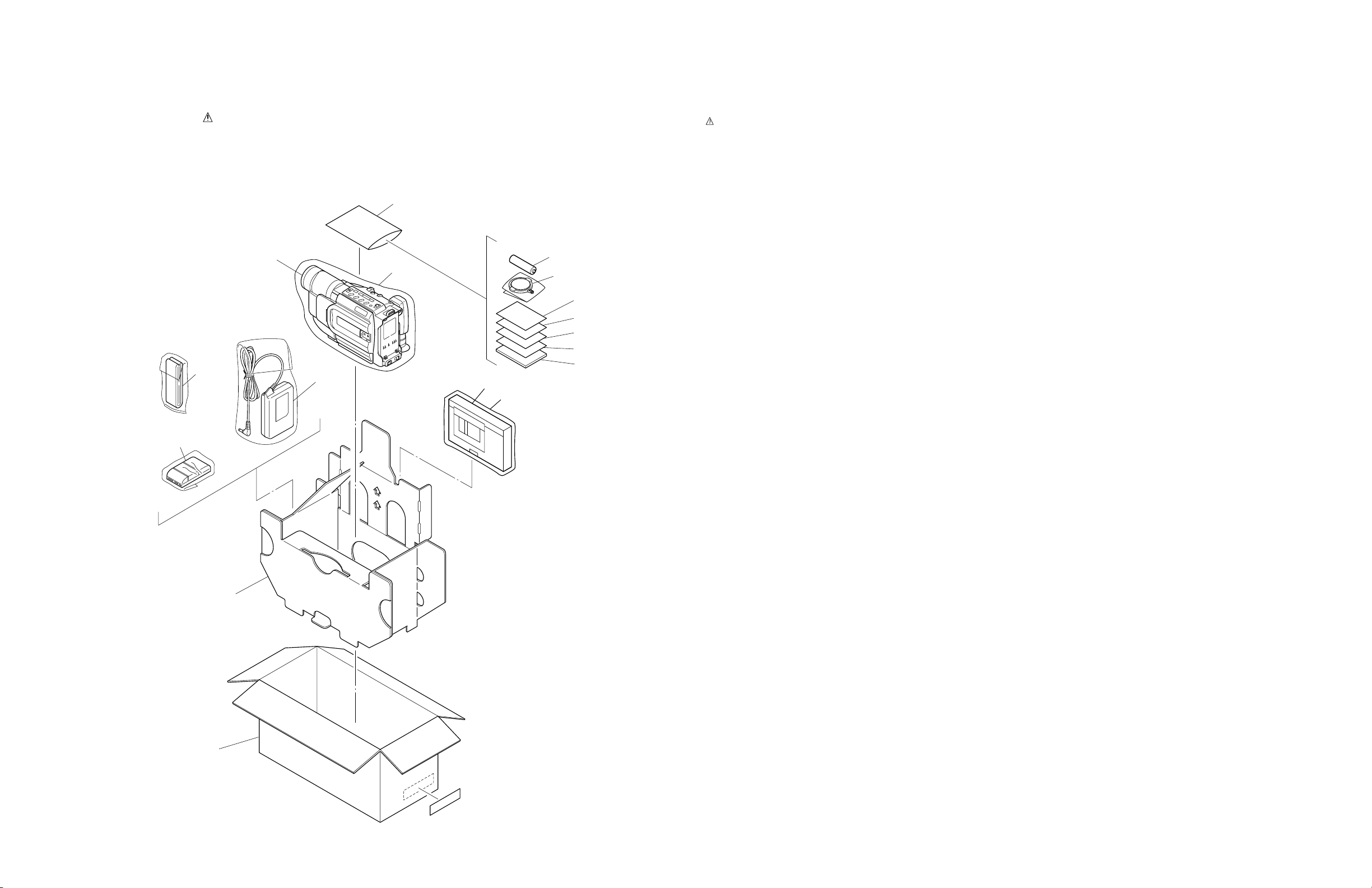
5.1 PACKING AND ACCESSORY ASSEMBLY <M1>
The instruction manual to be provided with this product will differ according to the destination.
4
FINAL ASSY
14
<M2>
11
3
21
22
16
15
9
8
7
6
5
# REF No. PART No. PART NAME, DESCRIPTION
---------------- ----------------------- -----------------------------------------------------
******************************
PACKING AND ACCESSORY ASSEMBLY <M1>
1 LY32179-001A PACKING CASE
2 LY32553-001A CUSHION
3 LY30023-002A POLY BAG
4 QPA02003506 POLY BAG
!
5 LYT0880-001C INST.BOOK(EN),AX970U
!
!
6 BT-51028-1 REGIST.CARD,AX970U
7 BT-51005-5 WARRANTY INF.,AX970U
8 BT-52004-2 WARRANTY CARD,AX770UC
9 BT-20071B SER.NET CARD,AX770UC
!
11 LY20848-001B AC ADAPTER,AP-V12U
!
13 YQ10629A BATTERY PACK,BN-V11U
14 LY20186-001A SHOULDER STRAP
15 LY43388-001A LENS CAP ASSY
16 – BATTERY,AA(R6)
21 YQ31963B-3 CASSETTE ADAPTER,C-P7U
22 YQ43446 POLY BAG
LYT0921-001A INST.BOOK(EN),AX770UC
LYT0923-001A INST.BOOK(FR),AX770UC
13
• INSTRUCTIONS
EN ....... ENGLISH
FR ....... FRENCH
2
1
LABEL
(SERIAL)
5-1 5-2
Page 3
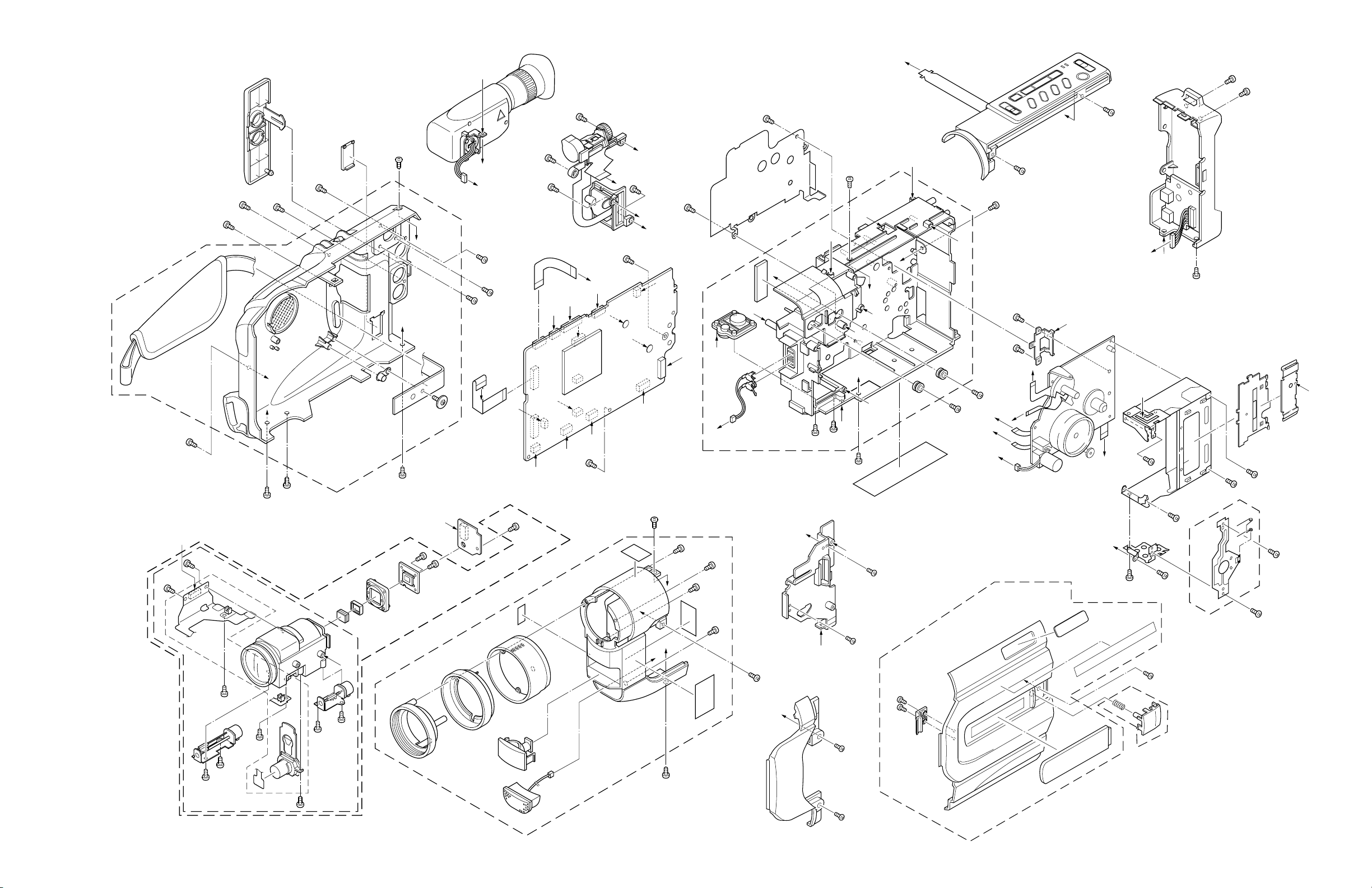
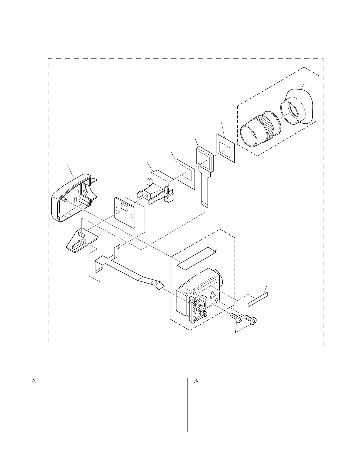
5.2 FINAL ASSEMBLY <M2>
111
117
117
110
110B
116
ss
251C
251C
251C
251B
251C
251C
251C
116
114
j
h
116
118
OPTICAL BLOCK
SECTION
251A
251C
251D
251C
252
253
251C
125
131
ELECTRONIC
gg
u
VIEWFINDER
112
115
<M4>
v
nn
148
148
148
147
ff
p
148
141
142
149
f
126
v
126
131
130
139
p
c
d
a
b
rr
140D
pp
m
140D
150
110A
s
144
n
MAIN
<01>
nn
140A
k
e
140C
j
u
146
113
113
g
113
bb
y
ff
z
s
gg
n
h
aa
140E
140E
140F
w
140B
140B
110C
145
ss
w
jj
cc
dd
ee
x
143
116
CCD
<02>
y
257
256
256
135
135H
255
254
135K
135C
251
e
135B
136
b
a
135E
k
135E
135E
135J
m
135E
jj
136
135A
mm
135F
135G
103
151
mm
105
107
105
rr
101E
104
101E
101D
RATING
LABEL
101
136
135D
104
149
f
aa
g
140
131
162
161
MECHANISM
<M3>
c
162
158
157
kk
150
dd
bb
z
155
d
ee
x
cc
pp
165
156
164
163
156
156
156
159
159A
160
160
101B
kk
101A
101C
106A
102
106
5-3 5-4
Page 4

# REF No. PART No. PART NAME, DESCRIPTION # REF No. PART No. PART NAME, DESCRIPTION
---------------- ----------------------- ----------------------------------------------------- ----------------- ----------------------- -----------------------------------------------------
147 LY20613-001B ZOOM UNIT
******************************
FINAL ASSEMBLY <M2>
101 LY20680-019A CASSETTE COVER(S)ASSY
101A LY32405-001A PLATE(WINDOW S)
101B LY42883-001A MARK
101C LY32562-003A STICKER(B)
101D LY32024-001B HINGE(CASSETTE COVER)
101E QYSLSF2060D SCREW,X2
102 QYSLSP2030D SCREW
103 LY10272-020A UPPER CASE(S),AX770UC
LY10272-026A UPPER CASE(S),AX970U
104 QYSLSF2060D SCREW,X2
105 QYSLSF2060D SCREW,X2
106 LY32041-001E BUTTON(PUSH)ASSY
106A LY30002-049B COMPRESSION SPRING
107 LY32038-001A UPPER COVER(S)ASSY
110 LY20684-001B LOWER CASE ASSY
110A LY40081-001A CAP
110B LY20682-001A GRIP BELT
110C LY30018-003A SPECIAL SCREW
111 LY31945-003A COVER(JACK)
112 LY31946-001A COVER(JIG)
113 QYSLSF2050Z SCREW,X3
114 QYSLSF2060D SCREW
115 QYSLSF2060D SCREW
116 QYSLSF2060D SCREW,X4
117 QYSLSF2060D SCREW,X2
118 QYSLSF2060D SCREW
125 LY20614-004C TOP OPE UNIT,AX770UC
LY20614-010C TOP OPE UNIT,AX970U
126 QYSLSF2060D SCREW,X2
130 LY20615-006E REAR UNIT
131 QYSLSF2060D SCREW,X3
135 LY20683-034A FRONT COVER ASSY,AX970U
LY20683-038A FRONT COVER ASSY,AX770UC
135A LY31937-001A HOOD
135B LY31938-001A COVER(HOOD)
135C LY31936-001A RING
135D LY32482-001A MICROPHONE
135E QYSLSF2060D SCREW,X4
135F LY30934-017A COVER(LIGHT),AX770UC
LY32040-001A DC LIGHT,AX970U
135G LY32058-001A STICKER(A),AX770UC
LY32058-002A STICKER(A),AX970U
135H LY32060-005A STICKER(C)
135J LY30029-0B4A SPACER(A),AX970U
!
135K YQ44341-6 CAUTION LABEL
136 QYSLSF2060D SCREW,X3
139 QYSPSTU1725M SCREW
140 LY20832-001B FRAME ASSY,AX970U
LY20832-002B FRAME ASSY,AX770UC
140A YQ31843 BASE
140B QYSLSF2060D SCREW,X2
140C LY30029-0A4A SPACER(A)
140D LY41082-001A CUSHION(OP),X2
140E YQ43810-1-1 CONTACT(LIGHT),X2,AX970U
140F WJM0259-001A E-SI C WIRE C-F,AX970U
141 LY32327-001A SHIELD CASE(MAIN)
142 QYSPSPU1720Z SCREW
143 QYSLSF2060D SCREW
144 QYSLSF2060D SCREW
145 WJT0072-001A E-CARD WIRE, OP-MAIN CN15
146 QAL0389-001 FPC, MAIN CN22-CCD CN5301
148 QYSLSF2060D SCREW,X4
149 LY41173-001A SPECIAL SCREW,X2
150 LY30018-050A SPECIAL SCREW,X2
151 QYSLSP2030D SCREW
155 LY31808-001C CASSETTE HOUSING FINAL ASSY
156 LY42722-003A SCREW,X4
157 LY31294-001B CASSETTE COVER INSIDE
158 LY32026-001B BRACKET(C.C/S)
159 LY31790-001A FRONT FRAME ASSY
159A YQ44144-1-1 TAPE GUIDE
160 SPSH1725M SCREW,X2
161 LY32326-001A BRACKET(MECHA)
162 LY42722-003A SCREW,X2
163 QYSLSF1750D SCREW
164 LY31807-001A SIDE BRACKET L
165 LY42722-003A SCREW
– OPTICAL BLOCK SECTION –
251 LY30948-003A OP BLOCK ASSY
251A PTY30948-002 FOCUS MOTOR
251B PTY30948-301 ZOOM MOTOR
251C PTY30151-016 TAPPING SCREW,X9
251D PTY30948-006 IRIS MOTOR UNIT
252 LY41757-001A OPTICAL LPF
253 LY31441-001A SPACER RUBBER
254 LY20346-001A CCD SPACER
255 LYH30374-001A CCD BASE ASSY
256 QYSPSGU2080Z SCREW,X2
257 LY30018-072A SPECIAL SCREW
5-5
Page 5
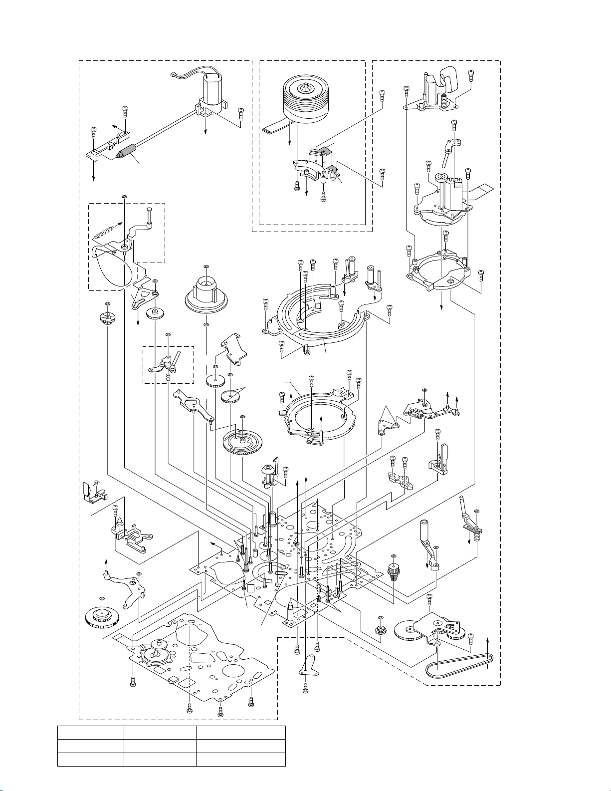
5.3 MECHANISM ASSEMBLY <M3>
400
410
410
j
409
AA
g
440
j
411
439A
404
414
405
AA
b
403
402
b
439
414
413
412
430
429A
428
461
429
BEWARE OF BOGUS PARTS
Parts that do not meet specifications may cause trouble in regard to safety
and performance. We recommend that genuine JVC parts be used.
457
420
419
469
458
459
426
n
423
427
401
470
442
457
455
445
445
441
434
433
465
c
470
m
425
AA
468
465
464
408
410
h
453
454
421
418
AA
417
416
415
BB
g
425
425
423
431
469B
AA
432
AA
x
425
n
425
423
x
y
h
425
AA
469A
AA
469B
425
425
424
AA
423
m
422
y
a
463
436
435
459
447
446
445
444
442
443
c
d
462
438
437
d
5-6
467
460
467
466
467
BB
AA
467
452
451
Classification Part No. Symbol in drawing
Grease KYODO-SH-P AA
Oil YTU94027 BB
450
457
449
456
471
BB
471
472
473
NOTE:The section marked in AA and BB indicate
lubrication and greasing areas.
450
448
a
Page 6

# REF No. PART No. PART NAME, DESCRIPTION # REF No. PART No. PART NAME, DESCRIPTION
---------------- ----------------------- ----------------------------------------------------- ----------------- ----------------------- -----------------------------------------------------
******************************
MECHANISM ASSEMBLY <M3>
400 YMA0033A-E MECHA(B)ASSY
401 LY20612-001B MAIN DECK ASSY
402 LY31817-001A CASSETTE GUIDE(LEFT)
403 LY31815-001A SW LEVER(LEFT)
404 LY42581-001A TORSION SPRING
405 LY42722-001A SCREW
408 LY31826-001A MOTOR BRACKET ASSY
409 YQ20793 WORM BRACKET
410 LY42722-001A SCREW,X3
411 LY31925-001A WHEEL GEAR
412 LY42730-001A MIDDLE GEAR
413 LY42521-001A CANCEL LEVER ASSY
414 LY42754-003A SLIT WASHER,X2
415 YQ20827-2-1 CONTROL CAM
416 PQM30017-25 SLIT WASHER
417 LY42733-001A LOADING GEAR(T)ASSY
418 LY42754-003A SLIT WASHER
419 LY42732-001A LOADING GEAR(S)ASSY
420 LY42754-003A SLIT WASHER
421 LY42403-001A COVER PLATE
422 LY42452-001A LOADING RING ASSY
423 LY42728-001A SCREW,X4
424 LY10239-001A GUIDE RAIL
425 LY42728-001A SCREW,X8
426 LY30161-001B POLE BASE(S)ASSY
427 LY30162-002A POLE BASE(T)ASSY
428 LY42523-001A DRIVE LEVER ASSY
429 LY42545-001A SLANT ARM ASSY
429A LY42547-001A TORSION SPRING(S)
430 LY42754-003A SLIT WASHER
431 LY42739-003A ROLLER BASE ASSY
432 LY42722-001A SCREW
433 LY42494-001A LINK ARM ASSY
434 PQM30017-25 SLIT WASHER
435 LY40018-002A PINCH ROLLER ARM ASSY
436 PQM30017-25 SLIT WASHER
437 LY42541-001B TAKE UP GUIDE ARM ASSY
438 LY42754-003A SLIT WASHER
439 LY42571-001A TENSION ARM ASSY
439A LY42669-001A TENSION SPRING
440 LY42754-003A SLIT WASHER
441 YQ20797-1-5 MOTOR BASE
442 LY42722-001A SCREW,X2
443 YQ44460 SCREW
444 QAR0212-001 CAPSTAN MOTOR
445 YQ44304 TAPPING SCREW,X3
446 LY42731-001A SLANT POLE BASE ASSY
447 YQ44304 TAPPING SCREW
448 YQ43710-2 TIMING BELT
449 LY42678-001A CENTER PULLEY UNIT
450 LY42722-002A SCREW,X2
451 LY42670-001A SUPPLY CLUTCH ASSY
452 LY42754-003A SLIT WASHER
453 YQ31861-1-7 REEL DISC
454 LY42755-001A WASHER
455 LY31924-001A TAKE UP GEAR
456 LY42738-001A BRAKE SUB GEAR
457 LY42754-003A SLIT WASHER,X3
458 LY42544-001B A/C HEAD UNIT
459 SPSN1750Z SCREW,X2
460 LY42517-001A EJECT LEVER ASSY
461 LY42754-003A SLIT WASHER
462 YQ31833-1-1 LED GUIDE
463 LY42722-001A SCREW
464 LY42729-001A DRUM SPACER
465 LY42722-001A SCREW,X2
466 QSW0888-001 ROTARY ENCODER
467 LY42722-002A SCREW,X4
468 LY31814-001A LINK LEVER
469 YDV2098A DRUM ASSY
469A YDM1003-1-5 CATCHER
469B QYSPSPU1735M SCREW,X2
470 LY42722-001A SCREW,X2
471 SPSH1740Z SCREW,X2
472 LY43542-001A BRUSH
473 LY42722-003A SCREW
5-7
Page 7
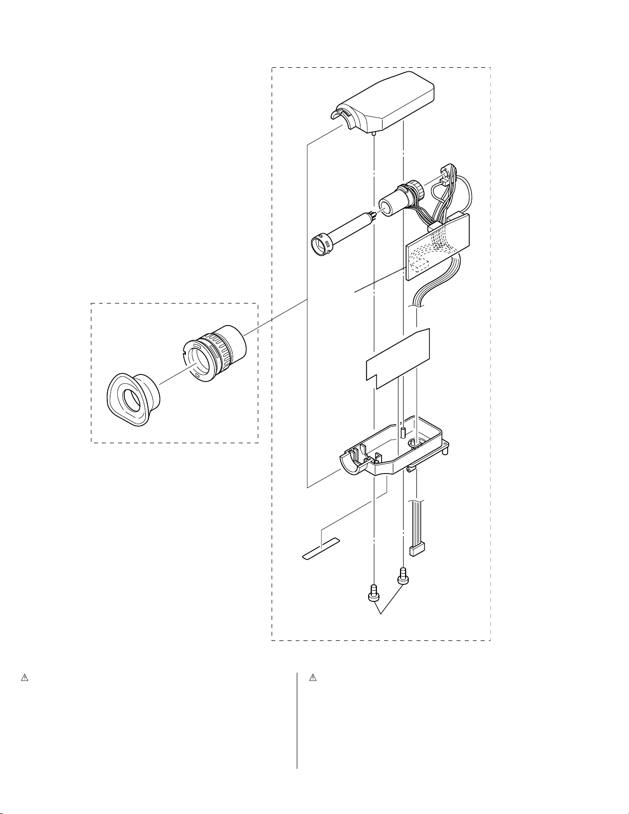
5.4 ELECTRONIC VIEWFINDER ASSEMBLY <M4> [GR-AX770UC]
350
353
352
351
357A
357
ELECTRONIC
VIEWFINDER
<60>
SERIAL NO.
LABEL
a
355
356
a
354
# REF No. PART No. PART NAME, DESCRIPTION # REF No. PART No. PART NAME, DESCRIPTION
--------------- ----------------------- ----------------------------------------------------- ---------------- ----------------------- ------------------------------------------------------
!
******************************
ELECTRONIC VIEWFINDER ASSEMBLY <M4>
!
350 LY20701-007A B/W VF ASSY
!
351 PEDP0193 CRT
!
352 QQD0026-001 DEFLECTION YOKE
5-8
353 LY10165-001B CASE(L)
354 QYSPSGU1760M TAP SCREW,X2
!
355 LY41280-001A SHEET(SHIELD)
!
356 PTY20701-011 BOTTOM CASE ASSY
357 PTY20374-201 LENS ASSY
357A LY20411-001A EYE CAP
Page 8
5.4 ELECTRONIC VIEWFINDER ASSEMBLY <M4> [GR-AX970U]
300
307
BL
<06>
302
303
304
301
309
309A
305
301A
C-VF
<06>
310
SERIAL NO.
LABEL
308
# REF No. PART No. PART NAME, DESCRIPTION # REF No. PART No. PART NAME, DESCRIPTION
--------------- ----------------------- ----------------------------------------------------- ---------------- ----------------------- ------------------------------------------------------
******************************
ELECTRONIC VIEWFINDER ASSEMBLY <M4>
!
300 LY20846-001A CVF ASSY
!
301 LY32068-001A BOTTOM CASE ASSY
301A LY42882-001A LABEL(COL/CAUT)
302 LY32321-001A HOLDER(LED)
303 LY43510-001A SPACER(HOLDER)
304 QLD0117-001 LCD MODULE
305 LY43418-001B SPACER(LED)
!
307 LY10137-001C TOP CASE
308 QYSPSGT1760D SCREW,X2
309 LY20309-001B EYE PIECE.ASSY
309A PTY20307-201 EYE CAP
310 QAL0397-001 FPC
5-9
Page 9

5.5 ELECTRICAL PARTS LIST
# REF No. PART No. PART NAME, DESCRIPTION # REF No. PART No. PART NAME, DESCRIPTION
---------------- ----------------------- ----------------------------------------------------- ----------------- ----------------------- -----------------------------------------------------
Q2023 2SC4617/QR/-X TRANSISTOR
******************************
MAIN BOARD ASSEMBLY <01>
PW1 YB10356UD1-01 MAIN BOARD ASSY,AX770UC
YB10356US1 MAIN BOARD ASSY,AX970U
IC101 UPD703039-040 EC(MICRO C ROM)
or UPD70F3040-040 IC(MICRO C ROM)
IC102 AT25080N-10SC-X IC
or CAT25C08SI IC
or X25170S8I-2.5-X IC
or 25LC080-I/SN-X IC
IC103 RS5C314 IC
IC104 IC-PST3427U-X IC
!
IC1601 LB11951WA-MPB IC
IC1602 TA75S393F IC
IC2001 MC74AC04DT IC
or TC74AC04FT IC(DIGITAL)
IC3501 HA118224F IC
IC4001 JCY0140-3 IC
IC4003 UPD6467GR-512-X IC(MICRO C ROM)
IC4201 BA10324AF-XE IC
IC4202 BA10324AF-XE IC
IC4501 UPD16835AGS IC
IC4701 MM1512XN IC
IC5201 HD49326BF IC
IC5202 JCY0098 IC
IC6001 FA7706F IC
IC6801 S-814A33AUC-W IC
IC7005 BA4558F IC,AX970U
Q101 2SA1774/RS/-X TRANSISTOR
or 2SA1836/6-7/-X TRANSISTOR
Q102 DTC144EE DIGI TRANSISTOR
or RN1104 DIGI TRANSISTOR
or UN9213J DIGI TRANSISTOR
Q103 2SC4617/QR/-X TRANSISTOR
or 2SC4783/5-6/-X TRANSISTOR
Q104 DTC144EE DIGI TRANSISTOR
or RN1104 DIGI TRANSISTOR
or UN9213J DIGI TRANSISTOR
Q105 2SA1774/RS/-X TRANSISTOR
or 2SA1836/6-7/-X TRANSISTOR
Q108 DTC114EE DIGI TRANSISTOR
or RN1102 DIGI TRANSISTOR
or UN9211J DIGI TRANSISTOR
Q109 DTC114EE DIGI TRANSISTOR
or RN1102 DIGI TRANSISTOR
or UN9211J DIGI TRANSISTOR
Q1601 2SC4617/QR/-X TRANSISTOR
or 2SC4783/5-6/-X TRANSISTOR
Q2001 DTA114TE DIGI TRANSISTOR
Q2007 PUMX1 PAIR TRANSISTOR
or UMX1N PAIR TRANSISTOR
or HN1C01FU/G/-X PAIR TRANSISTOR
Q2008 PUMT1 PAIR TRANSISTOR
or HN1A01FU/G/-X PAIR TRANSISTOR
or UMT1N PAIR TRANSISTOR
Q2021 DTC144EE DIGI TRANSISTOR
or RN1104 DIGI TRANSISTOR
or UN9213J DIGI TRANSISTOR
Q2022 DTC144EE DIGI TRANSISTOR
or RN1104 DIGI TRANSISTOR
or UN9213J DIGI TRANSISTOR
!
or 2SC4783/5-6/-X TRANSISTOR
Q2071 2SC4617/QR/-X TRANSISTOR
or 2SC4783/5-6/-X TRANSISTOR
Q3501 HN1C01FU/G/-X PAIR TRANSISTOR
Q3502 HN1C01FU/G/-X PAIR TRANSISTOR
Q3901 HN1A01FU/G/-X PAIR TRANSISTOR
Q4201 2SC4617/QR/-X TRANSISTOR
or 2SC4783/5-6/-X TRANSISTOR
Q4202 2SC4617/QR/-X TRANSISTOR
or 2SC4783/5-6/-X TRANSISTOR
Q4251 RPM-22PB PHOTO TRANSISTOR
Q4501 DTC114EE DIGI TRANSISTOR
or RN1102 DIGI TRANSISTOR
or UN9211J DIGI TRANSISTOR
Q4701 2SA1774/QR/-X TRANSISTOR
or 2SA1836/5-6/-X TRANSISTOR
Q4702 2SA1774/QR/-X TRANSISTOR
or 2SA1836/5-6/-X TRANSISTOR
Q6101 SSM5G01TU MOS FET
Q6201 SSM5G01TU MOS FET
Q6301 FDC6506P MOS FET
Q6306 SSM3K02F MOS FET,AX970U
Q6401 SSM5G01TU MOS FET
Q6501 SSM5G01TU MOS FET
Q6608 DTC144EE DIGI TRANSISTOR
or RN1104 DIGI TRANSISTOR
or UN9213J DIGI TRANSISTOR
Q6621 HN1C01FU/G/-X PAIR TRANSISTOR,AX970U
Q6622 2SA1577/QR/-X TRANSISTOR,AX970U
or 2SA1608/3-4/-X TRANSISTOR,AX970U
Q6701 TPC6102 MOS FET
Q6702 2SC4097/QR/-X TRANSISTOR
or 2SC4173/3-4/-X TRANSISTOR
Q6802 DTA113ZU DIGI TRANSISTOR
Q6811 2SA1577/QR/-X TRANSISTOR
or 2SA1608/3-4/-X TRANSISTOR
Q7001 PUMX1 PAIR TRANSISTOR,AX970U
or HN1C01FU/G/-X PAIR TRANSISTOR,AX970U
or UMX1N PAIR TRANSISTOR,AX970U
Q7003 PUMX1 PAIR TRANSISTOR,AX970U
or HN1C01FU/G/-X PAIR TRANSISTOR,AX970U
or UMX1N PAIR TRANSISTOR,AX970U
Q7005 PUMX1 PAIR TRANSISTOR,AX970U
or HN1C01FU/G/-X PAIR TRANSISTOR,AX970U
or UMX1N PAIR TRANSISTOR,AX970U
Q7301 2SA1774/QR/-X TRANSISTOR,AX770UC
or 2SA1836/5-6/-X TRANSISTOR,AX770UC
Q7303 UMD3N DIGI TRANSISTOR,AX970U
Q7304 PUMX1 PAIR TRANSISTOR,AX970U
or HN1C01FU/G/-X PAIR TRANSISTOR,AX970U
or UMX1N PAIR TRANSISTOR,AX970U
Q7310 CPH3101 TRANSISTOR,AX770UC
Q7311 2SC4617/QR/-X TRANSISTOR,AX770UC
or 2SC4783/5-6/-X TRANSISTOR,AX770UC
D101 SB007W03Q SB DIODE
D102 UDZS7.5B ZENER DIODE
D103 1SS355 DIODE
D104 1SS355 DIODE
D5201 1SS355 DIODE
D6301 MBR130 SB DIODE
D6601 RB480Y SB DIODE
D6602 RB480Y SB DIODE
5-10
Page 10

# REF No. PART No. PART NAME, DESCRIPTION # REF No. PART No. PART NAME, DESCRIPTION
---------------- ----------------------- ----------------------------------------------------- ----------------- ----------------------- -----------------------------------------------------
D6616 UDZS8.2B ZENER DIODE
D6701 CRS09 SB DIODE
D6702 CRS09 SB DIODE
R101 NRSA63J-104X MG RESISTOR 100kØ,1/16W
R102 NRSA63J-0R0X MG RESISTOR 0Ø,1/16W
R103 NRSA63J-0R0X MG RESISTOR 0Ø,1/16W
R105 NRSA63J-103X MG RESISTOR 10kØ,1/16W
R106 NRSA63J-102X MG RESISTOR 1kØ,1/16W
R107 NRVA63D-153X CMF RESISTOR 15kØ,1/16W
R108 NRVA63D-243X CMF RESISTOR 24kØ,1/16W
R109 NRVA63D-183X CMF RESISTOR 18kØ,1/16W
R110 NRSA63J-103X MG RESISTOR 10kØ,1/16W
R111 NRSA63J-273X MG RESISTOR 27kØ,1/16W
R112 NRSA63J-331X MG RESISTOR 330Ø,1/16W
R113 NRSA63J-562X MG RESISTOR 5.6kØ,1/16W
R114 NRSA63J-821X MG RESISTOR 820Ø,1/16W
R115 NRSA63J-101X MG RESISTOR 100Ø,1/16W
R117 NRSA63J-102X MG RESISTOR 1kØ,1/16W
R118 NRSA63J-103X MG RESISTOR 10kØ,1/16W
R119 NRSA63J-103X MG RESISTOR 10kØ,1/16W
R120 NRSA63J-273X MG RESISTOR 27kØ,1/16W
R121 NRSA63J-273X MG RESISTOR 27kØ,1/16W
R122 NRSA63J-393X MG RESISTOR 39kØ,1/16W
R125 NRSA63J-273X MG RESISTOR 27kØ,1/16W
R126 NRSA63J-153X MG RESISTOR 15kØ,1/16W
R127 NRSA63J-221X MG RESISTOR 220Ø,1/16W
R128 NRSA63J-102X MG RESISTOR 1kØ,1/16W
R129 NRSA63J-102X MG RESISTOR 1kØ,1/16W
R130 NRSA63J-105X MG RESISTOR 1MØ,1/16W
R136 NRSA63J-474X MG RESISTOR 470kØ,1/16W
R138 NRSA63J-333X MG RESISTOR 33kØ,1/16W
R139 NRSA63J-104X MG RESISTOR 100kØ,1/16W
R140 NRSA63J-753X MG RESISTOR 75kØ,1/16W
R141 NRSA63J-334X MG RESISTOR 330kØ,1/16W
R142 NRSA63J-103X MG RESISTOR 10kØ,1/16W
R143 NRSA63J-105X MG RESISTOR 1MØ,1/16W
R144 NRSA63J-221X MG RESISTOR 220Ø,1/16W
R145 NRSA63J-222X MG RESISTOR 2.2kØ,1/16W
R146 NRSA63J-222X MG RESISTOR 2.2kØ,1/16W
R147 NRSA63J-472X MG RESISTOR 4.7kØ,1/16W
R148 NRSA63J-222X MG RESISTOR 2.2kØ,1/16W
R149 NRSA63J-222X MG RESISTOR 2.2kØ,1/16W
R150 NRSA63J-222X MG RESISTOR 2.2kØ,1/16W
R151 NRSA63J-222X MG RESISTOR 2.2kØ,1/16W
R152 NRSA63J-474X MG RESISTOR 470kØ,1/16W
R153 NRSA63J-474X MG RESISTOR 470kØ,1/16W
R154 NRSA63J-222X MG RESISTOR 2.2kØ,1/16W
R155 NRSA63J-104X MG RESISTOR 100kØ,1/16W
!
R156 NRSA63J-102X MG RESISTOR 1kØ,1/16W
R157 NRSA63J-0R0X MG RESISTOR 0Ø,1/16W
R158 NRSA63J-222X MG RESISTOR 2.2kØ,1/16W
R159 NRSA63J-222X MG RESISTOR 2.2kØ,1/16W
R160 NRSA63J-104X MG RESISTOR 100kØ,1/16W
R162 NRSA63J-472X MG RESISTOR 4.7kØ,1/16W
R163 NRSA63J-103X MG RESISTOR 10kØ,1/16W
R164 NRSA63J-221X MG RESISTOR 220Ø,1/16W
R165 NRSA63J-151X MG RESISTOR 150Ø,1/16W
R166 NRSA63J-105X MG RESISTOR 1MØ,1/16W
R167 NRSA63J-183X MG RESISTOR 18kØ,1/16W
R168 NRSA63J-562X MG RESISTOR 5.6kØ,1/16W
R169 NRSA63J-331X MG RESISTOR 330Ø,1/16W
R170 NRSA63J-333X MG RESISTOR 33kØ,1/16W
R171 NRSA63J-222X MG RESISTOR 2.2kØ,1/16W
R172 NRSA63J-222X MG RESISTOR 2.2kØ,1/16W
R177 NRSA63J-183X MG RESISTOR 18kØ,1/16W
R178 NRSA63J-562X MG RESISTOR 5.6kØ,1/16W
R179 NRSA63J-331X MG RESISTOR 330Ø,1/16W
R180 NRSA63J-333X MG RESISTOR 33kØ,1/16W
R181 NRSA63J-0R0X MG RESISTOR 0Ø,1/16W
R183 NRSA63J-105X MG RESISTOR 1MØ,1/16W
R185 NRSA63J-0R0X MG RESISTOR 0Ø,1/16W
R188 NRSA63J-472X MG RESISTOR 4.7kØ,1/16W
R189 NRSA63J-331X MG RESISTOR 330Ø,1/16W
R190 NRSA63J-105X MG RESISTOR 1MØ,1/16W
R1601 NRV142F-R33X CMF RESISTOR 0.33Ø,1/4W
R1602 NRV142F-R33X CMF RESISTOR 0.33Ø,1/4W
R1603 NRSA63J-153X MG RESISTOR 15kØ,1/16W
R1604 NRSA63J-153X MG RESISTOR 15kØ,1/16W
R1605 NRSA63J-102X MG RESISTOR 1kØ,1/16W
R1606 NRSA63J-104X MG RESISTOR 100kØ,1/16W
R1607 NRSA63J-471X MG RESISTOR 470Ø,1/16W
R1608 NRSA63J-154X MG RESISTOR 150kØ,1/16W
R1609 NRSA63J-471X MG RESISTOR 470Ø,1/16W
R1610 NRSA63J-104X MG RESISTOR 100kØ,1/16W
R1611 NRSA63J-153X MG RESISTOR 15kØ,1/16W
R1612 NRSA63J-153X MG RESISTOR 15kØ,1/16W
R1613 NRSA63J-104X MG RESISTOR 100kØ,1/16W
R1615 NRSA63J-152X MG RESISTOR 1.5kØ,1/16W
R1616 NRSA63J-152X MG RESISTOR 1.5kØ,1/16W
R1617 NRSA63J-153X MG RESISTOR 15kØ,1/16W
R1618 NRSA63J-153X MG RESISTOR 15kØ,1/16W
R1619 NRSA63J-334X MG RESISTOR 330kØ,1/16W
R1620 NRSA63J-221X MG RESISTOR 220Ø,1/16W
R1621 NRSA63J-331X MG RESISTOR 330Ø,1/16W
R1622 NRSA63J-221X MG RESISTOR 220Ø,1/16W
R1623 NRSA63J-0R0X MG RESISTOR 0Ø,1/16W
R1624 NRSA63J-333X MG RESISTOR 33kØ,1/16W
R1625 NRSA63J-123X MG RESISTOR 12kØ,1/16W
R1626 NRSA63J-103X MG RESISTOR 10kØ,1/16W
R1627 NRSA63J-223X MG RESISTOR 22kØ,1/16W
R1628 NRSA63J-103X MG RESISTOR 10kØ,1/16W
R2001 NRSA63J-104X MG RESISTOR 100kØ,1/16W
R2002 NRSA63J-332X MG RESISTOR 3.3kØ,1/16W
R2003 NRSA63J-102X MG RESISTOR 1kØ,1/16W
R2004 NRSA63J-681X MG RESISTOR 680Ø,1/16W
R2005 NRSA63J-272X MG RESISTOR 2.7kØ,1/16W
R2006 NRSA63J-102X MG RESISTOR 1kØ,1/16W
R2011 NRSA63J-101X MG RESISTOR 100Ø,1/16W
R2012 NRSA63J-101X MG RESISTOR 100Ø,1/16W
R2021 NRSA63J-103X MG RESISTOR 10kØ,1/16W
R2022 NRSA63J-334X MG RESISTOR 330kØ,1/16W
R2023 NRSA63J-151X MG RESISTOR 150Ø,1/16W
R2024 NRSA63J-133X MG RESISTOR 13kØ,1/16W
R2025 NRSA63J-823X MG RESISTOR 82kØ,1/16W
R2027 NRSA63J-102X MG RESISTOR 1kØ,1/16W
R2028 NRSA63J-102X MG RESISTOR 1kØ,1/16W
R2030 NRSA63J-104X MG RESISTOR 100kØ,1/16W
R2031 NRSA63J-332X MG RESISTOR 3.3kØ,1/16W
R2051 NRSA63J-102X MG RESISTOR 1kØ,1/16W
R2071 NRSA63J-473X MG RESISTOR 47kØ,1/16W
R2072 NRSA63J-562X MG RESISTOR 5.6kØ,1/16W
R3501 NRSA63J-0R0X MG RESISTOR 0Ø,1/16W
R3502 NRSA63J-102X MG RESISTOR 1kØ,1/16W
R3506 NRSA63J-102X MG RESISTOR 1kØ,1/16W
R3507 NRSA63J-0R0X MG RESISTOR 0Ø,1/16W
R3508 NRSA63J-153X MG RESISTOR 15kØ,1/16W
5-11
Page 11

# REF No. PART No. PART NAME, DESCRIPTION # REF No. PART No. PART NAME, DESCRIPTION
---------------- ----------------------- ----------------------------------------------------- ----------------- ----------------------- -----------------------------------------------------
R3901 NRSA63J-100X MG RESISTOR 10Ø,1/16W
R3902 NRSA63J-101X MG RESISTOR 100Ø,1/16W
R3903 NRSA63J-182X MG RESISTOR 1.8kØ,1/16W
R4001 NRSA63J-102X MG RESISTOR 1kØ,1/16W
R4002 NRSA63J-105X MG RESISTOR 1MØ,1/16W
R4003 NRSA63J-563X MG RESISTOR 56kØ,1/16W
R4004 NRSA63D-153X MG RESISTOR 15kØ,1/16W
R4009 NRSA63D-153X MG RESISTOR 15kØ,1/16W
R4010 NRSA63D-153X MG RESISTOR,AX970U 15kØ,1/16W
R4016 NRSA63J-0R0X MG RESISTOR 0Ø,1/16W
R4019 NRSA63D-822X MG RESISTOR 8.2kØ,1/16W
R4020 NRSA63D-471X MG RESISTOR 470Ø,1/16W
R4021 NRSA63D-181X MG RESISTOR 180Ø,1/16W
R4022 NRSA63D-182X MG RESISTOR 1.8kØ,1/16W
R4025 NRSA63D-222X MG RESISTOR 2.2kØ,1/16W
R4026 NRSA63J-563X MG RESISTOR 56kØ,1/16W
R4027 NRSA63J-104X MG RESISTOR 100kØ,1/16W
R4028 NRSA63J-104X MG RESISTOR 100kØ,1/16W
R4031 NRSA63J-102X MG RESISTOR,AX970U 1kØ,1/16W
R4032 NRSA63J-0R0X MG RESISTOR 0Ø,1/16W
R4033 NRSA63J-392X MG RESISTOR 3.9kØ,1/16W
R4034 NRSA63J-332X MG RESISTOR 3.3kØ,1/16W
R4035 NRSA63J-332X MG RESISTOR 3.3kØ,1/16W
R4201 NRSA63J-103X MG RESISTOR 10kØ,1/16W
R4202 NRSA63J-0R0X MG RESISTOR 0Ø,1/16W
R4203 NRSA63J-223X MG RESISTOR 22kØ,1/16W
R4204 NRSA63J-331X MG RESISTOR 330Ø,1/16W
R4205 NRSA63J-105X MG RESISTOR 1MØ,1/16W
R4206 NRSA63J-103X MG RESISTOR 10kØ,1/16W
R4207 NRSA63J-104X MG RESISTOR 100kØ,1/16W
R4208 NRSA63J-472X MG RESISTOR 4.7kØ,1/16W
R4209 NRSA63J-104X MG RESISTOR 100kØ,1/16W
R4210 NRSA63J-105X MG RESISTOR 1MØ,1/16W
R4211 NRSA63J-243X MG RESISTOR 24kØ,1/16W
R4214 NRSA63J-472X MG RESISTOR 4.7kØ,1/16W
R4215 NRSA63J-683X MG RESISTOR 68kØ,1/16W
R4216 NRSA63J-103X MG RESISTOR 10kØ,1/16W
R4217 NRSA63J-102X MG RESISTOR 1kØ,1/16W
R4218 NRSA63J-102X MG RESISTOR 1kØ,1/16W
R4219 NRSA63J-104X MG RESISTOR 100kØ,1/16W
R4220 NRSA63J-152X MG RESISTOR 1.5kØ,1/16W
R4221 NRSA63J-334X MG RESISTOR 330kØ,1/16W
R4222 NRSA63J-154X MG RESISTOR 150kØ,1/16W
R4223 NRSA63J-333X MG RESISTOR 33kØ,1/16W
R4224 NRSA63J-223X MG RESISTOR 22kØ,1/16W
R4251 NRSA63J-182X MG RESISTOR 1.8kØ,1/16W
R4252 NRSA63J-103X MG RESISTOR 10kØ,1/16W
R4253 NRSA63J-103X MG RESISTOR 10kØ,1/16W
R4254 NRSA63J-684X MG RESISTOR 680kØ,1/16W
R4255 NRSA63J-222X MG RESISTOR 2.2kØ,1/16W
R4256 NRSA63J-824X MG RESISTOR 820kØ,1/16W
R4257 NRSA63J-822X MG RESISTOR 8.2kØ,1/16W
R4258 NRSA63J-104X MG RESISTOR 100kØ,1/16W
R4259 NRSA63J-683X MG RESISTOR 68kØ,1/16W
R4262 NRSA63J-302X MG RESISTOR 3kØ,1/16W
!
R4501 NRSA63J-6R8X MG RESISTOR 6.8Ø,1/16W
!
R4502 NRSA63J-6R8X MG RESISTOR 6.8Ø,1/16W
!
R4503 NRSA63J-6R8X MG RESISTOR 6.8Ø,1/16W
!
R4504 NRSA63J-6R8X MG RESISTOR 6.8Ø,1/16W
R4505 NRSA63J-271X MG RESISTOR 270Ø,1/16W
R4507 NRSA63J-103X MG RESISTOR 10kØ,1/16W
R4508 NRSA63J-103X MG RESISTOR 10kØ,1/16W
R4512 NRSA63J-0R0X MG RESISTOR 0Ø,1/16W
R4514 NRSA63J-223X MG RESISTOR 22kØ,1/16W
R4515 NRSA63J-182X MG RESISTOR 1.8kØ,1/16W
R4701 NRSA63D-112X MG RESISTOR 1.1kØ,1/16W
R4703 NRSA63J-681X MG RESISTOR 680Ø,1/16W
R4704 NRSA63J-122X MG RESISTOR 1.2kØ,1/16W
R4706 NRSA63D-680X MG RESISTOR 68Ø,1/16W
R4707 NRSA63D-751X MG RESISTOR 750Ø,1/16W
R4709 NRSA63J-681X MG RESISTOR 680Ø,1/16W
R4710 NRSA63J-122X MG RESISTOR 1.2kØ,1/16W
R5201 NRSA63J-243X MG RESISTOR 24kØ,1/16W
R5202 NRSA63J-220X MG RESISTOR 22Ø,1/16W
R5213 NRSA63J-101X MG RESISTOR 100Ø,1/16W
R5214 NRSA63J-101X MG RESISTOR 100Ø,1/16W
R5215 NRSA63J-104X MG RESISTOR 100kØ,1/16W
R5216 NRSA63J-100X MG RESISTOR 10Ø,1/16W
R5217 NRSA63J-104X MG RESISTOR 100kØ,1/16W
R6001 NRSA63J-104X MG RESISTOR 100kØ,1/16W
R6002 NRSA63J-333X MG RESISTOR 33kØ,1/16W
R6003 NRVA63D-912X CMF RESISTOR 9.1kØ,1/16W
R6004 NRVA63D-681X CMF RESISTOR 680Ø,1/16W
R6005 NRVA63D-203X CMF RESISTOR 20kØ,1/16W
R6008 NRVA63D-103X CMF RESISTOR 10kØ,1/16W
R6012 NRSA63J-103X MG RESISTOR 10kØ,1/16W
R6015 NRSA63J-104X MG RESISTOR 100kØ,1/16W
R6021 NRSA63J-222X MG RESISTOR 2.2kØ,1/16W
R6024 NRSA63J-224X MG RESISTOR 220kØ,1/16W
R6025 NRSA63J-104X MG RESISTOR 100kØ,1/16W
R6026 NRSA63J-104X MG RESISTOR 100kØ,1/16W
R6027 NRSA63J-104X MG RESISTOR 100kØ,1/16W
R6028 NRSA63J-104X MG RESISTOR 100kØ,1/16W
R6029 NRSA63J-104X MG RESISTOR 100kØ,1/16W
R6103 NRVA63D-223X CMF RESISTOR 22kØ,1/16W
R6104 NRVA63D-103X CMF RESISTOR 10kØ,1/16W
R6203 NRVA63D-103X CMF RESISTOR 10kØ,1/16W
R6204 NRVA63D-123X CMF RESISTOR 12kØ,1/16W
R6303 NRVA63D-183X CMF RESISTOR 18kØ,1/16W
R6304 NRVA63D-472X CMF RESISTOR 4.7kØ,1/16W
R6306 NRS12BK-R47W MG RESISTOR,AX970U 0.47Ø,1/2W
R6307 NRSA63J-104X MG RESISTOR,AX970U 100kØ,1/16W
R6401 NRSA63J-0R0X MG RESISTOR 0Ø,1/16W
R6501 NRSA63J-0R0X MG RESISTOR 0Ø,1/16W
R6502 NRSA63J-471X MG RESISTOR 470Ø,1/16W
R6603 NRVA63D-683X CMF RESISTOR 68kØ,1/16W
R6604 NRVA63D-392X CMF RESISTOR 3.9kØ,1/16W
R6605 NRSA63J-274X MG RESISTOR 270kØ,1/16W
R6606 NRSA63J-272X MG RESISTOR 2.7kØ,1/16W
R6612 NRSA63J-823X MG RESISTOR 82kØ,1/16W
R6613 NRSA63J-104X MG RESISTOR 100kØ,1/16W
R6614 NRSA63J-153X MG RESISTOR 15kØ,1/16W
R6616 NRSA63J-102X MG RESISTOR 1kØ,1/16W
R6622 NRVA63D-104X CMF RESISTOR,AX970U 100kØ,1/16W
R6623 NRVA63D-473X CMF RESISTOR,AX970U 47kØ,1/16W
R6624 NRSA63J-273X MG RESISTOR,AX970U 27kØ,1/16W
R6625 NRSA63J-822X MG RESISTOR,AX970U 8.2kØ,1/16W
R6626 NRVA63D-273X CMF RESISTOR,AX970U 27kØ,1/16W
R6627 NRVA63D-183X CMF RESISTOR,AX970U 18kØ,1/16W
R6702 NRSA63J-330X MG RESISTOR 33Ø,1/16W
R6704 NRVA63D-123X CMF RESISTOR 12kØ,1/16W
R6706 NRZ0058-R20X MG RESISTOR 0.2Ø,1/2W
R6707 NRS016J-121X MG RESISTOR 120Ø,1W
R6708 NRS016J-121X MG RESISTOR 120Ø,1W
R6709 NRS016J-121X MG RESISTOR 120Ø,1W
R6710 NRVA63D-823X CMF RESISTOR 82kØ,1/16W
5-12
Page 12

# REF No. PART No. PART NAME, DESCRIPTION # REF No. PART No. PART NAME, DESCRIPTION
---------------- ----------------------- ----------------------------------------------------- ----------------- ----------------------- -----------------------------------------------------
R6711 NRVA63D-333X CMF RESISTOR 33kØ,1/16W
R6713 NRSA63J-562X MG RESISTOR 5.6kØ,1/16W
R6715 NRSA63J-222X MG RESISTOR 2.2kØ,1/16W
R6801 NRSA63J-0R0X MG RESISTOR 0Ø,1/16W
R6802 NRSA63J-104X MG RESISTOR 100kØ,1/16W
R6811 NRSA63J-101X MG RESISTOR 100Ø,1/16W
R6812 NRSA63J-222X MG RESISTOR 2.2kØ,1/16W
R6961 NRSA63J-223X MG RESISTOR 22kØ,1/16W
R7061 NRVA63D-183X CMF RESISTOR,AX970U 18kØ,1/16W
R7062 NRVA63D-334X CMF RESISTOR,AX970U 330kØ,1/16W
R7077 NRVA63D-123X CMF RESISTOR,AX970U 12kØ,1/16W
R7083 NRSA63J-105X MG RESISTOR,AX970U 1MØ,1/16W
R7085 NRVA63D-822X CMF RESISTOR,AX970U 8.2kØ,1/16W
R7086 NRVA63D-123X CMF RESISTOR,AX970U 12kØ,1/16W
R7088 NRVA63D-223X CMF RESISTOR,AX970U 22kØ,1/16W
R7090 NRVA63D-822X CMF RESISTOR,AX970U 8.2kØ,1/16W
R7091 NRVA63D-123X CMF RESISTOR,AX970U 12kØ,1/16W
R7093 NRVA63D-223X CMF RESISTOR,AX970U 22kØ,1/16W
R7095 NRVA63D-822X CMF RESISTOR,AX970U 8.2kØ,1/16W
R7096 NRVA63D-123X CMF RESISTOR,AX970U 12kØ,1/16W
R7098 NRVA63D-223X CMF RESISTOR,AX970U 22kØ,1/16W
R7099 NRVA63D-103X CMF RESISTOR,AX970U 10kØ,1/16W
R7100 NRVA63D-103X CMF RESISTOR,AX970U 10kØ,1/16W
R7101 NRVA63D-103X CMF RESISTOR,AX970U 10kØ,1/16W
R7102 NRVA63D-103X CMF RESISTOR,AX970U 10kØ,1/16W
R7103 NRVA63D-103X CMF RESISTOR,AX970U 10kØ,1/16W
R7123 NRSA63J-0R0X MG RESISTOR,AX970U 0Ø,1/16W
R7124 NRVA63D-103X CMF RESISTOR,AX970U 10kØ,1/16W
R7301 NRVA63D-182X CMF RESISTOR,AX770UC 1.8kØ,1/16W
R7305 NRVA63D-821X CMF RESISTOR,AX770UC 820Ø,1/16W
R7317 NRVA63D-332X CMF RESISTOR,AX970U 3.3kØ,1/16W
R7318 NRVA63D-561X CMF RESISTOR,AX970U 560Ø,1/16W
R7319 NRSA63J-360X MG RESISTOR,AX970U 36Ø,1/16W
R7321 NRSA63J-333X MG RESISTOR,AX970U 33kØ,1/16W
R7331 NRSA63J-103X MG RESISTOR,AX770UC 10kØ,1/16W
R7332 NRSA63J-152X MG RESISTOR,AX770UC 1.5kØ,1/16W
R7333 NRSA63J-473X MG RESISTOR,AX770UC 47kØ,1/16W
R7337 NRSA63J-0R0X MG RESISTOR,AX970U 0Ø,1/16W
R7338 NRSA63J-0R0X MG RESISTOR,AX970U 0Ø,1/16W
R7339 NRSA63J-0R0X MG RESISTOR,AX970U 0Ø,1/16W
RA101 NRZ0038-222X NETWORK RESISTOR 2.2kØ
RA102 NRZ0038-222X NETWORK RESISTOR 2.2kØ
RA103 NRZ0038-222X NETWORK RESISTOR 2.2kØ
RA104 NRZ0038-222X NETWORK RESISTOR 2.2kØ
RA106 NRZ0038-101X NETWORK RESISTOR 100Ø
RA107 NRZ0038-222X NETWORK RESISTOR 2.2kØ
RA108 NRZ0038-222X NETWORK RESISTOR 2.2kØ
RA109 NRZ0038-474X NETWORK RESISTOR 470kØ
RA110 NRZ0038-474X NETWORK RESISTOR 470kØ
RA111 NRZ0038-474X NETWORK RESISTOR 470kØ
RA112 NRZ0038-104X NETWORK RESISTOR 100kØ
RA6020 NRZ0038-102X NETWORK RESISTOR 1kØ
C103 NBE20JM-106X T CAPACITOR 10µF,6.3V
C104 NCB31EK-103X CAPACITOR 0.01µF,25V
C105 NCB21CK-224X CAPACITOR 0.22µF,16V
C107 NCB31EK-103X CAPACITOR 0.01µF,25V
C108 NBE21AM-225X T CAPACITOR 2.2µF,10V
C109 NBE20JM-106X T CAPACITOR 10µF,6.3V
C110 NDC31HJ-101X CAPACITOR 100pF,50V
C112 NEA70JM-226X E CAPACITOR 22µF,6.3V
C113 NCB31EK-103X CAPACITOR 0.01µF,25V
C114 NCB31EK-103X CAPACITOR 0.01µF,25V
C115 NCF31EZ-104X CAPACITOR 0.1µF,25V
C116 NCB31EK-103X CAPACITOR 0.01µF,25V
C118 NCF31EZ-104X CAPACITOR 0.1µF,25V
C119 NCB31EK-103X CAPACITOR 0.01µF,25V
C120 NCB31EK-103X CAPACITOR 0.01µF,25V
C121 NCF31EZ-104X CAPACITOR 0.1µF,25V
C122 NCF31EZ-104X CAPACITOR 0.1µF,25V
C123 NDC31HJ-100X CAPACITOR 10pF,50V
C124 NDC31HJ-100X CAPACITOR 10pF,50V
C125 NCB31EK-103X CAPACITOR 0.01µF,25V
C126 NDC31HJ-100X CAPACITOR 10pF,50V
C127 NCB31CK-333X CAPACITOR 0.033µF,16V
C128 NCB21CK-474X CAPACITOR 0.47µF,16V
C129 NCB31CK-333X CAPACITOR 0.033µF,16V
C131 NCF31EZ-104X CAPACITOR 0.1µF,25V
C132 NCF31EZ-104X CAPACITOR 0.1µF,25V
C133 NCF31EZ-104X CAPACITOR 0.1µF,25V
C134 NCF31EZ-104X CAPACITOR 0.1µF,25V
C138 NCB31EK-103X CAPACITOR 0.01µF,25V
C140 NDC31HJ-220X CAPACITOR 22pF,50V
C142 NCB31CK-104X CAPACITOR 0.1µF,16V
C143 NDC31HJ-3R0X CAPACITOR 3pF,50V
C144 NDC31HJ-101X CAPACITOR 100pF,50V
C1201 NCB31HK-102X CAPACITOR 0.001µF,50V
C1202 NBE20JM-106X T CAPACITOR 10µF,6.3V
C1205 NCB31EK-153X CAPACITOR 0.015µF,25V
C1206 NBE20JM-106X T CAPACITOR 10µF,6.3V
C1601 NCB21EK-104X CAPACITOR 0.1µF,25V
C1602 NCB30JK-105X CAPACITOR 1µF,6.3V
C1603 NCB31HK-472X CAPACITOR 0.0047µF,50V
C1604 NCB31HK-472X CAPACITOR 0.0047µF,50V
C1605 NCB31CK-333X CAPACITOR 0.033µF,16V
C1606 NCB21EK-104X CAPACITOR 0.1µF,25V
C1607 NCB21CK-474X CAPACITOR 0.47µF,16V
C1608 NCB31HK-332X CAPACITOR 0.0033µF,50V
C1609 NBE20JM-106X T CAPACITOR 10µF,6.3V
C1610 NCB31HK-681X CAPACITOR 680pF,50V
C1611 NCB31CK-104X CAPACITOR 0.1µF,16V
C1612 NCB21CK-105X CAPACITOR 1µF,16V
C1613 NCB31CK-333X CAPACITOR 0.033µF,16V
C1614 NCB31CK-104X CAPACITOR 0.1µF,16V
C1615 NCB31CK-104X CAPACITOR 0.1µF,16V
C1616 NCB31CK-104X CAPACITOR 0.1µF,16V
C1617 NCB31CK-104X CAPACITOR 0.1µF,16V
C1618 NCB31CK-104X CAPACITOR 0.1µF,16V
C1619 NCB31CK-104X CAPACITOR 0.1µF,16V
C1620 NBE21AM-106X T CAPACITOR 10µF,10V
C1621 NBP41CM-106X T CAPACITOR 10µF,16V
C1625 NCB31CK-104X CAPACITOR 0.1µF,16V
C1628 NDC31HJ-101X CAPACITOR 100pF,50V
C1630 NBE20JM-106X T CAPACITOR 10µF,6.3V
C2001 NBE20JM-106X T CAPACITOR 10µF,6.3V
C2002 NFV41HJ-183X MPPS CAPACITOR 0.018µF,50V
C2003 NDC31HJ-331X CAPACITOR 330pF,50V
C2004 NBE20JM-226X T CAPACITOR 22µF,6.3V
C2005 NCB21CK-105X CAPACITOR 1µF,16V
C2021 NCB31HK-682X CAPACITOR 0.0068µF,50V
C2022 NBE20JM-106X T CAPACITOR 10µF,6.3V
C2023 NBP21CM-105X T CAPACITOR 1µF,16V
C2024 NCB31HK-122X CAPACITOR 0.0012µF,50V
C2025 NCB21CK-105X CAPACITOR 1µF,16V
C2026 NCB31HK-222X CAPACITOR 0.0022µF,50V
C2027 NCB21CK-474X CAPACITOR 0.47µF,16V
C2028 NCB21CK-105X CAPACITOR 1µF,16V
5-13
Page 13

# REF No. PART No. PART NAME, DESCRIPTION # REF No. PART No. PART NAME, DESCRIPTION
---------------- ----------------------- ----------------------------------------------------- ----------------- ----------------------- -----------------------------------------------------
C2029 NCB21CK-105X CAPACITOR 1µF,16V
C2031 NCB31CK-104X CAPACITOR 0.1µF,16V
C2032 NCB31HK-472X CAPACITOR 0.0047µF,50V
C2033 NBE20JM-475X T CAPACITOR 4.7µF,6.3V
C2034 NCB31CK-104X CAPACITOR 0.1µF,16V
C2035 NBE20JM-226X T CAPACITOR 22µF,6.3V
C2036 NBE20JM-106X T CAPACITOR 10µF,6.3V
C2038 NCB21CK-474X CAPACITOR 0.47µF,16V
C2051 NCB31EK-103X CAPACITOR 0.01µF,25V
C2071 NBE20JM-106X T CAPACITOR 10µF,6.3V
C2072 NCB31HK-222X CAPACITOR 0.0022µF,50V
C3506 NCB31EK-103X CAPACITOR 0.01µF,25V
C3507 NCB31EK-103X CAPACITOR 0.01µF,25V
C3508 NCB31EK-103X CAPACITOR 0.01µF,25V
C3510 NCB31CK-104X CAPACITOR 0.1µF,16V
C3512 NCB10JK-106X CAPACITOR 10µF,6.3V
C3513 NCB31CK-223X CAPACITOR 0.022µF,16V
C3514 NCB30JK-105X CAPACITOR 1µF,6.3V
C3515 NCB31EK-103X CAPACITOR 0.01µF,25V
C3902 NCB31EK-103X CAPACITOR 0.01µF,25V
C3903 NDC31HJ-3R0X CAPACITOR 3pF,50V
C4002 NCF31EZ-104X CAPACITOR 0.1µF,25V
C4003 NCF31EZ-104X CAPACITOR 0.1µF,25V
C4004 NCF31EZ-104X CAPACITOR 0.1µF,25V
C4005 NCF31EZ-104X CAPACITOR 0.1µF,25V
C4006 NDC31HJ-100X CAPACITOR 10pF,50V
C4007 NCF31EZ-104X CAPACITOR 0.1µF,25V
C4008 NCF31EZ-104X CAPACITOR 0.1µF,25V
C4009 NDC31HG-100X CAPACITOR 10pF,50V
C4010 NDC31HG-100X CAPACITOR 10pF,50V
C4012 NCF31EZ-104X CAPACITOR 0.1µF,25V
C4013 NCF31EZ-104X CAPACITOR 0.1µF,25V
C4014 NCB31CK-104X CAPACITOR 0.1µF,16V
C4015 NCF31EZ-104X CAPACITOR 0.1µF,25V
C4016 NCB31CK-104X CAPACITOR 0.1µF,16V
C4017 NCF31EZ-104X CAPACITOR 0.1µF,25V
C4018 NCF31EZ-104X CAPACITOR 0.1µF,25V
C4019 NCF31EZ-104X CAPACITOR,AX970U 0.1µF,25V
C4020 NCB31CK-104X CAPACITOR,AX970U 0.1µF,16V
C4021 NCF31EZ-104X CAPACITOR 0.1µF,25V
C4023 NCF31EZ-104X CAPACITOR 0.1µF,25V
C4026 NCB10JK-106X CAPACITOR 10µF,6.3V
C4027 NCF31EZ-104X CAPACITOR 0.1µF,25V
C4028 NCF31EZ-104X CAPACITOR 0.1µF,25V
C4029 NCB31CK-104X CAPACITOR 0.1µF,16V
C4030 NCF31EZ-104X CAPACITOR 0.1µF,25V
C4031 NCB30JK-105X CAPACITOR 1µF,6.3V
C4032 NCF31EZ-104X CAPACITOR 0.1µF,25V
C4033 NCF31EZ-104X CAPACITOR 0.1µF,25V
C4034 NCF31EZ-104X CAPACITOR 0.1µF,25V
C4035 NCF31EZ-104X CAPACITOR 0.1µF,25V
C4036 NCF31EZ-104X CAPACITOR 0.1µF,25V
C4037 NCF31EZ-104X CAPACITOR 0.1µF,25V
C4038 NCF31EZ-104X CAPACITOR 0.1µF,25V
C4039 NCF31EZ-104X CAPACITOR 0.1µF,25V
C4042 NCB30JK-105X CAPACITOR,AX970U 1µF,6.3V
C4045 NCB30JK-105X CAPACITOR 1µF,6.3V
C4046 NDC31HJ-221X CAPACITOR 220pF,50V
C4047 NCF31EZ-104X CAPACITOR 0.1µF,25V
C4048 NCF31EZ-104X CAPACITOR 0.1µF,25V
C4201 NEA71HM-225X E CAPACITOR 2.2µF,50V
C4202 NCF31EZ-104X CAPACITOR 0.1µF,25V
C4203 NCB31CK-104X CAPACITOR 0.1µF,16V
C4205 NCB31EK-103X CAPACITOR 0.01µF,25V
C4206 NCB31CK-104X CAPACITOR 0.1µF,16V
C4207 NCB31EK-103X CAPACITOR 0.01µF,25V
C4208 NCB31CK-104X CAPACITOR 0.1µF,16V
C4209 NCB31CK-104X CAPACITOR 0.1µF,16V
C4210 NCF21CZ-105X CAPACITOR 1µF,16V
C4251 NEA71HM-335X E CAPACITOR 3.3µF,50V
C4252 NCB31CK-104X CAPACITOR 0.1µF,16V
C4253 NCB31EK-153X CAPACITOR 0.015µF,25V
C4254 NCB31EK-153X CAPACITOR 0.015µF,25V
C4256 NEA71CM-106X E CAPACITOR 10µF,16V
C4504 NCF31EZ-104X CAPACITOR 0.1µF,25V
C4505 NDC31HJ-330X CAPACITOR 33pF,50V
C4506 NCB31HK-102X CAPACITOR 0.001µF,50V
C4507 NCB31HK-102X CAPACITOR 0.001µF,50V
C4508 NCB31HK-102X CAPACITOR 0.001µF,50V
C4509 NCB31HK-102X CAPACITOR 0.001µF,50V
C4510 NCB31CK-104X CAPACITOR 0.1µF,16V
C4511 NCF31EZ-104X CAPACITOR 0.1µF,25V
C4512 NEA71CM-107X E CAPACITOR 100µF,16V
C4702 NDC31HJ-270X CAPACITOR 27pF,50V
C4703 NDC31HJ-150X CAPACITOR 15pF,50V
C4704 NCB30JK-105X CAPACITOR 1µF,6.3V
C4705 NCB31EK-103X CAPACITOR 0.01µF,25V
C4706 NEA70GM-107X E CAPACITOR 100µF,4.0V
C4707 NEA70JM-226X E CAPACITOR 22µF,6.3V
C4708 NCF31EZ-104X CAPACITOR 0.1µF,25V
C4709 NBE20JM-106X T CAPACITOR 10µF,6.3V
C4716 NDC31HJ-270X CAPACITOR 27pF,50V
C4717 NDC31HJ-150X CAPACITOR 15pF,50V
C5203 NCB10JK-106X CAPACITOR 10µF,6.3V
C5207 NCB31EK-103X CAPACITOR 0.01µF,25V
C5208 NCB31EK-103X CAPACITOR 0.01µF,25V
C5209 NCB31EK-103X CAPACITOR 0.01µF,25V
C5210 NCF31EZ-104X CAPACITOR 0.1µF,25V
C5211 NCB21CK-105X CAPACITOR 1µF,16V
C5212 NCB21CK-105X CAPACITOR 1µF,16V
C5213 NCB31HK-332X CAPACITOR 0.0033µF,50V
C5214 NCB31EK-103X CAPACITOR 0.01µF,25V
C5218 NCF31EZ-104X CAPACITOR 0.1µF,25V
C5219 NBP21CM-685X T CAPACITOR 6.8µF,16V
C5221 NCB11EK-105X CAPACITOR 1µF,25V
C5222 NCB31CK-104X CAPACITOR 0.1µF,16V
C5223 NCF31EZ-104X CAPACITOR 0.1µF,25V
C5225 NCF31EZ-104X CAPACITOR 0.1µF,25V
C5227 NCB31CK-104X CAPACITOR 0.1µF,16V
C5228 NCF31EZ-104X CAPACITOR 0.1µF,25V
C5229 NCB11EK-105X CAPACITOR 1µF,25V
C5230 NCB21EK-104X CAPACITOR 0.1µF,25V
C5232 NDC31HJ-100X CAPACITOR 10pF,50V
C5233 NDC31HJ-100X CAPACITOR 10pF,50V
C5234 NDC31HJ-100X CAPACITOR 10pF,50V
C5235 NDC31HJ-100X CAPACITOR 10pF,50V
C5236 NDC31HJ-100X CAPACITOR 10pF,50V
C5237 NDC31HJ-100X CAPACITOR 10pF,50V
C6002 NEA71CM-106X E CAPACITOR 10µF,16V
C6004 NCF21CZ-105X CAPACITOR 1µF,16V
C6005 NCB21CK-105X CAPACITOR 1µF,16V
C6006 NCB31EK-103X CAPACITOR 0.01µF,25V
C6007 NCB21CK-105X CAPACITOR 1µF,16V
C6009 NDC31HJ-101X CAPACITOR 100pF,50V
C6010 NCB21CK-224X CAPACITOR 0.22µF,16V
C6011 NCB31EK-103X CAPACITOR 0.01µF,25V
5-14
Page 14

# REF No. PART No. PART NAME, DESCRIPTION # REF No. PART No. PART NAME, DESCRIPTION
---------------- ----------------------- ----------------------------------------------------- ----------------- ----------------------- -----------------------------------------------------
C6012 NCB21CK-224X CAPACITOR 0.22µF,16V
C6013 NCB21CK-154X CAPACITOR 0.15µF,16V
C6014 NCB31CK-104X CAPACITOR 0.1µF,16V
C6015 NCB31CK-104X CAPACITOR 0.1µF,16V
C6016 NCB31EK-473X CAPACITOR 0.047µF,25V
C6017 NCF21CZ-105X CAPACITOR 1µF,16V
C6018 NCB21CK-224X CAPACITOR 0.22µF,16V
C6020 NCB21CK-224X CAPACITOR 0.22µF,16V
C6021 NCB31EK-103X CAPACITOR 0.01µF,25V
C6101 NCB21CK-105X CAPACITOR 1µF,16V
C6102 NCB10JK-106X CAPACITOR 10µF,6.3V
C6105 NCB31HK-681X CAPACITOR 680pF,50V
C6110 NCB31HK-152X CAPACITOR 0.0015µF,50V
C6201 NCB21CK-105X CAPACITOR 1µF,16V
C6202 NCB10JK-106X CAPACITOR 10µF,6.3V
C6203 NBE40JM-476X T CAPACITOR 47µF,6.3V
C6205 NCB31HK-472X CAPACITOR 0.0047µF,50V
C6210 NCB31HK-472X CAPACITOR 0.0047µF,50V
C6301 NCB11CK-225X CAPACITOR 2.2µF,16V
C6302 NCB10JK-106X CAPACITOR 10µF,6.3V
C6303 NBE40JM-476X T CAPACITOR 47µF,6.3V
C6305 NCB31HK-561X CAPACITOR 560pF,50V
C6307 NEA71CM-106X E CAPACITOR,AX970U 10µF,16V
C6310 NCB31HK-102X CAPACITOR 0.001µF,50V
C6401 NCB21CK-105X CAPACITOR 1µF,16V
C6402 NCF21CZ-105X CAPACITOR 1µF,16V
C6501 NCB21CK-105X CAPACITOR 1µF,16V
C6502 NCF21CZ-105X CAPACITOR 1µF,16V
C6602 NCF21CZ-105X CAPACITOR 1µF,16V
C6603 NCB11EK-105X CAPACITOR 1µF,25V
C6606 NCB11EK-105X CAPACITOR 1µF,25V
C6607 NCF21CZ-105X CAPACITOR 1µF,16V
C6610 NCB31EK-103X CAPACITOR 0.01µF,25V
C6616 NCB21CK-105X CAPACITOR 1µF,16V
C6622 NCB21CK-105X CAPACITOR,AX970U 1µF,16V
C6701 NCB21CK-105X CAPACITOR 1µF,16V
C6702 NCB41CK-106X CAPACITOR 10µF,16V
C6711 NCB31HK-472X CAPACITOR 0.0047µF,50V
C6801 NCF21CZ-105X CAPACITOR 1µF,16V
C6802 NCF21CZ-105X CAPACITOR 1µF,16V
C6811 NCB21CK-105X CAPACITOR 1µF,16V
C7021 NBP41EM-475X T CAPACITOR,AX970U 4.7µF,25V
C7022 NCB31EK-103X CAPACITOR,AX970U 0.01µF,25V
C7041 NBE21AM-106X T CAPACITOR,AX970U 10µF,10V
C7053 NCB31EK-103X CAPACITOR,AX970U 0.01µF,25V
C7054 NBP41EM-475X T CAPACITOR,AX970U 4.7µF,25V
C7056 NCB21EK-104X CAPACITOR,AX970U 0.1µF,25V
C7058 NCB31CK-104X CAPACITOR,AX970U 0.1µF,16V
C7061 NCB11CK-475X CAPACITOR,AX970U 4.7µF,16V
C7062 NCB11CK-475X CAPACITOR,AX970U 4.7µF,16V
C7063 NCB11CK-475X CAPACITOR,AX970U 4.7µF,16V
C7069 NCB31EK-103X CAPACITOR,AX970U 0.01µF,25V
C7323 NCB31CK-104X CAPACITOR,AX970U 0.1µF,16V
C7325 NBE20JM-106X T CAPACITOR,AX770UC 10µF,6.3V
C7326 NBE20JM-106X T CAPACITOR,AX770UC 10µF,6.3V
C7329 NDC31HJ-100X CAPACITOR,AX770UC 10pF,50V
L101 NQL365K-220X COIL 22µH
L1601 NQL144M-1R0X COIL 1µH
L2021 NQL315K-470X COIL 47µH
L2022 NRSA63J-0R0X MG RESISTOR 0Ø,1/16W
L2023 NRSA63J-0R0X MG RESISTOR 0Ø,1/16W
L2051 NRSA63J-0R0X MG RESISTOR 0Ø,1/16W
L2052 NRSA63J-0R0X MG RESISTOR 0Ø,1/16W
L2071 NRSA63J-0R0X MG RESISTOR 0Ø,1/16W
L2072 NRSA63J-0R0X MG RESISTOR 0Ø,1/16W
L3502 NQL365K-220X COIL 22µH
L4001 NQL365K-220X COIL 22µH
L4201 NQR0006-001X FERRITE BEAD
L4501 NQR0006-001X FERRITE BEAD
L4502 NQL034K-220X COIL 22µH
L4701 NQL365K-220X COIL 22µH
L5201 NQL315K-470X COIL 47µH
L5202 NQL365K-220X COIL 22µH
L5203 NQL365K-220X COIL 22µH
L6001 NQL62EM-100X COIL 10µH
L6002 NQL62EM-100X COIL 10µH
L6101 NQL64EM-330X COIL 33µH
L6201 NQL64EM-470X COIL 47µH
L6301 NQL52EM-220X COIL 22µH
L6302 NQR0006-001X FERRITE BEAD
L6401 NQLZ011-470X COIL 47µH
L6501 NQLZ011-470X COIL 47µH
L6601 NQL52EM-221X COIL 220µH
L6701 NQL52EM-100X COIL 10µH
L7005 NQL365K-220X COIL,AX970U 22µH
L7007 NQL365K-220X COIL,AX970U 22µH
L7304 NQL144K-100X COIL,AX770UC 10µH
X101 NAX0251-001X CRYSTAL RESONATOR
X102 NAX0325-001X CRYSTAL RESONATOR
X4001 QAX0709-001 CRYSTAL RESONATOR
WR1 WJV0039-001A
!
J101 QAB0050-001 LI BATTERY
E-PRIMARY WIRE,JP2001/2002-JP2003/2004
J504 LY31356-002A JACK UNIT
CN1 QGF0508F1-10X FPC CONNECTOR
CN2 QGF0508F1-14X FPC CONNECTOR
CN3 QGF0505F2-18X FPC CONNECTOR
CN4 QGA1201F2-02X CONNECTOR
CN5 QGF0508F1-11X FPC CONNECTOR
CN6 QGA1201C2-02X CONNECTOR,AX970U
CN7 QGF0508F1-11X FPC CONNECTOR
CN8 QGA1201C2-02X CONNECTOR
CN11 QGF0507F3-20X FFC/FPC CONNECTOR,AX970U
CN12 QGA1201F2-03X CONNECTOR,AX770UC
CN13 QGF0507F4-14X FFC/FPC CONNECTOR
CN15 QGF0507F3-22X FFC/FPC CONNECTOR
CN18 QGF0507F4-12X FFC/FPC CONNECTOR
CN22 QGF0508F1-14X FPC CONNECTOR
CN25 QGB0506L1-30X CONNECTOR
CN28 QGA1002F1-13X CONNECTOR
!
F6001 NMFZ007-2R0X-K FUSE T2.0A,50V
!
F6002 NMFZ007-1R25X-K FUSE T1.2A,50V
!
F6004 NMFZ007-R40X-K FUSE T0.4A,50V
!
F7301 NMFZ010-R50X-A FUSE,AX770UC T0.5A
OT1 LY30016-049A SPACER-A
OT2 PU59915-105 #500SPACER0.01
SD1 LY43421-001A SHIELD PLATE
L1602 NQL144K-100X COIL 10µH
L2001 NQL144K-470X COIL 47µH
L2003 NQL034K-470X COIL 47µH
L2004 NRSA63J-0R0X MG RESISTOR 0Ø,1/16W
L2005 NRSA63J-0R0X MG RESISTOR 0Ø,1/16W
5-15
Page 15

# REF No. PART No. PART NAME, DESCRIPTION # REF No. PART No. PART NAME, DESCRIPTION
---------------- ----------------------- ----------------------------------------------------- ----------------- ----------------------- -----------------------------------------------------
******************************
CCD BOARD ASSEMBLY <02>
PW2 YB10356A2-01 CCD BOARD ASSY
Q5301 2SC3931/CD/-X TRANSISTOR
or 2SC4774/RS/-X TRANSISTOR
R5301 NRSA63J-105X MG RESISTOR 1MØ,1/16W
R5302 NRSA63J-562X MG RESISTOR 5.6kØ,1/16W
C5301 NCF31EZ-104X CAPACITOR 0.1µF,25V
C5302 NBP21EM-155X T CAPACITOR 1.5µF,25V
C5303 NCB31HK-152X CAPACITOR 0.0015µF,50V
C5304 NCF31EZ-104X CAPACITOR 0.1µF,25V
C5305 NDC31HJ-270X CAPACITOR 27pF,50V
CN5301 QGF0505F1-14X FPC CONNECTOR
******************************
C-VF BL BOARD ASSEMBLY <06>[AX970U]
PW1 YB20920A1 C-VF BOARD ASSY
IC7701 CXD3518R IC
D7701 MA365 VARI CAP DIODE
D7702 MA111 DIODE
R7702 NRSA63J-102X MG RESISTOR 1kØ,1/16W
R7703 NRSA63J-103X MG RESISTOR 10kØ,1/16W
R7704 NRSA63J-333X MG RESISTOR 33kØ,1/16W
R7705 NRSA63J-103X MG RESISTOR 10kØ,1/16W
R7707 NRVA63D-393X CMF RESISTOR 39kØ,1/16W
R7708 NRVA63D-124X CMF RESISTOR 120kØ,1/16W
R7710 NRSA63J-104X MG RESISTOR 100kØ,1/16W
R7712 NRSA63J-0R0X MG RESISTOR 0Ø,1/16W
R7714 NRVA63D-822X CMF RESISTOR 8.2kØ,1/16W
C7701 NCB31EK-103X CAPACITOR 0.01µF,25V
C7702 NBE20JM-106X T CAPACITOR 10µF,6.3V
C7703 NBE20JM-335X T CAPACITOR 3.3µF,6.3V
C7704 NCB31HK-332X CAPACITOR 0.0033µF,50V
C7705 NCB31EK-103X CAPACITOR 0.01µF,25V
C7706 NDC31HJ-470X CAPACITOR 47pF,50V
C7707 NCB31HK-102X CAPACITOR 0.001µF,50V
C7708 NCB31EK-103X CAPACITOR 0.01µF,25V
C7709 NCB31CK-104X CAPACITOR 0.1µF,16V
C7711 NBP41EM-475X T CAPACITOR 4.7µF,25V
C7712 NCB31EK-103X CAPACITOR 0.01µF,25V
C7713 NCB31CK-104X CAPACITOR 0.1µF,16V
C7714 NCB31CK-104X CAPACITOR 0.1µF,16V
C7715 NDC31HJ-220X CAPACITOR 22pF,50V
C7716 NDC31HJ-220X CAPACITOR 22pF,50V
L7701 NQL38DK-220X COIL 22µH
L7702 NQL085J-8R2X COIL 8.2µH
L7703 NQL365K-220X COIL 22µH
CN7701 QGF0512C1-18X FPC CONNECTOR
CN7702 QGF0512C1-16X FPC CONNECTOR
– SUB BOARD ASSMBLY –
PW2 YB20920A2 BL BOARD ASSY
D7801 NSCW100A0/ST/-X LE DIODE
CN7801 QGF0503F4-06X FFC/FPC CONNECTOR
******************************
E.VF BOARD ASSEMBLY <60>[AX770UC]
PW LY41289-005A E.VF BOARD ASSY
IC7001 BA7149F-XE IC
Q7001 2SD968A(RS) PH TRANSISTOR
Q7002 2SA1748(QR) PH TRANSISTOR
Q7003 2SA1748(QR) PH TRANSISTOR
D7001 MA142WA SI DIODE
R7002 NRSA02J-3R9X MG RESISTOR 3.9Ø,1/10W
R7003 NRVA02D-153X CMF RESISTOR 15kØ,1/10W
R7005 NRSA02J-102X MG RESISTOR 1kØ,1/10W
R7006 NRSA02J-113X MG RESISTOR 11kØ,1/10W
R7007 NRSA02J-330X MG RESISTOR 33Ø,1/10W
R7008 NRSA02J-394X MG RESISTOR 390kØ,1/10W
R7009 NRSA02J-103X MG RESISTOR 10kØ,1/10W
R7010 NRVA02D-104X CMF RESISTOR 100kØ,1/10W
R7011 NRSA02J-223X MG RESISTOR 22kØ,1/10W
R7012 NRSA02J-221X MG RESISTOR 220Ø,1/10W
R7013 NRSA02J-102X MG RESISTOR 1kØ,1/10W
R7014 NRSA02J-472X MG RESISTOR 4.7kØ,1/10W
R7015 NRSA02J-223X MG RESISTOR 22kØ,1/10W
R7016 NRSA02J-122X MG RESISTOR 1.2kØ,1/10W
R7017 NRSA02J-472X MG RESISTOR 4.7kØ,1/10W
R7018 NRSA02J-223X MG RESISTOR 22kØ,1/10W
R7019 NRSA02J-120X MG RESISTOR 12Ø,1/10W
R7020 NRSA02J-685X MG RESISTOR 6.8MØ,1/10W
R7021 NRSA02J-475X MG RESISTOR 4.7MØ,1/10W
R7022 NRSA02J-475X MG RESISTOR 4.7MØ,1/10W
R7023 NRSA02J-564X MG RESISTOR 560kØ,1/10W
R7024 NRSA02J-105X MG RESISTOR 1MØ,1/10W
R7025 NRSA02J-275X MG RESISTOR 2.7MØ,1/10W
R7026 NRSA02J-275X MG RESISTOR 2.7MØ,1/10W
VR7001 NVP0001-221X TRIM RESISTOR,V.SIZE
VR7002 NVP0001-225X TRIM RESISTOR,BRIGHT
VR7003 PERE0595-565 V RESISTOR,FOCUS
C7001 QFV11HJ-104A F CAPACITOR 0.1µF,50V
C7002 QEDP1AM-227 E CAPACITOR 220µF,10V
C7003 QEDP1AM-227 E CAPACITOR 220µF,10V
C7004 QEDP1AM-227 E CAPACITOR 220µF,10V
C7005 NCF21CZ-105X CAPACITOR 1µF,16V
C7006 NCB21HK-152X CAPACITOR 0.0015µF,50V
C7007 NCB11CK-105X CAPACITOR 1µF,16V
C7008 NCF21CZ-105X CAPACITOR 1µF,16V
C7009 PECA1131-A107 E CAPACITOR 100µF,10V
C7010 CM316UJ472J100A CAPACITOR
C7011 NDC21HJ-180X CAPACITOR 18pF,50V
C7012 QEKC1HM-105Z E CAPACITOR 1µF,50V
C7013 NCF21HZ-104X CAPACITOR 0.1µF,50V
C7014 NCF21HZ-104X CAPACITOR 0.1µF,50V
C7015 QCZ0212-151 CAPACITOR 150pF,1kV
C7016 PECA1006 CAPACITOR 330pF,500V
L7001 QQR0970-001 LINEARITY COIL
L7002 PU49994-220 COIL 22µH
L7003 PELN1101-680JY COIL 68µH
!
T7001 QQH0011-002 FB TRANSF
CN7001 B4B-ZR CAP HOUSING
CN7002 WJK0095-002A WIRE ASSY
OT1 PU59915-105 SPACER#500, for L7001
5-16
(Sanwa)-M2A6B2/6C3
GR-AX770UC/AX970U
Page 16
SECTION 4
24
C331
11/10
22201816
WF25
C329
0.1/50
C330
0.1/50
R344
47K
R343
18K
R345
10K
R346
15K
Measurement point
Waveform number
CHARTS AND DIAGRAMS
NOTES OF SCHEMATIC DIAGRAM
Safety precautions
The Components identified by the symbol are
critical for safety. For continued safety, replace safety
critical components only with manufacturer's recommended parts.
1. Units of components on the schematic diagram
Unless otherwise specified.
1) All resistance values are in ohm, 1/6 W, 1/8 W (refer to
parts list).
Chip resistors are 1/16 W.
K: KØ (1000Ø), M: MØ (1000KØ)
2) All capacitance values are in µF, (P: PF).
3) All inductance values are in µH, (m: mH).
4) All diodes are 1SS133, MA165 or 1N4148M (refer to parts
list).
2. Indications of control voltage
AUX : Active at high
AUX or AUX(L) : Active at low
3. Interpreting Connector indications
1
2
Removable connector
3
1
2
Wire soldered directly on board
3
4) Indication on schematic diagram
Voltage Indications for REC and PB mode on the schematic diagram are as shown below.
REC mode
12 3
2.5
(5.0)
PB mode
1.8
PB and REC modes
(Voltage of PB and REC modes
are the same)
Note: If the voltages are not indicated on the schematic
diagram, refer to the voltage charts.
5. Waveform measurement
1) Video circuits
REC : Colour bar signal in SP mode, normal VHS mode
PB : Alignment tape, colour bar SP mode, normal VHS
mode
2) Audio circuits
REC : 1KHz, –8 dBs sine wave signal in SP mode, normal
VHS mode
PB : REC then playback it
3) Movie Camera circuits
Measured using a correctly illuminated gray scale or colour
bar test chatrs in the E-E mode
4) Indication on schematic diagram
Waveform indications on the schematic diagram are as
shown below.
1
Non-removable Board connector
2
3
1
2
4
Board to Board
3
Connected pattern on board
The arrows indicate signal path
4. Voltage measurement
1) Video circuits
REC : Colour bar signal in SP mode, normal VHS mode
PB : Alignment tape, colour bar SP mode, normal VHS
mode
— : Unmeasurable or unnecessary to measure
2) Audio circuits
REC : 1KHz, –8 dBs sine wave signal in SP mode, Nor-
mal VHS mode
PB : REC then playback it
3) Movie Camera circuits
Measured using a correctly illuminated gray scale or colour
bar test charts in the E-E mode
S40884-03
5) Waveform indications
Waveform number
WF25
REC/PB 1.2 Vp-p
50 mV/2 msec/DIV
Oscilloscope Volts and Time/Division, Probe 10 : 1
Mode : REC or PB modes
Waveform name or
measurement point
ALC OUT
Level : 1.2 Vp-p
4-1
Page 17
6. Signal path Symbols
The arrows indicate the signal path as follows.
Playback signal path
Playback and recording signal path
Recording signal path
(including E-E signal path)
Capstan servo path
CIRCUIT BOARD NOTES
1. Foil and Component sides
1) Foil side (B side) :
Parts on the foil side seen from foil face (pattern face)
are indicated.
2) Component side (A side) :
Parts on the component side seen from component face
(parts face) indicated.
Drum servo path
(Example)
R-Y
Playback R-Y signal path
Y
Recording Y signal path
7. Indication of the parts for adjustments
The parts for the adjustments are surrounded with the circle as
shown below.
8. Indication of the parts not mounted on the circuit board
“OPEN” is indicated by the parts not mounted on the circuit
board.
R216
2. Parts location guides
Parts location are indicated by guide scale on the circuit board.
REF No. LOCATION
Category: IC
Horizontal “A” zone
Vertical “6” zone
(A : Component side)
(D : Discrete component)
B : Foil side
C : Chip component
IC
IC101 B C 6 A
Note:
For general information in service manual, please refer
to the Service Manual of GENERAL INFORMATION Edition 4 No. 82054D (January 1994).
OPEN
4-2
S40884-03
Page 18
)
: The number of patch cords
∗
are indicated by interconnected.
YTU94074-20
∗
YTU94077-20
YUJ40095A-3
∗
SO3
SCK3
V_OVL
DSP (Page 4-11)
V_OVL_B
SDET_CTL
CLKCPU
ASTB
V_DSP_CS
AD0
AD2
AD3
AD4
AD1
AD5
AD6
AD7
AD8
AD9
AD10
AD11
V_OVL_A
V_PULSE
AD12
With BW-VF MODEL
CN12
GND
VF_BL4.8
BW_VF_Y
GND
ROUT
REG_2V
REG_3.2V
R/W_L
OMT
FI
CFM
WAIT_L
AD13
DSTB_L
AD14
AD15
HD_H
BOUT
GOUT
OSD_CLK
OSD_DATA
OSD_CS
NCNCNC
DSP_REST
CAM_Y
EJECT_SW
TXD
VDVHS
TG_CLK
CDS_CLK
CAM_ADCK
CAM_C
H_GAIN
PB_CTL
AL_3.2V
AD_0
AD_1
AD_2
AD_3
AD_4
AD_5
AD_6
AD_7
AD_8
AD_9
ID
HDTG
VDTG
PBLK
LHFO
V_FF
H_OFFSET
V_OVL
AO_SIG_J
V_OUT
V_TP_FM
RXD
V_FF
60
E. VF
(Page 4-33)
JIG_CONN.
JIGCN_SW
VPP_7.8V
GND
DISCHG_L
MCU_RST
TCCS_TXD
AD_0
AD_1
AD_2
AD_3
AD_4
AD_5
AD_6
AD_7
AD_8
AD_9
TG_CLK
CDS_CLK
CAM_ADCK
ID
HDTG
VDTG
PBLK
LHFO
CDS_CS
DSGAT
CCD_SCS
GND
YTU93106A
YTU94145B-30
NC
GND
PLI_AD
GND
V_PB_C
CVF_R
CVF_G
CVF_B
BWVFADJ
VF_RPD
REG_15V
REG-8-5V
TG/CDS
(Page 4-17)
∗
DIAL_MN
CN25
REG_3.2V
02
(Page 4-29)
CN5301
V4V3V2V1GND
H1
H2
V1
SUB
CCD_LV
CCD_HV
CCD_OUT
CCD
V4V3V2V1NC
GND
VOUTVDD
1234567
OP BLOCK
89
1011121314
VL
H1
H2
RG
SUB
GND
YTU94074-14
YTU94077-14
∗
CN22
SUB
CCD_OUT
CCD_HV
GND
GND
V4V3V2
CCD_LV
H1RGH2
GND
SCK3
SO3
CN15
RG
ZOOM2
ZOOM4
ZOOM3
ZOOM1
FOCUS1
FOCUS4
FOCUS2
FOCUS3
ZOOM1
ZOOM3
ZOOM4
ZOOM2
FOCUS3
FOCUS2
FOCUS4
FOCUS1
OP_VCC
F/Z/I/MDA
(Page 4-13)
WB_SENS
H_OFFSET
H_GAIN
VDVHS
DSP_REST
Z_REG_4.8V
IR_DC
ZF_REG_4.8V
OP_VCC
DUMP-
DUMP+
DRIVE+
IRIS_O/C
LENS_CLK
LENS_CS
F_SENS
HE_OUT+
HALL_A/D
F_LED
DUMP+
HE_IN-
HE_IN+
HE_OUT-
REG_4.8V
REG_3.2V
IR_FLICK
IRIS_PWM
LENS_LED
DRIVE+
ZOOM_LED
GND
SCK3
SO3
DUMP-
UNREG
GND
∗
HE_OUT+
HE_IN-
YTU94074-22
YTU94077-22
HE_IN+
HE_OUT-
Z_SENS
ZOOM_LED
Z_L_VCC
BWYGAIN
CN11
HRP2
HRP1
BWYGAIN
HDCVF
VDCVF
V_PLS_ON
BWBLEBEL
BWYOUT
DAC_3.2V
V_PB_F
V_REC_C
V_REC_F
2FSC
S_DET+
SPK_VOL
SH_SIG
NOTE
VD_H
S_DET_L
4.1
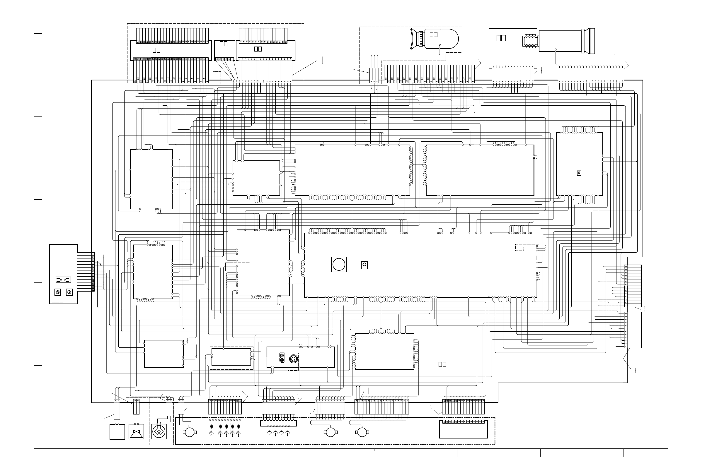
BOARD INTERCONNECTIONS
OPEN
Q2H
OEH
STH1
GND
GND
5
4
REV_SW/RVS_SW
DAC_3.2V
GND
CVF_R
CVF_G
CVF_B
LCD/CVF
(Page 4-21)
MREG_4.8
VSS
VF_LCD
LCD(MONITOR) MODULE
CLK2
CLK1
SIG_GND
07
MONITOR
HDCVF
VDCVF
HRP1
DSP_REST
PMIRROR
NC/VD_YD
NC/MV_PL_ON
MONI_B
MONI_R
MONI_G
REG_-15V
REG_3.2V
REG_4.8V
GND
REG+12V
VF_COM
GOUT
BOUT
ROUT
MONI_B
STH2RLVBRGBCLK3
MONI_G
REG_3.2V
VCOM
VEE
MONI_R
REG+12V
VDD
VGH
MREG_4.8
REG_15V
STV2
VSS
CPV
OEV
REG_4.8V
REG_4.8V
STV1
UD
CN7602
CN7601
LCD_CTL
GND/BL_GND
With C-VF MODEL
VGL
VSS
C-VF BL
(Page 4-30)
CN7801
GND/BL_GND
OPEN_SW
CN16
C_VF_PANEL
VDD
VSS
VST
VCK
STBENDWN
RGT
HST
HCK2
HCK1
BLK
BLUE
RED
GREEN
COM
0
6
0
6
C-VF
CN7701
N.C
V
8
.
4
_
G
E
VF_BLK
R
SO3
REG_3.2V
GND
HDCVF
VDCVF
REG+12V
REG_4.8V
(Page 4-31)
REG+12V
CVF_B
CVF_R
CVF_G
VF_COM
REG_3.2V
SCK3
BW/CVF
BWVFADJ
BWYGAIN
(Page 4-23)
(Page 4-25)
BW_VF_Y
VF_BL4.8
VF_BLK
GND
GND
CVF_SO3
CVF_SCK3
NC
CVF_CS
VDCVF
HDCVF
BWBLEBEL
BWYOUT
V_PLS_ON
VF_CS
VF_CTL
HRP2
VF_RPD
CN7702
CVF_SCK3
CVF_CS
SI3
CVF_SO3
3
2
1
REAR UNIT
(Page 4-36)
BATT_TERM
PC OUT DC_IN
OPEN
CN28
ADP_DC
ADP_DC
ADP_H
GND
GND
EDIT
J_GND
BATT_L
TT_BATT
BATT_+
BATT_+
BATT_CHK
YUJ40095A-2
∗
RX
∗
YUJ40095A-2
CN8
MIC
MIC_HOT
MIC_GND
OPEN
CN27
SPEAKER
DISCHG_L
BATT_CHK
BATT_+
ADP_DC
TT_BATT
ADP_H
(Page 4-19)
MCU_RST
PLI_AD
LAMP_ON
REG_CS
AREG_SO
AD_REF
SPK-
SPK+
REG
AREG_CLK
REG_4.8V
GND
DAC_3.2V
CAP_CTL
DRM_CTL
MTR_OSC
CAP_PWR
M_UNREG
DRM_PWR
LAMP_RTN
LAMP_4.5V
REG_4.8V
REG_3.2V
REG_2V
UNREG
GND
REG_-15V
REG_15V
REG+12V
REG-8-5V
AL_3.2V
Z_REG_4.8V
PLI_PWM
V_BATT
ZF_REG_4.8V
T_BATT
V OUT
(Page 4-15)
YUJ40095A-2
∗
With
CN6
DC LIGHT
MODEL
LAMP_RTN
DC LIGHT
CAM_Y
CAM_C
SC_OUT
SY_OUT
V_OUT
LAMP_4.5V
CN4
LOAD_REV
LOAD_FWD
LOADING
MOTOR
∗
YUJ40095A-2
M
CN5
F LY. E
HEAD
SPK+
SPK-
GND
GND
FE_S
OPEN
PA_SIG
SPEAKER
YTU94074-11
YTU94077-11
V_CH2_F
V_CH4_F
V_CH1_F
V_CH2_S
V_CH4_S
V_CH1_S
VIDEO HEAD
REG_4.8V
REG_3.2V
GND
V_OVL
PA_SIG
AH_GND
AH_REC
AH_PB
AE+
AECTL_HED+
CTL_HED-
AO_SIG
AO_GND
REG_3.2V
∗
V_CH3_F
V_CH3_S
V_PB_C
A_MUTE
GND
OPEN
V_PB_F
PB_CTL
V_TP_FM
V_REC_F
V_REC_C
AO_SIG_J
VTR ASP
PRE/REC
CTL_AMP
AUDIO
(Page 4-9)
FE_S
V_CH3_F
V_CH3_S
V_CH1_F
V_CH1_S
V_CH4_F
V_CH4_S
V_CH2_F
V_CH2_S
JACK (Page 4-27)
J_GND
GND
CN7
CTL_ERS-
DEW_SENS
A/C HEAD
2FSC
S_DET+
RX
REG_4.8V
CTL_HED-
SH_SIG
SCK3
SPK_VOL
FEH_ON
V_ENV
CTL_OUT
REC_CTL
A_BIAS
A_PB
APB_EP_H
A_MUTE
MIC_HOT
MIC_GND
AE-
CTL_HED+
V_FF
SO3
AE+
S OUTA/V OUT
OPEN
AH_PB
∗
AH_REC
VF_CS
VF_CTL
V_PLS_ON
V_ASP_CSV_ASP_CS
APB_EP_H
A_MUTE
SY_OUT
SC_OUT
GND
YTU94074-11
YTU94077-11
AH_GND
YTU94074-10
YTU94077-10
VD_H
FEH_ON
V_ENV
CTL_OUT
REC_CTL
A_BIAS
A_PB
SI3
REG_3.2V
S_DET_L
EDIT
∗
CLKCPU
V_OVL_B
V_OVL_A
V_PULSE
SDET_CTL
V_DSP_CS
ADP_H
EDIT
AO_SIG
AO_GND
GND
D_FG-
D_PG-
CN1
CENTER
DRUM_MOTOR
AD0
AD1
ASTB
RXD_DRV
TXD
RXD_DRV
V_OUT
D_COIL_W
AD2
AD3
LITHIUM
LAMP_ON
T_BATT
D_COIL_V
D_COIL_W
AD4
AD5
PLI_PWM
AREG_CLK
V_BATT
D_COIL_V
D_COIL_U
AD6
AD7
REG_CS
AREG_SO
D_COIL_U
AD8
AD_REF
AD9
AD10
AD11
AD12
AD13
AD14
AD15
IR_UNIT
CTL_ERS-
DEW_SENS
M_UNREG
DRM_PWR
DRM_CTL
CAP_PWR
CAP_CTL
MTR_OSC
LOAD_FWD
LOAD_REV
D_PGD_FGCENTER
D_COIL_W
D_COIL_V
D_COIL_U
GND
GND
C_FG+
CN3
MM
CAPSTAN
MOTOR
FI
CFM
OMT
R/W_L
DRUM_REF
CAP_REF
BATT_L
CAP_REF
CAP_STOP
DRUM_REF
M.MDA
(Page 4-7)
YTU94074-18
∗
YTU94077-18
C_COIL_U
C_COIL_U
CAPMR_BS
HD_H
WAIT_L
DSTB_L
OSD_CS
OSD_CLK
OSD_DATA
DRUM_FG
CAP_FG
DRUM_PG
CAP_STOP
DRUM_ON
DRUM_CLK
CAP_FR
CAP_FG
DRUM_FG
DRUM_PG
DRUM_ON
DRUM_CLK
HG_W-
C_COIL_V
C_COIL_V
C_COIL_W
C_COIL_W
MECHA
LOAD_F
CAP_FR
LOAD_F
HG_U-
LOAD_R
LOAD_R
HG_BS-
CVM_DET
UNREG
CVM_DET
HG_U+
HG_BS+
PMIRROR
OPEN_SW
R_SAF_SW
CAM_SW_C
CAM_SW_A
CAPMR_BS
REG_3.2V
C_COIL_U
C_COIL_V
C_COIL_W
HG_BS+
HG_V+
HG_W+
REV_SW
LCD_CTL
CPU (Page 4-5)
EN_SENS
STR_SENS
SUP_SENS
REEL_LED
TAPE_LED
S_VHS_SW
CAM_SW_B
TU_SENS
CAS_SW
GND
C_FG+
HG_W-
HG_U-
HG_BS-
HG_U+
HG_W+
HG_V+
HG_V-
YTU94074-14
HG_V-
YTU94077-14
UNREG
∗
REG4.8V
REG_3.2V
DSGAT
CCD_SCS
GND
01
CN2
CDS_CS
R_SAF_SW
SO3
SCK3
MAIN
GND
CAM_SW_A
CAM_SW_C
SENSOR
(Page 4-36)
CAS_SW
SUP_SENS
CAM_SW_B
V_FF
DIAL_MN
TU_SENS
REEL_LED
VDVHS
TAPE_LED
S_VHS_SW
GND
DSP_REST
EN_SENS
STR_SENS
KEY_C
VF_LCD
B_PHASE
A_PHASE
ZOOM_SW
PHOTO_SW
TRIG_SW
DIAL_AT
LENS_CS
LENS_CLK
DIAL_PB
DIAL_OF
IRIS_O/C
HALL_A/D
OPEN
EJECT_SW
IRIS_PWM
LENS_LED
LED_G
IR_DC
IR_FLICK
P0LUX_SW
TCCS_TXD
JIGCN_SW
VPP_7.8V
LED_R
PLI_AD
Z_SENS
F_SENS
AL_3.2V
KEY_A
MCU_RST
TXD
RXD
LIGHT_SW
RFRSH_SW
y10241001a_rev0
TO ZOOM UNIT (Page 4-35)
CN13
KEY_C
A_PHASE
B_PHASE
GND
GND
TRIG_SW
DIAL_MN
DIAL_AT
DIAL_OF
DIAL_PB
EIS_SW
PHOTO_SW
REG_3.2V
ZOOM_SW
YTU94074-14
YTU94077-14
∗
AL_3.2V
LED_G
LED_R
KEY_A
LIGHT_SW
REG_3.2V
KEY_C
EJECT_SW
RFRSH_SW
GND
GND
EIS_SW
CN18
TO
TOP OPE UNIT
(Page 4-35)
YTU94074-12
YTU94077-12
∗
4-44-3
HGFEDCBA
Page 19
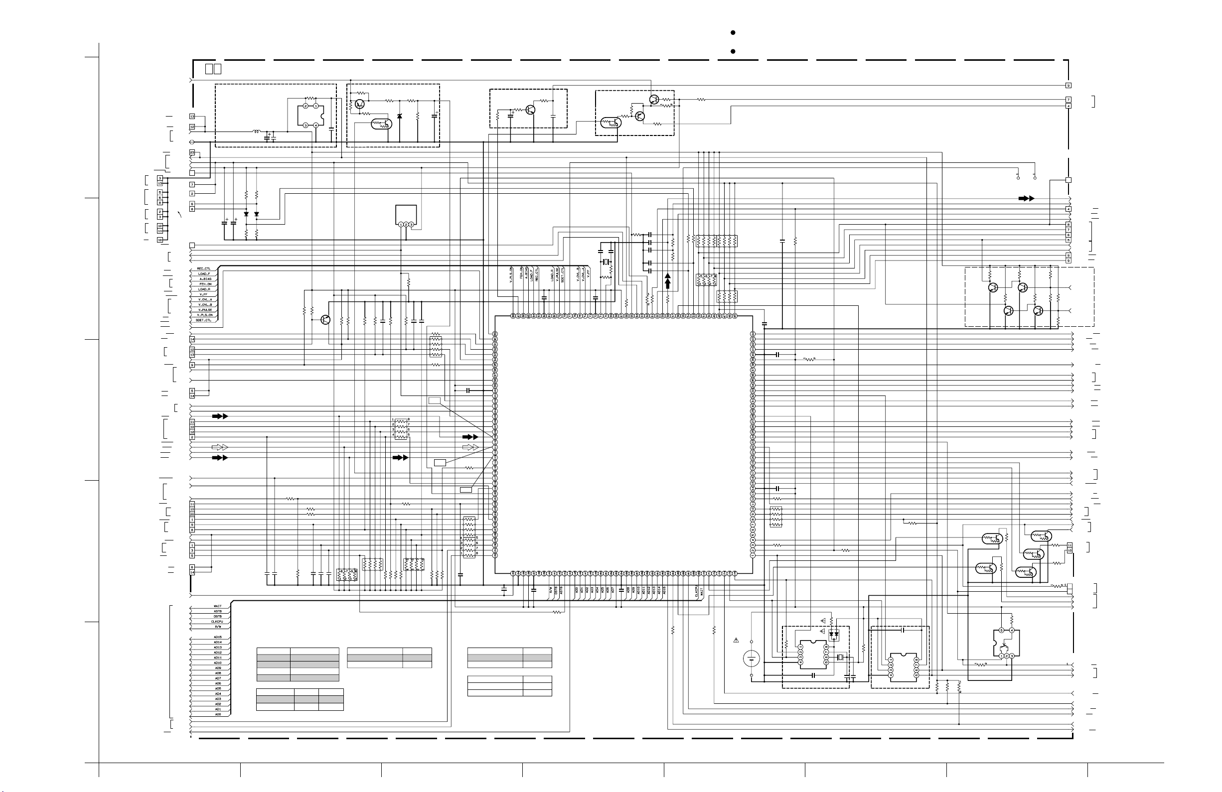
CPU SCHEMATIC DIAGRAM4.2
NOTES :
For the destination of each signal and further line connections that are cut off from
this diagram,refer to "4.1 BOARD INTERCONNECTIONS".
When ordering parts,be sure to order according to the Part Number indicated in the Parts List.
TO REG
TO REG
GND
GND
GND
GND
GND
GND
GND
GND
GND
GND
TO DSP
TO DSP
TO REG
TO REG
CN2CN2
CN25
CN18
CN13
CN7
(N.C)
(N.C)
(N.C)
AL_3.2V
AL_3.2V
AL_3.2V
MCU_RST
MCU_RST
REG_3.2V
REG_4.8V
VPP_7.8V
REG_3.2V
REG_3.2V
TU_SENS
SUP_SENS
TO SENSOR
JIGCN_SW
REMCON
PMIRROR
VF_LCD
REC_CTL
LOAD_F
A_BIAS
FEH_ON
LOAD_R
V_OVL_A
V_OVL_B
V_PULSE
V_PLS_ON
SDET_CTL
CVM_DET
ADP_H
R_SAF_SW
PEJEC_SW
B_PHASE
A_PHASE
EJECT_SW
BATT_L
JIG_CONN.
5
TO TOP OPE UNIT
JIG_CONN.
JIG_CONN.
TO SENSOR
JIG_CONN.
TO
TOP OPE UNIT
TO
ZOOM UNIT
TO A/C HEAD
JIG_CONN.
TO LCD/CVF
4
TO VTR ASP
TO M.MDA
TO VTR ASP
TO M.MDA
TO VTR ASP, DSP
TO DSP, BW/CVF
TO M.MDA
TO SENSOR
TO ZOOM UNIT
TO REAR UNIT
TO DSP
JIG_CONN.
TO M.MDA
TO DSP
TO M.MDA
TO M.MDA
TO REG
TO DSP
EJECT_SW
EJECT_SW
DRUM_FG
CAM_SW_A
CAM_SW_B
CAM_SW_C
STR_SENS
CAP_FG
CTL_OUT
DRUM_PG
HALL_A/D
DEW_SENS
F_SENS
Z_SENS
EN_SENS
LIGHT_SW
(N.C)
PLI_AD
ZOOM_SW
PHOTO_SW
S_VHS_SW
TO REG
AD_REF
WAIT_L
DSTB_L
CLKCPU
VDVHS
V_ENV
KEY_A
KEY_C
KEY_C
KEY_C
TO TOP OPE UNIT
3
TO SENSOR
TO VTR ASP
TO VTR ASP
TO F/Z/I/MDA
TO A/C HEAD
TO OP BLOCK
TO SENSOR
TO TOP OPE UNIT
2
TO ZOOM UNIT
TO SENSOR
TO TOP OPE UNIT
TO ZOOM UNIT
TO DSP
1
T_BATT
TO REG
V_BATT
TO LCD/CVF
LCD_CTL
0 1 MAIN (CPU)
UNREG
2.7V_RESET
R101
100K
CN25
CN18
AL3.2V
GND
CN25
CN25
21
CN18
CN13
CN2
C111
C112
6V
22µ/
CN25
7
C103
C104
L101
33µ
∗
T
10µ/
10V
0.01µ
10K
10K
R119
R118
D103
1SS355-X
D104
1SS355-X
6V
R120
R121
27K
27K
22µ/
V_FF
CN2
CN13
CN13
CN28
VD_H
OMT
CN18
CN25
FI
CFM
CN2
CN2
CN2
CN2
IR_DC
CN7
CN15
CN15
CN2
CN18
CN18
CN13
CN13
CN2
CN18
CN13
R126
15K
∗
∗
C135
C136
ASTB
R/W_L
AD15
AD14
AD13
AD12
AD11
AD10
AD9
AD8
AD7
AD6
AD5
AD4
AD3
AD2
AD1
AD0
# : EXCHANGE PARTS LIST
PAL(A6,C6,C7)
PAL(ALL)
NTSC(US)
NTSC(RCA)
FUNCTION
PC MODEL
NON PC MODEL
NOTES : 1. The parts with marked ( ) is not used.
2. For CPU waveforms, please refer to page 4-46.
IC104
VCC
OUT
N.C
GND
IC-PST3427U-X
C105
0.1µ
1M
∗
∗
Q112
R190
R176
18K
R167
5.6K
R168
0.4µ
27K
∗
∗
∗
C142
C138
R125
IC101MODEL ROM N0.
-38
-39
-40
-41
R182
TC1566FU
1M
∗∗
∗
C139
IC105
470K
470K
R153
R152
TO A/C HEAD
CN7
150K
R9201
CTL_ERS-
CN2
REEL_LED
TAPE_LED
JIG_CONN.
1
DIAL_MN
DRUM_REF
CAP_REF
RFRSH_SW
PLI_PWM
IRIS_PWM
DIAL_MN
DIAL_AT
DIAL_OF
DIAL_PB
OPEN_SW
REV_SW
TRIG_SW
CAS_SW
TO M.MDA
TO SENSOR
TO TOP OPE UNIT
TO REG
TO F/Z/I/MDA
TO ZOOM UNIT
TO LCD/CVF
TO ZOOM UNIT
TO SENSOR
R9202
CN2
CN25
CN18
CN13
CN13
CN13
CN13
CN13
CN2
470K
PDIAL_PB
470K
R9206
PDIAL_MN
R9205
150K
APB_EP_H
TO VTR ASP
VF_CS
TO BW/CVF
TO M.MDA
CAP_FR
TO F/Z/I/MDA
LENS_CS
TO M.MDA
CAP_STOP
CCD_SCS
TO TG/CDS
CDS_CS
TO DSP
V_DSP_CS
TO VTR ASP
V_ASP_CS
TO DSP
OSD_CS
REG_CS
TO REG
TO M.MDA
DRUM_ON
TO F/Z/I/MDA
LENS_CLK
OSD_CLK
TO DSP
OSD_DATA
TO TG/CDS
DSGAT
LAMP_ON
TO REG
LENS_LED
TO F/Z/I/MDA
IRIS_O/C
HD_H
TO DSP
DSP_REST
TO LCD/CVF, DSP, F/Z/I/MDA
TO F/Z/I/MDA
IR_FLICK
TO M.MDA
DRUM_CLK
SCK3
TO VTR ASP, DSP
F/Z/I/MDA, TG/CDS, BW/CVF
SO3
SI3
TO LCD/CVF
TXD
TO JACK
EDIT
Q107
#
CN18
LED_G
CN25
10
9
LED_R
TCCS_TXD
RXD
PLED_ECT
PLED_SIS
AL_L3.2V
RXD_DRV
AREG_CLK
AREG_SO
S_DET_L
P0LUX_SW
A_MUTE
A_PB
PDATE_SW
VF_CTL
TO TOP OPE UNIT
JIG_CONN.
(N.C)
TO JACK
TO REG
TO DSP
(N.C)
TO VTR ASP
TO VTR ASP
(N.C)
TO BW/CVF
R165
270
R164
330
R185
0R0
R104
∗
BATTERY CHECK
Q101
2SA1774/RS/-X
R105
10K
R106
560
Q102
DTC144EE-X
∗
∗
R177
R131
100K
RA112
RA105
4.7K
FUNCTION
RAE
MODEL
RAENOT
0.01µ
C113
R128
MODEL
R107
15K
RCU SENSOR
IC1801
120K
R140
2.2K
RA102
R127
1K
1K
1M
1M
R129
R141
R130
R108
24K
D102
UDZS7.5B
GND
VCC
OUT
∗
0.01µ
R178
C114
220
RA111
Q107
DTC144EE-X
R109
18K
T
C108
10V
2.2µ/
#
39K
R122
0.01µ
C116
R172
RA101
2.2K
R171
2.2K
WF1
WF2
33K
33K
470K
1M
R170
R138
R136
∗
WF3
C118
0.1µ
R169
RA103
RA104
C140
CTL_ERASE
2SC4617/QR/-X
Q103
R112
27K
10K
T
R110
P155/RTP15
V_PLS_ON
P156/RTP16
TAPE_LED
P157/RTP17
CVM_DET
P00/NMI
ADP_SW
P01/INTP0
REC_SAFE_SW
P02/INTP1
EJECT_SW
P03/INTP2
RXD
P04/INTP3
BATT_SW
P05/INTP4/ADTRG
VD
P06/INTP5/RTPTRG0
NC
P07/INTP6
OMT
VDD
SYS_3V
VSS
GND
P130/INTCP80
REMOTE_IN
P131/INTCP81
A_PHASE
P132/INTCP82
FI
P133/INTCP83
FRP
P134/TI8
B_PHASE
P135/TCLR8
CAM_SW_A
P136/TO80
CAM_SW_B
P137/TO81
CAM_SW_C
P140/INTCP90
DRUM_FG
P141/INTCP91
VDVHS
P142/INTCP92
CAP_FG
P143/INTCP93
PB_CTL
P144/TI9
DRUM_PG
P145/RTPTRG1
330
2.2K
2.2K
#
NC
P146
PHOTO_SW
P147
D_PWR_ON
P70/ANI0
V_ENV
P71/ANI1
START_SENS
P72/ANI2
EN_SENS
P73/ANI3
BATT
P74/ANI4
IR_DC
P75/ANI5
DEW_SENS
P76/ANI6
FOCUS_SENS
P77/ANI7
ZOOM_SENS
P80/ANI8
HOLE
P81/ANI9
KEY_A
P82/ANI10
LIGHT_SW
P83/ANI11
KEY_C
P84/ANI12
PLI_AD
P85/ANI13
ZOOM_SW
P86/ANI14
T_BATT
P87/ANI15
V_BATT
AD_REF
C115
FUNCTION
With RCU
Without RCU
FUNCTION
C-VF MODEL
BW-VF MODEL
AVREF
0.1
R111
C109
10/
10V
P154/RTP14
R153/RTP13
FEH_ON
CTL_ERASE
SYS_3v
GND
AVDD
AVSS
P152/RTP12
P151/RTP11
LOAD_F
A_BIAS_L
GND
SYS_3V
VSS
VDD
∗
IC1801
PIC-26043S
∗
C140
∗
22p
330
C110
100p
C121 C122
0.1µ 0.1µ
∗
VSS
VDD
GND
P150/RTP10
P107/RTP07
P106/RTP06
P105/RTP05
P104/RTP04
SYS_3V
LOAD_R
V_PULSE
REC_CTL
SDET_CTL
S_VHS_SW
ASTB
DSTB_L
R/W_L
HBEN
LBEN
P96/HLDRQ
P95/HLDAK
P94/ASTB
P93/DSTB/RD
P92/RW/WRH
P91/UBEN
P90/LBEN/WRL
C134
0.1µ
R157
0R0
NC
P103/RTP03
TBC_VD
AD0
LCD_CTL
P40/AD0
P102/RTP02
P41/AD1
P101/RTP01
V_OVL_BCD
AD1
P42/AD2
C123
10p
VSS
V_FF
P100/RTP00
V_OVL_A
AD3
AD2
P44/AD4
P43/AD3
TAPE_LED
Q104
DTC144EE-X
C124
10p
X101
R144
R143
NAX0251-001X
1M
∗
X2
X1
VDD
X2
X1
GND
SYS_3V
AD7
AD6
AD5
AD4
P47/AD7
P46/AD6
P45/AD5
R114 R115
820
2SA1774/RS/-X
220
R145
2.2K
XT2
XT1
RESET
XT2
XT1
NC/VPP
RESET(L)
#
IC101
UPD703039-XXX
UPD70F3040-XXX
AD8
GND
SYS_3V
P51/AD9
P50/AD8
BVSS
BVDD
∗
C133
0.1µ
5.6K
R113
Q105
R142
10K
P167/HSOUT1
VF_LCD
VPP7.8V
AD10
AD9
P52/AD10
C127
C128
C119
P166/HSOUT0
PMIRROR
AD11
P53/AD11
∗
0.033µ
C129
C120
0.01µ
330
R189
P165/VSOUT
JIGCN_SW
AD12
P54/AD12
∗
Q106
100
0.47µ
0.033µ
0.01µ
2.2K
R146
P163/PWM3
P162/PWM2
P164/CSYNCIN
PLI_PWM
REFRESH_SW
AD14
AD13
P57/AD15
P56/AD14
P55/AD13
R116
2.2K
2.2K
R147
P161/PWM1
IRIS_PWM
DRUM_REF
VF_CTL
AD15
P60/A16
4.7K
P160/PWM0
CAP_REF
PDATE_SW
P61/A17
R149
R148
P177/KR7
P62/A18
2.2K
R158
R181
0R0
REEL_LED
2.2K
2.2K
R151
R150
P176/KR6
P175/KR5
P174/KR4
TBC_CTL
SUPSENS
RTC_INTR
A_PB
PLED_SIS
P65/A21
P64/A20
P63/A19
R117
1k
P173/KR3
DIAL_MN
TUPSENS
CLKOUTNCA_MUTE
CLKOUT
P172/KR2
WAIT
470K
RA109
RA108
P171/KR1
DIAL_AT
WAIT_L
P110
2.2K
P197
P170/KR0
DIAL_PB
DIAL_OF
P0LUX_SW
PLED_ECT
P112
P111
2.2K
R159
470K
RA110
CAS_SW
P196
P195
REV_SW
APB_EP_H
TRIG_SW
OPEN_SW
CAP_FR
LENS_MDA_CS
SYS_3V
CAP_STOP
CCD_CS
CDS_CS
V_DSP_CS
V_ASP_CS
EEPROM_CS
OSD_CS
REG_CS
RTC_CS
DRUM_ON
LENS_MDA_CLK
OSD_CLK
OSD_DATA
232C_EN
DRUM_CLK
LAMP_ON
LENS_LED
IRIS_O/C
SYS_3V
IR_FLICK
P25/SCK3/ASCK1
P22/SCK2/SCL1
P15/SCK1/ASCK0
DSP_RST
P12/SCK0/SCL0
AL_CLK
AL_SI
S_DET_L
NC
P11/SO0
P10/SI0/SDA0
P113
LITHIUM
J101
QAB0050-001
2.2K
VF_CS
P127/TI11/TO11
P126/TI10/TO10
P125/TI7/TO7
P124/TI6/TO6
P122/SCK4
P37/TI5/TO5
P36/TI4/TO4
DSGAT
LED_G
LED_R
P27/TI3/TO3
P26/TI2/TO2
SCK3
P24/SO3/TXD1
P23/SI3/RXD1
SCK2
P20/SI2/SDA1
P14/SO1/TXD0
P13/SI1/RXD0
AL_SO
RA107
GND
P123/CLO
P121/SO4
P33/TIO11
P32/TIO10
P31/TIO01
P30/TIO00
GND
RXD
TP102
TP101
R166
C144
1M
R9204
Q9202
470K
2SC4617/QR/-X
R9209
Q9204
470K
2SC4617/QR/-X
470K
R9203
Q9201
2SC4617/QR/-X
Q9203
R9208
470K
2SC4617/QR/-X
P194
C141
P193
P192
P191
P190
VSS
VDD
P187
P186
NC
P185
P184
P183
P182
P181
P180
C131
∗
R188
0.1µ
4.7K
OPEN
NC
P120/SI4
P35/TO1
P34/TO0
HD
VSS
VDD
TO2
SO3
SI3
P21/SO2
SO2
SI2
TXD
C132
∗
0.1µ
R163
10K
RA106
330
R102
IC103
RS5C314-X
R154
2.2K
CE
SCLK
SIO
Vss
OSCIN
OSCOUT
R103
1K
R156
D101
SB007W03Q
VDD
X102
INTR
NAX0325-001X
C125
0.01
R155
470K
C126
C143
10p
3p
RTC
4.7K
R162
C107
0.01µ
AT25080N-10SC-X
IC102
Vcc
CS
HOLD
SO
SCK
WP
SI
Vss
EEPROM
R179
Q113
∗
∗
Q109
Q114
∗
R184
∗
R160
100K
R139
100K
470K
R9207
DTC114EE-X
R180
Q108
∗
DTC114EE-X
#
R182
#
IC105
y10242001a_rev0
ABCD EFGH
4-64-5
Page 20
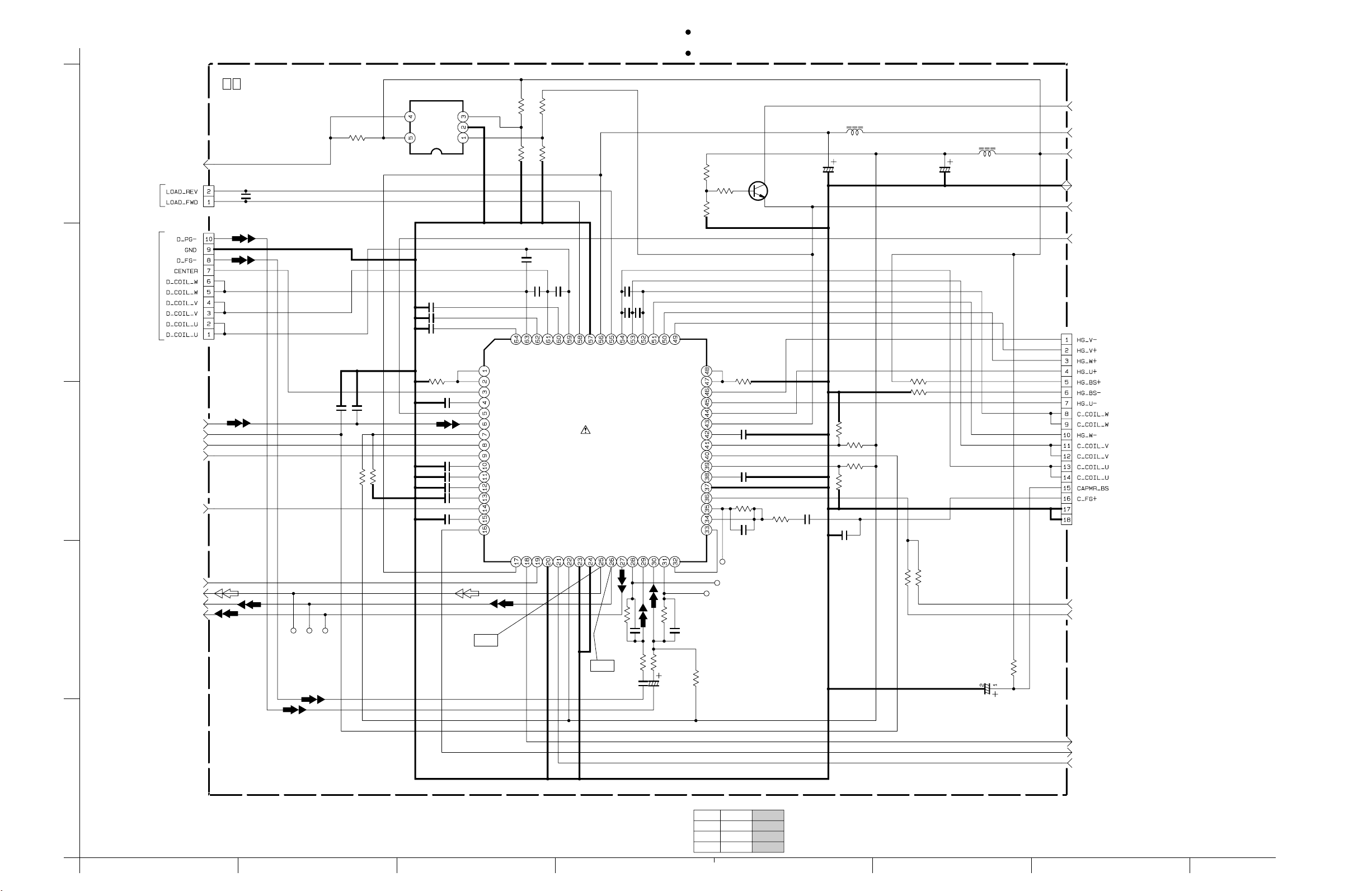
M.MDA SCHEMATIC DIAGRAM4.3
NOTES :
For the destination of each signal and further line connections that are cut off from
this diagram,refer to "4.1 BOARD INTERCONNECTIONS".
When ordering parts,be sure to order according to the Part Number indicated in the Parts List.
5
TO
LOADING MOTOR
TO
DRUM MOTOR
4
3
2
TO CPU
CVM_DET
TO CPUTO CPUTO CPU
DRUM_REF
CAP_REF
LOAD_F
LOAD_R
TO CPU
DRUM_ON
TO CPU
DRUM_CLK
CAP_FG
DRUM_PG
DRUM_FG
0 1 MAIN (M.MDA)
C1625
0.1
CN4
CN1
TL1606
TL1607
C1627
∗
TL1608
R1628
10k
C1626
15k
R1603
∗
15k
R1604
IC1602
TA75S393F-X
IN (+)
OUT
GND
VCC
IN (-)
C1622
∗
C1623
∗
C1624
∗
R1601
0.33
0.1
C1601
1
C1602
#
C1603
#
C1604
#
C1605
0.1
C1606
WF1
YATC
YCS
YCOM
YPCI
YVM
YEC
VCONT
IN1
IN2
VREF
YSUL2
YSUL1
AGC
YSTB
YPCS
YSW
10k
R1626
22k
R1627
C1619
0.1
C1618
0.1 0.1
YM3
YMI3
UNREG
CSW
R1624R1625
C1617
YM2
YMI2
YCLK
YGNDFCVCC
33k12k
YM1
YMI1
OUT1
IC1601
LB11951WA-MPB
GND
VB
LPGND
CFG2
CFG
C1608
0.0033
0.1
C1615
OUT2
YPG
R1606
CM1
YFG
C1616
CM2
YFGO
100k
0.1
C1614
CM3
YFGI
0.1
H3-
YPGI
R1608
H3+
CFG2O
YPGO
150k
R1621
330
R1622
220
H2+
CATC
CCS
H2-
H1-
H1+
CVM
CPCI
CTL
CEC
CECR
CPCS
CGND
CRSF
CFG2I
CFG1I
CFG1O
C1610
680P
TL1602
R1623
0Ω
C1613
C1612
R1610
TL1601
R1602
0.33
C1628
100P
TL1603
0.033
1
100k
Q1601
2SC4617/QR/-X
R1609
C1611
0.1
470
/16
C1621
10
L1601
NQL144M-1R0X
∗
R1614
100k
R1613
15k
R1611
15k
R1612
C1629
∗
R1615
R1616
15k
R1618
1.5k
1.5k
15k
R1617
C1620
TO REG
UNREG
M_UNREG
L1602
NQL144K-100X
/10
TT
10
REG_3.2V
GND
CAP_PWR
DRM_PWR
TO
CAPSTAN MOTOR
CN3
GND
GND
TO CPU
CAP_STOP
CAP_FR
T
C1630
10
/6.3
R1620
220
WF2
C1607
0.47
1k
R1605
T
470
R1607
C1609
/10
10
330k
R1619
TO REG
CAP_CTL
DRM_CTL
MTR_OSC
1
NOTES : 1. The parts with marked ( ) is not used.
2. For M.MDA waveforms, please refer to page 4-46.
∗
# : EXCHANGE PARTS LIST
NTSC
0.0047
C1603
C1604
0.0047
C1605
0.033
PAL
0.01
0.01
0.01
4-84-7
y20156001a_rev0
HGFEDCBA
Page 21
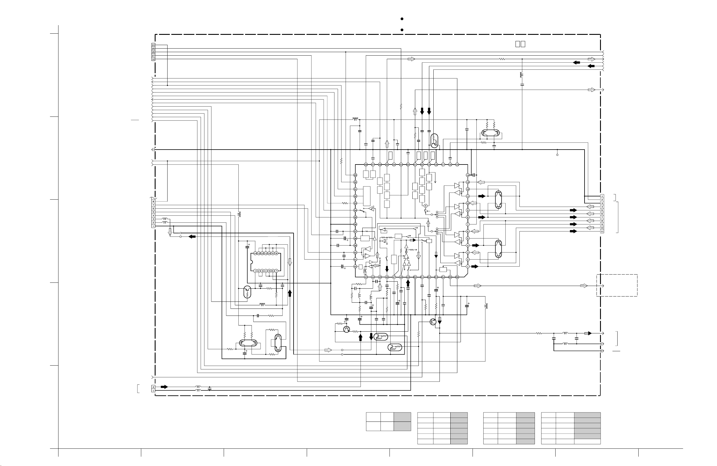
VTR ASP SCHEMATIC DIAGRAM4.4
NOTES :
For the destination of each signal and further line connections that are cut off from
this diagram,refer to "4.1 BOARD INTERCONNECTIONS".
When ordering parts,be sure to order according to the Part Number indicated in the Parts List.
JIG_CONN.
CN25
V_FF
V_TP_FM
V_OVL
PB_CTL
AO_SIG_J
5
TO DSP
4
3
2
TO CPU
FEH_ON
V_ENV
V_FF
SCK3
SO3
V_ASP_CS
CTL_OUT
REC_CTL
A_BIAS
A_PB
A_MUTE
APB_EP_H
SPK_VOL
TO REG
GND
REG_4.8V
REG_3.2V
TO A/C HEAD
REG_4.8V
CTL_HED-
CTL_HED+
AE-
AE+
AH_PB
AH_REC
AH_GND
R3502
C
1k
L3502
22µ
C3512
C3513
10
0.022
C3515
0.01
C3514
1
15k
2Fsc
CR
OVL
SW30
CTL
GND
OUT
CTL
Vcc
DET
CR
1/2
ENV OUT
DEMOD
HPF ENV
SERIAL I/O
DC
CONT
BG
SP
ON
∗
C2040
L2022
#
T
C2039
#
C2023
C2022
#
R2024
L2023
#
1
T
/6.3
C2026
0.0022
C2024
#
R2025
R3508
CLK
T
R3506
1000p
/6.3
1k
T
C1204
C2021
#
R2022
330k
Q2071
DATA
LOAD
CTL
OUT
REC IN
MONI
DC
DET
0.01
CTL-
R2021
10k
R2023
#
T
C2071
/6.3
10
R2072
5.6k
CN7
L2004
#
L2005
0Ω
JP2001
JP2002
L2001
47µ
C2001
10
/6.3
T
DTA114TE
Q2001
R2002
Q2008
PUMT1
R2005
2.7k
C2004 R2012
/6.3
22
T
5A
6A1Y
6Y
Vcc
IC2001
MC74AC04DT
1A2A3A
2Y
C2003
330p
R2001
100k
L2003
47µ
C2005
1
R2004
6803.3k
5Y
R2003
R2011
C1201
C1202
10
/6.3
4A
4Y
GND
3Y
C2002
TF
0.018
1k
R2006
1k
100
Q2007
PUMX1
100
C1205
R2071
47k
10
C1206
2SC4617/QR/
JP2004
JP2003
REC ON
C2025
#
82k
PB FM
FM
1
P EQ G EQ
AGC
TRAP
WF4
FM
Vcc
DET
C2027
Q2021
DTC144EE
Q2022
DTC144EE
R2030
0.47
C2036
C3511
PRE OUT
100k
C2028
T
/6.3
10
1
C2038
R3501
#
DET
LINE MUTE
MUTEREC
REC
C2029
0.47
1
C3510
Audio
Y
C
R3901R3902
R3903
1.8k
L2021
47µ
Q3502
HN1C01FU/G
Q3501
HN1C01FU/G
10100
C3901
FEFEFE
CTLINOUTFMGND
CH2
CH2
CH4
CH4
CH1
CH1
CH3
CH3
C3902
P/R
GND
P/R
Vcc
IC3501
HA118224F
C2035
22
T
/6.3
C3506
0.01
C3507
C3508
0.01
0.01
Q3505
WF2
FM
REC C
LPF
EQ
REC C
LPF
C2032
0.0047
1k
R2027
Q2023
2SC4617/QR/
R2031
3.3k
Buff
SERIAL
C2033
WF1
N/S
CTL
/6.3
4.7
1k
R2028
#
C3903
3p
CTL
VCA
Audio
Vcc
T
0.1
C2034
C3509
#
WF3
0.1
REC
PB C
LUG READ
LPFHPFTRAP
A/D
LPFLPF
PB
GND
0.1
C2031
0 1 MAIN (VTR ASP)
#
R3507
L3503
#
C3516
#
Q3901
HN1A01FU/G
R2051
JP3501
L2051
Ω
1k
0
C2052 C2051
L2052
∗
0Ω
TO DSP
V_OVL
2FSC
C
V_PB_F
V_REC_F
V_REC_C
S_DET+
TO TG/CDS
V_PB_C
CN5
TO
GND
FE_S
FLY.E HEAD
GND
V_CH2_S
V_CH2_F
V_CH4_S
TO
V_CH4_F
VIDEO HEAD
V_CH1_S
V_CH1_F
V_CH3_S
V_CH3_F
TO SPEAKER
PA_SIG
Y
C
N.C
AO_SIG
TO
∗
AO_GND
GND
JACK
TO RE G
TO DSP
SH_SIG
CN8
MIC_HOT
TO MI C
MIC_GND
NOTES : 1. The parts with marked ( ) is not used.
1
2. For VTR ASP waveforms, please refer to page 4-46.
ABCD EFGH
L2071
0
L2072
C2072
Ω
0.0022
0Ω
∗
# : EXCHANGE PARTS LIST
[VIDEO]
VHS
SVHS
Q3505
MODEL MODEL
DTC144
∗
R3507
L3503
EE
C3516
R3501
C3509
NTSC PAL
100
0
5.6
∗
10p
∗
220
0
220p
∗
R2023
R2024
C2021
C2022
C2024
NTSC PAL
[AUDIO]
150 82
13k 18k
0.0068 0.01
10
15/6.3 /6.3
µµ
0.0012 0.001
L2004
L2022
L2023
C2039
y20158001a_rev0
NTSC PAL
0
NQR0403-003X
Ω
0
NQR0403-003X
Ω
0
NQR0406-003X
Ω
∗
33
p
4-104-9
Page 22
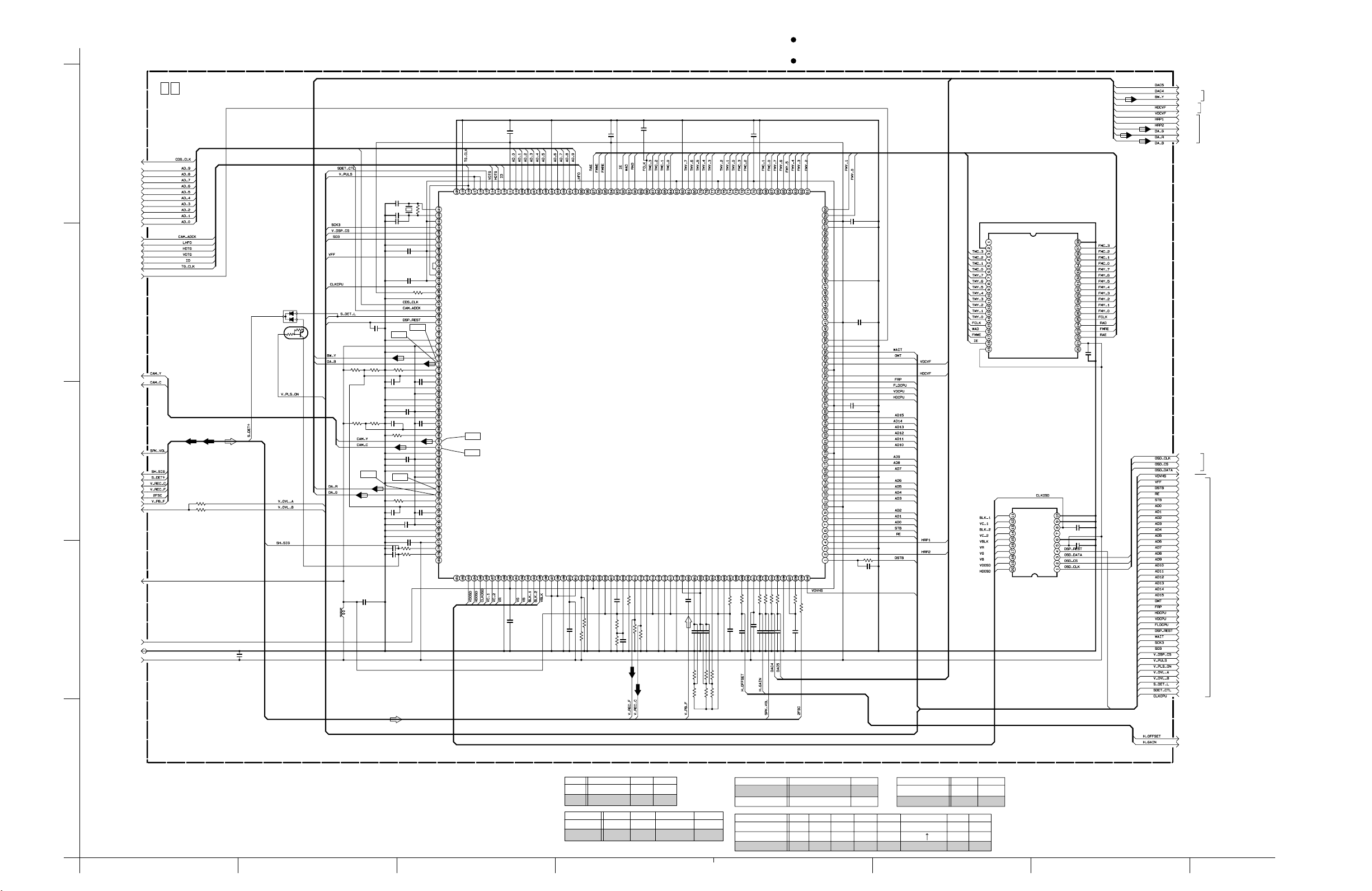
DSP SCHEMATIC DIAGRAM4.5
NOTES :
For the destination of each signal and further line connections that are cut off from
this diagram,refer to "4.1 BOARD INTERCONNECTIONS".
When ordering parts,be sure to order according to the Part Number indicated in the Parts List.
TO LCD/CVF,
BW/CVF
0 1 MAIN (DSP)
VDD10
IO
AVBB
∗
0.1
C4029
R4017
R4018
IE
WAD
GND9
CCOMPFMY
IRSETFMY
VREFFMY
0.1
R4019
∗
0.1
C4030
Y
8.2k
RAD
FMOUT
R4020
C
C4006
NC
FMWR
RECCOUT
470
CH
10p
TMY[5]
TMY[6]
TMY[7]
REFBOTI
CML
PBFMI(AINT)
0.1
C4033
0.1
C4034
0.1
TMY[4]
REFTOPI
C4035
0.1
TMY[3]
AVSS
VDD8
CORE
AVDD
180
R4021
MCLK
AVSS
TMC[3]
AVDD
TMC[2]
AVBB
TMC[1]
AVBB
TMC[0]
AVDD
VDD9
CORE
AVSS
GND8
AINC
C4032
TMY[2]
AVBB
R4026
0.1
TMY[1]
STC
56k
TMY[0]
EOC
C4036
C4037
FMC[3]
PWMOUT1
100k
R4027
0.1
C4005
FMC[2]
GND17
CORE
IO
0.1
0.1
VDD7
VDD20
R4028
C4038
C4039
GND7
PWMOUT2
R4029
100k
100k
0.1
C4040
FMC[0]
FMC[1]
PWMOUT3
PWMOUT4
R4030
R4031
#
##
0.1
C4041
FMY[6]
FMY[7]
CORE
CORE
CORE
PWMOUT5
GND
#
C4042
FMY[5]
IO
DICK
FMY[2]
FMY[3]
FMY[4]
FMY[1]
FMY[0]
IO
VDD6
GND6
HDDSC
VDDSC
FLDDSC
CLKDSC
DSC[3]
DSC[2]
DSC[1]
DSC[0]
GND5
DSY[7]
DSY[6]
DSY[5]
DSY[4]
DSY[3]
DSY[2]
IO
VDD5
DSY[1]
DSY[0]
PBLK
GND4
BUSY
OMT
VDCVF
VDD4
HDCVF
FRP
FLDCPU
VDCPU
HDCPU
VDD3
GND3
BUS[15]
BUS[14]
BUS[13]
BUS[12]
BUS[11]
BUS[10]
VDD2
BUS[9]
BUS[8]
BUS[7]
GND2
BUS[6]
BUS[5]
BUS[4]
BUS[3]
VDD1
BUS[2]
BUS[1]
BUS[0]
ASTB
RW
HRP1
GND1
HRP2
DSTB
DCKO
FSC2OUT
VREFO
560
R4032
3.9k
R4033
CH
C4043
10p
C4003
C4004
0.1
C4002
NC
GND
D11
D10
D9
D8
D7
D6
IC4002
D5
D4
D3
D2
D1
D0
0.1
0.1
R4001
1k
C4001
SWCK
RSTW
WE
IE
VCC
BLK1
VC1
BLK2
VC2
VBLK
VR
VG
VB
VSYNC
HSYNC
IC4003
GND
Q11
Q10
Q9
Q8
Q7
Q6
Q5
#
Q4
Q3
Q2
Q1
Q0
SRCK
RSTR
RE
OE
VCC
NC
C4044
#
GND
TEST
OSCIN
OSOUT
CKOUT
CH
C4046
220
p
NC
1
C4045
VDD
PCL
DATA
CS
CLK
#
/16
∗
1.8k
∗
R4024
R4036
R4022
∗
2.2k
R4037
R4023
R4025
∗
C4048
0.1
5
4
3
2
TO TG/CDS
CDS_CLK
AD_9
AD_8
AD_7
AD_6
AD_5
AD_4
AD_3
AD_2
AD_1
AD_0
CAM_ADCK
LHFO
HDTG
VDTG
ID
TG_CLK
PBLK
#
D4001
C4031
Q4001
#
TO V OUT
CAM_Y
CAM_C
Y
R4034
R4035
C
3.3k
3.3k
L4001
C4047
0.1
TO VTR ASP
SPK_VOL
TO VTR ASP
SH_SIG
S_DET+
V_REC_C
V_REC_F
2FSC
V_PB_F
V_OVL
TO V OUT,
LCD/CVF
DAC_3.2V AD13
TO REG
REG_2V
GND
REG_3.2V
1
R4005R4006
∗
∗
∗
∗
R4007R4008
WF6
R-Y
Y
C4024
C4026
10µ
22
C4009
10p
CHCH
C4010
10p 1M
CH
C4011
WF2
Y
R4004
15k
C4013
0.1
C4017
0.1
R4009
15k
C
WF5
R4010
#
15k
0.1
C4019
C4023
#
C4025
#
X4001
R4002
∗
0.1
C4008
C4012
0.1
R4003
56k
WF1
B-Y
C4014
0.1
0.1
C4015
C4016
0.1
Y
C4018
0.1
C4020
#
0.1
#
C4021
0.1
0.1
#
R4013
R4014
##
XIN
XOUT
VDD12
SDCK
SLD
STD
GND12
VDD13
SW30
DOCK
DCKI
CLKI
VDD14
CLKCPU
SCLEARI
GND13
AD1_CK
CAMADCK
SVHSOUT
CLR
SCAN
DCTEST
AVBB
AVDD
AVSS
BWYO
BYOUT
IRSETBWY
VREFBWY
CCOMPBWY
AVBB
AVDD
AVSS
AVSS
AVDD
AVBB
CCOMPC
VREFC
IRSETC
YOUT
COUT
AVSS
AVDD
AVBB
AVBB
AVDD
AVSS
RYOUT
Y2OUT
IRSETRY
VREFRY
CCOMPRY
AVBB
AVDD
AVSS
GND
VDD16
KOUT
CSYNC
AD2_CK
GND11B
CORE
CORE
CORE
IO
SCBLKO
GND11
WF4
ACDELAYOUT
CAMCK
WF3
VDOSD
ADDV
HDOSD
SDPRD
HDMASK
CLKOSD
VC1
VDTG
VC2
HDTG
VR
ID
CORE
GND14
0.1
VDD11
IO
VDD17
C4027
ADIN[2]
ADIN[1]
ADIN[0]
VGVBBLK1
ADIN[3]
BLK2
ADIN[4]
VBLK
ADIN[5]
TSEL[1]
GND10
TSEL[2]
ADIN[6]
TSEL[3]
ADIN[7]
GND15
C4028
0.1
ADIN[8]
IO
VDD18
C4007
NC
RAE
WAE
LHFO
FMRE
FMWE
ADIN[9]
IC4001
JCY0140-3
NTSC_L
CORE
TSEL[0]
TVSELO
GND16
VDD19
AVSS
AVDD
#
R4016
R4015
#
Y
R-Y
B-Y
BWYGAIN
BWBLEVEL
TO BW/CVF
BWYOUT
HDCVF
TO LCD/CVF,
VDCVF
BW/CVF
HRP1
HRP2
Y
GOUT
ROUT
BOUT
OSD_CLK
OSD_CS
OSD_DATA
VDVHS
V_FF
DSTB_L
R/W_L
ASTB
AD0
AD1
AD2
AD3
AD4
AD5
AD6
AD7
AD8
AD9
AD10
AD11
AD12
AD14
AD15
OMT
CFM
HD_H
VD_H
FI
DSP_REST
WAIT_L
SCK3
SO3
V_DSP_CS
V_PULSE
V_PLS_ON
V_OVL_A
V_OVL_B
S_DET_L
SDET_CTL
CLKCPU
TO
LCD/CVF
TO CPU
TO CPU, F/Z/I/MDA
TO CPU
TO
F/Z/I/MDA
H_OFFSET
H_GAIN
1
NOTES : 1. The parts with marked ( ) is not used.
2. For DSP waveforms, please refer to page 4-46.
∗
# : EXCHANGE PARTS LIST
PAL
VHS MODEL
MODELSVHS
QAX0709-001
QAX0708-001
X4001 R4015 R4016
0
R4014 C4025 Q4001 D4001
∗∗ ∗ ∗
10k 0.1 DTC144EE-X DAN222-X
NTSC
R4013
0∗
∗
MEMORY
MODEL
MEMORYNON
MODEL
JVC
C-VF
MODEL
JVC
OTHER
MODEL
MODELPANASONIC
IC4002
Z4C2973-32-X
R4010
R4030 R4031C4041 C4042
15k
∗∗
∗
∗∗∗∗
1k 1k
C4044
µ
1
∗∗
1k
11
NON PB SNAP SHOT
1
µ
PB SNAP SHOT
IC4003
µ
PD6467GR-512-X
PD6467GR-508-X
µµµ
C4019
C4024
∗∗
0.11k
C4020
0.1µ
0.1µ
∗
∗
4-124-11
y10243001a_rev0
HGFEDCBA
Page 23
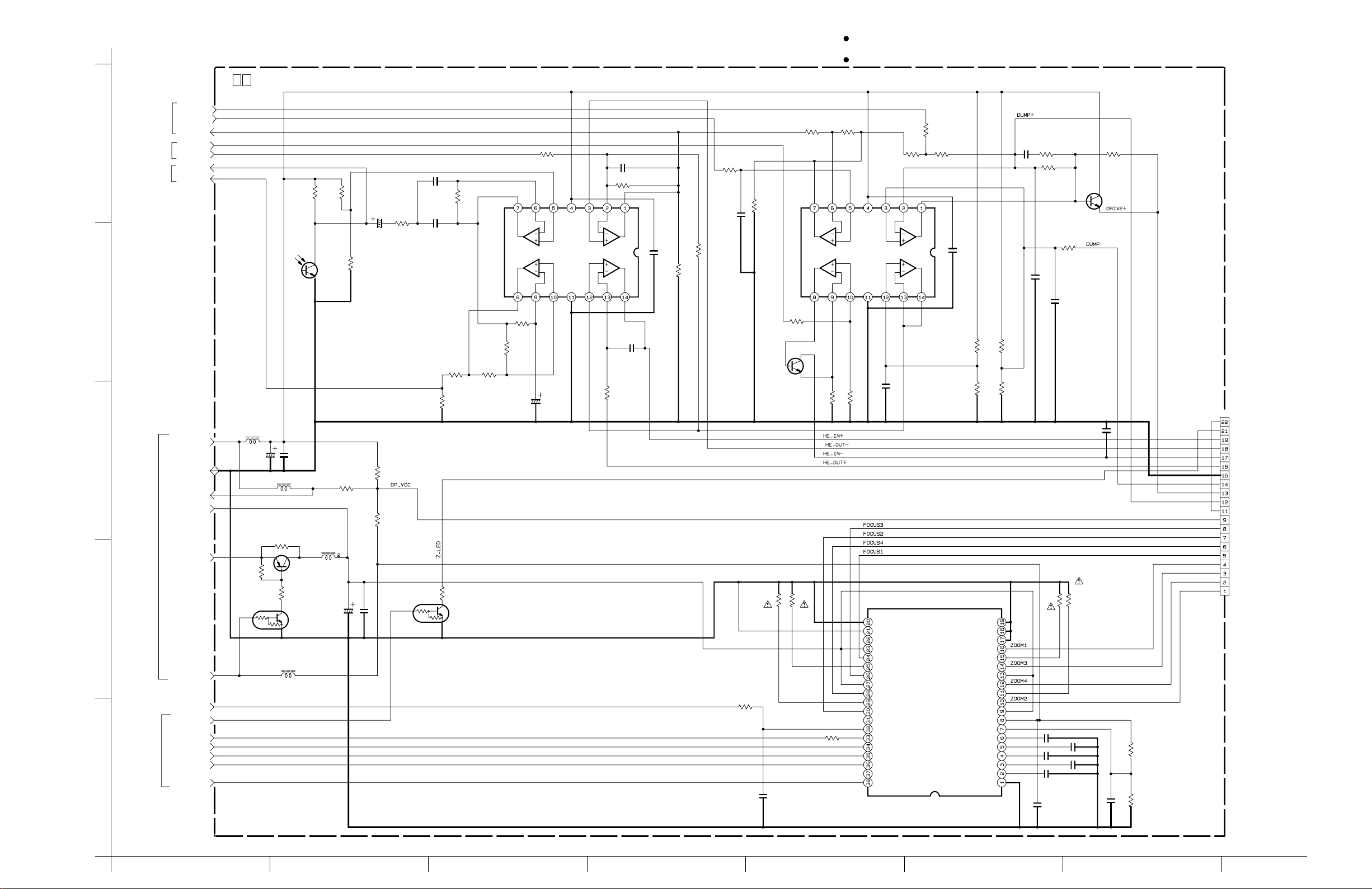
F/Z/I/MDA SCHEMATIC DIAGRAM4.6
NOTES :
For the destination of each signal and further line connections that are cut off from
this diagram,refer to "4.1 BOARD INTERCONNECTIONS".
When ordering parts,be sure to order according to the Part Number indicated in the Parts List.
0 1 MAIN (F/Z/I/MDA)
IRIS_O/C
TO CPU
5
TO DS P
TO CP U
4
3
TO REG
2
TO CP U
1
IRIS_PWM
HALL_A/D
H_GAIN
H_OFFSET
IR_DC
IR_FLICK
REG_4.8V
GND
Z_REG_4.8V
ZF_REG_4.8V
UNREG
REG_3.2V
TO DS P
VDVHS
LENS_LED
LENS_CS
SO3
SCK3
LENS_CLK
DSP_REST
L4201
NQR0006-001X
C4201
2.2/50
R4510
∗
R4511
L4502
R4509
∗
NQR0006-001X
22µ
∗
L4501
C4202
Q4503
Q4502
R4207R4206
100k10k
R4210
1M
C4205
0.01
R4205
C4203
0.1
1M
0.1
R4211
C4252
R4214
4.7k
3K
R4258
100K
R4262
C4256
/16
10
R4259
68K
Q4251
RPM-22PB
WHITE
BALANCE
(
)
SENSOR
0.1
R4512
L4503
∗
R4516
∗
0R0
R4513
∗
R4257
8.2K
C4253
0.015
C4254
0.015
R4251
1.8K
R4252
10K
820K
R4256
BA10324AF-XE
IC4201
R4253
R4254
680K
R4255
C4251
3.3
2.2K
10K
10k
/50
R4201
100k
R4209
R4208
C4206
0.1
24k
4.7k
BA10324AF-XE
IC4202
0R0
R4202
Q4201
2SC4617/QR/-X
330
R4204
22k
R4203
1
C4210
∗
C4513
R4503R4504
6R86R8
P_GND
EXP3
EXTa
Vm1
A1
FBa
A2
Vm2
B1
FBb
B2
EXTb
R4507
10K
VD
LATCH
SD ATA
SCLK
OSCin
OSCout
RESET
∗
270
Q4501
DTC114EE-X
R4505
R4508
10K
C4512
100
/16
∗
0.1
C4504
R4216
10k
R4215
R4217
1k
68k
C4209
0.1
UPD16835AGS-X
IC4501
R4223
EXP2
EXP1
EXP0
FBc
Vm4
FBd
Vm3
Vdd
Vref
FILd
FILd
FILc
FILc
FILb
FILb
FILa
FILa
Cosc
GND
33k
C1
C2
D1
D2
22k
R4224
R4221
330k
R4222
150k
C4208
0.1
R4218
R4219
C4211
∗
R4502
C4511
0.1
6R8
100k
R4220
C4509
1000p
C4507
1000p
C4505
33p
1K
C4212
∗
Q4202
2SC4617/QR/-X
1.5k
0.01
C4207
R4501
6R8
C4508
1000p
C4506
1000p
R4225
∗
0.1
C4510
R4514
22K
R4515
1.8K
TO OP BLOCK
CN15
Z_L_VCC
ZOOM_LED
HE_IN+
HE_OUT-
HE_IN-
HE_OUT+
GND
DUMP-
DRIVE+
DUMP+
F_LED
OP_VCC
FOCUS3
FOCUS2
FOCUS4
FOCUS1
ZOOM1
ZOOM3
ZOOM4
ZOOM2
NOTE : The parts with marked ( ) is not used.
ABCD EFGH
∗
4-144-13
y20157001a_rev0
Page 24

V OUT SCHEMATIC DIAGRAM4.7
NOTES :
For the destination of each signal and further line connections that are cut off from
this diagram,refer to "4.1 BOARD INTERCONNECTIONS".
When ordering parts,be sure to order according to the Part Number indicated in the Parts List.
TO REG
REG_4.8V
TO DSP
5
4
3
DAC_3.2V
TO DSP
CAM_Y
TO REG
GND
R4704
1.2k
C4704
C4702
27p
∗
R4702
680
R4703
Q4701
2SA1774/QR
15p
C4703
Y
1.1k
R4701
1µ
C
Y
∗
C4701
MUTE
GND
GND
IC4701
#
CIN
GND
YIN
IC4702
#
6dB
Vcc
OUT
SAG
VCC
75
VCC
L4701
22µ
WF1
C4708
C4709
0 1 MAIN (V OUT)
JIG_CONN.
CN25
V_OUT
C4706
/4
100µ
22µ
/6.3
0.1
/6.3V
T
10µ
C4707
#
C4714
C4713
#
R4706
R4712
68
Y+C
TO JACK
V_OUT
#
TO JACK
SY_OUT
GND
NC
R4710
Q4702
C4717
1.2K
2SA1774/QR
C4705
C
0.01
# : EXCHANGE PARTS LIST
C4716
27p
2
TO DSP
CAM_C
C
R4707
750
NOTES : 1. The parts with marked ( ) is not used.
2. For V OUT waveform, please refer to page 4-46.
R4709
680
∗
15p
R4708
∗
Chroma
MUTE
1
VHS MODEL
6dB
75
6dB
NC
75
#
C4715
IC4701 IC4702 R4712 R4713 C4713 C4714 C4715
MM1512XN
∗∗∗∗∗∗
#
R4713
TO JACK
SC_OUT
y30153001a_rev0
SVHS MODEL
∗
4-164-15
BA7665FS 68 68 0.0122/6.3 100/4
HGFEDCBA
Page 25

TG/CDS SCHEMATIC DIAGRAM4.8
NOTES :
For the destination of each signal and further line connections that are cut off from
this diagram,refer to "4.1 BOARD INTERCONNECTIONS".
TO CCD
When ordering parts,be sure to order according to the Part Number indicated in the Parts List.
CN5301
CN22
5
4
3
H1
H2
V4
V3
V2
V1
GND
GND
GND
CCD_OUT
CCD_HV
SUB
CCD_LV
RG
0 1 MAIN (TG/CDS)
CCD
C5231
R5217
∗
C5230
0.1
100k
C5229
1µ
C5218
0.1
/25
NC
NC
NC
NC
VM
V2
V4
V1
VH
V3
SUB
VL
TESTEN
NC
10p
C5232
NC
VSS4
H2
10p
C5233
H1
VDD4
IC5202
JCY0098
TG+V_DRIVER
0.1
C5228
VDD3
NC
RG
C5227
0.1
10p
C5234
XRS
C5235
10p
XSHP
XSHD
C5236
10p
VSS3
CCDCKH
CLDCLK
CCD
VDD2
VICK
VDD1
CK
VSS1
PBLK
CLPDM
OBCLP
WEN
CKINH
TO VTR ASP
C
∗
C
C5216
NC
WF1
NC
NC
NC
PBLK
AVSS
AVDD
OADSW
IC5201
HD49326BF
CDS+AGC+A/D
SPSIG
SPBLK
OBP
DVDD
ADCLK
DVSS
NC
OADCLK
D9
D8
D7
D6
D5
D4
D3
D2
D1
D0
NC
WF2
CCD
NC
NC
C5237
C5225
NC
10p
0.1
ID
NC
R5211
R5202
C5213
C5210
C5209
C5208
C5207
R5201
∗
22
3300p
0.1
0.01
0.01
0.01
24k
1
C5211
C5214
C5212
0.01
CDSIN
ADCIN
BLKSH
1
BLKFB
AVSS
AVD D
VRT
VRB
VRM
BIAS
V_PB_C
TO DSP
AD_9
AD_8
AD_7
AD_6
AD_5
AD_4
AD_3
AD_2
AD_1
AD_0
2
1
TO CPU
TO REG
REG_3.2V
REG_15V
REG-8-5V
TO REG
GND
CDS_CS
SCK3
SO3
CCD_SCS
DSGAT
L5201
47µ
L5203
L5202
∗
C5201
22µ
22µ
C5219
6.8
/16
1SS355-X
D5201
T
C5221
/16
1
XSG1
NC NC
VX1
SSK
SSI
SEN
RST
0.1
C5222
VSS4
100k
R5215
VDD5
VGAT
DSGAT
AHD
100
100
R5213
R5214
VHD
0.1
C5223
10
R5216
/6.3
C5203
10
AVSS
AVDD
NC
AVSS
AVDD
OEB
CS
SCK
S DATA
DVDD
∗
C5204
DVSS
DVSS
TO DSP
PBLK
LHFO
VDTG
HDTG
ID
CDS_CLK
CAM_ADCK
TG_CLK
NOTES : 1. The parts with marked ( ) is not used.
2. For TG/CDS waveforms, please refer to page 4-46.
ABCD EFGH
∗
4-184-17
y30152001a_rev0
Page 26

NOTES :
REG SCHEMATIC DIAGRAM4.9
For the destination of each signal and further line connections that are cut off from
this diagram,refer to "4.1 BOARD INTERCONNECTIONS".
When ordering parts,be sure to order according to the Part Number indicated in the Parts List.
TO
REAR UNIT
5
TO CPU, M. MDA, VTR ASP,
DSP, F/Z/I/MDA, TG/CDS,
LCD/CVF, BW/CVF, JACK,
V OUT
4
3
2
BATT_CHK
BATT_+
BATT_+
TT_BATT
GND
GND
ADP_H
ADP_DC
ADP_DC
CN28
GND
TP6001
B_SEL
R6005 R6004 R6003
20k 680
Q6005
∗
S
G
S
Q6004
G
∗
0 1 MAIN (REG)
F6001
NMFZ007-2R0X-K
R6002
9.1k
D
R6037
∗
D
R6036
∗
R6035
∗
33k
C6711
4700p
C6710
R6714
∗∗
C6110
C6210
C6310
100
L6001
58EM
C6001 C6003
R6713
5.6k
C6610
0.01
∗
IC6001
FA7706F
1500p
0.01
1000p
R6028
R6027
R6026
R6025
R6015
C6002
10
IN7+
FB7
[C.detect]
IN5+
IN5-
[C.Current]
FB5
IN6-
[C.Voltage]
FB6
IN1-
[out1]
FB1
IN2-
[out2]
FB2
IN3[out3]
FB3
IN4-
R6614
6.8k
100k
100k
100k
100k
100k
/16
[out4]
IN7-
L6002
FB4
58EM
IBW
CT
100
1
C6007
100p
C6009
VREG1
GND
∗
1
1
0.01
C6005
C6004
C6006
VREF
VCC1
CREF
FA7706F
CP
RT
10k
0.22
R6008
C6010
0.01
C6011
R6021
2.2k
R6706
0.2
CRS09
DDD
D
C6301
2.2
∗
G
∗
SG
TPC6102
C6101
1
C6201
1
Q6301
FDC6506P
IC6801
S-814A33AUC-W
VIN
D
VOUT
Vss
S
R6702
33
10k
100k
R6001
0.22
C6020
C6018
0.22
1k
RA6020
SD ATA
[out1-s.start]
CSS1
SCLK
[discharge]
[out2_s.start]
CSS2
C6015
0.04710.047
CS
OUT7
[AL3.2V]
PGND
OUT5
[charge]
OUT6
OUT1
OUT2
OUT3
OUT4
VCC2
OUT8
[out3_s.start]
[AD_REF]
C6016
CSS3
R6029
VREG2
STDWN
100k
R6024
224
RST
DGND
[out5_s.start]
[out4_s.start_
CSS4
CSS5
VDRV
0.22
C6012
0.047
C6014
0.047
C6013
R6012
C6017
105
C6701
R6961
R6801
Q6701
22k
0Ω
R6803
Q6801
G1
S2
G2 D2
L6601
R6802
100k
NC ON\/OFF
L6701
100
NQL52EM
D6701
CRS09
C6702
Q6101
SSM5G01TU-X
G
S
A
Q6201
SSM5G01TU-X
G
S
A
D1
S1
C6602
NQL52EM-221X
C6607
Q6802
1
C6801
Ca
1
10
D
D
Ca
1
1K//10K
DTA113ZUA
D6702
D6301
RB480Y-W
D6602
RB480Y-W
L6301
D6601
0.5W
∗
C6703
L6101
NQL64EM-330X
NQL52EM-220X
MBR130-X
1
C6603
1
C6606
1
C6802
∗
C6705
C6102
10
L6201
NQL64EM-470X
10
C6202
C6203
10
C6302
T
47
C6303
47
∗
R6703
R6704
/6.3
12k
/6.3
C6105
C6205
C6305
560p
680p
4700p
∗
R6705
R6608
R6607
R6622
∗
∗
#
R6712
C6605
680p
R6606
2.7k
∗
R6103
R6104
R6203
R6204
R6303
R6304
R6623
22k
10k
10k
12k
18k
4.7k
R6609
#
R6708
120
R6605
120
R6709
Q6702
2SC4097/QR/-X
R6306
#
Q6306
Q6608
270k
DTC144EE
∗
C6609
R6611
∗
R6626
#
#
#
C6622
R6627
#
Q6607
∗
R6710R6711
D
S
82k33k
#
Q6622
C6021
C6307
0.01
G
#
R6613R6612
D6616
R6616
∗
D6621
F6004
NMFZ007-R40X-K
NQR0006-001X
100k82k
#
102
120
R6707
R6715
2.2k
R6105
*
*
R6305
68k
R6603
3.9k
R6604
Q6606
∗
∗
R6610
∗
Q6621
#
R6624
#
#
R6625
T_BATT
PLI_AD
CN25
DISCHG_L
PLI_AD
F6002
NMFZ007-1R25X-K
M_UNREG
UNREG
L6302
# CN6
R6307
#
105
C6616
ADP_H
TO CPU
PLI_PWM
JIG_CONN.
TO CPU
V_BATT
TO CPU, M. MDA, F/Z/I/MDA
MCU_RST
AREG_SO
AREG_CLK
TO CPU
REG_CS
TO CPU, M. MDA, VTR ASP,
REG_3.2V
DSP, F/Z/I/MDA, TG/CDS,
LCD/CVF, BW/CVF,
JACK
TO VTR ASP, LCD/CVF
GND
REG_2V
TO DSP
ZF_REG_4.8V
Z_REG_4.8V
(N. C)
IR_4.8V
REG_4.8V
LAMP_4.5V
LAMP_RTN
LAMP_ON
TO DC LIGHT
TO CPU
REG_15V
REG-8-5V
REG_-15V
TO LCD/CVF,
BW/CVF
AL_3.2V
AD_REF
TO TG/CDS
TO LCD/CVF
TO CPU
TO CPU
REG+12V
TO M. MDA
TO
F/Z/I/MDA
TO CPU, VTR ASP,
F/Z/I/MDA, V OUT,
LCD/CVF, BW/CVF
TO TG/CDS,
LCD/CVF
TO M. MDA
MTR_OSC
DRM_PWR
CAP_PWR
CAP_CTL
DRM_CTL
HGFEDCBA
∗
R6034
∗
R6033
G
1
NOTE : The parts with marked ( ) is not used.
∗
Q6003
Q6002
∗
∗
∗
R6032
S
D
G
D
Q6001
S
# : EXCHANGE PARTS LIST
NTSC
PAL
∗
D6616
UDZS8.2B-X
UDZS7.5B-X
C6030
∗
∗
∗
R6031
R6030
IC6002
∗
Light
R6306 R6307 Q6306 C6307
0.47
YES 100k SSM3K02F 10µ/16
Light NO
∗∗
∗∗∗
CN6
QGA1201C2-02X
JVC WB VF ONLY MODEL
JVC WB VF and 2.5LCD MODEL
JVC OTHER MODEL
C6811
1
R6811
100
R6812
2.2k
390
R6402
Q6811
C6401
2SA1577/QR/-X
R6622 R6623 R6624 R6625 R6626 R6627 Q6621 Q6622 C6622
∗
∗∗∗ ∗ ∗∗∗ ∗
∗∗∗
100k 47k 27k 8.2k 27k 18k HN1C01FU
2SA1577
R6401
0Ω
1
∗∗∗ ∗∗∗
1µ
Q6401
SSM5G01TU-X
G
S
A
NQLZ011-470X
L6401
DG
Ca
1
C6402
R6502
470
R6501
C6501
0Ω
1
Q6501
SSM5G01TU-X
S
Ca
A
L6501
NQLZ011-470X
D
y20159001a_rev0
C6502
1
4-204-19
Page 27

LCD/CVF SCHEMATIC DIAGRAM [GR-AX970U]4.10
NOTES :
TO DSP
BWYGAIN
TO CPU
SI3
TO DSP
HRP2
JIG CONN.
TO C-VF
VF_RPD
CVF_B
CVF_G
CVF_R
CN25
5
TO REG
REG_4.8V
REG_-15V
0 1 MAIN (LCD/CVF)
GND
22µ
L7005
0.01
C7053
T
C7054
4.7
/25
CN7701
CN11
VF_COM
CVF_G
Y
CVF_R
CVF_B
REG+12V
REG_3.2V
GND
GND
HDCVF
VDCVF
HRP2
VF_RPD
SI3
BWYGAIN
B-Y
R-Y
For the destination of each signal and fur ther line connections that are cut off from
this diagram,refer to "4.1 BOARD INTERCONNECTIONS".
When ordering parts,be sure to order according to the Part Number indicated in the Parts List.
M2_MAIN_LCD/CVF_BLOCK
JVC_CVF_ONLY_MODEL
4
TO REG
REG+12V
REG_15V
REG_3.2V
R7085
8.2k
Q7001
PUMX1-W
3
TO DSP
TO DSP
TO CPU
DAC_3.2V
ROUT
GOUT
BOUT
VF_LCD
Y
R-Y
B-Y
R-Y B-Y
R7088
R7086
12k
22k
R7077
12k
2
∗∗
R7112
Q7011
1M
∗
R7114
R7110
R7083
R7090
8.2k
Q7003
PUMX1-W
Y
R-Y
∗
R7091
R7093
22k
12k
R7116
Q7013
∗
R7118
R7095
8.2k
Q7005
PUMX1-W
B-Y
R7096
R7098
12k 22k
Y
∗
R7120
Q7015
∗
C7064
∗
R7122
∗∗∗
C7067
C7061
C7062
C7063
∗
4.7µ
4.7µ
4.7µ
R7101
10k
R7099
10k
R7100
10k
C7021
4.7
/25
T
R7102
C7022
0.01
IC7005
BA4558F-X
10k
10k
R7103
0.1
C7058
C7041
10
0.1
C7056
18k
R7061
/10
T
330k
R7062
22µ
L7007
CVF
LCD
IC7008
∗
R7123
∗
C7068
0
∗
R7141
10k
T
R7124
0.01
C7069
R7127R7128
R7129R7130
∗∗∗
R7131R7132
∗∗∗
R7134
∗
L7006
R7135
C7052
∗
T
C7051
∗
∗
∗
CN16
∗
OPEN_SW
GND
LCD_CTL
REG_4.8V
OPEN_SW
GND
GND
LCD_CTL
REG_4.8V
REG_4.8V
VSS
REG_15V
MREG_4.8
MONI_R
REG+12V
MONI_G
REG_3.2V
MONI_B
HDCVF
VDCVF
HRP1
DSP_REST
PMIRROR
GND
GND
GND
REV_SW
REV_SW
PMIRROR
DSP_REST
HRP1
VDCVF
HDCVF
TO CPU
TO REG
TO CPU
OPEN
TO CPU
TO DSP
1
C7065
C7066
∗
∗
NOTE : The parts with marked ( ) is not used.
ABCD EFGH
∗
4-224-21
y10266001a_rev0
Page 28

BW/CVF SCHEMATIC DIAGRAM [GR-AX770UC]4.11
NOTES :
TO DSP
TO CP U
OPEN
TO DS P
TO DSP
BWBLEVEL
TO REG
REG_3.2V
SCK3
VF_CS
SO3
CVF_SO3
CVF_SCK3
CVF_CS
GND
REG+12V
VF_CTL
REG_4.8V
V_PLS_ON
GND
BWVFADJ
VDCVF
HDCVF
BWVFADJ
GND
BWYGAIN
BWYOUT
BW_VF_Y
GND
VF_BL4.8
CN11
CN9025
CN25
CN12
R7337
∗
IC7302
∗
R7338
∗
∗
∗
R7339
D7301
∗
C7324
∗
∗
C7318
∗
∗
∗
L7302
∗
C7321
∗
R7307
C7301
∗
R7336
∗
Y
∗
R7334
∗
∗
Q7308
/6.3
10µ
1.5k
∗
T
T
Q7311
R7335
∗
R7301
1.8k
2SC4617/QR/-X
R7329
∗
Y
Y
C7326
10
∗
L7304
Q7310
CPH3101-X
R7332
C7325
/6.3
10
R7330
F7301
NMFZ010-R50X-A
10k
R7331
R7333
47k
∗
Q7309
R7305
C7317
∗
Q7312
R7309
Q7301
2SA1774/QR/-X
820
R7304
∗
R7315
GAMMA
∗
R7316
HOLD_INV_F
NC
∗
L7301
NC
VDDH
TEST
SEL_PDR
VBAT
A_VBAT
H_SYNC
V_SYNC
VHIO_SEL
R7302
∗
10p
C7329
Q7306
∗
C7316
GAMMA
SLEEP
REF_GND
∗
R7303
∗
R7326
R7327
∗
Q7307
∗
∗
OK
HOLD_SEL
C7315
NC
OSD_IN
∗
R7324
R7325
VBG
A_GND
∗
C7314
∗
C7302
∗
C7320
∗
NC
VDD_CAP
IC7301
CLAMP
VIDEO_IN
∗
C7304
R7308
C7313
∗
C7303
∗
∗
∗
∗
C7305
C7312
VIDCH
BLACK_LEVEL
PLL_FILTER
PLL_FILTER
GAIN
∗
∗
C7307
∗
C7306
∗
C7323
VIDLC
SYFLTR
∗
5
4
TO REG
TO CP U
TO RE G
TO CP U
For PANA MODEL
3
JIG_CONN.
2
TO E. VF
CN7002
1
For the destination of each signal and fur ther line connections that are cut off from
this diagram,refer to "4.1 BOARD INTERCONNECTIONS".
When ordering parts,be sure to order according to the Part Number indicated in the Parts List.
∗∗
R7321R7322
∗
Q7304
HCK
PDR
R7313
∗
∗
R7317
∗
R7318
C7311
C7310
C7309
C7308
R7319
∗
∗
∗
∗
Q7305
∗
∗
∗
R7320
VIDL
525/625
R7312
Q7303
∗
∗
R7306
RENO
V_REF
VDD
V_COM
HODL
VIDH
D_GND
RENE
HPL
VSS
VEE
VPL
VCK
A_GND
∗
0 1 MAIN (BW/CVF)
M2_MAIN_BW/CVF_BLOCKGAIN
CN11
∗
VF_BLK
REG_4.8V
CN9012
∗
GND
BWVFADJ
RENON
RENEN
HCLKN
HPLN
VF_BLK
VREF
GND
BW_VDD
REG_4.8V
BW_VEE
BW_COM
HLTOR
HODL
VPLN
VCKN
VIDHI
PDR
GND
OPEN
For PANA MODEL
JVC_BWVF_MODEL
NOTE : The parts with marked ( ) is not used.
∗
y30155001a_rev0
4-244-23
HGFEDCBA
Page 29

5
TO C-VF
CN7701
4
TO CPU
TO REG
TO CPU
3
JIG CONN.
BW/CVF SCHEMATIC DIAGRAM [GR-AX970U]4.12
TO DSP
BWBLEVEL
TO REG
REG_3.2V
TO CPU
CVF_SO3
CVF_SCK3
TO REG
V_PLS_ON
For PANA MODEL
BWVFADJ
TO DSP
BWVFADJ
SCK3
VF_CS
SO3
CVF_CS
GND
REG+12V
VF_CTL
REG_4.8V
CN9025
GND
VDCVF
HDCVF
GND
CN11
CN25
NOTES :
For the destination of each signal and fur ther line connections that are cut off from
this diagram,refer to "4.1 BOARD INTERCONNECTIONS".
When ordering parts,be sure to order according to the Part Number indicated in the Parts List.
33k
R7321R7322
3.3k
Q7304
PUMX1-W
HCK
R7317
560
R7318
C7311
C7310
C7309
C7308
R7319
∗
∗
∗
∗
∗
36
R7320
Q7303
0.1
C7323
VIDLC
UMD3N-W
VIDL
RENO
V_REF
V_COM
RENE
HPL
VSS
VDD
VEE
HODL
VPL
VCK
VIDH
R7337
R7338
0
R7339
0
IC7302
∗
0
∗
C7324
∗
R7315
∗
GAMMA
R7316
HOLD_INV_F
∗
D7301
C7317
∗
C7318
∗
R7336
L7302
∗
R7335
∗
∗
Q7309
∗
R7334
∗
∗
R7329
∗
Q7308
∗
∗
L7301
GAMMA
NC
NC
VDDH
TEST
SEL_PDR
∗
C7316
OK
NC
C7315
∗
VBG
C7314
VDD_CAP
∗
IC7301
NC
∗
C7313
BLACK_LEVEL
∗
C7312
∗
VIDCH
VBAT
C7321
∗
Q7312
∗
A_VBAT
H_SYNC
V_SYNC
VHIO_SEL
∗
Q7305
∗
TO C-VF BL
CN7801
CN11
VF_BLK
REG_4.8V
CN9012
∗
GND
BWVFADJ
RENON
RENEN
HCLKN
HPLN
VF_BLK
VREF
GND
BW_VDD
REG_4.8V
BW_VEE
BW_COM
HLTOR
HODL
VPLN
VCKN
VIDHI
PDR
GND
For PANA MODEL
2
1
TO DSP
OPEN
BWYGAIN
BWYOUT
BW_VF_Y
GND
VF_BL4.8
CN12
∗
∗
F7301
R7330
∗
R7331
R7333
∗
∗
C7326
L7304
Q7310
∗
R7332
C7325
∗
SLEEP
∗
R7302
∗
∗
REF_GND
∗
R7303
∗
R7326
R7327
Q7307
∗
∗
R7307
R7301
T
∗
∗
∗
Q7311
∗
R7309
∗
Q7301
∗
C7329
Q7306
∗
∗
T
R7305
∗
R7304
∗
C7301
OSD_IN
HOLD_SEL
∗
R7324
∗
R7325
∗
A_GND
C7302
∗
C7320
VIDEO_IN
∗
C7304
R7308
CLAMP
∗
C7303
∗
∗
C7305
PLL_FILTER
PLL_FILTER
∗
GAIN
C7306
C7307
∗
SYFLTR
∗
525/625
∗
R7312
R7306
∗
D_GND
GAIN
A_GND
PDR
R7313
∗
0 1 MAIN (BW/CVF)
M2_MAIN_BW/CVF_BLOCK
JVC_CVF_MODEL
NOTE : The parts with marked ( ) is not used.
ABCD EFGH
∗
4-264-25
y30170001a_rev0
Page 30

JACK SCHEMATIC DIAGRAM4.13
NOTES :
For the destination of each signal and fur ther line connections that are cut off from
this diagram,refer to "4.1 BOARD INTERCONNECTIONS".
When ordering parts,be sure to order according to the Part Number indicated in the Parts List.
For PANA_MODEL
5
TO REAR_UNIT
For PANA MODEL
4
A/V
PRX
PTX
PJ_GND
PJ_GND
RX
EDIT
J_GND
EDIT
TO CPU
EDIT
CN9031
#
CN28
CN28
#
#
L9101
#
#
#
L501
#
R9102
R9103
R8002
R8003
D8002
#
D8001
#
IC8001
#
Vcc
GND
FORCEOFF
C1+V+C1-
EN
FORCEON
C2+
C2-
INVALID
V-
D9102
#
D9101
#
IC9101
#
Vcc
GND
FORCEOFF
C1+V+C1-
EN
FORCEON
C2+
C2-
INVALID
V-
L8001
L9102
T
R9101
R8001
#
#
#
#
#
C8007
JIG_CONN.
CN25
TXD
28
TO CPU
TXD
RXD_DRV
TO REG
GND
REG_3.2V
OUT
J504
LY31356-002A
or LY30862-002B
or LY31393-002A
AUDIO
white
Y+C
3
VIDEO
yellow
J505
#
#
C8001
#
C8002
#
C8003
#
C8004
C8005
#T#
C8006
#
C9101
#
C9102
#
C9103
#
C9104
#
C9105
#
C9106
AO_GND
Y+C
AO_SIG
V_OUT
TO
VTR ASP
TO
SC_OUT
SY_OUT
V OUT
S OUT
OPEN
0 1 MAIN (JACK)
2
Exchange Parts List#
JVC PC
model
IC8001
R8001
R8002
R8003
C8001
C8002
C8003
C8004
1
C8005
C8006
C8007
D8001
D8002
L8001
MAX3221CAE-X J505
330
0
0
0.1
0.1
0.1
0.1
10/6.3
0.1
∗
EMZ6.8N-X
EMZ6.8N-X
µ
22
JVC NON PC model
NOTE : The parts with marked ( ) is not used.
PANA PC
PANA model
∗
∗
∗
∗
∗
∗
∗
∗
∗
∗
∗
∗
∗
IC9101
R9101
R9102
R9103
C9101
C9102
C9103
C9104
C9105
C9106
D9101
D9102
L9102
model
MAX3221CAE-X
10/6.3
EMZ6.8N-X
EMZ6.8N-X
330
0.1
0.1
0.1
0.1
0.1
22
∗
0
0
µ
∗
JVC model
PANA NON PC model
∗
∗
∗
∗
∗
∗
∗
∗
∗
∗
∗
∗
∗
S NON S
QND0068-001
or QND0078-001
or QND0087-001
y30154001a_rev0
JVC model
L501
L9101
CN9031
with EDIT/DIGITAL terminal
0Ω
∗
∗
modelmodel
∗
4-284-27
JVC model
without EDIT/DIGITAL terminal
∗
∗
∗
EDCBA
PANA
model
0
HGF
Page 31

CCD SCHEMATIC DIAGRAM4.14 C-VF BL SCHEMATIC DIAGRAM [GR-AX970U]4.15
5
4
3
TO TG/CDS
CN22
GND
GND
GND
CCD_OUT
CCD_HV
SUB
CCD_LV
RG
CN5301
QGF0505F1-14X
H1
H2
NOTES :
For the destination of each signal and fur ther line connections that are cut off from
this diagram,refer to "4.1 BOARD INTERCONNECTIONS".
When ordering parts,be sure to order according to the Part Number indicated in the Parts List.
IC5301 is incorporated in the CCD base assembly.
5
When IC5301 needs replacement,replace the CCD
base assembly in whole because it cannot be replaced alone.
0 2 CCD
NOTES :
For the destination of each signal and fur ther line connections that are cut off from
this diagram,refer to "4.1 BOARD INTERCONNECTIONS".
When ordering parts,be sure to order according to the Part Number indicated in the Parts List.
CL5301
V4
V3
V2
V1
CCD
C5307
C5302
C5301
1.5
0.1
∗
/25
T
∗
Q5301
2SC3931/CD/-X
CCD
WF1
R5302
5.6k
C5305C5306
27p
V4
V3
V2
IC5301
V1
NC
GND GND
VO
#
H2
H1
RG
SUB
VDD
R5304
∗
VL
C5304
0.1
C5303
1500p
R5301
1MΩ
4
0 6 C-VF (C-VF BL)
TO BW/CVF [GR-AX970U]
CN11
3
CN7801
REG_4.8V
REG_4.8V
REG_4.8V
NC
VF_BLK
VF_BLK
D7801
NSCW100A0/ST/-X
D7802
∗
NOTE : The parts with marked ( ) is not used.
y40082001a_rev0
NOTES : 1. The parts with marked ( ) is not used.
2
2. For CCD waveform, please refer to page 4-46.
MODEL IC5301 CCD_HV CCD_LV
NTSC_L
PAL_L
MN39117FT
ICX297AKA-L
15V
15V
1
∗
2
-8V
-7.5V
1
∗
y40084001a_rev0
ABCD
4-304-29
ABCD
Page 32

C-VF SCHEMATIC DIAGRAM [GR-AX970U]4.16
NOTES :
For the destination of each signal and fur ther line connections that are cut off from
this diagram,refer to "4.1 BOARD INTERCONNECTIONS".
When ordering parts,be sure to order according to the Part Number indicated in the Parts List.
0 6 C-VF
TO
LCD(C-VF) MODULE
Y
B-Y
CN7702
COM
GREEN
RED
BLUE
BLK
HCK1
HCK2
HST
RGT
DWN
EN
STB
VCK
VST
VSS
VDD
C7713
0.1
R7707R7708
39k120k
C7709
0.1
R7709
∗
Y
C7712
0.01
R7702R7703
1K
R7704C7707
L7702
33K1000p
8.2µ
D7702
MA111-X
R7710
100k
T
/6.3
B-Y
R-Y
TEST10
CKO
CKI
TEST11
RPD
TEST12
VSS
SHA
SHB
SHG
SHR
XCLR
BLK
XCLP
HCK1
TEST13
HCK2
SBLK
HST
RGT
IC7701
CXD3518R
FRP
TEST14
*
R7715
VDD
XSCK
C7708
0.01
C7715
DOWN/CLR
VDD
22p
EN
XCS
STB
SO
∗
R7716
VCK
SI
VST
22p
C7716
VDO
TSTEN
TEST9
TEST8
TEST7
TEST6
TEST5
TEST4
VSS
TEST3
TEST2
TEST1
HDO
HD
XVD
R7712
0
R7711
∗
C7714
0.1
R-Y
5
L7703
22µ
C7711
4.7
C7703
T
3.3
/6.3
4
CVF_G
3
CVF_R
CVF_B
TO LCD/CVF
TP7702
TP7701
TP7703
Y
R-Y
C7705
0.01
C7706
47p
10K
R7705
8.2k
R7714
/25
C7704
3300p
D7701
MA365-X
T
10K
CN11
CN7701
VF_COM
CVF_G
CVF_R
CVF_B
REG+12V
REG_3.2V
2
1
GND
GND
NC
HDCVF
VDCVF
HRP2
VF_RPD
CVF_CS
CVF_SCK3
CVF_SO3
SI3
BWYGAIN
VF_RPD
B-Y
L7701
22µ
C7701 C7702
0.01 10
TP7704
NOTE : The parts with marked ( ) is not used.
∗
y30156001a_rev0
4-324-31
EDCBA
HGF
Page 33

E. VF SCHEMATIC DIAGRAM [GR-AX770UC]4.17
NOTES :
For the destination of each signal and fur ther line connections that are cut off from
this diagram,refer to "4.1 BOARD INTERCONNECTIONS".
When ordering parts,be sure to order according to the Part Number indicated in the Parts List.
5
60
E. VF (B/W)
L7002
22µ
4
3
2
TO BW/CVF
CN12
[GR-AX770UC]
1
DEF. YOKE
OPEN
OPEN
VF_BL4.8
BW_VF_Y
Y
CRT_SOCKET
Y
∗
∗
NOTE : The parts with marked ( ) is not used.
ABCD EFGH
∗
4-344-33
Page 34

TOP OPE UNIT, ZOOM UNIT, REAR UNIT AND SENSOR SCHEMATIC DIAGRAMS4.18
For the destination of each signal and fur ther line connections that are cut off from
this diagram,refer to "4.1 BOARD INTERCONNECTIONS".
The schematic diagram is only for reference. Avoid replacing individual parts.
Replace the entire unit only.
-
TOP OPE UNIT
NOTES :
-
TOP OPE UNIT
CHARGE
LAMP
5
CN18
AL3.2V[12]
_
_
_
_
SW
_
3.2V
_
_
SW
_
SW
_
SW
TO CPU
ZOOM UNIT
,
REG
[11] LED
[10] LED
[9] KEY
[8] LIGHT
[7] REG
,
[6] KEY
[5] EJECT
[4] RFRSH
[3] GND
[2] GND
[1] EIS
4
POWER
/REFRESH
LAMP
G
R
A
C
STOP RETAKERRETAKEFPLAY FADE DIGIFECT
SW
LIGHT
AUTO
OFF ON
For DC LIGHT
MODEL
EJECT SW
OFF ON
REFRESH
P. AE
NIGHT
ALIVE
/WIPE/PAUSE
-
REAR UNIT
OPEN
PC OUT
DC IN
BATTERY TERMINAL
-
REAR UNIT
EDIT [6]
RX [7]
J_GND [8]
BATT
TT
BATT
BATT
BATT
ADP
ADP
ADP
GND
GND [4]
-
-
-
T
CN28
_
L[9]
_
BATT
_
_
_
_
DC
_
DC
_
H
CHK
+
+
[10]
[13]
[12]
[11]
[2]
[1]
[3]
[5]
TO JACK
TO CPU,REG
+
+
-
SENSOR
3
ZOOM UNIT
-
-
ZOOM UNIT
ZOOM SW
_
3.2V
REG
CN13
ZOOM_SW[1]
_
_
PHASE
_
PHASE
3.2V
_
_
_
_
_
_
_
SW
SW
OF
MN
SW
SNAP SHOT
STABILIZER
P.
PB
AT
_
C
PLAY
OFF
A
M
START/STOP
GND
+
-
[2] REG
[3] PH OTO
[4] EIS
2
TO CPU,REG,
TOP OPE UNIT
[5] DIAL
[6] DIAL
[7] DIAL
[8] DIAL
[9] TRIG
[10] GND
[11] GND
[12] B
[13] A
[14] KEY
ZOOM
OPEN
MENU
/TRACKING
SW (T/W)
POWER
TO CPU
SW
1
-
CN2
[1]
[2]
[3]
[4]
[5]
S
[6]
[7]
[8]
[9]
[10]
CAM
[11]
CAM
[12]
CAM_SW_C
[13]
[14]
EN
STR
TAPE
_
VHS_SW
TU
REEL
SUP
CAS
_
R
SAF_SW
_
SENS
_
SENS
GND
_
_
SENS
_
_
SENS
_
_SW_
_SW_
GND
LED
LED
SW
B
A
SENSOR
FPC
1
2
3
4
5
6
7
8
9
10
11
12
13
14
15
16
17
5
TAPE LED
N.C.
N.C.
SW
CAM
SW
CAM
SW
CAM
GND
REC SAFE SW
FOR SVHS MODEL
S VHS SW
OPEN
B
A
C
ROTARY ENCODER
START SENSOR END SENSOR
TU SENSOR
2
1
3
4
CASS
SW
SENSOR
SUP
23
14
4-364-35
HGFEDCBA
Page 35

MAIN CIRCUIT BOARD4.19
FOIL SIDE(B)
0 1 MAIN PWB
A
B
C
D
48
TP9001
38
C4506
C4507
C4505
ZP16-25
R7132
R7134
R1605
R5213
R5214
R4507
1
R4205
R9005
R9001
R9003
R9004
R7135
F6002
R1607
C1607
Q9002
Q9001
C7021
ZP6-1
D5201
C5229
R5217
C5230
C5231
C5218
36
IC5202
1
C5237
C5225
C4513
R4508
IC4501
C4508
C4509
C4511
R4514
C4510
R4515
R4210
R9006
C4252
Q9005
R4214
R9002
Q9004
R4252
18
C9101
C9102
C9103
C9104
14
R7102 R7103
C7022
ZP16-3
R6306
L1601
Q6306
C1621
R1619
C1609
R4504
C4205
C1620
L1602
R5216
L2004
R4509
R9101
R1622
Q4503
C1612
C1602
C5216
R4510
8
7
Q1601
IC5201
C1613
R1612
C1626
R4251
R4254
R4255
R4253
R4256
C4254
C7041
JP2002
JP2001
C1601
R1602
C5207
13
48
C4009
C4010
L4001
C1624
R5201
C7051
R1618
C7052
12
1
R4002
R4006
C4019
C4020
R4004
R4005
R4007
C4017
L2005
TL1608
C4011
C4024
R7130
L7005
C4016
C4013
C4021
C4023
L7007
L7006
C2005
Q2007
C4008
C4014
R4008
R4010R4009
R4013
R7128
L2003
C4031
R1601
R2003
121 180
R2001
R2004
R2012
R2011
120
181
TL1606TL1607
C1622
C1623
L5203
C5221
R5211
C5232
C5233
C5211
25
2437
13
C5223
12
R4503
R4502
C4504
R4501
16
1
R4211
R163
IC9101
IC7005
R6307
R1604
C1603
C1606
C1605
24
25 36
C5210
37
C5203
C5204
Q4501
R4505
20
L4503
19
L4502
IC4201
R4257
R4259
C4253
16 9
C7058
85
R7062
R7061
ZP6-2
C7056
R1623R1621
R1614
R1613
C1611
R1610
C1628
R1609
R1603
R1611
C1604
Q2008
C2002
R2002
C2003
C2004
Q2001
JP2003
C2027
C2028
Q2021
Q2022
R2006
L2021
R2005
C2024
R2025
C2038
814
C4007
C2022
R2031
Q2023
R2024
C2035
C2025
JP2004
R2028
C2026
C2036
C2033
C2071
IC2001
R2023
L2022
R2030
R2027
C2001
R2022
C2039
C2023
C2032
L2001
IC4001
R2021
C2040
C110
R1615 R1616
R158
C4006
42
43
56
1
Q3501 Q3502
71
C116
C114
C2021
L2023
C2031
C2034
Q2071
R2071
R6502
R6501
R6707
IC4002
R1624
R1625
C6201
Q6201
C6502
X102
C126
C6015
C6016
C6102
R6402
R6401
C6501
R6708
R122
R127
R140
R141
R112
R136
R130
C139
R169
C4005
C1204
IC3501
C3506
C140
19
61
20
60 1
C4044
C4004
C4003 C4002
RA105
R4001
RA101
C4001
240
C6202
29
C3516
R1626
L3503
R1627
28
C135
R3507
R3502
C3508
C3507
Q3505
15
14
C6701
815
IC103
D101
1
R156
C125
ZP101-1
38
C6009
R6008
C6010
C6011
C6013
C6012
3625
R6025
C6014
R6026
R6027
R6028
C6101
Q6101
Q6401Q6501
C6401
C6402
Q6702
R6709
C6705
R6703
R7334
R7335
Q7308
R155
R6015
C6017
L6701
R6705
R154
R6714
IC6001
L7302
R7326
RA102
D6301
C6301
C6302
C6703
C6710
R7324
D6602
D6601
R6713
R6712
Q7309
R7327
R7325
13
48
R7329
Q7306
4
Q7307
R6029
24
37
R6961
Q6301
C6606
C6607
C6602
C6603
R6704
R6715
C4707
C6711
D6702
C7318
L7301
C7317
D7301
C7329
R7307
R7301
R7302
Q7301
C4706
R6002
C6007
C6006
C6005
C6004
RA6020
112
R6610
R6608
R6612
R6604
Q6608
R6605
R6603
C6605
ZP16-9
Q6802
C6702
R6706
C7301
R7305 R7308
R7304
C4714
C4713
C6018C6020
Q6801
C6003
3
4
R157
R6001
R6607
R6613
D6621
C7320
R6622
C7304
RA112
C6609
R6624
IC6801
R6802
R7303
C7302
C7303
C7306
C7307
L101
C6616
Q6606
Q6622
R6626 R6627
Q6621
1
5
L6002
C103
R6803
C7305
R7306
R7313
R6012
R7312
C6801
R6609
121
C7308
R102
R6711
D6616
Q6607
R6611
R6625
R6623
C6021
R6021
R6801
YB10356-01-01
48
IC7301
13
C7309
C4704
C4705
R6710
D8002
81
IC8001
9
R8001
L501
ZP28-11
113
L6001
R7316
37
2536
24
C7310
6
4
IC4701
1
3
18
IC4702
ZP25-11
C8002
C8004
C8001C8003
R153
R119
16
C8006
D8001
R8002
R8003
CN28
C6001
C7312
C7311
R118
C7316
R7315
C7315
C7314
C7313
D104
Q7305
R7322
R7319
C7321
Q7312
R4712
C4715
R4713
C4708
16 9
L4701
R2051
ZP504-3
ZP505-1
R151
D103
R150
C2051
R7320
C120
R120
L2052
R121
Q7304
C2052
R7317
R7318
C4709
R4706
C119
L2051
Q7303
R7321
C7323
ZP505-3
ZP505-4
ZP504-1
ZP505-2
ZP504-4
1
234567
4-384-37
Page 36

COMPONENT PARTS LOCATION GUIDE <MAIN/YB10356-01-01>
REF.NO. LOCATION REF.NO. LOCATION REF.NO. LOCATION REF.NO. LOCATION REF.NO. LOCATION REF.NO. LOCATION REF.NO. LOCATION
CAPACITOR
C103 B C 2C
C104 A C 2B
C105 A C 2C
C107 A C 3A
C108 A C 1B
C109 A C 4A
C110 B C 4A
C111 A C 6A
C112 A C 4C
C113 A C 4A
C114 B C 5A
C115 A C 5C
C116 B C 5A
C118 A C 3B
C119 B C 1C
C120 B C 1C
C121 A C 4A
C122 A C 3A
C123 A C 3B
C124 A C 3B
C125 B C 3A
C126 B C 3A
C127 A C 3B
C128 A C 3B
C129 A C 3B
C131 A C 4C
C132 A C 3C
C133 A C 5B
C134 A C 5C
C135 B C 4D
C136 A C 1C
C138 A C 2B
C139 B C 4A
C140 B C 4A
C141 A C 3B
C142 A C 2B
C143 A C 3A
C144 A C 2B
C1201 A C 4D
C1202 A C 4D
C1204 B C 4D
C1205 A C 4D
C1206 A C 4D
C1601 B C 6D
C1602 B C 6D
C1603 B C 6D
C1604 B C 6D
C1605 B C 6D
C1606 B C 6D
C1607 B C 7D
C1608 A C 6D
C1609 B C 6D
C1610 A C 7D
C1611 B C 6D
C1612 B C 6D
C1613 B C 6D
C1614 A C 6D
C1615 A C 6D
C1616 A C 6C
C1617 A C 6D
C1618 A C 6D
C1619 A C 5D
C1620 B C 6D
C1621 B C 7D
C1622 B C 5D
C1623 B C 5D
C1624 B C 6D
C1625 A C 6D
C1626 B C 6D
C1627 A C 3B
C1628 B C 6D
C1629 A C 5A
C1630 A C 5A
C2001 B C 5A
C2002 B C 5A
C2003 B C 5A
C2004 B C 5A
C2005 B C 6A
C2021 B C 5D
C2022 B C 5D
C2023 B C 5D
C2024 B C 5D
C2025 B C 5D
C2026 B C 5D
C2027 B C 5D
C2028 B C 5D
C2029 A C 5D
C2031 B C 5D
C2032 B C 5D
C2033 B C 5D
C2034 B C 5D
C2035 B C 5D
C2036 B C 5D
C2038 B C 5D
C2039 B C 5D
C2040 B C 5D
C2051 B C 1B
C2052 B C 1B
C2071 B C 5D
C2072 A C 5D
C2401 A C 5B
C2402 A C 5B
C2403 A C 5B
C2404 A C 5B
C3506 B C 4D
C3507 B C 4D
C3508 B C 4D
C3509 A C 6A
C3510 A C 4D
C3511 A C 4D
C3512 A C 4D
C3513 A C 4D
C3514 A C 4D
C3515 A C 4D
C3516 B C 4D
C3901 A C 4D
C3902 A C 4D
C3903 A C 4D
C4001 B C 4C
C4002 B C 4B
C4003 B C 4B
C4004 B C 4B
C4005 B C 4A
C4006 B C 5A
C4007 B C 5A
C4008 B C 6A
C4009 B C 6B
C4010 B C 6B
C4011 B C 6B
C4012 A C 5B
C4013 B C 6C
C4014 B C 6B
C4015 A C 5B
C4016 B C 6B
C4017 B C 6B
C4018 A C 5B
C4019 B C 6C
C4020 B C 6C
C4021 B C 6C
C4023 B C 6C
C4024 B C 6C
C4025 A C 5B
C4026 A C 6B
C4027 A C 5C
C4028 A C 5C
C4029 A C 5C
C4030 A C 5C
C4031 B C 5B
C4032 A C 5C
C4033 A C 4C
C4034 A C 4C
C4035 A C 4C
C4036 A C 5C
C4037 A C 4C
C4038 A C 4C
C4039 A C 4C
C4040 A C 4C
C4041 A C 4C
C4042 A C 4C
C4043 A C 4C
C4044 B C 3A
C4045 A C 5C
C4046 A C 5C
C4047 A C 5A
C4048 A C 5A
C4201 A C 6B
C4202 A C 6C
C4203 A C 6B
C4205 B C 6B
C4206 A C 6B
C4207 A C 6A
C4208 A C 6B
C4209 A C 6B
C4210 A C 6B
C4211 A C 6B
C4212 A C 6B
C4251 A C 6C
C4252 B C 6C
C4253 B C 6C
C4254 B C 6C
C4256 A C 6C
C4504 B C 6B
C4505 B C 7B
C4506 B C 7B
C4507 B C 7B
C4508 B C 7B
C4509 B C 7B
C4510 B C 7B
C4511 B C 6B
C4512 A C 6B
C4513 B C 6B
C4701 A C 5C
C4702 A C 6B
C4703 A C 6B
C4704 B C 1B
C4705 B C 1B
C4706 B C 2A
C4707 B C 2A
C4708 B C 1B
C4709 B C 1B
C4713 B C 2A
C4714 B C 2A
C4715 B C 1A
C4716 A C 6C
C4717 A C 6C
C5201 A C 7A
C5203 B C 6A
C5204 B C 6A
C5207 B C 6A
C5208 A C 6A
C5209 A C 6A
C5210 B C 6A
C5211 B C 6A
C5212 A C 6A
C5213 A C 6A
C5214 A C 6A
C5216 B C 6A
C5218 B C 7A
C5219 A C 7A
C5221 B C 6A
C5222 A C 7A
C5223 B C 6A
C5225 B C 6A
C5227 A C 6A
C5228 A C 6A
C5229 B C 7A
C5230 B C 7A
C5231 B C 7A
C5232 B C 6A
C5233 B C 6A
C5234 A C 6A
C5235 A C 6A
C5236 A C 6A
C5237 B C 6A
C6001 B C 1D
C6002 A C 3C
C6003 B C 2D
C6004 B C 2C
C6005 B C 2C
C6006 B C 2C
C6007 B C 2C
C6009 B C 3C
C6010 B C 3C
C6011 B C 3C
C6012 B C 3C
C6013 B C 3C
C6014 B C 3C
C6015 B C 3C
C6016 B C 3C
C6017 B C 3C
C6018 B C 2C
C6020 B C 2C
C6021 B C 2D
C6030 A C 2D
C6101 B C 3C
C6102 B C 3C
C6105 A C 3C
C6110 A C 3C
C6201 B C 3C
C6202 B C 3C
C6203 A C 3C
C6205 A C 3C
C6210 A C 3C
C6301 B C 3C
C6302 B C 3C
C6303 A C 3C
C6305 A C 3C
C6307 A C 6D
C6310 A C 3C
C6401 B C 3D
C6402 B C 3D
C6501 B C 3D
C6502 B C 3D
C6602 B C 3D
C6603 B C 3D
C6605 B C 2D
C6606 B C 3D
C6607 B C 3D
C6609 B C 2C
C6610 A C 3C
C6616 B C 2C
C6622 A C 2C
C6701 B C 3D
C6702 B C 2D
C6703 B C 3D
C6705 B C 3D
C6710 B C 3B
C6711 B C 2B
C6801 B C 2D
C6802 A C 2D
C6811 A C 2D
C7021 B C 7D
C7022 B C 7D
C7041 B C 6D
C7051 B C 6D
C7052 B C 6D
C7053 A C 5C
C7054 A C 5C
C7056 B C 6D
C7058 B C 6C
C7061 A C 5D
C7062 A C 5D
C7063 A C 5D
C7064 A C 5C
C7065 A C 5C
C7066 A C 5C
C7067 A C 6C
C7068 A C 6C
C7069 A C 6C
C7301 B C 2A
C7302 B C 2A
C7303 B C 2A
C7304 B C 2A
C7305 B C 2A
C7306 B C 2A
C7307 B C 2A
C7308 B C 2A
C7309 B C 1A
C7310 B C 1A
C7311 B C 1A
C7312 B C 1A
C7313 B C 1A
C7314 B C 1A
C7315 B C 1A
C7316 B C 1A
C7317 B C 2A
C7318 B C 2A
C7320 B C 2A
C7321 B C 1A
C7323 B C 1A
C7324 A C 1A
C7325 A C 2A
C7326 A C 2A
C7329 B C 2A
C8001 B C 1C
C8002 B C 1C
C8003 B C 1C
C8004 B C 1C
C8005 A C 2C
C8006 B C 1C
C8007 A C 7C
C9101 B C 7C
C9102 B C 7C
C9103 B C 7C
C9104 B C 7C
C9105 A C 6C
C9106 A C 6C
CONNECTOR
CN1 A C 5D
CN2 A C 2D
CN3 A C 5A
CN4 A C 6D
CN5 A C 4D
CN6 A C 6D
CN7 A C 6A
CN8 A C 5D
CN11 A C 2A
CN12 A C 2A
CN13 A C 4A
CN15 A C 7B
CN16 A C 6D
CN18 A C 5A
CN22 A C 7A
CN25 A C 2D
CN27 A C 5C
CN28 B C 1D
CN9012 A C 2A
CN9013 A C 4A
CN9018 A C 5B
CN9025 A C 3D
CN9031 A C 6C
DIODE
D101 B C 3A
D102 A C 1B
D103 B C 1C
D104 B C 1C
D4001 A C 5B
D5201 B C 6A
D6301 B C 3C
D6601 B C 2D
D6602 B C 2D
D6616 B C 2C
D6621 B C 2C
D6701 A C 3D
D6702 B C 2D
D7301 B C 2A
D8001 B C 1C
D8002 B C 1C
D9101 A C 6C
D9102 A C 6C
FUSE
F6001 A C 2D
F6002 B C 7D
F6004 A C 6C
F7301 A C 3A
IC
IC101 A C 4B
IC102 A C 3A
IC103 B C 3A
IC104 A C 2B
IC105 A C 1C
IC1601 A C 6D
IC1602 A C 4D
IC1801 A D 7A
IC2001 B C 5A
IC2401 A C 5B
IC3501 B C 4D
IC4001 B C 5B
IC4002 B C 3A
IC4003 A C 5C
IC4201 B C 6C
IC4202 A C 6B
IC4501 B C 6B
IC4701 B C 1B
IC4702 B C 1B
IC5201 B C 6A
IC5202 B C 6A
IC5301 A D 1D
IC6001 B C 3C
IC6002 A C 2C
IC6801 B C 2D
IC7005 B C 6D
IC7008 A C 6C
IC7301 B C 1A
IC7302 A C 1A
IC8001 B C 1C
IC9101 B C 6C
COIL
L101 B C 2B
L501 B C 2C
L1601 B C 7D
L1602 B C 6D
L2001 B C 5A
L2003 B C 5A
L2004 B C 6A
L2005 B C 6A
L2021 B C 5D
L2022 B C 5D
L2023 B C 5D
L2051 B C 1B
L2052 B C 1B
L2071 A C 5D
L2072 A C 5D
L2401 A C 5B
L3502 A C 4D
L3503 B C 4D
L4001 B C 6B
L4201 A C 6C
L4501 A C 7B
L4502 B C 6B
L4503 B C 6B
L4701 B C 1B
L5201 A C 6A
L5202 A C 7A
L5203 B C 6A
L6001 B C 2D
L6002 B C 2D
L6101 A C 3C
L6201 A C 3C
L6301 A C 3C
L6302 A C 6C
L6401 A C 3D
L6501 A C 3D
L6601 A C 3D
L6701 B C 3D
L7005 B C 6D
L7006 B C 6D
L7007 B C 6D
L7301 B C 2A
L7302 B C 3A
L7304 A C 2A
L8001 A C 2C
L9101 A C 6C
L9102 A C 6C
TRANSISTOR
Q101 A C 1B
Q102 A C 1B
Q103 A C 4A
Q104 A C 1C
Q105 A C 1D
Q106 A C 2D
Q107 A C 2D
Q108 A C 4A
Q109 A C 4A
Q112 A C 3B
Q113 A C 5B
Q114 A C 5B
Q1601 B C 6D
Q2001 B C 5A
Q2007 B C 6A
Q2008 B C 5A
Q2021 B C 5D
Q2022 B C 5D
Q2023 B C 5D
Q2071 B C 5D
Q2401 A C 5B
Q3501 B C 4D
Q3502 B C 4D
Q3505 B C 4D
Q3901 A C 4D
Q4001 A C 5B
Q4201 A C 6B
Q4202 A C 6A
Q4251 A D 7A
Q4501 B C 6B
Q4502 A C 6B
Q4503 B C 6B
Q4701 A C 6B
Q4702 A C 6C
Q6001 A C 2C
Q6002 A C 2C
Q6003 A C 2C
Q6004 A C 2C
Q6005 A C 2C
Q6101 B C 3C
Q6201 B C 3C
Q6301 B C 3C
Q6306 B C 6D
Q6401 B C 3D
Q6501 B C 3D
Q6606 B C 2C
Q6607 B C 2C
Q6608 B C 2C
Q6621 B C 2D
Q6622 B C 2C
Q6701 A C 3D
Q6702 B C 3D
Q6801 B C 2D
Q6802 B C 2D
Q6811 A C 2D
Q7001 A C 5D
Q7003 A C 5D
Q7005 A C 5D
Q7011 A C 5C
(1/2)
4-39
Page 37

COMPONENT PARTS LOCATION GUIDE <MAIN/YB10356-01-01>
4DC
C4D
4D
C
4DC
4D
C
6B
C
6BC
6B
C
C6B
6B
C
6BC
6B
C
C6CBR4009
6C
C
6CCC
6B
C
5C
C
5C
5C5CC
C
C
5C
C
5C
5C4CC
C
4C
C
4C4CC
C
C4CAR4026
4C
C
4CC
4C
C
C4C
4C
C
4CC
4C
C
3B
C
4CC
4C
C
C7B
6B
C
6BC
6B
C
7B
C
6B
C
6B
C
6B
C
6B
C
6B
C
6C6CC
C
C
6B
C
6B
6BC
C6B
6B
C
6AC
6B
C
C7BAR4222
7B
C
7BC
6A
C
C6B
6C
C
6CC
6B
C
6C
C
6CC
6C
C
C6C
6C
C
6B
C
6B
C
C
C
REF.NO.
R4505
R4507
R4508
R4509
R4510
R4512
R4513
R4514
R4515
R4516
R4701
R4702
R4703
R4704
R4706
R4707
R4708
R4709
R4710
R4712
R4713
R5201
R5202
R5211
R5213
R5214
R5215
R5216
R5217
R5301
R5302
R5304
R6001
R6002
R6003
R6005
R6008
R6012
R6015
R6021
R6024
R6025
R6026
R6027
R6028
R6029
R6030
R6031
R6032
R6033
R6034
R6035
R6036
R6037
R6103
R6104
R6105
R6203
R6204
R6303
R6304
R6305
R6306
R6307
R6401
R6501
R6502
R6603
R6604
R6605
R6606
R6607
R6608
R6609
LOCATION
BC
CB
B
C
BC
B
C
A
C
AC
B
C
CB
A
C
AC
A
C
A
C
C
ABC
C
A
C
A
ABC
C
C
B
C
B
ABC
C
B
C
BAC
C
B
C
AC
A
C
CA
B
C
BC
A
C
A
C
BC
B
C
CB
B
C
AC
B
C
B
C
B
C
BBC
C
A
C
A
C
AAC
C
C
A
C
A
AC
CA
A
C
AC
A
C
A
C
AC
A
C
CA
B
C
BC
B
C
B
C
BC
B
C
CB
B
C
C
BAC
BBC
C
REF.NO.
Q7013 A
Q7301
Q7303 B
Q7304
Q7306
Q7307 B
Q7308
Q7310
Q7311 A
Q7312
Q9002
Q9004BB
Q9005
Q9201
Q9202
Q9203
Q9204AA
RESISTOR
R101 A
R102
R104
R105 A
R106
R108
R109AA
R110
R111
R112
R113
R114AA
R115
R116
R117 A
R119
R120 B
R121
R125
R126 A
R127
R129
R130 B
R131
R138
R139 A
R140
R142
R143 A
R144
R145
R146
R147
R148AA
R149
R150
R151
R152BA
R153
R154
R155 B
R157
R158 B
R159
R162 A
LOCATION
5CC
C5C
AQ7015
2A
C
B
1AC
1A
C
B
3A
C
B
3AC
2A
C
B
C2A
BQ7309
3A
C
A
3AC
1A
C
B
BQ9001
7C
C
B
C
7C7CC
C
3A
A
C
3A
A
3A
C
3A
C
2BC
B
2B
C
AR103
C3C
A
1B
C
1BC
A
1B
C
C1B
AR107
A
1B
C
1B
C
4A
C
4A
A
C
4A
B
C
1D
1DCC
1D
C
A
1D
C
A
1DC
C1C
BR118
1C
C
B
1CC
1C
C
B
C4A
BR122
6C
C
A
6CC
4A
C
B
C1C
AR128
1C
C
A
4AC
2B
C
A
C4ABR136
5B
C
A
5AC
4A
C
B
C4A
BR141
2C
C
A
3BC
3B
C
A
C
2B
A
C
3B
A
3B
C
3B
C
C
3B
A
C
1C
B
1C2BC
C
1C
C
B
3A
C
B
3AC
C3A
BR156
2B
C
B
4AC
5B
C
A
C6B
AR160
2AC
REF.NO.
R163
R164
R165
R166
R167
R169
R170
R171
R172
R176
R177
R178
R180
R181
R182
R183
R184
R185
R188
R189
R190
R1601
R1602
R1603
R1604
R1605
R1606
R1607
R1608
R1609
R1610
R1611
R1612
R1613
R1615
R1616
R1617
R1618
R1619
R1620
R1621
R1622
R1623
R1624
R1625
R1626
R1627
R1628
R2001
R2002
R2003
R2004
R2005
R2006
R2011
R2012
R2022
R2023
R2024
R2025
R2027
R2028
R2030
R2051
R2071
R2072
R2401
R2402
R2403
R3501
R3502
R3506
LOCATION
BC
6C
CA
4A
A
C
5A
A
C
3B
A
C
6B
CAC 1A R168BQ7305
6B
B
C
4A
A
C
6B
A
C
2B
CA
3B
A
C
3B
A
C
4A
A
C
5A
CAC 7C R179
5B
A
C
5B
A
C
1D
A
C
1C
A
C
1C
A
C
1C
A
C
2D
A
C
4A
C
A
3B
C
A
2B
C
B
5D
C
B
6D
B
C
6D
B
C
6D
B
C
7D
CA
6D
B
C
7D
A
C
6D
B
C
6D
CB
6D
B
6D
C
B
C
6D
B
C
6D
B
C
5A
B
C
5A
A
C
2B
CB
6D
B
C
6D
A
C
5A
B
C
6D
B
C
6D
B
C
6D
B
C
3D
B
C
3D
B
C
3D
B
C
3D
A
C
4D
B
C
5A
C
B
5A
C
B
5A
C
B
5A
CB
5A
B
C
5A
B
C
5A
B
C
5A
CBR2021
5D
B
C
5D
B
C
5D
B
C
5D
CB
5D
B
C
5D
B
C
5D
B
C
5D
CBR2031
5D
B
C
1B
B
C
5D
A
C
5D
CA
5B
A
C
5B
A
C
5B
A
C
6A
BAC
4D
C
4C
REF.NO.
R3507 B
R3901
R3902 A
R3903
R4002
R4003 A
R4004
R4006
R4007 B
R4008
R4010
R4013AB
R4014
R4015
R4016
R4017
R4018AA
R4019
R4020
R4021
R4022AA
R4023
R4024
R4025AA
R4027
R4028 A
R4029
R4031
R4032 A
R4033
R4035
R4036 A
R4037
R4202
R4203 A
R4204
R4205
R4206
R4207
R4208AA
R4209
R4210
R4211
R4214BB
R4215
R4216
R4217 A
R4219
R4220 A
R4221
R4223
R4224 A
R4225
R4252
R4253 B
R4254
R4256
R4257 B
R4258
R4262
R4501BB
R4502
R4503
R4504BB6B6B
LOCATION
AR3508
A
A
B
B
BR4005
B
B
B
A
A
A
A
A
A
A
AR4030
A
A
A
A
AR4201
A
A
B
A
A
B
A
A
AR4218
A
A
A
A
BR4251
B
B
B
A
BR4259
A
6B
7B
6B
6B
6B
6C
7B
6B
6B
6C
5B
6B
5B
1B
6C
6C
6C
5C
1A
1B
6A
6A
6A
7A
7A
6A
6A
?D
1D
?D
2B
2B
2C
2C
3C
2D
3B
2D
2D
3C
3C
3C
3C
3B
2C
2C
2D
2C
2C
2C
2C
2C
3C
3C
3C
3C
3C
3C
3C
7D
6D
3D
3D
3D
2D
2C
2C
3C
2C
2C
2C
REF.NO.
R6610
R6611
R6612
R6613
R6614
R6622
R6623
R6624
R6625
R6626
R6627
R6702
R6703CA5B
R6704
R6705
R6706
R6707
R6708
R6709
R6710
R6711
R6712
R6713
R6714
R6715
R6801
R6802
R6803CB6A
R6811
R6812
R6961
R7061
R7062
R7077
R7083
R7086
R7088
R7090
R7091
R7093
R7095
R7096
R7098
R7099
R7100
R7101
R7102
R7103
R7110
R7112
R7114
R7116
R7118
R7120
R7122
R7123
R7124
R7127CA3C
R7128
R7129
R7130
R7131
R7132
R7134
R7135
R7301
R7302
R7303
R7304
R7305
R7306
R7307
R7308
R7309
LOCATION
2CC
B
C2C
B
2C
C
B
2CC
B
3C
C
A
2D
C
B
2DC
B
2C
C
B
C2D
B
2C
C
B
2CC
B
3D
C
A
B
3D
C
B
3D
C
B
2D
C
B
C
3D
B
C
3D
B
3D
C
B
C
B
C
B
C
2D
B
C
B
C
B
3D
C
B
2D
C
B
2D
C
B
B
2D
C
A
2DC
A
3C
C
B
C6D
B
6D
C
B
6CC
A
6C
C
A
5D
C
A
5DC
A
5D
C
A
C5D
A
5D
C
A
5DC
A
5D
C
A
5D
C
A
5D
C
A
5D
C
A
5D
C
A
6C
C
B
6D
C
B
6C
C
A
5C
C
A
C
5D
A
C
5C
A
5DC
A
C5C
A
5D
C
A
6CC
A
6C
C
A
C5C
A
6C
C
B
5CC
A
6C
C
B
C5C
A
7C
C
B
7DC
B
7D
C
B
C
B
B
C
B
C2A
B
C
B
C
B
C
B
C
B
C
A
2B
2B
2B
3B
2A
2AC
2A
2A
2A
2A
2A
2A
REF.NO.
R7312
R7313
R7315
R7316
R7317
R7319
R7320
R7321
R7322
R7324
R7325
R7326
R7329
R7330
R7331
R7332
R7333
R7334
R7335
R7336
R7337
R7338
R7339
R8001
R8002
R8003
R9002
R9003
R9004
R9005
R9006
R9101
R9102
R9201
R9202
R9203
R9204
R9205
R9206
R9207
R9208
R9209
RA101
RA102
RA103
RA104
RA105
RA106
RA107
RA108
RA109
RA110
RA111
RA112
RA6020
TEST POINT
TP101
TP102
TP6001
TP9001
J101
J505
JP2001
JP2002
JP2003
JP2004
JP3501
TL1601
TL1602
TL1603
LOCATION
BC
B
BC
B
B
BC
B
B
BC
B
B
AAC
A
A
BBC
A
A
AAC
B
BBC
B
BC
B
B
BC
A
A
AC
A
A
AC
A
A
A
BBC
A
A
BAC
A
A
AC
A
BC
B
A
AAC
B
OTHER
A
A
BC
B
B
AAC
AAC
(2/2)
REF.NO.
TL1606
2A
TL1607
CB
2A
TL1608
C
1A
TM2
1A
TM5
C
1A
X101
C
1A
X102
1A
X4001
C
1A
ZP4-1
CB
1A
ZP4-2
C
2A
ZP6-1
2A
ZP6-2
C
3A
CBC 3D R7327
2A
ZP8-2
C
3A
ZP12-1
C
3A
ZP12-3
3A
ZP13-1
C
3A
ZP13-2
C
2A
ZP13-5
3A
ZP13-6
C
2A
ZP13-7
C
2A
ZP16-3
C
2A
ZP16-7
2A
ZP16-9
C
2A
ZP18-3
C
1C
ZP27-1
1C
ZP27-2
C
1C
CBC 2D R9001
7C
ZP28-5
C
7C
ZP101-1
7C
ZP101-2
C
7C
ZP13-10
CB
7C
ZP13-14
C
7C
ZP16-12
6C
ZP16-25
C
6C
ZP25-10
C
3A
ZP25-11
3A
ZP25-18
C
3A
ZP28-11
CA
3A
ZP33-14
C
3A
ZP33-16
3A
ZP504-1
C
4A
ZP504-3
C
3A
ZP504-4
C
3A
ZP505-1
3C
ZP505-2
C
3B
ZP505-3
C
2B
ZP505-4
C
2B
3C
C
4A
C
2A
C
3A
3A
CA
2A
C
2B
2B
C
2C
C
3B
3B
C
2C
C
7A
D
5D
DAC 6C J504 1BR7141CB3DC6CBR4255 R6402 A
D
1A
6A
C
6A
CB
5D
C
5D
C
4D
6D
7D
7D
C
LOCATION
5DC
B
C5D
B
6D
C
B
?AC
A
7A
C
A
C7ATM6 ACBC 2C R7318 1AR6616CA6BC4CBR4001 R4511 A
3B
C
A
3AC
B
6B
D
A
C6D
A
7D
C
A
7DC
B
6D
C
B
C5DZP8-1 A
5D
C
A
C
A
2A2BC
A
2B
C
A
2C
C
A
3A
A
3ACC
A
C
3A
A
C
7D
B
3C2DC
A
C
B
5A
C
A
5B5CC
A
C
A
C1DZP28-1 A
1D
C
A
3AC
B
5D
C
A
C4A
A
2B
C
A
2CC
A
7C
C
B
C3AZP18-12 ACAC 5D R9103 6CR7085CA2CC3BAR4034 R6004 ACBR1614 6D
3C
C
A
1BC
B
4C
C
A
C1C
B
3A
C
A
3AC
A
1B
C
B
1B
C
B
1B
C
B
1C1BC
B
C
B
1A1BC
B
C
B
4-40
Page 38

0 1 MAIN PWB
YB10356-01-01
20 1
20 1
J505
R108
R109
C108
J504
D102
Q101 Q102
R104
R105 R106
1
R129
R128
C136
C7324
ZP28-5
COMPONENT SIDE(A)
R7333
CN9012
CN11
1
4
IC7302
5
R107
R183
5
IC105
1
R184
R114R115
R181
R117
Q104
ZP28-1
R7337
R7338
R7339
8
C138
ZP13-1
ZP13-14
RA111
C144
R171
C104
342
IC104
C105
4
ZP16-12
R182
3
C6622
C8005
L8001
115
Q107
R185
R116
Q106
R113
Q105
1
F6001
CN2
R7309
R162
RA104
R131
R190
R101
R145
1
R142
CN25
14
RA110
R6030
R6034
R6616
R6031
342
IC6002
1630
R6035
R6003
CN12
TP6001
R6036
1
R6811
R6812
R6037
ZP12-3
RA107
R6004
Q6003
Q6002
R6033
Q6001
R6032
C6030
R6024
C142
RA103
C6802
R7336
R1617
13
R6005
Q6811
L7304
Q6005
Q6004
C6811
C7325C7326
ZP12-1
R152
ZP13-2
Q7311
R7332
F7301
R7331
R7330
Q7310
R146
R166
R176
C6110
R6104
R6105
R6103
C6105
C6002
L6301
L6601
Q9201
R9203
R9208
8
5
Q9203
IC102
1
C127
C129
R149
C1627
C128
R147
R143
C123
Q112
C6210
C6310
R6204 R6304
R6203
R6305
C6205
12 22
1
CN9025
R6303
C107
4
X101
R6614
C6610
R6606
C6305
C6303
L6101
L6401
ZP33-14
C143
R9201
R9205
ZP33-16
R9206
R9202
Q9202
Q9204
ZP13-6
R9209
R9204
RA109
ZP13-5
C141
TP101
R148
R189
C118
R144
C124
R4034
R4035
TP102
R172
C132
11
ZP13-7
RA108
ZP18-12
C122
44
45
88
89
C131
R103
ZP25-10
C6203
ZP16-7
L6201
L6501
R6702
Q6701
D6701
ZP25-18
R1628
5
1
IC1602
CN13
16
14
ZP13-10
C113
R177
4
3
C3512
L3502
Q109
IC101
R4032
C4043
R4033
C3515
C3902
1
C109
R4031
C4042
R3506R3508R3901
R3902
CN9013
Q103
R111
R110
RA106
C121
C4038
R4037
R4024
R4027
R4028
R4029
R4030
C4037
C4039
C4040
C4041
C3511
C3510
Q3901
111
JP3501
C3903
R3903
C3901
C3514
C4035
C112
C1201
C3513
CN5
C4047
C1206
R178
133
C4032
R4019
C4030
R139
176
C4036
R1620
C7064
C7061
C4027
C133C134
C2404
C115
R4020
R4021
ZP8-2
C2029
C1630
12
1
Q113
Q114
L2401
C2403
Q2401
C2402
R2401
ZP27-2
R4017
R4018
R7131
R7120
R7096
R7098R7101
R7095
2
L2071
R9207
1
Q108
R164
R188
1
132
R4025R4026
R4023
R4022
C4033
C4034
R4036
C1205
C1202
CN3
18 1
R165
CN18
1
CN9018
R179
R180
C2401
R2403
41
IC2401
R2402
C4029
R4016
Q7015
Q7005
CN8
ZP8-1
R2072
ZP27-1
58
CN27
2
1
20
IC4003
110
R4015
R7129
C7066
R7116
R7093
C7063
R7100
1
ZP101-2
L2072
C2072
C4048
ZP18-3
13
11
C4046
C4028
C4045
Q7013
C7065
R7091
Q7003
C7062
R7090
R7099
110
C1629
C4012
Q4001
D4001
R159 R160
R138
C4015
C4018
R4704
R4701
C7054
C7053
R7127
Q7011
R7112
R7114R7118R7122
R7086
R7088
1
0
1
Q7001
J
R7085
CN1
R4703
C4025
C4701
R4710
C1619
C1618
CN7
11
R4014
R170
C4703
R4707
C4716
1141
C111
R4003
R167
R168
Q4701
C4702
R4708R4709
Q4702
C1616
C1615
C1614
49
C1617
64
R3501
L5201
X4001
R4216
C4206
Q4502
R4511
R4209
C4026
R4702
F6004
R4516
R4512
C4717
C4251 C4256
48
IC1601
C5214
C3509
C5213
C5212
R4215
R4207
R4206
R4208
8
C4512
L4201
C7068
8
R7077
C7067
R7124
1
C7069
R7141
C6307
R5202
C4212
C4209
IC4202
D9101
IC7008
2
1
161
CN22
C5227
C5234
C5209
C5208
C5235
C5236
R4220
Q4202
R4225
C4211
R4217
R4219
R4218
17
14
R4204
C4210
R4203
R4202
Q4201
C4203
C4202
R4258
R4262
R9102
R126
D9102
R125
5
C9106
4
R7083
R7110
R7123
CN6
33
32
R1606 R1608
TL1601
17
ZP4-1
C1625
C5219
C5228
R5215
C5222
C4207
C4208
R4221 R4222
R4223
C4201
R9103
CN9031
L6302
110 122
L9101
L9102
C9105
25
1
C1608
1
2
CN4
CN15
R4201
R4513
ZP4-2
R4224
L4501
CN16
C5201
L5202
C8007
C1610
Q
4
2
TL1602
TL1603
5
1
A
IC1801
B
C
D
234 567
4-424-41
Page 39

CCD CIRCUIT BOARD4.20 E.VF CIRCUIT BOARD [GR-AX770UC]4.21
FOIL SIDE(B)
0 2 CCD PWB
YB10356-01-01
IC5301
CL5301
6 0 E. VF PWB
VR7001
R7029
R7030
R7006 R7005
R7002
IC7001
C7005
R7008
Q7002
R7010
R7015
R7017
C7011
R7011
R7016
FOIL SIDE(B)
R7018
VR7002
R7022
R7021
R7020
R7023
R7026
R7024
C7014
C7013
R7025
Q7003
R7019
D7001
R7012
C7010
Q7001
C7008
COMPONENT SIDE(A)
0 2 CCD PWB
YB10356-01-01
C5305
C5306
Q5301
R5302
C5301
R5301
R5304
C5304
C5303
C5302
C5307
COMPONENT SIDE (A)
6 0 E. VF PWB
CN700251
B5B-ZR
C7006
R7009
10K
141
0.015
C7007(3216)
L7002
100u
330P 500V
C7016
G3
G2
1
CN5301
C7001
R7007
33
0.1
L7003
68u
L7001
PELN1175
C7003
220 10V
R7003
R7031
+
R70131KR7014
#
C7012
+
50V1
+
4.7K
C7002
220 10V
41
CN7001
IL-Y-4P-S15
VR7003
5.5M
C7004
220 10V
HK
G1
+
C7009
100 10V
QQH0011-001
+
T7001
H
C7015
150P 1000V
4-444-43
Page 40

4.22 C-VF CIRCUIT BOARD [GR-AX970U]
0 6 C-VF PWB
FOIL SIDE(B)
D7702
R7709
R7712
R7711
R7710
C7709
L7702
IC7701
COMPONENT SIDE(A)
C7706
R7714
R7707
D7701
C7707
R7704
C7708
R7705
R7702
C7703
R7708
C7705
C7704
R7703
C7713
TP7704
CN7702
TP7703
C7714
C7712
0 6 C-VF PWB
CN7701
R7716
TP7701TP7702
L7703
L7701
C7701
C7711
C7702
C7716
R7715
C7715
4-45
Page 41

4.23 WAVEFORMS
— VTR ASP —
WF1
IC3501-19
WF2
IC3501-20
WF3
IC3501-21
WF4
IC3501-25
REC 0.1 Vp-p
2 mV/10 µsec/DIV
— DSP —
WF1
REC/PB 0.28 Vp-p
10 mV/20 µsec/DIV
WF5
REC 0.76 Vp-p
20 mV/10 µsec/DIV
PB 0.17 Vp-p
5 mV/10 µsec/DIV
— V OUT —
WF1
IC4001-146
IC4001-168
IC4701-2
REC 0.57 Vp-p
10 mV/10 µsec/DIV
WF2
REC 0.52 Vp-p
20 mV/10 µsec/DIV
PB 0.3 Vp-p
10 mV/10 µsec/DIV
WF6
REC 0.48 Vp-p
PB 0.13 Vp-p
10 mV/10 µsec/DIV
— CCD —
WF1
IC4001-147
IC4001-169
Q5301-B
PB 24 mVp-p
1 mV/5 msec/DIV
WF3
REC/PB 0.28 Vp-p
10 mV/20 µsec/DIV
— TG/CDS —
WF1
REC 0.26 Vp-p
5 mV/10 µsec/DIV
— CPU —
WF1
IC4001-160
IC5201-26
IC101-109
WF4
WF2
WF2
PB 0.24 Vp-p
20 mV/5 msec/DIV
IC4001-161
REC 0.15 Vp-p
PB 0.33 Vp-p
5 mV/10 µsec/DIV
IC5201-27
PB 24 mVp-p
1 mV/5 msec/DIV
IC101-111
WF3
4-46
REC 0.66 Vp-p
PB 0.64 Vp-p
10 mV/10 µsec/DIV
REC/PB 0.9 Vp-p
50 mV/5 msec/DIV
IC101-113
EE 0.52 Vp-p
10 mV/10 µsec/DIV
— M.MDA —
WF1
REC/PB 0.96 Vp-p
20 mV/0.1 msec/DIV
IC1601-25
REC/PB 0.96 Vp-p
20 mV/0.5 msec/DIV
WF2
REC/PB 0.9 Vp-p
50 mV/5 msec/DIV
REC/PB 0.96 Vp-p
20 mV/0.1 msec/DIV
IC1601-26
Page 42

4.24 VOLTAGE CHARTS
<CPU>
MODE
PIN NO.
IC101
REC PLAY
1 3.2 3.2
2 3.2 3.2
300
4 3.3 3.2
500
600
7 3.2 3.2
8 3.2 3.2
9 0.7 0
10 3.2 3.2
11 0 0
12 0 1.3
13 3.2 3.2
14 0 0
15 0 0
16 1.5 0
17 0 0
18 3.2 3.2
19 0 0
20 0 0
21 3.2 0
22 1.6 0
23 3.2 3.2
24 2.9 2.7
25 3.1 3.1
26 1.6 1.5
27 0 0
28 0 0
29 3.2 3.2
30 3.2 3.2
31 3.2 2.5
32 3.2 3.2
33 3.2 3.2
34 3.2 3.2
35 3.2 3.2
36 0 0
37 0 0
38 0 3.2
39 3.2 3.2
40 0 0
41 0 0
42 3.2 0
43 0 0
44 0 0
45 0 0
46 3.0 3.0
47 0 0
48 0 0
49 3.0 0
50 3.0 3.0
51 0 3.0
52 3.1 3.1
53 - 54 - 55 3.2 3.3
56 0 0
57 1.3 1.3
58 1.7 1.7
59 2.1 0
60 0 0
61 2.9 2.9
MODE
PIN NO.
REC PLAY
62 2.9 2.8
63 0 0
64 0 0
65 0 0
66 3.3 3.3
67 3.2 3.2
68 0 0
69 3.2 3.2
70 1.5 1.5
71 - 72 0 0
73 1.6 1.6
74 0 0
75 0 0
76 0 0
77 0 0
78 0 0
79 0 0
80 0 0
81 3.2 3.2
82 0 0
83 1.9 0
84 0 0
85 3.2 0
86 3.2 0
87 0 0
88 0 0
89 0 0
90 3.2 3.2
91 3.3 3.3
92 3.0 3.0
93 3.1 3.0
94 3.2 3.2
95 3.0 3.0
96 0 0
97 0 0
98 0 0
99 3.2 3.2
100 0 0
101 3.0 3.0
102 0 0
103 1.6 1.6
104 1.0 0.6
105 3.2 3.2
106 0 0
107 3.1 3.2
108 3.1 3.1
109 1.7 1.6
110 0 0
111 1.6 1.7
112 1.8 1.8
113 2.9 2.9
114 0 0
115 2.9 3.0
116 3.2 3.2
117 0 2.8
118 3.2 3.2
119 3.2 3.2
120 3.2 0
121 2.9 2.9
122 0 0
123 0 0
MODE
PIN NO.
IC102
REC PLAY
124 0 0
125 2.2 0.5
126 3.2 3.2
127 0 0
128 3.2 3.2
129 0 0
130 1.7 1.7
131 0 3.3
132 0 133 3.3 3.3
134 0 0
135 3.2 3.2
136 3.2 3.2
137 0 0
138 0 0
139 0 0
140 3.2 3.2
141 3.2 3.2
142 3.2 3.2
143 3.2 3.2
144 3.2 3.2
145 0.8 0.8
146 0.8 0.8
147 0.8 0.8
148 0.7 0.7
149 0.7 0.7
150 0.8 0.7
151 0.7 0.6
152 0.8 0.6
153 3.2 3.2
154 0 0
155 0.7 0.8
156 0.8 0.6
157 0.8 0.7
158 0.8 0
159 0.6 0.6
160 0.7 0.5
161 0.5 0.7
162 0.6 0.5
163 0 0
164 3.2 3.2
165 0 0
166 3.2 3.2
167 0 0
168 0 0
169 1.6 1.6
170 3.2 3.2
171 0 0
172 0 0
173 0 0
174 0 3.2
175 3.2 3.2
176 3.2 3.2
1 3.2 3.2
2 3.2 3.2
3 3.2 3.2
400
5 3.2 3.2
6 3.2 3.2
7 3.2 3.2
8 3.2 3.2
MODE
PIN NO.
IC103
IC104
Q101
Q102
Q103
Q104
Q105
Q108
Q109
<M.MDA>
MODE
PIN NO.
IC1601
REC PLAY
100
2 3.2 3.2
3 3.2 3.2
400
500
6 0.6 0.6
7 0.7 0.8
8 3.1 3.1
1 3.2 3.2
2 3.2 3.2
300
400
E 11.1 11.1
C 11.1 11.1
B 10.3 10.3
E00
C00
B 3.2 3.2
E00
C 0 4.8
B 0.7 0
E00
C 4.5 4.5
B00
E 4.8 4.8
C 0 -0.5
B 4.8 4.7
E00
C00
B 3.2 3.2
E00
C 2.1 2.1
B00
REC PLAY
100
200
3 1.7 1.7
4 2.6 2.6
5 2.4 3.3
6 1.7 1.7
7 1.6 1.6
800
900
10 1.2 11 0 0.4
12 0.4 0.4
MODE
PIN NO.
IC1602
Q1601
REC PLAY
13 1.8 1.8
14 0 0
15 1.4 1.4
16 8.4 8.5
17 11.1 11.1
18 10.3 10.3
19 1.6 1.6
20 0 0
21 1.4 0
22 3.2 3.2
23 0 0
24 0 0
25 1.6 1.6
26 2.9 3.0
27 1.6 1.7
28 1.2 1.2
29 1.2 30 1.2 31 0 0
32 1.2 1.2
33 1.2 0
34 1.2 35 0 0
36 0 3.0
37 0 0
38 1.4 1.5
39 1.6 1.6
40 1.3 1.3
41 3.1 3.1
42 0 2.5
43 1.5 1.6
44 1.6 1.6
45 1.6 1.6
46 1.6 1.6
47 - 48 - 49 - 50 - 51 - 52 - 53 - 54 0.8 0.8
55 0 0
56 11.1 11.1
57 0 0
58 0 0
59 0 1.7
60 0 1.4
61 1.6 1.6
62 1.4 1.4
63 1.7 1.6
64 1.5 1.4
1 0.4 0.4
200
3 2.2 2.2
4 3.2 3.2
5 3.2 3.2
E 1.7 1.7
C 11.1 11.1
B 5.8 5.8
<VTR ASP>
MODE
PIN NO.
IC2001
IC3501
REC PLAY
1 1.5 3.2
2 1.6 0
3 1.6 0
4 1.5 3.2
5 1.6 3.2
6 1.5 0
700
8 1.5 0
9 1.6 3.2
10 1.5 0
11 1.6 3.2
12 1.5 0
13 1.6 3.2
14 3.1 3.2
1 2.2 2.2
2 2.2 2.5
3 2.2 2.2
4 2.2 2.1
5 2.2 2.5
6 2.2 2.2
7 4.7 4.7
8 2.2 2.1
9 2.2 2.5
10 2.2 2.1
11 2.1 2.1
12 2.2 2.5
13 2.2 2.1
14 0 0
15 3.2 0
16 2.8 1.4
17 4.0 5.2
18 0 0
19 2.8 0
20 2.8 0
21 1.1 2.1
22 0 2.1
23 2.1 2.1
24 4.7 4.7
25 2.8 2.4
26 0 2.9
27 2.5 2.5
28 2.9 2.9
29 0 0
30 1.5 1.5
31 3.2 3.2
32 0.7 0
33 3.2 3.2
34 1.8 1.8
35 1.9 0
36 0 0
37 2.6 2.3
38 3.0 3.0
39 4.7 4.7
40 2.4 2.1
41 2.2 2.1
42 2.9 2.9
43 2.8 2.5
44 2.7 2.4
45 2.4 2.5
46 2.5 2.5
MODE
PIN NO.
Q2001
Q2007
Q2008
Q2021
Q2022
Q2023
Q2071
Q3501
Q3502
Q3901
REC PLAY
47 0 0
48 2.5 2.5
49 2.5 2.5
50 0 0
51 2.4 2.4
52 2.5 2.4
53 2.5 2.5
54 4.8 4.8
55 2.4 2.5
56 0 1.4
E 3.1 3.2
C 1.5 3.2
B3.20
1(E) -10.4 0
2(B) -16.2 0.7
3(C) 0 0
4(E) -10.4 0
5(B) -16.2 0.7
6(C) 0 0
1(E) 3.1 1.8
2(B) 3.2 1.2
3(C) 3.2 1.2
4(E) 3.1 1.8
5(B) 3.2 1.2
6(C) -16.4 0.8
E00
C0.60
B00
E00
C00
B00
E00
C00
B00
E 4.5 4.5
C 4.7 4.8
B 4.7 4.8
1(E) 2.2 2.2
2(B) 2.4 2.2
3(C) 2.2 2.2
4(E) 2.2 2.2
5(B) 2.4 2.5
6(C) 2.2 2.2
1(E) 2.2 2.1
2(B) 0 2.2
3(C) 2.2 2.1
4(E) 2.2 2.1
5(B) 2.3 2.2
6(C) 2.2 2.1
1(E) 4.6 4.7
2(B) 0 4.9
3(C) 3.9 4.9
MODE
PIN NO.
<DSP>
MODE
PIN NO.
IC4001
REC PLAY
4(E) 0 0
5(B) 3.9 4.9
6(C) 0 0
REC PLAY
1 3.2 3.2
2 0 1.2
300
4 1.6 1.6
5 3.2 3.2
6 3.2 3.2
7 1.4 1.4
8 1.4 1.4
9 1.4 1.4
10 3.2 3.2
11 1.4 1.5
12 1.4 1.6
13 1.4 1.5
14 1.4 1.6
15 0 0
16 1.4 1.5
17 1.4 1.5
18 1.5 1.5
19 1.8 1.8
20 1.4 1.5
21 1.4 1.5
22 1.4 1.5
23 1.4 1.5
24 1.4 1.5
25 1.4 1.6
26 0 0
27 1.8 1.8
28 0 0
29 0 0
30 1.6 1.6
31 0 0.6
32 3.0 3.0
33 1.8 1.8
34 3.1 3.1
35 0 0
36 3.1 3.1
37 0 0
38 2.5 0
39 1.2 1.6
40 1.2 1.6
41 3.2 3.2
42 1.2 1.6
43 1.2 1.6
44 1.9 1.6
45 1.5 1.6
46 1.6 1.6
47 0.6 1.6
48 0 0
49 1.1 1.4
50 1.2 1.4
51 1.2 1.5
52 1.6 1.5
53 1.5 1.5
MODE
PIN NO.
REC PLAY
54 1.6 1.6
55 0 0
56 0 0
57 0 0
58 3.2 3.2
59 1.5 1.5
60 1.5 1.5
61 1.4 1.7
62 1.3 1.5
63 1.5 1.7
64 1.7 1.5
65 1.7 1.8
66 0.9 0.9
67 1.4 1.7
68 1.4 1.7
69 0 0
70 1.8 1.8
71 1.4 1.7
72 1.6 1.6
73 1.2 1.4
74 1.2 1.3
75 1.2 1.5
76 1.8 1.8
77 1.2 1.2
78 1.3 1.5
79 1.5 1.5
80 1.5 1.5
81 0.7 0.6
82 0 0
83 1.8 1.8
84 1.1 1.5
85 1.1 1.5
86 1.2 1.6
87 1.6 1.5
88 1.5 1.4
89 0 0
90 0 0
91 0 0
92 3.0 3.0
93 0 0
94 3.2 3.2
95 2.7 2.7
96 2.8 2.7
97 2.8 2.7
98 3.2 3.2
99 0 0
100 0 1.5
101 0.6 1.7
102 1.6 1.6
103 1.0 1.5
104 0 0
105 1.9 1.5
106 1.1 1.5
107 1.1 1.5
108 1.2 1.5
109 1.2 1.5
110 1.2 1.5
111 3.2 3.2
112 1.4 1.6
113 2.9 0
114 3.1 0
115 0 0
MODE
PIN NO.
REC PLAY
116 0 0
117 0 0
118 1.5 1.5
119 0 0
120 0 0
121 1.5 1.6
122 1.5 1.5
123 1.8 1.8
124 3.2 3.2
125 3.2 3.2
126 0.7 0
127 0 0
128 1.8 1.8
129 1.6 1.6
130 1.5 1.5
131 1.5 1.5
132 1.5 1.5
133 1.8 1.8
134 1.5 1.5
135 3.0 3.0
136 0 0
137 1.6 1.5
138 1.6 1.5
139 0 3.2
140 3.2 3.2
141 - 142 3.1 3.1
143 0 0
144 3.1 3.1
145 0 0
146 0.4 0.4
147 0.8 0.8
148 0.7 0.7
149 0.7 0.7
150 2.4 2.4
151 0 0
152 3.1 3.1
153 0 0
154 0 0
155 3.1 3.1
156 0 0
157 2.4 2.4
158 0.7 0.7
159 0.7 0.7
160 0.6 0.5
161 0.6 0.6
162 0 0
163 3.1 3.1
164 0 0
165 0 0
166 3.1 3.1
167 0 0
168 0.8 0.9
169 0.8 0.8
170 0.7 0.7
171 0.7 0.7
172 2.4 2.4
173 0 0
174 3.1 3.1
175 0 0
176 0 0
177 3.2 3.2
4-47 4-48
Page 43

MODE
PIN NO.
REC PLAY
178 1.5 1.5
179 0 0
180 1.5 1.5
181 3.2 3.2
182 0 0
183 3.1 3.1
184 3.0 3.0
185 1.3 1.2
186 0 0
187 0 0
188 0 0
189 0 0
190 1.8 1.8
191 0 0
192 20 0
193 0 0
194 0 0
195 0 0
196 0 0
197 0 0
198 0 0
199 0 0
200 3.2 3.2
201 0 0
202 0 0
203 0 0
204 1.8 1.8
205 0 0
206 3.1 3.1
207 0 0
208 2.4 2.4
209 0.7 0.7
210 0.7 0.7
211 0.6 0
212 0 0
213 0 0
214 3.1 3.1
215 0 0
216 0 0
217 3.1 3.1
218 0 0
219 1.6 1.6
220 1.5 1.5
221 1.2 1.2
222 1.6 1.6
223 1.7 1.7
224 0 0
225 3.1 3.1
226 0 0
227 2.5 2.9
228 3.1 1.4
229 2.0 2.0
230 0 0
231 3.2 3.2
232 1.6 1.6
233 0 1.4
234 2.3 2.3
235 1.6 1.6
236 0 0
237 1.4 1.5
238 1.5 1.5
239 1.5 1.5
MODE
PIN NO.
IC4002
IC4003
REC PLAY
240 0 0
100
200
3 1.5 1.5
4 1.1 1.6
5 1.1 1.5
6 1.1 1.5
7 0.6 0.6
8 1.3 1.3
9 1.3 1.4
10 1.1 1.5
11 1.0 1.1
12 1.1 1.5
13 1.3 1.3
14 1.2 1.3
15 1.5 1.4
16 0 0
17 2.7 2.7
18 3.0 3.0
19 3.2 3.2
20 0 0
21 3.2 3.2
22 2.8 2.7
23 2.7 2.7
24 0 0
25 1.5 1.4
26 1.4 1.5
27 1.5 1.5
28 1.4 1.6
29 1.3 1.3
30 1.4 1.5
31 1.5 1.5
32 1.7 1.6
33 0.8 0.9
34 1.3 1.8
35 1.4 1.9
36 1.4 1.8
37 1.6 1.8
38 0 0
1 3.1 3.1
2 2.5 2.5
3 2.9 2.7
4 3.2 3.2
5 3.2 3.2
600
7 1.3 1.3
8 1.3 1.3
900
10 0 0
11 0 0
12 0 0
13 0 0
14 0 0
15 0 0
16 0 0
17 0 0
18 0 0
19 3.1 3.1
20 3.0 2.9
<F/Z/I/MDA>
MODE
PIN NO.
IC4201
IC4202
IC4501
REC PLAY
1 2.2 0.5
2 1.9 1.9
3 1.9 1.9
4 4.8 4.8
5 1.9 1.9
6 1.9 1.9
7 1.9 1.9
8 1.6 1.6
9 1.9 1.9
10 1.9 1.9
11 0 0
12 1.9 1.9
13 1.9 1.9
14 2.5 2.5
1 1.8 3.6
2 1.5 0.4
3 1.4 0.4
4 4.8 4.8
5 2.1 0
6 2.1 0.5
7 1.2 0
8 0 0.9
900
10 0 0
11 0 0
12 1.9 1.9
13 1.9 1.9
14 1.9 1.9
100
2 0.8 0.8
300
400
500
600
700
8 3.2 3.2
9 4.8 4.8
10 0.6 2.2
11 0 0
12 0.6 2.2
13 4.8 4.8
14 0.6 0.8
15 0 0
16 0.6 3.6
17 0 0
18 0 0
19 0 0
20 0 0
21 0 0
22 0 0
23 4.8 4.8
24 1.0 0.8
25 0 0
26 1.0 0.8
27 4.8 4.8
28 1.0 0.7
29 0 0
30 1.0 0.7
31 0 0
MODE
PIN NO.
Q4201
Q4202
Q4251
Q4501
<V OUT>
MODE
PIN NO.
IC4701
Q4701
Q4702
<TG/CDS>
MODE
PIN NO.
IC5201
REC PLAY
32 0 0
33 0 0
34 0.7 0
35 3.2 3.2
36 1.6 1.6
37 1.5 1.5
38 3.2 3.2
E00
C 1.3 1.3
B 0.9 0.9
E 1.3 2.9
C 4.8 4.8
B 2.0 3.6
E00
C 4.5 4.5
B--
E00
C 4.2 4.2
B00
REC PLAY
1-2-3 4.7 4.8
4 1.9 1.9
500
6 2.3 2.4
E 1.1 1.1
C00
B 0.5 0.5
E 1.2 1.2
C00
B 0.5 0.5
REC PLAY
100
2 1.2 1.5
3 1.2 1.5
4 1.1 1.5
5 1.0 1.5
6 1.0 1.5
7 2.0 1.5
8 1.0 1.5
9 1.3 1.5
10 0.6 1.6
11 0 1.5
MODE
PIN NO.
IC5202
REC PLAY
12 0 0
13 0 0
14 0 0
15 3.0 3.1
16 1.6 1.5
17 3.0 0
18 2.8 0
19 2.7 0
20 2.5 0
21 0 0
22 0 0
23 3.0 3.1
24 0 0
25 0 0
26 2.0 0
27 1.5 1.5
28 2.0 0
29 2.0 0
30 0 0
31 3.0 3.1
32 2.0 2.0
33 1.0 1.0
34 1.5 1.5
35 1.2 1.2
36 0 0
37 0 0
38 3.1 3.2
39 0 1.0
40 0 0
41 3.0 3.1
42 0 0
43 3.2 3.2
44 3.1 3.1
45 0.7 0
46 3.0 3.1
47 0 0
48 0 0
1 3.0 3.1
2 3.0 3.1
3 1.5 1.6
4 3.0 0
5 3.0 0
6 2.5 0
700
8 1.5 1.5
9 3.0 3.1
10 1.5 1.6
11 1.2 1.2
12 1.4 1.6
13 3.0 3.1
14 0 0
15 2.6 0
16 2.6 0
17 2.6 0
18 2.6 0
19 3.0 3.1
20 3.0 3.1
21 1.7 0
22 1.5 0
23 0 0
24 0 2.8
MODE
PIN NO.
<REG>
MODE
PIN NO.
IC6001
REC PLAY
25 0 0
26 0 0
27 0 0
28 0 0
29 -7.8 0
30 0 14.9
31 14.9 14.9
32 -7.8 14.9
33 -8.3 14.9
34 -8.3 -8.4
35 0 0
36 0 0
37 0 0
38 0 0
39 3.2 3.2
40 0.7 0
41 0 0
42 3.0 3.1
43 0 0
44 3.0 3.1
45 0 0
46 3.2 0
47 2.9 0
48 3.1 0
REC PLAY
13.23.2
23.23.2
33.23.2
4-500
6 11.1 11.1
71.01.0
81.21.3
92.22.2
10 0 0
11 0 0
12 0 0
13 0 0
14 0 0
15 0 0
16 2.2 2.2
17 0 0
18 2.2 2.2
19 1.0 1.0
20 0.7 0.7
21 1.0 1.0
22 0.5 0.5
23 1.0 1.0
24 0.8 0.8
25 1.0 1.0
26 0.6 0.6
27 0.8 0.8
28 0 0
29 1.0 1.0
30 0 0
31 2.4 2.4
MODE
PIN NO.
IC6801
Q6101
Q6201
Q6301
Q6306
Q6401
Q6501
Q6608
REC PLAY
32 1.1 1.1
33 0 0
34 2.2 2.2
35 2.2 2.2
36 2.2 2.2
37 8.0 8.0
38 0 0
39 11.1 11.1
40 8.1 8.1
41 6.2 6.2
42 9.1 9.1
43 7.8 7.8
44 0 0
45 11.1 11.1
46 0 0
47 0 0
48 3.3 3.3
1 3.3 3.3
200
300
4 11.0 11.0
5 11.1 11.0
1 7.8 7.8
2 11.1 11.1
300
4 3.2 3.2
5 3.2 3.2
1 9.1 9.1
2 11.1 11.1
300
4 1.8 1.8
5 1.8 1.8
1 6.1 6.1
2 11.1 11.1
3 8.1 8.1
400
5 11.1 11.1
6 4.8 4.8
D00
S00
G 0.7 0.5
1 10.0 10.0
2 11.1 11.1
300
4 3.4 3.4
5 3.4 3.4
1 10.3 10.3
2 11.1 11.1
300
4 1.7 1.7
5 1.7 1.7
E00
C 14.9 14.9
B -0.9 -0.9
MODE
PIN NO.
Q6621
Q6622
Q6701
Q6702
Q6802
Q6811
<LCD/CVF>
MODE
PIN NO.
IC7005 - Q7001 - Q7003 - Q7005 - -
<BW/CVF> [GR-AX770UC]
MODE
PIN NO.
Q7301
Q7310
Q7311
<BW/CVF> [GR-AX970U]
MODE
PIN NO.
Q7303 - Q7304 - -
REC PLAY
1(E) 4.2 4.2
2(B) 5.0 4.9
3(C) 14.3 14.3
4(E) 4.3 4.3
5(B) 4.7 4.8
6(C) 14.7 14.9
E 14.9 14.9
C 12.1 12.1
B 14.3 14.3
100
200
3 11.1 11.1
4 11.1 11.1
500
600
E00
C00
B00
E3.33.3
C3.33.3
B00
E1.41.4
C00
B0.80.8
REC PLAY
REC PLAY
E00
C00
B0.40.4
E4.84.8
C00
B4.84.8
E00
C4.84.8
B00
REC PLAY
<CCD>
MODE
MODE
PIN NO.
PIN NO.
IC5301
Q5301
<E.VF> [GR-AX770UC]
MODE
PIN NO.
IC7001
Q7001
Q7002
Q7003
<C-VF> [GR-AX970U]
MODE
PIN NO.
IC7701 -
REC PLAY
EE
1 -7.8
20
3 -0.3
4 -0.3
50
60
70
80
90
10 6.9
11 -8.3
12 8.6
13 1.6
14 1.2
E0
C 14.9
B 11.2
EE
1 2.1
2 4.9
3 2.0
40
5 2.1
6 1.3
7 2.0
8 6.0
9 4.2
10 0
11 1.9
12 4.5
13 2.8
14 1.7
15 1.8
16 1.6
E0
C 4.4
B 0.5
E 2.8
C -24.8
B 2.3
E -24.0
C -34.3
B -24.6
EE
MODE
PIN NO.
REC PLAY
4-49 4-50
Page 44

POWER SYSTEM BLOCK DIAGRAM4.25
5
4
3
2
1
REAR UNIT
+
-
BATT. TERM
12
2
1
3
5
4
BATT_+
BATT_+
ADP_DC
ADP_DC
ADP_H
JIG CONN.
AL_3.2V
VPP_7.8V
CN28
1111
12
CN25
13
21
MAIN10
REG SECTION
23,24
25,26
11,12
3
3
Q6401
DRUM
POWER
DRM_CTL
Q6501
CAP
POWER
CAP_CTL
Q6101
REG
3.2V
43
POWER
CTL
Q6201
REG
2V
42
POWER
CTL
C6602
C6607
19,20
IC6001
21,22
IC6001
R6606
D6601
D6602
R6303
R6603
R6605
R6103
R6203
REG
3.2V
IC6801
5
F6004
R6616
D6616
1
F6002
Q6621
Q6622
REG
12V
DRM_PWR
CAP_PWR
UNREG
M_UNREG
REG_3.2V
REG_2V
Z_REG_4.8V
ZF_REG_4.8V
REG_4.8V
AL_3.2V
REG_15V
REG+12V
REG_-15V
REG-8-5V
LAMP_4.5V
LAMP_RTN
AL_3.2V
L6001
IC6001-6,39PIN
AREG_SO
AREG_SO
L6002
AREG_SO
AREG_SO
Q6301
6
REG
4.8V
4
40,41
3
POWER
CTL
IC6001
Q6701
CHARGE
CTL
45
3
POWER
CTL
IC6001
Q6306
ESLAMP_ON
UNREG
F6001
2
1
3
5
4
ADP_H
DRM_PWR
CAP_PWR
UNREG
DSP SECTION
REG_2V
DAC_3.2V
TG/CDS SECTION
L5201
Z_REG_4.8V
OPEN OPEN
REG_3.2V
L4001
REG_3.2V
M. MDA SECTION
M_UNREG REG_3.2V
SPEAKER SECTION
VTR ASP SECTION
REG_3.2V
V OUT SECTION
DAC_3.2V
L5203
REG_4.8V
REG_15V
L5202
F/Z/I/MDA SECTION
ZF_REG_4.8V
L4502
REG_3.2V
REG_4.8V
L4701
DAC_3.2V
REG-8-5V
REG_3.2VREG_4.8V
JACK SECTION
REG_3.2V
SPK+
SPK-
CCD_HV
CCD_LV
OPEN
CN3
15
CN7
CN27
CN22
11
13
CN16
11
13
CN15
8
REG_4.8V
1
2
5
6
9
7
8
9
CAPMR_BS
TO A/C HEAD
CCD_HV
CCD_LV
OPEN
REG_4.8V
REG_4.8V
REG+12V
MREG_4.8
VSS
REG_15V
REG_3.2V
OP_VCC
NOTE)
: For GR-AX770UC
: For GR-AX970U
CAPSTAN
MOTOR
M
SPEAKER
CCD02
CCD_HV
CCD_LV
CN5301
4
2
0 MONITOR7
CN7601
5
6
11
9
7
8
13
REG_4.8V
L7603
L7604
OP BLOCK
F7501
(HV)
(BL)
HV
HV
(MONI_LCD)
CN7602
11
VEE
VSS
2
VGH
9
VDD
8
BW/CVF SECTION
06
UNREG
CPU SECTION
AREG_SO
L101
J101
LITHIUM
D101
VPP_7.8V
EEP
ROM
2.7V
RESET
SW
RTC
IC101
CPU
IC102
IC104
IC105
IC103
OPEN
ADP_H
REG_4.8V
REG_3.2V
LCD/CVF SECTION
REG_3.2V
DAC_3.2V
REG_-15V
L7005
DC LIGHT
CN6
LAMP_4.5V
1
LAMP_RTN
2
CN18
7
12
CN13
2
REG+12V
L7007
REG_4.8V
L7006
OPEN
REG_15V
OPEN
REG_4.8V
BW/CVF SECTION
REG_4.8V
OPEN
F7301
L7304
TOP OPE UNIT
7
12
REG+12V
REG_3.2V
REG_15V
MREG_4.8
VSS
REG_4.8V
REG_3.2V
VF_BL4.8
REG_4.8V
REG+12V
REG_3.2V
AL_3.2V
CN12
CN11
19
14
13
3
CN7002
5
CN7801
1
2
3
CN7701
5
6
2
E. VF
VF_BL4.8
06
C-VF
REG_4.8V
C-VF SECTION
REG+12V
L7703
REG_3.2V
L7701
ZOOM UNIT
REG_3.2V
C-VF BL
SECTION
CN7702
1
VDD
TO LCD MODULE
4-524-51
EDCBA
HGF
Page 45

CAMERA AND Y/C SYSTEM BLOCK DIAGRAM4.26
0 2 CCD
5
IC5301
Q5301
BUF
CN5301
5
1314
12
V4V3V2
H1
H2
21
3
CN22
CN5301
7
13
14
1
2
3
4
10
91011
3
V1
SUB
654
12
OPTICAL
BLOCK
CCD
IMAGE
SENSOR
4
CCD_OUT
CN22
10
3
CN15
10
F_SENS
20
Z_SENS
IC4501(F/Z/I/MDA)
FOCUS3
8
5
FOCUS1
6
FOCUS4
7
FOCUS2
1
DIGITAL
ZOOM2
ZOOM4
ZOOM3
ZOOM1
HE_IN+
HE_OUT-
HE_OUT+
HE_IN-
DUMPDUMP+
DRIVE+
2
3
4
19
18
16
17
14
12
13
REAR UNIT
JIG_CONN.
2
1
(PC OUT)
OPEN
26
24
28
30
10
12
14
16
6
7
TCCS_TXD
EDIT
RX
BRIDGE
DRIVER
BRIDGE
DRIVER
BRIDGE
DRIVER
BRIDGE
DRIVER
RXD
TXD
CN28
CN25
10
28
PULSE
GENERATOR
IC8001
(JACK)
13
6
7
8
RXD
TXD
9
11
9
R5202
C5213
SERIAL-
PARALLEL
DECODER
RXD_DRV
26
28
C5212
29 BLKFB
21
22
29
32
28
30
33
TXD
RXD
MAIN01
IC5201
(TG/CDS)
CDSIN
BLKSH
H1
H2
V4
V3
V2
V1
SUB
IC105
(CPU)
CDS
DC
OFFSET
OBP
OBCP
OBCLP
OSCIN
SCLK
SD ATA
LATCH
RESET
232C_EN
T. G
SPBLK
SHP
15
XSHP
VD
C
27
ADCIN
C
SPSIG
PBLK
SHD
PBLK
6416
PBLK
XSHD
(TG/V_DRIVER)
36
32
35
34
33
38
(CDS/AGC/AD)
PGA
SERIAL INTERFACE
SD ATACSSCK
44 4319 20 451817
40
39
SSI
SSK
TO DSP
VDVHS
Q4201
BUF
Q4202
BUF
A/D
CONV
CDS_CS
SCK3
SO3
IC5202(TG/CDS)
IC4201,IC4202
(F/Z/I/MDA)
HALL
AMP
MOTOR
DRIVE
AMP
WHITE
BALANCE
SENSOR
LATCH
CLDCLK
Q4251
D9
D8
D7
D6
D5
D4
D3
D2
D1
D0
ADCLK
CK
AHD
VHD
VGAT
ID
SEN
DSGAT
RST
LENS_CLK
LENS_CS
REG 4.8V
11
10
9
8
7
6
5
4
3
2
16
8
10
47
48
45
3
41
46
42
C5222
+
-+
(COMP)
R4262
AD9
AD8
AD7
AD6
AD5
AD4
AD3
AD2
AD1
AD0
CDS_CLK
TG_CLK
CAM_ADCK
R5215
TO VTR ASP
SCK3
SO3
TO DSP
DSP_REST
R4209,C4206
LPF
+
C4256
REG_3.2V
6
IC4201
AMP
AD0
AD9
8
100
110
137
118
132
138
113
114
99
112
38
134
169
35
36
21
123
124
26
10
9
41
4
16
125
59
12
121
IC4001(DSP)
(DSP)
AD9
AD0
AD1_CK
CAMCK
CLKI
CAMADCK
HDTG
VDTG
LHFO
ID
PBLK
CLKCPU
S03
SCK3
CLKOUT
CDS_CS
CCD_CS
DSGAT
IC101(CPU)
FOCUS_SENS
ZOOM_SENS
LENS_MDA_CLK
SCK3
SO3
LENS_MDA_CS
DSP_RST
IRIS_O/C
HOLE
IRIS_PWM
IR_FLICK
IR_DC
OB
CLAMP
V_DSP_CS
V_PULSE
AD0
AD1
AD2
AD3
AD4
AD5
AD6
AD7
AD8
AD9
AD10
AD11
AD12
AD13
AD14
AD15
R/W(L)
ASTB
DSTB_L
OMT
WAIT_L
V_FF
VDVHS
FRP
V_ASP_CS
OSD_CLK
OSD_CS
OSD_DATA
TXD
RXD
RXD
S_DET_L
V_PLS_ON
232C_EN
C
V/H
APT
CTL
CTL
CTL
DATA
SET
ADDV
HDMASK
INTERFACE
OSD I/F
G
G
CLKOSD
BLK1
BLK2
VBLK
VC1
VC2
VB
VG
VR
MATRIX
CY
TMC 0
TMC 3
TMY 0
84 87
73 81
IC4002
(DSP)
193
194
195
192
191
188
186
187
185
14
618
3
7
D8
CY
BLK_1
BLK_2
VBLK
VB
VG
VR
VC_1
VC_2
CLKOSD
D7
D0
D11
WRITE BUFFER
WRITE REGISTOR
11
13
15
18
17
16
12
14
8
TMY 7
IE
WAD
FMWE
92
96
91
16
17
15
IE
WE
RSTW
SWCK
(MEMORY)
MEMORY CELL ARRAY
IC4003(DSP)
(OSD)
BLK1
BLK2
VBLK
PCL
VB
VG
VR
VC1
DATA
VC2
OSCIN
CLK
DSP CONTROL
INTERFACE
C
Y
FMC 0
FMC 3
FMY 0
67 72 59 66
34 37
Q8
Q0
Q11
C
Y
DOUT BUFFER
READ REGISTOR
4
OSD_DATA
3
OSD_CS
2
CS
OSD_CLK
1
FMY 7
MCLK
88
3326
25
Q7
SRCK
FROM CPU
DSP_REST
RAE
97
22
TO VTR ASP
FROM CPU
PROCESS
RGB
SEPA
AD0
AD15
R/W_L
ASTB
DSTB_L
OMT
WAIT_L
V_FF
VDVHS
CFM
HD_H
VD_H
DSP_REST
WB
126
STD
124
SDCK
125
SLD
117
116
7
BUS 0
8
9
11
12
13
14
16
17
18
20
21
22
23
24
25
BUS 15
RW
5
ASTB
6
DSTB
1
35
OMT
36
BUSY
129
SW30
VREFO
240
FRP
31
HDCPU
28
VDCPU
29
FLDCPU
30
FI
140
CLR
IH
DL
IH
DL
HD
VD
FI
X1
X2
34
79
145
146
147
148
149
150
151
152
155
156
157
158
159
160
161
162
140
142
141
98
170
73
110
104
15
96
103
33
25
31
24
71
70
3
94
2
174
88
23
Y/C
SEPA
(3LINE)
R/W_L
ASTB
DSTB_L
OMT
WAIT_L
V_FF
VDVHS
CFM
HD_H
VD_H
FI
V_ASP_CS
OSD_CLK
OSD_CS
OSD_DATA
X101
MAIN SYSTEM
CLOCK (16MHz)
TXD
RXD
RXD
FROM/TO DSP
S_DET_L
V_PLS_ON
V_PB_C
a
RAD
FMRE
90
95
23
24
RE
OE
RSTR
NOTE) : FOR PC MODEL
ABCD EFGH
4-544-53
Page 46

V OUT
JIG_CONN.
11
CN25
Y+C
a
5
4
3
C
INTERFACE
DSP CONTROL
D/A
CONV
D/A
CONV
D/A
CONV
V_PB_C
IC4001(DSP)
BUF
BUF
Y
BUF
B-Y
R-Y
BUF
BUF
CLAMP
CLAMP
MOD
MOD
LPF
SUB CARRIER
MODULE
+
LIM
RYOUT
BYOUT
Y2OUT
BWYO
YOUT
COUT
BLK
PBFMI(AINT)
SVHSOUT
R-Y
168
147
169
146
160
161
220
139
B-Y
Y
Y
CAM_Y
CAM_C
DA_R
DA_B
DA_G
TO BW/CVF
BWYOUT
S_DET_L
TO LCD/CVF
Q4701
Y
C
IC4701
(V OUT)
BUF
6
FROM
CPU
Y+C
2
Y/C
MIX
TO CPU
S_DET_L
4
BUF
SCK3
SO3
V_ASP_CS
Q4702
Y+C
12
Y/C MIX
&6dB AMP
2
V_PB_C
15
7
S_DET+
9
IC4702
(V OUT)
VPBF
Q3505
SW
OPEN
C
V_REC_C
C
V_REC_F
2FSC
C3514
Y
C
IC3501
(VTR ASP)
SW
PB_C
C
21
PB_FM
25
19
20
Y
31
32
33
28
27
REC_C
REC_FM
CLK
DATA
LOAD
2Fsc
CR DET
G. EQ
P. EQ
YY
D/A
LPF
SERIAL
I/O
1/2 CR
FM
AGC
CC
EQ
Y
LPF
A/D
LPF
TRAP
HPF
C
LPF
SW
REC_C
BUF
Y
+
TRAP
PB AMP
PB AMP
PB AMP
PB AMP
CH2
CURRENT
AMP
CH4
CURRENT
AMP
CH1
CURRENT
AMP
CH3
CURRENT
AMP
CH2
CH4
CH1
CH3
SW2
SW4
SW1
SW3
CT
CT
CT
CT
Y+C
Y
C
Q3502
13
12
10
9
6
5
3
2
11
8
4
1
Q3502
Q3501
Q3501
CH2_S
CH2_F
CH4_S
CH4_F
CH1_S
CH1_F
CH3_S
CH3_F
2
1
1
3
4
2
CN5
4
5
6
7
8
9
10
11
J504
A/V OUT
Y
C
R/T
VIDEO HEAD
J505
S OUT
CH2
CH4
CH1
CH3
S_ET
LPF
Y
Y
FF
CLAMP
DECODER
MAIN EMPH
W/D CLIP
MAIN
DE_EMPH
LNC
PBYNR
PC1
NC/PC2
Y
Y
C
FM
MOD
H SW
MUTE
MUTE
GAIN
CTL
GAIN
CTL
GAIN
CTL
D/A
I/F
DOCK
D/A
FMOUT
CSYNC
RECCOUT
FSC2OUT
SYNC
SEP
HiFi
TRAP
Y
REC
PB
Y
PBREC
C
C
COMB
Y
BURST
EMPH
PBREC
Y
Y
Y
LPF
Y
PB
REC
C
Chroma
Logic
BURST
DE_EMPH
C
CLAMP
REC
YNR
LPF
FB
ACC
DET
APC
DET
CNR
N.L EMPH
SUB EMPH
D. E
N.L DE_EMPH
SUB DE_EMPH
REC
C
PB
C
L
DO
DET
Y
C
BURST ADD
P.BURST ADD
Y
DEMO
SYNC
ADD
HPF
FM
GAIN
CTL
SDET
CHROMA
LOGIC
Y
CC
ENCODER
PBREC
CLIP
ACC
C
P.BURST
Y
MUTE
ERASE
A/D HPF
C_SYNC B
2
CPO0
CPO3
2FSC
I/F
CBI
DICK
NRBIN
REC
Y :8bit
C :4bit
PB
(Y+C)
10bit
NRB_OUT
I/F
DOCK
REC_Y
PB_C
C
Y
211
Q4001
179
SW
C
212
239
D4001
FROM CPU
V_PLS_ON
V_REC_F
S_DET_L
S_DET+
V_REC_C
2FSC
1
4-564-55
HGFEDCBA
Page 47

CPU/MDA SYSTEM BLOCK DIAGRAM4.27
5
4
3
2
1
TO VTR ASP
TG/CDS
TO
TO
F/Z/I/MDA
F/Z/I/MDA
TO VTR ASP
TO
DSP
TO
DSP
FROM/TO
DSP
F/Z/I/MDA
LCD/CVF
FROM
DEW_SENSOR
FROM
ZOOM UNIT
SENSOR
ROTARY
ENCODER
CASS SW
REC SAFE SW
TU_SENS
SUP SENS
STR SENS
END SENS
TOP OPE UNIT
EJECT SW
JIG_CONN.
CTL HEAD
V_ASP_CS
V_DSP_CS
V_PULSE
V_OVL_A
V_OVL_B
IRIS O/C
IRIS PWM
LENS CS
DSP REST
LENS CLK
HALL A/D
DEW SENS
TRIG_SW
PHOTO_SW
ZOOM_SW
EJECT_SW
PB_CTL
A/C
HEAD
SCK3
SO3
SCK3
SO3
V_FF
SCK3
SO3
V_FF
VD H
CN7
CN13
CN2
CN18
CN25
CN7
11
9
3
1
11
10
12
9
14
6
8
2
1
5
14
27
6
7
FROM REG
CTL_HED+
0 1 MAIN (CPU)
IC103
(RTC)
OSCIN
OSCOUT
IC102
(EEPROM)
UNREG
(VTR ASP)
IC3501
CTL
CTL_HED-
41 35
AMP
CE
SIO
SCLK
SCK
SO
SI
CS
Q101,Q102
BATTERY
CHECK
MAIN SYSTEM
1
3
2
7
6
X102
32.768KHz
6
2
5
1
CLOCK
(16MHz)
3740
X101
R154
28
175
1
176
32
116
120
10
9
33
34
79
73
74
75
16
59
41
4
26
125
96
122
46
115
130
71
70
106
107
108
45
92
53
54
118
119
93
83
IC101(CPU)
RTC CS
AL SI
AL CLK
AL SO
EEPROM CS
D_PWR_ON
BATT
SCK3
SO3
V_ASP_CS
V_DSP_CS
V_PULSE
V_FF
V_OVL_A
V_OVL_BCD
IRIS O/C
IRIS PWM
LENS MDA CS
DSP RST
LENS MDA CLK
HOLE
VD
DEW SENS
TRIG
SW
PHOTO_SW
ZOOM SW
X1
X2
CAM_SW_A
CAM_SW_B
CAM_SW_C
CAS_SW
REC_SAFE_SW
TUPSENS
SUPSENS
START SENS
EN SENS
EJECT SW
REC CTL
DRUM CLK
DRUM ON
DRUM REF
DRUM PG
DRUM FG
CAP_FG
CVM DET
LOAD F
LOAD R
CAP REF
STOP
CAP
CAP
(M. MDA)
22
27
C1613
58
113
109
C1602
111
R1610
90
84
80
57
38
42
FR
C1628
FROM REG
R1617
R1618
19
14
42
6
26
27
10
35
34
25
24
REG_3.2V
IC1601 DRUM
+
V
CC
-
REFERENCE
-
+
R1609
C1611
R1611
R1613
R1612
+
-
-
+
WAVEFORM
SYNTHEZING
40
39
41
36
TIMMING
CONTROL
START UP
CONTROL
FORWARD
/STOP
PG AMP FG AMP
VOLTAGE
ROTOR POSI
POSITION
SWITCHING
OUTPUT
DRIVE
UPPER/LOWER
SATURATION
PREVENTION
CAPSTAN & DRUM
IC1601
CAPSTAN
CONTROL AMP
+
-
DET
DET
IC1601
DIFFERENTIAL
DISTRIBUTION
&
TORQE RIPPLE
COMPENSATION
V
REF
-
+
-
+
+
+
-
3
59
61
63
5
48
R1602
2
R1608
31
30
C1610
29
R1606
28
C1608
33
32
UPPER VCE
DET
UPPER VCE
DET
LOGARITHMIC
REVERS CONVERSION
DIFFERENTIAL
DISTRIBUTION
VB
-
+
C1617
C1618
R1601
DRUM MOTOR
&
R1607
C1609
R1605
C1607
UNDER LIMIT
DET
DRIVE
AMP
C1619
+
-
CAPSTAN
UNDER
LIMIT
DET
V
REF
HALL
INPUT
SYNTHES
(
MATRIX
FOR WARD
REVERSE
SELECTION
8
L FWD
9
L REV
IC1601 LOADING
REG 3.2V
IC1602
3
4
+
-
1
DRUM MOTOR
SHORT CIRCUIT
SW REG
SW REG
CAPSTAN
SHORT CIRCUIT
PROTECTION DET
AMP
)
DET
DRIV
DRIV
HG
R1626
R1627
+
-
+
-
+
-
R1624
R1625
DECODERAMP
16
21
18
38
43
54
53
52
44
45
49
46
50
51
REG 3.2V
C1612
R1621
R1622
FROM REG
MTR_OSC
C1615
C1614
DIFF
AMP
VOLTAGE
CONTROL
Q1601
VB
UNREG
58
55
56
17
C1616
R1615
REG_3.2V
R1616
CN1
CN1
CN4
CN3
7
1
2
3
4
5
6
10
8
1
2
16
13
14
11
12
8
9
4
7
2
1
3
10
5
6
CENTER
D COIL U
D COIL U
D COIL V
D COIL V
D COIL W
D COIL W
D PG-
D FG-
LOADING MOTOR
LOAD FWD
LOAD REV
DRM PWR
DRM CTL
M UNREG
UNREG
CAP PWR
CAP CTL
C FG+
CCOILU
CCOILU
CCOILV
CCOILV
CCOILW
CCOILW
HG U+
HG UHG V+
HG VHG W+
HG WHG BS+
HG BS-
DRUM MOTOR
M
M
Q6401
DRUM
POWER CTL
F6002
Q6501
CAPSTAN
POWER CTL
CAPSTAN MOTOR
M
F6001
(REG)
ADP DC
ABCD EFGH
4-584-57
(Sanwa)-M2A6B2/M2A6C3 GR-AX770UC/AX970U
Page 48

TABLE OF CONTENTS
Section Title Page Section Title Page
Important Safety Precautions
INSTRUCTIONS
1. DISASSEMBLY
1.1 SERVICE CAUTIONS ............................................................ 1-1
1.1.1 Precautions ...................................................................... 1-1
1.1.2 How to read the disassembly and assembly ................... 1-1
1.1.3 Connection of the wires .................................................. 1-1
1.2 TOOLS REQUIRED FOR ADJUSTMENTS ........................... 1-2
1.3 DISASSEMBLY/ASSEMBLY OF CABINET PARTS ................ 1-3
1.3.1 Disassembly flow chart ................................................... 1-3
1.3.2 Disassembly method ....................................................... 1-4
1.4 DISASSEMBLY/ASSEMBLY OF CAMERA SECTION AND
DECK SECTION .................................................................... 1-8
1.4.1 Flowchart of disassembly ................................................ 1-8
1.4.2 Disassembly method ....................................................... 1-8
1.5 REPLACEMENT OF 3 CCD IMAGE SENSOR ................... 1-10
1.5.1 Removal of CCD image sensor ..................................... 1-10
1.5.2 Installation of new CCD image sensor .......................... 1-10
1.5.3 Replacement of CCD board assembly .......................... 1-10
1.6 TAKE OUT CASSETTE TAPE .............................................. 1-11
1.7 EMERGENCY DISPLAY ...................................................... 1-12
1.8 DEMONSTRATION MODE ................................................. 1-12
1.9 SERVICE NOTE .................................................................. 1-14
2. MECHANISM ADJUSTMENT
2.1 SERVICE CAUTIONS ............................................................ 2-1
2.1.1 Precautions ...................................................................... 2-1
2.1.2 How to read the disassembly and assembly
(For Mechanism Parts) .................................................... 2-1
2.1.3 Required adjustment tools .............................................. 2-1
2.2 DISASSEMBLY/ASSEMBLY OF MECHANISM PARTS ........ 2-2
2.3 CHECKUP AND ADJUSTMENT OF MECHANISM PHASE .. 2-6
2.4 TAPE TRANSPORT ADJUSTMENT ...................................... 2-7
2.4.1 Back tension .................................................................... 2-7
2.4.2 Tape pattern ..................................................................... 2-7
2.4.3 A/C head height & azimuth .............................................. 2-8
2.4.4 Phase of control head (X value) ....................................... 2-9
2.5 REMARKS ............................................................................ 2-9
2.5.1 Cleaning ........................................................................... 2-9
2.5.2 Applying oil and grease ................................................... 2-9
2.5.3 Checkup .......................................................................... 2-9
2.6 JIG CONNECTOR CABLE CONNECTION .......................... 2-10
4. CHARTS AND DIAGRAMS
NOTES OF SCHEMATIC DIAGRAM .......................................... 4-1
CIRCUIT BOARD NOTES ........................................................... 4-2
4.1 BOARD INTERCONNECTIONS .......................................... 4-3
4.2 CPU SCHEMATIC DIAGRAM .............................................. 4-5
4.3 M. MDA SCHEMATIC DIAGRAM ......................................... 4-7
4.4 VTR ASP SCHEMATIC DIAGRAM ....................................... 4-9
4.5 DSP SCHEMATIC DIAGRAM ............................................. 4-11
4.6 F/Z/I/MDA SCHEMATIC DIAGRAM .................................... 4-13
4.7 V OUT SCHEMATIC DIAGRAM ......................................... 4-15
4.8 TG/CDS SCHEMATIC DIAGRAM ...................................... 4-17
4.9 REG SCHEMATIC DIAGRAM ............................................ 4-19
4.10 LCD/CVF SCHEMATIC DIAGRAM [GR-AX970U] ........... 4-21
4.11 BW/CVF SCHEMATIC DIAGRAM [GR-AX770UC] .......... 4-23
4.12 BW/CVF SCHEMATIC DIAGRAM [GR-AX970U] ............ 4-25
4.13 JACK SCHEMATIC DIAGRAM ........................................ 4-27
4.14 CCD SCHEMATIC DIAGRAM .......................................... 4-29
4.15 C-VF BL SCHEMATIC DIAGRAM [GR-AX970U] ............. 4-30
4.16 C-VF SHEMATIC DIAGRAM [GR-AX970U] ..................... 4-31
4.17 E.VF SCHEMATIC DIAGRAM [GR-AX770UC] ................ 4-33
4.18 TOP OPE UNIT, ZOOM UNIT, REAR UNIT AND SENSOR
SCHEMATIC DIAGRAMS ................................................ 4-35
4.19 MAIN CIRCUIT BOARD ................................................... 4-37
4.20 CCD CIRCUIT BOARD .................................................... 4-43
4.21 E. VF CIRCUIT BOARD [GR-AX770UC] ......................... 4-44
4.22 C-VF CIRCUIT BOARD [GR-AX970U] ............................ 4-45
4.23 WAVEFORMS .................................................................. 4-46
4.24 VOLTAGE CHARTS ......................................................... 4-47
4.25 POWER SYSTEM BLOCK DIAGRAM............................. 4-51
4.26 CAMERA AND Y/C SYSTEM BLOCK DIAGRAM ........... 4-53
4.27 CPU/MDA SYSTEM BLOCK DIAGRAM.......................... 4-57
5. PARTS LIST
5.1 PACKING AND ACCESSORY ASSEMBLY <M1> ................ 5-1
5.2 FINAL ASSEMBLY <M2> .................................................... 5-3
5.3 MECHANISM ASSEMBLY <M3> ....................................... 5-6
5.4
ELECTRONIC VIEWFINDER ASSEMBLY <M4> [GR-AX770UC] ...
5.4
ELECTRONIC VIEWFINDER ASSEMBLY <M4> [GR-AX970U] .....
5.5 ELECTRICAL PARTS LIST .................................................. 5-10
MAIN BOARD ASSEMBLY <01> ..................................................
CCD BOARD ASSEMBLY <02> ......................................... 5-16
C-VF BL BOARD ASSEMBLY <06>[AX970U] .................... 5-16
E.VF BOARD ASSEMBLY <60>[AX770UC] ....................... 5-16
5-8
5-9
5-10
3. ELECTRICAL ADJUSTMENT
3.1 ELECTRICAL ADJUSTMENT................................................ 3-1
3.1.1 Preparation ...................................................................... 3-1
3.2 ELECTRONIC VIEWFINDER (E. VF) ADJUSTMENT
[B/W VF model only] ............................................................... 3-2
3.2.1 Tilt .................................................................................... 3-2
3.2.2 Centering ......................................................................... 3-2
3.2.3 Vertical scanning .............................................................. 3-2
3.2.4 Brightness ....................................................................... 3-2
3.2.5 Focus ............................................................................... 3-2
The following table lists the differing points between Models GR-AX770U and GR-AX970U in this serise.
GR-AX770U GR-AX970U
E.VF B/W COLOR
DC LIGHT NOT USED USED
Page 49

Important Safety Precautions
Prior to shipment from the factory, JVC products are strictly inspected to conform with the recognized product safety and electrical codes of the
countries in which they are to be sold. However, in order to maintain such compliance, it is equally important to implement the following precautions
when a set is being serviced.
Precautions during Servicing
•
1. Locations requiring special caution are denoted by labels and inscriptions on the cabinet, chassis and certain parts of the product.
When performing service, be sure to read and comply with these
and other cautionary notices appearing in the operation and service manuals.
2. Parts identified by the ! symbol and shaded ( ) parts are
critical for safety.
Replace only with specified part numbers.
Note: Parts in this category also include those specified to com-
ply with X-ray emission standards for products using
cathode ray tubes and those specified for compliance
with various regulations regarding spurious radiation
emission.
3. Fuse replacement caution notice.
Caution for continued protection against fire hazard.
Replace only with same type and rated fuse(s) as specified.
4. Use specified internal wiring. Note especially:
1) Wires covered with PVC tubing
2) Double insulated wires
3) High voltage leads
5. Use specified insulating materials for hazardous live parts. Note
especially:
1) Insulation Tape 3) Spacers 5) Barrier
2) PVC tubing 4) Insulation sheets for transistors
6. When replacing AC primary side components (transformers, power
cords, noise blocking capacitors, etc.) wrap ends of wires securely
about the terminals before soldering.
12. Crimp type wire connector
In such cases as when replacing the power transformer in sets
where the connections between the power cord and power transformer primary lead wires are performed using crimp type connectors, if replacing the connectors is unavoidable, in order to prevent
safety hazards, perform carefully and precisely according to the
following steps.
1) Connector part number : E03830-001
2) Required tool : Connector crimping tool of the proper type which
will not damage insulated parts.
3) Replacement procedure
(1) Remove the old connector by cutting the wires at a point
close to the connector.
Important : Do not reuse a connector (discard it).
cut close to connector
Fig.3
(2) Strip about 15 mm of the insulation from the ends of the
wires. If the wires are stranded, twist the strands to avoid
frayed conductors.
15 mm
Fig.1
7. Observe that wires do not contact heat producing parts (heatsinks,
oxide metal film resistors, fusible resistors, etc.)
8. Check that replaced wires do not contact sharp edged or pointed
parts.
9. When a power cord has been replaced, check that 10-15 kg of
force in any direction will not loosen it.
Power cord
Fig.2
10. Also check areas surrounding repaired locations.
11. Products using cathode ray tubes (CRTs)
In regard to such products, the cathode ray tubes themselves, the
high voltage circuits, and related circuits are specified for compliance with recognized codes pertaining to X-ray emission.
Consequently, when servicing these products, replace the cathode ray tubes and other parts with only the specified parts. Under
no circumstances attempt to modify these circuits.
Unauthorized modification can increase the high voltage value and
cause X-ray emission from the cathode ray tube.
Fig.4
(3) Align the lengths of the wires to be connected. Insert the
wires fully into the connector.
Metal sleeve
Connector
Fig.5
(4) As shown in Fig.6, use the crimping tool to crimp the metal
sleeve at the center position. Be sure to crimp fully to the
complete closure of the tool.
1
.2
5
2
.0
5
.5
Fig.6
(5) Check the four points noted in Fig.7.
Not easily pulled free
Wire insulation recessed
more than 4 mm
Fig.7
Crimping tool
Crimped at approx. center
of metal sleeve
Conductors extended
I
S40888-01
Page 50

Safety Check after Servicing
•
Examine the area surrounding the repaired location for damage or deterioration. Observe that screws, parts and wires have been returned
to original positions, Afterwards, perform the following tests and confirm the specified values in order to verify compliance with safety
standards.
1. Insulation resistance test
Confirm the specified insulation resistance or greater between power cord plug prongs and externally exposed parts of the set (RF terminals, antenna terminals, video and audio input and output
terminals, microphone jacks, earphone jacks, etc.). See table 1 below.
2. Dielectric strength test
Confirm specified dielectric strength or greater between power cord plug prongs and exposed accessible parts of the set (RF terminals, antenna terminals, video and audio input and output terminals,
microphone jacks, earphone jacks, etc.). See table 1 below.
3. Clearance distance
When replacing primary circuit components, confirm specified clearance distance (d), (d’) between soldered terminals, and between terminals and surrounding metallic parts. See table 1
below.
Fig. 8
4. Leakage current test
Confirm specified or lower leakage current between earth ground/power cord plug prongs and
externally exposed accessible parts (RF terminals, antenna terminals, video and audio input and
output terminals, microphone jacks, earphone jacks, etc.).
Measuring Method : (Power ON)
Insert load Z between earth ground/power cord plug prongs and externally exposed accessible
parts. Use an AC voltmeter to measure across both terminals of load Z. See figure 9 and following
table 2.
Externally
exposed
accessible part
Z
V
Fig. 9
A
ab
c
5. Grounding (Class 1 model only)
Confirm specified or lower grounding impedance between earth pin in AC inlet and externally exposed accessible parts (Video in, Video out,
Audio in, Audio out or Fixing screw etc.).
Measuring Method:
Connect milli ohm meter between earth pin in AC inlet and exposed accessible parts. See figure 10 and grounding specifications.
Fig. 10
Table 1 Specifications for each region
Table 2 Leakage current specifications for each region
Note: These tables are unofficial and for reference only. Be sure to confirm the precise values for your particular country and locality.
II
S40888-01
Page 51

SECTION 1
DISASSEMBLY
1.1 SERVICE CAUTIONS
1.1.1 Precautions
1. Before disassembling/re-assembling the set as well as
soldering parts, make sure to disconnect the power cable.
2. When disconnecting/connecting connectors, pay enough
attention to wiring not to damage it.
3. In general, chip parts such as resistor, shorting jumpers
(0-ohm resistor), ceramic capacitors, diodes, etc. can not
be reused after they were once removed.
4. When installing parts, be careful not to do with other parts
as well as not to damage others.
5. When removing ICs, be careful not to damage circuit patterns.
6. Tighten screws properly during the procedures. Unless specified otherwise, tighten screws at torque of
0.196 N
•
m (2.0 kgf•cm).
1.1.2 How to read the disassembly and assembly
(For Cabinet Parts)
REMOVAL
STEP
No.
1
2
3
(1) (2) (3) (4)
PART
CASETTE COVER C1 (S1), 3(L1a), (L1b), (L1c),
ASSEMBLY Push button, Spring
UPPER CASE C2 2(S2), 2(L2)
LOWER CASE C3 9(S3), (L3a), (L3b), CN3a,
ASSEMBLY COVER(JACK)
(Incl. E.VF ASSEMBLY)
Fig.
No.
*UNLOCK/RELEASE/
UNPLUG/UNCLAMP/
UNSOLDER
(1) Order of steps in Procedure
When reassembling, preform the step(s) in the reverse
order. These numbers are also used as the identifica-
tion (location) No. of parts Figures.
(2) Part to be removed or installed.
(3) Fig. No. showing Procedure or Part Location.
C = Cabinet
CA = Camera
D = Deck
(4) Identification of part to be removed, unhooked, un-
locked, released, unplugged, unclamped or unsoldered.
P = Spring
W = Washer
S = Screw
* = Unhook, unlock, release, unplug or unsolder.
2(S3) = 2 Screws (S3)
CN = Connector
1.1.3 Connection of the wires
Pull both ends of the connector in the arrow direction, remove the lock and disconnect the flat wire.
Wire
Connector
Fig. 1-1-1
Extend the locks in the direction of the arrow for unlocking
and then pull out the wire.
Wire
Connector
NOTE:
After removing the wire, return the stopper to
its original position, because it is apt to come
off if it is left open.
Fig. 1-1-2
1-1
Page 52

1.2 TOOLS REQUIRED FOR ADJUSTMENTS
Alignment tape
(for SP interchangeability)
1
MHP-C
Alignment tape
(for N. SP PB Y/C level)
2
MHV-2C
Service support system
YTU94057-56
1615
PC cable
QAM0099-002
3
5
78
910
Torque driver
YTU94088
INF adjustment lens
YTU92001B
Gray Scale Chart
YTU94133A
INF lens holder
YTU94087
4
6
Light box Assembly
Bit
YTU94088-003
Conn. ring
YTU92001-111
Color Bar Chart
YTU94133C
YTU93096A
17
Cleaning cloth
KSMM-01
Table 1-2-1
11 12
13
Camera stand
YTU93079
Jig connector cable
YTU93106A
1-2
Extension connector
YTU94145B-30
Communication cable
14
YTU93107A
Page 53

1,2. Alignment tape
To be used for check and adjustment of interchange-
ability of the mechanism.
(Video: Color bar signal, Audio: Non-signal)
3. Torque driver
Be sure to use to fastening the mechanism and exterior parts because those parts must strictly be controlled for tightening torque.
4. Bit
This bit is slightly longer than those set in conventional
torque drivers.
1.3 DISASSEMBLY/ASSEMBLY OF CABINET PARTS
1.3.1 Disassembly flow chart
This flowchart indicates the disassembly step for the cabinet parts and board assembly in order to gain access to
item(s) to be serviced. When reassembling, perform the
step(s) in reverse order. Bend, route and dress the flat cables as they were originally.
1
2
Cassette cover assembly
Upper case
5. INF adjustment lens
To be used for adjustment of the camera system.
6. Conn. ring
The connector ring to attach the INF. lens to the head
of the OP lens.
7. Gray scale chart
To be used for adjustment of the camera system.
8. Color bar chart
To be used for adjustment of the camera system.
9. INF lens holder
To be used together with the camera stand (11) for operating the VideoMovie in the stripped-down condition
such as the status without the exterior parts or for using commodities that are not yet conformable to the interchangeable ring.
10. Light box assembly
To be used for adjustment of the camera system.
11. Camera stand
To be used together with the INF adjustment lens
holder.
12. Extention connector
To be used to JIG connector cable
13. JIG connector cable
Connected to CN25 of the main board and used for
measuring error rates, etc.
Lower case assembly
3
4
5
6
7
8
9
0
!
Note :
For screw management, refer to the table appearing
in the section “1.9 SERVICE NOTE” (page 1-14).
(Incl. E.VF assembly)
E.VF assembly
Top operation unit
Rear unit
Front cover assembly
(Incl. Microphone / Cover(light) )
Microphone
Cover(light)
Upper Cover(s) assembly
Front frame assembly
14. Communication Cable
Connect the Communication cable between the PC cable and Jig connector cable when performing a PC adjustment.
15. Service support system
To be used for adjustment with a personal computer.
16. PC cable
To be used to connect the VideoMovie and a personal
computer with each other when a personal computer
isused for adjustment.
17. Cleaning cloth
Recommended cleaning cloth to wipe down the video
heads, mechanism (tape transport system), optical lens
surface.
1-3
Page 54

1.3.2 Disassembly method
STEP
/LOC
No.
1
2
3
4
5
6
7
8
9
0
!
PART
CASETTE COVER C1 (S1), 3(L1a), (L1b), (L1c),
ASSEMBLY Push button, Spring
UPPER CASE C2 2(S2), 2(L2)
LOWER CASE C3 9(S3), (L3a), (L3b), CN3a,
ASSEMBLY COVER(JACK)
(Incl. E.VF ASSEMBLY)
E.VF ASSEMBLY C4 3(S4)
TOP OPERATION C5 2(S5),(L5a),(L5b),2(L5c),
UNIT *CN5a
REAR UNIT C6 3(S6),(L6a),(L6b),*CN6a
FRONT COVER C7 2(S7a),(S7b),(L7a),(L7b),
ASSEMBLY *CN7a
(Incl. MICROPHONE /
COVER (LIGHT) )
MICROPHONE (S7a)
COVER (LIGHT) / 2(L7c)
DC LIGHT
UPPER COVER(S) C8 2(S8a),(S8b)
ASSEMBLY
FRONT FRAME C9 2(S9)
ASSEMBLY
Fig.
No.
*UNLOCK/RELEASE/
List of Abbreviations:
2(S1)=2 screws (S1)
4(L1a)=4 Locking Tabs
CN=Connector
REMOVAL
UNPLUG/UNCLAMP/
UNSOLDER
(L1b)
(L1a)
(L1c)
Spring
Push button
1
(S1)
1
Reference Notes:
<NOTE 1>
Destination of connectors
Note :
Two kinds of double-arrows in connection tables
respectively show kinds of connector/wires.
⇔ : Flat wire
←→ : Wire
Con-
nector
No.of
Pins
CN3a
CN5a 12 TOP OPERATION UNIT ⇔ MAIN CN18
CN6a 13 REAR UNIT ⇔ MAIN CN28
CN7a 2 MIC ←→ MAIN CN8
3 E.VF (B/W) ←→ MAIN CN12
20 C-VF CN7701 / C-VF BL CN7801 ⇔ MAIN CN11
Connector
<NOTE 2, 3>
(1) The FPC assembly should be winded around the hinge
assembly by two and half turns so that the wire to be
connected to the monitor board assembly is positioned inside.
(2) The upper and lower hinge covers should be mounted
so carefully the any wire is not caught into either of the
covers.
2
(S2)
(L2)
(S2)
Fig. C1
2
3
1-4
Fig. C2
Page 55

(S )
5
3
(S )
6
3
(S )
8
(S )
7
3
3
COVER
(JACK)
4
3
(S )
12
(S )
(L b)
(S )
3
3
CN a
3
(L a)
3
9
3
11
3
(S )
(S )
3
10
3
Fig. C3
(L5c)
5
15
4
(S )
13
4
(S )
14
4
(S )
17
(S5)
16
(S5)
(L5a)
(L5b)
4
Fig. C4
CN5a
Fig. C5
1-5
Page 56

CN6a
(L6b)
19
(S6)
18
(S6)
6
(L6a)
20
(S6)
Fig. C6
For DC LIGHT
MODEL ONLY
(L7c)
9
9
(L7c)
(L7a)
7
8
(S7a)
(L7b)
21
22
(S7a)
24
(S7a)
CN7a
23
(S7b)
1-6
Fig. C7
Page 57

: 0.098N·m (1.0kgf·cm)
Fig. C8
10
25
(S8a)
26
(S8a)
27
(S8b)
: 0.098N·m (1.0kgf·cm)
Fig. C9
28
(S9)
11
29
(S9)
1-7
Page 58

1.4 DISASSEMBLY/ASSEMBLY OF CAMERA SECTION
AND DECK SECTION
1.4.1 Flowchart of disassembly
The following flowchart shows the disassembly of the camera section and deck section. When assembly of the camera section and deck section, follow this flowchart in the reverse order.
<Camera section/Deck section>
1
2
3
4
5
Zoom unit assembly
7
Main board assembly
OP block assembly
7
(Incl. CCD board assembly)
3
3
For details of disassembly
manner, refer to page 1-10,
“1.5 REPLACEMENT OF
Frame assembly
7
7
Cassette housing assembly
CCD IMAGE SENSOR.”
7
OP block assembly
7
CCD board assembly
Reference Notes:
<NOTE 1>
Destination of connectors
Note :
Two kinds of double-arrows in connection tables
respectively show kinds of connector/wires.
⇔ : Flat wire
←→ : Wire
Con-
nector
CN1a 14 MAIN CN13 ⇔ ZOOM UNIT
CN2a 14 MAIN CN2 ⇔ SENSOR
CN2b 11 MAIN CN5 ⇔ VIDEO/FLY. E HEAD
CN2c 10 MAIN CN1 ⇔ DRUM MOTOR
CN2d 2 MAIN CN4 ←→ LOADING MOTOR
CN2e 2 MAIN CN6 ←→
CN2g 14 MAIN CN22 ⇔ CCD
CN2h 11 MAIN CN7 ⇔ A/C HEAD
No.of
Pins
CN2f 22 MAIN CN15 ⇔ OP BLOCK
CN2i 18 MAIN CN3 ⇔ CAPSTAN MOTOR
Connector
DC LIGHT (For DC LIGHT
MODEL ONLY)
1.4.2 Disassembly method
STEP
/LOC
No.
1
2
3
4
5
PART
ZOOM UNIT D1 4(S1),(L1a),*CN1a
ASSEMBLY
MAIN BOARD D2 2(S2),(L2a)
OP BLOCK D3 2(S3),CUSHON (OP)
ASSEMBLY
(Incl. CCD BOARD
ASSEMBLY)
FRAME ASSEMBLY D4 2(S4a),2(S4b),(S4c)
CASSETTE HOUSING
ASSEMBLY
Fig.
No.
*CN2a,*CN2b,*CN2c,CN2d,
CN2e,*CN2f,*CN2g,*CN2h,*CN2j
D5 4(S5)
List of Abbreviations:
2(S1)=2 screws (S1)
4(L1a)=4 Locking Tabs (L1a)
CN=Connector
REMOVAL
*UNLOCK/RELEASE/
UNPLUG/UNCLAMP/
UNSOLDER
1
1
(S )
2
(S )
4
1
(S )
1
(L a)
1
CN a
1
1
3
1
(S )
1-8
Fig. D1
Page 59

5
2
(S )
2
CN a
(S )
6
2
2
CN b
2
CN j
2
CN c
CN h
CN e
2
SHIELD CASE
(MAIN)
9
4
(S a)
2
2
(L a)
2
2
CN f
2
CN d
CN g
2
10
4
(S a)
: 0.108 N•m (1.1 kgf•cm)
∗
Fig. D2 Fig. D4
11
∗
4
(S b)
4
∗
(S b)
13
4
(S c)
12
4
∗
∗
16
(S )
5
5
14
5
(S )
∗
15
5
(S )
3
∗
17
5
(S )
8
3
(S )
7
3
(S )
CUSHION (OP)
Fig. D3
Fig. D5
: 0.216 N•m (2.2 kgf•cm)
∗
1-9
Page 60

1.5 REPLACEMENT OF 3 CCD IMAGE SENSOR
Notes:
•
Pay the most careful attention to the transparent glass and
optical LPF of the CCD image sensor so a not the soil and
damage them. If something is soiled with finger-prints, etc.,
gently clean it with silicon-processed paper/cloth or chamois.
•
When the CCD image sensor is shipped from the factory,
there are protection seals applied onto the transparent
glass. Leave the protector as it is, and take it off just before assembling the CCD image sensor to the OP block.
1.5.1 Removal of CCD image sensor
1. Remove two screws (S1a) securing the CCD base assy,
and disassemble the CCD spacer, the optical LPF,
spacer rubber.
1.5.2 Installation of new CCD image sensor
1. Remove the protection seal from a new CCD image sen-
sor. Next, put the optical LPF, spacer rubber, CCD
spacer on the CCD image sensor as they are piled up
in this order. At that time, make sure of orientation of each
item refering to the following table (see Fig. 1-5-1).
Part Name Orientation
CCD image sensor Mark is on the right viewed as indi-
cated by the arrow a .
Spacer rubber IC side is horizontal.
Optical LPF Marks are on the left and bottom
viewed as indicated by the arrow
a .
2. Fix the CCD base assembly to OP block with the two
screws (S1a) . At that time, be careful of the orientation.
3. After completion of all P.C. boards to the camera section, observe the monitor to confirm no vignetting caused
by the bodytube, rings, lens hood, etc. If no vignetting
is observed, it can be said that image's parallel,
horizontality and centering are correct.
1.5.3 Replacement of CCD board assembly
1. Remove one screw (S1b).
2. Unsolder at the fourteen points on the CCD board assembly.
Notes:
•
Remove the screw (S1b) only when the CCD board assembly needs replacement.
•
When installing a new CCD board assembly, carry out the
above-mentioned procedure in the reverse order.
OPTICAL LPF
BLUE
OP
SIDE
CCD
SIDE
1
1
(S a)
CCD BASE ASSEMBLY
CCD SPACER
SPACER RUBBER
2
1
(S a)
a
3
∗
1
(S b)
CCD BOARD
ASSEMBLY
1-10
Fig. 1-5-1
: 0.147 N•m (1.5 kgf•cm)
∗
Page 61

1.6 TAKE OUT CASSETTE TAPE
In the event that the set enters the emergency mode as it
is loaded with a cassette tape and the cassette tape cannot be ejected with the EJECT button, manually, take it out
of the set according to the following procedure.
Note:
If the mechanism comes into the unloading mode as the
•
cassette tape is not held by hand, it results in tape damage.
1. Disconnect the set from the power source.
2. Remove the cassette cover assembly, Upper case,
Lower case assembly, Top operation unit, Front cover
assembly (See Fig. C1, C2, C3, C5 and C7, Pages 1-4
to 1-6).
3. Connect a jumper wire to each pole of the loading motor as shown by the magnified view (Fig. 1-6-1)
4. While holding down the cassette housing by hand, connect the jumper wires to a battery to run the mechanism
to the EJECT position four unloading. If this unloading
operation is performed as the cassette housing is not
held down by hand, the front lid of the cassette may
damage the tape when it is ejected.
5. For taking in the slack of the tape, run the mechanism
to the EJECT position as the front lid of the cassette is
left open, and turn the take-up gear in the forward direction to wind up the tape. After confirming that the tape
has completely been wound up and the supply reel is
idling, take the cassette tape out of the cassette housing.
BATTERY
MAGNIFIED VIEW
TOP VIEW
b
TAKE-UP GEAR
Fig. 1-6-1
1-11
Page 62

1.7 EMERGENCY DISPLAY
R
D
N
E
.
ECXZT
M
O
S
O
O
Y
D
M
SETEM ME
S
5
N
P
0
U
x
F
E
M
T
O
X
.
O
C
P
W
U
O
.
S
S
S
B
C
Y
U
.
A
S
R
M
T
E
EERMAMMEE
N
A
A
A
N
U
U
U
U
U
T
T
T
O
O
O
Whenever some abnormal signal is input to the mechacon
Example (in case of the error number E01):
CPU, an error number (E01, as an exam-ple) is displayed in
the electronic view finder.
In every error status, such the message as shown below alternately appear over and over.
E01
UNIT IN
SAFEGUARD MODE
E01
REMOVE AND
REATTACH BATTERY
• In an emergency mode, all operations except turning
on/off the POWER switch are ineffectual.
E. VF Symptom Mode when observed
E07 Short circuit of capstan MDA Power ON
E06 CAPSTAN FG input absent EDIT
E04 DRUM FF input absent DRUM rotation
E03 SUPPLY REEL FG input absent REC, PLAY, SEARCH, FF
E02 Mode control motor rotates for more than 10 sec UNLOADING
without shift to next mode
E01 Mode control motor rotates for more than 10 sec LOADING
without shift to next mode.
E00 Overtime the programming transaction REC, PLAY
1.8 DEMONSTRATION MODE
This model has the DEMONSTRATION mode.
1) How to set the DEMONSTRATION mode.
The camera can be entered into the DEMONSTRA-TION
mode by setting on the DISPLAY screen appearing in
the viewfinder.
When entering the camera into the DEMONSTRATION
mode, pay heed to the following matters.
No cassette is set in the camcorder or a cassette is set
in the camcorder but it is protected from recording.
1.
Set the POWER switch to turn on
the “M”.
Press the MENU WHEEL once.
The first page of the DISPLAY
appears in the viewfinder.
MENU Wheel
M
A
F
F
O
Y
A
L
P
Recording Start/Stop Button
Note:
1) The indications of the DISPLAY page very depending on the setting.
2) How to cancel the DEMONSTRATION mode.
To cancel the DEMONSTRATION mode, turn the
POWER switch off (“POWER OFF”).
Turn the MENU WHEEL in the
2.
direction of the arrow to set the
cursor at “NEXT”.
Press the MENU WHEEL once.
The second page of the DISPLAY
appears in the viewfinder.
Y
T
S
S
E
N
T
O
C
M
A
E
R
E
C
M
I
E
T
I
N
T
.
M
I
T
T
E
L
E
C
A
M
T
I
T
A
E
L
L
D
A
T
E
T
M
/
I
D
E
D
M
O
M
O
R
E
T
U
N
R
U
R
A
MMEEN
U
O
F
F
E
O
F
F
O
R
O
F
F
N
GM.
F
R
EFNCH
E
E
O
F
See to
next page
Fig. 1-8-1
1-12
Display 1
Display 2
Page 63

2) As the “DEMO MODE” is executed, the camcoder
Note:
enters the DEMONSTRATION mode after the title screen of “TITLE CALL” and “FUTURE” appear
in this order.
<Flow chart>
1. TITLE CALL and FUTURE
∫
2. EASY PC CONNECTION
∫
3. CREATE IMAGES & E-MAIL
∫
4. NIGHT-SCOPE OFF
∫
5. NIGHT-SCOPE ON
∫
6. VHS
∫
7. S-VHS (For S-VHS MODEL ONLY)
∫
8. SNAP SHOT
∫
9. PROGRAM AE FOG
∫
10. PROGRAM AE ND EFFECT
∫
11. FADE/WIPE BLACK
∫
12. FADE/WIPE MOSAIC
∫
13. FADE/WIPE SHUTTER
∫
14. FADE/WIPE SLIDE
∫
15. FADE/WIPE DOOR
∫
16. FADE/WIPE CORNER
∫
17. FADE/WIPE WINDOW
∫
18. DIGITAL EFFECT NEGA/POSI
∫
19. DIGITAL EFFECT STRETCH
35. P.STABILIZER ON
34. P.STABILIZER OFF
33. P.STABILIZER ON
32. P.STABILIZER OFF
31. WIDE OFF
30. WIDE ON
29. WIDE OFF
28. DIGITAL EFFECT VIDEO ECHO
27. DIGITAL EFFECT CLASSIC
26. DIGITAL EFFECT STROBE
25. DIGITAL EFFECT SOLARI
24. DIGITAL EFFECT R.FILTER
23. DIGITAL EFFECT B.FILTER
22. DIGITAL EFFECT B/W
21. DIGITAL EFFECT SEPIA
∫
∫
∫
∫
∫
∫
∫
∫
∫
∫
∫
∫
∫
∫
∫
20. DIGITAL EFFECT MOSAIC
3.
Turn the MENU WHEEL in the direction of
the arrow to set the cursor at “DEMO MODE”.
Then, press the MENU WHEEL once.
The third page of the DEMO MODE appears
in the viewfinder.
DENO MODE
OFF
ON
EXI T
Fig. 1-8-2
4. Turn the MENU WHEEL in the direction of
the arrow to set the cursor at “ON”. Then,
press the MENU WHEEL once.
The fourth page of the DISPLAY appears
in the viewfinder. (“DEMO MODE” is
switched “ON” from “OFF” status.)
5. Press the MENU WHEEL once.
Y
S
S
A
T
O
C
E
I
R
C
T
I
N
T
.
T
T
E
L
M
E
L
I
T
E
T
T
A
T
E
D
/
I
I
J
L
P
M
M
D
E
O
V
I
D
O
E
R
R
E
U
T
N
U
T
M
MEE
E
M
E
U
R
A
M
N
M
E
F
F
O
I
M
A
C
L
A
I
M
D
O
D
O
U
N
F
F
E
O
F
F
R
O
O
R
ENACMH
F
N
G
.
E
0
6
O
.
N
O
N
E
S
E
T
Display 4Display 3
The camcorder automatically enters the DEMONSTRATION mode
and it repeats demonstration operation.
While the camcorder is performing demonstration, all operations
except turning on/off the POWER
switch are ineffectual.
Refer to Fig. 1-8-2.
While the DEMONSTRATION
mode is activated, a word of
DEMONSTRATION is
appearing on the screen
scrolling from right to left.
1-13
Page 64

1.9 SERVICE NOTE
1 2 3 4 5
6 7 8 9 10 11 12 13 14 15 16 17 18 19 20 21 22 23 24
1
2
3
5
4
6
7
(
8
,
9
)
Fig. C6
Fig. C7
Fig. C5Fig. C4
Fig. C3
Fig. C1 Fig. C2
I
0
-
II
VIII
IV
VI
Symbol No.
Removing order of screw
Place to stick screw
Reference drawing
Screw tightening torque
Symbol No.
Removing order of screw
Place to stick screw
Reference drawing
Screw tightening torque
Symbol No.
Removing order of screw
Place to stick screw
Reference drawing
Screw tightening torque
Symbol No.
Removing order of screw
Place to stick screw
Reference drawing
Screw tightening torque
25 26 27
28 29
Fig. C9
Fig. C8
1 2 3 4 5 6 7 8
9 10 11 12 13
14 15 16 17
1
23 4
5
Fig. D5
Fig. D2
Fig. D1
Fig. D3
Fig. D4
III
1 2 3
Fig. 1-5-1
DECK ASSEMBLY
OP B LOCK ASSEMBLY
MAIN ASSEMBLY
→
→
→
→
→
→
→
→
→
→
→
→
→
→
→
→
→
→
→
→
I
: 0.196N·m (2.0kgf
·cm) II : 0.098N
·m (1.0kgf·cm)
III : 0.118N
·m (1.2kgf·cm)
IV
: 0.108N·m (1.1kgf
·cm)
V : 0.147N·m (1.5kgf·cm)
VII VIII: 0.078N·m
: 0.216N
·m (2.2kgf·cm)
VI : 0.049N·m
(0.5kgf·cm)
(0.8kgf·cm)
3
< NOTE >
1) : : Don’t reuse the screw, because screw lock bond was applied to them.
2) Pay careful attention to tightening torque for each screw.
Table 1-9-1
1-14
Page 65

SECTION 2
Roller Driver
PTU94002-2
Jig connector cable
YTU93106A
Cassette torque meter
PUJ50431-2
Alignment tape
MHP-C
Alignment tape
MHP-LC
Extension connector
YTU94145B-30
12
34
56
MECHANISM ADJUSTMENT
2.1 SERVICE CAUTIONS
2.1.1 Precautions
1. Before disassembling/re-assembling the set as well as
soldering parts, make sure to disconnect the power cable.
2. When disconnecting/connecting connectors, pay enough
attention to wiring not to damage it.
3. When installing parts, be careful not to do with other parts
as well as not to damage others. (Pay the most careful
attention to the upper drum assembly and tape transport mechanism.)
2.1.2 How to read the disassembly and assembly
(For Mechanism Parts)
(1) Order of steps in Procedure
When reassembling, perform the step(s) in the reverse
order. These numbers are also used as the identification (location) No. of parts Figures.
(2) Part to be removed or installed.
(3) Location of part.
T = Top
B = Bottom
(4) Fig. No. showing Procedure or Part Location.
M = Mechanism
(5) Identification of part to be removed, unhooked, un-
locked, released, unplugged, unclamped or unsoldered.
P = Spring
W = Washer
S = Screw
* = Unhook, unlock, release, unplug or unsolder.
(6) Adjustment information for installation.
(+) = Refer to Exploded Views for Lubrication information.
(For Mechanism Parts)
2.1.3 Required adjustment tools
Table 2-1-1
1,2. Alignment tape
To be used for check and adjustment of interchangeability of the mechanism.
(Video: Color bar signal, Audio: Non-signal)
3. JIG connector cable
Connected to CN25 of the main board and used for
measuring error rates, etc.
4. Extention connector
To be used to JIG connector cable
5. Cassette Torque Meter
This is used to check the back tension and play torque
during mechanism adjustment.
6. Roller Driver
To be used to turn the roller driver to adjustment of the
linearity of playback envelope.
STEP/LOC.
No.
1
2
3
(1) (2) (3) (4) (5) (6)
ROLLER BASE ASSEMBLY T M 1 (S1) –
TENSION ARM ASSEMBLY T M 1 (P1), (W1a) –
REEL DISC (SUP) T M 1 (W1a), (W1b) _
PART
Fig.
No.
REMOVAL INSTALLATION
*UNHOOK/UNLOCK ADJUSTMENT
/RELEASE/UNPLUG CONDITION
/UNSOLDER NOTE
2-1
Page 66

2.2 DISASSEMBLY/ASSEMBLY OF MECHANISM PARTS
This procedure starts with the condition that the cabinet parts and deck parts. Also, all the following procedures for adjustment and parts replacement should be performed in STOP mode. When reassembling, perform the step(s) in the reverse
order.
STEP/LOC.
No.
1
2
3
4
5
6
7
8
9
0
!
@
#
$
%
^
&
*
(
)
q
w
e
r
t
y
u
i
o
p
Q
W
E
R
T
Y
U
PART
ROLLER BASE ASSEMBLY T M1 (S1) –
TENSION ARM ASSEMBLY T M1 (P1), (W1a) –
REEL DISC (SUP) T M1 (W1a), (W1b) –
SLANT ARM ASSEMBLY T M1 (W1a) –
CANCEL LEVER ASSEMBLY T M2 (W2) –
EJECT LEVER ASSEMBLY T M2 (W2) –
CASSETTE GUIDE (L) ASSEMBLY T M2 (S2) –
SUPPLY CLUTCH ASSEMBLY T M2 (W2) –
WHEEL GEAR T M2 (W2) See, Adjustment procedure for
ROTARY ENCODER B M3 4(S3a)
TIMING BELT B M3 –
CENTER PULLEY UNIT T/B M3 2(S3a) –
CASSETTE GUIDE (R) ASSEMBLY T M3 (S3b), (P3) (Only use S-VHS model)
TU GEAR T M3 (W3a) –
BRAKE SUB GEAR T M3 (W3a) –
P.R ARM ASSEMBLY T M3 (W3b) –
TU GUIDE ARM ASSEMBLY T M3 (W3a) –
LINK ARM ASSEMBLY T M4 (W4) –
LED GUIDE T M4 (S4a) –
A/C HEAD UNIT T M4 2(S4b) –
SLANT POLE BASE ASSEMBLY T M5 (S5a) –
CAP MOTOR ASSEMBLY T M5 3(S5a) –
MOTOR BASE T M5 2(S5b), (S5c) –
BRUSH B M6 (S6a) –
DRUM FINAL T/B M6
GUIDE RAIL T M6 8(S6d) –
POLE BASE (SUP) T M6 –
POLE BASE (TU) T M6 –
COVER PLATE T M7 –
DRIVE LEVER ASSEMBLY T M7 –
MOTOR BRACKET ASSEMBLY T M7 3(S7) –
CONTROL CAM T M8 (W8a) See, Adjustment procedure for
LINK LEVER T M8 –
MIDDLE GEAR T M8 –
LOADING GEAR(T) ASSEMBLY T M8 (W8b) See, Adjustment procedure for
LOADING GEAR(S) ASSEMBLY T M8 (W8b) –
LOADING RING ASSEMBLY T M8 4(S8) See, Adjustment procedure for
Fig.
No.
REMOVAL INSTALLATION
*UNHOOK/UNLOCK ADJUSTMENT
/RELEASE/UNPLUG CONDITION
/UNSOLDER NOTE
Section 2.3
The function of this part varies according
to the assembly (VHS/S-VHS) which this
part is rporated in.
–
2(S6b), 2(S6c) *CATCHER
Section 2.3
Section 2.3
Section 2.3
–
–
–
–
–
–
–
2-2
Table 2-2-1
Page 67

<TOP VIEW>
31
37
25
26
<BOTTOM VIEW>
1
29
28
27
4
36
2
5
9
3
34
Fig. 2-2-1 TOP VIEW
20
21
19
22
23
17
16
14
15
18
12
33326830357
13
Note:
When reinstalling the cassette housing to
the set, pay careful attention to the switch
not to damage it.
24
11
10
Fig. 2-2-2 BOTTOM VIEW
2-3
Page 68

(S1)
2
(P1)
(W1a)
(S3b)
(P3)
13
12
(S3a)
16
(W3b)
17
(W3a)
1
(W1a)
(W1a)
3
4
(W1b)
(S3a)
(S3a)
Fig. M1 Fig. M3
(W2)
(S4a)
6
(W3a)
14
(W3a)
15
11
10
(S3a)
(S3a)
19
(W2)
9
5
(S2)
Fig. M2
(W2)
7
20
Fig. M4
(S4b)
(S4b)
(W4)
8
18
2-4
Page 69

22
(S8)
(S8)
(W8a)
(W8b)
(W8b)
32
33
34
35
36
37
(S5a)
(S5a)
21
(S5a)
31
(S7)
27
(S5b)
Catcher
28
(S5c)
23
Fig. M5 Fig. M7
(S6b)
25
(S6d)
(S6d)
(S6d)
29
30
(S6c)
(S6c)
Fig. M6
(S6d)
26
24
(S6a)
Fig. M8
2-5
Page 70

2.3 CHECKUP AND ADJUSTMENT OF MECHANISM PHASE
Note:
Pay careful attention to the installing order and phase of
mechanism parts of the loading system.
Align the hole of the Loading gear
(T) assembly to that of the deck.
Align the two holes of the Loading
ring assembly to those of the deck.
Align the hole of the
link lever assembly to
the deck hole.
Align one of the three holes of
wheel gear to the deck hole.
Align this part to each
“Triangle” mark.
Align each one link lever
assembly hole and deck
hole to the hole at the
control cam position.
Fig. 2-3-1 Top of main deck
Align this part to each
“Triangle” mark.
2-6
Fig. 2-3-2 Rotary encoder
Page 71

2.4 TAPE TRANSPORT ADJUSTMENT
Correct variation of waveform
Bad variation of waveform
In most cases the deck section is in need electrical adjustment, it results from replacement of worm mechanical
parts or video heads. In the event of malfunction with electrical circuits, troubleshouting with the aid of proper test instruments most be done first, and then commence necessary repair, replacement and adjustment, etc.
2.4.1 Back tension
1. Set a cassette torque meter onto the deck and measure
the back tension in standard REC mode to confirm that
the back tension is 0.7x10
-3
– 1.37x10⁻³ N•m.
2. If not, replace the tension band.
When the value widely fluctuates in the measurement,
replace the supply reel disk.
3. With the cassette torque meter, confirm that the play
torque is 1.47x10
-3
– 2.45x10⁻³ N•m.
If necessary, replace the center pulley unit.
Back tension
-3
0.7x10
(7-14gf·cm)
- 1.37x10⁻³ N•m
Play torque
1.47x10
-3
- 2.45x10⁻³ N·m
(15-25gf·cm)
8. When the FM waveform breaks in the level varying process, subtly adjust the height of guide rollers at every
breaking point so that the waveform varies as flat as possible.
Repeat the above steps 6. and 7. several times to confirm that the waveform is flat as a whole.
9. Playback the SP stairstep signal of alighment tape and
adjust the tracking control to maximize the FM waveform, confirm that FM waveform variation is always flat.
10. Record the signal and play it back in both of the SP and
EP modes, and confirm that the FM waveform is flat in
both modes.
Note:
Among the above-mentioned adjustment steps,
the items of No.9 and No.10 are needed for the
EP model only.
CH-2
1 field
Flatten waveform.
Causer by wrong height
of supply guide roller
Caused by wrong height
of take-up guide roller
Fig. 2-4-1 Cassette torque meter
2.4.2 Tape pattern
1. Remove the Cover (JIG) shwon on Fig. 2-6-1 (Page 2-
10).
2. Connect the jig connector cable to CN25 on the MAIN
board as shwon on Fig. 2-6-1 (Page 2-10).
3. Observe signal at V. TP FM with external trigger from V.
FF on the jig connector cable.
4. Playback the SP stairstep signal of the alignment tape
and maximize the FM waveform by the tracking button.
5. Set the tracking control to the center position by simultaneously pressing the tracking (-) and (+) buttons and
maximize the FM waveform by the tracking button.
6. If the observed FM waveform is not flat, adjust the height
of the supply of take-up guide roller with the roller driver.
Note:
To prevent the tape from damage, turn the guide
rollers slowly.
7. By operating the tracking button (both in + and – directions) in the manual tracking mode, vary the output level
of the FM waveform from maximum to minimum and vice
versa to confirm that the waveform varies nearly in a flat
shape.
Fig. 2-4-2 FM waveform-1
Fig. 2-4-3 FM waveform-2
(U)
2-7
Page 72

11. Through the above steps, confirm that there occur no
wrinkling and damage in the tape around the pinch roller
and TU guide pole whenever the deck is in operation of
Loading/Unloading, Search Rewind and at mode change
from Search Rewind to play mode. If wrinkling or damage in the tape occurs around the TU guide pole, adjust the angle (slant) of the A/C head to the tape. So that
the tape normally runs along the lower flange of the guide
pole.
Pole base (SUP)
(Guide roller)
Pole base (TU)
(Guide roller)
TU guide
pole
2.4.3 A/C head height & azimuth
1. Connect the jig connector cable to CN25 on the MAIN
board.
2. Connect the channel-1 scope probe to the audio output
and connect the channel-2 scope probe to PB CTL.
3. Playback the alignment tape.
4. Set the tracking to its center range by pressing the (+)
and (–) tracking controls simultaneously.
5. Adjust screws A , B and C approximately 45 degrees
in the same direction to obtain maximum audio output
and CTL signal levels.
6. As a final fine adjustment, adjust screw B for minimum
signal level fluctuation and screw C for maximum output signal level.
Tension
pole
Fig. 2-4-4 Tape transport system
Pinch
roller
Screw A
A/C head
Fig. 2-4-5 A/C head
Screw C
Screw B
Audio
signal
Control
pulse
signal
2-8
Fig. 2-4-6 Audio and CTL signal
Page 73

2.4.4 Phase of control head (X value)
1. Connect the jig connector cable to CN25 on the MAIN
board.
2. Playback the SP stairstep signal of the alignment tape
and observe signal at V.TP FM with external trigger from
V.FF on the jig connector cable.
3. Operate the tracking button in the center and manual
tracking mode by pressing the tracking (+) and (–) buttons and confirm that the FM output level is maximum at
the center position as shown in Fig. 2-4-8.
4. If necessary, slightly loosen the setscrews D and E and
insert the Tweezers into the notch and guide hole to
move the A/C head fully in the direction of the capstan
to the extent.
5. Gradually move the A/C head toward the drum to find
the position where the FM output level maximum for the
first time (a – b in Fig. 2-4-8).
6. Fine adjust the phase of the A/C head and tighten the
screws D and E at the point a.
A/C head
Insert the
Tweezers
2.5 REMARKS
2.5.1 Cleaning
1. For cleaning of the upper drum (particularly video
heads), use fine-woven cotton cloth or Kimwipe with alcohol soaks through. Do not move the cloth but turn the
upper drum counterclockwise.
Note:
Make sure not to move the cloth in the vertical direction to the video head, since it may cause damage of the video heads.
2. For cleaning of parts of the tape transport system except the upper drum, use fine-woven cotton cloth or cotton swab soaked alcohol.
3. After cleaning, confirm that the cleaned parts are completely dry before loading the deck with cassette tape.
2.5.2 Applying oil and grease
1. Periodical oiling and greasing are not required but should
be done to new parts when replacing. If oil and grease
on the other parts of the other party are old and dirty,
wipe them clean and apply new oil or grease.
2. For parts and points to apply oil and grease, refer to the
exploded view of the mechanism assembly (M3).
Table 2-5-1 specifies oil and grease to be used.
3. When oiling, clean the objective parts with alcohol first
and apply one or two drop(s) of oil. Too much oiling
causes rotary parts to slip because of oil leakage.
Screw D
Screw E
Fig. 2-4-7 Phase of control head
a
FM output
Direction of capstan
Adjusting
point
A/C head phase
b
Max
Direction of drum
Fig. 2-4-8 Phase adjustment point of control head
Classification Name Symbol in drawing
Grease KYODO-SH-P AA
Oil YTU94027 BB
Table 2-5-1 Specific oil and grease to be used
2.5.3 Checkup
After replacement of the supply reel disk and tension band,
make sure to inspect back tension according to the adjustment procedure of MECHANISM ADJUSTMENT section.
Zero
2-9
Page 74

2.6 JIG CONNECTOR CABLE CONNECTION
Remove the cover (JIG).
Jig connector cable
CN25
Cover(JIG)
Extention connector
For supplying the power through the coupler by removing
NOTE:
the cover (for jig), use this extension connector double
JIG CONNECTOR COMMUNICATION CABLE
to 10 pin
( RXD )
to 28 pin
to 4/5/6/8 pin
( GND )
( TXD )
RED
WHITE
BLACK
for connecting the jig connector cable.
Fig. 2-6-1 Jig connector cable connection
MAIN BOARD CN25 Jig BOARD
DIAL_MN
BWVFADJ
CVF_G
VF_RPD
CVF_R
PLI_AD
VPP_7.8V
JIGCN_SW
DISCHG_L
MCU_RST
TCCS_TXD
V_TP_FM
V_OUT
AO_SIG_J
PB_CTL
AL_3.2V
EJECT_SW
CVF_B
GND
GND
NC
GND
GND
V_FF
RXD
V_OVL
TXD
NC
NC
NC
1
16
2
17
3
18
4
19
5
20
6
21
7
22
8
23
9
24
10
25
11
26
12
27
13
28
14
29
15
30
16
17
18
19
20
21
22
23
24
25
26
27
28
29
30
1
2
3
4
5
6
7
8
9
10
11
12
13
14
15
DIAL_MN
CVF_B
BWVFADJ
CVF_G
VF_RPD
CVF_R
GND
PLI_AD
GND
NC
GND
VPP_7.8V
JIGCN_SW
DISCHG_L
GND
MCU_RST
TCCS_TXD
V_FF
RXD
V_TP_FM
V_OUT
V_OVL
AO_SIG_J
PB_CTL
AL_3.2V
TXD
EJECT_SW
NC
NC
NC
2-10
Fig. 2-6-2 Jig connector cable schematic diagram
Page 75

SECTION 3
Service Support System
RS232C
COM Port
PC CABLE
Personal Computer
MENU
Cover(JIG)
Jig connector cable
Extention connector
CN25
RED
to 10 pin
( RXD )
WHITE
BLACK
to 28 pin
( TXD )
to 4/5/6/8 pin
( GND )
JIG CONNECTOR COMMUNICATION CABLE
For supplying the power through the coupler by removing
the cover (for jig), use this extension connector double
for connecting the jig connector cable.
NOTE:
ELECTRICAL ADJUSTMENT
3.1 ELECTRICAL ADJUSTMENT
3.1.1 Preparation
1. Precaution
This model does not contain adjustment controls (VR).
General deck system, camera system and monitor system
adjustment are not required. However, if MAIN board and
MONITOR board need replacement, please use original E
2 PROM onto new board. Then adjustment are not required.
And if parts such as the following need replacement, special computerized adjustment are required (Refer to “5. Connection for Service support system”.). Please contact to JVC
Service for detaile information.
• OP block
• EEP ROM (IC102 of MAIN board)
• MONITOR
In the event of malfunction with electrical circuits, troubleshooting with the aid of proper test instruments most be done
first, and then commence necessary repair, replace-ment
and adjustment, etc.
1. In case of wiring to chip test points for measurement,
use IC clips, etc. to avoid any stress.
2. Since connectors are fragile, carefully handle them in disconnecting and connecting.
3. Shortcircuit between operation un it and DECK chassis.
2. Required test equipment
1. Color TV monitor.
2. AC power adapter
3. Oscilloscope (dual-trace type, observable 100 MHz or
higher frequency)
* It is recommended to use one observable 300 MHz or
higher frequency.
4. Digital voltmeter
5. Frequency counter (with threshold level adjuster)
6. Personal computer
3. Required adjustment tools
For detsails of special jigs necessary for adjustment, refer
to page 1-2 and 1-3 of the Section 1.
4.
Setup for E. VF section adjustment [B/W VF model only]
Referring to “SEC. 1 DISASSEMBLY” and connect the E. VF
WIRE to CN12 of the MAIN board.
(LY20701)
Bottom case assy
Parts No.
LY20701
Adjustment ltem : 3.2
Note:
•
This adjustmentalls into a special adjustment that requires
a personal computer. For details, refer to “3.1.1 Preparation”.
Serial No. label
Screw
5. Connection for Service support system
Fig. 3-1-1 Connection for Service support system
3-1
Page 76

3.2 ELECTRONIC VIEWFINDER (E. VF) ADJUSTMENT
[B/W VF model only]
Notes:
•
Unless otherwise specified, all measurement points and
adjustment parts are located on E. VF board.
•
After adjustment or replacement of the deflection yoke
or the centering magnet, fix it by the band as shown the
figure below.
TOP VIEW
CENTERING
CRT
MAGNET
STOPPER
Fig. 3-2-1 E. VF
•
After adjustment is completed, compare the picture on
the E. VF screen with the monitor TV.
CENTERING
CRT
MAGNET
STOPPER
1) Put the deflection yoke to the most inner side of CRT
neck first. Then fix the stopper temporary.
2) Adjust the tilt of picture on the E. VF screen by tilting
the deflection yoke.
3) Fix the stopper completely.
3.2.2 Centering
Subject • Alignment tape
• Stairstep
Mode • PB
Equipment • E. VF
Measurement point • E. VF screen
Adjusting part • Centering magnet (CRT assy)
Specification • The center of the E. VF screen
1) While observing the viewfinder screen, adjust the
centering magnet to locate the stairstep in the center
of the view-finder screen.
3.2.3 Vertical scanning
Subject • Camera picture
Mode • EE
Equipment • E. VF
Measurement point • E. VF screen
Adjusting part • VR7001 (V. SIZE)
Specification • Normal picture amplitude
F.B.T
Fig. 3-2-2 E. VF
VR7003
CN7001
FOCUS
T7001
VR7002
BRIGHT
CN7002
60 E. VF PWB ASSY
VR7001
V. SIZE
Fig. 3-2-3 E. VF board
3.2.1 Tilt
Subject • Alignment tape
• Stairstep
Mode • PB
Equipment • E. VF
Measurement point • E. VF screen
Adjusting part • Deflection yoke
Specification • The picture is visible as same as
monitor TV.
1) Observing the viewfinder screen, adjust VR7001 for nor-
mal picture amplitude.
3.2.4 Brightness
Subject • –
Mode • EE
• Lens closed
Equipment • E. VF
Measurement point • E. VF screen
Adjusting part • VR7002 (BRIGHT)
Specification •
The CRT raster is just barely visible
1) Close the lens with the cap and adjust VR7002 so that
the raster of the CRT is just visible in the E. VF.
3.2.5 Focus
Subject • Camera picture
Mode • EE
Equipment • E. VF
Measurement point • E. VF screen
Adjusting part • VR7003 (FOCUS)
Specification •
The center area is clear and defined
1) While observing the viewfinder screen, adjust VR7003
so that the picture at the central area of the screen is
clear and defined.
3-2
 Loading...