

Page 1
SERVICE MANUAL
COMPACT COMPNENT SYSTEM
MB37620055
FS-Y1
Area suffix
J ---------------------------- U.S.A.
C ------------------------- Canada
(SP-FSY1) (CA-FSY1) (SP-FSY1)
Lead free solder used in the board (material : Sn-Ag-Cu, melting point : 219 Centigrade)
TABLE OF CONTENTS
1 PRECAUTION. . . . . . . . . . . . . . . . . . . . . . . . . . . . . . . . . . . . . . . . . . . . . . . . . . . . . . . . . . . . . . . . . . . . . . . . . 1-3
2 SPECIFIC SERVICE INSTRUCTIONS . . . . . . . . . . . . . . . . . . . . . . . . . . . . . . . . . . . . . . . . . . . . . . . . . . . . . . 1-5
3 DISASSEMBLY . . . . . . . . . . . . . . . . . . . . . . . . . . . . . . . . . . . . . . . . . . . . . . . . . . . . . . . . . . . . . . . . . . . . . . . 1-6
4 ADJUSTMENT . . . . . . . . . . . . . . . . . . . . . . . . . . . . . . . . . . . . . . . . . . . . . . . . . . . . . . . . . . . . . . . . . . . . . . . 1-23
5 TROUBLESHOOTING . . . . . . . . . . . . . . . . . . . . . . . . . . . . . . . . . . . . . . . . . . . . . . . . . . . . . . . . . . . . . . . . . 1-33
COPYRIGHT © 2005 Victor Company of Japan, Limited
No.MB376
2005/5
Page 2

SPECIFICATION
General Power source AC 120 V , 60 Hz
Power consumption 25 W (in operation)
1.0 W (on standby)
Weight 2.7 kg (6.0 lbs)
External dimensions (Wx H × D) 150 mm × 152 mm × 246 mm (5 15/16 in. × 6 in. × 9 11/16 in.)
DVD player Playable discs DVD VIDEO, DVD AUDIO, VCD, SVCD, CD, CD-R/RW (CD, VCD, MP3, WMA,
JPEG format), DVD-R/-RW (video format)
Video output Color system NTSC
Horizontal resolution 500 lines
Composite × 1 1.0 V (p-p)/75 Ω, synchronization negative
S-video × 1 Y output: 1.0 V (p-p)/75 Ω, synchronization negative
C output: 0.286 V (p-p)/75 Ω
Component × 1 Y output: 1.0 V (p-p)/75 Ω
PB/PR output: 0.7 V (p-p)/75 Ω
Audio output Analog sound output Speakers × 2
Output power 18 W per channel, min. RMS, at 4 Ω at 1 kHz with no more than 10% total harmonic
distortion
Fitting impedance 4 Ω to 16 Ω
Headphones × 1 11 mW/32 Ω
Fitting impedance 16 Ω to 1 kΩ
Subwoofer × 1 500 mVrms/10 kΩ
Digital sound output
Optical × 1 -21 dBm to -15 dBm
Audio input Sound input AUX x1: 400 mV/50 kΩ
Tuner FM tuner Receiving frequency: 87.5 MHz to 108.0 MHz
Antenna: 75 Ω- Unbalanced type
AM tuner Receiving frequency: 530 kHz to 1 710 kHz
Antenna: External antenna jack (loop antenna)
Speaker Type Full range
Speaker 1-way bass-reflex type
Magnetically shielded type
8cm (3 3/16 inches) cone × 1
Frequency response 60 to 20 000 Hz
Power handling capacity 20 W
Impedance 4Ω
Sound pressure level 81 dB/W m
Dimension (W × H × D) 120 mm × 150 mm × 188 mm (43/4 in. × 515/16 in. × 77/16 in.)
Weight (1 unit) 1.5 kg (3.4 lbs)
Designs and Specifications are subject to change without notice.
1-2 (No.MB376)
Page 3
SECTION 1
PRECAUTION
1.1 Safety Precautions
(1) This design of this product contains special hardware and
many circuits and components specially for safety purposes. For continued protection, no changes should be made
to the original design unless authorized in writing by the
manufacturer. Replacement parts must be identical to
those used in the original circuits. Services should be performed by qualified personnel only.
(2) Alterations of the design or circuitry of the product should
not be made. Any design alterations of the product should
not be made. Any design alterations or additions will void
the manufacturers warranty and will further relieve the
manufacture of responsibility for personal injury or property
damage resulting therefrom.
(3) Many electrical and mechanical parts in the products have
special safety-related characteristics. These characteristics are often not evident from visual inspection nor can the
protection afforded by them necessarily be obtained by using replacement components rated for higher voltage, wattage, etc. Replacement parts which have these special
safety characteristics are identified in the Parts List of Service Manual. Electrical components having such features
are identified by shading on the schematics and by ( ) on
the Parts List in the Service Manual. The use of a substitute
replacement which does not have the same safety characteristics as the recommended replacement parts shown in
the Parts List of Service Manual may create shock, fire, or
other hazards.
(4) The leads in the products are routed and dressed with ties,
clamps, tubings, barriers and the like to be separated from
live parts, high temperature parts, moving parts and/or
sharp edges for the prevention of electric shock and fire
hazard. When service is required, the original lead routing
and dress should be observed, and it should be confirmed
that they have been returned to normal, after reassembling.
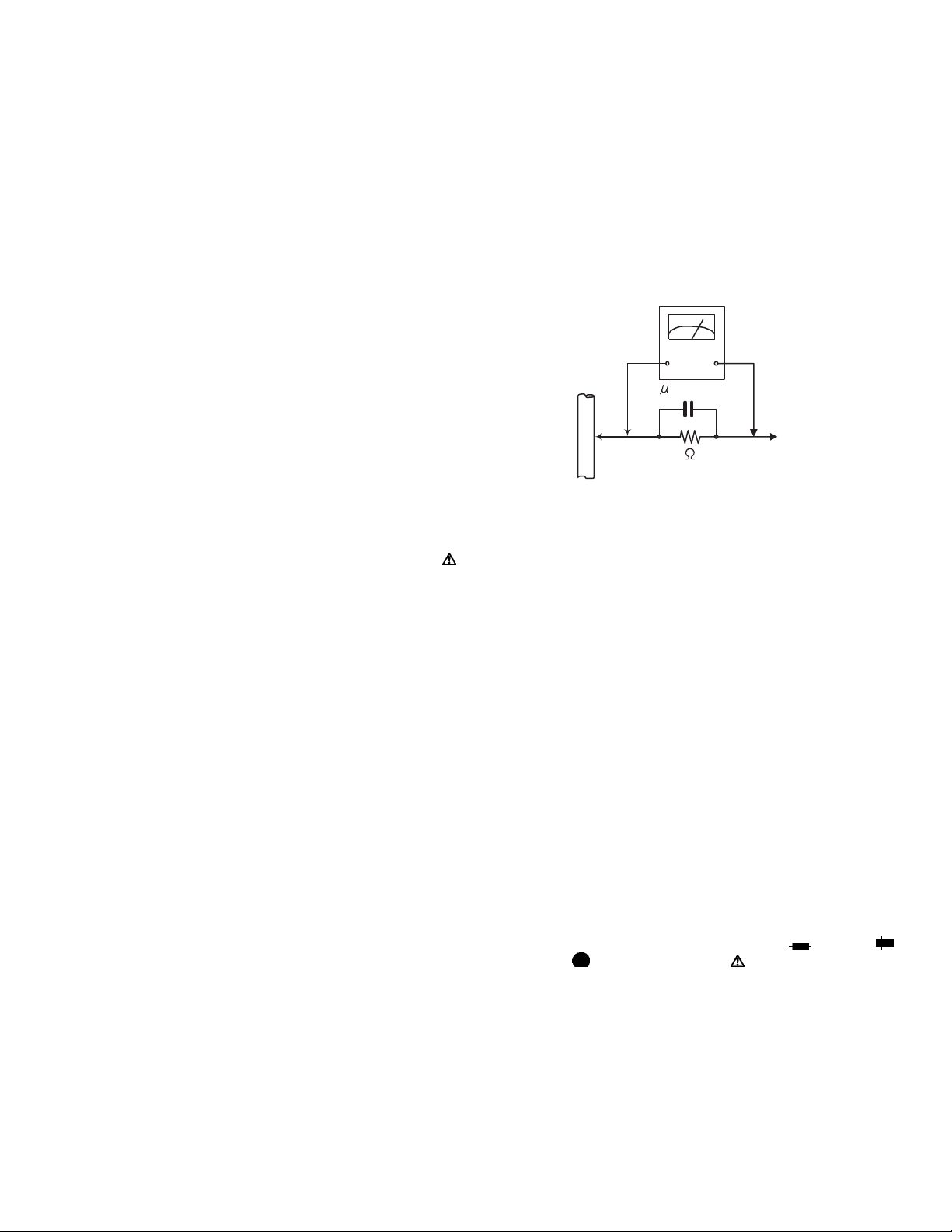
(5) Leakage shock hazard testing
After reassembling the product, always perform an isolation check on the exposed metal parts of the product (antenna terminals, knobs, metal cabinet, screw heads,
headphone jack, control shafts, etc.) to be sure the product
is safe to operate without danger of electrical shock.Do not
use a line isolation transformer during this check.
• Plug the AC line cord directly into the AC outlet. Using a
"Leakage Current Tester", measure the leakage current
from each exposed metal parts of the cabinet, particularly any exposed metal part having a return path to the
chassis, to a known good earth ground. Any leakage current must not exceed 0.5mA AC (r.m.s.).
• Alternate check method
Plug the AC line cord directly into the AC outlet. Use an
AC voltmeter having, 1,000Ω per volt or more sensitivity
in the following manner. Connect a 1,500Ω 10W resistor
paralleled by a 0.15µF AC-type capacitor between an ex-
posed metal part and a known good earth ground.
Measure the AC voltage across the resistor with the AC
voltmeter.
Move the resistor connection to each exposed metal
part, particularly any exposed metal part having a return
path to the chassis, and measure the AC voltage across
the resistor. Now, reverse the plug in the AC outlet and
repeat each measurement. Voltage measured any must
not exceed 0.75 V AC (r.m.s.). This corresponds to 0.5
mA AC (r.m.s.).
AC VOLTMETER
(Having 1000
ohms/volts,
or more sensitivity)
0.15 F AC TYPE
Place this
probe on
1500 10W
Good earth ground
1.2 Warning
(1) This equipment has been designed and manufactured to
meet international safety standards.
(2) It is the legal responsibility of the repairer to ensure that
these safety standards are maintained.
(3) Repairs must be made in accordance with the relevant
safety standards.
(4) It is essential that safety critical components are replaced
by approved parts.
(5) If mains voltage selector is provided, check setting for local
voltage.
1.3 Caution
Burrs formed during molding may be left over on some parts
of the chassis.
Therefore, pay attention to such burrs in the case of preforming repair of this system.
1.4 Critical parts for safety
In regard with component parts appearing on the silk-screen
printed side (parts side) of the PWB diagrams, the parts that are
printed over with black such as the resistor ( ), diode ( )
and ICP ( ) or identified by the " " mark nearby are critical
for safety. When replacing them, be sure to use the parts of the
same type and rating as specified by the manufacturer.
(This regulation dose not Except the J and C version)
each exposed
metal part.
(No.MB376)1-3
Page 4
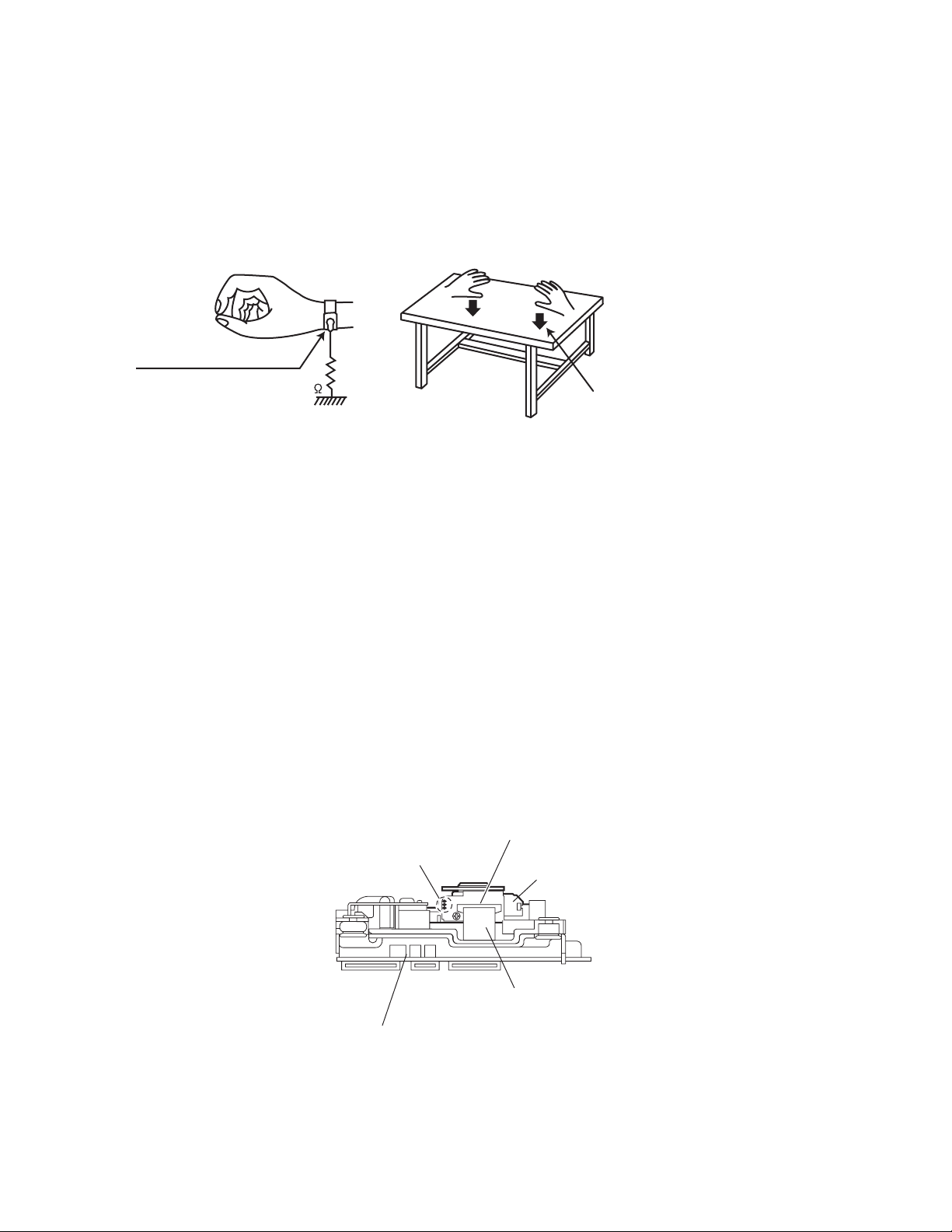
1.5 Preventing static electricity
Electrostatic discharge (ESD), which occurs when static electricity stored in the body, fabric, etc. is discharged, can destroy the laser
diode in the traverse unit (optical pickup). Take care to prevent this when performing repairs.
1.5.1 Grounding to prevent damage by static electricity
Static electricity in the work area can destroy the optical pickup (laser diode) in devices such as laser products.
Be careful to use proper grounding in the area where repairs are being performed.
(1) Ground the workbench
Ground the workbench by laying conductive material (such as a conductive sheet) or an iron plate over it before placing the
traverse unit (optical pickup) on it.
(2) Ground yourself
Use an anti-static wrist strap to release any static electricity built up in your body.
(caption)
Anti-static wrist strap
1M
Conductive material
(conductive sheet) or iron palate
(3) Handling the optical pickup
• In order to maintain quality during transport and before installation, both sides of the laser diode on the replacement optical
pickup are shorted. After replacement, return the shorted parts to their original condition.
(Refer to the text.)
• Do not use a tester to check the condition of the laser diode in the optical pickup. The tester's internal power source can easily
destroy the laser diode.
1.6 Handling the traverse unit (optical pickup)
(1) Do not subject the traverse unit (optical pickup) to strong shocks, as it is a sensitive, complex unit.
(2) Cut off the shorted part of the flexible cable using nippers, etc. after replacing the optical pickup. For specific details, refer to the
replacement procedure in the text. Remove the anti-static pin when replacing the traverse unit. Be careful not to take too long a
time when attaching it to the connector.
(3) Handle the flexible cable carefully as it may break when subjected to strong force.
(4) I t is not possible to adjust the semi-fixed resistor that adjusts the laser power. Do not turn it.
1.7 Attention when traverse unit is decomposed
*Please refer to "Disassembly method" in the text for the pickup unit.
• Apply solder to the short land sections before the flexible wire is disconnected from the connecto on the servo board. (If the flexible
wire is disconnected without applying solder, the pickup may be destroyed by static electricity.)
• In the assembly, be sure to remove solder from the short land sections after connecting the flexible wire.
Connector
Short land section
Pickup
1-4 (No.MB376)
Card wire
Traverse mechanism assembly
Page 5

SECTION 2
SPECIFIC SERVICE INSTRUCTIONS
This service manual does not describe SPECIFIC SERVICE INSTRUCTIONS.
(No.MB376)1-5
Page 6
SECTION 3
DISASSEMBLY
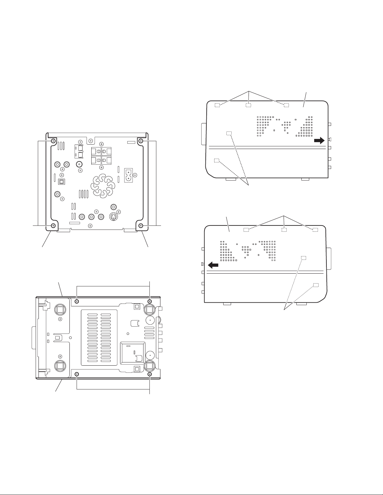
3.1 Main body section
3.1.1 Removing the side panel L and side panel R
(See Figs.1 to 4)
(1) From the back side of the main body, remove the four
screws A attaching the side panels L/R. (See Fig.1.)
(2) From the bottom side of the main body, remove the four
screws B attaching the side panels L/R. (See Fig.2.)
(3) From the both sides of the main body, release the joint a in
the direction of the arrow and remove the side panels L/R
toward this side. (See Figs.3 and 4.)
a
a
Fig.3
Side panel R
A A
Side panel R Side panel L
Fig.1
Side panel R
B
Side panel L
a
a
Fig.4
Side panel L
1-6 (No.MB376)
B
Fig.2
Page 7
3.1.2 Removing the top panel assembly
(See Figs.5 to 6)
• Remove the side panels L/R.
(1) From the front side of the main body, pull out the volume
knob assembly in the direction of the arrow. (See Fig.5.)
(2) Remove the two screws C and remove the volume orna-
ment. (See Fig.5.)
(3) From the both sides of the main body, remove the two
screws D, two screws E and screw F. (See Figs.5 and 6)
Reference:
When attaching the screw F, attach the earth wire with it.
(See Fig.6.)
(4) Remove the screw G attaching the top panel assembly.
(See Fig.6.)
(5) Release the joints b and remove the joints c in the direction
of the arrow. (See Figs.5 and 6.)
(6) Disconnect the card wire from the connector CN427
micom board while lifting the top panel assembly. (See
Fig.5.)
on the
Volume knob assembly
D
c
C
C
Volume ornament
Top panel assembly
CN427
Fig.5
E
Micom board
b
Top panel assembly
G
E
b
Top panel assembly
Earth wire
F
Fig.6
D
c
(No.MB376)1-7
Page 8
3.1.3 Removing the front panel assembly
(See Figs.7 to 9)
• Remove the side panels L/R and top panel assembly.
(1) From the bottom side of the main body, remove the two
screws H attaching the front panel assembly. (See Fig.7.)
(2) From the forward side of the micom board, disconnect the
card wire from the connector CN426
(3) Disconnect the wire from the connector CN501 on the mi-
com board. (See Fig.8.)
(4) From the right side of the main body, remove the screw J
and remove the earth wire. (See Fig.8.)
Reference:
• When attaching the screw J, attach the earth wire with
it. (See Fig.8.)
• After attaching the earth wire, fix it with the spacer as
before. (See Fig.8.)
(5) From the bottom and both sides of the main body, release
the joints (d, e) of the front panel assembly and remove the
front panel assembly in the direction of the arrow. (See
Figs.7 to 9.)
. (See Fig.8.)
Front panel assembly
CN501
CN426
Micom board
Front panel assembly
H
H
Fig.7
d
e
Front panel assembly
Spacer
Fig.8
Earth wire
e
J
1-8 (No.MB376)
Fig.9
Page 9
3.1.4 Removing the tuner
(See Figs.10 and 11)
• Remove the side panels L/R and top panel assembly.
(1) From the back side of the main body, remove the two
screws K attaching the tuner to the rear panel. (See
Fig.10.)
(2) Disconnect the card wire from the connector CN1
tuner. (See Fig.11.)
on the
K
Tuner
K
Fig.10
CN1
Tuner
Fig.11
(No.MB376)1-9
Page 10
3.1.5 Removing the rear panel
(See Fig.12)
• Remove the side panels L/R and top panel assembly.
(1) From the back side of the main body, remove the ten
screws M and screw N attaching the rear panel.
(2) From the both sides of the main body, release the joints f
and remove the rear panel.
M
Rear panel
N
M
ff
M
Fig.12
1-10 (No.MB376)
Page 11
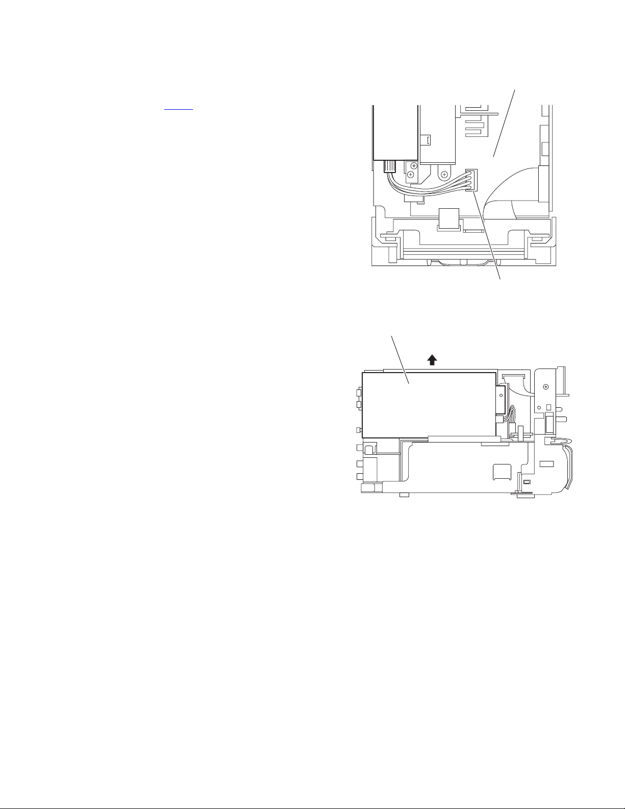
3.1.6 Removing the switching power supply
(See Figs.13 and 14)
• Remove the side panels L/R, top panel assembly and rear
panel.
(1) From the top side of the main body, disconnect the wires
from the connector CN200
Fig.13.)
(2) Take out the switching power supply in the direction of the
arrow. (See Fig.14.)
on the regulator board. (See
Regulator board
CN200
Fig.13
Switching power supply
Fig.14
(No.MB376)1-11
Page 12
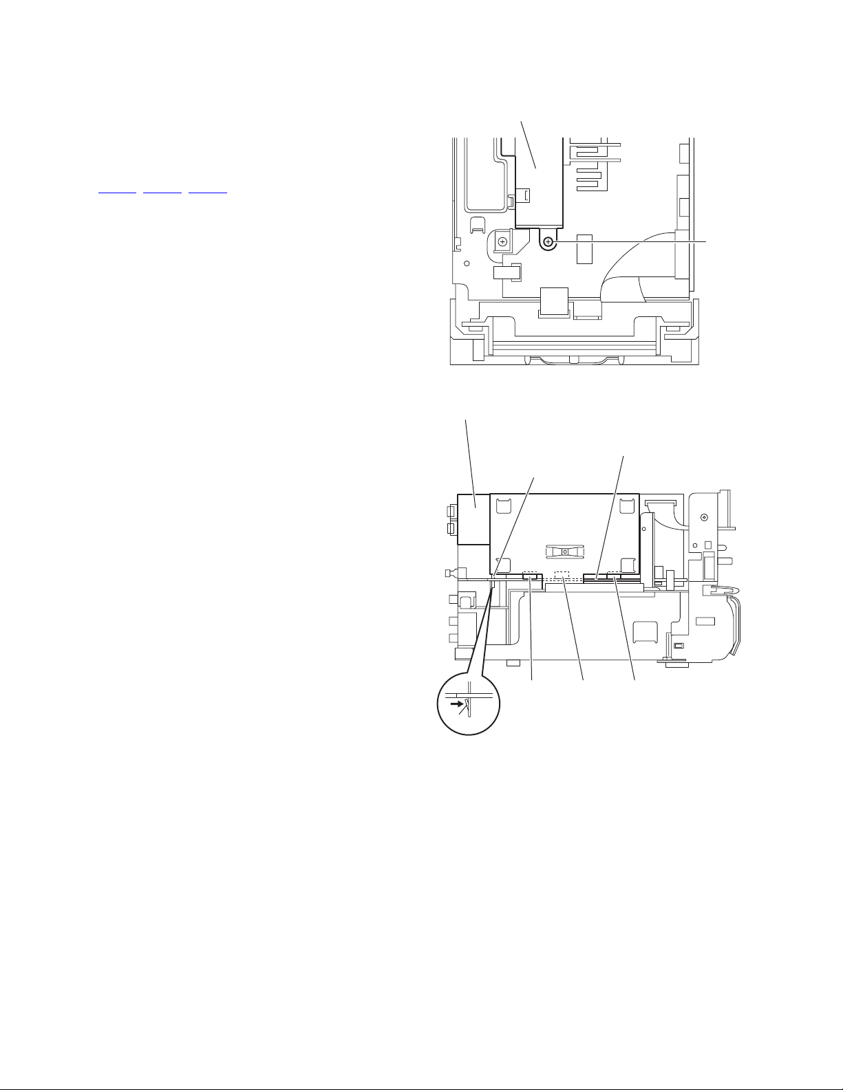
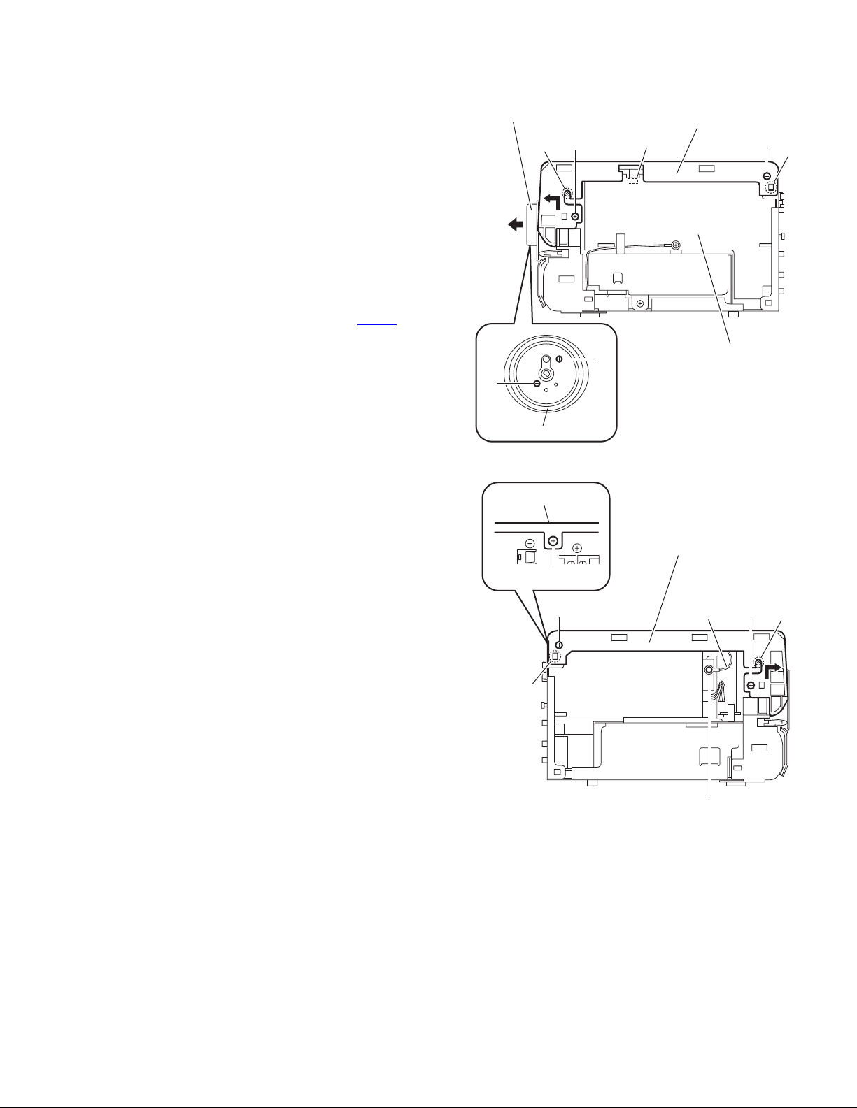
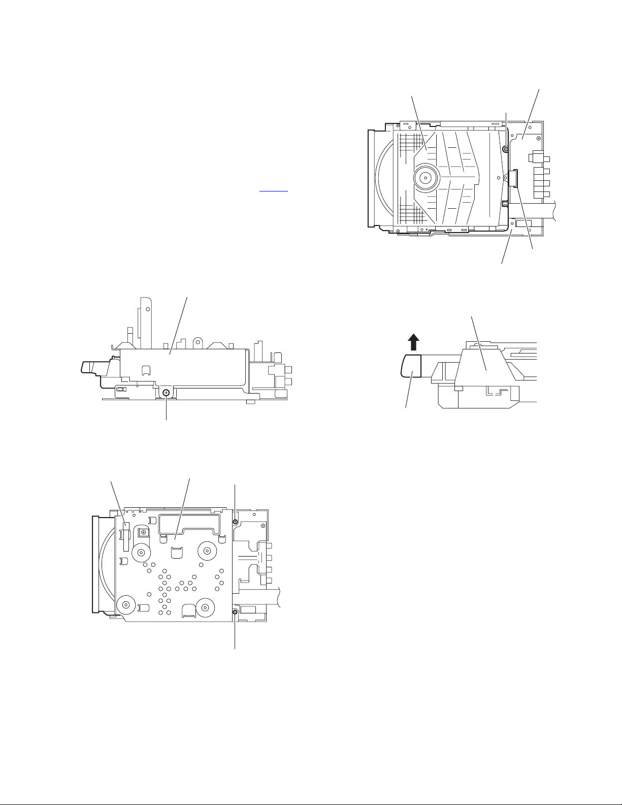
3.1.7 Removing the digital amplifier board assembly
(See Figs.15 and 16)
• Remove the side panels L/R, top panel assembly, rear panel
and switching power supply.
(1) From the top side of the main body, remove the screw P
attaching the digital amplifier board assembly. (See
Fig.15.)
(2) From the left side of the main body, disconnect the connec-
tors (CN310
assembly from the regulator board. (See Fig.16.)
(3) Release the joint g of the shield case B in the direction of
the arrow and take out the digital amplifier board assembly
from the main body. (See Fig.16.)
, CN311, CN312) on the digital amplifier board
Digital amplifier board assembly
P
Fig.15
Digital amplifier board assembly
Regulator board
Shield case B
1-12 (No.MB376)
CN312 CN311 CN310
g
Fig.16
Page 13
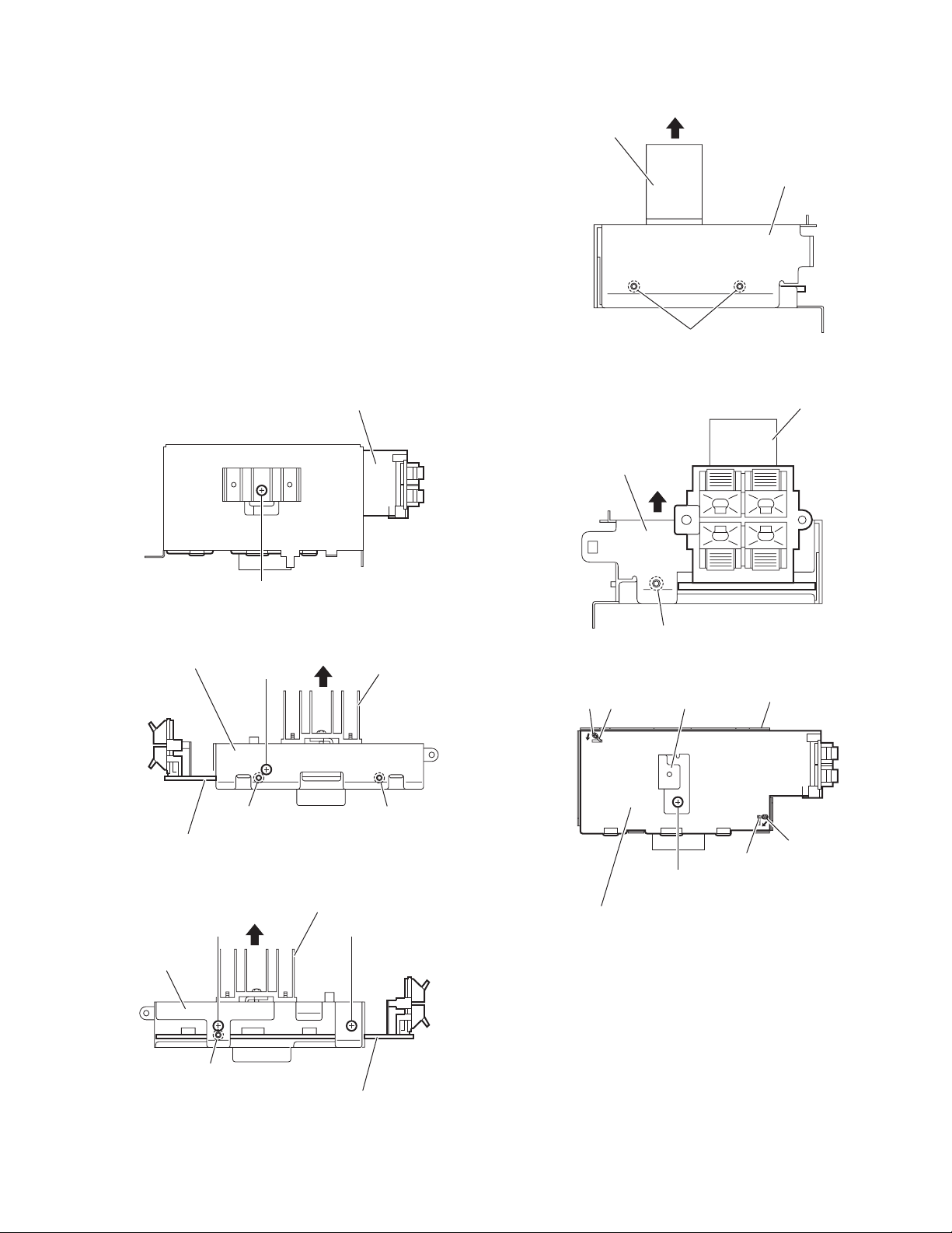
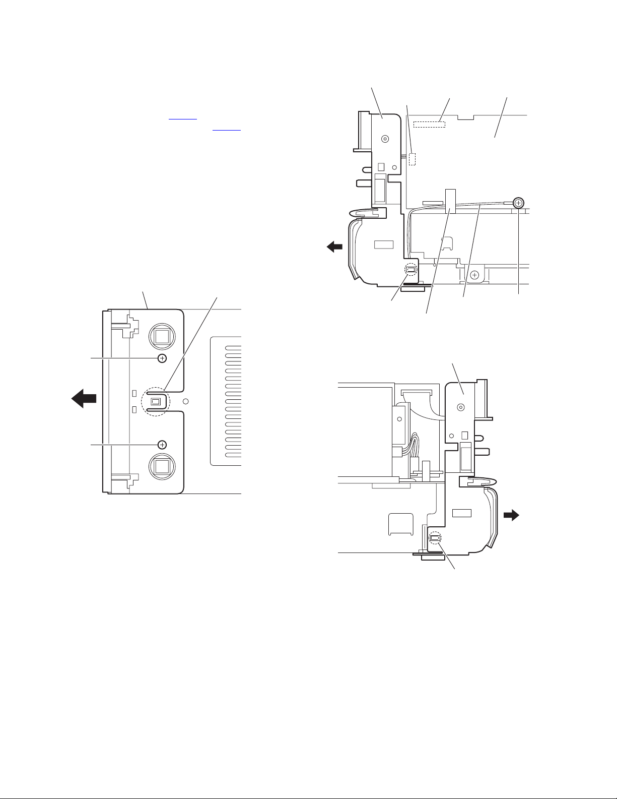
3.1.8 Removing the digital amplifier board
(See Figs.17 to 22)
• Remove the side panels L/R, top panel assembly, rear panel,
switching power supply and digital amplifier board assembly.
(1) From the forward side of the digital amplifier board assem-
bly, remove the screw Q. (See Fig.17.)
(2) From the top and bottom sides of the digital amplifier board
assembly, remove the three screws R. (See Figs.18 and
19.)
(3) Release the joints (h, j, k, m) and remove the shield case
B with the heat sink in the direction of the arrow. (See
Figs.18 to 21.)
(4) From the forward side of the digital amplifier board, remove
the screw R attaching the heat sink. (See Fig.22.)
(5) Remove the solders from the soldered sections (n, p) and
bend the sections (q, r) of the shield case A in the direction
of the arrow. (See Fig.22.)
(6) Take out the digital amplifier board from the shield case A.
Heat sink
Shield case B
k
Fig.20
Digital amplifier board assembly
Q
Fig.17
Shield case B
Digital amplifier board assembly
Shield case B
R
hh
Fig.18
Heat sink
Heat sink
RR
Shield case B
m
Fig.21
q
n
Heat sink
R
Digital amplifier board
Fig.22
Heat sink
Shield case A
p
r
j
Digital amplifier board assembly
Fig.19
(No.MB376)1-13
Page 14
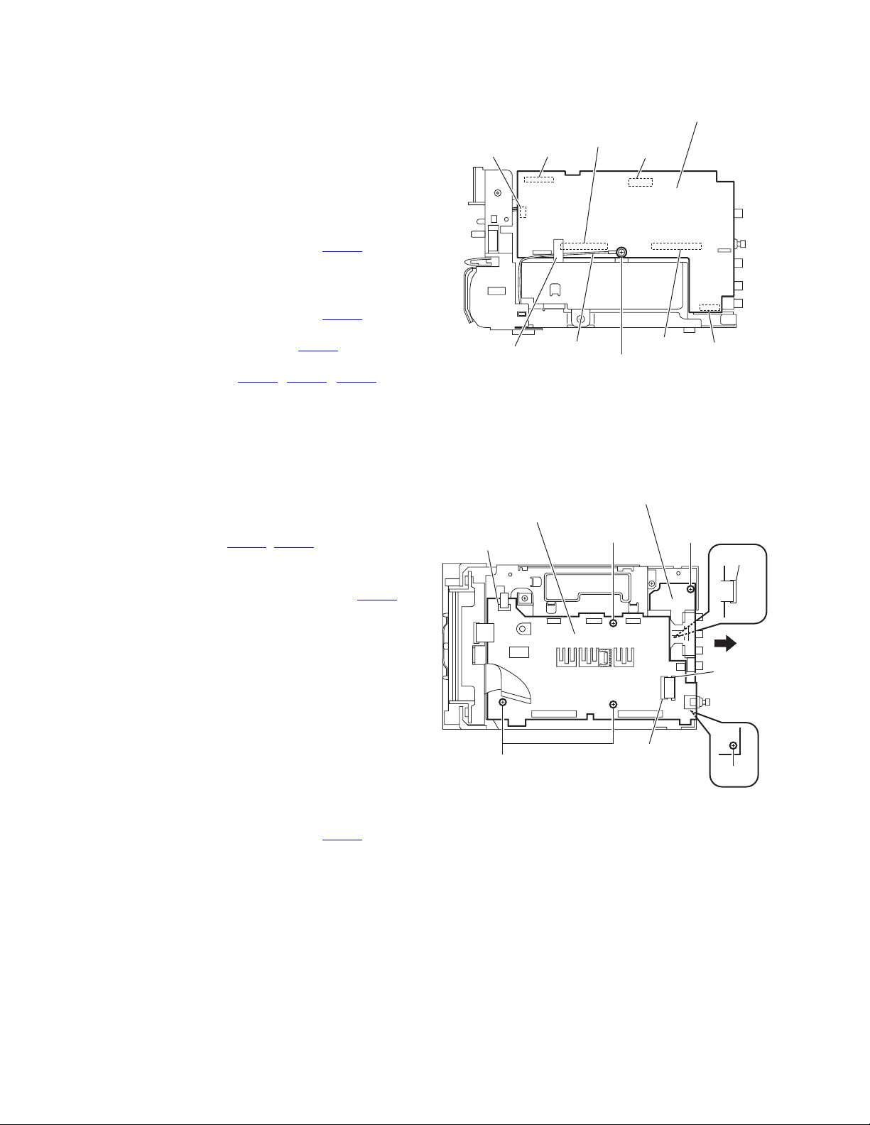
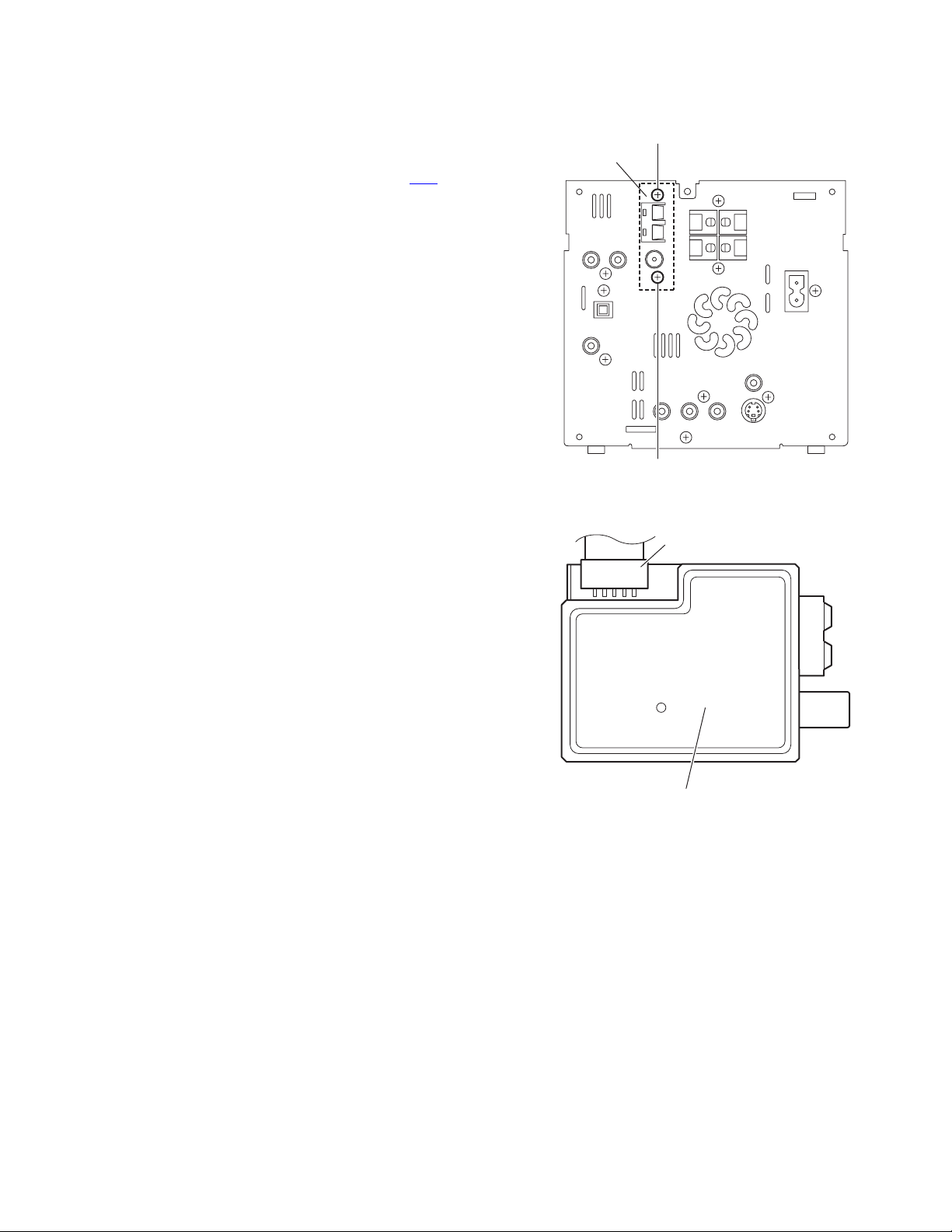
3.1.9 Removing the micom board
(See Fig.23)
• Remove the side panels L/R, top panel assembly and rear
panel.
(1) From the right side of the main body, remove the screw S
attaching the micom board.
Reference:
• When attaching the screw S, attach the earth wire with
it.
• After attaching the earth wire, fix it with the spacer as
before.
(2) Disconnect the card wire from the connector CN421
forward side of the micom board.
Reference:
Remove the tuner as required. (See Figs.10 and 11.)
(3) Disconnect the card wire from the connector CN426
forward side of the micom board.
(4) Disconnect the wire from the connector CN501
ward side of the micom board.
(5) Disconnect the connectors (CN423
the micom board from the regulator board toward this side
to remove the micom board.
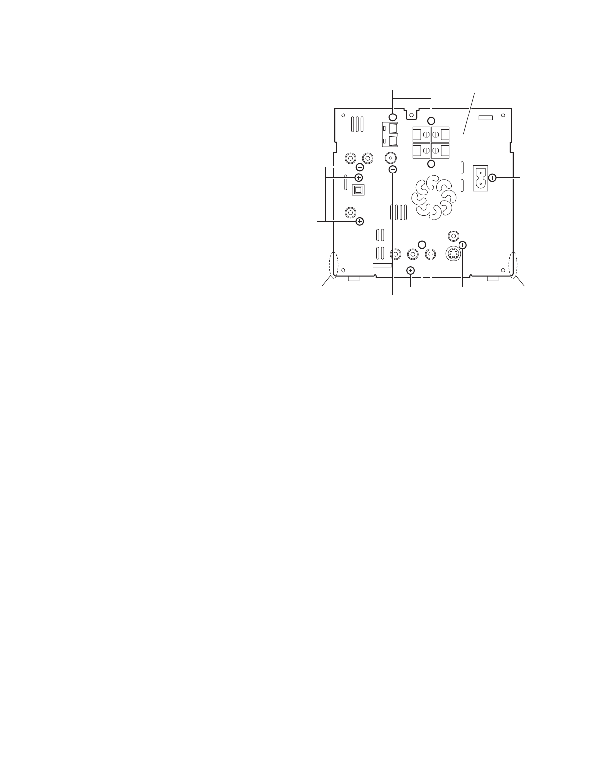
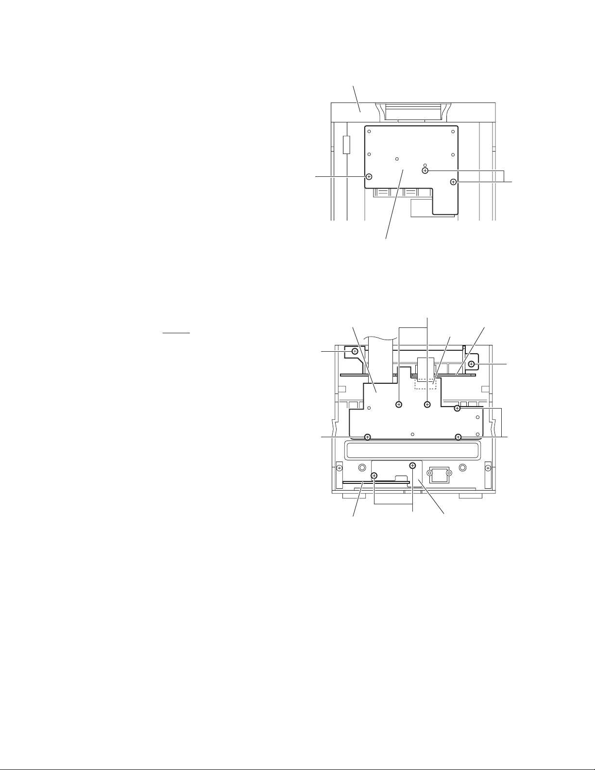
3.1.10 Removing the regulator board
(See Fig.24)
• Remove the side panels L/R, top panel assembly, tuner, rear
panel, switching power supply, digital amplifier board assembly and micom board.
(1) From the top side of the main body, disconnect the card
wires from the connectors (CN208
tor board.
Reference:
When connecting the card wire to the connector CN208
pass it through the hole s of the regulator board as before.
(2) Remove the three screws T and take out the regulator
board.
3.1.11 Removing the video board
(See Fig.24)
• Remove the side panels L/R, top panel assembly, tuner, rear
panel, switching power supply, digital amplifier board assembly and micom board.
Reference:
Remove the regulator board as required.
(1) From the top side of the main body, remove the two screws
U and take out the video board in the direction of the arrow.
(2) Disconnect the card wire from the connector CN703
video board.
, CN424, CN425) on
, CN210) on the regula-
on the
on the
on the for-
on the
Micom board
CN501
Spacer
CN426
CN424
Earth wire
CN421
CN423
CN425
S
Fig.23
Video board
Regulator board
CN210
,
T
CN208
T
Fig.24
U
CN703
s
U
1-14 (No.MB376)
Page 15
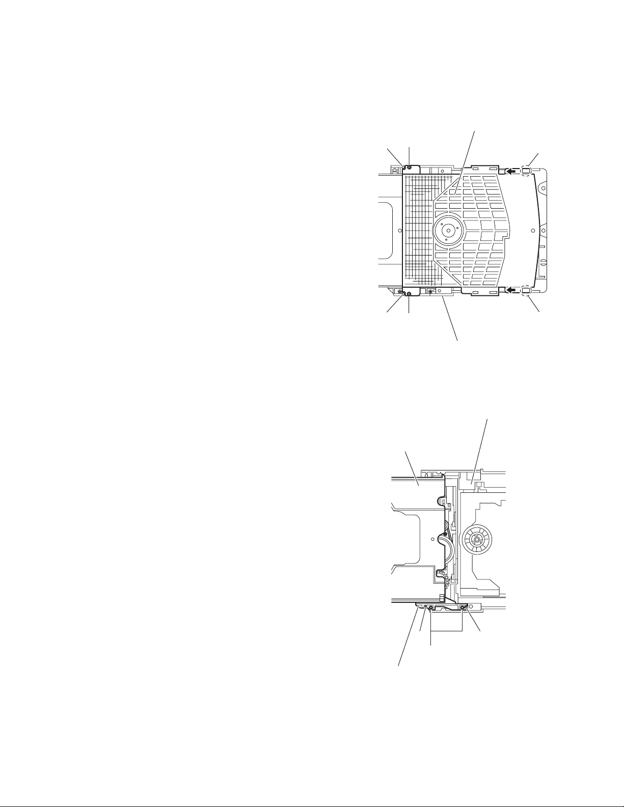
3.1.12 Removing the DVD mechanism assembly
(See Figs.25 to 28)
• Remove the side panels L/R, top panel assembly, tuner, rear
panel, switching power supply, digital amplifier board assembly, micom board and regulator board.
(1) From the right side of the main body, remove the screw V
attaching the metal chassis. (See Fig.25.)
(2) From the top side of the main body, remove the two screws
W and take out the metal chassis. (See Fig.26.)
Reference:
When attaching the metal chassis, pass the card wire
through the hole t on the metal chassis as before.
(3) Disconnect the card wire from the connector CN703
video board. (See Fig.27.)
(4) Remove the screw X and take out the DVD mechanism as-
sembly from the bottom chassis. (See Fig.27.)
Reference:
When the resolution of DVD mechanism assembly is done sequentially, remove a CD fitting in the direction of the arrow.
(See Fig.28.)
on the
DVD mechanism assembly
Bottom chassis
Video board
X
CN703
Metal chassis
CD fitting
V
Fig.25
t
Metal chassis
W
Fig.27
DVD mechanism assembly
Fig.28
Fig.26
W
(No.MB376)1-15
Page 16
3.1.13 Removing the switch board
Y
Y
(See Fig.29)
• Remove the side panels L/R and top panel assembly.
From the inside of the top panel assembly, remove the three
screws Y and take out the switch board.
3.1.14 Removing the front board
(See Fig.30)
• Remove the side panels L/R, top panel and front panel assem-
blies.
(1) From the inside of the front panel assembly, disconnect the
card wire from the connector CN605
(2) Remove the five screws Z and take out the front board.
3.1.15 Removing the FL board
(See Fig.30)
• Remove the side panels L/R, top panel assembly, front panel
assembly and front board.
Remove the two screws Z and take out the FL board.
on the front board.
Top panel assembly
Switch board
Front board
Z
Fig.29
Z
FL board
CN605
Z
3.1.16 Removing the headphone board
(See Fig.30)
• Remove the side panels L/R, top panel and front panel assem-
blies.
(1) Remove the two screws Z and take out the support board.
(2) Take out the headphone board.
Z
Headphone board
Z
Fig.30
Z
Support board
1-16 (No.MB376)
Page 17
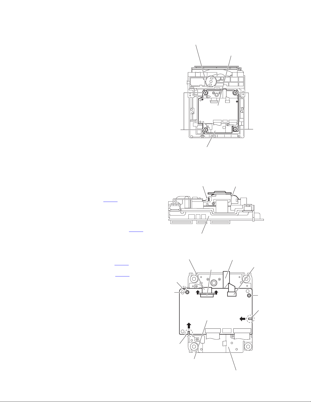
3.2 DVD mechanism section
• Remove the DVD mechanism assembly from the main body.
(See "3.1.6 Removing the DVD mechanism assembly".)
3.2.1 Removing the clamper base
(See Fig.1)
(1) From the top side of the DVD mechanism assembly, re-
move the two screws A attaching the clamper base.
(2) Lift the clamper base in an upward direction to remove it
from the projections a of the DVD mechanism assembly.
(3) Slide the clamper base in the direction of the arrow and re-
move it from the joints b.
Clamper base
A
a
b
3.2.2 Removing the tray assembly
(See Fig.2)
(1) From the top side of the DVD mechanism assembly, re-
move the two screws B attaching the shaft guide of the tray
assembly.
(2) Remove the tray assembly from the projections c of the
DVD mechanism assembly and take out the tray assembly.
a
A
DVD mechanism assembly
Tray assembly
b
Fig.1
DVD mechanism assembly
Shaft guide
cc
B
Fig.2
(No.MB376)1-17
Page 18
3.2.3 Removing the traverse mechanism assembly
(See Figs.3)
(1) From the bottom side of the DVD mechanism assembly, re-
move the four screws C attaching the traverse mechanism
assembly.
(2) Take out the traverse mechanism assembly with the DVD
module board.
DVD mechanism assembly
DVD module board
3.2.4 Removing the DVD module board
(See Figs.4 and 5)
• Remove the traverse mechanism assembly.
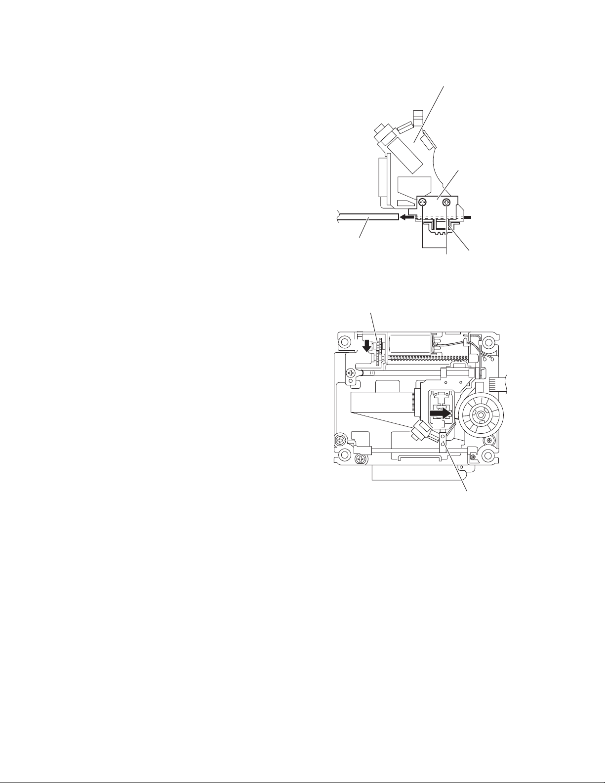
(1) From the side of the traverse mechanism assembly, solder
the short land sections d on the pickup. (See Fig.4.)
(2) From the bottom side of the traverse mechanism assem-
bly, release the lock of the connector CN101
module board in the direction of the arrow 1 and disconnect
the card wire. (See Fig.5.)
Caution:
• Solder the short land sections d on the pickup before
disconnecting the card wire from the connector CN101
on the DVD module board. If the card wire is disconnected without attaching solder, the pickup may be destroyed by static electricity. (See Figs.4 and 5.)
• When attaching the DVD module board, be sure to remove solders from the short land sections d after connecting the card wire to the connector CN101
DVD module board. (See Figs.4 and 5.)
(3) Disconnect the card wire from the connector CN201
DVD module board. (See Fig.5.)
(4) Remove the two screws D attaching the DVD module
board. (See Fig.5.)
(5) Remove the DVD module board from the projection e in an
upward direction and remove the engagement section g in
the direction 3 while removing the engagement section f in
the direction of the arrow 2. (See Fig.5.)
on the DVD
on the
on the
C
Traverse mechanism assembly
Fig.3
d
Traverse mechanism assembly
Fig.4
e
D
Card wire
11
2
Card wire
CN101
C
Pickup
CN201
D
g
3
1-18 (No.MB376)
f
DVD module board
Traverse mechanism assembly
Fig.5
Page 19
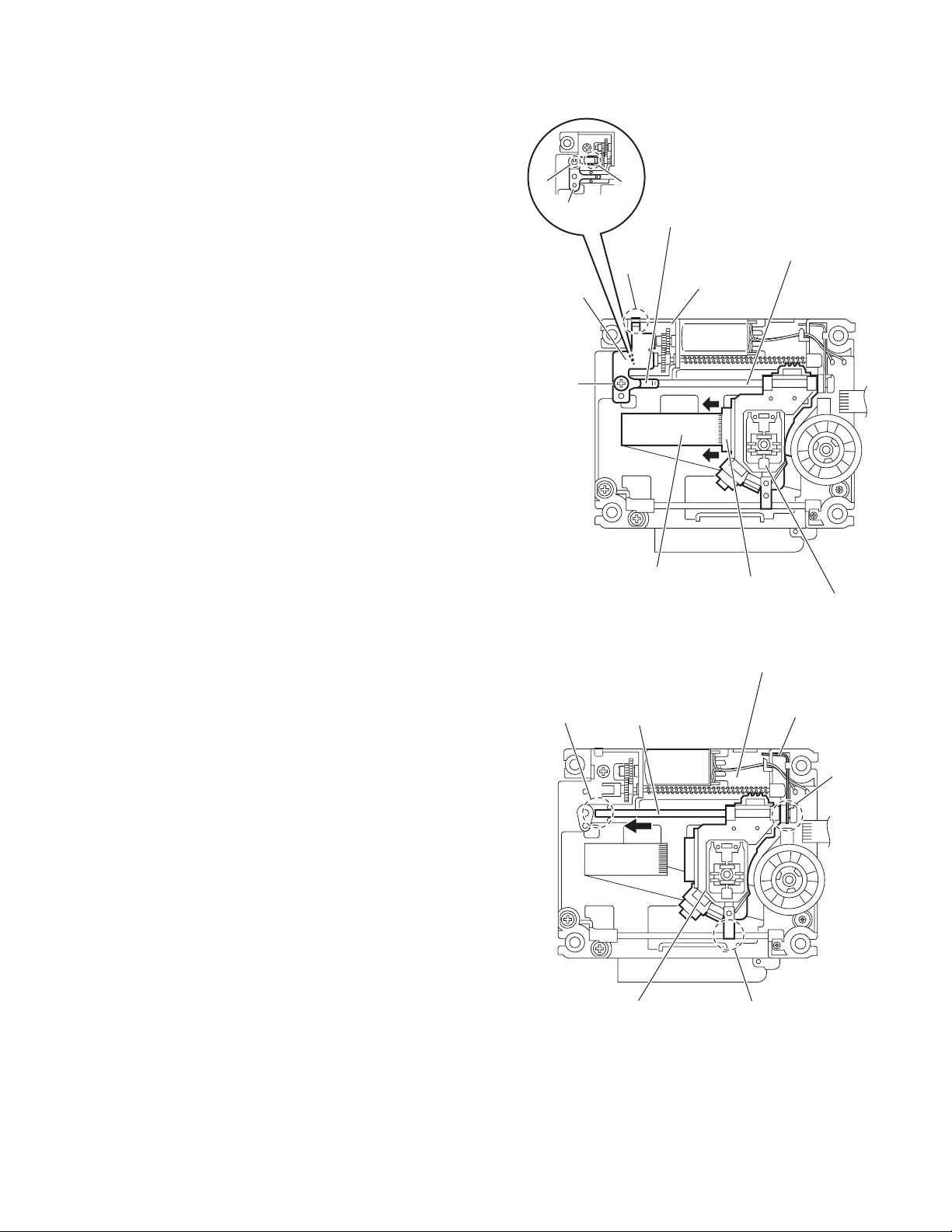
3.2.5 Removing the pickup
(See Figs.4,6 to 8)
• Remove the traverse mechanism assembly.
(1) From the side of the traverse mechanism assembly, solder
the short land sections d on the pickup. (See Fig.4.)
(2) Release the lock of the connector on the pickup in the di-
rection of the arrow and disconnect the card wire. (See
Fig.6.)
Caution:
• Solder the short land sections d on the pickup before
disconnecting the card wire from the connector on the
pickup. If the card wire is disconnected without attaching solder, the pickup may be destroyed by static electricity. (See Figs.4 and 6.)
• When attaching the pickup, be sure to remove solders
from the short land sections d after connecting the
card wire to the connector on the pickup. (See Figs.4
and 6.)
(3) Remove the screw E attaching the plate and thrust spring.
(See Fig.6.)
(4) Remove the engagement section h attaching the plate to
the feed holder and remove the plate. (See Fig.6.)
(5) Remove the engagement sections (i, j), remove the thrust
spring. (See Fig.6.)
(6) Remove the shaft of the pickup from the section k on the
traverse mechanism assembly and remove the shaft from
the section m while moving it in the direction of the arrow.
(See Fig.7.)
(7) Remove the pickup from the section n of the traverse
mechanism assembly and take out the pickup with the
shaft. (See fig.7.)
(8) From the bottom side of the pickup, remove the two screws
F attaching the SW actuator and lead spring. (See Fig.8.)
(9) Pull the shaft out of the pickup. (See Fig.8.)
i
Thrust spring
Plate
E
j
Thrust spring
h
Card wire
Traverse mechanism assembly
Feed holder
Connector
Fig.6
Traverse mechanism assembly
Pickup
k
Shaft
Pickup
Fig.7
Torsion spring
m
n
(No.MB376)1-19
Page 20
3.2.6 Attaching the pickup
(See Figs.4,6 to 9)
• See "3.2.5 Removing the pickup".
(1) Attach the shaft, SW actuator and lead spring to the pickup.
(See Fig.8.)
(2) Align the pickup to the section n of the traverse mechanism
assembly first and set the both ends of the shaft of the pickup in the sections (k, m) of the traverse mechanism assembly. (See Fig.7.)
Note:
When attaching the shaft to the section m, attach it under
the torsion spring. (See Fig.7.)
(3) Attach the plate and thrust spring. (See Fig.6.)
(4) Remove solders from the short land sections d after con-
necting the card wire to the connector on the pickup. (See
Figs.4 and 6.)
(5) Turn the feed gear M in the direction of the arrow 1 to move
the pickup in the direction of the arrow 2. (See Fig.9.)
Shaft
Feed gear M
Fig.8
Pickup
SW actuator
Lead spring
F
1
2
Pickup
Fig.9
1-20 (No.MB376)
Page 21

3.2.7 Removing the feed motor
(See Figs.10 to 12)
• Remove the traverse mechanism assembly.
(1) From the top side of the traverse mechanism assembly, re-
move the screw G attaching the plate and thrust spring.
(See Fig.10.)
(2) Remove the engagement section p attaching the plate to
the feed holder and remove the plate. (See Fig.10.)
(3) Remove the engagement sections (q, r), remove the thrust
spring. (See Fig.10.)
(4) Remove the wires from the soldered section s on the spin-
dle motor board. (See Fig.11.)
Reference:
When attaching the feed motor, pass the wire through
the section t on the spindle base. (See Fig.11.)
(5) Remove the feed holder, feed motor, lead screw, feed gear
E and feed gear M at the same time after removing the
three screws H attaching the feed holder. (See Fig.11.)
(6) From the side of the feed holder, remove the two screws J
attaching the feed motor. (See Fig.12.)
3.2.8 Removing the spindle motor board
(See Figs.11 and 13)
• Remove the traverse mechanism assembly and DVD module
board.
(1) From the top side of the traverse mechanism assembly, re-
move the wires from the soldered section s on the spindle
motor board. (See Fig.11.)
(2) From the bottom side of the traverse mechanism assem-
bly, remove the three screws K attaching the spindle motor
board. (See Fig.13.)
Feed gear M
Feed gear E
H
Feed holder
J
H
Feed motor
Spindle base
Fig.11
Lead screw
Wires
Spindle motor board
Feed holder
t
s
q
Thrust spring
Plate
G
r
Thrust spring
p
Fig.12
Traverse mechanism assembly
Feed holder
Traverse mechanism assembly
K
Fig.13
Fig.10
(No.MB376)1-21
Page 22

3.2.9 Removing the switch board
(See Fig.14.)
(1) From the bottom side of the DVD mechanism assembly, re-
move the screw L attaching the switch board.
(2) Disconnect the card wire from the connector CN1 on the
switch board.
(3) Remove the wires from the soldered section u on the
switch board.
(4) Lift the switch board while pressing the claw v of the DVD
mechanism assembly in the direction of the arrow and remove it from the section w.
Reference:
Put the wires on the section x after attaching the switch board
to the DVD mechanism assembly.
3.2.10 Removing the motor
(See Figs.14 and 15)
• Remove the clamper base and tray assembly.
(1) From the bottom side of the DVD mechanism assembly, re-
move the wires from the soldered section u on the switch
board. (See Fig.14.)
(2) From the top side of the DVD mechanism assembly, re-
move the belt from the motor pulley. (See Fig.15.)
Note:
Take care not to attach grease on the belt.
(3) Remove the two screws M attaching the motor to the DVD
mechanism assembly and take out the motor from the bottom side of the DVD mechanism assembly. (See Fig.15.)
Reference:
Put the wires on the section x after attaching the motor to the
DVD mechanism assembly. (See Fig.14.)
Card wire
L
M
Switch board
CN1
w
x
u
v
Wires
DVD mechanism assembly
Fig.14
Motor pulley
Belt
DVD mechanism assembly
Fig.15
1-22 (No.MB376)
Page 23

4.1 Service mode
4.1.1 Confirming contents
(1) Tuner AM switch to 9kHz-step
(2) Tuner AM switch to 10kHz-step
(3) Cold start
(4) Tray lock
(5) DVD test mode
(6) DVD initialize
4.1.2 Confirming methods
SECTION 4
ADJUSTMENT
1. Tuner AM switch to 9kHz-step
AM frequency change to 9kHz at U & A-version.
Press the [
main unit and set the tuner in AM mode
Press the [
the main unit to enter in standby mode
Press the [
the
[DOWN ] button on the main unit.
AM frequency is set to 9kHz-step.
2. Tuner AM switch to 10kHz-step
AM frequency change to 10kHz at U & A-version.
Press the [
main unit and set the tuner in AM mode
Press the [
the main unit to enter in standby mode
STANDBY/ON]
STANDBY/ON]
STANDBY/ON] button while pressing
FL indication
" AM 9KHZ "
STANDBY/ON]
STANDBY/ON]
button on the
.
button again on
.
button on the
.
button again on
.
3. Cold start
Cold start processing.
Press the [
[STOP] and [0] keys on the remote controller
simultaneously
4. Tray lock
Loader-mecha is locked.
EJECT processing isn't done by pushing EJECT key
at tray lock on state.
Then display to LOCKED / UNLOCKED.
EJECT is pushed, pushing STOP again, tray lock is off.
Back up to tray locked ON/OFF.
Press the [
[STOP] button on the main unit in standby mode.
AUDIO
Cold start is completed.
EJECT] button while pressing the
] key
at standby.
FL indication
" COLD "
FL indication
" LOCKED "
while pressing the
Press the [
the
STANDBY/ON] button while pressing
[ UP] button on the main unit.
FL indication
" AM 10KHZ "
AM frequency is set to 10kHz-step.
Press the [
button again on the main unit in standby mode.
Press the [
button again on the main unit in standby mode.
EJECT] button while pressing the
FL indication
" UNLOCKED "
EJECT] button while pressing the
[STOP]
[STOP]
(No.MB376)1-23
Page 24

5. DVD test mode
In to the DVD test mode.
Test mode contents is refer to module specification.
DVD test mode is canceled by POWER OFF and
except source DVD.
Insert a power cord in an outlet while pressing
the [
PLAY]
and [PAUSE] buttons on the main
unit simultaneously
.
6. DVD initialize
DVD module initialized.
LCD segment is light on at initialize command.
DVD test mode.
Press the [
button on the main unit
3D PHONIC]
.
The details refer to "4.1.3 DVD test mode".
4.1.3 DVD test mode
1. To enter DVD TEST mode,
(1) AC POWER ON while holding PLAY+PAUSE keys.
(2) DVD Mecha will start in TEST MODE, FL will display:
T xxy vw
2. To exit DVD TEST mode,
During TEST MODE (except for Device Key write & DVD Region Re-write), press POWER KEY.
To exit TEST mode for Device Key Write & DVD Region Re-write, first AC OFF, then AC ON again to return to
normal state.
3. EEPROM INITIALIZATION
3.1 NORMAL INITIALIZE
(1) During DVD TEST MODE, press STOP key on remote control to start NORMAL EEPROM INITIALIZATION.
(2) FL will display:
T xxy vw
This unit is set to DVD test mode.
Initialization state from DVD UNIT
Study state information from DVD UNIT
Region number
Received DESTINATION information:
JC/1U/D/E/2U/3U/UB/UT/4U/UY/EE/UF
DVD initialize is completed.
3.2 FULL INITIALIZE
(1) During DVD TEST MODE, press >>| key on set 2 seconds control to start FULL EEPROM INITIALIZATION.
(2) FL will display:
4. DEVICE KEY CHECKSUM DISPLAY
(1) During DESTINATION INFO display screen (1), press MENU key to enter DEVICE KEY CHECKSUM display.
(2) FL will display:
1-24 (No.MB376)
Initialization state from DVD UNIT
T xxy vw
Initialization state from DVD UNIT
DKxxxx (Example) DK470B
Page 25

5. DVD check mode
DVD test mode
Press the [
MENU
] key twice
on the remote controller
FL indication
" CHECK "
Press the [1] key on
the remote controller
Press the [2] key on
the remote controller
Press the [3] key on
the remote controller
Press the [4] key on
the remote controller
Press the [5] key on
the remote controller
Press the [6] key on
the remote controller
Press the [7] key on
the remote controller
Press the [8] key on
the remote controller
.
START PLAYBACK
.
Perform SEARCH TNO+1
.
Perform SEARCH TNO-1
.
Light up CD_LD and
display laser current
.
Light up DVD_LD and
display laser current
.
Enter DVD x 2 JITTER
MEASUREMENT MODE
.
View EEPROM (MECHA)
content in -1 address step.
.
View EEPROM (MECHA)
content in +1 address step.
.
FL indication
" PLAYBACK "
FL indication FL indication
"WOBBLE"
(After 2 seconds)
"xxxxyyyy"
FL indication
"CHECK"
FL indication FL indication
"COLD LSR"
FL indication FL indication
"DVDLDLSR"
FL indication FL indication
"JITX1"
FL indication FL indication
"EEP BWD"
FL indication FL indication
"EEP FWD"
(After 2 seconds)
"xxxxyyyy"
(After 2 seconds)
"xxxxyyyy"
(After 2 seconds)
"xxxxyyyy"
(After 2 seconds)
"xxxxyyyy"
(After 2 seconds)
"xxxxyyyy"
Press the [9] key on
the remote controller
Press the [10] key on
the remote controller
A
Perform TEMPERATURE
SENSOR VALUE
.
Perform SEARCH DVD_DL
PARALLEL DISC DESIGNATED
POSITION and JITTER
MEASUREMENT
.
FL indication FL indication
"TEMP"
FL indication FL indication
"DVD-DL"
(After 2 seconds)
"xxxxyyyy"
(After 2 seconds)
"xxxxyyyy"
(No.MB376)1-25
Page 26

A
Press the [0] key on
the remote controller
Press the [
the remote controller
Press the [
+10
PLAY
] key on
.
] key
on the remote controller
Press the [
STOP
] key
on the remote controller
Press the [
MENU
] key
on the remote controller
Return to starting screen
of DVD test mode.
Press the [
STANDBY/ON
button on the main unit
Perform monitor output.
.
Initialize EEPROM (MECHA)
Start PLAYING and obtain
LASER CURRENT and
JITTER value.
.
Stop JITTER measurement.
.
.
]
.
FL indication FL indication
"MONITOR"
(After 2 seconds)
"xxxxyyyy"
FL indication
"INIT"
FL indication FL indication
"LSR JIT"
(After 2 seconds)
"xxxxyyyy"
FL indication
"xxxxyyyy"
DVD check mode is completed.
1-26 (No.MB376)
Page 27

4.2 Indicating check for FL display
4.2.1 FL display (DVD function)
1
DVD
2 OPEN DVD
Other source
3 CLOSE DVD
Other source
4 NO DISC DVD
Other source
5 TOC READING
6 POWER OFF
7 ERROR DISC
REGION CODE ERROR
TRAY LOCK
FL displayFunctionNo.
DVD
OPEN
CLOSE
NO D I SC
READ I NG
SEE YOU
REUG
I
O
L
O
C
N
KCE
Note
Under tray OPEN operation, and OPEN state.
The last source is displayed.
Under tray CLOSE operation.
The last source is displayed.
At the time of DISC-less decision.
The last source is displayed.
Under POWER OFF processing.
Other keys are not received while carrying out this
processing.
0
:
0
When DISC classification is 0x00 or 0x0C.
0
E
R
R
.
D
At the time of TRAY LOCK
TRAY UNLOCK
8 DVD AUDIO
STOP
PLAY
(TOP MENU/MENU)
PLAY
SEARCH
+10 KEY INPUT
GROUP +10 KEY INPUT
N
L
O
K
E
D
D
V
D
A
U
D
I
G
3
D
V
D
D
V
D
D
V
D
T
0
1
D
V
D
T
0
1
D
V
D
T
1
-
D
V
D
G
1
-
D
V
D
S
T
O
P
A
G
3
T
A
M
E
N
U
A
M
E
N
U
1
:
2
3
:
A
G
1
T
-
:
-
-
:
A
G
1
T
1
:
2
3
:
A
G
1
T
1
:
2
3
:
A
-
T
At the time of TRAY LOCK release
O
1
5
4
1
0
-
-
-
1
5
4
-
1
5
4
1
(No.MB376)1-27
Page 28

REPEAT GROUP
REPEAT TRACK
PROGRAM
(NO ENTRY)
PROGRAM (STOP)
PROGRAM (PLAY)
RANDOM (STOP)
RANDOM (SEARCH)
RANDOM
(PLAY/PAUSE)
FL displayFunctionNo.
display of Current condition
display of Current condition
P
R
O
G
R
A
M
P
2
G
2
T
T
1
5
0
:
0
1
:
R
A
N
D
O
M
T
x
x
-
:
-
-
:
T
1
1
:
2
3
:
Note
1
5
2
3
-
-
4
5
RESUME
DOWNMIX PROHIBITED
WATER MARK
9 DVD VIDEO
STOP
PLAY (TITLE/MENU)
PLAY
PAUSE
SEARCH
+10 KEY INPUT
R
E
S
U
M
E
L
R
O
N
L
Y
M
U
L
T
I
C
H
N
O
A
U
D
I
O
T
1
5
D
V
D
D
V
D
D
V
D
C
1
3
D
V
D
C
1
3
D
V
D
C
2
D
V
D
C
1
-
D
V
D
S
T
O
P
UNDER FL DISPLAY MODE
T
1
5
M
E
N
M
E
N
1
:
2
3
T
1
2
1
:
2
3
T
1
2
-
:
-
-
T
1
2
1
:
2
3
T
1
2
-
C
-
U
U
:
C
:
C
:
C
:
C
UNDER FL DISPLAY MODE
5
4
UNDER FL DISPLAY MODE
3
1
5
4
UNDER FL DISPLAY MODE
3
1
-
UNDER FL DISPLAY MODE
4
1
Blink display ( ON : 0.5s / OFF : 0.5s )
5
4
UNDER FL DISPLAY MODE
-
1
TITLE+10 KEY INPUT
REPEAT TITLE
REPEAT CHAPTER
REPEAT A-B
PROGRAM
PROGRAM (STOP)
PROGRAM (PLAY)
RANDOM (STOP)
RANDOM (SEARCH)
RANDOM
REGION CODE ERROR
RESUME
1-28 (No.MB376)
(NO ENTRY)
(PLAY/PAUSE)
Blink display ( ON : 0.5s / OFF : 0.5s )
T
1
-
1
:
2
3
D
V
D
T
1
-
C
2
0
:
0
0
C
2
0
:
0
0
C
2
0
:
0
0
P
R
O
G
R
A
P
1
T
1
C
1
0
:
0
1
R
A
N
D
O
M
T
x
x
-
:
-
-
T
0
1
1
:
2
3
R
E
G
I
O
N
E
R
E
S
U
M
E
5
:
4
UNDER FL DISPLAY MODE
3
C
1
0
:
0
0
:
0
0
:
0
M
1
C
3
:
2
-
:
-
5
:
4
.
R
R
Page 29

10 VCD (SVCD)
STOP
SELECT (PBC DISC)
PLAY (PBC DISC)
SEARCH (PBC DISC)
PLAY (NORMAL)
SEARCH (NORMAL)
+10 KEY INPUT
FL displayFunctionNo.
V
C
D
1
2
4
8
:
1
Total time is displayed.
2
Note
After 4 seconds EACH-displays.
V
C
D
V
C
D
1
V
C
D
1
V
C
D
1
V
C
D
1
V
C
D
1
-
P
B
C
P
B
C
P
B
C
0
:
2
3
-
:
-
-
0
:
2
Blink display ( ON : 0.5s / OFF : 0.5s )
3
PROGRAM
PROGRAM (STOP)
PROGRAM (PLAY)
RANDOM (STOP)
RANDOM (SEARCH)
RANDOM
(PLAY/PAUSE)
REPEAT ALL
REPEAT 1
REPEAT A-B
RESUME
11 CD
STOP
PLAY
SEARCH
+10 KEY INPUT
RANDOM (STOP)
RANDOM (SEARCH)
RANDOM
(PLAY/PAUSE)
PROGRAM
PROGRAM (STOP)
PROGRAM (PLAY)
(NO ENTRY)
(NO ENTRY)
P
R
O
G
R
A
M
P
1
V
C
D
3
R
A
N
V
C
D
x
x
V
C
D
1
V
C
D
1
V
C
D
1
V
C
D
1
R
E
S
C
D
1
2
T
1
D
O
M
-
-
0
0
0
0
U
M
E
4
8
3
:
2
3
:
-
-
:
2
3
:
2
3
:
2
3
:
2
3
:
1
Total time is displayed.
2
After 4 seconds EACH-displays.
C
D
1
C
D
1
C
D
1
-
R
A
C
D
x
x
C
D
1
P
RNODG
P
1
C
D
1
0
:
2
3
-
:
-
-
0
:
2
Blink display ( ON : 0.5s / OFF : 0.5s )
3
O
M
-
-
:
-
-
0
:
2
3
R
A
M
T
1
1
:
2
3
REPEAT ALL
REPEAT 1
REPEAT A-B
C
D
1
C
D
1
C
D
1
0
:
2
3
0
:
2
3
0
:
2
3
(No.MB376)1-29
Page 30

12 MP3
STOP
PLAY
SEARCH
+10 KEY INPUT
GROUP+10 KEY INPUT
REPEAT ALL
REPEAT 1
FL displayFunctionNo.
Note
The light is always switched on at the time of MP3.
T
R
M
P
T
R
M
P
T
R
T
R
M
P
G
1
M
P
T
R
T
R
1
3
G
1
2
3
3
G
1
2
4
1
-
3
G
-
3
G
1
2
3
1
2
3
0
:
0
0
1
2
T
1
2
3
2
3
:
4
5
1
2
T
1
2
3
UNDER FL DISPLAY MODE
-
-
:
-
-
2
3
:
4
5
Blink display ( ON : 0.5s / OFF : 0.5s )
1
2
T
1
-
UNDER FL DISPLAY MODE
2
3
:
4
5
Blink display ( ON : 0.5s / OFF : 0.5s )
1
-
T
1
2
3
UNDER FL DISPLAY MODE
2
3
:
4
5
2
3
:
4
5
PROGRAM
(NO ENTRY)
PROGRAM (STOP)
PROGRAM (PLAY)
RANDOM (STOP)
RANDOM (SEARCH)
RANDOM
(PLAY/PAUSE)
WMA
STOP
PLAY
SEARCH
+10 KEY INPUT
GROUP+10 KEY INPUT
REPEAT ALL
REPEAT 1
W
W
W
G
W
P
R
O
G
R
A
M
P
1
G
1
T
T
R
T
R
T
R
T
R
M
T
R
M
T
R
T
R
M
1
M
T
R
T
R
1
R
A
N
x
x
x
1
1
A
G
1
2
3
A
G
1
2
3
1
-
A
G
-
A
G
1
2
3
1
2
3
1
D
O
M
-
-
1
0
1
2
T
2
3
1
2
T
-
-
2
3
1
2
T
2
3
1
-
T
2
3
2
3
1
:
2
3
:
-
-
:
2
3
:
0
0
1
2
3
:
4
5
1
2
3
:
-
-
:
4
5
1
-
:
4
5
1
2
3
:
4
5
:
4
5
PROGRAM
PROGRAM (STOP)
PROGRAM (PLAY)
RANDOM (STOP)
RANDOM (SEARCH)
RANDOM
1-30 (No.MB376)
(NO ENTRY)
(PLAY/PAUSE)
P
R
O
G
R
A
M
P
1
G
1
T
T
R
T
R
T
R
1
R
A
N
x
x
x
1
1
D
O
M
-
-
1
1
:
2
3
:
-
-
:
2
3
Page 31

JPEG
Under a display
FL displayFunctionNo.
J
P
G
G
1
2
F
1
2
3
Note
+10 KEY INPUT
GROUP+10 KEY INPUT
MPEG4
STOP
PLAY
SEARCH
+10 KEY INPUT
GROUP+10 KEY INPUT
REPEAT ALL
REPEAT 1
PROGRAM
(NO ENTRY)
PROGRAM (STOP)
PROGRAM (PLAY)
J
P
G
G
1
2
F
J
P
G
G
1
-
F
1
T
R
A
S
T
R
A
S
T
R
T
R
A
S
G
1
A
S
T
R
T
R
P
T
R
1
F
G
1
2
3
F
G
1
2
4
1
-
F
G
-
F
G
1
2
3
1
2
3
P
R
O
1
G
1
0
:
1
2
T
1
2
3
:
1
2
T
1
-
-
:
2
3
:
1
2
T
2
3
:
1
-
T
1
2
3
:
2
3
:
G
R
A
M
1
T
1
:
Blink display ( ON : 0.5s / OFF : 0.5s )
1
-
Blink display ( ON : 0.5s / OFF : 0.5s )
2
3
0
0
2
3
4
5
UNDER FL DISPLAY MODE
2
3
-
-
4
5
Blink display ( ON : 0.5s / OFF : 0.5s )
1
-
4
5
Blink display ( ON : 0.5s / OFF : 0.5s )
2
3
4
5
4
5
1
2
3
RANDOM (STOP)
RANDOM (SEARCH)
RANDOM
Other
SCAN MODE
UPGRADE
T
(PLAY/PAUSE)
T
PIR
R
A
N
D
O
M
R
x
x
x
-
-
:
-
-
R
N
P
1
N
T
E
O
G
R
N
T
T
S
C
P
A
A
L
U
P
G
1
:
2
3
R
L
A
C
E
E,J,Ver.
E
S
S
I
V
E
S
C
P
R
O
U Ver.
G
.
L
P
R
O
G
.
R
A
D
E
When DISC classification is 0x0F.
(No.MB376)1-31
Page 32

4.2.2 FL display (Except DVD)
1
SOURCE DVD
AUX
AM
FM
2 MUTING
3 VOLUME UP/DOWN
FL displayFunctionNo.
V
D
RDE
A
D
I
N
A
U
X
A
M
110
0
5
3
1
F
M
1
0
3
.
5
MUT I NG
VOL UME 2 0
G
k
0M
Note
About fine contents, it is based on DVD specification.
After displaying for 2 seconds, it shifts to the
following displays.
After displaying for 2 seconds, it shifts to the
following displays.
It displays only at the time of a PRESET call.
After displaying for 2 seconds, it shifts to the
following displays.
It displays only at the time of a PRESET call.
At FADE MUTING
After cancel, return to nomal display.
It displays for 5 seconds.
It returns to a normal display after 5 seconds.
4 SLEEP
5 DIMMER
8 AM STEP
9 RDS DISPLAY
SSLLEEEEPP15O0FmFi
D
I
M
M
E
R
D
I
M
M
E
R
A
U
T
O
DRIM
D
I
M
M
E
B
A
S
S
B
A
S
S
B
A
S
S
T
R
E
B
L
E
T
R
E
B
L
E
T
R
E
B
L
E
O
+
-
+
-
19 0kkSSTTEEPP
N
O
P
S
N
O
P
TTY
N
O
R
It displays for 5 seconds.
n
It returns to a normal display after 5 seconds.
1
AT PRESS DIMMER KEY(REMOCON), 5-SECOND
2
INDICATE.
M
F
F
5
+5 0 -56 BASS
0
5
5
+5 0 -57 TREBLE
0
5
It displays for 5 seconds.
It returns to a normal display after 5 seconds.
No PS information.
No PTY information.
No RT information.
1-32 (No.MB376)
Page 33

10
PTY SELECTION
FL displayFunctionNo.
S
E
L
E
C
T
P
T
Y
PRESS SHIFT+ON SCREEN (PTY SEARCH)
SELECT and PTY will display alternatively for
500msec each.
N
E
W
S
S
E
A
R
C
H
N
E
PRESS PTY SELECT+/- TO SELECT PTY CODE.
THE SELECTED PTY CODE WILL BLINK
(0.5sec ON/OFF).
S
W
PRESS SHIFT+ON SCREEN (PTY SEARCH) to
begin search. DISPLAY 'SEARCH' and PTY code
each for 500msec.
Note
11 SUBWOOFER
12 DVD LEVEL
13 AUTO STANDBY
F
O
U
N
D
X
X
X
X
N
O
T
SUBWOOFOFFER
NMO
R
I
D
H
I
A.STANDBY
N
X
X
F
O
U
M
A
L
D
L
E
G
H
S
E
W
If the RDS station with the select PTY code is found.
The found PTY code will blink for 8 seconds
(0.5sec ON/OFF). Then, display shows the PRESET
X
X
RDS station for 1 sec. Then display PS information.
N
D
IF CANNOT FOUND, DISPLAY 'NOT
FOUND' FOR 2 SEC. RETURN TO
PREVOUS DISPLAY.
It displays for 5 seconds.
It returns to a normal display after 5 seconds.
It displays for 5 seconds.
It returns to a normal display after 5 seconds.
AT PRESS DVD LEVEL KEY(REMOCON),
5-SECOND INDICATE.
AT PRESS AUTO STANDBY KEY(REMOCON),
5-SECOND INDICATE.
SECTION 5
TROUBLESHOOTING
This service manual does not describe TROUBLESHOOTING.
(No.MB376)1-33
Page 34

Victor Company of Japan, Limited
AV & MULTIMEDIA COMPANY AUDIO/VIDEO SYSTEMS CATEGORY 10-1,1chome,Ohwatari-machi,Maebashi-city,371-8543,Japan
(No.MB376)
Printed in Japan
VPT
Page 35

SCHEMATIC DIAGRAMS
COMPACT COMPONENT SYSTEM
FS-Y1
CD-ROM No.SML200505
Area suffix
J ---------------------------- U.S.A.
C ------------------------- Canada
(SP-FSY1) (CA-FSY1) (SP-FSY1)
Lead free solder used in the board (material : Sn-Ag-Cu, melting point : 219 Centigrade)
Contents
Block diagram
Standard schematic diagrams
Printed circuit boards
COPYRIGHT 2005 Victor Company of Japan, Limited.
2-1
2-3
2-19 to 25
No.MB376SCH
2005/5
Page 36

In regard with component parts appearing on the silk-screen printed side (parts side) of the PWB diagrams, the
parts that are printed over with black such as the resistor ( ), diode ( ) and ICP ( ) or identified by the " "
mark nearby are critical for safety.
Page 37

< MEMO >
Page 38

Block diagram
System control, volume, AHB circuit, HP. circuit
and subwoofer section
FL display and
remocon circuit
section
FL615
FL TUBE
IC617
REMOCON
FLDATA
FLLATCH
FLCLK,FLBK
POUTFL
REMOCON
Headphone section
HPL,HPR
J620
PHONES
CN605
CN615
HPIN
JS612
ENCODER
STANDBY LED
D6113
BACK LED
S6100,S6101
STANBY & EJECT
VOL+,VOL-
D6110
BKLED
SWITCH
User control keys section
S6000 to S6003
S6005 to S6009
S6011,S6012
KEY MATRIX
FW621
AUX
TO
TUNER PACK
STBLED
KEY31
CN610
CN600
CN501
J5000
AUXL,AUXR
CN421
VOL+,VOLKEY1 to KEY3
KEY31
BACKLED
STBLED
FLDATA
FLLATCH
FLCLK,FLBK
POUTFL
CN426 CN427
REMOCON
KEY1 to KEY3
KEY31
HPL,HPR
HPIN
TUL,TUR
TUDI,TUDO
TUCLK,TUCE
X4100
8MHz
OSC
HPMUTE
IC400
SYSTEM
MICOM
Q5813
Q5814
SMUTE
OLOAD
MODON
F-SHIFT
10VCTL
PRT
SDA
SCL
OPEN,CLOSE
DVDOPSW
DVDCLSW
FLPOWER
DVD5VCTL
V-MUTE1
V-MUTE2
UCS,SCS,SCLK
U2SDT,S2UDT
CPURST
IC520
AMP.
Q5812
DVDL
DVDR
IC410
EEPROM
WOOFER
Q5810
Q5811
IC500
E.VOL
Q5912
Q5913
LOUT
ROUT
IC510
AHB
DVD5V
US7V
35V,FL+,FLS10V,US3.3V
J5001
W
L,R
CN424CN423 CN425
2-1
PICKUP
UNIT
TRAVERSE
MECHANISM
DVD servo and DVD system control section
A,B,C,D,E,F,VREFH
RF+,PD(CD),PD(DVD)
LPCO1,LPCO2
CDLDCUR,DVDLDCUR
SPDRV,TRSDRV
TRDRV,FODRV
FG,VHALF
IC201
DRIVER
/DRVMUTE,/SPMUTE
TRVSW
X351
OSC
MDQ0 to 15
MA0 to 11
BA0,BA1,DQM0,DQM1,MCK
NWE,NCSM,NRAS,NCAS
T+,TF+,F-
FM+,FM-,UOUT
VOUT,WOUT,COM
CN201CN101
LD(CD)
LD(DVD)
Q101,Q102
Q103,Q104
IC505
SDRAM
BCK,LRCLK
AOUT0
DACPDN
DAC0CS
DDATA,DCLK
SPDIF(TX)
EXADT0 to 15
EXDAT0 to 15
EXADR16 to 20
IC301
DV2.1
NEXCE
NEXWE
NEXOE
UCS,SCS,U2SDT,S2UDT,SCLK,NRST
DAC1OUT(Y2-G),DAC2OUT(CB-B)
DAC3OUT(CR-R),DAC4OUT(Y/COMP)
DAC5OUT(C)
IC701
DAC
DVDLOUT
DVDROUT
IC509
FLASH
ROM
M9V,D5V
S5V,S3.3V
D3.3V
IC453
RESET
CPURST
CN503CN501
Page 39

Digital amplifier circuit section
CN424CN423 CN425J5001
W OUT
CN201 CN202 CN208
OPEN,CLOSE
DVDOPSW
DVDCLSW
FLPOWER
DVD5VCTL
CN310
CN300
L,R
AHBCTL
L,R
AHBCTL
US7V
DVD5V,S5V
IC111 to IC113
IC121 to IC123
IC131
AMP.
IC301
IC302
FREQ.
CONT.
FL+,FL-
Q1103
Q1203
Q3007
S.MUTE
F-SHIFT
FL1,FL2 REG.
US3.3V
US3.3V REG.
SMUTE
Q2040
IC202
OLOAD
PRT
MODON
CN311
CN301
SMUTE,OLOAD
MODON,F-SHIFT
PRT
US7V REG.
DVD5V REG.
Q2020
DVD5VCTL
IC250
IC132
HALF
BRIDGE
5V
IC303
REG.
Q3002
Q3003
CN312
CN302
L+,LR+,R-
15V
DVDOPSW
DVDCLSW
J3001
SPEAKER
TERMINAL
SPDIF
OPEN
CLOSE
IC235
OPEN/CLOSE
TRAY
TRAY+
TRAY-
IC295 CN210
OPTICAL OUT
DVD tray loading
control section
CN1
SWITCH
OPENDET
CLOSEDET
S1
LM+
LM-
LOADING
MOTOR
M
CN503CN501
D3.3V,S3.3V
Q2060
DVD3.3V REG.
DVDL
DVDR
SPDIF
S10V
D5V
M9V
Q2015
M5V REG.
DC regulator and audio output section
Video driver and video out component section
UCS,SCS,SCLK
U2SDT,S2UDT
CPURST
CN703CN702
Y/COMP,C
CR-R,CB-B
Y2-G
V-MUTE1
V-MUTE2
IC701
VIDEO
DRIVER
Y,Cb,Cr
Y,C,CV
10VCTL
IC200
S10V REG.
J701
COMPONENT
VIDEO OUT
J702
S-VIDEO OUT
COMPOSITE
VIDEO OUT
15V
35V
CN200
SWITCHING
POWER
SUPPLY
AC IN
2-2
Page 40

R
0
100/16
8
Standard schematic diagrams
DC regulator and audio output section
(SHEET 2)
CN302
QGB2024K1-04S
L2000
QQLZ003-1R0
47/25
CN200
QGA3901C1-04
35V
15V
GND
C2000
C2003
47/25
NI
R2010
C2001
NI
C2002
0.022
R2009
390
Q2006
2SB709A/R/-X
MTZJ24B-T2
NI
D2007
36K3K
R2006R2007
D2006
Q2007
KTC3875/YG/-X
C2004
10K
R2008
22/50
C2006
IC200
KIA78R10API
TO CN1 (SHEET
TRAY+
TRAY-
CN210
QGF1036C1-05
IC235
LB1641
0.01
C2036
2.2k
2.2k
D2038
1N4003S-T5
D2037
1N4003S-T5
D2036
1N4003S-T5
D2012
NI
0.1
47/25
MTZJ11C-T2
C2012
C2010
47/25
1SS133-T2
C2011
D2010
D2072
R2015
1N4003S-T5
D2011
C2015
1K
100/16
R2036
C2035
100/16
Q2015
KTC1027/OY/-T
0.0047
C2016
D2015
R2037
D2035
MTZJ5.6A-T2
MTZJ4.7C-T2
C2017
0.1
C2037
1
D2071
D2016
1SS133-T2
MTZJ5.6C-T2
47/16
DVD TRAY LOADING CONTROL
IC250
PQ1CG21H2FZ
L2050
CP250
QQL31AK-221Z
10K
0.1
C2051
R2050
C2050
Q2050
100/25
KRC102S-X
2.2K
2.2K
R2021
R2022
C2020
D2020
MTZJ7.5B-T2
100/25
3K
R2051
MTZJ7.5B-T2
470/16
D2052
MTZJ6.2C-T2
C2052
IC202
PQ033ES3MX-T
4.7
R2025
C2025
100/16
1K
11DF2-FD
R2052
D2050
KTC2026/Y/
Q2020
C2021
0.1/16
100/16
D2022
C2022
Q2060
KTA1046/Y/
1.8K
Q2061
R2060R2061
5.6K
D2060
47/16
C2026
1SS133-T2
C2027
C2061
KTC3875/YG/-X
C2060
0.1
0.01
D2026
MTZJ3.6B-T2
D2025
MTZJ3.6B-T2
2-3
Page 41

SHEET 8)
CN210
QGF1036C1-05
(SHEET 2) (SHEET 2)
CN300
Q2040
KTC3203/OY/-T
100K10K
R2040
R2041
Q2042
R2042
10K
KRC102S-X
0.01
Q2041
C2040
2SB709A/R/-X
R2045
100
NI
D2042
NINI
R2043
0.01
R2044
C2041
MTZJ5.6B-T2
D2043
820
R2046
KTB772/Y/
Q2043
C2042
47/25
330
R2047
C2043
NI
47/25
D2045
QGB2024K1-04S
CN301
QGB2024K1-06S
CN203
QGB2510J1-10
CN202
QGB2024J1-20S
QGB2024J1-20S
CN201
US7V
AHBCTL
L
AGND
R
DVDL
DVDR
PRT
F-SHIFT
MODON
OLOAD
SMUTE
10VCTL
USBSW
WLEFT
WRIGHT
SYNC/ID
35V
FL+
FL-
CLOSE
OPEN
DVDCLSW
DVDOPSW
S10V
FLPOWER
SAFETYDVD
SAFETY0
US3.3V
DVD5VCTL
2060
A1046/Y/
CN208
47
R2095
L2095
QQL231K-4R7Y
K2095
QGF1036C1-19
C2095
47/16
DVDLOUT
AGND
DVDROUT
S5V
MGND
M9V
D5V
S5V
SGND
S3.3V
DGND
SPDIF
SPDIF
VDD
IC295
GND
(SHEET 8) (SHEET 3) (SHEET 3)
GP1FAV30TK0F
K2080
K2081
K2082
C2080
K2083
47/25
K2084
K2085
K2086
K2087
Q2061
100/16
MTZJ3.9B-T2
1SS133-T2
D2076
D2061
C2061
KTC3875/YG/-X
C2060
0.1
12K
R2070
KRC102S-X
Q2070
0.01
D2026
MTZJ3.6B-T2
D2025
MTZJ3.6B-T2
R2071
NI
R2072
4.7K
12K
R2073
Q2071
NI
R2075
4.7K
R2074
KRC102S-X
K2088
K2089
K2090
Parts are safety assurance parts.
When replacing those parts make
sure to use the specified one.
SHEET 1
2-4
Page 42

0
1
Digital amplifier circuit section
2SC3661-X
R1234
R1233
R1133
8.2K
22K
R1134
8.2K
22K
Q1203
A.GND
2SC3661-X
A.GND
Q1103
R1235
2.2K
R1135
SW15V
R3020
220
A15V
R1228
C3013
4.7K
D1203
UDZS6.8B-X
100/25
A.GND
2.2K
(SHEET 1)
AHBCTL
R1237
1.5K
C1238
10/35
R1238
22K
REFA2.5V
C1206
10/35
CN310
QGB2024J1-04S
L
R
C1106
10/35
R1137
1.5K
R1138
22K
REFA2.5V
C1138
10/35
C1222
33/16
R1201
R1101
C1203
R1204 C1202
2200P
16K 2200P
R1205
10K
R1206
A.GND
C1223
R1203
10/35
R1229
C1224
C1123
R1129
C1124
820
470
R1202
100P
R1103
820
10/35
470
R1102
100P
C1201
10/35
1.8K
C1101
10/35
1.8K
11K
11K
A.GND
R1104 C1102
16K 2200P
R1105
R1106
470K
IC121
NJM4580M-X
C1240
0.1
C1204 R1208
470P
C1103
2200P
10K
470K
IC111
NJM4580M-X
C1140
0.1
C1104 R1108
470P
R1207
R1107
C1205
4.7/50
UMY1N-W
10K
330
C1105
4.7/50
10K
330
A15V
Q1204
A15V
Q1104
UMY1N-W
NJM4580M-X
5V
5V
NJM4580M-X
C1232 R1236
180P 3.3K
R1210
R1211
820
8.2K
5V
A.GND
R1212
5.6K
IC121
R1213
R1309 R1310 R1311
2.7K 1.8K 2.7K
C1132 R1136
180P 3.3K
R1110
R1111
820
8.2K
A.GND
R1112
5.6K
IC111
R1113
5.6K
C1107
5.6K
1200P
C1207
1200P
R1215
R1216
R1115
R1116
22K
22K
A.GND
22K
22K
R1217
18K
C1208
330P
C1209
22P
C1210
22P
C1211
22P
P.GND
R1117
18K
C1108
330P
NJM2115V-W
C1109
22P
C1110
22P
C1111
22P
P.GND P.GND
5V
R1218
IC131
NJM2115V-W
NJU7109F3-X
REFA2.5V
R1219
2.2K
R1220
2.2K
P.GND
R1118
IC131
REFA2.5V
R1119
2.2k
R1120
2.2k
1K
IC122
1K
R1122
IC112
NJU7109F3-X
R1222
100K
SN74AHC1G00V-X
100K
SN74AHC1G00V-X
IC113
IC123
5V
C1213
R1223
1/6.3
100
R1224
100
5V
5V
C1301
1/6.3
C1113
1/6.3
REFA2.5V
C1309
0.033
R1123
100
R1124
100
R1301R1302
A.GND
5V
1K1K
C
0.1
A.GND
Q3007
KRA103S-X
C3034
1
QAX0734-001
IC301
SN74HCU04ANS-X
IC301
SN74HCU04ANS-X
R3003 R3005
1M 1M
R3004 R3006
5.6K 5.6K
X3001 X3002
C3002 C3003 C3004 C3005
470P 470P 470P 470P
5V
C3006
1/6.3
QAX0735-001
IC302
IC302
SN74LV00ANS-X
SN74LV00ANS-X
SN74LV00ANS-X
IC302
5V
IC302
SN74LV00ANS-X
C3007
1/6.3
5V
R1227
10K
R3007 R3008 R3009
1.2K 680 680
IC301IC301IC301
SN74HCU04ANS-X
IC301
SN74HCU04ANS-X SN74HCU04ANS-X
C3008 C3009
330P 330P
R1127
SN74HCU04ANS-X
IC301 IC301
47P
C3010
A.GND
5V
Q30
KTA1
IC303
NJM78L05A-T
10K
C3031
10/35
A.GND
C3011
0.1
R3010
270
R3022
270
C3012
0.33
2-5
Page 43

IC132
STA506A-W
15V
C1307
C1214
0.1
C1215
0.1
C1114
0.1
C1115
0.1
470/25
C1242
C1244
C1142
C1144
R1242
R1243
R1142
100
R1143
C1308
22/25
QQLZ037-220QQLZ037-220QQLZ037-220QQLZ037-220
L1201
100
C1216
NI
C1226 C1227
C1241
C1243
100
C1141
C1143
100
0.1/50 0.1/50
C1228 C1229
L1202
0.1/50 0.1/50
C1217
L1101
C1116
C1126 C1127
0.1/50 0.1/50
C1128 C1129
L1102
0.1/50 0.1/50
C1117
NI
NI
NI
C1218C1118 R1225R1125
4747
0.1/500.1/50
R1226R1126
4747
C1230C1130
0.1/500.1/50
C1225C1125
0.68/50
0.68/50
C1245
C1234
NI
470P
C1145
NI
C1134
470P
R1231
R1232 R1131 R1132
5.6K 5.6K 5.6K
5.6K
C1237 C1137
11
C1233
470P
A.GND
C1133
470P
P.GND
C1381
C1185
NI
100P
C1286
C1285
L1281
QQR0797-002
220P220P
C1281C1181
L1181
QQR0797-002
NININI
C1186
C1282
C1182
3300P
3300P
C1283
220P
C1184
NI
NI
C1183
C1284
220P
QNB0118-003
J3001
5V
R1308
1K
C1306
0.1/25
C1305
0.1/25
C1304
0.1/16
R1304
10K
C1303
0.1/16
C1302
C1310
R1303
0.1/16
10K
0.1/16
303
78L05A-T
270
270
C3012
0.33
Q3002
KTA1267/YG/-T
R3010
R3022
SW15V
15V
R3011
4.7K
R3012
4.7K
Q3003
KTC3875/YG/-X
R3013
R3014
10K
R3023
4.7K
R3025
4.7K
R3027
4.7K
R3029
1.2K
R3033
D3003
MA152WK-X
S.GND
C3022
4.7K
0.47
1.2K
R3034
P.GND
Q3004
KTC3875/YG/-X
R3037
10K
10/50
0.47
0.47
1.2K
C3020
C3019
R3031
D3001
MA152WK-X
4.7K
0.47
1.2K
C3021
R3032
P.GND P.GND
C3026 C3027
0.1 0.1
S.GND
10/50 10/50
C3017 C3018
C3016
C3015
10/50
P.GND
KRA109S-X
KRA109S-X
R3035
10K
Q1202Q1201
15V
R3041R3042
P.GND
5V
R3036
220K
NINI
5V
Q3005
KTC3875/YG/-X
KRA109S-X
KRA109S-X
D1104
MA152WK-X
5V
Q3041
C3025
10/50
Q1102Q1101
NI
Q3042
NI
Q3006
2SB709A/R/-X
NQR0389-003X
K3001
K3002
K3003
K3004
K3005
P.GND
A.GND
15V
QGB2024J1-06S
R3015
R3016
R3017
R3018
R3019
P.GND
QGB2024J1-04S
B3001
NRSA63J-0R0X
CN311
8.2K
1k
1k
1k
1k
CN312
SMUTE
OLOAD
MODON
F-SHIFT
PRT
(SHEET 1)
(SHEET 1)
P.GND
Parts are safety assurance parts.
When replacing those parts make
sure to use the specified one.
SHEET 2
2-6
Page 44

System control section
TO CN201
(SHEET 1)
QGB2024K1-20S
CN423
AHBCTL
L
R
DVDL
DVDR
PRT
F-SHIFT
MODON
OLOAD
SMUTE
D4058
10VCTL
MTZJ2.4B-T2
STANDBY
WLSW
IDTRIG
TO CN202
(SHEET 1)
QGB2024K1-20S
CN424
WLEFT
WRIGHT
VOL+
SYNC/ID
VOL-
35V
KEY1
FL+
KEY2
FL-
KEY3
CLOSE
OPEN
DVDCLSW
DVDOPSW
FLPOWER
SYNC/ID
SAFETYDVD
SAFETY0
DVD5VCTL
CN422
R4109
10K
10k
R4107
R4106
X4100
QAX0711-002Z
C4113
10K
R4105
20p
10K
R4104
C4112
20p
10K
R4103
R4003
R4004
R4005
R4006
R4007
C4110
C4111
R4018
R4019
R4020
C4109
0.01
R4002
C4702
39p
C4704
C4709
39p
C4701
C4703
NI
B4022
NI
C4719
10/16
2.2K
2.2K
2.2K
2.2K
2.2K
2.2K
2.2K
2.2K100/16
2.2k
2.2K
2.2K
1K
X4700
QAX0868-001Z
B4021
10K
R4165
OPEN
DVDCLSW
R4065
R4064
2.2K
2.2K
CLOSE
R4063
2.2K
USBSW
R4062
2.2K
IDTRIG
R4061
2.2K
2.2/50
BR24L08F-W-X
IC410
10K
10K
10K
10K
10K
R4171
R4169
R4166
R4172
R4175
SDA
SCL
BACKLED
HPIN
HPMUTE
STBLED
R4078
2.2K
R4077
2.2K
R4075
2.2K
R4074
2.2K
SCL
R4073
2.2K
R4072
2.2K
IC400
MN101C61GFM
POUTFL
R4079
2.2K
R4102
2.2K
2.2k
2.2k
2.2k
2.2k
0.01
2.2k
2.2k
2.2k
R4009
SDA
SAFETY0
DVD5VCTL
R4071
R4070
2.2K
2.2K
FLPOWER
SYNC/ID
SAFETYDVD
R4068
R4069
R4067
2.2K
2.2K
2.2K
DVDOPSW
R4066
2.2K
B4020
C4705
560p
R4060
R4059
R4058
R4057
R4054
R4053
R4052
R4051
R4046
R4045
R4044
R4043
C4706
270p
C4707
0.1
IC420
BU1924F-X
STANDBY
10VCTL
SMUTE
OLOAD
P54
P53
MODON
F-SHIFT
PRT
AHB
AVIN
AVOUT
VOLCLK
VOLCE
VOLDATA
WOOFER
TO CN702
(SHEET 6)
CN425
QGB1214J1-12S
V-MUTE1
V-MUTE2
UCS
SCS
SCLK
U2SDT
S2UDT
CPURST
P54
P53
L4001
QQL244K-100Z
FLDATA
FLCLK
FLLATCH
K4001
QQR0621-001Z
QGF1205C1-18
CN426
R4121
NI
2.2K
2.2K
2.2K
NI
NI
NI
C4207
R4122
R4123
R4127
100/6.3
2.2K
R4021
R4022
R4023
R4024
TUDO
TUDI
TUCLK
TUCE
Q4201
KRA102S-X
1K
R4201
D4201
MTZJ2.2A-T2
VOL-
KEY31
STBLED
BACKLED
TO CN610 (SHEET 5)
10K
2.2K
R4026
FTU
C4208
4.7/50
VOL+
2.2K
R4027
RDSDATA
R4202
FL+
2.2K
R4028
V-MUTE1
1SS133-T2
35V
FL-
2.2K
R4080
FLBK
D4202
2.2K
2.2K
R4032
R4033
V-MUTE2
REMOCON
R4203
10K
Q4202
KRC107S-X
FLDATA
FLLATCH
2.2k
2.2k
R4034
R4035
UCS
RDSCLK
C4210
0.01
FLBK
FLCLK
2.2k
R4036
S2UDT
POUTFL
REMOCON
2.2k
R4037
U2SDT
2.2k
2.2k
R4038
R4039
SCS
SCLK
QGF1205F1-05
2.2k
R4040
CPURST
R4136
R4137
R4138
NI
NI
NI
AVOUT
AVIN
KEY2
KEY1
CN427
TO CN600
(SHEET 5)
R4402
KEY31
220
R4400
220
KEY3
2-7
Page 45

CN421
QGF1205F1-11
IC420
1924F-X
C4707
0.1
STANDBY
10VCTL
SMUTE
OLOAD
P54
P53
MODON
F-SHIFT
PRT
AHB
AVIN
AVOUT
VOLCLK
VOLCE
VOLDATA
WOOFER
R4156
R4155
R4152
R4148
C4708
0.1
RDSCLK
RDSDATA
47K
10K
2SA1037AK/RS/-X
47K
R4600
Q4601
FTU
Q4600
10K
R4601
C4600
KRC111S-X
47/16
TUCE
TUDI
TUCLK
TUDO
(SHEET 4)
CN428
QGF1210G1-05
SHEET 3
2-8
Page 46

Volume, AHB circuit, HP. circuit and subwoofer section
J5001
QNN0284-001
J5000
QNN0420-001
C5915
47/25
C5813
100/16
C5830
4.7/50
C5810
0.01
R5817
100
2SD2114K/VW/-X
R5814
1k
R5815
1k
C5811
4.7/50
Q5810
Q5811
2SD2114K/VW/-X
R5811
27K
C5812
4.7/50
R5812
27K
R5810
3.3K
R5813
3.3K
Q5812
KRA101S-X
C5802
10/50
C5804
10/50
B5002
B5001
C5815
0.0022/50
R5821
C5819
22
R5830R5832
C5913
1k
R5911
0.1
R5827
22
220/10
2.2K
R5828
AUXL
AUXR
C5912
1K
10/50
C5917
NI
IC520
C5820
220/10
Q5911
KTC3875/YG/-X
330
R5912
HA17558AF-X
R5826C5818
1k
C5817
0.0022/50
470K
R5917
0.1
C5911
R5829
2.2K
R5831
1k
Q5814
2SD2114K/VW/-X
R5710
15K
220P220P
C5710
C5720C5721
C5711
R5711
C5730
0.01
1
15K
R5914
220P220P
R5720R5721
Q5913
2SD2114K/VW/-X
22K
120K120K
R5913
2.2K
Q5813
2SD2114K/VW/-X
R5823
1k
150P/50
R5916
2.2K
C5916
10/50
Q5912
KRA109S-X
R5915
1K
150P/50
C5816
R5901
R5902
R5822
3.3k
R5824
3.3k
R5825
47K
47K
180
C5814
10K 9.1K
R5820 R5819
180
0.1
C5914
(SHEET 3)
(SHEET 3)
2SC2001/LK/-T
R5610
47/16
C5520
470
Q5511
C5521
B5003
B5004
R5506
1.8K
0
NI
4.3K
10/35
10/35
C5504
C5404
R5501
4.7/50
C5503
10/35
IC500
LC75342M-X
C5403
10/35
4.7/50
0
R5402
R5502
R5401
NI
R5503
C5402
R5403
4.7/50
4.3K
8.2K
R5504
C5502
R5404
4.7/50
8.2K
R5408
C5401
4.7/50
R5409
NI
R5508
C5512
NI
R5509
C5501
4.7/50
C5412
NI
NI
100P
100P
C5532
C5531
0.01
C5603
MTZJ10B-T2
D5501
R5601
C5530
100P
0.1
100
C5602
100/16
C5604
22/16
R5507
3.9K
C5510
C5410
R5407
3.9K
R5505
471
C5505
0.047
C5506
0.1
C5508
0.1
10/35
0.0027
C5507
C5509
C5409
0.1
0.1
C5405
C5406
C5407
10/35
0.047
C5408
0.0027
R5405
471
R5406
1.8K
2-9
Page 47

TO FW621 (SHEET 5)
CN501
QGA2001C1-10
100p
C5918
C5750
47/16
Q5750
KRA111S-X
R5750
47K
R5171
1.8K
R5271
R5181
R5378
R5281
1.8K
NI
R5372
R5377
1K
10K
NI
R5272
180K
R5279
R5179
R5172
180K
C5372
D5372
C5374
47/16
MTZJ5.1B-T2
R5275
IC510
RC4580ID-X
C5174
0.047
R5174
R5175
1.5K
27K
Q5371
C5274 R5274
R5176
0.047 1.5K
15K
27K
R5276
15K
3.3K
R5178
C5175
10/35
47K
R5177
R5373 R5374
10K 10K
R5277
47K
R5278
C5275
3.3K
C5371
10/35
100/16
KTC3875/YG/-XKTC3875/YG/-X
Q5372
R5371
C5380
100
NI
R5375
270
Q5373
KTC3875/YG/-X
R5376
100K
C5373
R5392
1.5K
1/50
R5398
47K
R5273
1.8K
C5272
0.47
C5273
0.047
1K
1K
C5173
0.047
0.47
C5172
1.8K
R5173
D5371
1SS133-T251K
10/50
Parts are safety assurance parts.
When replacing those parts make
sure to use the specified one.
SHEET 4
2-10
Page 48

FL display, user control keys, remocon circuit and headphone section
C
0
NI
FL615
QLF0153-001
10
C6155
R6151
0.1
C6156
0.1
Q6150
C6157
100/16
C6158
100P
C6159
0.1
10
R6150
NI
C6160
1/50
35V
FL-
D6150
NI
100P
100P
100P
C6151
C6152
C6150
C6153
0.1
C6154
1/50
FL+
FLBK
FLCLK
FLDATA
FLLATCH
B6000
POUTFL
C6170
IC617
GP1UE281YK0F
C6171
1/16
NI
REMOCON
C6172
100/6.3
R6170
0
CN615
QGF1205C1-11
DGND
FL-
FLBK
35V
REMOCON
FL+
FLLATCH
FLDATA
FLCLK
POUTFL
US3.3V
CN605
QGF1210G1-11
FLFLBK
35V
REMOCON
FL+
FLLATCH
FLDATA
FLCLK
POUTFL
R6012
R6004 R6003
8.2K 4.3K
S6012
S6003 S6002 S6001 S6000
R6009
R6010
22K
8.2K
S6008 S6007 S6006
S6009
R6008
4.3K
S6011
R6002 R6001
2.7K 1K22K
R6007
2.7K
S6005
R6011
R6006
1K
C6240
1K
C6221
10/6.3
C6223
27P/50
IC621
PCM2704DB-X
C6220
1/50
C6222
1/50
K6211
0.0022
C6219
16
16
R6217
R6218
CN600
QGF1205F1-05
KEY3
KEY31
KEY1
DGND
KEY2
C6224
X6200
27P/50
(SHEET 3)
J623
QNZ0783-002
K6212
VBUS
K6213
D-
K6214
D+
K6215
DGND
NI
C6231
K6216
NI
W622
QUB220-14DMHP-E
1/50
NQR0269-004XNQR0269-004XNQR0269-004X
C6227
R6223
C6230
NI
1.5K
R6222
C6229
10P/50
C6216
10/6.3
C6228
10P/50
R6220
R6221
C6226
1/50
C6225
1/25
22
22
R6219
1M
QAX0724-001Z
2-11
Page 49

CN605
QGF1210G1-11
FLFLBK
35V
REMOCON
FL+
FLLATCH
FLDATA
FLCLK
POUTFL
C6240
R6101
4.3K
R6105
S6101
C6113
D6113
JS612
QSW1130-001
C6120
0.01
VOL+
330
R6240
D6240
NI
NI
R6242
SELU2E10C-P
KRC102M-T
Q6240
0.01
C6121
JS612
JS612
KTC3199/GL/-T
VOL-
R6110
180
R6118
Q6110
390
1SS133-T2
D6114
1SS133-T2
STBLED
D6115
FW620
D6110
SPR-325MVW/L/-T
S10V
WLED
DGND
QUM023-07Z4Z4-E
BKLED
R6116
5.6K
C6116
47/16
SELU1E54CM-S
KTC3199/GL/-T
75
R6111
Q6111
R6112
FW620
S6100
0.01
10K
R6113
NI
NI
R6115
QUM023-07Z4Z4-E
R6100
2.7K
CN610
QGF1205F1-18
US7V
BKLED
STBLED
S10V
KEY31
VOL+
VOL-
FL+
FL35V
US3.3V
DGND
FLDATA
FLLATCH
FLCLK
FLBK
POUTFL
REMOCON
(SHEET 3)
0.0022
C6219
R6218
K6211
16
R6217
C6218
0.0022
16
R6216
FW621
S10V
WLED
K6205
NQR0269-004X
R6213
220
C6214
NI
C6215
NI
R6214
220
NI
NI
R6215
USB3.3V
USBL
DGND
USBR
B6240
B6241
B6242
B6243
J620
QNS0170-001
K6218
QQR0601-001Z
C6204
0.1/16
C6203
1.5/6
W621
QUB220-15DMHP-E
C6202
1.5/6
NQR007-002X
NQR007-002X
C6201
0.1/16
K6200
K6201
C6200
R6200
0.1/16
K6202
NQR007-002X
1K
AGND
HPL
HPIN
(SHEET 4)
SHEET 5
2-12
Page 50

Video driver and video out component section
CN702
QGB1214K1-12S
V-MUTE1
V-MUTE2
L7006
QQL25CK-221Z
TO CN425 (SHEET 3)
(SHEET 8)
UCS
SCS
SCLK
U2SDT
S2UDT
CPURST
CN703
QGF1036C1-17
CPURST
S2UDT
U2SDT
SCLK
SCS
UCS
Y/COMP
C
CR-RCR-R
CB-B
Y2-G
C7032
100P
360
R7023
390
R7021
390
R7025
470
R7027
91
R7030
330
R7024
270
R7022
270
R7026
91
R7028
470
R7029
V-MUTE1
V-MUTE2
C7006
470/10
C7005
0.1/16
C7031
0.01
C7010
1/6.3
C7007
22/25
C7011
1/6.3
C7012
1/6.3
C7013
1/6.3
2-13
Page 51

IC701
BH7868FS-X
C7014
470/6.3
C7015
470/6.3
C7016
470/6.3
C7008
0.1/16
C7020
470/6.3
C7021
0.1
C7024
470/6.3
R7006
R7007
R7008
R7009
75
R7010
75
75
75
75
C7023
R7011
75
C7017
C7019 C7018
180P
180P
180P 180P
C7022
C7025
J701
QNN0624-001
J702
QNN0434-001
180P
180P
C7028
180P
SHEET 6
2-14
Page 52

MA8
INDEX
DVD servo and DVD system control section (1/2)
MCK
NWE
DQM0
DQM1
MDQ7
MDQ8
MDQ6
P3.3V
C372
C306
0.1/16
NI NI
MA9
BA0
NCSM
NRAS
NCAS
MA11
22
R303
C373
QGF0523F1-24W
QGF1016F2-08W
S5V
LPCO1/DRVMUTE
R110
C106
470
R108
47/6.3
27
2.2
R106
R107
100 100
Q101
Q102
470
R109
T+
T-
C264
C204
0.1/16
C205
270P
NI
R206
30K
K201
24K
R220
R207
47K
C206
NI
R201
150P
27k
R205
TP331
20k
R254
TP326
VHALF
FODRV
FG
CDLDCUR/SPMUTE
0
R111
R219
R112
KTA1001/Y/-X
24k
NI
18K
C253
560p
R113
2SC4617/R/-X
R204 R208
27K 22k
TP12
TP13
TP14
TP15
TP20
TP16
TP17
TP18
TP19
CN101
C107
C103
0.1/16
C104
TP5
TP4
TP3
TP2
TP1
TP24
TP25
TP26
TP27
TP28
CN201
TP99
C908
C907
NI
NI
DGND
SGND
TP98
C910
R909
NI
0
DGNDSGND
C101
0.1/16
VREFH
K101
C102
0.1/16
R101
100
0.1/16
R102
1000.1/16
F+
F-
T+
T-
TP9
TP7
TP6
TP8
TP10 TP11
TP22
TP23
TP21
FM+
FM-
WOUT
VOUT
UOUT
COM
M9V
0
E
F
D
A
B
C
RF+
R122
LPC2
LPC1
C260
C261
C262
M5V
NI
C263
TP310
0.015/16
C255
NI
NI
NI
R121
R124
C109
C110
R123
0
0
R119
R120
0
0
COM
WOUT
VOUT
UOUT
0.022
0.022
0.022
C217
0.1/16
R252
2.2
R251
0.47
R256
NI
0
R257
R255
SPDRV
6.8K
R221
10K
R259
R213
C256
0.1/16
10k
R214
C212
10k
R215
TRSDRV
UN2119-X
NI
C111
0.1/16
R126
10K
C211
0.022
10K
0.01/16
DVDLDCUR
S3.3V
Q105
K102
180
TP311
0
R128
0
FM+
0.47/10
C251
R105
R104
30k 30k
KTA1001/Y/-X
2SC4617/R/-X
24k
R103
F+
F-
FM-
IC201
LA6502-X
0.0082
0.015/16
0.015/16
C257
C258
C259
LPCO2
1
0
R125
R118
AD4
C108
470
R116
47/6.3
27
2.2
R114
R115
Q103
Q104
C105
47/6.3
330
R117
SGND
/HFMON
TRVSW
TP330
TRDRV
560p
C208
1k
R384R385
1k
MDQ9
MDQ5
MDQ10
MDQ4
MDQ11
MDQ3
MDQ12
MDQ2
MDQ13
MDQ1
MDQ14
MDQ0
MDQ15
C307
0.1/16
EXADR20
NEXWE
EXADT0
EXADT4
EXADT8
EXADT12
EXADR16
EXADR18
EXADT14
EXADT10
EXADT6
EXADT2
NEXCE
EXADT1
EXADT5
EXADT9
EXADT13
EXADR17
EXADR19
EXADT15
EXADT11
EXADT7
EXADT3
NEXOE
DAC2CS
UCS
DCLK
DDATA
DAC1CS
DAC0CS
SWMUTE
DACPDN
1/16
C371
R321
NI
C377
NI
TP351
R325
330
R326
330
NI
C378
/TALK
100
TP350
DGND
P3.3V
R381
NI
R382
NI
R383
NI
C308
0.1/16
DGND
R309
10k
NI
R323
R320
100
K302
K303
C309
0.1/16
C327
100k
C310
0.1/16
R371
S2UDT
SCS
LRMUTE
SCLK
U2SDT
HAGUP
TP329
TP327
NI
22K
R308
0.01
NI
1k
1k
NI
CPURST
R372
TRSDRV
R373
SPDRV
R374
/HFMON
R375
NININI
R376
/SPMUTE
0.01/16
TP328
R324
R377
/DRVMUTEFGTRVSW
1k
0
C455
R458
R457
2-15
MGND
DGND
Page 53

R377
NI
NCSM
/DRVMUTE
(SHEET 8)
MA3
MA4
MA2
MA5
MA1
MA6
MA0
MA7
MA10
MA8
MA9
BA0
BA1
MA11
C373 C374
NI NI NI NI
IC301
MN2DS0003AA-H
TP306
TP309
TP308
TP329
NI
TP328
R324
NI
INDEX
TP307
0.033/16
C331
C333
TP312
TP302
TP303
TP313
TRACK
COPY
DEMP
C335
0.1/16
0
R314
EXDAT0
EXDAT15
EXDAT2
EXDAT14
EXDAT1
TP340
TP341
TP315
TP314
0.018/16
R313
0.1/16
0.1/16
C348
C320
C350
0.1/16
C330
0.1/16
C358
NI
0
R363
150
C332
C337
0.1/16
0.1/16
0.1/16
C334
C338
0.0056
EXDAT3
EXDAT13
C375 C376
0.1/16
0.1/16
0.1/16
C321
C322
C323
EXDAT12
R312
EXDAT11
EXDAT5
EXDAT10
EXDAT6
EXDAT9
EXDAT7
EXDAT4
D3.3V
K301
0.1/16
C359
DGND
TP325
TP324
TP323
TP322
TP321
TP320
TP319
TP317
C315
0.1/16
C311
0.1/16
C379
NI
R395
0
1/6.3
C341
R340
30k
TP333
1/16
C356
0.1/16
C316
0
0
R393
R394
0.1/16
0.1/16
0.1/16
C314
C319
C347
C349
0.1/16
0
1/16
1/16
C324
C340
EXDAT8
C302
DGND
R307
1K
R306
1K
R362
R361
R360
R359
R358
R357
R351
X351
680
1M
R352
C313
0.1/16
C339
0.1/16
R343
0
C318
0.1/16
R342
2.2K
R341
C312
0.1/16
R378
R379
TP332
R333
16k
R318
0.1/16
C317
R319
R334
150
R335
150
R336
150
R337
150
R338
0
R339
0
R391
NAD0025-103X
R390
4.7k
C391
0.1/16
TP305
C346
NI
C345
NI
C344
NI
C343
NI
C305
C325
NAX0550-001X
C326
1k
1k
P3.3V
NQR0354-001X
0.1/16
47/4
TP318
330
0
NI
NI
0
0
R345
0
R315
0
R316
0
3.6k
R317
0
33k
0
R392
LM1117MP-ADJ-X
D1.2V
R301
NI
C303
47/4
TP316
TX
AOUT0
AOUT1
AOUT2
BCK
LRCLK
18p
15p
PCMCLK
DAC5OUT
DAC4OUT
DAC3OUT
DAC2OUT
DAC1OUT
FODRV
TRDRV
AD4
DVDLDCUR
CDLDCUR
A
B
C
D
E
F
10K
D3.3V
IC302
R310
0.47
R311
NI
C304
24
0.1/16
R302
CN301
NI
VGND
S3.3V
C301
220/4
SGND
(SHEET 8)
VREFH
VHALF
RF+
1k
0
C455
R458
R457
.01/16
IC453
S-80827CNNB-W
LPCO2
LPC2
LPCO1
LPC1
SHEET 7
2-16
Page 54

01/16
NI
DVD servo and DVD system control section (2/2) / DVD tray loading control section
(SHEET 7)
PCMCLK
P3.3V
K4S641632F-TC75
22/6.3
C553
0.1/16
MDQ0
MDQ1
0.1/16
MDQ2
MDQ3
MDQ4
MDQ5
MDQ6
MDQ7
C552
0.1/16
DQM0
NWE
NCAS
NRAS
NCSM
BA0
BA1
MA10
MA0
MA1
MA2
MA3
0.1/16
IC505
C551
C558
C559
0.1/16
C557
1/10
C555
C556
0.1/16
MDQ15
MDQ14
MDQ13
MDQ12
MDQ11
MDQ10
MDQ9
MDQ8
DQM1
MA11
MA9
MA8
MA7
MA6
MA5
MA4
BCK
AOUT0
LRCLK
DACPDN
DAC0CS
DCLK
DDATA
MCK
AOUT1
DAC1CS
AOUT2
DAC2CS
R716
0
NI
IC704
NI
C713
R710
R711
R713
R712
R714
R715
R717 R720
NI NI
C712
NI
TP701
TP702
TP703
TP704
TP705
TP706
10
220
220
220
R718
NI
NI
47k
IC701
AK4384VT-X
IC702
IC703
R719
0
NI
NI
IC705
C715
C714
NI
DGND
C701
0.1/16
10/16
C706
C707
0.1/16
NI
NI
C705
NI
C702
NI
NI
C709
C703
NI
NI
C711
R701
1
C704
220/6.3
C906
0.001
R722
C721
NI
R745
NI
R741
NI
R746
NI
R742
NI
R747
NI
R743
NI
R748
NI
R744
EXADR16
EXADT15
EXADT14
EXADT13
EXADT12
EXADT11
EXADT10
EXADT9
EXADT8
EXADR19
EXADR20
NEXWE
CPURST
EXADR18
EXADR17
EXADT7
EXADT6
EXADT5
EXADT4
EXADT3
EXADT2
EXADT1 EXADT0
IC509
AT49LV1614T90TC
NI
R511
47k
R322
(SHEET 7)
R510
NI
EXDAT15
EXDAT7
EXDAT14
EXDAT6
EXDAT13
EXDAT5
EXDAT12
EXDAT4
EXDAT11
EXDAT3
EXDAT10
EXDAT2
EXDAT9
EXDAT1
EXDAT8
EXDAT0
NEXOE
NEXCE
C554
0.1/16
R530
NI
DGND
2-17
Page 55

S5V M5V
S3.3V
D3.3V
NI
C502
0.1/16
0.1/16
C902
NI0NQR0251-004X
NI
NQR0251-004X
NI
R729
R728
K723
K724
K722
K725
R702
0
IC501
NQR0251-004X
K721
SWMUTE
R701
1
C704
220/6.3
NI
C906
0.1/16
R703
0.001
NI
NI
R721
R722
C721
NI
R745
NI
R741
NI
R746
NI
R742
NI
R747
NI
R743
NI
R748
NI
R744
0.1/16
C903
C904
NI
NQR0022-005X
R730
K555
M9V
NI
C501
NI
C503
R501
470
R502
470
NI
NI
C905
C912
L501
NQL044K-100X
NI
C901
0
R911
MGNDSGND DGND
100NI100
100
100
R727
R725
R723
R724
DEMP
COPY
TRACK
INDEX
TP54
TP52
TP51
TP53
TP58
TP55
TP57
TP56
S1
QSW1074-001
TO CN210
(SHEET 1)
R704
NI
QGF1016F3-05
CN1
(SHEET 1)
CN501
QGF1016F2-19W
TP59
TP60
TP61
TP62
TP63
TP64
TP65
TP72
TP73
TP74
TP75
TP76
TP77
TP78
TP71
CN502
QGF1016F2-08W
AOUT1
TX
AOUT0
LRCLK
AOUT2
TP86
TP85
TP84
TP82
TP81
TP83
K554
DAC1OUT
NQR0129-002X
K553
DAC2OUT
NQR0129-002X
K551
DAC3OUT
NQR0129-002X
K552
DAC5OUT
NQR0129-002X
K556
DAC4OUT
VGND
NQR0129-002X
LRMUTE
SWMUTE
UCS
SCS
SCLK
U2SDT
S2UDT
CPURST
R551
1k
R552
NI
0
R553
0
R554
0
R555
0
R556
0
R557
1k
R558
TP91
TP92
TP93
TP94
CN503
QGF1016F2-17W
TP88
TP89
TP90
TP87
(SHEET 6)
SHEET 8
2-18
Page 56

C
L
2
Printed circuit boards
Main board (1/2)
Lead free solder used in the board (material : Sn-Ag-Cu, melting point : 219 Centigrade)
R5504
C5502
R5503
R5409
B5408
R5408
C5720
R5710
CN428
CN210
D2035
D2038
C5412
R5404
C5504
C2035
C5503
C5501
R5403
B5004
J5001
J5000
C5401
R5502
C5403
C5711
C5402
C5505
R5721
B5001
C5912
C5507
R5711
C5404
(Micom board)
C5506
C5508
C5603
D5501
R5601
C5509
C5530
C5173
C5172
C5410
C5409
C5405
C5406
C5916
D4058
C5407
CN425
C5510
C5408
Q1203
R1234
R1233
C3013
Q1103
R1238
R1201
R1134
R1237
CN310
CN423
R1133
R1101
C5273
C1223
C1201
C1123
C1101
C1238
C5604
R1228
D1203
R1203
R1129
C5602
R1213
R1202
C1222
R1103
R1102
C5272
R1229
R1113
C1206
CN300
C1138
C5520
R1216
IC111
R5172
C5174
R5181
C5274
D5372
C5374
C1204
IC121
R1212
R1104
R1112
R1206
R1215
C1102
Q5511
C5175
R5272
R1204
C1103
R1107
R5610
C1202
R1207
R1310
R1108
R5177
R5377
R5173
R5276
C1203
R1208
R1210
C1309
R1106
C1104
Q3002
R1138
R1137
R5277
IC302
R3020
C5275
C1205
R1110
C1105
C5372
R1309
Q1204
Q1104
R1111
C1132
C1232
R1211
C1106
CN301
C5804
C5371
C1208
IC131
C5802
R1136
R3022
CN421
C5811
R1236
C3031
C1107
C5812
C1207
R1218
R1118
C1108
Forward side
C4600
C5373
R5175
R5371
R5373
Q5371
D5371
C5814
R5275
C5819
C5813
IC301
R1224
C3011
R1123
C3012
IC303
C3034
R1227
IC123
R1223
R1124
R1308
IC113
Q3007
C5810
R3003
R1303
Q3042
L4001
R1127
R1217
R1117
R3008
R3024
IC112
R5817
R3009
IC122
R1222
R1122
R3010
CN422
R3005
C1305
R5832
R1304
Q5372
C1211
B4020
B4022
R5830
C1209
X4700
C4703
C1109
Q5814
X3001
X3002
C1111
R3036
IC132
CN311
B4021
C4704
D4201
C1242
C1144
C5820
C1307
C1241
C1143
C3025
C4207
R1242
R1143
L1102
D4202
C4719
L1201
C1244
C1142
Q3041
Q5750
R5750
C5750
C4208
K4001
C1243
R1243
C1308
R1142
C1141
R3042
R3041
CN302
2-19
IC235
CN203
CN200
C2000
C2004
D2037
D2036
L2000
W202
D2006
W201
C2043
D2043
Q2043
C2006
C2002
D2045
Q2040
C2003
D2042
HS200
IC200
R2045
C2042
C2010
D2012
D2011
D2072
D2010
HS250
IC250
C2015
C2011
C2016
Q2015
D2015
C2017
D2016
D2071
CN202
(Regulator board)
C2050
L2050
D2050
C2060
C2061
D2052
CP250
HS206
Q2060
D2060
C2052
D2061
C2020
D2076
HS202
Q2020
D2020
C2022
C2025
D2026
D2025
CN201
D2022
R2025
K
K2088
K2087
K2086
C2080
K2084
Page 57

R4021
R4080
R4022
R4033
R4020
CN426
R4165
C4110
IC400
R4166
IC410
R4169
X4100
R4007
R4171
R4175
R4172
CN501
R4107
C5918
Q5750
R5750
C5750
C4208
202
K4001
R4037
R4036
R4052
R4034
R4038
R4043
CN424
R4051
R4057
R4032
R4045
R4040
R4155
R4059
R4027
CN427
R4039
R4053
R4044
R4046
R4148
R4023
R4028
R4035
R4156
R4058
R4060
R4024
R4026
R4054
01
C3018
L1202
C1243
R1243
C1308
R1142
C1141
L1101
R3042
041
R3041
CN302
R2025
6
C3026
C3022
C3017
C1225
R3027
Q1202
D1104
Q1102
Q1201
Q1101
C1237
R1231
R1132
C1137
R1131
R1232
C1125
R3025
C3016
R3023
C3015
CN312
R3031
(Digital amp. board)
IC202
C2026
R3032
Q3004
C3020
R3034
R3033
R3037
D3003
C3021
D3001
C3019
B1281
L1181
B1282
L1281
B1182
J3001
B1181
CN702
J701
L7006
C7007
C7006
CN703
C2095
L2095
PP1
C7016
IC295
C7014
J702
C7020
C7015
C7024
K2090
K2089
CN208
K2088
K2087
K2086
C2080
K2085
K2084
1
K2083
K2082
(Video board)
2-20
Page 58

1
7
3
3
Main board (2/2)
Lead free solder used in the board (material : Sn-Ag-Cu, melting point : 219 Centigrade)
C7032
C7012
R7027
R7028
R7029
C7013
C7007
CN703
C7008
C7016
C7014
C7015
C7024
(Video board)
IC701
C7010
C7011
C7025
R7011
R7021
CN702
C7006
C7021
C7023
R7030
C7020
R7025
C7005
R7022
L7006
R7010
R7026
C7022
R7009
C1284
R7023
R7024
C7031
C7018
R7008
R7006
C1183
C7019
J701
C7028
(Micom board)
R4109
CN422
CN424
C1127
R2074
R4203
K4001
R1226
R2070
D4201
L1101
R1126
IC202
C5750
C5817
C1218
R3035
R5825
C1308
C1130
CN302
C4208
C5818
C1216
C1226
C1128
R2025
R2071
C2080
R4202
D4202
Q5813
R5824
C1307
C1117
R5827
Q3005
C2025
R2075
R4009
Q4201
R5828
R5820
C2027
C4719
C1227
C1214
C1215
C1114
C1115
Q2071
R2073
C4704
R5831
L1201
C1129
C4709
C5820
C4707
L1102
R2072
R4201
C4706
R5829
Q3006
C2021
D2022
C3004
R1219
R1220
R1120
R2021
C4207
R5826
C3002
C3025
K3005
CN311
D2020
C2022
C4702
CN426
CN501
R4078
C1184
R4102
C1182
C1283
R4075
R4079
R4073
C1282
J3001
R4106
L1281
L1181
C4113
R4002
R4077
C4112
R4074
C4111
X4100
R4071
R4072
C1185
C1281
C1286
R4006
R4018
R4105
R4104
R4103
R4069
C4110
C1285
R4067
C1181
R4152
R4065
C1186
C1381
C4109
R4005
R4004
R4003
R4063
R4019
R4061
C1134
C3022
C3021
C1133
C1233
C1145
R4070
R4068
C1245
CN427
R4066
C1234
R4064
C3017
R4062
C1225
C3018
C1125
L1202
R5823
R3029
C5815
C1230
C1229
Q4202
C5816
R1225
C1116
C4210
R5822
C1217
C1126
C1228
C3020
C1118
C3016
C3019
C3027
C3015
CN312
R1125
(Digital amp. board)
R7007
C2026
C7017
PP1
CN208
K2095
L2095
J702
IC295
C2095
R2095
K2081
K2080
CN201
K2090
D2026
D2025
K2089
K2088
K2087
K2085
K2084
K2083
K2082
Q2070
K2086
C3003
C3005
R1119
C2020
X3002
IC132
C1306
B3001
C1310
C1304
C1303
X4700
C4708
HS202
R2022
D2076
R4600
X3001
C1210
R3019
Q2020
IC420
R4601
C4701
C4705
R3004
K3004
C1110
D2061
(Regulator board)
Q4601
C5819
R3006
D2060
IC520
Q4600
R5374
C1302
R3016
C2052
C5373
Q5810
C2061
C5814
C5810
R5819
R5810
C3007
R3018
CN301
Q2061
R2061
C2060
R5811
C5830
C3009
C3010
R3007
C1113
R3017
K3001
R3015
C4600
K3002
R2060
CP250
R5376
R5398
C1213
IC303
C3012
HS206
Q5373
R5375
R5392
D5371
R5821
R5817
C5813
R5812 R5813
L4001
C3008
C3031
R3014
K3003
Q2060
D2050
D2052
C2051
R2050
R2052
R2051
R5372
C5811
R5814
R3013
R3011
L2050
R5815
R1301
R3012
Q5812
Q5811
CN423
R3010
CN421
C537
R5371
C53
C5812
R1
C1
R3022
Q3003
Q2050
Reverse side
2-21
Page 59

D5371
R5375
R3014
R5372
21
C5811
R5814
R5815
12 R5813
L4001
1
R3013
R3012
R3011
L2050
51
50
052
2051
Q5812
Q5811
R1301
R5371
CN423
R3010
CN421
C5812
Q2050
C5371
C5372
R1302
C1301
R3022
Q3003
C5804
C3006
CN310
C5380
R5274
R3020
C1106
R5178
C5802
R5378
C2050
D2015
R5278
R5176
HS250
IC250
C2015
Q5511
C1105
Q3002
C2016
Q2015
R5610
C5175
R5279
C1205
R1115
R1311
R1116
R2015
IC510
C5275
C5374
C1138
D2016
R5179
C1240
C2012
C2017
R5174
D5372
R1205
R1105
D2010
C5602
C1124
C5174
R5271
C5274
C1224
C1222
C1140
R1235
IC200
C5272
CN300
C2011
C1223
C1123
C1206
C1238
D2072
D2071
C5521
C5520
R5273
C1201
C2010
C3013
C1101
R1135
D2012
R5171
D2011
C5510
C5604
C5273
Q2042
C2042
R5281
R2040
HS200
R2043
D5501
R5601
C5172
C5173
C5410
R2044
R2045
C5408
C2041
R2041
R2042
C5531
Q2041
D2042
R5407
R5507
C5917
Q5911
C2003
C5508
D2045
C5509
R5406
C5407
C5409
Q2040
C5506
C5507
IC500
R5405
R2008
C2002
C2040
C5532
R5901
R5902
C5914
Q2043
C5406
Q2007
R2007
C2006
R5912
R5505
R5402
B5402
W201
R5916
D2043
C5405
R5917
R5915
D4058
C5916
C2043
C5503
R4402
R2006
D2006
CN425
R2046
C5505
R4400
W202
B5508
J5000
C5403
C5404
C5912
R5506
R5508
C5402
R5401
R2047
R5501
C5501
R5914
C5911
Q2006
C2004
B5501
C5502
CN428
C2000
R5911
R2009
B5003
C5401
D2037
R5509
C5710
Q5912
D2038
CN200
J5001
C2035
L2000
C2001
C5913
D2035
D2036
C5504
C5730
C5915
Q5913
R5913
C5721
R5720
C5512
CN210
D2007
R2010
B5002
C2036
C2037
CN203
R2037
R2036
IC235
CN202
2-22
Page 60

FL board
Lead free solder used in the board (material : Sn-Ag-Cu, melting point : 219 Centigrade)
D6110
C6156
R6105
IC617
C6155
R6151
R6150
C6158
S6101
C6157
C6152
C6151
C6150
C6160
D6150
R6101
C6171
C6159
R6170
D6115
C6172
Q6150
D6114
R6118
R6110
(Front board)
Q6110
C6116
C6120
D6113
C6113
CN605
S6012
R6008
R6012
S6007
R6113
JS612
S6006
C6121
R6007
R6111
Q6111
R6112
R6116
CN610
(Switch board)
S6011
B6033
R6011
S6005
S6100
R6100
R6006
FL615
C6153
C6154
(FL board)
CN615
R6004
S6003
R6003
S6002
(Support board)
D6240
R6242
C6240
R6240
R6010
S6009
R6002
S6001
Q6240
(Headphone board)
C6201
K6218
FW620
K6202
FW620
C6204
K6200
J620
C6202
S6008
R6200
C6203
K6201
R6009
R6001
S6000
CN600
C6200
FW621
2-23
W621
Page 61

DVD module board
CN501
TP53
TP52
TP55
TP51
TP54
TP57
TP56
TP701
TP59
TP58
TP702
TP704
C910
TP60
TP703
TP706
TP98
R909
R704
TP61
IC701
R254
R502
R501
TP331
C253
R205
R206
C205
C206
R207
C259
TP326
IC201
C208
TP330
C265
R208
C266
R204
CN201
TP62
TP705
TP27
R746
C258
C267
TP64
TP63
IC702
C257
TP28
R747
C251
TP26
Lead free solder used in the board (material : Sn-Ag-Cu, melting point : 219 Centigrade)
Forward side
C508
C338
R338
C511
C334
TP306
C346
TP303
C333
C331
C548
R383
TP302
TP308
TP312
TP313
TP309
C510
C509
C559
R382
TP329
R324
TP328
TP307
C558
R323
TP327
C907
TP99
K302
R325
R326
R307
R306
C908
C551
C557
TP318
TP316
R511
TP351
R321
R322
TP350
CN301
K555
R748
C212
C211
R215
TP65
TP71
K721
IC703
R712
R745
K710
R213
R214
TP73
K723
R720
R711
TP311
K722
C714
R717
C550
TP24
C712
C256
R257
TP23
TP75
K252
TP22
R724
R729
IC705
R384
R256
TP77
R719
C715
IC704
TP310
R116
TP21
TP81
R113
R115
Q104
TP25
R385
TP74
TP72
TP82
R716
C713
R112
C371
CN502
CN503
TP76
TP83
TP84
Q105
TP78
TP85
C549
TP86
C255
C328
C111
R128
TP1
TP2
TP3
K554
TP87
R255
R111
R117
K553
TP88
C325
C326
TP305
Q103
R118
R126
TP4
K551
TP89
X351
R378
C104
TP90
TP5
K552
TP91
TP92
TP6
R102
K556
TP93
TP94
TP333
C107
R552
TP319
C547
TP323
R357
R358
R345
R341
R317
TP332
TP9
TP7
CN101
C103
R316
R379
TP8
TP317
R101
TP10
TP321
TP320
R340
R342
R315
C316
TP11
TP322
C343
C344
C345
TP13
TP14
TP324
C341
TP15
R558
K565
K501
TP16
TP17
TP325
C556
R530
C313
C312
TP18
C555
C553
C554
R344
C318
TP19
K567
C339
R510
K566
IC505
C323
C322
C321
C320
TP20
TP12
R336
C101
R335
K564
C552
C337
TP314
R334
IC509
C332
TP315
R337
R339
R309
R381
IC301
C377
C310
K303
R320
C307
C378
C327
C306
R372
C372
R395
R303
R373
R371
R503
R374
K563
C373
C308
C506
R308
R551
C505
C309
R375
R376
R377
C335
R314
C507
C330
R458 C455
IC453
C374
C375
C350
R313
C358
R363
C376
C348
Reverse side
C392
R457
C359
C315
C391
C324
R122
R123
C109
C102
K101
C329
C311
R360
C317
R394
R393
C340
R124
C110
C379
R352
R343
R362
R361
R351
R318
C356
R333
R119
R121
R120
C314
C349
R312
R359
K102
C347
IC302
R319
R391
R105
C319
C302
R723
R392
Q101
R110
R109
R730
R390
Q102
K304
R302
R725
C301
R114
C304
R301
R744
K725
R107
R742
R743
R741
R727
C305
K724
R728
R106
R201
R108
C303
C721
C711
R722
K305
R104
C703
R125
C108
R103
C106
C262
R310
C704
C105
C261
C706
R715
R259
C260
K301
R252
C217
R911
C902
K502
L501
R221
R251
C263 C264
K251
C904
R220
K201
C901
C709
C705
C702
C204
C903
R703
R714
C501
C707
R713
R219
C906
R721
C905
C912
R702
C701
R718
C502
IC501
C503
R701
2-24
Page 62

DVD loading switch board
Lead free solder used in the board (material : Sn-Ag-Cu, melting point : 219 Centigrade)
S1
CN1
2-25
Page 63

< MEMO >
Page 64

Victor Company of Japan, Limited
AV & MULTIMEDIA COMPANY AUDIO/VIDEO SYSTEMS CATEGORY 10-1,1chome,Ohwatari-machi,Maebashi-city,371-8543,Japan
(No.MB376SCH)
Printed in Japan
VPT
 Loading...