

Page 1
SERVICE MANUAL
COMPACT COMPONENT SYSTEM
MB00420037
FS-X3, FS-X1
SP-FSX1 CA-FSX1 SP-FSX1
SP-FSX3 CA-FSX3 SP-FSX3
Area Suffix
J -------------------- U.S.A.
C ----------------- Canada
TABLE OF CONTENTS
1 PRECAUTION. . . . . . . . . . . . . . . . . . . . . . . . . . . . . . . . . . . . . . . . . . . . . . . . . . . . . . . . . . . . . . . . . . . . . . . . . 1-3
2 SPECIFIC SERVICE INSTRUCTIONS. . . . . . . . . . . . . . . . . . . . . . . . . . . . . . . . . . . . . . . . . . . . . . . . . . . . . . 1-7
3 DISASSEMBLY . . . . . . . . . . . . . . . . . . . . . . . . . . . . . . . . . . . . . . . . . . . . . . . . . . . . . . . . . . . . . . . . . . . . . . . 1-8
4 ADJUSTMENT . . . . . . . . . . . . . . . . . . . . . . . . . . . . . . . . . . . . . . . . . . . . . . . . . . . . . . . . . . . . . . . . . . . . . . . 1-21
5 TROUBLE SHOOTING. . . . . . . . . . . . . . . . . . . . . . . . . . . . . . . . . . . . . . . . . . . . . . . . . . . . . . . . . . . . . . . . . 1-24
COPYRIGHT © 2003 VICTOR COMPANY OF JAPAN, LIMITED
No.MB004
2003/8
Page 2

SPECIFICATION
CA-FSX1/CA-FSX3 Amplifier Output Power 30 W per channel min. RMS driven into 4 Ω at 1 kHz
with no more than 10 % total harmonic distortion
Input Sensitivity/Impedance (1 kHz) LINE IN 210 mV/51 kΩ (LEVEL 1)
520 mV/51 kΩ (LEVEL 2)
Output Sensitivity/Impedance (1 kHz) LINE OUT 600 mV/5.1 kΩ
OPTICAL DIGITAL OUT -23 dBm - -15 dBm
Speaker terminals MIN. 4 Ω
Subwoofer out 220 mV/4.9 kΩ
Phones 16 Ω - 1 kΩ
CD Player Signal-To-Noise Ratio 95 dB
Wow And Flutter Unmeasurable
Tuner FM Tuner Tuning Range 87.5 MHz - 108.0 MHz
AM Tuner Tuning Range 530 kHz - 1 710 kHz
Speaker Specifications
(each unit)
Power
Specifications
Center Unit Dimensions 160 mm × 130 mm × 242 mm (W/H/D)
SP-FSX1 Type 1-Way Bass-reflex type
SP-FSX3 Type 2-Way Bass-reflex type
Power Requirements AC 120 V , 60 Hz
Power Consumption 25 W (power on mode)
1.2 W (on Standby: with display off)
4.6 W (on Standby: with display on)
(6 - 5/16" × 5? 1/8" × 9 - 17/32")
Mass Approx. 2.3 kg (5.1 lbs)
Speaker 8.0 cm (3-3/16")cone × 1
Power Handling Capcity 30 W
Impedance 4Ω
Frequency Range 55 Hz 20 000 Hz
Sound Pressure Level 81 dB/W
Dimensions 114 mm × 176 mm × 174 mm (W/H/D)
4-1/2" × 6-15/16" × 6-7/8")
Mass Approx. 1.3 kg (2.9 lbs) each
Speaker (Woofer) 10.0 cm (3-15/16") cone × 1
Speaker (Tweeter) 2.0 cm (13/16") dome × 1
Power Handling Capcity 30 W
Impedance 4 Ω
Frequency Range 55 Hz 40 000 Hz
Sound Pressure Level 85 dB/W
Dimensions 147 mm × 246 mm × 210 mm (W/H/D)
(5-13/16" × 9-11/16" × 8-5/16")
Mass Approx. 2.4 kg (5.3 lbs) each
·m
·m
Design and specifications are subject to change without notice.
1-2 (No.MB004)
Page 3
1.1 Safety Precautions
Good earth ground
d
AC VOLTMETER
SECTION 1
PRECAUTION
(1) This design of th is product contains special hardw are and
many circuits and components specially for safety purposes. For continued protection, no changes should be made
to the original design unless authorized in writing by the
manufacturer. Replacement parts must be identical to
those used in the original circuits. Services should be performed by qualified personnel only.
(2) Alterations of the design or circuitry of the product should
not be made. Any design alterations of the product should
not be made. Any design alterations or additions will void
the manufacturers warranty and will further relieve the
manufacture of responsibility for personal injury or property
damage resulting therefrom.
(3) Many electrical and mechanical parts in the products have
special safety-related characteristics. These characteristics are often not evident from visual inspection nor can the
protection afforded by them necessarily be obtained by using replacement components rated for higher voltage, wattage, etc. Replacement parts which have these special
safety characteristics are identified in the Parts List of Service Manual. Electrical components having such features
are identified by shading on the schematics and by ( ) on
the Parts List in the Service Manual. The use of a substitute
replacement which does not have the same safety characteristics as the recommended replacement parts shown in
the Parts List of Service Manual may create shock, fire, or
other hazards.
(4) The leads in the products are routed and dressed with ties,
clamps, tubings, barriers and the like to be separated from
live parts, high temperature parts, moving parts and/or
sharp edges for the prevention of electric shock and fire
hazard. When service is required, the original lead routing
and dress should be observed, and it should be confirmed
that they have been returned to normal, after reassembling.
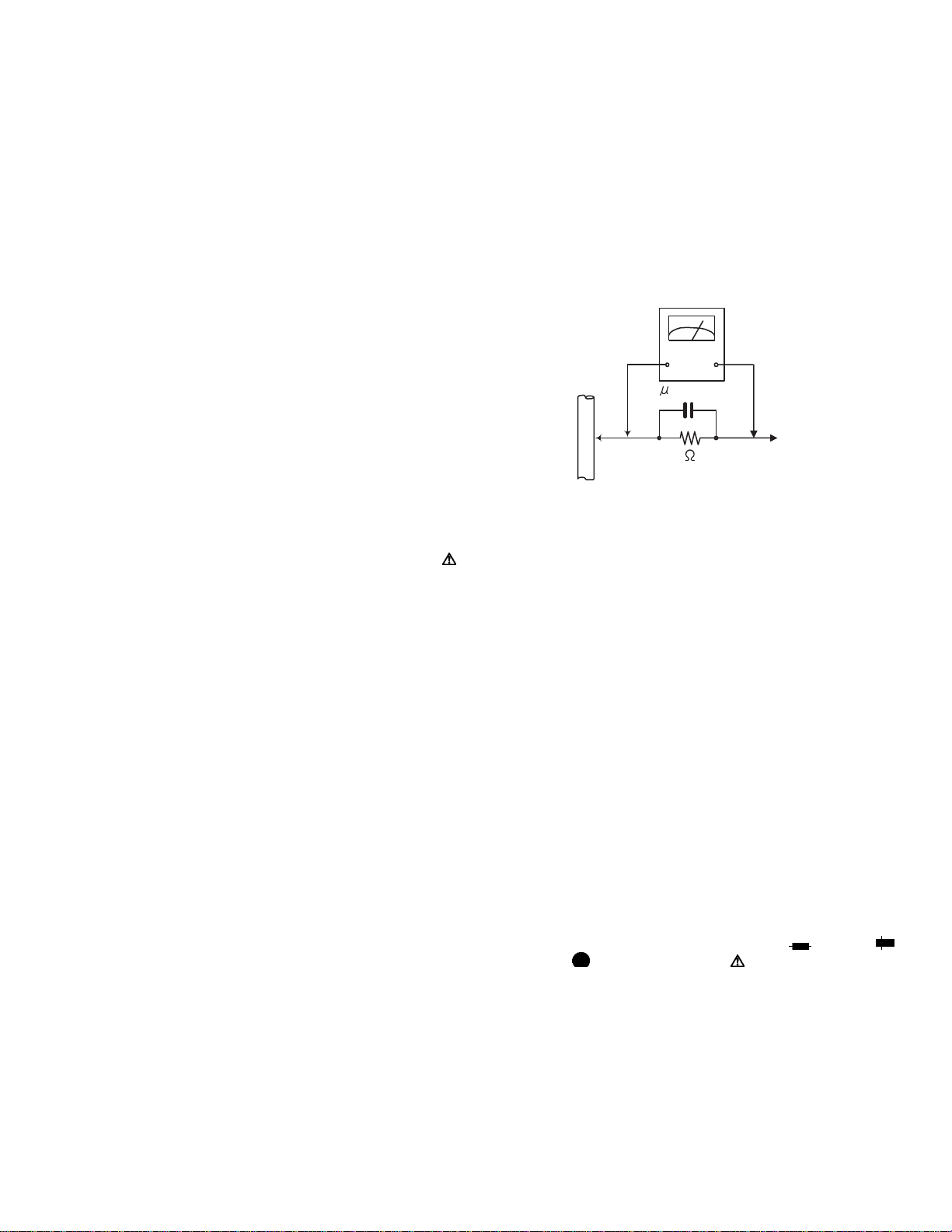
(5) Leakage shock hazard testing
After reassembling the product, always perform an isolation check on the exposed metal parts of the product (antenna terminals, knobs, metal cabinet, screw heads,
headphone jack, control shafts, etc.) to be sure the product
is safe to operate without danger of electrical shock.Do not
use a line isolation transformer during this check.
• Plug the AC line cord directly into the AC outlet. Using a
"Leakage Current Tester", measure the leakage current
from each exposed metal parts of the cabinet, particularly any exposed metal part having a return path to the
chassis, to a known good earth ground. Any leakage current must not exceed 0.5mA AC (r.m.s.).
• Alternate check method
Plug the AC line cord directly into the AC outlet. Use an
AC voltmeter having, 1,000
in the following manner. Connect a 1,500
paralleled by a 0.15
exposed metal part and a known good earth ground.
Measure the AC voltage across the resistor with the AC
Ω per volt or more sensitivity
Ω 10W resistor
µF AC-type capacitor between an
voltmeter.
Move the resistor connection to each exposed metal
part, particularly any exposed metal part having a return
path to the chassis, and measure the AC voltage across
the resistor. Now, reverse the plug in the AC outlet and
repeat each measurement. Voltage measured any must
not exceed 0.75 V AC (r.m.s.). This corresponds to 0.5
mA AC (r.m.s.).
(Having 1000
ohms/volts,
or more sensitivity)
0.15 F AC TYPE
Place this
probe on
1500 10W
1.2 Warning
(1) This equipment has been designed and manufactured to
meet international safety standards.
(2) It is the legal resp onsibility of the repairer to ensure that
these safety standards are maintained.
(3) Repairs must be made in accordance with the relevant
safety standards.
(4) It is essential that safety critical compone nts are replaced
by approved parts.
(5) If mains voltage selector is provided, check setting for local
voltage.
1.3 Caution
Burrs formed during molding may be left over on some parts
of the chassis.
Therefore, pay attention to such burrs in the case of preforming repair of this system.
1.4 Critical parts for safety
In regard with component parts appearing on the silk-screen
printed side (parts side) of the PWB diagrams, the parts that are
printed over with black such as the resistor ( ), diode ( )
and ICP ( ) or identified by the " " mark nearby are critical
for safety. When replacing them, be sure to use the parts of the
same type and rating as specified by the manufacturer.
(This regulation dose not Except the J and C version)
each expose
metal part.
(No.MB004)1-3
µ
Page 4
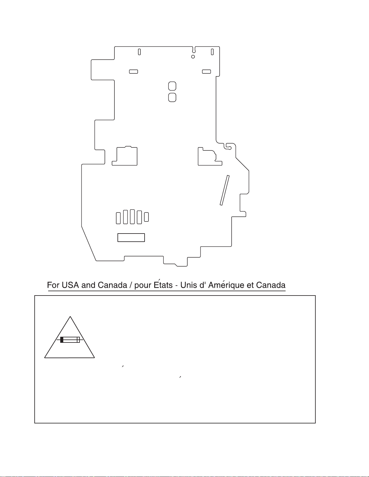
1.5 Importance administering point on the safety
Power supply board (Forward side)
F9101
Caution: For continued protection against risk of
fire, replace only with same type 5A/125V for
F9101.
This symbol specifies type of fast operating fuse.
Precaution: Pour eviter risques de feux, remplacez
le fusible de surete de F9101 comme le meme type
que 5A/125V.
Ce sont des fusibles suretes qui functionnes rapide.
^
1-4 (No.MB004)
Page 5

1.6 Preventing static electricity
Electrostatic discharge (ESD), which occurs when static electricity stored in the body, fabric, etc. is discharged, can destroy the laser
diode in the traverse unit (optical pickup). Take care to prevent this when performing repairs.
1.6.1 Grounding to prevent damage by static electricity
Static electricity in the work area can destroy the optical pickup (laser diode) in devices such as CD players.
Be careful to use proper grounding in the area where repairs are being performed.
(1) Ground the workbench
Ground the workbench by laying conductive material (such as a conducti ve sheet) or an iron plate over it before placing the
traverse unit (optical pickup) on it.
(2) Ground yourself
Use an anti-static wrist strap to release any static electricity built up in your body.
(caption)
Anti-static wrist strap
1M
Conductive material
(conductive sheet) or iron palate
(3) Handling the optical pickup
• In order to maintain quality during transport and before in stallation, both sides of th e laser diode on th e replacement optica l
pickup are shorted. After replacement, return the shorted parts to their original condition.
(Refer to the text.)
• Do not use a tester to check the condition of the laser diode in the optical pickup. The tester's internal power source can easily
destroy the laser diode.
1.7 Handling the traverse unit (optical pickup)
(1) Do not subject the traverse unit (optical pickup) to strong shocks, as it is a sensitive, complex unit.
(2) Cut off the shorted part of the flexible cable using nippers, etc. after replacing the optical pickup. For specific details, refer to the
replacement procedure in the text. Remove the anti-static pin when replacing the traverse unit. Be careful not to take too long
a time when attaching it to the connector.
(3) Handle the flexible cable carefully as it may break when subjected to strong force.
(4) I t is not possible to adjust the semi-fixed resistor that adjusts the laser power. Do not turn it.
1.8 Attention when traverse unit is decomposed
*Please refer to "Disassembly method" in the text for the CD pickup unit.
• Apply solder to the short land sections before the flexible wire is disconnected from the connecto r CN101
on the CD servo board.
(If the flexible wire is disconnected without applying solder, the CD pickup may be destroyed by static electricity.)
• In the assembly, be sure to remove solder from the short land sections after connecting the flexible wire.
Flexible wire
Short land section
CN601
CD servo board
(No.MB004)1-5
Page 6
1.9 Important for laser products
1.CLASS 1 LASER PRODUCT
2.DANGER : Invisible laser radiation when open and inter
lock failed or defeated. Avoid direct exposure to beam.
3.CAUTION : There are no serviceable parts inside the
Laser Unit. Do not disassemble the Laser Unit. Replace
the complete Laser Unit if it malfunctions.
4.CAUTION : The compact disc player uses invisible laser
radiation and is equipped with safety switches which
prevent emission of radiation when the drawer is open and
the safety interlocks have failed or are de
feated. It is dangerous to defeat the safety switches.
5.CAUTION : If safety switches malfunction, the laser is able
to function.
6.CAUTION : Use of controls, adjustments or performance of
procedures other than those specified herein may result in
hazardous radiation exposure.
!
Please use enough caution not to
see the beam directly or touch it
in case of an adjustment or operation
check.
1-6 (No.MB004)
Page 7

SECTION 2
SPECIFIC SERVICE INSTRUCTIONS
This service manual does not describe SPECIFIC SERVICE INSTRUCTIONS.
(No.MB004)1-7
Page 8

SECTION 3
A
A
DISASSEMBLY
3.1 Main body section
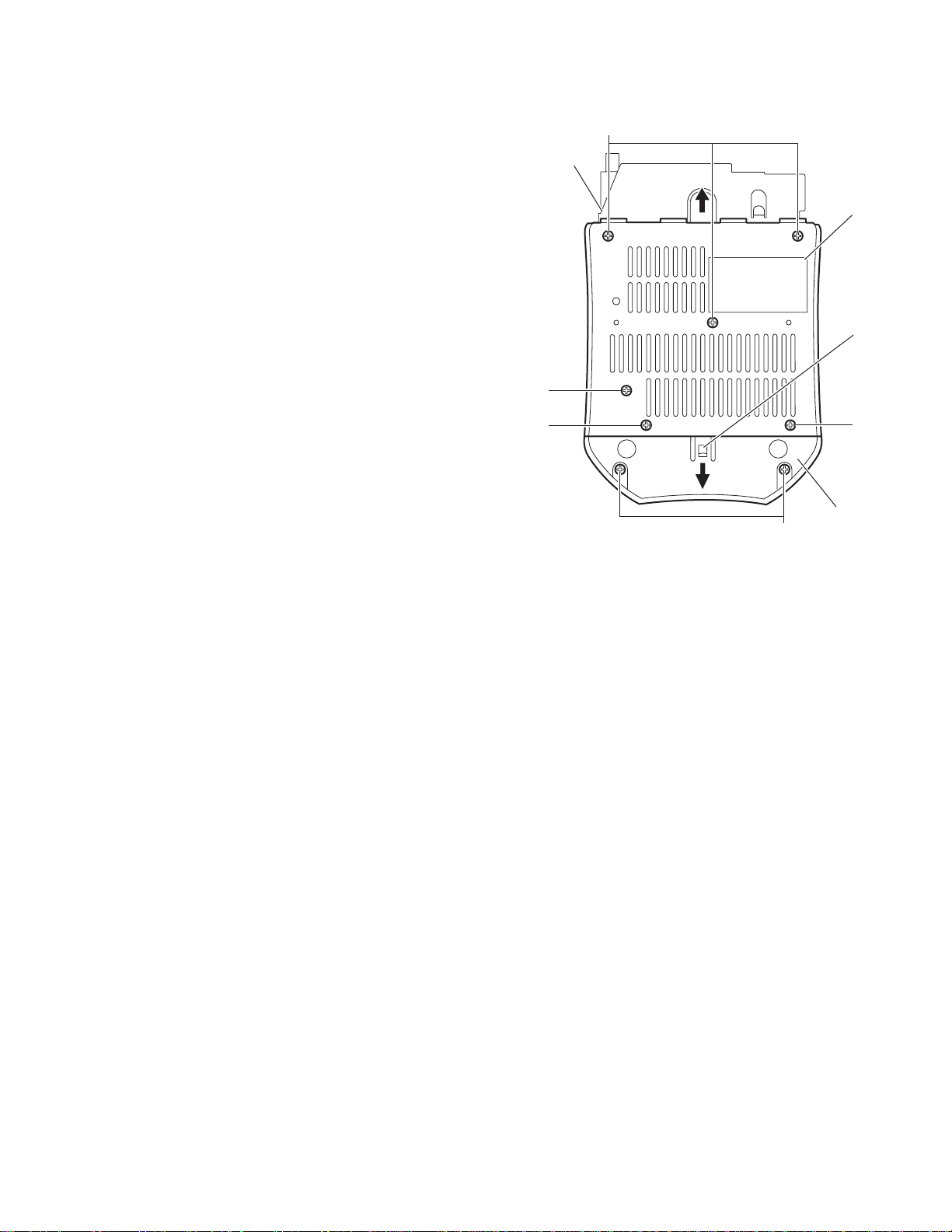
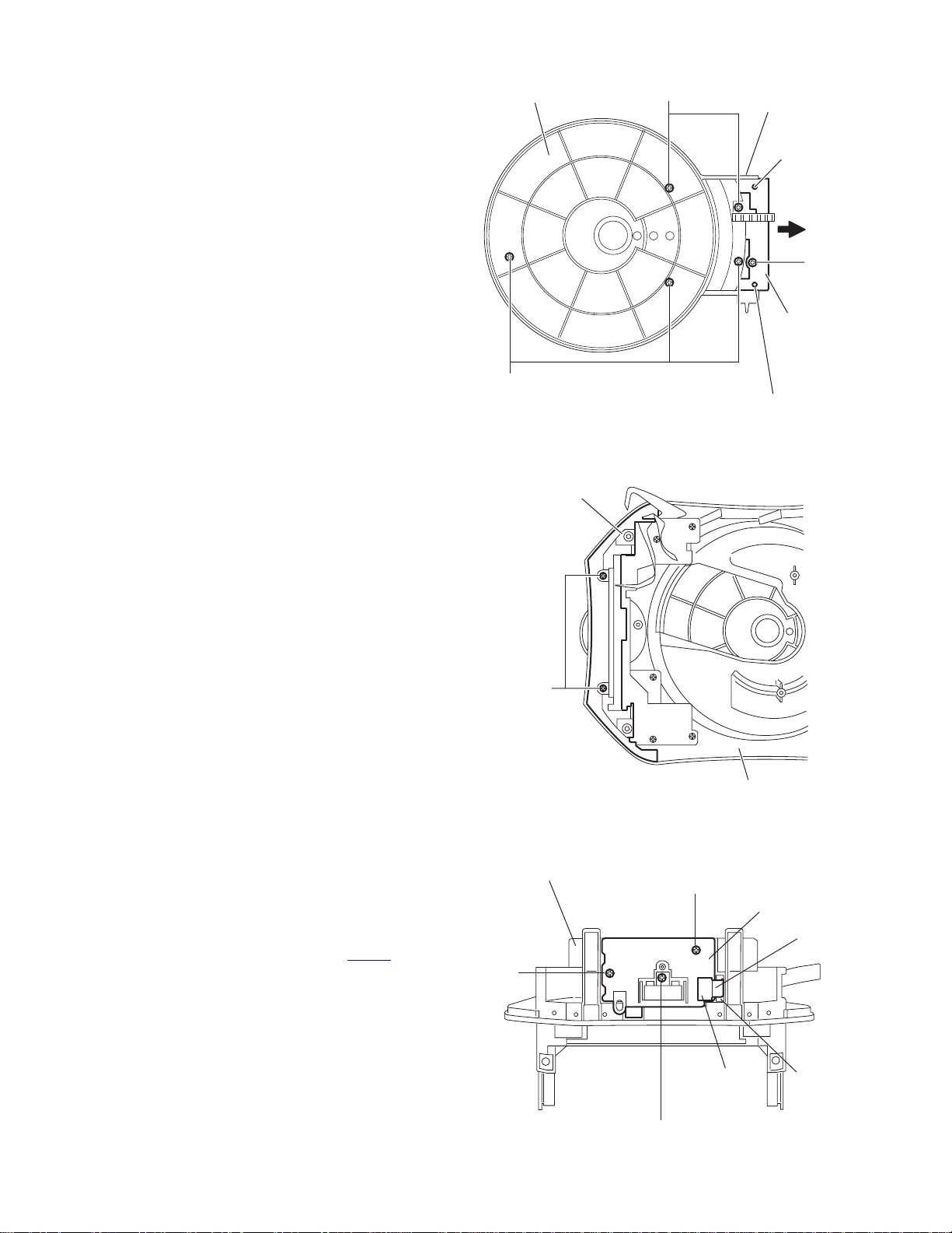
3.1.1 Removing the rear cover
(See Figs.1 and 2)
(1) From the back side of the mai n body, remove the fifteen
screws A attaching the rear cover. (See Fig.1.)
(2) Remove the two screws B attaching the fan cover. (See
Fig.1.)
(3) Remove the rear cover and disconnect the power cord
from the connector CN900
the main body. (See Fig.2.)
(4) Remove the strain relief in the di rection of the arrow. (See
Fig.2.)
Reference :
Before attaching the rear cover, pass the power cord through
the guide hole a on the rear cover. (See Fig.2.)
on the power supply board of
A A
B
Fan cover
Fuse
CN900
Fuse clip
B
Fig.1
Gurde hole a
Fig.2
A
Rear cover
Strain
relief
Power
supply
board
Power cord
Rear cover
1-8 (No.MB004)
Page 9
3.1.2 Removing the bottom case (A)
(See Fig.3)
• Prior to performing the following procedures, remove the rear
cover.
(1) From the bottom side of the main body, remove five screws
C and screw D attaching the bottom case (A).
(2) Remove the bottom case (A) in the direction of the arrow
while lifting the rear section of the bottom case (A).
3.1.3 Removing the bottom case (B)
(See Fig.3)
(1) From the bottom side of the main body, remove the two
screws E attaching the bottom case (B).
(2) Release the claw b of the bottom case (B) and remove the
bottom case in the direction of the arrow.
Note :
When turning the main body upside down to remove the bottom case (A) and the bottom case (B), place a cushion beneath the main body so as not to scratch the top case
assembly, volume control knob or other parts.
Bottom
chassis
D
C
C
Fig.3
E
Bottom
case (A)
Claw b
C
Bottom
case(B)
(No.MB004)1-9
Page 10
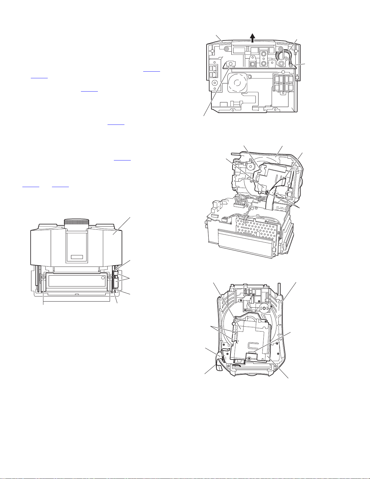
3.1.4 Removing the top case assembly
(See Figs.4 to 7)
• Prior to performing the following procedures, remove the rear
cover and bottom case (B).
(1) From the front side of the main body, remove the two
screws F attaching the top case assembly. (See Fig.4.)
(2) Disconnect the card wires from the connectors CN721
CN741 on the micon board. (See Fig.4.)
(3) From the back side of the main body, disco nnect the wire
from the connector CN451
Fig.5.)
(4) Remove the top case assembly while lifting it in the direc-
tion of the arrow. (See Fig.5.)
(5) From the inside of the to p case assembly, disconnect the
card wire from the connector CN651
board. (See Figs.6 and 7.)
Reference :
Reassembly of the top case assembly.
• Before reattaching the top case assemb ly to the main body,
connect the card wire to the connector CN651
board and hang it to the holder section c of the CD mechanism
assembly. (See Figs. 6 and 7)
• Let the card wire to be connected across the connectors
and CN741 go through the slit d on the top case as-
CN721
sembly. (See Fig. 7.)
on the function board. (See
on the CD servo
on the CD servo
and
Top case asembly
Function board
CD mechanism assembly
CD servo board
Wire
CN451
Fig.5
Top case assembly
CN651
F
Fig.4
Top case assembly
CN741
Card wires
CN721
Micon board
CD servo board
Holder
section c
Notch d
Card wire
Fig.6
Top case assembly
CN651
CD mechanism assembly
Fig.7
Holder
section
c
1-10 (No.MB004)
Page 11

3.1.5 Removing the tuner
r
(See Fig.8)
• Prior to performing the following procedures, remove the rear
cover, bottom case (B) and top case assembly.
(1) From the right side of the main body, disconne ct the card
wire from the connector CN1
on the tuner.
CN1
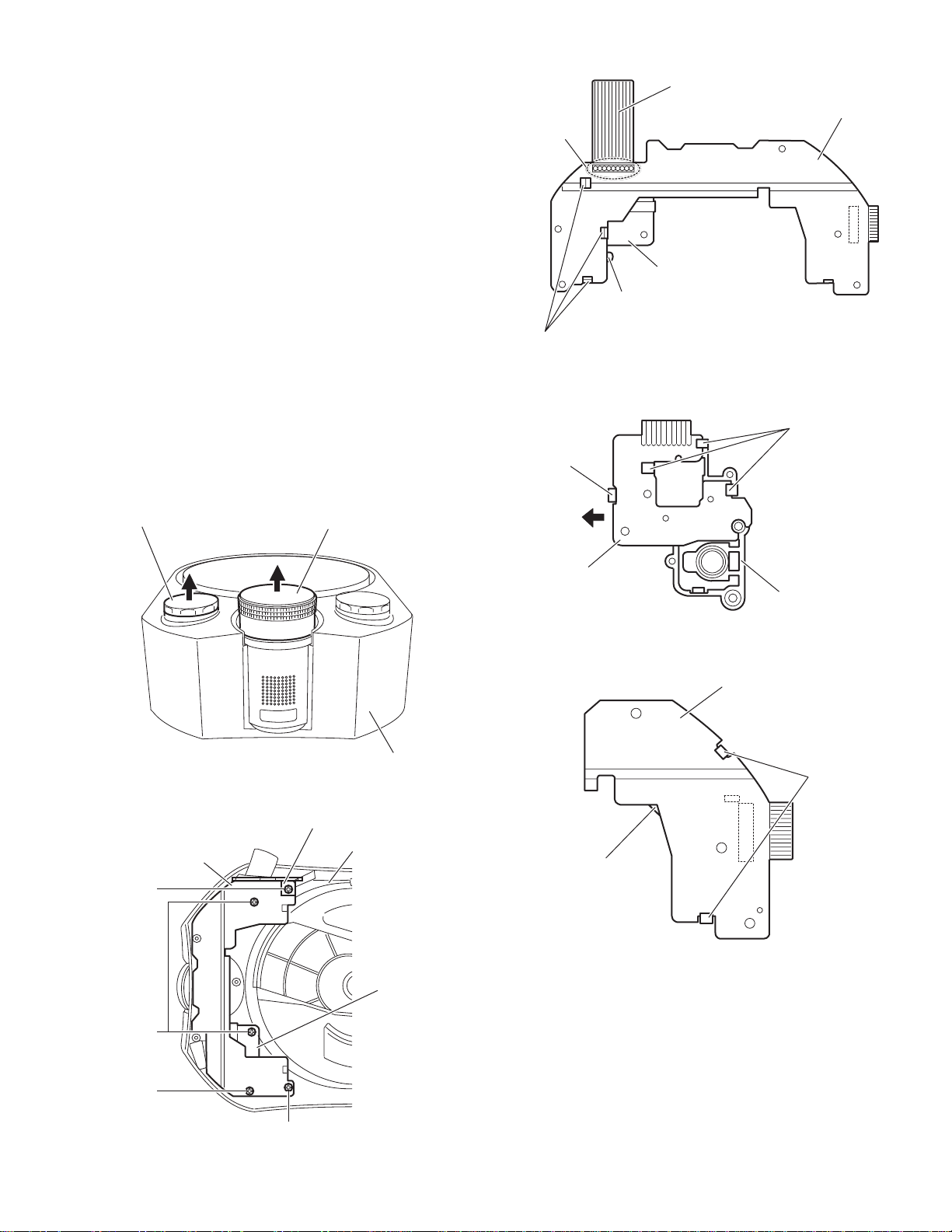
3.1.6 Removing the function board
(See Fig.9)
• Prior to performing the following procedures, remove the rear
cover, bottom case (B) and top case assembly.
(1) From the top side of the main body, disconnect the fan mo-
tor wire from the connector CN942
(2) Disconnect the wires from the connectors CN893
CN895 on the function board.
(3) Remove the spacer and tie band fixing the wires.
(4) Disconnect the wire from the connector CN301
ital amplifier board.
(5) Remove the three screws G attaching the function board.
(6) Lift the function board in the direction of the arrow and dis-
connect it from the connector CN951
board.
Reference :
When connecting the fan motor wire, put it through the slit e of
the function board.
on the function board.
and
on the dig-
on the digital amplifier
Tie band
CN301
Wire
Card wire
Digital amplifier
board
Spacer
Fig.8
CN942
G
CN893
Fig.9
Tune
CN951
G
Wire
CN895
G
Slit e
Fan motor
Function board
Fan motor wire
3.1.7 Removing the micon board
(See Fig.10)
• Prior to performing the following procedures, remove the rear
cover, bottom case (A), bottom case (B) and top case assembly.
(1) From the right side of the main body, remove the tie bands
bundling the wires.
(2) Disconnect the wire from the connector CN805
con board.
(3) Disconnect the card wires from the connectors CN661
CN871 on the micon board.
(4) Disconnect the wire from the connector CN893
tion board.
(5) Remove the two screws H and two screws J attaching the
micon board.
(6) Pull the micon board toward this side, disconnect the con-
nectors CN801
Reference :
• After connecting the card wire to the connector CN661
the micon board, bend it as was done before disassembly
and insert it inside the center chassis.
• After connecting the wires to the connectors (CN805
CN893
) on the micon and function boards, bundle the wires
with the tie bands.
and CN802 on the micon board.
on the mi-
and
on the func-
on
Micon board
CN805
Wire
Tie bands
Fanction board
CN893
H
H
J
CN801
CN661
,
CN802
Card wire
Fig.10
J
CN871
Card wire
(No.MB004)1-11
Page 12

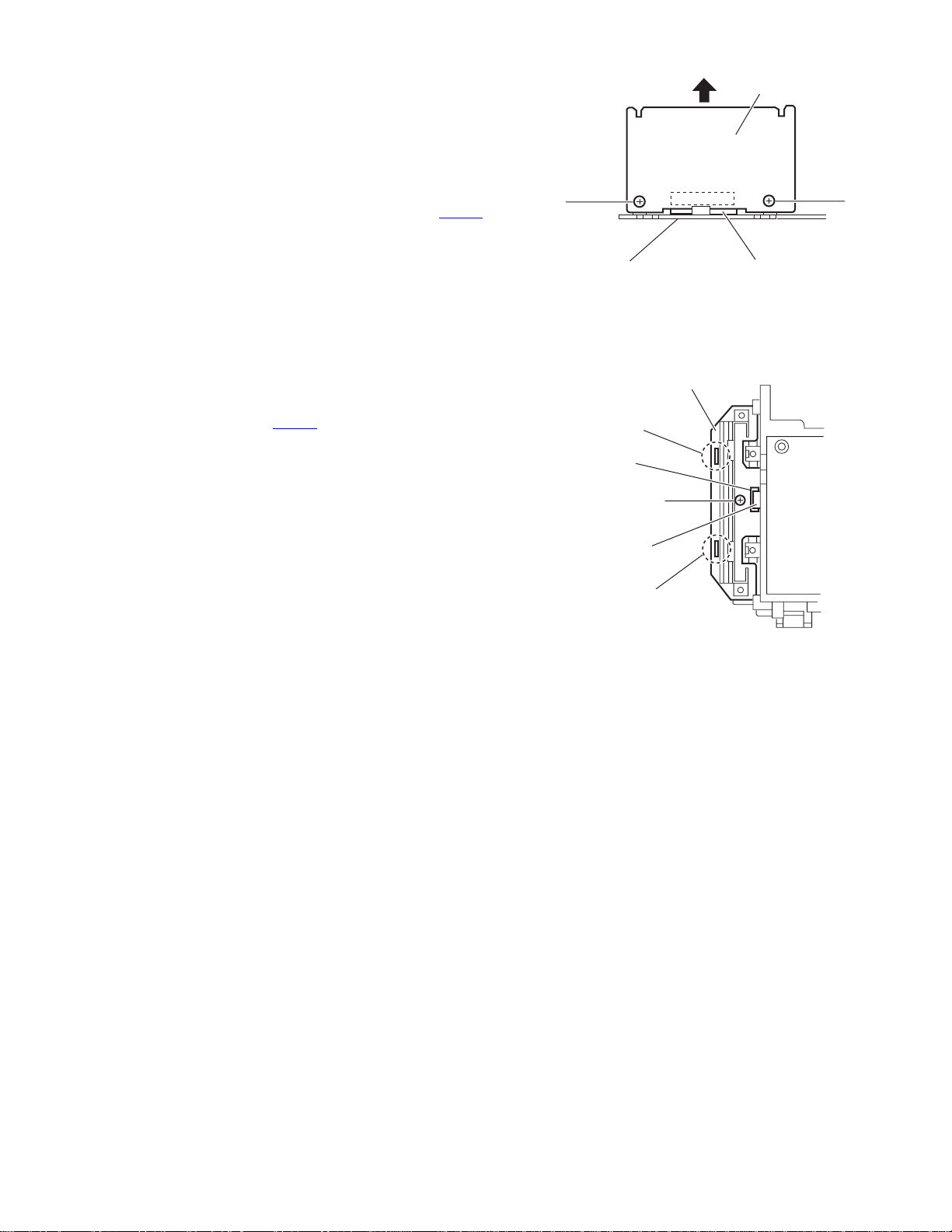
3.1.8 Removing the digital amplifier board
(See Fig.11)
• Prior to performing the following procedures, remove the rear
cover, bottom case (A), bottom case (B) and top case assembly.
(1) From the left side of the main body, disconnect the wire
from the connector CN301
(2) Remove the spacer and tie band fixing the wire.
(3) Remove the two screws K, two screws L and screw L' at-
taching the digital amplifier board.
(4) Pull the digital amplifier board toward this side, disconnect
the connectors CN961
board.
Reference :
• When attaching the screw L', attach the ea rth w ire togeth er
it.
• After connecting the wire, fix the wire with the spacer and tie
band.
3.1.9 Removing the power supply board
(See Figs.12 to 14)
• Prior to performing the following procedures, remove the rear
cover, bottom case (A), bottom case (B), top case assembly,
tuner, function board, micon board and digital amplifier board.
(1) From the top side of the main body, remove the two screws
M attaching the center chassis. (See Fig.12.)
(2) From the bottom side of the main bo dy, remove the two
screws N attaching the power supply board. (See Fig.13.)
(3) Disconnect the card wire from the connector CN903
power supply board. (See Fig.14.)
(4) Remove the three screws P attaching the power supply
board. (See Fig.14.)
(5) Remove the barrier (E) and barri er (F) under the power
supply board. (See Fig.14.)
Reference :
• Before attaching the each parts, pass the card wire through
the holes f on the center chassis.
• After attaching the center chassis, put the earth wire through
the slit g of the power supply board and sections h of the
center chassis.
Card wire
on the digital amplifier board.
and CN981 on the digital amplifier
on the
Hole f
Center chassis
Digital amplifier board
CN981
CN961
Earth Wire
L
N
N
K
Spacer
CN301
L'
Fig.11
Power supply board
Bottom chassis
Fig.13
Power supply board
P
Tie band
K
Wire
L
Card wire
Bottom chassis
Earth wire
1-12 (No.MB004)
Slit g
Fig.12
Section h
M
M
P
Barrier (E)
Barrier (F)
P
CN903
Fig.14
Page 13
3.1.10 Removing the regulator board
(See Fig.15)
• Prior to performing the following procedures, remove the rear
cover, bottom case (A), bottom case (B), top case assembly,
tuner, function board, micon board, digital amplifier board and
power supply board.
(1) From the side of the power supply board, remove the two
screws Q attaching the regulator board.
(2) Disconnect the regulator board from the connector CN931
on the power supply board in the direction of the arrow.
Q
Regulator board
Q
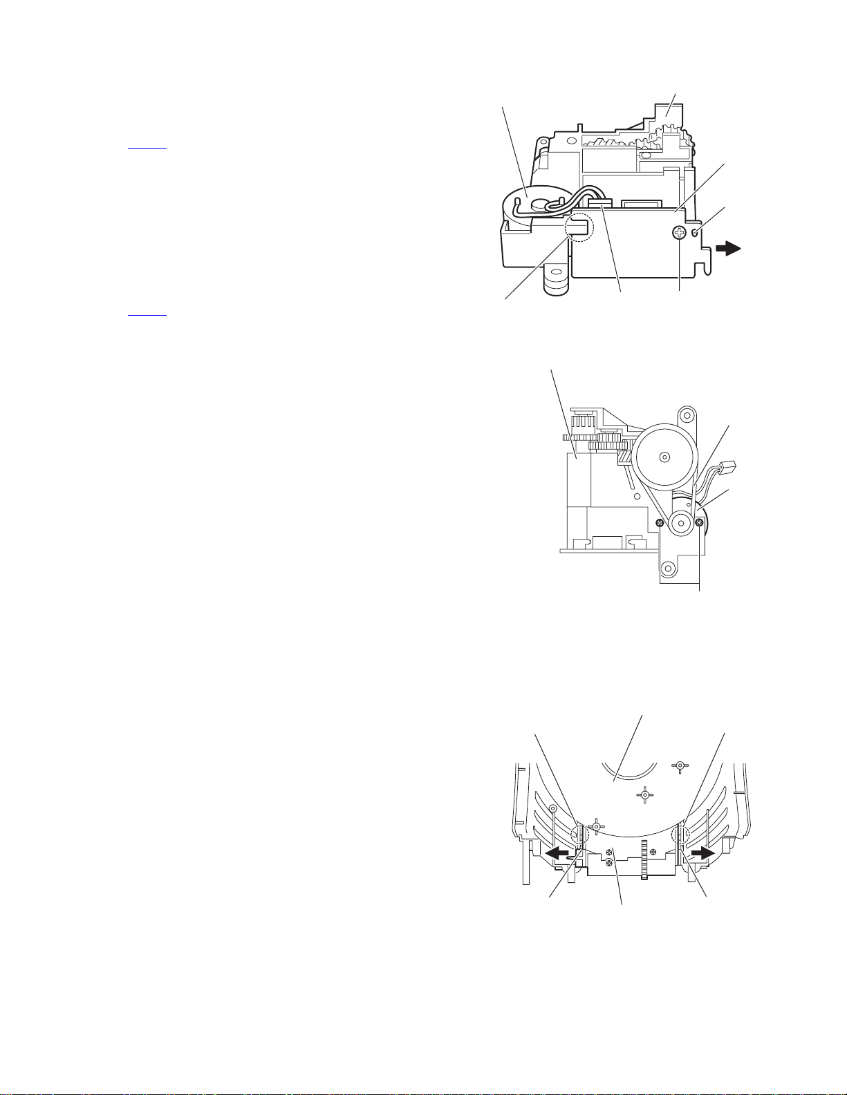
3.1.11 Removing the FL board
(See Fig.16)
• Prior to performing the following procedures, remove the rear
cover, bottom case (B) and top case assembly.
(1) From the top side of the main bo dy, disconnect the card
wire from the connector CN751
(2) Remove the screw R attaching the FL board.
(3) Release the two engagement sections i of the bottom
chassis, take out the FL board.
on the FL board.
Power supply board
FL board
Engagement
section i
CN751
R
Card wire
Engagement
section i
CN931
Fig.15
Fig.16
(No.MB004)1-13
Page 14

3.2 Top case assembly section
• Prior to performing the following procedures, remove the top
case assembly.
Note :
Be careful not to scratch the top case, volume control knob or
other parts.
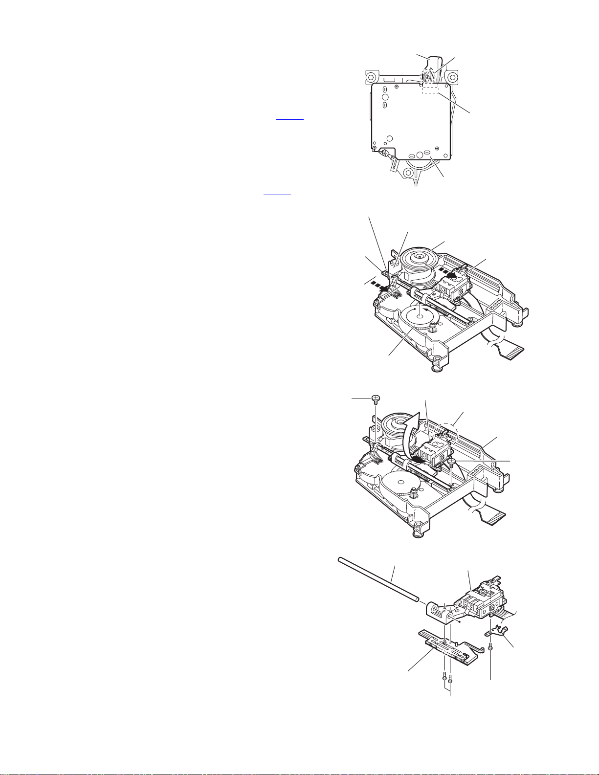
3.2.1 Removing the CD mechanism assembly
(See Fig.17)
(1) From the inside of the top case assembly, remove the three
screws S attaching the CD mechanism assembly.
(2) Take out the CD mechan ism assembly from the top case
assembly.
3.2.2 Removing the CD door mechanism assembly
(See Figs.17 and 18)
(1) Remove the cover in the direction of the arrow. (See
Fig.17.)
(2) From the inside of the to p case assembly, disconnect the
wire from the connector CN461
board. (See Fig.17.)
(3) Remove the three screws T attaching the gear bracket and
take out the gear bracket. (See Fig.17.)
(4) Remove the two screws U attaching the CD door mecha-
nism assembly and take out the CD door mechanism assembly. (See Fig.17.)
Reference :
Before attaching the CD door mechanism assembly, put the
wire through the two slits j of the CD door mechanism assembly and then attach the two screws U. (See Figs.17 and 18.)
on the CD door switch
Top case assembly
CD mechanism assembly
S
T
Gear bracket
U
Fig.17
CD door
mechanism assembly
CD door
mechanism
assembly
T
Cover
CD door
switch
board
CN461
Fig.18
Slits j
1-14 (No.MB004)
Page 15
3.2.3 Removing the CD door switch board
r
(See Fig.19)
• Prior to performing the following procedure s, remove the CD
door mechanism assembly.
(1) Disconnect the wire of the CD door motor from the connec-
tor CN452
(2) Remove the screw V attaching the CD door switch board.
(3) Release the CD door switch bo ard from the projection k
and then remove it from the engagement section m in the
direction of the arrow.
3.2.4 Removing the CD door motor
(See Figs.19 and 20)
• Prior to performing the following procedure s, remove the CD
door mechanism assembly.
(1) Disconnect the wire of the CD door motor from the connec-
tor CN452
(2) Turn over the CD door mech anism assembly and remove
the belt. (See Fig.20.)
(3) Remove the two screws W attaching the CD doo r motor.
(See Fig.20.)
Note :
Take care not to attach grease of the gears on the belt.
on the CD door switch board.
on the CD door switch board. (See Fig.19.)
CD door motor
Engagement section m
CD door mechanism assembly
CN452
Fig.19
CD door
mechanism assembly
CD door
switch board
Projection k
V
Belt
3.2.5 Removing the CD door assembly
(See Fig.21)
• Prior to performing the following procedure s, remove the CD
mechanism assembly and CD door mechanism assembly.
(1) From the inside of the top case assembly, remove the boss
p of the CD door assembly while extending the section n of
the top case assembly in the direction of the arrow.
(2) Remove the boss r of the CD door assembly while extend-
ing the section q of the top case assembly in the direction
of the arrow.
Section q
CD doo
motor
W
Fig.20
Top case assembly
Section n
Boss r
CD door assembly
Fig.21
Boss p
(No.MB004)1-15
Page 16
3.2.6 Removing the CD door LED board
(See Fig.22)
• Prior to performing the following procedures, remove the CD
mechanism assembly, CD door mechanism assembly and CD
door assembly.
(1) From the reverse side of the CD door assembly, remove
the five screws X attaching the CD door cover.
(2) Remove the screw X attaching the CD door LED board.
(3) After removing the CD door cover, remove the CD door
LED board from the projections (s, t) and take out it in the
direction of the arrow.
CD door cover
X
CD door
Projection s
X
CD door
LED board
3.2.7 Removing the front holder assembly
(See Fig.23)
• Prior to performing the following procedures, remove the CD
mechanism assembly.
(1) From the inside of the top case assembly, remove the two
screws Y attaching the front holder assembly.
(2) Take out the front holder assembly.
3.2.8 Removing the front board
(See Fig.24)
• Prior to performing the following procedures, remove the CD
mechanism assembly and front holder assembly.
(1) From the forward side of the front holder assembly, remove
the three screws Z attaching the front board.
Reference :
• Remove the card wire from the connector CN731
front board as required.
• Before attaching the front board, pass the card wire through
the hole u on the front holder assembly.
on the
X
Projection t
Fig.22
Front holder assembly
Y
Top case assembly
Fig.23
Front holder assembly
Z
Front board
Card wire
Z
1-16 (No.MB004)
Z
Fig.24
CN731
Hole u
Page 17
3.2.9 Removing the volume board and LED board
A
(See Figs.25 to 29)
• Prior to performing the following procedure s, remove the CD
mechanism assembly and front holder assembly.
(1) From the top side of the top case assembly, pull out the vol-
ume and function knobs. (See Fig.25.)
(2) From the inside of the top case assembly, remove the three
screws AA and screw AA' attaching the volume board.
(See Fig.26.)
Reference :
When attaching the screw AA', attach the barrier (D) together it.
(3) Remove the screw AA attaching the LED board. (See
Fig.26.)
(4) Take out the volume board together the LED board.
(5) From the reverse side of the volume board , release the
three claws v attaching the push button (A). (See Fig.27.)
(6) Remove the solders from the soldered section w on the vol-
ume board and disconnect the parallel wire. (See Fig.27.)
(7) Release the claw x of the push button (A) and remove the
LED board from the engagement section y of the push but-
ton (A) in the direction of the arrow. (See Fig.28.)
(8) Release the claw z of the button base (B) and remove the
button base (B) from the volume board. (See Fig.29.)
Soldered
section w
Claw v
Claw x
Parallel wire
Volume board
LED board
Push button (A)
Fig.27
Engagement
sections y
Function knob
Volume board
A'
Volume knob
Fig.25
Barrier (D)
Top case assembly
Top case assembly
LED board
LED board
Button base(B)
Fig.28
Volume board
Fig.29
Push button (A)
Claws
z
AA
AA
AA
Fig.26
(No.MB004)1-17
Page 18

3.3 CD mechanism assembly section
• Prior to performing the following procedures, remove the CD
mechanism assembly.
3.3.1 Removing the CD traverse mechanism assembly
(See Figs.1 and 2)
(1) From the forward side of the CD traverse mechanism as-
sembly, release the two join ts a attaching the pickup cover
to the CD traverse mechanism assembly. (See Fig.1.)
(2) Remove the three screws A attaching the CD traverse
mechanism assembly to the CD mechanism holder and
take out the CD traverse mechanism assembly. (See
Fig.1.)
Reference :
After attaching the assist spring to the CD mechanism holder,
attach the CD traverse mechanism assembly to the CD mechanism holder. (See Fig.2.)
A
CD traverse
mechanism
assembly
Joints a
3.3.2 Removing the CD servo board
(See Fig.3)
• Prior to performing the following procedures, remove the CD
traverse mechanism assembly.
Caution :
Be sure to solder the short land section b on the flexib le wire
before disconnecting the flexible wire fro m connector CN601
on the CD servo board.
If the flexible wire is disconnected without attaching solder, the
pickup may be destroyed by static electricity.
(1) From the reverse side of the CD traverse mechanism as-
sembly, solder the short land section b on the flexible wire.
(2) Disconnect the flexible wire from the connector CN601
the CD servo board.
(3) Remove the three screws B attaching the CD servo board.
(4) Remove the solders from the two soldered section c and d,
remove the CD servo board in an upward direction.
Caution :
When attaching the CD servo board, be sure to remove the
solder from the short land section b after connecting the flexible wire.
on
CD pickup cover
A
Fig.1
CD traverse mechanism assembly
CD mechanism holder
Fig.2
Flexible wire
B
soldered
section c
B B
soldered section d
CD traverse mechanism assembly
Fig.3
CD mechanism holder
Assist spring
Short land section b
CN601
CD servo board
1-18 (No.MB004)
Page 19
3.3.3 Removing the pickup assembly
(See Figs.4 to 7)
• Prior to performing the following procedure s, remove the CD
traverse mechanism assembly.
Caution :
Be sure to solder the short land section b on the flexible wire
before disconnecting the flexible wire from connector CN601
on the CD servo board.
If the flexible wire is disconnected without attaching solder, the
pickup may be destroyed by static electricity.
(1) From the reverse side of the CD traverse mechanism as-
sembly, solder the short land section b on the flexible wire.
(See fig.4.)
(2) Disconnect the flexible wire from the connector CN601
the CD servo board. (See fig.4.)
(3) From the top side of the CD traverse mechanism assem-
bly, turn the middle gear in the direction of the arrow so that
the pickup assembly is shifted to the reverse side of the
turn table assembly.
Move the pickup assembly until the section e of the rack
plate in the lower section of the pickup assembly comes out
of the chassis base assembly. (See fig.5.)
(4) Remove the two screws C attaching the shaft of the pickup
assembly. Next, disengage the hook f from the chassis
base assembly and then remove the pickup assembly with
the shaft. (See fig.6.)
(5) Pull the shaft out of the pickup assembly. (See fig.7.)
(6) Remove the two screws D attaching the rack plate to the
pickup. (See fig.7.)
(7) Remove the screw E attaching the P.S.spring to the pick-
up. (See fig.7.)
on
Rack plate
Section e
Middle gear
C
Flexible wire
CD servo board
Chassis base assembly
Pickup assembly
Short land section b
CN601
Fig.4
Turn table assembly
Pickup assembly
Fig.5
Section f
Shaft
Rack plate
Chassis assembly
C
Fig.6
Pickup
P.S.spring
E
D
Fig.7
(No.MB004)1-19
Page 20
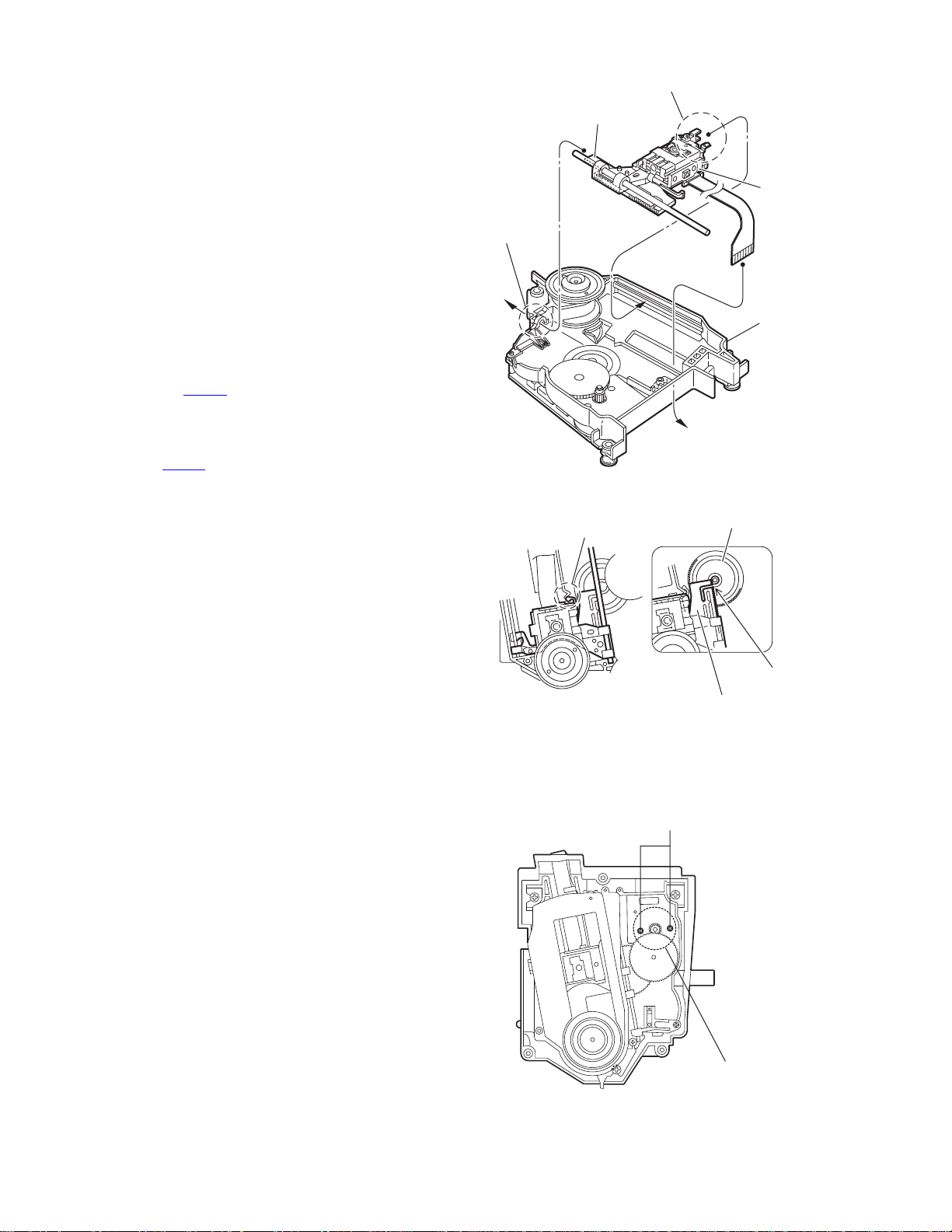
3.3.4 Reinstalling the pickup assembly
(See Figs.8 and 9)
Reference :
Refer to the explanation of "Removing the pickup assembl y"
on the preceding page.
(1) Attach the P.S.spring and rack plate to the pickup.
(2) Insert the shaft into the pickup.
(3) Engage the hook f of the pickup assembly to the chassis
base assembly first, and set the section e of the rack plate
in the opening section g.
Then reinstall the pickup assembly while shifting it to the
turn table assembly side (inward) so that the section h of
the rack plate is positioned as shown in Fig.9.
(4) Move the pickup assembly to the center position and fasten
the shaft with the two screws C. (Make sure that the section
i of the rack plate is correctly engaged with the rack gear.)
(5) After passing the flexible wire of the pickup through the
opening section of the chassis base assembly, connect it
to the connector CN601
Note :
When reinstalling the pickup assembly, remove the solder
from the short land section b after connecting the flexible wire
to the connector CN601
on the CD servo assembly.
on the CD servo board.
Section f
Section e
Pickup
assembly
Section g
Chassis base
assembly
Fig.8
3.3.5 Removing the feed motor assembly
(See Fig.10)
• Prior to performing the following procedures, remove the CD
traverse mechanism assembly and CD servo board.
From the forward side of the CD traverse mechanism assembly, remove the two screws F attaching the feed motor assembly.
Section h
Rack gear
Section i
Rack plate
Fig.9
F
1-20 (No.MB004)
Feed motor assembly
Fig.10
Page 21
4.1 Test instruments require d for ad justment
(1) Digital oscilloscope
(2) Electric voltmeter
(3) Test disk : CTS-1000
4.2 Adjusting and confirming contents
4.2.1 Adjustment of the CD section
(1) Indication of the C1 error (CD test mode 1)
(2) Indication of the auto adjusting value (CD test mode 2)
(3) Cancellation of the test mode
4.2.2 System test mode (FL all lighting-up check)
4.3 Adjusting and confirming methods
4.3.1 Adjusting and confirming of the CD sectio n
(1) Indication of the C1 error (CD test mode 1)
While pressing both the STOP and
AHB plus buttons on the main
unit, turn on the primary power supply.
SECTION 4
ADJUSTMENT
Press the STANDBY/ON button
on the main unit.
FL indication
CD TEST MODE 1
Press the OPEN/CLOSE button
on the main unit and insert the
test disc.
Press key 1, 2 or 4 of the remote control
unit to start measurement. The number of
error corrections will be displayed every 10
seconds.
Key 1: Normal-speed playback
Key 2: 2x-speed playback
Key 4: 4x-speed playback
FL indication
x1 Err
x2 Err
x4 Err
(No.MB004)1-21
Page 22

(2) Indication of the auto adjusting value (CD test mode 2)
While pressing both the STOP and
AHB plus buttons on the main
unit, turn on the primary power supply.
Press the STANDBY/ON button
on the main unit.
FL indication
CD TEST MODE 1
Wait a moment while keeping to
press the SET key on the remote
controller.
FL indication
CD TEST MODE 2
Press the SET key on
the remote controller.
FL indication
:
Description of the indication
:
Adjusting value
Each time the SET key
on the remote controller
is pressed, the indication
changes from FG to AOC1.
FG
Mantissa part of the focus gain
FEXP
Characteristic part of the focus gain
E2 status
E3 status
E1 status
FBAL
Adjusting value of the focus balance
FOFS
Adjusting value of the focus offset
FES
Disturbance amplitude during the focus gain adjustment
TG
Mantissa part of the tracking gain
TEXP
Characteristic part of the tracking gain
TBAL
Tracking balance adjusting value
TOFS
Tracking offset adjusting value
TES
Disturbance amplitude during the tracking gain adjustment
FAGC
Focus precise gain
ABC2
Tracking balance
ABC1
Focus balance
AGC2
Tracking coarse gain
AGC1
Focus coarse gain
AOC1
Focus offset
Press the CANCEL key
on the remote controller.
FL indication
CD TEST MODE 1
(3) Cancellation of the test mode
To cancel the test mode, press the STANDBY/ON button on the main unit.
1-22 (No.MB004)
Page 23

4.3.2 System test mode (FL all lighting-up check)
Go to the Adjustment Mode.
Press the "2", "STOP" and "STANDBY/ON"
keys on the remote controller simultaneously.
FL indication
All lighting-up
By pressing any of the keys on the
remote controller, the initial display
screen is resumed.
By pulling out the power supply cord of the
main unit the test mode will be canceled.
In the adjustment mode a 1-second real-time
increment sets the clock to gain 1 minute.
(No.MB004)1-23
Page 24

TROUBLE SHOOTING
5.1 Flow of functional operation until TOC read
Power ON
Disc play Key
Automatic tuning of FO offset and TE offset
SECTION 5
Slider turns REST
SW ON.
Laser ON
Detection of disc
Check Point
Confirm that the voltage at
the pin32 of IC251 is 0V.
(ON: 0V)
Tracking error waveform at TOC reading
IC601
20pin(TEOUT)
Approx.
1.4V
VREF
Disc status
to rotate
Approx. 3sec
Tracking
servo
off status
Automatic measurement
of TE amplitude and
automatic tuning of TE
balance
Tracking
servo
on status
Disc to be
braked to stop
TOC reading
finishes
500mv/div
2ms/div
Fig.1
Automatic measurement of
Focus S-curve amplitude
Disc is rotated
Focus servo ON
(Tracking servo ON)
Automatic measurement of
Tracking error amplitude
Automatic tuning of
Tracking error balance
Automatic tuning of
Focus error balance
Automatic tuning of
Focus error gain
Confirm that the Focus error
S-curve signal at the pin32 of
IC651 is approx. 1.4Vp-p.
Confirm that the signal from
pin24 of IC651(one side of
R808) is 0V as a accelerated
pulse during approx. 640ms.
Confirm the waveform of the
Tracking error signal at the
pin20 of IC601(one side of
R604) (See Fig.1.)
1-24 (No.MB004)
Automatic tuning of
Tracking error gain
TOC reading
Play a disc
Confirm the eye-pattern
at the pin5 of IC601
Page 25

5.2 Maintenance of laser pickup
(1) Cleaning the pickup lens
Before you replace the pickup, please try to clean the lens
with a alcohol soaked cotton swab.
(2) Life of the laser diode
When the life of the laser diode has expired, the following
symptoms will appear.
Is RF output
0.9 0.22Vp-p?
NO
Replace it.
5.3 Replacement of laser pickup
Turn of the power switch and, disconnect the
power cord.
Replace the pickup with a normal one. (Refer
to "Pickup Removal" on the previous page)
YES
O.K
(3) The level of RF output (EFM ou tput, amplitude of eye pat-
tern: pin5 of IC601) will be low.
(4) Semi-fixed resistor on the APC PC board
The semi-fixed resistor on the APC printed circuit board
which is attached to the pickup is used to adjust the laser
power. Since this adjustment should be performed to
match the characteristics of the whole optical block, do not
touch the semi-fixed resistor. If the laser power is lower
than the specified value, the laser diode is almost worn out,
and the laser pickup should be replaced. If the semi-fixed
resistor is adjusted while the pickup is functioning normally,
the laser pickup may be damaged due to excessive current.
Plug the power cord in, and turn the power on.
At this time, check that the laser emits for
about 3 seconds and the objective lens moves
up and down.
Note: Do not observe the laser beam directly.
Play a disc.
Check the eye-pattern at 5pin of IC601.
Finish.
(No.MB004)1-25
Page 26

VICTOR COMPANY OF JAPAN, LIMITED
AV & MULTIMEDIA COMPANY AUDIO/VIDEO SYSTEMS CATEGORY 10-1,1chome,Ohwatari-machi,Maebashi-city,371-8543,Japan
(No.MB004)
Printed in Japan
WPC
Page 27

SCHEMATIC DIAGRAMS
COMPACT COMPONENT SYSTEM
FS-X3,FS-X1
CD-ROM No.SML200308
Area suffix
J ----------------------------- U.S.A.
C -------------------------- Canada
SP-FSX3 SP-FSX3CA-FSX3
SP-FSX1 SP-FSX1CA-FSX1
Contents
Block diagram
Standard schematic diagrams
Printed circuit boards
COPYRIGHT 2003 VICTOR COMPANY OF JAPAN, LTD.
2-1
2-3
2-13 to 21
No.MB004SCH
2003/8
Page 28

In regard with component parts appearing on the silk-screen printed side (parts side) of the PWB diagrams, the
parts that are printed over with black such as the resistor ( ), diode ( ) and ICP ( ) or identified by the " "
mark nearby are critical for safety.
(This regulation does not correspond to J and C version.)
Page 29

< MEMO >
2-11
Page 30

Block diagram
F
F
/
R
Q
U
TUNER
MODULE
Front board
IC731
REMOCON
RECEIVER
STANDBY/ON
SWITCH
STANDBY
/POWER ON
LED
Volume board
VOL/FUNCTION
SWITCH
OPERATION
SWITCH
, , ,
CD OP/CL
AHB PRO
FW701
CN731
CN711
Micon board
L/R
CN871
TUDAIN
TUCLK
TUDAOUT
TUCE
CN741
KEY3
V.JOGA
V.JOGB
F.JOGA
F.JOGB
CN721
CDIND
FMIND
AMIND
LINEIND
KEY1 to KEY3
S-IND
P-IND
RMIN
VJOGA
VJOGB
FJOGA
FJOGB
CDIND
FMIND
AMIND
LINEIND
KEY1
KEY2
L8101,L8201
DOLBY
FILTER
IC801
SYSTEM
MICON
TUL
TUR
SMUTE
LMUTE
MT0
MT1
MTS
VOLCE
VOLCLK
VOLDATA
AHB1
CLSW
OPSW
BUZZER
TOPIND
OLOAD
MODON
F-SHIFT
PRT
THERM
CDDOUT
CDCMND
CDSTAT
CDREQ
CDCLK
CDRST
BUZZER
ALARM2
ALARM3
POWERFL
FLDATA
FLCLK
FLSTB
FLBK
POWER
INH
BSTCTL
BEAT1
BEAT2
FTU
MI+6.0V,A+10V
CD+7.5V
CDL
CDR
THERM
LINE OUT L/R
DIGITAL OUT
CN805
MOTOR
CN661
W803
CN802
CN801
J4311
LINE IN L/R
J4341
FAN
M
Function board
LINE OUT L
LINE OUT R
CDDOUT
CN895
CN942
Q9431
Q9432
FAN SW.
CN893
CD+7.5V
A+10V
MI+5V
CD servo board
OUTL
CN651
OUTR
TX
KCMND
M STAT
MRDY
KCLK
MCS
UNIT MICON
CN902
CN901
CN931
Q4111,Q4211
Q4311
L.O.MUTE
LMUTE
THERM
IC651
DIGITAL SERVO
PROCESSOR
MCLK,MDATA
MLD,/DMUTE
STAT,/RESET
FLAG,BLKCK
SUBQ,SQCK
IREFx4
IC251
BEAT1,BEAT2,INH
Q9011,TH910
THERM DET.
POWER
FTU
LSELO
LSERO
LINEINL
LINEINR
TUL/TUR
CDL/CDR
VOLCE
VOLCLK
VOLDATA
AHB1
SMUTE
MT0,MT1,MTS
OLOAD,MODON
F-SHIFT,PRT
&
TVD,ECM
ECS,TRD
FOD
Q9601 to
IC48
FUNCT
E.VO
TBAL,
GCTL,
BDO,A
BEAT-C
FLDATA
FLCLK
FLSTB
FLBK
&
2-1
FW701
INDICATOR
LED board
LINE,AM
FM,CD
CN941
M+6V
CD+7.5V
A+10V
Regulator board
Q9421 to Q9423
M6V
Q9701 to Q9707
CD7.5V
IC991
A10V REG.
Page 31

MT0
D
MT1
MTS
IC451
CD DOOR
MOTOR
DRIVER
OUT1
OUT2
CN451
CD door switch board
CN461
CD DOOR
SW
CN452
M
CD DOOR
MOTOR
Q1103
Q1203
Q3007
SMUTE
CN001
CD
WR471
CD door LED board
IC111 toIC113
IC121 to IC123
IC131
AMP.
IC301
IC302
FREQ.
CONT.
SMUTE
F-SHIFT
MODON
CD DOOR
BLUE
INDICATOR
IC132
HALF
BRIDGE
IC303
REG.
Q3002
Q3003
16V
CN981
2ch-SPEAKER
L/R
CN302
5V
CLSW,OPSW,TOPIND
IC481
FUNCTION
&
E.VOL
HPL
HPR
Q4101,Q4201,Q4301
H.P.MUTE
SMUTE
IC431
H.P.AMP.
Q4324
AMP MUTE
LOUT/ROUT
LOUT
ROUT
Q4321,Q4322
S.W.MUTE
IC492
AMP.
S
ON
T
AHB1
AHB
CONTROL
AHBCTL
AMPMUTE
HPL
HPR
SWOUT
LOUT
ROUT
J4301
HEADPHONE
JACK
J4321
SUB WOOFER OUT
JACK
Digital amplifier board
CN310
WR311
AHBCTL
OLOAD
CN951
PRT
CN961
CN605
TBAL,FBAL,FE,TE
GCTL,/RFDET,OFT
BDO,ARF,RFENV
IC601
RF&SERVO AMP.
DQSY,SBCK,SUBC
A+C,B+D
E,F,MD,LD
For CD TEXT
CN601
PICK UP
CM
RD
FOCUS & SPINDLE & FEED
IC801
& TRACKING BTL DRIVER
SM+,SMRM+,RM-
F+,FT+,T-
M
SPINDLE/FEED
MOTOR
601 to Q9604
BEAT-CUT
FLDATA
FLCLK
FLSTB
FLBK
CN903
CN751
DI751
FL TUBE
BSTCTL
/REST,/OPEN
Q9401,Q9403 to Q9407
BURST CONT.
Q9301,Q9302,Q9305
VDISP
POWER
IC931
FL3.5V REG.
POWERFL
REST/OPEN
SWITCH
T9200
POWER
TRANS.
D9101
IC901
SW.REG
CN971
L9101
F9101
Power supply board
CN900
AC IN
FL board
2-2
Page 32

Standard schematic diagrams
C
2
P
R
V
System control / Front / Key / Volume / LED section
0V
0V
0V
0V
0V
0V
0V
0V
TO TUNER MODULE
0V
0V
0V
LS712
QSW0993-001
S701-S706
1N4148WS
CN871
QGF1205F1-11
MPX
R
+9V
L
TUDAIN
TUCLK
TUDAOUT
TUCE
4.322MHz
RDSSTB
RDSDATA
RDSCLK
R7114 R7113
1k 1k
VJOGA
QSW0651-001ZQSW0651-001Z
QSW0651-001ZQSW0651-001ZQSW0651-001ZQSW0651-001Z
2SA1037AK/R/
0V
D8703
FTU
0V
L8101
QQR1372-001
MPX
C8704
0.1/16
R8701
470K
C8705
82P/50
R8702
X8701
C8706
47P/50
QAX0263-001Z
0.047/16
C8707
10K
R8704
C8708
10/16
INH
R7117
R7118
VJOGB
D+5V
5.4V
Q8701
9.9V
1N4148WS
9.2V
R8709
2.2K
9.1V
Q8702
UN2211
0V
DOLBY FILTER
L8201
QQR1372-001
RDS
B/E/EN/EV
0V
0V
0V
2.5V
1K
2.3V
0V
5.4V
5.4V
0.5V
0V 0V
R8703
10K
R7112 R7111
1k 1k
47K
47K
FJOGA
FJOGB
R7101R7102R7103
3.3K1.8K2K
DGND
0V
5.4V0V5.4V
5.4V
VJOGA
VJOGB
FJOGA
FJOGB
D8702
FS-X5
FS-X3
FS-X1
C8201
0.0056/50
C8101
0.0056/50
IC871
SAA6588T
MRD
NC
CIN
NC
SCOUNT
GND
VREF
OSCO
MPX
OSCI
AVSS
DVSS
AVDD
DVDD
DAVN
NC
GND
SDA
NC
SCL
FUNCTION SWVOL
LS711
QSW0992-001
R7115
R7116
S7101S7102S7103S7104
5.0V
5.0V
KEY1
KEY2
0.015/50
R8202
1k
R8201
5.1K
R8101
5.1K
R8102
1k
C8701
2.7V
560P/50
2.7V
0V
2.7V
2.7V
0V
0V
2.7V
0V
0.8V
CDIND
C8102
C8202
0V0V0V
FMIND
NI
C8202
C8102
330P/50
47K
47K
AMIND
R8204
R8104
C8703
LINEIND
*
*
*
*
R8104
R8204
2.2k
C8702
NI
QGF1016F3-13
CN711
CN721
QGF1016F2-13W
5.0V
KEY3
TUR
TUL
2.2/50
LVA10441-A4
KEY3KEY1
R7104
KEY2
3.3K
S7105S7106
CD OP/CL
AHB PRO
C8012
0.1/16
C8013
0.1/16
C8014
0.1/16
C8015
0.1/16
Q8404
2SC2812N/6/
R8010
VERSION
E
10K
47K
J/C
20K
US/UF/UB/UJ
15K 10K
UP/UT
UW
30K 10K
A
R8801
10K
INH&RESET
Q8801
UN2213
12.7V
R8804
33k
5.3V
0V
0.8V
CDIND
0V
FMIND
0V
AMIND
0V
LINEIND
C8011
0.01/50
MODON
F-SHIFT
INH
CDIND
FMIND
AMIND
S-IND
P-IND
LINEIND
FJOGA
FJOGB
VJOGA
VJOGB
5V
0V 0V
R8012
NONE
10K
10K
13K10K
R8802
10K
Q8802
5.4V
UN2214
0V
0V
0V
R8803
100K
LVA10441-A5 L
AM IND
D7204
SML-310VT/JK/-X
Q7204
0V
LINEIND
R8097 R8098
10K 10K
SMUTE
LMUTE
BSTCTL
2.2K
2.2K
2.2K
R8054
R8055
R8057
0V
5.3V
0V
DSP RESET
BURST MODE
AMP SOURCE MUTE
AMP LINE OUT MUTE
SUB SYSTEM CLOCK
GND
32.768kHz
32.768kHz
MNOD
0V
0V
2.6V
2.6V
22P/50
C8002
C8004
0.1/16
QAX0416-001Z
0V
8.2K
R8303
0V
FM IND CD IND
D7203
SML-310VT/JK/-X
2SC2812N/6/
AMIND
MTS
CLSW
OPSW
1K1K22K
2.2K
R8053
R8052
R8051
R8050
5.1V
CD DOOR
CD DOOR OPEN SW
CD DOOR CLOSE SW
CD DOOR MOTOR SPEED
FL SERIAL DATA OUT
NET MD CHIP SELECT
NET MD STATUS
NET MD COMMAND
NET MD SERIAL CLOCK IN
CD COMMAND
0V0V0V
3.7V
R8016
1K1K1K
X8001
QAX0401-001
C8003
CDCMND
22P/50
C8005
100/16
R8304
10K
C8307
0.001/50
D7202
SML-310VT/JK/-X
Q7203
2SC2812N/6/
0V 0.8V
FMIND
TUCE
MT1
MT0
TUCLK
TUDAIN
2.2K
1K1K1K
R8046
R8047
R8048
R8049
0V0V0V0V0V0V0V
CLOCK
DATA IN
C.ENABLE
TUNER
TUNER
TUNER
OPEN MOTOR
CLOSE MOTOR
TUNER DATA OUT
CD DOOR
FL LOGIC 5V ON/OFF
FL BLANKING
FL CLOCK
FL LATCH
NET MD&
MD RESET
MD STATUS
( RX)
MD COMMAND
( TX)
FUNCTION CD
FAN MOTOR ON/OFF
BEAT CUT
NET MD REQUEST
RDS CLOCK OUT
RDS DATA I/O
PC CONTROK KEY ON
HARD RESET
RDS STROBE
CD READY
PC CONTROL
KEY DISABLE
CONECTION
CD STATUS
CD SERIAL CLOCK
BUZZER/ALARM CONTROL1
CD RESET
0V
0.2V
4.8V
5.4V 0V
R8017
R8018
R8020
CDSTAT
CDCLK
CDRST
C8006
1000/10
R8094
47
CLOCK
USB
1K
100P/50
FW701
PRT
FTU
R8405 R8407
12K 22K
0.6V
0V
R8406
1K
C8802
4.7/25
0V
D8802
1N4148WS
CDIND
FMIND
AMIND
LINEIND
FW701
QUM036-10Z3Z3
R8071
R8072
R8073
R8075
R8076
R8077
R8078
R8079
R8080
R8081
R8082
1K
R8085
1K
R8086
1K
R8087
1K
R8088
BEAT1
R8091
TOPIND
BEAT2
MTS
LOCK
Q8405
2SA1037AK/RS/
0V
R8408
3.9K
Q8406
UN2212-X
INH
RESET
5.4V
Q8803
0V
UN2213
LINE IND
R7202
220
D7205
SML-310VT/JK/-X
5V 5V 5V 0V
Q7205
2SC2812N/6/
ALARM2
ALARM3
POWER2
POWERFL
C8018
2.2k
2.2K
2.2K
C8017
1500P/50
1500P/50
R8958
R8064
R8065
R8068
R8069
470K
820K
0V0V0V
0V
2.2K
MODULA-
5.3V
TION ON
FREQ
2.2K
0V
SHIFT
OVERLOAD
1K
4V
DETECT
0V
MD IND
2.2K
5.4V
AMP INH
2.2K
4.6V
CD IND
2.2K
0V
FM IND
2.2K
0V
AM IND
2.2K
0V
STANDBY IND( RED)
2.2K
POWER IND( GREEN)
5.4V
100
0V
FUNCTION TUNER
2.2K
0V
LINE IND
0V
0V
USB IND
0V
DSP RESET CONTROL
5.4V
FJOG INPUT A
5.4V
FJOG INPUT B
5.4V
VJOG INPUT A
0V
VJOG INPUT B
0V
DAVss
0V
BEAT CUT 1
3.3K
5V
CD DOOR IND
0V
BEAT CUT 2
0V
LINE INPUT
LEVEL ADJUST
5.4V
DAVdd
0V
ON/OFF
DAC EMPHA
ALARM CONTROL3
ALARM CONTROL2
A/D GND
KEY1
KEY2
5V
4.9V
2.2K
2.2K1K1K
R8001
R8002
2.7V
1K
R8003
5.3V
5.3V
0V
DSP DATA IN
FL POWER ON
DSP DIR/USB LOCK ERROR
MODEL DETECT
VERSION DETECT
LOCK DETECT
5V
1.0V
R8005
R8006
R8004
0V
0V 0V 0V 0V
R8957
10k
AHB1
OLOAD
VOLCE
VOLCLK
POWER
VOLDATA
1K
51K
2.2K
2.2K1K2.2K
R8061
R8062
R8063
R8059
R8058
0V
0V
5.4V
0V0V5.4V
POWER ON
VOL/DSP CLOCK
VOL/DSP DATA OUT
AHB PLUS CONTROL2
AHB PLUS CONTROL1
VOL/DSP CHIP ENABLE
SYSTEM MICON
IC801
OVER LOAD
MN101C49KKX1
MAIN SYSTEM CLOCK
A10V SAFETY
CD7.4V SAFETY
SAFETY3
Vdd
AD POWER
8.00[MHz]out
8.00[MHz]in
2.9V
2.7V
2.4V
5.4V
2.9V
2.8V
5.4V
1K
R8007
1/16
R8009
10K
0V
R8010
*
0V
R8092
10K
R8093
10K
C8301
0.001/50
0.001/50
*
10K
R8011
R8012
KEY1
KEY2
R8301
10K
Q8301 Q8302
0V 0V
C8302
Q8301,Q8302
C8001
SAFETY1
SAFETY2
D8001
MA152WK
X8301
C8303 C8306
8.00MHz
47P/50 47P/50
0V
C8304
C8305
27P/50
33P/50
R8302
8.2K
0V
2SC2814/4-5/2SC2814/4-5/
Q7202
2SC2812N/6/
HCMS
RM IN
C8008
C8007
100/16
CDIND
0V
5.4V
0.5V
4.5V
0V
3.9V
0V
0V
5.4V
0V
0V
0V
0V
0V
0V
0V
0V
5.4V
0V
0V
0V
1.5V
0V
0V
5.2V
R8095
10K
R8025
R8027
R8023
R8021
0.01/50
C8009
100P/50
1k
2.2K
ƒ
ƒ
10K
100
ƒ
R8960
ƒ
R8024
C8010
R8045
R8043
R8042
R8041
R8040
R8959
R8036
R8034
R8032
R8031
R8028
G
5.3V
RMIN
1K
100
100
100
100
47K
5.6K
2.2K
1K
2
2-3
LVA10441-A3
ƒ
MARKS
FS-X1,X3,X5
B/E/EN/EV
A/C/J/UT
US/UP/UF/UW
R8960 R8024 R8031 R8032
NI
/UJ
47k
1k 1k 1k
NI NI NI
Page 33

2
2
C
/
2
1
LVA10441-A6
red green
REMOCON
GP1UM271XK
IC731
5.3V
5.4V
RMIN
0V
C7301
100/16
820
R7305
D7302
EL-19-21SDRC/-X
2SC2812N/6/
5V
0V
0V
Q7302
POWER ON LEDSTANDBY LED
R7304
D7301
LNJ308G8J-X
5V
0V
S-IND
220
Q7301
0.8V
2SC2812N/6/
P-IND
RMIN
S-IND
P-IND
R7301
1.8K
KEY3
S7301
KEY3
QGF1036F1-07
CN731
POWER
QSW0651-001Z
R1
47K 47K
10K 10K
22K 22K
10K
R2
47K
}
INHRESET
UN2213R1
R2
UN2211
UN2212
UN2214
NOTES
1.VOLTAGE ARE CD-MEASURED WITH A DIGITAL
VOLT METER WITHOUT INPUT SIGNAL.
CONDITION - CD STOP MODE
2.UNLESS OTHERWISE SPECIFIED.
RESISTORS ARE 1/16W 5% METAL GLAZE RESISTOR.
ALL RESISTANCE VALUES ARE IN OHM( ) .
ALL CAPACITORS ARE CERAMIC CAPACITOR OR MYLAR CAPACITOR.
ALL CAPACITANCE VALUES ARE IN F( P=pF) .
ALL INDUCTANCE VALUES ARE IN H( m=mH) .
ALL E.CAPACITORS ARE SHOWN IN THE FORM OF CAPACITANCE
( F) /RATED VOLTAGE ( V) .
0V0V0V
CN741
0V
5V
QGF1016F2-07W
0.8V
5.4V
CDDOUT
P-IND
KEY3
S-IND
RMIN
R8045
1K
R8043
100
R8042
100
R8041
100
R8040
100
R8959
47K
R8036
5.6K
R8034
2.2K
R8032
ƒ
R8031
ƒ
0K
R8028
100
R8960
R8024
3
1
K
8010
1/50
9
50
TUDAOUT
FLBK
FLCLK
FLSTB
FLDATA
FS-X5
FS-X3
FS-X1
C8612
10/50
10/16
Q8612
2SC2812N/6/
FCD
D8012
1N4148WS
RDSCLK
RDSDATA
1K
RESET
RDSSTB
CDREQ
RMIN
R8096
10K
CPH3121-X
7.4V
6.6V
R8613
680
0V
Q8611
5.2V
C8612
CD+5V
*
D8611
MA3033/H/
3.1V
R8611
R8612
15K
C8611
47/16
10K
D8612
1N4148WS
CDCMND
CDSTAT
CDREQ
CDCLK
CDRST
FCD
CDL
CDR
C8601
0.1/16
QGF1036F1-19
R8601
100
R8602
100
R8603
100
R8604
100
R8605
100
R8606
100
R8111
220
R8211
220
MI+6V
A+10V
CD+7.5V
CN661
3.9V
0.3V
2.1V
4.9V
0V
1.7V
0.3V
5.2V
5.2V
0V
0V
TO CD MECHA
1.6V
0V
0V
1.6V
0V
0V
7.4V
7.4V
CN801
QGB2024K1-06S
0V
6.1V
10.0V
0V
7.5V
0V
OF
TO CN901
LVA10440-A1
C8901
2200P/50
ALARM25VALARM3
BUZZER
R8954
100K
SAFETY
SAFETY1
SAFETY2
68K
R8904R8903
39K
27K 68K
R8901 R8902
D8004
MA152WA
MI+6V SW
Q8901
2SA1362/G/
6.1V 6.1V
R8911
12K
4.4V
POWER2
D8006
MA152WK
5.4V
0V
Q8902
UN2211
0V
POWERFL
FLDATA
FLCLK
FLSTB
FLBK
POWER
INH
BSTCTL
BEAT1
BEAT2
THERM
FTU
QJK005-061601
CN805
QGA2008F1-26
MODON
F-SHIFT
PRT
THERM
MT0
CDL
0V0V0V
1.6V
TUR
TUL
SMUTE
0V
1.0V
TO CN895 OF LVA10440-A2
MT1
0V
0V
MTS
VOLCE
LOCK
0V0V0V
0V
0V
VOLCLK
VOLDATA
0V
LMUTE
0.3V
AHB1
CDR
1.6V
CLSW
5.4V
OPSW
0V
BUZZER
TOPIND
5.4V
CDDOUT
1.7V
5.4V
OLOAD
4.0V
0V
0V
0V
4.0V
A+10V
WR803
QGB1214J1-12S
CN802
4.9V
3.8V
4.5V
0V
0.5V
4.6V
12.7V
5.0V
0V
0V
0V
0V
10.1V
0V
7.6V
0V
TO CN893
5.5V
0V
OF
OF
TO CN902
LVA10440-A2
LVA10440-A1
2-4
Page 34

Function / CD door switch / CD door LED / AHB control section
HEADPHONE
LINE OUT
LINE IN
SUB WOOFER OUT
DIGITAL OUT
J4301
QNS0170-001
J4311J4311
QNS0077-002QNS0077-002
C4211
150P/50
C4212
150P/50
C4311
0.01/50
EB431
E409182-001SM
QNN0284-001
J4321
C4321
C4323
0.01/50
J4321
J4341
GP1FA550TZ
C4342
10/10
0V
5.2V
1.7V
R4341
100
C4111
C4112
R4323
0.01/50
C4341
NI
1k
R4215
R4115
150P/50
150P/50
D4311
MA153
R4322
*2
*2
*2
*2
*2
*2
R4214
R4114
6.8k
1K
1K
Q4211
2SC3661
22K
22K
0V
0V
Q4321
2SC3661
L4201
B1026
B1025
L4101
B1027
L4301
R4216
R4221
0V
68K
R4121
0.8V
UN2211
*
LINE OUT MUTE
0.8V 0.8V
R4211
0V
68K
R4116
22k
R4321
2.2k
1.3V
Q4323
0V
D4341
1SS388
2.2K
Q4102
2SC3661 2SC3661
0V
0.8V 0.8V
0V
*
C4205
C4105
R4212
0V
R4111
0V
Q4111
2SC3661
Q4322
UN211E
22k
4.8V
1.3V
Q4324
UN2111
1.3V
0V
0V
2.2K
LINEINL
LINEINR
1.0V
R4324
4.7k
4.9V
R4107
3.9K
R4112
D4321
1SS355
0.01/50
3.9K
5.4V
C4312
Q4202
0V
2.2K
0V
Q4311
UN2113
R4106
R4208R4108
2.7K2.7K
HPSW
5.5V
0.3V
LMUTE
SMUTE
AMPMUTE
HPSW
CDDOUT
22
VOLCLK
VOLDATA
VOLCE
R4207
R4217
H.P.AMP
R4203
C4203
150P/50
5.0V
5.0V
R4205
*
OUT2
-IN1
C4102
150P/50
C4802
47/16
2.2k
C4202
R4204
*
3.3k
5.0V
5.0V
10K 9.1K
0V
C4801
VEE +IN2
47/16
R4104
R4103
2.2k
22/16
3.3k
C4231
0.1/25
C4232
R4231
R4302 R4301
7.5K
0.0012/50
0.1/25
C4234
-IN2
+IN1
5.0V
*
C4204
220/10
2.2K
R4206
22
C4104
220/10
C4106
C4206
*
*
HA17558AF
IC431
9.6V
VCC
OUT1
5.0V
R4105
*
C4103
47K
47K
R4117
R4804
10
D4801
GS1J-X
C4303
4.7/25
C4236
47/16
TUR
10/16
C4237
4.7/25
C4302
100/16
CDR
10/16
C4238
R4303
150
C4201
BUZZER
0.1/16
C4239
C4101
4.7/25
LINEINR
C4240
10/16
( 1/4W)
R4202
2.2K
R4102
2.2K
9.9V
D4301
UDZS6.8B
Q4201
2SC3661
0.8V
0.8V
Q4101
2SC3661
Q4301
UN211L
7.7V
0V
0V
0V
0V
10.1V
H.P.MUTE
4.7/25
C4301
R4201
R4109 R4209
R4101
*
*
*
*
R4250
0
C4233
0V0V0V
4.9V
4.9V
4.9V
4.9V
4.9V
4.9V
4.9V
4.9V
4.9V
4.9V
RTRE
LTRE
4.9V
C4133
RIN
LIN
4.9V
0.1/25
0.0012/50
4.9V
4.7/25
C4136
LSERO
LSELO
4.9V
10/16
C4137
4.9V
CDR
TUR
LINER
BUZZER
TUL
CDL
BUZZER
LINEL
NC NC
0V
4.9V
4.9V
4.9V
10/16
10/16
0.1/16
C4140
C4138
C4139
LINEINL
TUL
CDL
BUZZER
FS-X1
FS-X3
R4150
R4157
R4257
3.3k
2.2k
0
R4801
LC75342M-X
IC481
2.2K
R4802
9.8V
CL
DICEVSS
0V0V0V
2.2K
R4803
VDD
ROUTNCVref
RBASS1
RBASS2
TEST
LOUT
LBASS2
LBASS1
0V
4.9V
4.9V
4.9V
C4132
0.1/25
2.2K
22/16
7.5K
C4131
C4134
R4131
2-5
D4704
UDZS6.8BUDZS6.8B
D4702,D4704
CD DOOR
SELU1E54CM-SSELU1E54CM-S
D4701,D4703
BLUE IND
D4703
D4702
4.3V 4.3V
4.0V 4.0V
Q4702
2SC2812N/6/
390
390
R4705
R4704
4.7V 4.7V
LVA10440-A5
CD DOOR SW
D4701
390
390
R4702
R4701
GS1J-X
Q4701
2SC2812N/6/
CD DOOR MOTOR
Q4703
2SC2812N/6/
4.7V
5.3V
CN452
QGA2501C1-02
D4503D4506
CRS01-W
S4501
QSW0518-001
S4502
QSW0518-001
6.7V
R4707
10K
WJK0154-001A
R4709
2.2K
LVA10440-A7
WR471
CN461
QGA2001F2-05X
1.6V
1.6V
0V
0V
5.4V
CN451
QGA2001C1-08
5.4V
0V
7.6V
CLSW
OPSW
TOPIND
4.4V
0V
3.3
R4509
3.3
R4507
1.1V
3.3
R4508
CD DOOR MOTOR DRIVER
IC451
!
TA8409F-W
0V
IN2
6.7V
VCC
OUT2
0V
NC
0V
GND NC
R4502
15k
47/10
C4502
0V
IN1
4.4V
VREF
1.1V
OUT1
6.7V
VS
0V
R4501R4503
11k20K
MT0
MT1
Q4501
2SC2812N/6/
MTS
0V
LOCK
3.3
R4510
Parts are safety assurance parts.
When replacing those parts make
sure to use the specified one.
FUNCTION & E.VOL
D4502D4501
GS1J-X GS1J-X
R1
R2
R1 R2
UN2111
10K 10K
UN2113 47K 47K
UN211L
4.7K
47K 22K
UN211E
R1
4.7K
R2
Page 35

C4301
.7/25
UTE
R4201
R4109 R4209
R4101
CN895
QGA2008C1-26
CDR
1.6V
0V
CDL
1.6V
TUR
0V
TUL
0V
SMUTE
*
*
*
*
* MARKS
B/E/EN/EV
A/C/J/UT
US/UP/UF/UW
*2 MARKS
FS-X3,X1
FS-X3,X1
C4102
C4202
0.0033/25
/UJ
150P/50
QQL231K-470YJ/C
OTHER NI
L4101
L4201
L4301
C4106
C4206
0.0047/25
C4105
R4105
C4205
R4205
0.001/50
NI
B1025
B1026
B1027
NI
0
10k
NI
1k
R4101
R4201
3.3k
R4109
R4209
4.7k
22k
NI
MT0
MT1
MTS
LOCK
VOLCE
VOLCLK
VOLDATA
LMUTE
AHB1
CLSW
OPSW
BUZZER
TOPIND
CDDOUT
OLOAD
MODON
F-SHIFT
THERM
1.0V
0V
0V
0V
0V
0V
0V
0V
0V
0V
5.4V
0V
5.4V
1.7V
TO CN805 OF LVA10441-A3
5.4V
4.0V
0V
4.0V
PRT
0V
0V
R4261
R4161
300k
R4265
220K
300k
R4913
150
( 1/4W)
R4165
220K
C4912
47/10
4.7V
C4166
10/16
R4164
1k
R4163
15k
0V
Q4161
2SC2812N/6/
D4911
MA152WK
2SC2812N/6/
0V
9.6V
VCC
OUT1
0V
0V
R4166
R4264
4.7V
4.7V
820
0V
0V
OUT2
-IN1
Q4261
R4263
15k
1k
C4266
10/16
R4266
4.7V
4.7V
C4263
0.1/16
MY
R4277
C4262
0.1/16
MY
C4265
22/16
IC492
HA17558AF
C4165
22/16
R4177
47K
47K
ROUTLOUT
AMPMUTE
OLOAD
MODON
F-SHIFT
PRT
820
+IN2
-IN2
VEE
+IN1
0V 4.7V
C4162
0.1/16
MY
C4163
0.1/16
MY
THERM
R4919
AHB CONTROL
R4918
5.1K
100K
FAN SW
Q9431
!
2SA1037AK/R/
7.2V
7.2V
0V
Q9432
UN2212
R9431
2.2K
0V7.6V
0V
QGA2501C1-06
QJK034-042204
QGB1214K1-06S
QGA2001C1-02
C9431
10/16
A+10V
AGND
CD+7.5V
MGND
MI+5V
DGND
CN893
ROUT
AGND
LOUT
AHBCTL
WR311
CN942
CN951
10.1V
0V
7.6V
0V
5.5V
TO W803 OF
LVA10441-A3
0V
0V
0V
0V
0V
TO CN310 OF
LVA10441-A1
1.3V
5.4V
4.0V
0V
4.0V
TO CN961 OF
LVA10441-A1
0V
FAN MOTOR
QAR0272-001
R4250
0
R4157
R4257
S-X1
3.3k
S-X3
2.2k
R4150
0
C4155
C4255
0.039/16NINI
R4155
1k
R4255
C4255
MY
MY
C4256
C4156
C4256
0.01/16
MY
1k
*
R4257
*
*
AHB
C4156
C4155
R4157
*
*
1k
R4901
C4901
47/16
D4901
UDZS4.7B
*
C4913 C4915
10/16 1/50
AHB1
NOTES
1.VOLTAGE ARE CD-MEASURED WITH A DIGITAL VOLT METER WITHOUT INPUT SIGNAL.
CONDITION - CD STOP MODE
UN2211
UN2212
R1R2R2
10K 10K
22K 22K
R1
RESISTORS ARE 1/16W 5% METAL GLAZE RESISTOR.
ALL RESISTANCE VALUES ARE IN OHM( ) .
ALL CAPACITORS ARE CERAMIC CAPACITOR OR MYLAR CAPACITOR.
ALL CAPACITANCE VALUES ARE IN F( P=pF) .
ALL INDUCTANCE VALUES ARE IN H( m=mH) .
ALL E.CAPACITORS ARE SHOWN IN THE FORM OF CAPACITANCE
( F) /RATEDMYVOLTAGE ( V) .
2.UNLESS OTHERWISE
SPECIFIED.
}
INHRESET
LVA10440-A2
2-6
Page 36

Digital amplifier section
0
2
N
1K1K
E
T
m
S.MUTE
2SD1328/ST/-X
Q1203
R1234
8.2K
R1233
15K
Q1103
Q1203
1
To W311 of
LVA10440-A2
LINE
2ch
QGA2001F2-04X
CN310
R
GND
L
AHBCTL
CN310
1
2
3
4
1.4
2
4.4
3
4.9
0
0
0
0
R1133
( A.GND)
S.MUTE
2SD1328/ST/-X
Q1103
R1134
8.2K
15K
( A.GND)
R1235
2.2K
R1135
IC131
2.5
3.1
2.4
1.8
5.0
0
180P/50
R1210
820
5V
( A.GND)
IC121
NJM4580M-X
5V
R1309
R1310
2.7K 1.8K 2.7K
180P/50 3.3K
R1110
820
5V
( A.GND)
IC111
NJM4580M-X
1
2
3
4
5
6
7
8
C1232
R1236
3.3K
R1211
8.2K
R1212
5.6K
R1213
5.6K
C1132 R1136
R1111
8.2K
1200P/50
R1112
5.6K
R1113
2.5
2.5
0
2.5
2.5
2.5
4.9
R1311
C1107
5.6K
R1117,R1217
R1215
R1216
R1115
R1116
C1203
2200P/50
A16V
IC121
NJM4580M-X
C1204
470P/50
C1103
2200P/50
A16V
IC111
NJM4580M-X
R1107
C1104
470P/50
R1207
10K
10K
4.7/35
R1208
330
4.7/35
R1108
330
Q1104
Q1204
1
2
3
4
5
C1205
Q1204
UMY1N-W
C1105
Q1104
UMY1N-W
IC111
IC121
1
7.9
2
6.8
3
SW16V
!
C3013
100/25
( P.GND)
4
5
6
7
8
14.9
R3020
220
( 1/4W)
UDZS6.8B-X
6.8
0
7.2
7.2
6.8
R1228
4.7K
D1203
A16V
R1201
C1222
33/16
C1223
10/16
C1201
R1229
10/35
470
C1224
*
100P/50
R1203
R1202
820
( A.GND)
11K
R1204 C1202
10K2200P/50
R1205
10K
470K
R1206
R1104 C1102
10K2200P/50
R1105
10K
470K
R1106
( A.GND)
C1123
R1103
820
10/16
C1101
R1129
10/35
470
2.2K
R1101
*
FS-X3
FS-X1
R1101
R1201
1.8k
1.5k
C1124
100P/50
R1102
11K
C1207
1200P/50
22K
22K
( A.GND)
22K
22K
330P/50
C1209
22P/50
C1210
22P/50
C1211
22P/50
C1109
22P/50
C1110
22P/50
22P/50
IC112
IC122
1
2
3
4
5
*
R1217
C1208
5V
IC131
NJM2115V-W
REFA2.5V
R1219
2.2K
R1220
2.2K
( P.GND) ( P.GND)
*
R1117
C1108
330P/50
IC131
NJM2115V-W
REFA2.5V
R1119
2.2k
R1120
C1111
2.2k
( P.GND)
J/C VER OTHER VER
18K 15K
2.5
0
2.5
2.5
4.9
R1218
1K
NJU7109F3-X
R1118
1K
( P.GND)
IC122
R1122
IC112
NJU7109F3-X
R1222
100K
100K
IC123
TC7S00F-X
IC113
TC7S00F-X
IC113
IC123
2.5
1
2.5
C1213
1/6.3
2
0
3
2.5
4
4.9
5
R1223
100
R1224
100
5V
5V
5V
C1301
1/6.3
C1113
1/6.3
REFA2.5V
C1309
0.033/50
R1123
100
R1124
100
R1301R1302
( A.GND)
2-7
( A.GND)
C3033
0.47/10
( S.GND)
IC301
8
2.4
1
2.4
9
2.5
2
2.6
10
2.5
3
2.6
11
4.9
4
2.3
12
2.5
5
2.3
13
2.4
6
2.6
14
4.9
7
0
IC302
8
2.5
1
0
9
2.4
2
0
10
4.9
3
4.9
11
4.9
4
2.5
12
2.5
5
4.9
13
0
6
2.4
14
4.9
7
0
TC74HCU04AF-W
X3001
QAX0734-001
C3002 C3003 C3004 C3005
330P/50 330P/50 330P/50 330P/50
S.MUTE
Q3007
UN2112-X
Q3007
1
1.4
2
4.4
3
4.9
IC301
1/6
R3003 R3005
1M
R3004
5.6K
X3002
Parts are safety assurance parts.
When replacing those parts make
sure to use the specified one.
5V
C3034
1/6.3
IC301
TC74HCU04AF-W
2/6
1M
R3006
5.6k
QAX0735-001
5V
IC302
MM74HC00SJ-X
1/4
MM74HC00SJ-X
IC302
3/4
STOP MODE
R1
MM74HC00SJ-X
R2
4/4
C3006
1/6.3
IC302
MM74HC00SJ-X
NOTES
1.VOLTAGES ARE CD-MEASURED WITH A DIGITAL VOLT METER WITHOUT INPUT SIGNAL.
CONDITION - CD
IC302
2/4
C3007
1/6.3
UN211E
UN2212 22K 22K
5V
R1227
10K
3/6 4/6 5/6 6/6
R3007 R3008 R3009
1.2K 680 680
IC301
TC74HCU04AF-W
R1 R2
47K 22K
IC301
TC74HCU04AF-W TC74HCU04AF-W
C3008 C3009
330P/50 330P/50
R1127
10K
IC301
2.UNLESS OTHERWISE
RESISTORS ARE 1/16W 5% METAL GLAZE R
ALL RESISTANCE VALUES ARE IN OHM(
ALL CAPACITORS ARE CERAMIC CAPACI
ALL CAPACITANCE VALUES ARE IN F( P
ALL INDUCTANCE VALUES ARE IN H( m=
ALL E.CAPACITORS ARE SHOWN IN THE F
( F) /RATED VOLTAGE ( V) .
IC301
TC74HCU04AF-W
C3010
47P/50
( A.GND)
SPECIFIED.
5V
!
C3031
10/35
C3
0.1/
( A.GND)
}
Page 37

IC113
IC123
1
2
3
4
5
EFA2.5V
1
C1309
.033/50
R1123
100
R1124
100
2.5
2.5
0
2.5
4.9
R1223
100
R1224
100
( A.GND)
IC132
1
0
2
C3016
10/50
C1214
0.1/50
C1215
0.1/50
C1114
0.1/50
C1115
0.1/50
R3032
R3025
4.7K
1K
3
4
5
PW
C1307
470/25
1000P/50
1000P/50
1000P/50
1000P/501000P/50
AHB
C3021
0.47/50
!
R1242
R1243
R1142
R1143
8.9
8.9
17.7
0
10
C1238
1000P/50
1000P/50
C1240
10
10
C1138
1000P/50
C1140
10
( P.GND)
C3017 C3018
10/50 10/50
R3033
D3003
L1101 L1201
L1102 L1202 L2102
R1304
10K
C1302
10K
0.1/16
L2101 L2201
QQLZ037-220PARTS No.
!
VCCSIGN
VCCSIGN
VSS
VSS
IN2B
IN2A
IN1B
IN1A
TH_WAR
FAULT
TRISTATE
PWRDN
CONFIG
IBIAS
VDD
VDD
GNDREG
C3019
0.47/50
5V
R1308
1K
C1306
0.1/25
C1305
0.1/25
5V
1K1K
R1301R1302
C1310
0.1/16
C1304
0.1/16
C1303
0.1/16
R1303
L2202
IC132
STA505-X
C3015
10/50
D3001
GNDSUB
OUT2B
OUT2B
VCC2B
GND2B
GND2A
VCC2A
OUT2A
OUT2A
OUT1B
OUT1B
VCC1B
GND1B
GND1A
VCC1A
OUT1A
OUT1A
NCGNDCLEAN
R3023
4.7K
1K
R3031
C3020
MA152WK-X
16V
0.47/50
7
8
9
10
C1308
22/25
L1201
22
C1235
C1239
L1202
22
L1101
22
C1135
C1139
L1102
22
R3027
4.7K
1K
C3022
MA152WK-X
0
17.7
8.9
8.9
8.9
C1216
C1226 C1227
0.1/50 0.1/50
C1228 C1229
0.1/50 0.1/50
C1217
C1116
C1126 C1127
0.1/50 0.1/50
C1128 C1129
0.1/50 0.1/50
C1117
R3029
4.7K
0.47/50
11
12
13
14
15
NI
R3034
NI
NI
NI
8.9
17.7
0
0
17.7
1K
( P.GND)
!
C1218
!
C1118
R1225R1125
( 1W)
( 1W)
16
8.9
21
4.9
26
5.3
2.4
36 17.7
316
17
8.9
22
4747
!
R1226R1126
0.1/500.1/50
!
0
0
0
( 1W)
( 1W)
4747
C1230C1130
0.1/50
TF
C1125
TF
4.9
23
4.0
24
0
25
5.3 35
C1225
0.68/50
0.68/50
18
19
20
0.1/50
32
27
5.3
33
28
4.0
34
29
2.4
30
2.4
R1231
R1232 R1131 R1132
5.6K
5.6K 5.6K 5.6K
C1237 C1137
1/16 1/16
Q1202Q1201
UN211E-XUN211E-X
2.4
12.6
12.6
17.7
L1236
QQR0797-002
C1234
470P/50
UN211E-XUN211E-X
D1104
MA152WK-X
C1233
470P/50
( A.GND)
C1134
470P/50
C1133
470P/50
( A.GND)
QQR0797-002
Q1102Q1101
L1136
( P.GND)
C1236C1136
0.0033/500.0033/50
C3030
100P/50
5
4
3
2
1
CN302
0
8.9
8.9
8.9
8.9
CN302
QNB0118-004
GND
R+
L+
R-
L-
2ch-SPK
IC303
5V
4.9
1
0
2
14.6
3
!
IC303
NJM78L05A-T
5V
REG
UNF
!
R3010
270
( 1/2W)
!
R3022
270
( 1/2W)
C3011
0.1/25
( A.GND) ( P.GND)
AL GLAZE RESISTOR.
IN OHM( ) .
MIC CAPACITOR OR MYLAR CAPACITOR.
E IN F( P=pF) .
IN H( m=mH) .
N IN THE FORM OF CAPACITANCE
UNF
C3012
0.33/50
Q3002
KTA1267/YG/-T
SW16V
INHRESET
16V
R3011
4.7K
R3012
4.7K
Q3003
2SC2812N/6/-X
R3013
R3014
10K
CN961
1
1.6
2
5.3
3
4.0
4
0
5
4.0
R3015
R3016
R3017
R3018
R3019
B3001
( P.GND)
NI
8.2K
1k
1k
1k
1k
1
2
3
4
60
CN981
QGB1214J1-06S
CN961
SMUTE
OLOAD
MODON
F-SHIFT
PRT
GND
QGB2510J1-04
CN981
VDD
VDD
GND
GND
17.7
17.7
0
0
To CN951 of
LVA10440-A2
To CN971 of
LVA10440-A1
K3001-K3005
5V
5V
Q3005 Q3006
1
5
34.0
2
R3035
R3037
10K
( P.GND)
10K
Q3004
2SC2812N/6/-X
R3036
220K
( P.GND) ( T.GND)
C3026
C3027
Q3002
1
17.5
2
16.8
3
17.6
4.7K
Q3003
1
0
2
0.7
3
0
0.01/16
( S.GND)
0.01/16 0.01/16
( S.GND)
( S.GND)
C3028
( P.GND)
( S.GND)
C3029 C3032
NI NI
( A.GND)
( P.GND)
( P.GND)
3
Q3005
2SC2812N/6/-X
C3025
10/16
4.9
4.4
Q3006
2SA1037AK/RS/-X
NQR0389-003X
K3001
K3002
K3003
K3004
K3005
( P.GND)
( A.GND)
16V
LVA10441-A1
2-8
Page 38

CD servo control section
22k
4
C
ELPLLF2
PICKUP A’SSY
OPTIMA-725B1
HQ100063
0.1
C003 C002
TRACKING COIL FOCUSING COIL
0.1
1
C001
HDU-110
/RFDET
RFENV
TBAL
FBAL
FE
TE
NI
C270
100p
C272
C271
KCMND
MSTAT
KCLK
100p
R257
1k
R259
1k
1k
R263
1k
R262
0.1/16
C256
NI
10k
10k
10k
6.8k
R272
R271
R273
R274
R276
GCTL
SQCK
/OPEN
/REST
OFTE
BDO
ARF
R261
0
C261
NI
R601
220k
R602
82k
1.7V
PDF
RFOUTBCAGC
1.7V
NI
5.6k
R613
39k
270p
C605
R603
82p
220k
R604
C606
1.7V
1.7V
1.7V
1.7V0V0V
1.7V
1.7V
1.7V
0.1V
TEN
FEN
PDE
FBAL
TBAL
RFIN
ARFCCEA
1.8V
2.6V
0.8V
1.8V
0.039
0.1/50
C614
C612
VDET
VREF
TEBPF
TEOUT
FEOUT
GCTRL
3TOUT
CBDO
BDO
0V
1.7V
2.3V
2.1V
0.0018
0.0027
C615
C616
0.1/16
100/6.3
C622
C621
COFTR
OFTR
/RFDET
GND
0V
0V 1.7V
3.4V
R609
0
C617
330p
TP1
ARF
0.1/16
C610
C611
0.056/16
C681
4p
R617
1.5k
C682
5.6k
22p
C683
TP2
39p
GND
Q651
1.7V
DTC114EUA-X
4.4V
1.7V
Q652
1.7V
DTC114EUA-X
4.4V
1.7V
C604
0.022
C603
F
E
0.001
0.001
B+D
A+C
0.022
C602C601
1.7V
1.7V
1.7V
1.7V
D
AN22000A-W
CN001
1.7V
VF2
VF2
3.5V
Vcc
Vcc
1.7V
VT2
VT2
0V
GND
GND
VT1
Vc
VF1
VR
VR001
1k
MD
GND
LD
F-
F+
T+
T-
47k
1.7V
VT1
1.7V
Vc
47k
1.7V
VF1
0V
VR
0V
MD
GND
0V
LD
0V
4.1V
F-
4.1V
F+
2.2V
T+
2.2V
T-
CN601
QGF1037F1-15W
C633
A+C
0.022
F
R608
R607
R635
10
B+D
R636
150
R632
3.9
3.5V
E
C632
1/16
R634
3.9
C
0V
Q631
D601
NI
R631
2.2
C631
10/16
B
3.1V
2SA1037AK/RS/-X
IC601
PD
LDAVCC
RF & SERVO AMP
RFN
0V
2.9V
3.4V
1.7V
1/16
100/6.3
C623
C624
C608
R611
SW102
OPEN SW
SW101
REST SW.
QSW0927-001
M851
FEED MOTOR
QAR0176-001
M852
SPINDLE MOTOR
QAR0175-001
3.4V0V
S
0V
100/6.3
C679
TEST2
1.7V
TVD
3.4V
PC
1.7V
ECM
1.7V
ECS
1.7V
VDETMON
0V
TRD
1.7V
FOD
1.7V
VREF
1.6V
FBAL
1.8V
TBAL
1.7V
FE
R682
1.7V
TE
1.7V
1k
RFENV
0V
TEST3
0V
0.1/16
OFT
1.6V
TRCRS
3.4V
/RFDET
0V
BDO
3.4V
LDON
Q673
UN2211-X
3.4V
0.1/16
4.4V
1V
NI
C680
R673
R672
TVD
ECM
ECS
TRD
R812
1.5k
C802
C815
1/10
R803
1000p
T+
390p
C814
1/16
10k
R804
C821
NI
/OPEN
/REST
FM-
C818
1/16
FM+
SM-
C817
1/16
SM+
LA6541-X
BTL DRIVER
IC801
TRACKING
FOCUS SPINDLE FEED&&&
R811
7.9V
1.7V
1.7V
1.7V
2.2V
2.2V
0V
VO8
VO7
VG4
VREF
VIN4
VO1
VO2
VIN1
VG1
GND GND
MUTE
VCC VCC
0V
7.9V
0V
1.7V
1.7V
4.5V
4.5V
47k
390p
390p
C812
C813
SM- T-
SM+
R813
F+
F-
1.8k
C816
C801
0.022
390p
1.5/6.3
C811
1.7V
4.1V
VG3
VO6
VO5
VG2
VO3
VO4
1.7V
3.5V
3.5V 4.1V
R802
2.7k
R801
VIN3
VIN2
1.7V 1.7V
C822
220/10
0V
0V
CD
/RESREGIN
REGOUT
0V
7.9V
R808
R806
1.2k
R805
FM-
FM+
18k
UN2215-X
Q801
R807
TRD
4.7k
FOD
1.5k
100
ECM
ECS
R809
270
TVD
12K
FBAL
TBAL
FE
TE
RFENV
OFT
/RFDET
BDO
GCTL
ARF
FOD
C676
R683
1M
R667
4.7
D602
NI
2-9
Page 39

CDTNO
MCS
MRDY
CDEMP
CDCOPY
CDINDEX
1k1k100
1k
1k
R284
R282
R281
R283
R256
SUBQ
NI
C270
100p
C272
C271
k
100p
4.4V
SQCK
4.4V
0.1/16
C256
6.8k
R274
TEST2
TVD
PC
ECM
ECS
VDETMON
TRD
FOD
VREF
FBAL
TBAL
FE
TE
RFENV
TEST3
OFT
TRCRS
/RFDET
BDO
LDON
UN2211-X
NI
NI
R276
Q673
3.4V
4.4V
1k
1V
R673
4.2V
4.4V
4.2V
4.4V
0V
4.4V
0V
4.4V
4.4V
0V
0V
0V
4.4V
0V
/RESET
R651
1k
4.4V0V4.4V0V4.4V
1.5V
3.4V0V
SMCK
CSELPLLF2
DSLBDA
1.9V0V1.7V
C661
470p
22k
R663
0.022
C664
KCMND
MSTAT
KCLK
RXDO
TXDO
P25/SCK0
VDD1
AVSS
KEY1
KEY2
PCHK
P14/ANI4
P13/ANI3
/OPEN
/REST
C273
0.1/16
QAX0664-001Z
STAT
/DMUTE
R652
1k
STAT
DSP_RST
WVEL
ARF
1.7V1V1.7V
68k
R662
68k
0.022
C663
SUBQ
R653
1k
/DMUTE
IREF
R685
259
1k
263
1k
262
10k
10k
R272
R273
I
0V
.7V
.4V
.7V
.7V
.7V
0V
.7V
.7V
.6V
.8V
.7V
.7V
.7V
0V
0V
.6V
.4V
0V
.4V
R672
0V0V3.4V
P32
MUTE
SUBQ
P35/SO31P10/ANI0
AVREF
AVDDX1X2
/RESET
0V
4.4V
4.4V
4.7V
X251
SQCK
BLKCK
R654
C653
0.33/10
1k
3.4V
SQCK
SUBQ
TLOCK
BLKCK
IC651
MN662790RSC
DIGITAL SERVO
&
PROCESSER
DRF
DSLF
PLLF
VCOF
3.3V
3.4V
3.4V
68k
220
C668
R664
0.15/16
0.047/16
1.5M
C665
R668
4.4V
0V0V0V
P30
P31
VDD0
UPD780024AGKB92
UNIT MICON
XT2
XT1
IC
0V
0V
4.4V
MLD
MDATA
4.4V
3.7V
0V0V0V
MLD
SENSE
FLOCK
AVDD2
AVSS2
EFM
0V
0V
1.9V0V1.6V
R671
680k
VSS0
CDCOPY
IC251
2.5V
2.5V
MCLK
K655
3.7V
1.6V0V3.4V
MCLK
MDATA
DSLB
VCOF2
C667
0.47/16
2.7k
R669
0V0V0V
CDTNO
VSS1
0V
NQR0007-002X
TX
SUBC
0V
4.4V
0.1V
FLAG
DVSS1
SBCK
CDEMP
FLAG
0V
4.4V
CDINDEX
BLKCK
0.1V
BLKCK
SRDATA
K656
0V
DVDD1
VSSX1X2
1.6V
0V
3.4V
SRDATA
MRDY
/RFDET
LRCK
K657
1.7V
1.6V
100
R665
C651
1p
0V
4.1V
MCS
EQx2
4.4V
4.3V
BCLK
K658
1.6V
BCLK
LRCK
IPFLAG
VDD
3.4V
NAX0476-001X
0V
SPMUTE
P50/A8
/DMUTE
/RESET
P75/BUZ
IREFx4
/CLOSE
EQx4
VCOx4
0V
R275
NQR0251-004X
NQR0251-004X
SSEL
MSEL
PSEL
Vcc5V
DQSY
OUTR
AVSS1
OUTL
AVDD1
/TEST
IOSEL
RESY
DEMPH
CRC
CLVS
FLAG
GAIN
LD
BYTCK
R679
1k
X651
C652
1p
JIG
JIG
JIG
JIG
CLKSW
MCLK
MDATA
MLD
/P.ON
STAT
OPEN
10k
NQR0251-004X
0V
0V
0V
0V
4.4V
1k
3.7V
3.7V
4.4V
4.4V
4.4V
1V
4.4V
0V
4.4V
4.4V
0V
R265
C255
0.1/16
3.4V
0V
0V
4.4V
3.4V
0V
0V
0V
3.5V
3.4V
3.4V
0V
0V
0V
0V
0V
3.4V
0V
0V
3.4V
0.1/16
C656
IREFx4
MCLK
R251
1k
MDATA
R252
1k
MLD
R253
1k
/DMUTE
R254
STAT
/RESET
IREFx4
R264
NI
NI
D251
NI
D292
MA112-X
47/10
C254
R291
10k
1SS355-X
D603
R675
10
100/6.3
0.1/16
C657
C655
3.5V
0V
IC291
1
1
R292
R293
1/16
C291
XC62HR3502P-X
Vout
Vin
ON/OFF
GND
0V
5V
4.4V
1/16
C292
KCMND
R258
MSTAT
MRDY
KCLK
R260
MCS
R255
R285
C658
0.1/16
0.1/16
R862
C678
C673
100/6.3
R666
C677
1k
R677
100
0.1/16
K652
NI
FLAG
47k
R661
20k
R659
R656 R655
680
R861 R863
680
IC652
NI
NI NI
IN1
IN2
VCC OUT
C862
560
C864R864
2700p
1000p
C861
C863
2700p
1000p
560
CDINDEX
CDTNO
CDCOPY
LRCK
CDEMP
SRDATA
BCLK
VDD
R657
NI
NI
C654
R658
NI
NI
K651
LVA10245-71A
NOTES
1.VOLTAGES ARE DC-MEASURED WITH A DIGITAL VOLT METER
CONDITION:
MODE
2.UNLESS OTHERWISE SPECIFIED.
ALL RESISTOR ARE 1/16W 5% METAL GLAZE RESISTOR
ALL CAPACITORS ARE 50V CERAMIC CAPACITOR.
ALL RESISTANCE VALUES ARE IN OHM( ) .
ALL CAPACITANCE VALUES ARE IN F( P=pF) .
ALL INDUCTANCE VALUES ARE IN H
ALL E.CAPACITORS ARE SHOWN IN THE FORM OF CAPACITANCE( F) /RATED VOLTAGE ( V) .
3.DIGI Tr
UN2211-X DTC114EUA-X
10K
:
10K
DISC1 STOP
}
10K
10K
[X1 SPEED MODE]
UN2215-X
NI
CN671
GND
TXDO
RXDO
VDD
IC
/RESET
QGF1016F3-19
CN651
4.4V
1k
KCMND
4.2V
MSTAT
0V
MRDY
4.4V
1k
KCLK
4.2V
1k
MCS
4.6V
1k
/RESET
1.6V
TX
5V
BU+5V
5V
BU+5V
0V
D.GND
0V
D.GND
1.6V
OUTL
0V
A.GND
0V
A.GND
1.6V
OUTR
0V
M.GND
0V
M.GND
7.9V
+8V
7.9V
+8V
QGF1016F2-08W
X4 I/F
CN606
4.4V
CDINDEX
0V
CDTNO
0V
CDCOPY
1.7V
LRCK
4.4V
CDEMP
0V
SRDATA
0V
GND
1.5V
XBCK
NI
MCLK
CN607
MCLK
GND
QGF1016F2-04W
CD TEXT
CN605
3.4V
DQSY
R678
1.7V
SBCK
0V
1k
GND
3V
SUBC
FOR
TO AMP
FLASH
MICON
10K
2-10
Page 40

Power supply / FL display section
9
C9701
Q9403
C9704
2
.
D
CD+7 5V
13 3V
76V
EP904
QNZ0136-001Z
!
MAINS
PLUG
!
!
QNG0003-001Z
QNG0003-001Z
QGA7901F2-02
!
CN900
NI
C9104
EP902
*2
QNZ0136-001Z
Z9102
Z9101
!
R9101
NI
C9105
F9101
3.3M
!
*2
*2
3.3M
!
R9102
!
L9101
QQR1336-001
!
C9101
0.1/AC250V
!
!
0.1/AC250V
C9102
!
IC901
*2
FB/OLP
VIN
DRAIN
GND
OCP/SYNC
HS901
LV43233-002A
C9106
!
D9111
D2F60-X
!
2.8V
0.0022/AC250V
!
C9107
0.0022/AC250V
D9101
D3SBA60
D9112
D2F60-X
R9114
33K
[1W]
R9115
33K
[1W]
15.2V
133.2V
0V
0.3V
C9114
220P/50
!
TH901
QAD0141-8R0
!
C9111
*2
!
R9119
0.47
R9118
220
R9120
0.33
C9112
!
C9113
C9117
0.01/50
0.01
D9113
2200P
[1W]
[1W]
630V
R9111
( 1/4W)
SARS03
2KV
R9113
( 1/4W)
150K
M1FL20U-X
D9115
0.0056/50
C9119
150K
R9112
150K
( 1/4W)
R9117
33
R9124
NI
C9115
C9116
M1FL20U-X
UDZS10B-X
R9123
1.5k
1000P/50
47/35
D9118
D9119
C9118
10/50
!
T9200
QQS0190-001
M1FL20U-X
D9116
3.3K
R9121
IC920
PC123Y22
2.6V
150k
R9125
0V
C9200
M1FL20U-X
D9117
15K
R9122
!
*2
C9310
100P/50
ICP-S1.2-X
100P/50
C9205
D9301
M1FL20U-X
100/16
C9304
D9303
C9209
HS902
LV43250-001A
17.7V
2.7K
R9201
16.7V
!
CP931
C9306
100P/50
M1FL20U-X
C9206
2200P
0.1/50
C9307
200V
D9202
!
FCH10A06
C9202
4700/25
0.1/50
!
1.5/25
C9211
FR
C9301
R9402
6.1V
!
R9301
4.7
( 1/4W)
47/50
C9305
47/50
3.6K
R9401
C9401
220P/50
15K
16.0V
5.5V
10K
R9403
D9402
UDZS5.6B-X
BURST
D9403
NI
16.7V
4.7k
R9407
UN2212-X
Q9401
0V
0V
1k
R9409
Q9402
2SC2412K/R/-X
100k
R9408
0.6V
Q9404
UN2215-X
0V
22
L9202
R9405
R9404
0V
FTU
0V
4.7k
22K
POWER
4.6V
2-12-11
LVA10440-A1
*2
E,
B,EN,
A,
EV,
UF,
R9102 USENONE NONE
EP902 NONE USE NONE
IC901 STR-F6268M STR-F6256S
C9111 220u/400v 470u/200v 470u/400v
F9101
T2.5AL 2.5A T2.5AL
C9200
0.001/250V 0.0033/250V 0.001/250V
R1
R2
R1 R2
UN2111
10K 10K
UP,
R1
UN2215
UN2211
UN2212
J, C,
US,UT,
UW,
STR-F6268M
R1R2R2
10K
NONE
10K 10K
22K 22K
GROUND POINT
FOR PRIMARY
VOLTAGE GROUND POINT
UJ,
UJ : USA MILITALY BASE
Parts are safety assurance parts.
When replacing those parts make
FOR SECONDARY
VOLTAGE
CN971
QGB2510K2-04
C9208
0.1/50
C9210
47/25
0V
GND
GND
TO
CN981
OF
LVA10441-A1
VDD
17.7V
VDD
NQR0353-003X
L9201
EP903
QNZ0136-001Z
WR901
1N4148WS-X
C9703
NOTES
1.
0.01/50
VOLTAGES ARE DC-MEASURE
CONDITION - CD STOP MOD
sure to use the specified one.
ICP-S1.2-X
D9703
4.6V
UN2212-X
CP971
47K
R9703
0V
Q9703
!
FTU
0V
POWER
0.01/25
C9702
R
2
Page 41

Q9404
R9408
(
100k
0.6V
UN2215-X
0V
22
R9405
R9404
0V
FTU
4.7k
22K
POWER
D9401
UDZS13B-X
13.3V
0.01/50
C9402
Q9403
2SC2412K/R/-X
VDISP
Q9302
UN2212-X
4.9V
Q9011
C9212
0.01/50
Q9407
UN2111-X
0V
0V
0V
Q9405
UN2212-X
Q9305
UN2111-X
0V
39.8
0V
THERM-CIR
TH910
NAD0025-333X
2.0V
0V
R9077
10K
2SA1037AK/R/-X
0V
17.7V
0V
47k
R9406
5.0V
Q9301
2SC2235/OY/-T
35.7V
R9302
22K
D9302
UDZS36B-X
R9079
NI
D9010
2.3V
D9001
10K
R9078
R9313
!
6.8
17.7V
C9403
Q9406
2SC2412K/R/-X
35.1V39.8V
C9303
C9302
R9080
8.2K
1N4148WS-X
1N4148WS-X
( 1/4W)
0.1/50
( 1/10W)
100P/50
18K2K18K
R9303
1/50
THERM
UNF
( 1/10W)
R9310
L9301
R9306
10K
IC931
!
BA00ASFP-X
( FL3.5V)
3.0V
9.9V
8.2V
C9311
0.1/50
8.4V
( 1/10W)
0V
18K
Q9304
!
R9311
UN2212-X
D9304
RD3.0ES/B2/-T2
QQL01BK-R22Z
2SA1362/G/-X
0V 0V
( 2W)
( 2W)
470
470
R9605
R9603
!
!
6.5V
4.2V
3.3K
R9307
C9308
10/50
1.8K
R9308
Q9303
UN2111-X
0V
Q9603
18K
R9604
Q9604
UN2211-X
6.1V
5.9V
C9309
22/50
D9305
RD3.0ES/B2/-T2
BEAT-CUT
2SA1362/G/-X
17.6V
17.2V
( 1/10W)
17.1V 17.1V
0V 0V
NI
R9608
( 2W)
470
R9601
BEAT2
Q9601
18K
R9602
( 1/10W)
Q9602
UN2211-X
17.6V
17.2V
R9607
0V0V
BEAT1
DI751
DI751
F-
LVA10440-A3
NI
QLF0108-001
QLF0108-001
FR
R9411
4.7
( 1/4W)
FL TUBE
VDD
VDISP
F-
0V
4.8V3V3.9V
35.5V
L9313
L9312
NQR0355-001X
NQR0355-001X
NI
R9312
L9314
NQR0389-003X
L9400
L9411
D9411 L9412
UDZS5.1B-X
NQR0389-003X
NQR0389-003X
C7509
100/10
4.5V0V0.5V
FLDATA
FLCLK
FLSTB
FLBK
NQR0389-003X
NQR0389-003X
L9712
R7502
R7501
F+
6.5V
FLDATA
CN751
CN903
L9311
FLCLK
FLSTB
FLBK
47
47
QGF1036C1-09
QGF1036C1-09
NQR0355-001X
POWERFL
FLDATA
FLCLK
FLSTB
FLBK
POWER
INH
BSTCTL
BEAT1
BEAT2
THERM
FTU
C7507
0.1/50
C7508
0.1/16
CN902
QGB1214K1-12S
4.9V
3.8V
4.9V
0V
0.5V
4.6V
12.6V
5.0V
0V
0V
0V
0V
F+
TO CN802
OF LVA10441-A3
L9202
0V
0V
0V
4.6V
7.6V
17.6V
GND
VDD
POWER
FTU
CD+7.5V
!
P971
.2-X
C9702
C9701
0.01/25
100/25
7.6V
R9704
0V
2.2K
0V
0V
1/50
C9704
03
12-X
EASURED WITH A DIGITAL VOLT METER WITHOUT INPUT SIGNAL.
OP MODE
Q9704
2SC2412K/R/-X
0V
10.1V
6.2V
GND
GND
M+6V
A+10V
CD7.5V
Q9701 HS971
2SA1359/OY/ LV43250-001A
17.7V
1K
R9701
22K
R9705
2SA1037AK/R/-X
D9702
UDZS8.2B-X
0V
C9706
0.01/50
17.2V
2SC2785/FE/-T
22k
R9709
3.3V
0V
CN931
CN941
GND
7.5V
7.6V
Q9702
Q9705
7.6V
7.2V
Q9707
UN2212-X
QGB2510J1-12
QGB2510K2-12
!
R9702
100
7.5V
0V
Q9706
UN2212-X
L9701
QQL28AK-101
12K
R9706
C9705
150P/50
6.8V
D9701
82K
R9707
100/16
SFPJ-73-W
C9707
0.01/50
UDZS10B-X
C9708
D9704
HS991
!
IC991
3.2V
17.7V
R9901
5.6K
0.1/50
47/25
C9901
C9902
D9423
GS1J-X
10K
R9708
2.UNLESS OTHERWISE SPECIFIED.
LV43250-002A
PQ20RX11
A10V
10K
R9903
10V
0V
1.2V
R9902
C9903
C9904
47/25
0.1/50
D9425 D9426
GS1J-X GS1J-X
R9426
FR
4.7
!
( 1/4W)
C9421
0.1/50
RESISTORS ARE 1/16W 5% METAL GLAZE RESISTOR.
ALL RESISTANCE VALUES ARE IN OHM( ) .
ALL CAPACITORS ARE CERAMIC CAPACITOR OR MYLAR CAPACITOR.
ALL CAPACITANCE VALUES ARE IN F( P=pF) .
ALL INDUCTANCE VALUES ARE IN H( m=mH) .
ALL E.CAPACITORS ARE SHOWN IN THE FORM OF CAPACITANCE
F) /RATED VOLTAGE( V) .
NI
D9905
!
Q9421
2SB1187/EF/
15.0V
R9421
10K
C9422
220/25
Q9422
2SC2412K/R/-X
14.4V
1.0V
M6V
}
HS941
LV43250-001A
1.0V
R9423
1K
1K
R9422
2SC2412K/R/-X
0V
Q9423
0.6V
L9422
L9911
L9711
R9427
1K
R9425
NQR0355-001X
NQR0355-001X
R9912
NQR0355-001X
R9712
6.2V
D9421
UDZS5.6B-X
2.2K
R9424
D9404
MA153-X
NI
NI
NI
100/25
C9423
0.1/50
UDZS13B-X
D9422
C9424
LVA10441-A2
INHRESET
4.8V
6.2V
CN901
QGB2024J1-06S
GND
M+6V
A+10V
GND
CD+7.5V
GND
TO CN801
OF LVA10441-A3
2-12
Page 42

Printed circuit boards
Power board (1/2)
(Power supply board)
CN901
Forward side
L9301
CN903
C9308
R9079
R9080
D9001
WR901
Q9011
D9010
R9078
R9077
EP903
C9104
D9404
CN902
C9200
R9303
R9310
R9311
C9302
Q9304
Q9303
R9307
R9308
C9309
D9305
C9303
T9200
D9304
C9305
Q9301
R9301
CN931
CP931
R9608
Q9604
R9607
C9301
C9306
Q9602
R9313
R9604
R9605
R9603
R9601
R9602
HS902
TH910
C9209
D9202
L9202
C9202
C9115
C9118
IC920
R9406
Q9406
R9411
Q9405
Q9407
C9210
C9403
C9211
L9201
C9111
EP904
2-13
EP902
C9105
R9102
CN900
Z9101 Z9102
R9101
HS901
IC901
R9119
R9120
C9113
D9113
R9115
C9101
R9114
C9112
R9111
L9101
R9112
R9113
C9102
D9101
TH901
CN971
C9106 C9107
Page 43

EP903
WR901
Reverse side
(Power supply board)
CN903
L9311
C9308
C9212
L9301
L9312
L9313
R9312
CN931
R9712
L9711
R9912
L9911
L9422
R9425
CN901
EP904
CN971
D9118
D9119
C9211
R9403
R9402
R9401
Q9403
Q9404
Q9401
D9403
R9407
C9208
R9409
C9210
R9201
R9122
C9111
C9202
C9206
R9411
D9402
D9117
R9121
C9401
C9119
C9118
D9116
R9404 R9405
R9408
Q9402
D9115
R9124
D9401
C9402
IC920
R9123
R9605
R9601 R9603
D9202
C9115
HS902
R9125
C9116
R9113
C9209
R9112
C9117
R9117
R9111
Q9601
C9205
R9114
Q9603
C9112
R9313
C9310
R9115
D9301
C9301
C9306
D9113
C9307
C9113
D9303
C9304
IC901
C9305
R9301
R9118
C9114
IC931
Q9301
T9200
D9304
C9309
D9411
C9200
C9311
R9306
D9305
Q9302
Q9305
R9302
D9302
L9712
L9412
L9411
L9400
R9119
L9314
R9120
C9302
CN902
EP902
C9104
R9102
C9105
C9106
C9107
TH901
D9101
C9102
D9112
D9111
L9101
HS901
C9101
Z9102
Z9101
CN900
R9101
2-14
Page 44

Power board (2/2)
(
)
Forward side
(Function board)
WR311
C4922
C4154
R4158
C4913
C4140
C4137
C4240
C4166
CN942
D4911
C4239
C9431
CN951
R4180 R4280
C4180
R4157
C4266
C4912
C4153 R4153
C4238
C4138
C4139
L9432
C9432
C4165
C4280
Q9431
R4257
R4154
R4152
C4237
C4136
D9432
R9431
C4265
R4923
R4252
R4258
C4236
R4921
R4259
R4254
D4901
C4253
C4254
C4915
R4159
R4253
C4801
CN893
C4921
C4901
C4802
C4171
R4901
D4801
R4804
C4271
D4921
CN895
C4133 C4134
C4899
R4503
R4502
Q4501
R4510
C4231
R4131
C4132
C4301
R4507
R4508
R4509
C4275
C4131
D4301
C4302
R4501
R4511
C4175
R4212
C4213
R4112
R4117
C4303
C4502
D4501
R4217
C4902
C4113
C4101
R4103
R4104
CN451
Q4211
Q4111
C4102
IC431
R4301 R4302
C4203
C4202
R4205
Q4322
D4321
R4105
C4103
C4206
Q4324
C4312
R4214
R4213
R4113
R4114
C4106
R4324
C4211
C4111
R4903
C4322
R4106
Q4102
Q4323
D4502
R4215
R4216
R4116
D4341
C4104
R4115
R4108
K4201
C4212
C4112
Q4202
R4325
J4311
R4107
R4207
R4206
B1025
C4105
C4205
J4321
EB431
J4341
K4101
2-15
Q9432
S4502
K4501
CN452
C4504
R4204
R4203
C4505
(CD door switch board)
CN751
C7509
DI751
FL board
C4201
S
CN461
C4204
R4208
1
0
5
4
K4301
J4301
Page 45

J4321
EB431
J4341
R4341
D4302
R4121
K4101
R4221
C4311
CN451
R4323
D4311
J4311
C4321
C4341
C4342
C4104
R4322
R4211
R4111
Q4311
Q4321
R4321
R4156
C4151
C4323
C4251
IC491
Reverse side
(Function board)
IC451
R4175
C4173
R4256
R4251
C4252
R4151
C4152
R4109
IC493
C4172
R4172
C4175
R4801
R4802
R4171
IC481
R4803
C4922
R4231
R4272
R4174
R4176
WR311
C4275
C4233
C4232
C4234
R4275
C4273
C4272
R4271
R4913
R4274
R4276
R4919
R4918
R4277
C4911
D4915
R4911
C4168
R4261
R4177
C4262
C4268
C4256
C4255
R4250
R4281
R4255
C4155
R4155
R4150
R4165
R4265
CN951
C4162
R4161
IC492
C4263
C4269
R4181
R4263
C4156
Q4261
C4169
R4266
R4163
R4164
R4264
Q4161
C4163
R4166
J4301
C7507
C4304
B1027
K4301
R7501 R7502
K4201
B1026
C4204
R4101
Q4101
R4102
R4202
Q4301
R4201
R4209
S
4
Q4201
R4303
R4512
5
0
1
D4504
R4513
R4515
(CD door switch board)
C7501
C7508
C7506
C7502
C7503
C7504
C7505
R4898
CN893
R4514
D4503
D4506
D4505
CN751
K4501
C7509
CN895
CN942
S4502
C4503
CN452
DI751
(FL board)
2-16
Page 46

Micon board (1/2)
0
(Regulator board)
C9902
HS941
Q9421
C9704
Q9702
R9702
HS971
Q9701
R9701
IC991
R9424
C9701
HS991
C9903
C9423
R9426
L9701
C9422
D9423
D9425
C9707
CN941
Forward side
R3024
R3026
R3028
C3028
R3030
R2132
Q2102
C1133
C1134
C1233
C1234
Q1101
R2131
R2232
R2231
R3011 R3012
Q3002
R3037
D1104
C2137
C2237
Q2202
Q2201
C3014
C3019 C3020
R3035
Q3005
R3036
Q3004
R4706
Q2101
Q3006
R4704
R4705
Q3003
C3025
D2104
R3014
R3022
R3010
C2234
C2233
C2134
C2133
C3018
C3022
D3003
L2136
C3021
D3001
C3016
L2236
C3017
C3015
CN302
L1236
R3025
R1131
R3027
R1232
R3029
R1231
R4701
R4702
R4703
D4701 D4703
R3023
R1132
C1237
C4701
C1137
Q1202
R4710
R4707
L1136
Q1102
Q1201
R4709
WR471
CN981
R3013
C3013
CN961
CN941
(Regulator board)
R9903
D9905
C9903
C9904
R9427
C9423
C9424
CP971
C9701
C9702
C9707
C9708
D9422
R9426
R9708
L9701
D9704
Q9423
D9421
C9422
D9426
R9703
C9703
D9703
Q9703
D9701
HS991
IC991
R9901
R9902
C9421
R9705
C9704
HS971
R9422
C9705
Q9701
R9706
HS941
D9702
Q9705
C9901
Q9421
R9707
C9902
R9421
Q9422
R9702
R9423
R9704
Q9704
Q9706
C9706
Q9702
R9709
Q9707
B3004
R2133
R2233
R1133
C2201
R1233
C2122
C3033
C2101
R2101
R1101
D1203
C3032
B3003
D2103
C1201
C1222
(CD door LED board)
R2120
R2119
C2124
C3005
C2123
C2224
R2105
R2201
R2205
C2223
C1101
C1124
R1105
C1123
R1201
R1103
C1224
C1309
C1205
C1223
R1205
Reverse side
C3003
X3001
X3002
C3004
C2105
R2302
C2301
C2205
C1105
R2127
C2309
IC303
C3011
C3012
R1302
C1301
C1213
C3007
C3002
R1227
R2227
R1127
C1304
C2303
C2306
C1306
C3008
C3009
C3010
R1303
C1310
Q3007
C2304
C1303
C3006
C2115
C2114
C2215
C2214
B3001
C1114
C1215
R1220
C1115
R1219
C1214
C2307
C2240
C1135
C1307
R1242
R2143
C2139
C2135
R2142
R2243
C3031
C1139 C114
R1143
R1142
R1243
C1235
C2140
L2102
C2138
C2239
L1102
C1138
C1239
C1240
C1238
2-17
Page 47

(Digital amplifier board)
3
CN961
R3015
R3021
R3020
R3018
R3017
K3004
K3003
K3001
C3027
C2125
C2225
C1225
L1202
C1125
L2101
L1101
C2308
C1308
R2136
R2111
C2232
C3012
IC131
R1210
R2310
R2311
R1111
C1232
R2110
C2132
C2103
C2205
R2108
C2104
C2105
R2309
C2204
R1108
C1104
C1205
R2112
R2106
Q2104
R2208
Q2204
R1208
R2107
R2115
R2212
R1115
R1112
R1107
C1105
C1204
R1206
C1203
C2102
R2207
C2203
Q1104
R1207
R1204
C1202
C2110
C2109
IC221
R2206
R2204
C1103
C1102
C3026
R2215
C2202
C2223
R1106
R1203
R2104
C2111
R2216
R2203
R1104
R2116
IC211
R2103
R1116
R1113
R2202
R2229
R2102
R2213
C2201
R1102
R1129
R1213
R1202
R2113
R2129
C2123
R2235
R1135
Q1103
IC111
C1101
C1123
IC121
R2135
R2134
Q2203
R1134
Q1203
R1229
C1223
C2122
R2128
C2101
Q2103
R2234
R1234
C1201
R1215
R1212
C1222
R1228
CN301
CN310
R1235
R1216
C2305
IC223
R1304
C1302
C2113
R2123
C2302
R2304
R2223
R1308
C1113
IC113
IC112
R1301
R1218
R1222
IC212
R2118
C2108
R2308
R2301
C2207
R2211
R2222
C2213
R1110
C1132
R1136
R1117
R1123
C1108
IC122
R3003
R3005 R3006
C2107
C1207
R1211
X3002
R2122
IC222
R1122
R1118
C1107
C1208
X3001
R3004
IC231
C2208
R2217
R2236
IC303
R1217
R2117
R2210
R1236
R1309
R1310
R1311
Q1204
R3008
IC302
R3007
IC301
L2102
R3009
IC232
IC213
R2124
C2307
R2219
L2201 L2202
L1102
C3031
R2220
R1120
R1119
C2211
C1109
C2209
C2210
C1111
C1110
IC132
L1201
C1307
C1209
C1211
C3034
R2303
C2310
R1224
C1210
R2218
R2224
C1305
R1124
R1223
IC123
(Digital amplifier board)
C2308
C2139
C2140
C2235
R2242
C2138
C2135
R2243
L2102
C2239
L2201
C2238
L2101
C2216
240
C3031
C1139 C1140
C1117
C1129
L1102
C1128
1142
R1243
C1235
C1138
C1239
C1240
C1238
L1201
C1308
C2226
L1101
L1202
C2227
C2117
C2116
L2202
C1126
C2128
C2129
C2126
C1116
C1217
C1226
C1216
C2127
C2217
C1127
C1125
C1227
C2125
C2228
C2229
C1228
K3002
R1125
C1229
K3005
R2125
C2225
C1225
R2126
R1126
C1218
C2118
C2218
R3021
R3020
C1118
R3019
C2230
R1225
R3016
C2130
R2225
C1130
R1226
R2226
C1230
CN961
CN981
R3022
R3010
Q3002
C3014
C3013
C3019
C3020
C3025
Q4702 Q4701
D4703
D4704
WR471
L2136
C3030
L2236
L1136
Q4703
L1236
C2136
C2236
C3022
C3021
R3032
C3016
C3029
C3018
C3017
C1136
R3034
R3031
C3015
C1236
R3033
CN302
D4702
D4701
(CD door LED board)
2-18
Page 48

Micon board (2/2)
Forward side
CN805
C8708
R8701
C8704
C8701
X8701
CN871
C8702
R8094
C8006
IC871
L8201
CN802
Q8409
R8702
L8101
C8706
C8705
R8045
R8031
R8027
C8010
R8028
Q8803
C8802
D8004
D8010
D8011
R8043
R8042
R8041
R8040
R8032
D8802
Q8410
K8002
R8023
R8959
R8036
R8034
R8019
C8019
R8801
R8803
R8096
Q8411
R8018
C8008
C8009
R8017
R8020
R8016
R8021
C8005
C8001
R8025
R8960
R8024
Q8801
C8612
Q8802
R8804
Q8611
K8603
R8111
CN661
R8802
(Micon board)
C8004
R8612
C8007
R8095
X8001
C8002
D8612
C8003
R8611
X8301
R8301 R8304
C8301
R8211
Q8402
R8012
R8011
C8401
R8902
R8904
Q8403
Q8405
D8012
WR803
C8611
CN801
R8402
Q8406
Q8401
R8403
R8407
Q8404
R8404
R8408
R8406
CN741
CN721
R8091
R8401
R8093
R8009
R8010
R8405
D8001
C8014
C8015
R8087
R8088
K8003
C8012
C8013
R8085
R8086
R8001
R8002
R8003
R8004
R8005
R8006
R8903
R8901
R8079
R8081
R8080
R8082
WR803
C8011
R8075
R8077
R8076
R8078
K8001
D8006
R8071
R8072
R8073
R8092
Q8902
Q8901
CN801
R8007
R8302
C8302
C8611
K8604
R8303
X8301
C8306
C8303
C8304 C8305
R8911
Q8301
K8605
C8901
R8954
IC801
Q8302
Reverse side
R8958
R8062
R8064
C8017
R8703
C8101
R8101
R8102
R8069
R8704
C8201
R8201
R8202
X8701
C8018
L8201
L8101
R8065
R8068
C8703
K8701
C8707
CN871
R8061
R8063
CN805
K8601
R8606
R8204
C8202
R8104
C8102
R8602
R8604
R8601
R8603
CN802
Q8701
D8703
C8006
R8709
D8702
Q8702
X
8
0
0
1
D8611
Q8612
R8613
C8307
C8612
C8601
CN661
K8602
R8605
R8059
R8957
R8058
R8057
R8054
R8097
R8053
R8055
R8050 R8051
R8098
R8052
R8046 R8047
R8048 R8049
2-19
(Micon board)
Page 49

(
)
D7202
D7203
R7206 R7203
D7204
D7205
(Front board)
CN731
C7301
S7301
CN711
S7105
FW701
S7106
R7104
FW701
LS711
(LED board)
D7303
IC731
LS712
(Volume board)
(Front board)
R7308
R7307
Q7302
R7304
R7305
R7310
R7306
Q7303
D7303
CN731
R7301
S7301
Q7301
EP731
R7309
Q7304
IC731
D7302
D7301
R7311
S7103
R7103
R7204
Q7205
Q7204
R7205
R7202
(LED board)
Q7202
Q7203
FW701
S7101
S7104
R7101
S7106
CN711
S7102
S7105
R7102
S7102
S7101
S7104
S7103
R7111
R7115
C7111 C7112
LS711
EP731
R7113
R7117
D7101
LS712
C7113 C7114
R7114
R7112
R7116
FW701
R7118
Volume board
2-20
Page 50

CD servo board
Forward side
M851
C605
R603
IC601
C611
C608
R611
C651
C652
R613
R617
C679
X651
C612
C661
R672
R661
R659
R665
C606
C610
C676
C663
R668
C665
C667
R604
R662
R685
R664
C668
R669
CN601
C622
R609
R682
C677
C673
C617
IC651
R671
Q631
R634
R677
C624
R632
C631
C657
R652
R653
R654
C678
IC291
C291
K655
K656
R291
R292
R293
C653
K657
K658
R651
R258
R260
C292
SW101
R255
R285
M852
R812
C815
C658
C802
R803
C821
C822
CN651
R809
C812
R804
R254
SW102
R808
R806
C254
R805
R261
R813
C816
Q801
R256
R284
R801
R807
R282
R281
C261
C801
R283
R257
R802
C272
C270
R272
R271
X251
CN605
C271
CN606
CN607
CN671
R273
R274
R262
R276
R263
R678
R259
C273
M851
R275
X251
C256
C813
C818
IC251
R265
C811
R811
C814
R264
Reverse side
CN651
IC801
C822
C255
C254
SW101
R251
R252
D251
R253
C817
SW102
D292
C632
TP2
D603
C863 C864
C861
M852
D601
R631
R863
R861
R601
R602
C631
C655
R635
R675
C657
R636
C624
C604
C862
R862
C673
R864
R656
R655
K652
C621
R683
R679
C623
D602
R666
C633
R608
C622
C616
C612
C602
C615
C656
R607
C614
TP1
C682
C683
R667
R657
K651
R663
R658
C680
C664
C601
C603
C681
Q651 Q652
C679
R673
Q673
C654
IC652
2-21
Page 51

< MEMO >
Page 52

VICTOR COMPANY OF JAPAN, LIMITED
AV & MULTIMEDIA COMPANY AUDIO/VIDEO SYSTEMS CATEGORY 10-1,1chome,Ohwatari-machi,Maebashi-city,371-8543,Japan
(No.MB004SCH)
Printed in Japan
WPC
Page 53

PARTS LIST
[ FS-X3 ]
[ FS-X1 ]
* All printed circuit boards and its assemblies are not available as service parts.
Area suffix
J ----------------------------- U.S.A.
C -------------------------- Canada
- Contents -
Exploded view of general assembly and parts list (Block No.M1)
Speaker assembly and parts list (SP-FSX3) (Block No.M6)
Speaker assembly and parts list (SP-FSX1) (Block No.M7)
CD mechanism assembly and parts list (Block No.MB)
Electrical parts list (Block No.01~03)
Packing materials and accessories parts list (FS-X3) (Block No.M3)
Packing materials and accessories parts list (FS-X1) (Block No.M3)
No. MB004 3-1
3- 2
3- 5
3- 6
3- 7
3- 9
3-17
3-18
Page 54

Exploded view of general assembly and parts list
k
u
b
8
Block No.
75
25
27
76
77
CD door LED board
76
45
77
72
k
71
74
76
69
M
126
M
1
Digital amplifier board
M
100
119
105
106
19
LED board
28
99
102
29
103
26
41
75
CD door switch board
d
65
34
68
66
78
29
104
29
101
33
e
A
35
30
36
42
108
31
32
42
43
134
44
42
1
13
15
11
4
7
3
3
2
6
5
15
10
15
c
132
12
8
10
14
37
38
67
39
40
131
70
55
Reg
50
49
4
51
Front board
23
23
3-2
81
22
20
7
130
Volume board
24
b
81
9
21
a
7
18
FL board
129
7
125
17
16
E
B
82
Page 55

board
66
73
79
57
d
Function board
62
62
110
f
107
e
g
112
114
56
118
A
109
111
121
113
h
h
58
60
59
117
133
120
116
61
f
135
128
50
125
127
Regulator
board
49
k
80
48
E
124
48
127
47
123
Micon board
47
b
122
a
Power supply board
g
63
64
c
85
86
90
47
84
83
88
91
92
D
90
91
54
53
87
95
B
C
93
89
94
82
97
93
46
52
D
C
96
115
116
98
93
98
3-3
Page 56

General assembly
Block No. [M][1][M][M]
Symbol No.
1 LV10701-008A TOP CASE
1 LV10701-007A TOP CASE
2 LV33785-001A BUTTON BASE(A)
3 LV30225-0L4A SPECER (x4)
4 LV33774-001A FUNCTION IND.
5 LV33786-003A BUTTON BASE(B)
5 LV33786-002A BUTTON BASE(B)
6 LV33779-003A PUSH BUTTON(A)
6 LV33779-002A PUSH BUTTON(A)
7 QYSBSF2608Z TAPPING SCREW 2.6mm x 8mm(x5)
8 LV30225-0L3A SPECER
9 LV43408-001A BARRIER(D)
10 LV41659-001A INSULATOR (x2)
11 LV41659-002A INSULATOR
12 LV43342-001A ASSIST SP
13 LV21332-002A PICK UP COVER
14 LV21333-002A CD MECHA HOLDER
15 LV43245-001A SPECIAL SCREW (x3)
16 QYSBSF2608Z TAPPING SCREW 2.6mm x 8mm(x3)
17 LV43306-001A CD BURRIER
18 VYSH101-009 SPECER
19 LV43589-001A SHEET(A)
20 LV21335-001A FRONT HOLDER
21 VYSH101-009 SPECER
22 LV33775-003A POWER KNOB ASSY
22 LV33775-002A POWER KNOB ASSY
23 QYSBSF2608Z TAPPING SCREW 2.6mm x 8mm(x3)
24 QYSBSF2610Z SCREW 2.6mm x 10mm(x2)
25 LV10703-005A CD DOOR
25 LV10703-004A CD DOOR
26 QYSDSF2005N SCREW 2mm x 5mm
27 LV43618-001A CD CAUTION
28 LV10704-001A CD DOOR COVER
29 QYSDSF2005N SCREW 2mm x 5mm(x5)
30 LV33788-001A GEAR HOLDER
31 VKS5548-001 MOTOR PULLEY
32 QAR0164-001 MOTOR
33 QYSPSPU1722Z SCREW M1.7 x 2.2mm(x2)
34 LV43222-001A BELT
35 LV43152-001A PULLEY WORM
36 LV43155-001A WORM WHEEL
37 LV43151-001A GEAR(A)
38 LV43206-001A GEAR(B)
39 LV43153-001A WHEEL STOPPER
40 QYSDSF2006Z SCREW 2mm x 6mm(x2)
41 QYSBSF2608Z TAPPING SCREW 2.6mm x 8mm
42 QYSBSF2608Z TAPPING SCREW 2.6mm x 8mm(x3)
43 LV43386-001A GEAR BKT
44 QYSBSF2608Z TAPPING SCREW 2.6mm x 8mm(x2)
45 LV30225-0K9A SPECER
46 LV10705-002A BOTTOM CHASSIS
47 QYSBSG3006E TAPPING SCREW 3mm x 6mm(x3)
48 LV43446-001A PWB BKT (x2)
49 QYSBSG3006E TAPPING SCREW 3mm x 6mm(x2)
50 QYSBSG3006E TAPPING SCREW 3mm x 6mm(x2)
51 QYSBSG3006E TAPPING SCREW 3mm x 6mm
52 LV30225-0H8A SPECER
53 LV34250-001A BARRIER(E)
54 LV34251-001A BARRIER(F)
55 LV10796-001A CENTER CHASSIS
56 LV30225-0M2A SPECER
57 QYSBSF3008Z SCREW 3mm x 8mm(x3)
58 QAR0272-001 FAN MOTOR
59 LV34051-002A FAN BRACKET
60 QYSBSF2608Z TAPPING SCREW 2.6mm x 8mm
61 QYSDST2616M SCREW M2.6 x 16mm
62 QYSBSG3016Z TAPPING SCREW M3 x 16mm(x2)
63 QYSBSF3010Z SCREW 3mm x 10mm(x2)
64 QYSBSG3006E TAPPING SCREW 3mm x 6mm(x2)
65 LV43407-005A RUBBER SHEET
66 LV43400-002A SHIELD TIGHT
67 LV43400-003A SHIELD TIGHT
68 LV43452-002A HEAT SINK
69 LV43453-002A HEAT SINK BKT
Part No. Part Name Description Local
X1C,X1J
X3C,X3J
X1C,X1J
X3C,X3J
X1C,X1J
X3C,X3J
X1C,X1J
X3C,X3J
X1C,X1J
X3C,X3J
Symbol No.
70 LV33790-001A SHIELD(B)
71 LV33791-002A SHIELD(C)
72 LV43400-001A SHIELD TIGHT
73 QYSDSG2606Z SCREW M2.6 x 6mm(x2)
74 QYSDSG2606Z SCREW M2.6 x 6mm
75 QYSBST2604E TAPPING SCREW 2.6mm x 4mm(x4)
76 QYSBSG3006E TAPPING SCREW 3mm x 6mm(x3)
77 QYSBSF3010Z SCREW 3mm x 10mm(x2)
78 LV30225-0L1A SPECER
79 LV30225-074A SPECER
80 LV30225-0L1A SPECER
81 QYSBSF3010Z SCREW 3mm x 10mm(x2)
82 QYSBSG3006E TAPPING SCREW 3mm x 6mm(x2)
83 QMPD380-200-JN
84 QZW0033-001 STRAIN RELIEF
85 LV30225-0L7A SPECER
86 LV30225-0L1A SPECER
87 LV10702-002A BOTTOM CASE(A)
88 LV21337-001A SIDE LENS(L)
89 LV21338-001A SIDE LENS(R)
90 LV30225-0M6A SPECER (x2)
91 LV30225-0M7A SPECER (x2)
92 LV30225-0M8A SPECER (x2)
93 QYSDSG3006N TAPPING SCREW M3 x 6mm(x5)
94 LV21334-003A BOTTOM CASE(B)
95 LV30225-0M8A SPECER (x2)
96 LV21336-001A FRONT LENS
97 LV43200-001A FL SCREEN
98 QYSBSF3014M SCREW 3mm x 14mm(x3)
99 LV33769-004A VOL KNOB ASSY
99 LV33769-005A VOL KNOB ASSY
100 LV33773-003A FUNCTION KNOB
101 LV33784-002A CONTROL BUTTON
102 LV33772-001A VOLUME RING
103 LV43433-001A VOL.SHEET
104 QYSBSF2608Z TAPPING SCREW 2.6mm x 8mm
105 LV33777-006A CYLINDER COVER
105 LV33777-005A CYLINDER COVER
106 LV43590-001A SHEET(B)
107 LV10706-009A REAR COVER
108 LV34189-001A COVER
109 LV34050-002A FAN COVER
110 QYSDST2616M SCREW M2.6 x 16mm(x2)
111 QYSDSG3010N TAPPING SCREW 3mm x 10mm(x2)
112 QYSDSG3010N TAPPING SCREW 3mm x 10mm(x5)
113 QYSDSG3010N TAPPING SCREW 3mm x 10mm(x2)
114 QYSDSG3010N TAPPING SCREW 3mm x 10mm(x6)
115 LV34243-003A RATING LABEL
115 LV34242-003A RATING LABEL
116 LV40240-003A FOOT (x4)
117 LV33794-001A EARTH PLATE(A)
118 LV33865-001A EARTH PLATE(B)
119 VND5008-001 FCC LABEL(4)
120 VND4118-003 CAUTION LABEL
121 LV43513-001A CAUTION LABEL
122 QMF51U1-2R5-J8 FUSE
123 QYSBSG3010E TAPPING SCREW 3mm x 10mm
124 QYSBST3006E TAPPING SCREW 3mm x 6mm
125 LV33783-001A HOLDER
126 VYSH101-009 SPECER
127 QYSBST3006E TAPPING SCREW 3mm x 6mm(x3)
128 QAU0307-002 TUNER
129 QUQ110-1313BF FFC
130 QUQ110-0715AF FFC
131 QUQ410-0908CF FFC
132 QUQ710-1924AF FFC
133 QUQ412-1112DJ FFC WIRE
134 WJM0017-001A E-SI C WIRE C-F
135 QJJ055-261101 SIN CR C-C WIRE
Part No. Part Name Description Local
POWER CORD(US/CA)
2m BLACK
F 9101 2.5A
AC125V
X1C,X1J
X3C,X3J
X1C,X1J
X3C,X3J
X1C,X1J
X3C,X3J
3-4
Page 57

Speaker assembly and parts list
(SP-FSX3)
9
Block No.
M
M
6
M
2
13
10
12
13
12
12
5
12
10
7
1
3
15
15
14
14
4
6
8
11
Speaker (SP-FSX3)
Block No. [M][6][M][M]
Symbol No.
1 LV10766-001A ORNAMENT (x2)
2 LV34024-001A TOP COVER (x2)
3 LV43312-001A TW.AL.RING (x2)
4 LV34023-001A SPEAKER COVER (x2)
5 LV34025-001A WO.SPACER (x2)
6 LV40209-002A MARK (x2)
7 FX3TW0001 TWEETER (x2)
8 FX3WO0001 WOOFER (x2)
Part No. Part Name Description Local
Symbol No.
9 FX3HT0201 RATING LABEL (x2)
10 FX3ML0101 SCREW (x4)
11 FX3ML0201 SCREW (x8)
12 D77JD0001 RUBBER MAT (x8)
13 FX3MF0101 SPECER (x4)
14 FX3MF0201 SPECER (x8)
15 FX3CT0001 CLOTH TAPE (x4)
Part No. Part Name Description Local
3-5
Page 58

Speaker assembly and parts list
(SP-FSX1)
4
2
3
Block No.
M
M
7
M
7
4
5
1
Speaker (SP-FSX1)
Block No. [M][7][M][M]
Symbol No.
1 LV21373-002A SARAN BOARD ASS (x2)
2 FX1WO0001 SPEAKER (x2)
3 SD5ML0001 TAPPING SCREW (x8)
4 SD5CX0001 LATCH (x8)
5 D77JD0001 RUBBER MAT (x8)
6 MDSKS0001 P.SHEET (x2)
7 FX1HT0301 RATING LABEL (x2)
Part No. Part Name Description Local
4
4
5
3
6
3-6
Page 59

CD mechanism assembly and parts list
FMU-K7-1M
Grease
CFD-4007ZY2
JVG-31N
19
20
21
18
17
Block No.
M
B
M
M
10
11
13.8 0.1mm
16
15
a
22
15
9
9
3
5
1
6
8
13
7
4
2
a
14
16
12
23
23
4
2
24
7.2 0.2mm
14
24
CD servo board
3-7
Page 60

CD mechanism
Block No. [M][B][M][M]
Symbol No.
1 LV32651-008A CH.BASE ASSY
2 QAR0176-001 FEED MOTOR
3 VKZ4743-001 SPECIAL SCREW (x2)
4 LV42229-001A MOTOR GEAR
5 OPTIMA-725B2 CD PICK UP
6 LV20993-002A RACK PLATE
7 QYSPSGT1735M MINI SCREW
8 E406777-002SM C.D SHAFT
9 LV41741-001A SPECIAL SCREW (x2)
10 LV31744-001A P.S.SPRING
11 QYSPSGT1425M TAP SCREW 1.4mm x 2.5mm
12 LV33756-001A STOPPER
13 QYSBSF2005Z SCREW 2mm x 5mm
14 QAR0252-001 SP.MOTOR
15 VKZ4743-001 SPECIAL SCREW (x2)
16 LV31844-005A T.TABLE
17 LV41113-001A R.SHEET
18 LV32318-002A DISC GUIDE
19 LV32319-001A BOTTOM COVER
20 LV42040-001A CHUCK SPRING (x3)
21 LV42041-001A CHUCK BALL (x3)
22 LVB30008-001A FPC
23 LV30225-0B6A SPACER (x2)
24 QYSBSF2005Z SCREW 2mm x 5mm(x3)
Part No. Part Name Description Local
1.7mm x
3.5mm(x2)
3-8
Page 61

Electrical parts list
Power board
Block No. [0][1][0][0]
Symbol No.
IC431 HA17558AF-X IC
IC451 TA8409F-W IC Motor driver
IC481 LC75342M-X IC E. volume
IC492 HA17558AF-X IC
IC901 STR-F6256S SW.IC
IC920 PC123Y22 PHOTO COUPLER
IC931 BA00ASFP-X IC
Q4101 2SC3661-X TRANSISTOR
Q4102 2SC3661-X TRANSISTOR
Q4111 2SC3661-X TRANSISTOR
Q4161 2SC2812N/6/-X TRANSISTOR
Q4201 2SC3661-X TRANSISTOR
Q4202 2SC3661-X TRANSISTOR
Q4211 2SC3661-X TRANSISTOR
Q4261 2SC2812N/6/-X TRANSISTOR
Q4301 UN211L-X TRANSISTOR
Q4311 UN2113-X TRANSISTOR
Q4321 2SC3661-X TRANSISTOR
Q4322 UN211E-X DIGI TRANSISTOR
Q4323 UN2211-X TRANSISTOR
Q4324 UN2111-X TRANSISTOR
Q4501 2SC2812N/6/-X TRANSISTOR
Q9011 2SB709A/Q/-X TRANSISTOR
Q9301 2SC2235/OY/-T TRANSISTOR
Q9302 UN2212-X TRANSISTOR
Q9303 UN2111-X TRANSISTOR
Q9304 UN2212-X TRANSISTOR
Q9305 UN2111-X TRANSISTOR
Q9401 UN2212-X TRANSISTOR
Q9402 2SC2412K/R/-X TRANSISTOR
Q9403 2SC2412K/R/-X TRANSISTOR
Q9404 UN2215-X TRANSISTOR
Q9405 UN2212-X TRANSISTOR
Q9406 2SC2412K/R/-X TRANSISTOR
Q9407 UN2111-X TRANSISTOR
Q9431 2SA1037AK/R/-X TRANSISTOR
Q9432 UN2212-X TRANSISTOR
Q9601 2SA1362/G/-X TRANSISTOR
Q9602 UN2211-X TRANSISTOR
Q9603 2SA1362/G/-X TRANSISTOR
Q9604 UN2211-X TRANSISTOR
D4301 UDZS6.8B-X SI DIODE
D4311 MA153-X DIODE
D4312 1SS355-X SI DIODE
D4321 1SS355-X SI DIODE
D4341 1SS388-X SB DIODE
D4501 GS1J-X DIODE
D4502 GS1J-X DIODE
D4503 CRS01-W SB DIODE
D4506 GS1J-X DIODE
D4801 GS1J-X DIODE
D4901 UDZS4.7B-X Z DIODE
D4911 MA152WK-X SI DIODE
D4912 1SS355-X SI DIODE
D4915 UDZS4.7B-X Z DIODE
D9001 1N4148WS-X DIODE C.M
D9010 1N4148WS-X DIODE C.M
D9101 D3SBA60 DIODE
D9111 D2F60-X SI DIODE
D9112 D2F60-X SI DIODE
D9113 SARS03 SI DIODE
D9115 M1FL20U-X FR DIODE
D9116 M1FL20U-X FR DIODE
D9117 M1FL20U-X FR DIODE
D9118 M1FL20U-X FR DIODE
D9119 UDZS10B-X Z DIODE
D9202 FCH10A06 SB DIODE
D9301 M1FL20U-X FR DIODE
D9302 UDZS36B-X Z DIODE
D9303 M1FL20U-X FR DIODE
Part No. Part Name Description Local
Symbol No.
D9304 RD3.0ES/B2/-T2 Z DIODE
D9305 RD3.0ES/B2/-T2 Z DIODE
D9401 UDZS13B-X Z DIODE
D9402 UDZS5.6B-X Z DIODE 1.5kΩ 1/10W J
D9403 1SS355-X SI DIODE
D9404 MA153-X DIODE
D9405 1SS355-X SI DIODE
D9411 UDZS5.1B-X Z DIODE
C4101 NEA71EM-475X E CAPACITOR 4.7uF 25V M
C4102 NCS31HJ-151X C CAPACITOR 150pF 50V J
C4103 NCS31HJ-151X C CAPACITOR 150pF 50V J
C4104 QETN1AM-227Z E CAPACITOR 220uF 10V M
C4111 NCS31HJ-151X C CAPACITOR 150pF 50V J
C4112 NCS31HJ-151X C CAPACITOR 150pF 50V J
C4131 NEA71CM-226X E CAPACITOR 22uF 16V M
C4132 NCF31EZ-104X C CAPACITOR 0.1uF 25V Z
C4133 NCF31EZ-104X C CAPACITOR 0.1uF 25V Z
C4134 NCB31HK-122X C CAPACITOR 1200pF 50V K
C4136 NEA71EM-475X E CAPACITOR 4.7uF 25V M
C4137 NEA71CM-106X E CAPACITOR 10uF 16V M
C4138 NEA71CM-106X E CAPACITOR 10uF 16V M
C4139 NCB31CK-104X C CAPACITOR 0.1uF 16V K
C4140 NEA71CM-106X E CAPACITOR 10uF 16V M
C4155 NFV41CJ-393X MPPS CAPACITOR 0.039uF 16V J
C4156 NFV41CJ-103X MPPS CAPACITOR 0.01uF 16V J
C4162 NFV41CJ-104X MPPS CAPACITOR 0.1uF 16V J
C4163 NFV41CJ-104X MPPS CAPACITOR 0.1uF 16V J
C4165 NEA71CM-226X E CAPACITOR 22uF 16V M
C4166 NEA71CM-106X E CAPACITOR 10uF 16V M
C4201 NEA71EM-475X E CAPACITOR 4.7uF 25V M
C4202 NCS31HJ-151X C CAPACITOR 150pF 50V J
C4203 NCS31HJ-151X C CAPACITOR 150pF 50V J
C4204 QETN1AM-227Z E CAPACITOR 220uF 10V M
C4211 NCS31HJ-151X C CAPACITOR 150pF 50V J
C4212 NCS31HJ-151X C CAPACITOR 150pF 50V J
C4231 NEA71CM-226X E CAPACITOR 22uF 16V M
C4232 NCF31EZ-104X C CAPACITOR 0.1uF 25V Z
C4233 NCF31EZ-104X C CAPACITOR 0.1uF 25V Z
C4234 NCB31HK-122X C CAPACITOR 1200pF 50V K
C4236 NEA71EM-475X E CAPACITOR 4.7uF 25V M
C4237 NEA71CM-106X E CAPACITOR 10uF 16V M
C4238 NEA71CM-106X E CAPACITOR 10uF 16V M
C4239 NCB31CK-104X C CAPACITOR 0.1uF 16V K
C4240 NEA71CM-106X E CAPACITOR 10uF 16V M
C4255 NFV41CJ-393X MPPS CAPACITOR 0.039uF 16V J
C4256 NFV41CJ-103X MPPS CAPACITOR 0.01uF 16V J
C4262 NFV41CJ-104X MPPS CAPACITOR 0.1uF 16V J
C4263 NFV41CJ-104X MPPS CAPACITOR 0.1uF 16V J
C4265 NEA71CM-226X E CAPACITOR 22uF 16V M
C4266 NEA71CM-106X E CAPACITOR 10uF 16V M
C4301 NEA71EM-475X E CAPACITOR 4.7uF 25V M
C4302 NEA71CM-107X E CAPACITOR 100uF 16V M
C4303 NEA71CM-476X E CAPACITOR 47uF 16V M
C4311 NCB31HK-103X C CAPACITOR 0.01uF 50V K
C4312 NCB31HK-103X C CAPACITOR 0.01uF 50V K
C4321 NCB31HK-103X C CAPACITOR 0.01uF 50V K
C4323 NCB31HK-103X C CAPACITOR 0.01uF 50V K
C4341 NCB31CK-104X C CAPACITOR 0.1uF 16V K
C4342 NBE41AM-106X E CAPACITOR 10uF 10V M
C4502 NEA71AM-476X E CAPACITOR 47uF 10V M
C4503 NCS31HJ-102X C CAPACITOR 1000pF 50V J
C4801 NEB11CM-476X E CAPACITOR 47uF 16V M
C4802 NEA71CM-476X E CAPACITOR 47uF 16V M
C4901 NEA71CM-476X E CAPACITOR 47uF 16V M
C4911 NBE51AM-476X E CAPACITOR 47uF 10V M
C4912 NEA71AM-476X E CAPACITOR 47uF 10V M
C4913 NEA71CM-106X E CAPACITOR 10uF 16V M
C4915 NEA71HM-105X E CAPACITOR 1uF 50V M
C7507 NCB21HK-104X C CAPACITOR 0.1uF 50V K
C7508 NCB31CK-104X C CAPACITOR 0.1uF 16V K
C7509 QETN1CM-107Z E CAPACITOR 100uF 10V M
C9101 QFZ9075-104 MPP CAPACITOR 0.1uF AC275V M
C9102 QFZ9075-104 MPP CAPACITOR 0.1uF AC275V M
Part No. Part Name Description Local
X1C,X1J
X3C,X3J
X1C,X1J
X3C,X3J
3-9
Page 62

Symbol No.
C9106 QCZ9079-222 C CAPACITOR 2200pF AC250V M
C9107 QCZ9079-222 C CAPACITOR 2200pF AC250V M
C9111 QEZ0599-477 E CAPACITOR 470uF
C9112 QFKA2JK-103 C CAPACITOR 0.01uF 630V K
C9113 QCZ0341-222Z C CAPACITOR 2200pF
C9114 NCS31HJ-221X C CAPACITOR 220pF 50V J
C9115 QTMN1VM-476Z E CAPACITOR 47uF 35V M
C9116 NCB31HK-562X C CAPACITOR 5600pF 50V K
C9117 NCB31HK-103X C CAPACITOR 0.01uF 50V K
C9118 QTMN1HM-106Z E CAPACITOR 10uF 50V M
C9119 NCB31HK-102X C CAPACITOR 1000pF 50V K
C9200 QCZ9079-332 C CAPACITOR 3300pF AC250V M
C9202 QTMM1EM-478 E CAPACITOR 4700uF 25V M
C9205 NCS31HJ-101X C CAPACITOR 100pF 50V J
C9206 NCB21HK-104X C CAPACITOR 0.1uF 50V K
C9208 NCB21HK-104X C CAPACITOR 0.1uF 50V K
C9209 QCZ0341-222Z C CAPACITOR 2200pF
C9210 QTE1E06-476Z E CAPACITOR 47uF 25V
C9211 QCZ0202-155Z C CAPACITOR 1.5uF 25V Z
C9212 NCB31HK-103X C CAPACITOR 0.01uF 50V K
C9301 QTMN1HM-476Z E CAPACITOR 47uF 50V M
C9302 QTMN1HM-105Z E CAPACITOR 1uF 50V M
C9303 NCS31HJ-101X C CAPACITOR 100pF 50V J
C9304 NCS31HJ-101X C CAPACITOR 100pF 50V J
C9305 QTMN1HM-476Z E CAPACITOR 47uF 50V M
C9306 QTMN1CM-107Z E CAPACITOR 100uF 16V M
C9307 NCB21HK-104X C CAPACITOR 0.1uF 50V K
C9308 QERF1HM-106Z E CAPACITOR 10uF 50V M
C9309 QTMN1HM-226Z E CAPACITOR 22uF 50V M
C9310 NCS31HJ-101X C CAPACITOR 100pF 50V J
C9311 NCB21HK-104X C CAPACITOR 0.1uF 50V K
C9401 NCS31HJ-221X C CAPACITOR 220pF 50V J
C9402 NCB31HK-103X C CAPACITOR 0.01uF 50V K
C9403 NCB21HK-104X C CAPACITOR 0.1uF 50V K
C9431 NEA71CM-106X E CAPACITOR 10uF 16V M
C9432 NCB31CK-104X C CAPACITOR 0.1uF 16V K
R4101 NRSA63J-332X MG RESISTOR 3.3kΩ 1/16W J
R4102 NRSA63J-222X MG RESISTOR 2.2kΩ 1/16W J
R4103 NRSA63J-222X MG RESISTOR 2.2kΩ 1/16W J
R4104 NRSA63J-332X MG RESISTOR 3.3kΩ 1/16W J
R4105 NRSA63J-102X MG RESISTOR 1kΩ 1/16W J
R4106 NRSA63J-220X MG RESISTOR 22Ω 1/16W J
R4107 NRSA63J-222X MG RESISTOR 2.2kΩ 1/16W J
R4108 NRSA63J-272X MG RESISTOR 2.7kΩ 1/16W J
R4111 NRSA63J-222X MG RESISTOR 2.2kΩ 1/16W J
R4112 NRSA63J-392X MG RESISTOR 3.9kΩ 1/16W J
R4114 NRSA63J-102X MG RESISTOR 1kΩ 1/16W J
R4115 NRSA63J-223X MG RESISTOR 22kΩ 1/16W J
R4116 NRSA63J-683X MG RESISTOR 68k
R4117 NRSA63J-473X MG RESISTOR 47kΩ 1/16W J
R4121 NRSA63J-223X MG RESISTOR 22k
R4131 NRSA63J-752X MG RESISTOR 7.5k
R4150 NRSA63J-0R0X MG RESISTOR 0Ω 1/16W J
R4155 NRSA63J-102X MG RESISTOR 1k
R4157 NRSA63J-332X MG RESISTOR 3.3k
R4157 NRSA63J-222X MG RESISTOR 2.2kΩ 1/16W J
R4161 NRSA63J-304X MG RESISTOR 300kΩ 1/16W J
R4163 NRSA63J-153X MG RESISTOR 15kΩ 1/16W J
R4164 NRSA63J-102X MG RESISTOR 1k
R4165 NRSA63J-224X MG RESISTOR 220k
R4166 NRSA63J-821X MG RESISTOR 820Ω 1/16W J
R4177 NRSA63J-473X MG RESISTOR 47k
R4180 NRSA63J-0R0X MG RESISTOR 0
R4181 NRSA63J-0R0X MG RESISTOR 0Ω 1/16W J
R4201 NRSA63J-332X MG RESISTOR 3.3k
R4202 NRSA63J-222X MG RESISTOR 2.2k
R4203 NRSA63J-222X MG RESISTOR 2.2k
R4204 NRSA63J-332X MG RESISTOR 3.3k
R4205 NRSA63J-102X MG RESISTOR 1kΩ 1/16W J
R4206 NRSA63J-220X MG RESISTOR 22
R4207 NRSA63J-222X MG RESISTOR 2.2k
R4208 NRSA63J-272X MG RESISTOR 2.7kΩ 1/16W J
R4211 NRSA63J-222X MG RESISTOR 2.2k
R4212 NRSA63J-392X MG RESISTOR 3.9k
R4214 NRSA63J-102X MG RESISTOR 1kΩ 1/16W J
R4215 NRSA63J-223X MG RESISTOR 22k
R4216 NRSA63J-683X MG RESISTOR 68k
Part No. Part Name Description Local
Ω
1/16W J
Ω
1/16W J
Ω
1/16W J
Ω
1/16W J
Ω
1/16W J
Ω
1/16W J
Ω
1/16W J
Ω
1/16W J
Ω
1/16W J
Ω
1/16W J
Ω
1/16W J
Ω
1/16W J
Ω
1/16W J
Ω
1/16W J
Ω
1/16W J
Ω
1/16W J
Ω
1/16W J
Ω
1/16W J
Ω
1/16W J
X1C,X1J
X3C,X3J
Symbol No.
R4217 NRSA63J-473X MG RESISTOR 47kΩ 1/16W J
R4221 NRSA63J-223X MG RESISTOR 22kΩ 1/16W J
R4231 NRSA63J-752X MG RESISTOR 7.5kΩ 1/16W J
R4250 NRSA63J-0R0X MG RESISTOR 0Ω 1/16W J
R4255 NRSA63J-102X MG RESISTOR 1kΩ 1/16W J
R4257 NRSA63J-332X MG RESISTOR 3.3k
R4257 NRSA63J-222X MG RESISTOR 2.2kΩ 1/16W J
R4261 NRSA63J-304X MG RESISTOR 300kΩ 1/16W J
R4263 NRSA63J-153X MG RESISTOR 15kΩ 1/16W J
R4264 NRSA63J-102X MG RESISTOR 1kΩ 1/16W J
R4265 NRSA63J-224X MG RESISTOR 220kΩ 1/16W J
R4266 NRSA63J-821X MG RESISTOR 820Ω 1/16W J
R4277 NRSA63J-473X MG RESISTOR 47kΩ 1/16W J
R4280 NRSA63J-0R0X MG RESISTOR 0Ω 1/16W J
R4281 NRSA63J-0R0X MG RESISTOR 0Ω 1/16W J
R4301 NRSA63J-912X MG RESISTOR 9.1kΩ 1/16W J
R4302 NRSA63J-103X MG RESISTOR 10kΩ 1/16W J
R4303 NRS144J-151X MG RESISTOR 150Ω 1/4W J
R4321 NRSA63J-222X MG RESISTOR 2.2kΩ 1/16W J
R4322 NRSA63J-682X MG RESISTOR 6.8kΩ 1/16W J
R4323 NRSA63J-102X MG RESISTOR 1k
R4324 NRSA63J-472X MG RESISTOR 4.7k
R4341 NRSA63J-101X MG RESISTOR 100Ω 1/16W J
R4501 NRSA63J-113X MG RESISTOR 11kΩ 1/16W J
R4502 NRSA63J-153X MG RESISTOR 15kΩ 1/16W J
R4503 NRSA63J-203X MG RESISTOR 20kΩ 1/16W J
R4507 NRSA63J-3R3X MG RESISTOR 3.3Ω 1/16W J
R4508 NRSA63J-3R3X MG RESISTOR 3.3Ω 1/16W J
R4509 NRSA63J-3R3X MG RESISTOR 3.3Ω 1/16W J
R4510 NRSA63J-3R3X MG RESISTOR 3.3Ω 1/16W J
R4511 NRSA63J-223X MG RESISTOR 22kΩ 1/16W J
R4513 NRSA63J-0R0X MG RESISTOR 0Ω 1/16W J
R4514 NRSA63J-0R0X MG RESISTOR 0Ω 1/16W J
R4703 NRSA63J-391X MG RESISTOR 390Ω 1/16W J
R4706 NRSA63J-391X MG RESISTOR 390Ω 1/16W J
R4708 NRSA63J-102X MG RESISTOR 1kΩ 1/16W J
R4710 NRSA63J-222X MG RESISTOR 2.2kΩ 1/16W J
R4801 NRSA63J-222X MG RESISTOR 2.2kΩ 1/16W J
R4802 NRSA63J-222X MG RESISTOR 2.2kΩ 1/16W J
R4803 NRSA63J-222X MG RESISTOR 2.2kΩ 1/16W J
R4804 NRSA63J-100X MG RESISTOR 10Ω 1/16W J
R4901 NRSA63J-102X MG RESISTOR 1kΩ 1/16W J
R4911 NRSA63J-102X MG RESISTOR 1kΩ 1/16W J
R4913 NRS144J-151X MG RESISTOR 150Ω 1/4W J
R4916 NRSA63J-513X MG RESISTOR 51kΩ 1/16W J
R4918 NRSA63J-512X MG RESISTOR 5.1kΩ 1/16W J
R4919 NRSA63J-104X MG RESISTOR 100kΩ 1/16W J
R7501 NRSA63J-470X MG RESISTOR 47Ω 1/16W J
R7502 NRSA63J-470X MG RESISTOR 47Ω 1/16W J
R9077 NRSA63J-103X MG RESISTOR 10k
R9078 NRSA63J-103X MG RESISTOR 10kΩ 1/16W J
R9080 NRSA63J-822X MG RESISTOR 8.2k
R9101 QRZ9037-335 COMP RESISTOR 3.3MΩ 1/2W K
R9102 QRZ9037-335 COMP RESISTOR 3.3MΩ 1/2W K
R9111 QRJ146J-154X UNF C RESISTOR 150k
R9112 QRJ146J-154X UNF C RESISTOR 150k
R9113 QRJ146J-154X UNF C RESISTOR 150kΩ 1/4W J
R9114 QRL01DJ-333X OMF RESISTOR 33k
R9115 QRL01DJ-333X OMF RESISTOR 33kΩ 1W J
R9117 NRSA63J-330X MG RESISTOR 33
R9118 NRSA63J-221X MG RESISTOR 220
R9119 QRT017J-R47 MF RESISTOR 0.47Ω 1W J
R9120 QRT017J-R33 MF RESISTOR 0.33
R9121 NRSA63J-332X MG RESISTOR 3.3k
R9122 NRSA63J-153X MG RESISTOR 15kΩ 1/16W J
R9123 NRSA63J-152X MG RESISTOR 1.5k
R9125 NRSA63J-154X MG RESISTOR 150k
R9201 NRSA63J-272X MG RESISTOR 2.7k
R9301 QRZ9006-4R7X FUSI RESISTOR 4.7Ω 1/4W J
R9302 NRSA63J-223X MG RESISTOR 22kΩ 1/16W J
R9303 NRSA02J-183X MG RESISTOR 18k
R9306 NRSA63J-103X MG RESISTOR 10k
R9307 NRSA63J-332X MG RESISTOR 3.3kΩ 1/16W J
R9308 NRSA63J-182X MG RESISTOR 1.8k
R9309 NRSA63J-331X MG RESISTOR 330
R9310 NRSA02J-183X MG RESISTOR 18kΩ 1/10W J
R9311 NRSA02J-183X MG RESISTOR 18k
R9312 NRSA02J-0R0X MG RESISTOR 0
Part No. Part Name Description Local
Ω
1/16W J
Ω
1/16W J
Ω
1/16W J
Ω
1/16W J
Ω
1/16W J
Ω
1/4W J
Ω
1/4W J
Ω
1W J
Ω
1/16W J
Ω
1/16W J
Ω
1W J
Ω
1/16W J
Ω
1/16W J
Ω
1/16W J
Ω
1/16W J
Ω
1/10W J
Ω
1/16W J
Ω
1/16W J
Ω
1/16W J
Ω
1/10W J
Ω
1/10W J
X1C,X1J
X3C,X3J
3-10
Page 63

Symbol No.
R9313 QRJ146J-6R8X UNF C RESISTOR 6.8Ω 1/4W J
R9401 NRSA63J-362X MG RESISTOR 3.6kΩ 1/16W J
R9402 NRSA63J-153X MG RESISTOR 15kΩ 1/16W J
R9403 NRSA63J-103X MG RESISTOR 10kΩ 1/16W J
R9404 NRSA63J-223X MG RESISTOR 22kΩ 1/16W J
R9405 NRSA63J-472X MG RESISTOR 4.7k
R9406 NRSA63J-473X MG RESISTOR 47k
R9407 NRSA63J-472X MG RESISTOR 4.7kΩ 1/16W J
R9408 NRSA63J-104X MG RESISTOR 100kΩ 1/16W J
R9409 NRSA63J-102X MG RESISTOR 1kΩ 1/16W J
R9411 QRZ9006-4R7X FUSI RESISTOR 4.7Ω 1/4W J
R9425 NRSA63J-0R0X MG RESISTOR 0Ω 1/16W J
R9431 NRSA63J-222X MG RESISTOR 2.2kΩ 1/16W J
R9601 QRL027J-471 OMF RESISTOR 470Ω 2W J
R9602 NRSA02J-183X MG RESISTOR 18kΩ 1/10W J
R9603 QRL027J-471 OMF RESISTOR 470Ω 2W J
R9604 NRSA02J-183X MG RESISTOR 18kΩ 1/10W J
R9605 QRL027J-471 OMF RESISTOR 470Ω 2W J
R9712 NRSA63J-0R0X MG RESISTOR 0Ω 1/16W J
R9912 NRS181J-0R0X MG RESISTOR 0Ω 1/8W J
R9998 NRSA63J-0R0X MG RESISTOR 0
L4101 QQL231K-470Y COIL 47uH K
L4201 QQL231K-470Y COIL 47uH K
L4301 QQL231K-470Y COIL 47uH K
L9101 QQR1336-001 LINE FILTER
L9201 NQR0353-003X FERRITE BEADS
L9202 NQL71EM-220X C.INDUCTOR 22uH M
L9301 QQL01BK-R22Z I0COIL 0.22uH K
L9311 NQR0355-001X FERRITE BEADS
L9312 NQR0355-001X FERRITE BEADS
L9313 NQR0355-001X FERRITE BEADS
L9314 NQR0389-003X FERRITE BEADS
L9400 NQR0389-003X FERRITE BEADS
L9411 NQR0389-003X FERRITE BEADS
L9412 NQR0389-003X FERRITE BEADS
L9422 NQR0355-001X FERRITE BEADS
L9432 NQR0355-001X FERRITE BEADS
L9711 NQR0355-001X FERRITE BEADS
L9712 NQR0389-003X FERRITE BEADS
L9911 NQR0355-001X FERRITE BEADS
T9200 QQS0190-001 SW TRANSF
CN451 QGA2001C1-08 CONNECTOR W-B (1-8)
CN452 QGA2501C1-02 CONNECTOR W-B (1-2)
CN461 QGA2001F2-05X CONNECTOR W-B (1-5)
CN751 QGF1036C1-09 CONNECTOR FFC/FPC (1-9)
CN893 QGA2501C1-06 CONNECTOR W-B (1-6)
CN895 QGA2008C1-26 CONNECTOR W-B (1-26)
CN900 QGA7901F2-02 CONNECTOR W-B (1-2)
CN901 QGB2024J1-06S CONNECTOR B-B (1-6)
CN902 QGB1214K1-12S CONNECTOR B-B (1-12)
CN903 QGF1036C1-09 CONNECTOR FFC/FPC (1-9)
CN931 QGB2510J1-12 CONNECTOR B-B (1-12)
CN942 QGA2001C1-02 CONNECTOR W-B (1-2)
CN951 QGB1214K1-06S CONNECTOR B-B (1-6)
CN971 QGB2510K2-04 CONNECTOR B-B (1-4)
CP931 ICP-S1.2-X IC PROTECTOR 1.2A
DI751 QLF0108-001 FL TUBE
EB431 E409182-001SM GRAND TERMINAL
EP902 QNZ0136-001Z EARTH PLATE
EP903 QNZ0136-001Z EARTH PLATE
EP904 QNZ0136-001Z EARTH PLATE
HS901 LV43233-002A HEAT SINK
HS902 LV43250-001A HEAT SINK
J4301 QNS0170-001 HEADPHONE JACK
J4311 QNS0077-002 3.5 JACK
J4321 QNN0284-001 PIN JACK
J4341 GP1FA553TZ OPT TRANSMITTER
K4501 QQR0779-001Z COIL
S4501 QSW0518-001 PUSH SW
S4502 QSW0518-001 PUSH SW
TH901 QAD0141-8R0 THERMISTOR 8
TH910 NAD0025-333X N THERMISTOR 33k
WR311 QJK034-042204 SIN CR C-B WIRE
WR901 QUB070-15DMPP SIN TWIST WIRE
Z9101 QNG0003-001Z FUSE CLIP
Z9102 QNG0003-001Z FUSE CLIP
Part No. Part Name Description Local
Ω
1/16W J
Ω
1/16W J
Ω
1/16W J
Ω
Ω
Micon board
Block No. [0][2][0][0]
Symbol No.
IC111 NJM4580M-X IC Ope. Amp
IC112 NJU7109F3-X IC
IC113 TC7S00F-X IC
IC121 NJM4580M-X IC Ope. Amp
IC122 NJU7109F3-X IC
IC123 TC7S00F-X IC
IC131 NJM2115V-W IC Regulator
IC132 STA505-X IC
IC301 TC74HCU04AF-W IC
IC302 MM74HC00SJ-X IC
IC303 NJM78L05A-T IC
IC731 GP1UM271XK IR DETECT UNIT 38kHz
IC801 MN101C49KKX1 IC(MCU)
IC991 PQ20RX11 IC
Q1101 UN211E-X DIGI TRANSISTOR
Q1102 UN211E-X DIGI TRANSISTOR
Q1103 2SD1328/ST/-X TRANSISTOR
Q1104 UMY1N-W TRANSISTOR
Q1201 UN211E-X DIGI TRANSISTOR
Q1202 UN211E-X DIGI TRANSISTOR
Q1203 2SD1328/ST/-X TRANSISTOR
Q1204 UMY1N-W TRANSISTOR
Q3002 KTA1267/YG/-T TRANSISTOR
Q3003 2SC2812N/6/-X TRANSISTOR
Q3004 2SC2812N/6/-X TRANSISTOR
Q3005 2SC2812N/6/-X TRANSISTOR
Q3006 2SB709A/Q/-X TRANSISTOR
Q3007 UN2112-X TRANSISTOR
Q4701 2SC2812N/6/-X TRANSISTOR
Q4702 2SC2812N/6/-X TRANSISTOR
Q4703 2SC2812N/6/-X TRANSISTOR
Q7202 2SC2812N/6/-X TRANSISTOR
Q7203 2SC2812N/6/-X TRANSISTOR
Q7204 2SC2812N/6/-X TRANSISTOR
Q7205 2SC2812N/6/-X TRANSISTOR
Q7301 2SC2812N/6/-X TRANSISTOR
Q7302 2SC2812N/6/-X TRANSISTOR
Q8301 2SC2814/4-5/-X TRANSISTOR
Q8302 2SC2814/4-5/-X TRANSISTOR
Q8401 2SC2812N/6/-X TRANSISTOR
Q8402 2SC2812N/6/-X TRANSISTOR
Q8403 UN2214-X TRANSISTOR
Q8404 2SC2812N/6/-X TRANSISTOR
Q8405 2SB709A/Q/-X TRANSISTOR
Q8406 UN2212-X TRANSISTOR
Q8611 CPH3121-X TRANSISTOR
Q8612 2SC2812N/6/-X TRANSISTOR
Q8701 2SB709A/Q/-X TRANSISTOR
Q8702 UN2211-X TRANSISTOR
Q8801 UN2213-X TRANSISTOR
Q8802 UN2214-X TRANSISTOR
Q8803 UN2213-X TRANSISTOR
Q8901 2SA1362/G/-X TRANSISTOR
Q8902 UN2211-X TRANSISTOR
Q9421 2SB1187/EF/ TRANSISTOR
Q9422 2SD601A/QR/-X TRANSISTOR
Q9423 2SD601A/QR/-X TRANSISTOR
Q9701 2SA1359/OY/ TRANSISTOR
Q9702 2SC2785/FE/-T TRANSISTOR
Q9703 UN2212-X TRANSISTOR
Q9704 2SD601A/QR/-X TRANSISTOR
Q9705 2SA1037AK/R/-X TRANSISTOR
Q9706 UN2212-X TRANSISTOR
Q9707 UN2212-X TRANSISTOR
D1104 MA152WK-X SI DIODE
D1203 UDZS6.8B-X SI DIODE
D1204 1SS355-X SI DIODE
D3001 MA152WK-X SI DIODE
D3002 1SS355-X SI DIODE
D3003 MA152WK-X SI DIODE
D3004 1SS355-X SI DIODE
D4701 SELU1E54CM-P LED
Part No. Part Name Description Local
3-11
Page 64

Symbol No.
Part No. Part Name Description Local
Symbol No.
Part No. Part Name Description Local
D4702 UDZS6.8B-X SI DIODE
D4703 SELU1E54CM-P LED
D4704 UDZS6.8B-X SI DIODE
D7202 SML-310VT/JK/-X LED
D7203 SML-310VT/JK/-X LED
D7204 SML-310VT/JK/-X LED
D7205 SML-310VT/JK/-X LED
D7301 LNJ308G8J-X LED
D7302 EL-19-21SDRC/-X LED
D8001 MA152WK-X SI DIODE
D8002 1SS355-X SI DIODE
D8004 MA152WA-X DIODE
D8005 1SS355-X SI DIODE
D8006 MA152WK-X SI DIODE
D8008 1SS355-X SI DIODE
D8012 1N4148WS-X DIODE C.M
D8611 MA3033/H/-X DIODE
D8612 1N4148WS-X DIODE C.M
D8702 1N4148WS-X DIODE C.M
D8703 1N4148WS-X DIODE C.M
D8802 1N4148WS-X DIODE C.M
D8901 1SS355-X SI DIODE
D9421 UDZS5.6B-X Z DIODE 1.5kΩ 1/10W J
D9422 UDZS13B-X Z DIODE
D9423 GS1J-X DIODE
D9425 GS1J-X DIODE
D9426 GS1J-X DIODE
D9701 SFPJ-73-W SB DIODE
D9702 UDZS8.2B-X Z DIODE
D9703 1N4148WS-X DIODE C.M
D9704 UDZS10B-X Z DIODE
D9905 UDZS13B-X Z DIODE
C1101 QTE1V06-106Z E CAPACITOR 10uF 35V
C1102 NCB31HK-222X C CAPACITOR 2200pF 50V K
C1103 NCB31HK-222X C CAPACITOR 2200pF 50V K
C1104 NCB31HK-471X C CAPACITOR 470pF 50V K
C1105 QTE1V39-475Z E CAPACITOR 4.7uF 35V
C1107 NCB31HK-122X C CAPACITOR 1200pF 50V K
C1108 NCB31HK-331X C CAPACITOR 330pF 50V K
C1109 NCS31HJ-220X C CAPACITOR 22pF 50V J
C1110 NCS31HJ-220X C CAPACITOR 22pF 50V J
C1111 NCS 31H J- 220X C CAPACITOR 22pF 50V J
C1113 NCB30JK-105X C CAPACITOR 1uF 6.3V K
C1114 NCB21HK-104X C CAPACITOR 0.1uF 50V K
C1115 NCB21HK-104X C CAPACITOR 0.1uF 50V K
C1118 NCB21HK-104X C CAPACITOR 0.1uF 50V K
C1123 QTE1C39-106Z E CAPACITOR 10uF 16V
C1124 NCS31HJ-101X C CAPACITOR 100pF 50V J
C1125 QFVF1HJ-684Z MF CAPACITOR 0.68uF 50V J
C1126 NCB21HK-104X C CAPACITOR 0.1uF 50V K
C1127 NCB21HK-104X C CAPACITOR 0.1uF 50V K
C1128 NCB21HK-104X C CAPACITOR 0.1uF 50V K
C1129 NCB21HK-104X C CAPACITOR 0.1uF 50V K
C1130 NCB21HK-104X C CAPACITOR 0.1uF 50V K
C1132 NCS31HJ-181X C CAPACITOR 180pF 50V J
C1133 NCS31HJ-471X C CAPACITOR 470pF 50V J
C1134 NCS31HJ-471X C CAPACITOR 470pF 50V J
C1135 NCB31HK-102X C CAPACITOR 1000pF 50V K
C1136 NCB31HK-332X C CAPACITOR 3300pF 50V K
C1137 NCB21CK-105X C CAPACITOR 1uF 16V K
C1138 NCB31HK-102X C CAPACITOR 1000pF 50V K
C1139 NCB31HK-102X C CAPACITOR 1000pF 50V K
C1140 NCB31HK-102X C CAPACITOR 1000pF 50V K
C1201 QTE1V06-106Z E CAPACITOR 10uF 35V
C1202 NCB31HK-222X C CAPACITOR 2200pF 50V K
C1203 NCB31HK-222X C CAPACITOR 2200pF 50V K
C1204 NCB31HK-471X C CAPACITOR 470pF 50V K
C1205 QTE1V39-475Z E CAPACITOR 4.7uF 35V
C1207 NCB31HK-122X C CAPACITOR 1200pF 50V K
C1208 NCB31HK-331X C CAPACITOR 330pF 50V K
C1209 NCS31HJ-220X C CAPACITOR 22pF 50V J
C1210 NCS31HJ-220X C CAPACITOR 22pF 50V J
C1211 NCS31HJ-220X C CAPACITOR 22pF 50V J
C1213 NCB30JK-105X C CAPACITOR 1uF 6.3V K
C1214 NCB21HK-104X C CAPACITOR 0.1uF 50V K
C1215 NCB21HK-104X C CAPACITOR 0.1uF 50V K
C1218 NCB21HK-104X C CAPACITOR 0.1uF 50V K
C1222 QTE1C06-336Z E CAPACITOR 33uF 16V
C1223 QTE1C39-106Z E CAPACITOR 10uF 16V
C1224 NCS31HJ-101X C CAPACITOR 100pF 50V J
C1225 QFVF1HJ-684Z MF CAPACITOR 0.68uF 50V J
C1226 NCB21HK-104X C CAPACITOR 0.1uF 50V K
C1227 NCB21HK-104X C CAPACITOR 0.1uF 50V K
C1228 NCB21HK-104X C CAPACITOR 0.1uF 50V K
C1229 NCB21HK-104X C CAPACITOR 0.1uF 50V K
C1230 NCB21HK-104X C CAPACITOR 0.1uF 50V K
C1232 NCS31HJ-181X C CAPACITOR 180pF 50V J
C1233 NCS31HJ-471X C CAPACITOR 470pF 50V J
C1234 NCS31HJ-471X C CAPACITOR 470pF 50V J
C1235 NCB31HK-102X C CAPACITOR 1000pF 50V K
C1236 NCB31HK-332X C CAPACITOR 3300pF 50V K
C1237 NCB21CK-105X C CAPACITOR 1uF 16V K
C1238 NCB31HK-102X C CAPACITOR 1000pF 50V K
C1239 NCB31HK-102X C CAPACITOR 1000pF 50V K
C1240 NCB31HK-102X C CAPACITOR 1000pF 50V K
C1301 NCB30JK-105X C CAPACITOR 1uF 6.3V K
C1302 NCB31CK-104X C CAPACITOR 0.1uF 16V K
C1303 NCB31CK-104X C CAPACITOR 0.1uF 16V K
C1304 NCB31CK-104X C CAPACITOR 0.1uF 16V K
C1305 NCB31EK-104X C CAPACITOR 0.1uF 25V K
C1306 NCB31EK-104X C CAPACITOR 0.1uF 25V K
C1307 QTMN1EM-477Z E CAPACITOR 470uF 25V M
C1308 QTE1E06-226Z E CAPACITOR 22uF 25V
C1309 NFV41HJ-333X C CAPACITOR 0.033uF 50V J
C1310 NCB31CK-104X C CAPACITOR 0.1uF 16V K
C3002 NCS31HJ-331X C CAPACITOR 330pF 50V J
C3003 NCS31HJ-331X C CAPACITOR 330pF 50V J
C3004 NCS31HJ-331X C CAPACITOR 330pF 50V J
C3005 NCS31HJ-331X C CAPACITOR 330pF 50V J
C3006 NCB30JK-105X C CAPACITOR 1uF 6.3V K
C3007 NCB30JK-105X C CAPACITOR 1uF 6.3V K
C3008 NCB31HK-331X C CAPACITOR 330pF 50V K
C3009 NCB31HK-331X C CAPACITOR 330pF 50V K
C3010 NCS31HJ-470X C CAPACITOR 47pF 50V J
C3011 NCB21EK-104X C CAPACITOR 0.1uF 25V K
C3012 QFVF1HJ-334Z MF CAPACITOR 0.33uF 50V J
C3013 QETN1EM-107Z E CAPACITOR 100uF 25V M
C3015 QEKC1HM-106Z E CAPACITOR 10uF 50V M
C3016 QEKC1HM-106Z E CAPACITOR 10uF 50V M
C3017 QEKC1HM-106Z E CAPACITOR 10uF 50V M
C3018 QEKC1HM-106Z E CAPACITOR 10uF 50V M
C3019 QFVF1HJ-474Z MF CAPACITOR 0.47uF 50V J
C3020 QFVF1HJ-474Z MF CAPACITOR 0.47uF 50V J
C3021 QFVF1HJ-474Z MF CAPACITOR 0.47uF 50V J
C3022 QFVF1HJ-474Z MF CAPACITOR 0.47uF 50V J
C3025 QERF1CM-106Z E CAPACITOR 10uF 16V M
C3026 NCB31CK-103X C CAPACITOR 0.01uF 16V K
C3027 NCB31CK-103X C CAPACITOR 0.01uF 16V K
C3028 NCB31CK-103X C CAPACITOR 0.01uF 16V K
C3030 NCS31HJ-101X C CAPACITOR 100pF 50V J
C3031 QTE1V06-106Z E CAPACITOR 10uF 35V
C3033 NCB31AK-474X C CAPACITOR 0.47uF 10V K
C3034 NCB30JK-105X C CAPACITOR 1uF 6.3V K
C7301 NEA71CM-107X E CAPACITOR 100uF 16V M
C8001 NCF21CZ-105X C CAPACITOR 1uF 16V Z
C8002 NCS31HJ-220X C CAPACITOR 22pF 50V J
C8003 NCS31HJ-220X C CAPACITOR 22pF 50V J
C8004 NCB31CK-104X C CAPACITOR 0.1uF 16V K
C8005 NEA71CM-107X E CAPACITOR 100uF 16V M
C8006 QETN1AM-108Z E CAPACITOR 1000uF 10V M
C8007 NEA71CM-107X E CAPACITOR 100uF 16V M
C8008 NCS31HJ-101X C CAPACITOR 100pF 50V J
C8009 NCS31HJ-101X C CAPACITOR 100pF 50V J
C8010 NCB31HK-103X C CAPACITOR 0.01uF 50V K
C8011 NCB31HK-103X C CAPACITOR 0.01uF 50V K
C8012 NCB31CK-104X C CAPACITOR 0.1uF 16V K
C8013 NCB31CK-104X C CAPACITOR 0.1uF 16V K
C8014 NCB31CK-104X C CAPACITOR 0.1uF 16V K
C8015 NCB31CK-104X C CAPACITOR 0.1uF 16V K
C8017 NCB31HK-152X C CAPACITOR 1500pF 50V K
C8018 NCB31HK-152X C CAPACITOR 1500pF 50V K
C8101 NCB31HK-562X C CAPACITOR 5600pF 50V K
C8201 NCB31HK-562X C CAPACITOR 5600pF 50V K
C8301 NCS31HJ-102X C CAPACITOR 1000pF 50V J
C8302 NCS31HJ-102X C CAPACITOR 1000pF 50V J
3-12
Page 65

Symbol No.
Part No. Part Name Description Local
Symbol No.
Part No. Part Name Description Local
C8303 NCS31HJ-470X C CAPACITOR 47pF 50V J
C8304 NCS31HJ-270X C CAPACITOR 27pF 50V J
C8305 NCS31HJ-330X C CAPACITOR 33pF 50V J
C8306 NCS31HJ-470X C CAPACITOR 47pF 50V J
C8307 NCS31HJ-102X C CAPACITOR 1000pF 50V J
C8401 NCB31HK-103X C CAPACITOR 0.01uF 50V K
C8601 NCB31CK-104X C CAPACITOR 0.1uF 16V K
C8611 QTE1C06-476Z E CAPACITOR 47uF 16V
C8612 QTE1C39-106Z E CAPACITOR 10uF 16V
C8802 NEA71EM-475X E CAPACITOR 4.7uF 25V M
C8901 NCB31HK-222X C CAPACITOR 2200pF 50V K
C9421 NCB21HK-104X C CAPACITOR 0.1uF 50V K
C9422 QTMN1EM-227Z E CAPACITOR 220uF 25V M
C9423 QTMN1EM-107Z E CAPACITOR 100uF 25V M
C9424 NCB21HK-104X C CAPACITOR 0.1uF 50V K
C9701 QTMN1EM-107Z E CAPACITOR 100uF 25V M
C9702 NCB31HK-103X C CAPACITOR 0.01uF 50V K
C9703 NCB31HK-103X C CAPACITOR 0.01uF 50V K
C9704 QTMN1HM-105Z E CAPACITOR 1uF 50V M
C9705 NCS31HJ-151X C CAPACITOR 150pF 50V J
C9706 NCB31HK-103X C CAPACITOR 0.01uF 50V K
C9707 QTMN1CM-107Z E CAPACITOR 100uF 16V M
C9708 NCB31HK-103X C CAPACITOR 0.01uF 50V K
C9901 NCB21HK-104X C CAPACITOR 0.1uF 50V K
C9902 QTMN1EM-476Z E CAPACITOR 47uF 25V M
C9903 QTMN1EM-476Z E CAPACITOR 47uF 25V M
C9904 NCB21HK-104X C CAPACITOR 0.1uF 50V K
R1101 NRSA63J-152X MG RESISTOR 1.5kΩ 1/16W J
R1101 NRSA63J-182X MG RESISTOR 1.8kΩ 1/16W J
R1102 NRSA63J-113X MG RESISTOR 11kΩ 1/16W J
R1103 NRSA63J-821X MG RESISTOR 820Ω 1/16W J
R1104 NRSA63J-103X MG RESISTOR 10kΩ 1/16W J
R1105 NRSA63J-103X MG RESISTOR 10kΩ 1/16W J
R1106 NRSA63J-474X MG RESISTOR 470kΩ 1/16W J
R1107 NRSA63J-103X MG RESISTOR 10kΩ 1/16W J
R1108 NRSA63J-331X MG RESISTOR 330Ω 1/16W J
R1110 NRSA63J-821X MG RESISTOR 820Ω 1/16W J
R1111 NRSA63J-822X MG RESISTOR 8.2kΩ 1/16W J
R1112 NRSA63J-562X MG RESISTOR 5.6kΩ 1/16W J
R1113 NRSA63J-562X MG RESISTOR 5.6kΩ 1/16W J
R1115 NRSA63J-223X MG RESISTOR 22kΩ 1/16W J
R1116 NRSA63J-223X MG RESISTOR 22kΩ 1/16W J
R1117 NRSA63J-183X MG RESISTOR 18kΩ 1/16W J
R1118 NRSA63J-102X MG RESISTOR 1kΩ 1/16W J
R1119 NRSA63J-222X MG RESISTOR 2.2kΩ 1/16W J
R1120 NRSA63J-222X MG RESISTOR 2.2kΩ 1/16W J
R1122 NRSA63J-104X MG RESISTOR 100kΩ 1/16W J
R1123 NRSA63J-101X MG RESISTOR 100Ω 1/16W J
R1124 NRSA63J-101X MG RESISTOR 100
R1125 NRS016J-470X MG RESISTOR 47Ω 1W J
R1126 NRS016J-470X MG RESISTOR 47Ω 1W J
R1127 NRSA63J-103X MG RESISTOR 10k
R1129 NRSA63J-471X MG RESISTOR 470Ω 1/16W J
R1131 NRSA63J-562X MG RESISTOR 5.6k
R1132 NRSA63J-562X MG RESISTOR 5.6k
R1133 NRSA63J-153X MG RESISTOR 15kΩ 1/16W J
R1134 NRSA63J-822X MG RESISTOR 8.2k
R1135 NRSA63J-222X MG RESISTOR 2.2kΩ 1/16W J
R1136 NRSA63J-332X MG RESISTOR 3.3k
R1142 NRSA02J-100X MG RESISTOR 10Ω 1/10W J
R1143 NRSA02J-100X MG RESISTOR 10Ω 1/10W J
R1201 NRSA63J-152X MG RESISTOR 1.5k
R1201 NRSA63J-182X MG RESISTOR 1.8kΩ 1/16W J
R1202 NRSA63J-113X MG RESISTOR 11kΩ 1/16W J
R1203 NRSA63J-821X MG RESISTOR 820
R1204 NRSA63J-103X MG RESISTOR 10k
R1205 NRSA63J-103X MG RESISTOR 10k
R1206 NRSA63J-474X MG RESISTOR 470k
R1207 NRSA63J-103X MG RESISTOR 10kΩ 1/16W J
R1208 NRSA63J-331X MG RESISTOR 330
R1210 NRSA63J-821X MG RESISTOR 820
R1211 NRSA63J-822X MG RESISTOR 8.2kΩ 1/16W J
R1212 NRSA63J-562X MG RESISTOR 5.6k
R1213 NRSA63J-562X MG RESISTOR 5.6k
R1215 NRSA63J-223X MG RESISTOR 22kΩ 1/16W J
R1216 NRSA63J-223X MG RESISTOR 22k
R1217 NRSA63J-183X MG RESISTOR 18k
Ω
1/16W J
Ω
1/16W J
Ω
1/16W J
Ω
1/16W J
Ω
1/16W J
Ω
1/16W J
Ω
1/16W J
Ω
1/16W J
Ω
1/16W J
Ω
1/16W J
Ω
1/16W J
Ω
1/16W J
Ω
1/16W J
Ω
1/16W J
Ω
1/16W J
Ω
1/16W J
Ω
1/16W J
X1C,X1J
X3C,X3J
X1C,X1J
X3C,X3J
R1218 NRSA63J-102X MG RESISTOR 1kΩ 1/16W J
R1219 NRSA63J-222X MG RESISTOR 2.2kΩ 1/16W J
R1220 NRSA63J-222X MG RESISTOR 2.2kΩ 1/16W J
R1222 NRSA63J-104X MG RESISTOR 100kΩ 1/16W J
R1223 NRSA63J-101X MG RESISTOR 100Ω 1/16W J
R1224 NRSA63J-101X MG RESISTOR 100
R1225 NRS016J-470X MG RESISTOR 47Ω 1W J
R1226 NRS016J-470X MG RESISTOR 47Ω 1W J
R1227 NRSA63J-103X MG RESISTOR 10kΩ 1/16W J
R1228 NRSA63J-472X MG RESISTOR 4.7kΩ 1/16W J
R1229 NRSA63J-471X MG RESISTOR 470Ω 1/16W J
R1231 NRSA63J-562X MG RESISTOR 5.6kΩ 1/16W J
R1232 NRSA63J-562X MG RESISTOR 5.6kΩ 1/16W J
R1233 NRSA63J-153X MG RESISTOR 15kΩ 1/16W J
R1234 NRSA63J-822X MG RESISTOR 8.2kΩ 1/16W J
R1235 NRSA63J-222X MG RESISTOR 2.2kΩ 1/16W J
R1236 NRSA63J-332X MG RESISTOR 3.3kΩ 1/16W J
R1242 NRSA02J-100X MG RESISTOR 10Ω 1/10W J
R1243 NRSA02J-100X MG RESISTOR 10Ω 1/10W J
R1301 NRSA63F-102X MG RESISTOR 1kΩ 1/16W F
R1302 NRSA63F-102X MG RESISTOR 1k
R1303 NRSA63J-103X MG RESISTOR 10k
R1304 NRSA63J-103X MG RESISTOR 10kΩ 1/16W J
R1308 NRSA63J-102X MG RESISTOR 1kΩ 1/16W J
R1309 NRSA63J-272X MG RESISTOR 2.7kΩ 1/16W J
R1310 NRSA63J-182X MG RESISTOR 1.8kΩ 1/16W J
R1311 NRSA63J-272X MG RESISTOR 2.7kΩ 1/16W J
R3003 NRSA63J-105X MG RESISTOR 1MΩ 1/16W J
R3004 NRSA63J-562X MG RESISTOR 5.6kΩ 1/16W J
R3005 NRSA63J-105X MG RESISTOR 1MΩ 1/16W J
R3006 NRSA63J-562X MG RESISTOR 5.6kΩ 1/16W J
R3007 NRSA63J-122X MG RESISTOR 1.2kΩ 1/16W J
R3008 NRSA63J-681X MG RESISTOR 680Ω 1/16W J
R3009 NRSA63J-681X MG RESISTOR 680Ω 1/16W J
R3010 QRK126J-271X UNF C RESISTOR 270Ω 1/2W J
R3011 NRSA63J-472X MG RESISTOR 4.7kΩ 1/16W J
R3012 NRSA63J-472X MG RESISTOR 4.7kΩ 1/16W J
R3013 NRSA63J-472X MG RESISTOR 4.7kΩ 1/16W J
R3014 NRSA63J-103X MG RESISTOR 10kΩ 1/16W J
R3015 NRSA63J-822X MG RESISTOR 8.2kΩ 1/16W J
R3016 NRSA63J-102X MG RESISTOR 1kΩ 1/16W J
R3017 NRSA63J-102X MG RESISTOR 1kΩ 1/16W J
R3018 NRSA63J-102X MG RESISTOR 1kΩ 1/16W J
R3019 NRSA63J-102X MG RESISTOR 1kΩ 1/16W J
R3020 QRJ146J-221X UNF C RESISTOR 220Ω 1/4W J
R3022 QRK126J-271X UNF C RESISTOR 270Ω 1/2W J
R3023 NRSA63J-472X MG RESISTOR 4.7kΩ 1/16W J
R3025 NRSA63J-472X MG RESISTOR 4.7kΩ 1/16W J
R3027 NRSA63J-472X MG RESISTOR 4.7kΩ 1/16W J
R3029 NRSA63J-472X MG RESISTOR 4.7k
R3031 NRSA63J-102X MG RESISTOR 1kΩ 1/16W J
R3032 NRSA63J-102X MG RESISTOR 1k
R3033 NRSA63J-102X MG RESISTOR 1k
R3034 NRSA63J-102X MG RESISTOR 1kΩ 1/16W J
R3035 NRSA63J-103X MG RESISTOR 10k
R3036 NRSA63J-224X MG RESISTOR 220k
R3037 NRSA63J-103X MG RESISTOR 10kΩ 1/16W J
R4701 NRSA63J-391X MG RESISTOR 390
R4702 NRSA63J-391X MG RESISTOR 390Ω 1/16W J
R4704 NRSA63J-391X MG RESISTOR 390
R4705 NRSA63J-391X MG RESISTOR 390
R4707 NRSA63J-103X MG RESISTOR 10kΩ 1/16W J
R4709 NRSA63J-222X MG RESISTOR 2.2k
R7101 NRSA63J-332X MG RESISTOR 3.3k
R7102 NRSA63J-182X MG RESISTOR 1.8kΩ 1/16W J
R7103 NRSA63J-202X MG RESISTOR 2k
R7104 NRSA63J-332X MG RESISTOR 3.3k
R7111 NRSA63J-102X MG RESISTOR 1k
R7112 NRSA63J-102X MG RESISTOR 1k
R7113 NRSA63J-102X MG RESISTOR 1kΩ 1/16W J
R7114 NRSA63J-102X MG RESISTOR 1k
R7115 NRSA63J-473X MG RESISTOR 47k
R7116 NRSA63J-473X MG RESISTOR 47kΩ 1/16W J
R7117 NRSA63J-473X MG RESISTOR 47k
R7118 NRSA63J-473X MG RESISTOR 47k
R7202 NRSA63J-221X MG RESISTOR 220Ω 1/16W J
R7203 NRSA63J-181X MG RESISTOR 180
R7204 NRSA63J-181X MG RESISTOR 180
Ω
1/16W J
Ω
1/16W F
Ω
1/16W J
Ω
1/16W J
Ω
1/16W J
Ω
1/16W J
Ω
1/16W J
Ω
1/16W J
Ω
1/16W J
Ω
1/16W J
Ω
1/16W J
Ω
1/16W J
Ω
1/16W J
Ω
1/16W J
Ω
1/16W J
Ω
1/16W J
Ω
1/16W J
Ω
1/16W J
Ω
1/16W J
Ω
1/16W J
Ω
1/16W J
Ω
1/16W J
Ω
1/16W J
3-13
Page 66

Symbol No.
Part No. Part Name Description Local
Symbol No.
Part No. Part Name Description Local
R7205 NRSA63J-181X MG RESISTOR 180Ω 1/16W J
R7301 NRSA63J-182X MG RESISTOR 1.8kΩ 1/16W J
R7304 NRSA63J-221X MG RESISTOR 220Ω 1/16W J
R7305 NRSA63J-821X MG RESISTOR 820Ω 1/16W J
R8001 NRSA63J-222X MG RESISTOR 2.2kΩ 1/16W J
R8002 NRSA63J-222X MG RESISTOR 2.2k
R8003 NRSA63J-102X MG RESISTOR 1k
R8004 NRSA63J-102X MG RESISTOR 1kΩ 1/16W J
R8005 NRSA63J-102X MG RESISTOR 1kΩ 1/16W J
R8006 NRSA63J-102X MG RESISTOR 1kΩ 1/16W J
R8007 NRSA63J-102X MG RESISTOR 1kΩ 1/16W J
R8009 NRSA63J-103X MG RESISTOR 10kΩ 1/16W J
R8010 NRSA63J-473X MG RESISTOR 47kΩ 1/16W J
R8011 NRSA63J-103X MG RESISTOR 10kΩ 1/16W J
R8012 NRSA63J-103X MG RESISTOR 10kΩ 1/16W J
R8016 NRSA63J-102X MG RESISTOR 1kΩ 1/16W J
R8017 NRSA63J-102X MG RESISTOR 1kΩ 1/16W J
R8018 NRSA63J-102X MG RESISTOR 1kΩ 1/16W J
R8020 NRSA63J-102X MG RESISTOR 1kΩ 1/16W J
R8021 NRSA63J-222X MG RESISTOR 2.2kΩ 1/16W J
R8023 NRSA63J-102X MG RESISTOR 1k
R8025 NRSA63J-103X MG RESISTOR 10k
R8027 NRSA63J-101X MG RESISTOR 100Ω 1/16W J
R8028 NRSA63J-102X MG RESISTOR 1kΩ 1/16W J
R8034 NRSA63J-222X MG RESISTOR 2.2kΩ 1/16W J
R8036 NRSA63J-562X MG RESISTOR 5.6kΩ 1/16W J
R8040 NRSA63J-101X MG RESISTOR 100Ω 1/16W J
R8041 NRSA63J-101X MG RESISTOR 100Ω 1/16W J
R8042 NRSA63J-101X MG RESISTOR 100Ω 1/16W J
R8043 NRSA63J-101X MG RESISTOR 100Ω 1/16W J
R8045 NRSA63J-102X MG RESISTOR 1kΩ 1/16W J
R8046 NRSA63J-102X MG RESISTOR 1kΩ 1/16W J
R8047 NRSA63J-102X MG RESISTOR 1kΩ 1/16W J
R8048 NRSA63J-102X MG RESISTOR 1kΩ 1/16W J
R8049 NRSA63J-222X MG RESISTOR 2.2kΩ 1/16W J
R8050 NRSA63J-222X MG RESISTOR 2.2kΩ 1/16W J
R8051 NRSA63J-223X MG RESISTOR 22kΩ 1/16W J
R8052 NRSA63J-102X MG RESISTOR 1kΩ 1/16W J
R8053 NRSA63J-102X MG RESISTOR 1kΩ 1/16W J
R8054 NRSA63J-222X MG RESISTOR 2.2kΩ 1/16W J
R8055 NRSA63J-222X MG RESISTOR 2.2kΩ 1/16W J
R8057 NRSA63J-222X MG RESISTOR 2.2kΩ 1/16W J
R8058 NRSA63J-102X MG RESISTOR 1kΩ 1/16W J
R8059 NRSA63J-513X MG RESISTOR 51kΩ 1/16W J
R8061 NRSA63J-222X MG RESISTOR 2.2kΩ 1/16W J
R8062 NRSA63J-222X MG RESISTOR 2.2kΩ 1/16W J
R8063 NRSA63J-222X MG RESISTOR 2.2kΩ 1/16W J
R8064 NRSA63J-222X MG RESISTOR 2.2kΩ 1/16W J
R8065 NRSA63J-222X MG RESISTOR 2.2kΩ 1/16W J
R8068 NRSA63J-474X MG RESISTOR 470k
R8069 NRSA63J-824X MG RESISTOR 820kΩ 1/16W J
R8071 NRSA63J-222X MG RESISTOR 2.2k
R8072 NRSA63J-222X MG RESISTOR 2.2k
R8073 NRSA63J-102X MG RESISTOR 1kΩ 1/16W J
R8075 NRSA63J-222X MG RESISTOR 2.2k
R8076 NRSA63J-222X MG RESISTOR 2.2k
R8077 NRSA63J-222X MG RESISTOR 2.2kΩ 1/16W J
R8078 NRSA63J-222X MG RESISTOR 2.2k
R8079 NRSA63J-222X MG RESISTOR 2.2kΩ 1/16W J
R8080 NRSA63J-222X MG RESISTOR 2.2k
R8081 NRSA63J-101X MG RESISTOR 100
R8082 NRSA63J-222X MG RESISTOR 2.2kΩ 1/16W J
R8085 NRSA63J-102X MG RESISTOR 1k
R8086 NRSA63J-102X MG RESISTOR 1k
R8087 NRSA63J-102X MG RESISTOR 1kΩ 1/16W J
R8088 NRSA63J-102X MG RESISTOR 1k
R8091 NRSA63J-332X MG RESISTOR 3.3k
R8092 NRSA63J-103X MG RESISTOR 10k
R8093 NRSA63J-103X MG RESISTOR 10k
R8094 NRS181J-470X MG RESISTOR 47Ω 1/8W J
R8095 NRSA63J-103X MG RESISTOR 10k
R8096 NRSA63J-103X MG RESISTOR 10k
R8097 NRSA63J-103X MG RESISTOR 10kΩ 1/16W J
R8098 NRSA63J-103X MG RESISTOR 10k
R8101 NRSA63J-512X MG RESISTOR 5.1k
R8102 NRSA63J-102X MG RESISTOR 1kΩ 1/16W J
R8111 NRSA63J-221X MG RESISTOR 220
R8201 NRSA63J-512X MG RESISTOR 5.1k
Ω
1/16W J
Ω
1/16W J
Ω
1/16W J
Ω
1/16W J
Ω
1/16W J
Ω
1/16W J
Ω
1/16W J
Ω
1/16W J
Ω
1/16W J
Ω
1/16W J
Ω
1/16W J
Ω
1/16W J
Ω
1/16W J
Ω
1/16W J
Ω
1/16W J
Ω
1/16W J
Ω
1/16W J
Ω
1/16W J
Ω
1/16W J
Ω
1/16W J
Ω
1/16W J
Ω
1/16W J
Ω
1/16W J
Ω
1/16W J
R8202 NRSA63J-102X MG RESISTOR 1kΩ 1/16W J
R8211 NRSA63J-221X MG RESISTOR 220Ω 1/16W J
R8301 NRSA63J-103X MG RESISTOR 10kΩ 1/16W J
R8302 NRSA63J-822X MG RESISTOR 8.2kΩ 1/16W J
R8303 NRSA63J-822X MG RESISTOR 8.2kΩ 1/16W J
R8304 NRSA63J-103X MG RESISTOR 10k
R8401 NRSA63J-104X MG RESISTOR 100k
R8402 NRSA63J-104X MG RESISTOR 100kΩ 1/16W J
R8403 NRSA63J-103X MG RESISTOR 10kΩ 1/16W J
R8404 NRSA63J-102X MG RESISTOR 1kΩ 1/16W J
R8405 NRSA63J-123X MG RESISTOR 12kΩ 1/16W J
R8406 NRSA63J-102X MG RESISTOR 1kΩ 1/16W J
R8407 NRSA63J-223X MG RESISTOR 22kΩ 1/16W J
R8408 NRSA63J-392X MG RESISTOR 3.9kΩ 1/16W J
R8601 NRSA63J-101X MG RESISTOR 100Ω 1/16W J
R8602 NRSA63J-101X MG RESISTOR 100Ω 1/16W J
R8603 NRSA63J-101X MG RESISTOR 100Ω 1/16W J
R8604 NRSA63J-101X MG RESISTOR 100Ω 1/16W J
R8605 NRSA63J-101X MG RESISTOR 100Ω 1/16W J
R8606 NRSA63J-101X MG RESISTOR 100Ω 1/16W J
R8611 NRSA63J-103X MG RESISTOR 10k
R8612 NRSA63J-153X MG RESISTOR 15k
R8613 NRSA63J-681X MG RESISTOR 680Ω 1/16W J
R8709 NRSA63J-222X MG RESISTOR 2.2kΩ 1/16W J
R8801 NRSA63J-103X MG RESISTOR 10kΩ 1/16W J
R8802 NRSA63J-103X MG RESISTOR 10kΩ 1/16W J
R8803 NRSA63J-104X MG RESISTOR 100kΩ 1/16W J
R8804 NRSA63J-333X MG RESISTOR 33kΩ 1/16W J
R8901 NRSA63J-273X MG RESISTOR 27kΩ 1/16W J
R8902 NRSA63J-683X MG RESISTOR 68kΩ 1/16W J
R8903 NRSA63J-393X MG RESISTOR 39kΩ 1/16W J
R8904 NRSA63J-683X MG RESISTOR 68kΩ 1/16W J
R8911 NRSA63J-123X MG RESISTOR 12kΩ 1/16W J
R8954 NRSA63J-104X MG RESISTOR 100kΩ 1/16W J
R8957 NRSA63J-103X MG RESISTOR 10kΩ 1/16W J
R8958 NRSA63J-222X MG RESISTOR 2.2kΩ 1/16W J
R8959 NRSA63J-473X MG RESISTOR 47kΩ 1/16W J
R8960 NRSA63J-473X MG RESISTOR 47kΩ 1/16W J
R9421 NRSA63J-103X MG RESISTOR 10kΩ 1/16W J
R9422 NRSA63J-102X MG RESISTOR 1kΩ 1/16W J
R9423 NRSA63J-102X MG RESISTOR 1kΩ 1/16W J
R9424 NRSA63J-222X MG RESISTOR 2.2kΩ 1/16W J
R9426 QRZ9006-4R7X FUSI RESISTOR 4.7Ω 1/4W J
R9427 NRSA63J-102X MG RESISTOR 1kΩ 1/16W J
R9701 NRSA63J-102X MG RESISTOR 1kΩ 1/16W J
R9702 QRJ146J-101X UNF C RESISTOR 100Ω 1/4W J
R9703 NRSA63J-473X MG RESISTOR 47kΩ 1/16W J
R9704 NRSA63J-222X MG RESISTOR 2.2kΩ 1/16W J
R9705 NRSA63J-223X MG RESISTOR 22kΩ 1/16W J
R9706 NRSA63J-123X MG RESISTOR 12k
R9707 NRSA63J-823X MG RESISTOR 82kΩ 1/16W J
R9708 NRSA63J-103X MG RESISTOR 10k
R9709 NRSA63J-223X MG RESISTOR 22k
R9901 NRSA63J-562X MG RESISTOR 5.6kΩ 1/16W J
R9902 NRSA63J-202X MG RESISTOR 2k
R9903 NRSA63J-103X MG RESISTOR 10k
R9904 NRSA63J-0R0X MG RESISTOR 0Ω 1/16W J
L1101 QQLZ037-220 COIL 22uH
L1102 QQLZ037-220 COIL 22uH
L1136 QQR0797-002 COIL
L1201 QQLZ037-220 COIL 22uH
L1202 QQLZ037-220 COIL 22uH
L1236 QQR0797-002 COIL
L8101 QQR1372-001 LPF
L8201 QQR1372-001 LPF
L9701 QQL28AK-101 CHOKE COIL 100uH K
CN302 QNB0118-004 SPK TERMINAL
CN310 QGA2001F2-04X CONNECTOR W-B (1-4)
CN661 QGF1036F1-19 CONNECTOR FFC/FPC (1-19)
CN711 QGF1016F3-13 CONNECTOR FFC/FPC (1-13)
CN721 QGF1016F2-13W CONNECTOR FFC/FPC (1-13)
CN731 QGF1036F1-07 CONNECTOR FFC/FPC (1-7)
CN741 QGF1016F2-07W CONNECTOR FFC/FPC (1-7)
CN801 QGB2024K1-06S CONNECTOR B-B (1-6)
CN802 QGB1214J1-12S CONNECTOR B-B (1-12)
CN805 QGA2008F1-26 CONNECTOR W-B (1-26)
Ω
1/16W J
Ω
1/16W J
Ω
1/16W J
Ω
1/16W J
Ω
1/16W J
Ω
1/16W J
Ω
1/16W J
Ω
1/16W J
Ω
1/16W J
3-14
Page 67

Symbol No.
Part No. Part Name Description Local
Symbol No.
Part No. Part Name Description Local
CN871 QGF1205F1-11 CONNECTOR FFC/FPC (1-11)
CN941 QGB2510K2-12 CONNECTOR B-B (1-12)
CN961 QGB1214J1-06S CONNECTOR B-B (1-6)
CN981 QGB2510J1-04 CONNECTOR B-B (1-4)
CP971 ICP-S1.2-X IC PROTECTOR 1.2A
EP731 QNZ0136-001Z EARTH PLATE
FW701 QUM036-10Z3Z3 PARA RIBON WIRE
HS941 LV43250-001A HEAT SINK
HS971 LV43250-001A HEAT SINK
HS991 LV43250-002A HEAT SINK
K3001 NQR0389-003X FERRITE BEADS
K3002 NQR0389-003X FERRITE BEADS
K3003 NQR0389-003X FERRITE BEADS
K3004 NQR0389-003X FERRITE BEADS
K3005 NQR0389-003X FERRITE BEADS
LS711 QSW0992-001 ROTARY ENCODER
LS712 QSW0993-001 ROTARY ENCODER
S7101 QSW0683-001Z PUSH SW
S7102 QSW0683-001Z PUSH SW
S7103 QSW0683-001Z PUSH SW
S7104 QSW0683-001Z PUSH SW
S7105 QSW0683-001Z PUSH SW
S7106 QSW0683-001Z PUSH SW
S7301 QSW0683-001Z PUSH SW
WR471 WJK0154-001A WIRE
WR803 QJK005-061601 WIRE
X3001 QAX0734-001 C RESONATOR 400.00kHz
X3002 QAX0735-001 C RESONATOR 420.00kHz
X8001 QAX0401-001 CRYSTAL 32.768KHz
X8301 QAX0416-001Z C RESONATOR 8.000MHz
CD servo board
Block No. [0][3][0][0]
Symbol No.
IC251 UPD780024AGKB92 IC
IC291 XC62HR3502P-X IC Regulator
IC601 AN22000A-W IC RF & SERVO AMP
IC651 MN662790RSC IC
IC801 LA6541-X IC
Q631 2SA1037AK/RS/-X TRANSISTOR
Q651 DTC114EUA-X DIGI TRANSISTOR
Q652 DTC114EUA-X DIGI TRANSISTOR
Q673 UN2111-X TRANSISTOR
Q801 UN2215-X TRANSISTOR
D292 MA112-X DIODE
D603 1SS355-X SI DIODE
C254 QERF1AM-476Z E CAPACITOR 47uF 10V M
C255 NCB31CK-104X C CAPACITOR 0.1uF 16V K
C256 NCB31CK-104X C CAPACITOR 0.1uF 16V K
C271 NDC31HJ-101X C CAPACITOR 100pF 50V J
C272 NDC31HJ-101X C CAPACITOR 100pF 50V J
C273 NCB31CK-104X C CAPACITOR 0.1uF 16V K
C291 NCB21CK-105X C CAPACITOR 1uF 16V K
C292 NCB21CK-105X C CAPACITOR 1uF 16V K
C601 NCB31HK-102X C CAPACITOR 1000pF 50V K
C602 NCB31HK-102X C CAPACITOR 1000pF 50V K
C603 NCB31EK-223X C CAPACITOR 0.022uF 25V K
C604 NCB31EK-223X C CAPACITOR 0.022uF 25V K
C605 NCB31HK-271X C CAPACITOR 270pF 50V K
C606 NDC31HJ-820X C CAPACITOR 82pF 50V J
C610 NCB31CK-563X C CAPACITOR 0.056uF 16V K
C611 NCB21CK-104X C CAPACITOR 0.1uF 16V K
C612 QEKC1HM-104Z E CAPACITOR 0.1uF 50V M
C614 NCB31CK-393X C CAPACITOR 0.039uF 16V K
C615 NCB31HK-272X C CAPACITOR 2700pF 50V K
C616 NCB31HK-182X C CAPACITOR 1800pF 50V K
C617 NCB31HK-331X C CAPACITOR 330pF 50V K
C621 NCB31CK-104X C CAPACITOR 0.1uF 16V K
Part No. Part Name Description Local
Focus & Spindle &
Feed & Tracking
BTL driver
C622 QEKC0JM-107Z E CAPACITOR 100uF 6.3V M
C623 NCF21CZ-105X C CAPACITOR 1uF 16V Z
C624 QEKC0JM-107Z E CAPACITOR 100uF 6.3V M
C631 QEKC1CM-106Z E CAPACITOR 10uF 16V M
C632 NCF21CZ-105X C CAPACITOR 1uF 16V Z
C633 NCB31EK-223X C CAPACITOR 0.022uF 25V K
C651 NDC31HJ-1R0X C CAPACITOR 1pF 50V J
C652 NDC31HJ-1R0X C CAPACITOR 1pF 50V J
C653 NCB31AK-334X C CAPACITOR 0.33uF 10V K
C655 NCB31CK-104X C CAPACITOR 0.1uF 16V K
C656 NCB31CK-104X C CAPACITOR 0.1uF 16V K
C657 QEKC0JM-107Z E CAPACITOR 100uF 6.3V M
C658 NCB31CK-104X C CAPACITOR 0.1uF 16V K
C661 NCB31HK-471X C CAPACITOR 470pF 50V K
C663 NCB31EK-223X C CAPACITOR 0.022uF 25V K
C664 NCB31EK-223X C CAPACITOR 0.022uF 25V K
C665 NCB21CK-154X C CAPACITOR 0.15uF 16V K
C667 NCB21CK-474X C CAPACITOR 0.47uF 16V K
C668 NCB31CK-473X C CAPACITOR 0.047uF 16V K
C673 QER60JM-107Z E CAPACITOR 100uF 6.3V M
C676 NCB31CK-104X C CAPACITOR 0.1uF 16V K
C677 NCB31CK-104X C CAPACITOR 0.1uF 16V K
C678 NCB31CK-104X C CAPACITOR 0.1uF 16V K
C679 QEKC0JM-107Z E CAPACITOR 100uF 6.3V M
C680 NCB31CK-104X C CAPACITOR 0.1uF 16V K
C681 NDC31HJ-4R0X C CAPACITOR 4pF 50V J
C682 NDC31HJ-220X C CAPACITOR 22pF 50V J
C683 NDC31HJ-390X C CAPACITOR 39pF 50V J
C801 NCB31EK-223X C CAPACITOR 0.022uF 25V K
C802 NCB31HK-102X C CAPACITOR 1000pF 50V K
C811 NCB31HK-391X C CAPACITOR 390pF 50V K
C812 NCB31HK-391X C CAPACITOR 390pF 50V K
C813 NCB31HK-391X C CAPACITOR 390pF 50V K
C814 NCB31HK-391X C CAPACITOR 390pF 50V K
C815 NCB21AK-105X C CAPACITOR 1uF 10V K
C816 NCB20JK-155X C CAPACITOR 1.5uF 6.3V K
C817 NCF21CZ-105X C CAPACITOR 1uF 16V Z
C818 NCF21CZ-105X C CAPACITOR 1uF 16V Z
C821 NCF21CZ-105X C CAPACITOR 1uF 16V Z
C822 QERF1AM-227Z E CAPACITOR 220uF 10V M
C861 NCB31HK-102X C CAPACITOR 1000pF 50V K
C862 NCB31HK-102X C CAPACITOR 1000pF 50V K
C863 NCB31HK-272X C CAPACITOR 2700pF 50V K
C864 NCB31HK-272X C CAPACITOR 2700pF 50V K
R251 NRSA63J-102X MG RESISTOR 1kΩ 1/16W J
R252 NRSA63J-102X MG RESISTOR 1kΩ 1/16W J
R253 NRSA63J-102X MG RESISTOR 1kΩ 1/16W J
R254 NRSA63J-102X MG RESISTOR 1kΩ 1/16W J
R255 NRSA63J-102X MG RESISTOR 1k
R256 NRSA63J-102X MG RESISTOR 1kΩ 1/16W J
R257 NRSA63J-102X MG RESISTOR 1k
R258 NRSA63J-102X MG RESISTOR 1k
R259 NRSA63J-102X MG RESISTOR 1kΩ 1/16W J
R260 NRSA63J-102X MG RESISTOR 1k
R261 NRSA63J-0R0X MG RESISTOR 0
R262 NRSA63J-102X MG RESISTOR 1kΩ 1/16W J
R263 NRSA63J-102X MG RESISTOR 1k
R271 NRSA63J-103X MG RESISTOR 10kΩ 1/16W J
R272 NRSA63J-103X MG RESISTOR 10k
R273 NRSA63J-103X MG RESISTOR 10k
R274 NRSA63J-682X MG RESISTOR 6.8kΩ 1/16W J
R275 NRSA63J-103X MG RESISTOR 10k
R281 NRSA63J-102X MG RESISTOR 1k
R282 NRSA63J-102X MG RESISTOR 1kΩ 1/16W J
R283 NRSA63J-101X MG RESISTOR 100
R284 NRSA63J-102X MG RESISTOR 1k
R285 NRSA63J-102X MG RESISTOR 1k
R291 NRSA63J-103X MG RESISTOR 10k
R292 NRSA63J-1R0X MG RESISTOR 1Ω 1/16W J
R293 NRSA63J-1R0X MG RESISTOR 1
R601 NRSA63J-224X MG RESISTOR 220k
R602 NRSA63J-823X MG RESISTOR 82kΩ 1/16W J
R603 NRSA63J-393X MG RESISTOR 39k
R604 NRSA63J-224X MG RESISTOR 220k
R607 NRSA63J-473X MG RESISTOR 47kΩ 1/16W J
R608 NRSA63J-473X MG RESISTOR 47k
R609 NRSA63J-0R0X MG RESISTOR 0
Ω
1/16W J
Ω
1/16W J
Ω
1/16W J
Ω
1/16W J
Ω
1/16W J
Ω
1/16W J
Ω
1/16W J
Ω
1/16W J
Ω
1/16W J
Ω
1/16W J
Ω
1/16W J
Ω
1/16W J
Ω
1/16W J
Ω
1/16W J
Ω
1/16W J
Ω
1/16W J
Ω
1/16W J
Ω
1/16W J
Ω
1/16W J
Ω
1/16W J
3-15
Page 68

Symbol No.
R611 NRSA63J-562X MG RESISTOR 5.6kΩ 1/16W J
R613 NRSA63J-562X MG RESISTOR 5.6kΩ 1/16W J
R617 NRSA63J-152X MG RESISTOR 1.5kΩ 1/16W J
R631 NRSA63J-2R2X MG RESISTOR 2.2Ω 1/16W J
R632 NRSA63J-3R9X MG RESISTOR 3.9Ω 1/16W J
R634 NRSA63J-3R9X MG RESISTOR 3.9
R635 NRSA63J-100X MG RESISTOR 10
R636 NRSA63J-151X MG RESISTOR 150Ω 1/16W J
R651 NRSA63J-102X MG RESISTOR 1kΩ 1/16W J
R652 NRSA63J-102X MG RESISTOR 1kΩ 1/16W J
R653 NRSA63J-102X MG RESISTOR 1kΩ 1/16W J
R654 NRSA63J-102X MG RESISTOR 1kΩ 1/16W J
R659 NRSA63J-203X MG RESISTOR 20kΩ 1/16W J
R661 NRSA63J-473X MG RESISTOR 47kΩ 1/16W J
R662 NRSA63J-683X MG RESISTOR 68kΩ 1/16W J
R663 NRSA63J-683X MG RESISTOR 68kΩ 1/16W J
R664 NRSA63J-221X MG RESISTOR 220Ω 1/16W J
R665 NRSA63J-101X MG RESISTOR 100Ω 1/16W J
R666 NRSA02J-101X MG RESISTOR 100Ω 1/10W J
R667 NRSA63J-4R7X MG RESISTOR 4.7Ω 1/16W J
R668 NRSA63J-155X MG RESISTOR 1.5M
R669 NRSA63J-272X MG RESISTOR 2.7k
R671 NRSA63J-684X MG RESISTOR 680kΩ 1/16W J
R673 NRSA63J-223X MG RESISTOR 22kΩ 1/16W J
R675 NRSA63J-100X MG RESISTOR 10Ω 1/16W J
R677 NRSA63J-102X MG RESISTOR 1kΩ 1/16W J
R678 NRSA63J-102X MG RESISTOR 1kΩ 1/16W J
R679 NRSA63J-102X MG RESISTOR 1kΩ 1/16W J
R682 NRSA63J-102X MG RESISTOR 1kΩ 1/16W J
R683 NRSA63J-105X MG RESISTOR 1MΩ 1/16W J
R685 NRSA63J-683X MG RESISTOR 68kΩ 1/16W J
R801 NRSA63J-272X MG RESISTOR 2.7kΩ 1/16W J
R802 NRSA63J-152X MG RESISTOR 1.5kΩ 1/16W J
R803 NRSA63J-472X MG RESISTOR 4.7kΩ 1/16W J
R804 NRSA63J-103X MG RESISTOR 10kΩ 1/16W J
R805 NRSA63J-123X MG RESISTOR 12kΩ 1/16W J
R806 NRSA63J-122X MG RESISTOR 1.2kΩ 1/16W J
R807 NRSA63J-101X MG RESISTOR 100Ω 1/16W J
R808 NRSA63J-183X MG RESISTOR 18kΩ 1/16W J
R809 NRSA63J-271X MG RESISTOR 270Ω 1/16W J
R811 NRSA63J-473X MG RESISTOR 47kΩ 1/16W J
R812 NRSA63J-152X MG RESISTOR 1.5kΩ 1/16W J
R813 NRSA63J-182X MG RESISTOR 1.8kΩ 1/16W J
R861 NRSA63J-681X MG RESISTOR 680Ω 1/16W J
R862 NRSA63J-681X MG RESISTOR 680Ω 1/16W J
R863 NRSA63J-561X MG RESISTOR 560Ω 1/16W J
R864 NRSA63J-561X MG RESISTOR 560Ω 1/16W J
CN601 QGF1037F1-15W CONNECTOR FFC/FPC (1-15)
CN605 QGF1016F2-04W CONNECTOR FFC/FPC (1-4)
CN606 QGF1016F2-08W CONNECTOR FFC/FPC (1-8)
CN651 QGF1016F3-19 CONNECTOR FFC/FPC (1-19)
K655 NQR0007-002X FERRITE BEADS
K656 NQR0251-004X FERRITE BEADS
K657 NQR0251-004X FERRITE BEADS
K658 NQR0251-004X FERRITE BEADS
SW101 QSW0927-001 SWITCH
X251 QAX0664-001Z C RESONATOR
X651 NAX0476-001X CRYSTAL 33.8688MHz
Part No. Part Name Description Local
Ω
1/16W J
Ω
1/16W J
Ω
1/16W J
Ω
1/16W J
3-16
Page 69

Packing materials and accessories parts list
(FS-X3)
A6
P6
A2
Block No.
P4
P2
P5
M
3
M
M
P10
P8
A10
P7
P9
A3, A5,A1, A4,
A7,A8,A9
P3
P9
P1
P10
3-17
Page 70

Packing materials and accessories parts list
(FS-X1)
P4
P6
A3, A5,A1, A4,
A7,A8,A9
P7
A6
A2
Block No.
P2
P5
P3
M
3
M
M
P8
A10
P9
P9
P1
3-18
Page 71

Packing and accessories
Block No. [M][3][M][M]
Symbol No.
Part No. Part Name Description Local
A 1 LVT1040-002A INST BOOK ENG,FRE
A 1 LVT1040-001A INST BOOK ENG
A 2 -------------------- BATTERY (x2)
A 3 BT-52006-2 WARRANTY CARD
A 3 BT-51018-3 WARRANTY CARD
A 4 BT-51028-2 J=REGIST CARD
A 5 YU20333 SAFETY INST.
A 6 RM-SFSX5A REMOCON
A 7 QAM0293-001 SPK.CORD(2PCS)
A 8 QAL0476-001 AM LOOP ANT
A 9 QAL0457-001 ANT.WIRE
A 10 FSX1E-SPBOX SPK WITH BOX (x2)
A 10 FSX3J-SPBOX SPK WITH BOX (x2)
P 1 LV33831-005A PACKING CASE
P 1 LV34245-004A PACKING CASE
P 2 LV10721-001A PACKING PAD(UP)
P 3 LV10722-001A PACKING PAD(BO)
P 4 LV21366-002A PACKING SHEET
P 4 LV34255-001A PACKING SHEET
P 5 QPC03505015P POLY BAG 35cm x 50cm
P 6 QPC02503510P POLY BAG 25cm x 35cm
P 7 LV33870-001A PACKING PAD(TOP)
P 7 LV34237-001A PACKING PAD(TOP)
P 8 LV33870-002A PACKING PAD(BTM)
P 8 LV34237-002A PACKING PAD(BTM)
P 9 MDSKO0001 PO BAG (x2)
P 9 FX3KO0001 POLY BAG (x2)
P 10 FX3KS0001 P.SHEET (x2)
X1C,X3C
X1J,X3J
X1C,X3C
X1J,X3J
X1J,X3J
X1C,X1J
X3C,X3J
X1C,X1J
X3C,X3J
X1C,X1J
X3C,X3J
X1C,X1J
X3C,X3J
X1C,X1J
X3C,X3J
X1C,X1J
X3C,X3J
X3C,X3J
3-19
 Loading...