

Page 1

MX-GC5
MX-GC5
Contents
COPYRIGHT © 2005 Victor Company of Japan,Limited
Safety precautions ---------------------------- 1- 2
Preventing static electricity ----------------- 1- 3
Important for laser products ---------------- 1- 4
Disassembly method ------------------------ 1- 5
Adjustment method -------------------------- 1- 18
Flow of functional
operation until TOC read -------------- 1- 20
Maintenance of laser pickup -------------- 1- 21
Replacement of laser pickup -------------- 1- 21
Description of major ICs ------------------- 1- 22
SERVICE MANUAL
COMPACT COMPONENT SYSTEM
Area Suffix
J ........................ U.S.A.
C ........................ Canada
SP-MXGC
5
SP-MXGC
5
CA-MXGC
5
Page 2
Warning
!
CAUTION
Good earth ground
Place this
probe on
each exposed
metal part.
AC VOLTMETER
(Having 1000
ohms/v
1500 10W
olts,
or more sensitivity)
0.15 F AC TYPE
Safety Precautions
1. This design of this product contains special hardware and many circuits and components specially for
safety purposes. For continued protection, no changes should be made to the original design unless
authorized in writing by the manufacturer. Replacement parts must be identical to those used in the
original circuits. Services should be performed by qualified personnel only.
2. Alterations of the design or circuitry of the product should not be made. Any design alterations of the
product should not be made. Any design alterations or additions will void the manufacturer's warranty
and will further relieve the manufacture of responsibility for personal injury or property damage
resulting therefrom.
3. Many electrical and mechanical parts in the products have special safety-related characteristics. These
characteristics are often not evident from visual inspection nor can the protection afforded by them
necessarily be obtained by using replacement components rated for higher voltage, wattage, etc.
Replacement parts which have these special safety characteristics are identified in the Parts List of
Service Manual. Electrical components having such features are identified by shading on the
schematics and by (
! ) on the Parts List in the Service Manual. The use of a substitute replacement
which does not have the same safety characteristics as the recommended replacement parts shown in
the Parts List of Service Manual may create shock, fire, or other hazards.
4. The leads in the products are routed and dressed with ties, clamps, tubings, barriers and the like to be
separated from live parts, high temperature parts, moving parts and/or sharp edges for the prevention
of electric shock and fire hazard. When service is required, the original lead routing and dress should
be observed, and it should be confirmed that they have been returned to normal, after re-assembling.
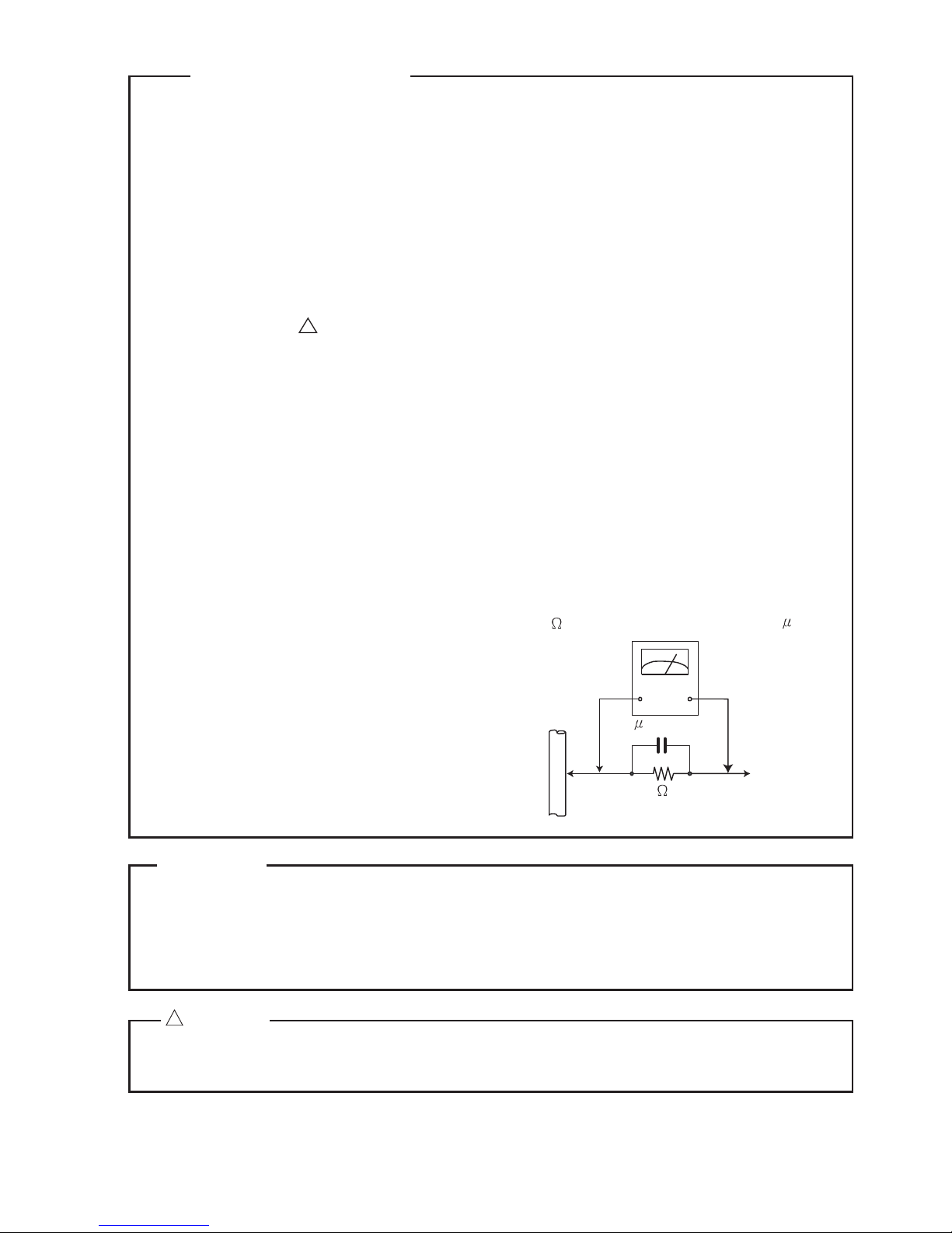
5. Leakage currnet check (Electrical shock hazard testing)
After re-assembling the product, always perform an isolation check on the exposed metal parts of the
product (antenna terminals, knobs, metal cabinet, screw heads, headphone jack, control shafts, etc.)
to be sure the product is safe to operate without danger of electrical shock. Do not use a line isolation
transformer during this check.
Plug the AC line cord directly into the AC outlet. Using a "Leakage Current Tester", measure the
leakage current from each exposed metal parts of the cabinet, particularly any exposed metal part
having a return path to the chassis, to a known good earth ground. Any leakage current must not
exceed 0.5mA AC (r.m.s.)
Alternate check method
Plug the AC line cord directly into the AC outlet. Use an AC voltmeter having, 1,000 ohms per volt or
more sensitivity in the following manner. Connect a 1,500 10W resistor paralleled by a 0.15 F ACtype capacitor between an exposed metal part
and a known good earth ground. Measure the AC
voltage across the resistor with the AC voltmeter.
Move the resistor connection to each exposed
metal part, particularly any exposed metal part
having a return path to the chassis, and meausre
the AC voltage across the resistor. Now, reverse
the plug in the AC outlet and repeat each
measurement. Voltage measured Any must not
exceed 0.75 V AC(r.m.s.). This corresponds to 0.5
mA AC(r.m.s.).
1. This equipment has been designed and manufactured to meet international safety standards.
2. It is the legal responsibility of the repairer to ensure that these safety standards are maintained.
3. Repairs must be made in accordance with the relevant safety standards.
4. It is essential that safety critical components are replaced by approved parts.
5. If mains voltage selector is provided, check setting for local voltage.
Burrs formed during molding may be left over on some parts of the chassis. Therefore,
pay attention to such burrs in the case of preforming repair of this system.
Page 3

Preventing static electricity
1. Grounding to prevent damage by static electricity
Electrostatic discharge (ESD), which occurs when static electricity stored in the body, fabric, etc. is
discharged, can destroy the laser diode in the traverse unit (optical pickup). Take care to prevent this when
performing repairs.
2. About the earth processing for the destruction prevention by static electricity
In the equipment which uses optical pick-up (laser diode), optical pick-up is destroyed by the static electricity
of the work environment.
Be careful to use proper grounding in the area where repairs are being performed.
2-1 Ground the workbench
Ground the workbench by laying conductive material (such as a conductive sheet) or an iron plate over it
before placing the traverse unit (optical pickup) on it.
2-2 Ground yourself
Use an anti-static wrist strap to release any static electricity built up in your body.
3. Handling the optical pickup
1. In order to maintain quality during transport and before installation, both sides of the laser diode on the
replacement optical pickup are shorted. After replacement, return the shorted parts to their original condition.
(Refer to the text.)
2. Do not use a tester to check the condition of the laser diode in the optical pickup. The testers internal power
source can easily destroy the laser diode.
4. Handling the CD changer unit (optical pickup)
1. Do not subject the CD changer unit (optical pickup) to strong shocks, as it is a sensitive, complex unit.
2. Cut off the shorted part of the flexible cable using nippers, etc. after replacing the optical pickup. For specific
details, refer to the replacement procedure in the text.
Remove the anti-static pin when replacing the CD changer
unit. Be careful not to take too long a time when attaching it
to the connector.
3. Handle the flexible cable carefully as it may break when
subjected to strong force.
4. It is not possible to adjust the semi-fixed resistor that
adjusts the laser power. Do not turn it.
Attention when traverse unit is decomposed
*
Please refer to “Disassembly method” in the text for
pick up and how to detach the CD changer mechanism.
1. Remove the CD changer unit.
2. Disconnect the harness from connector on the CD motor
board.
3. Solder is put up before the card wire is removed from connector
Cn601on the main board as shown in Fig.A and Fig. B.
(When the wire is removed without putting up solder, the
CD pick-up assembly might destroy.)
4. Please remove solder after connecting the card wire with
CN601 when you install picking up in the substrate.
Conductive material
(conductive sheet) or iron plate
(caption)
Anti-static wrist strap
Soldering
Fig.B
Flexible cable
Fig.A
CD changer
unit
Page 4

1. CLASS 1 LASER PRODUCT
2. DANGER :
Invisible laser radiation when open and inter
lock failed or defeated. Avoid direct exposure to beam.
3. CAUTION :
There are no serviceable parts inside the
Laser Unit. Do not disassemble the Laser Unit. Replace
the complete Laser Unit if it malfunctions.
4. CAUTION :
The compact disc player uses invisible
laser radiation and is equipped with safety switches
which prevent emission of radiation when the drawer is
open and the safety interlocks have failed or are
defeated. It is dangerous to defeat the safety switches.
Important for laser products
FUSE CAUTION
CAUTION:
REPLACE WITH SAME TYPE
AND RATING FUSE (S).
ATTENTION:
REMPLACER PAR UN(LES)
FUSIBLE(S) DE MEME TYPE
ET DE MEME VALEUR
5. CAUTION : If safety switches malfunction, the laser is able
to function.
6. CAUTION :
Use of controls, adjustments or performance
of procedures other than those specified herein may
result in hazardous radiation exposure.
!
CAUTION Please use enough caution not
to see the beam directly or touch
it in case of an adjustment or
operation check.
Page 5

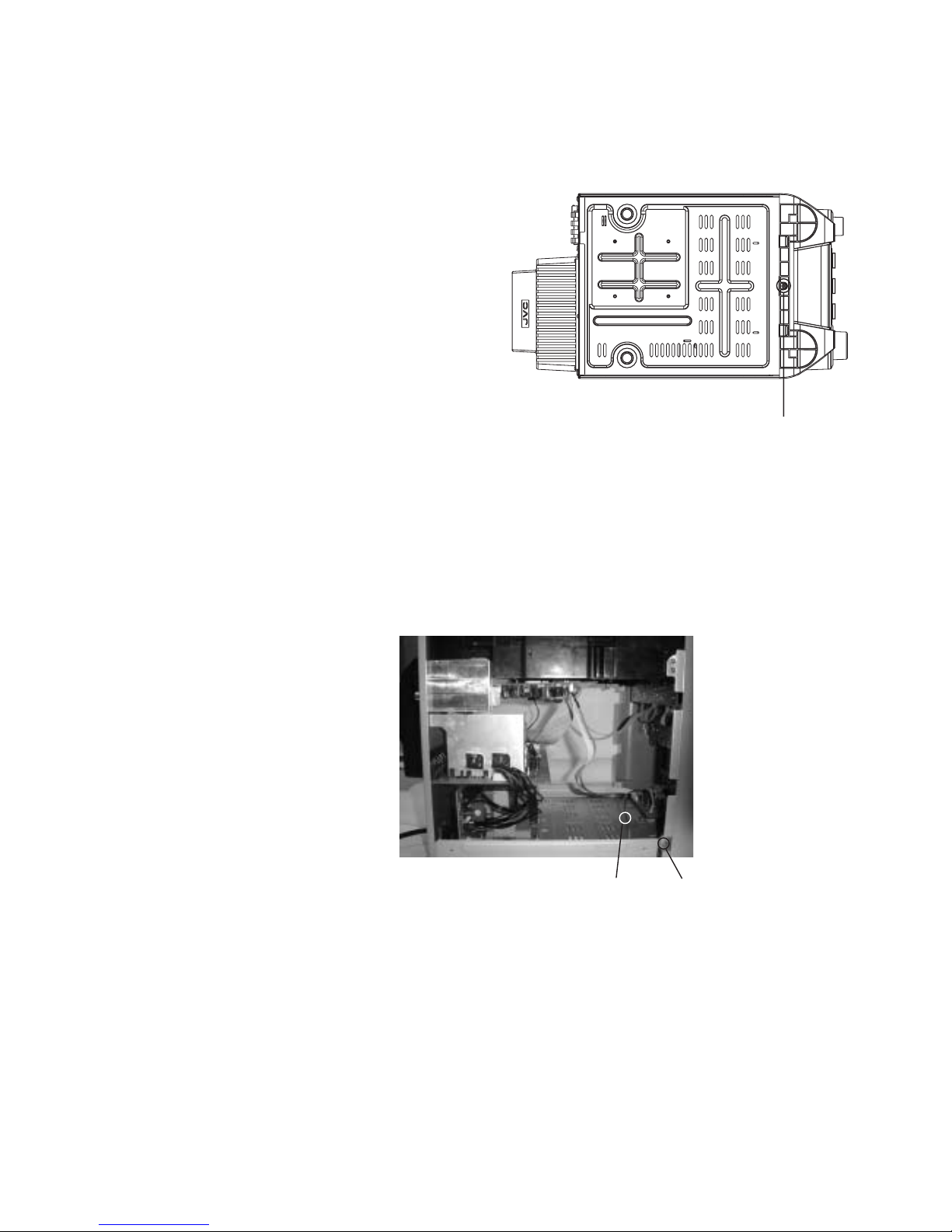
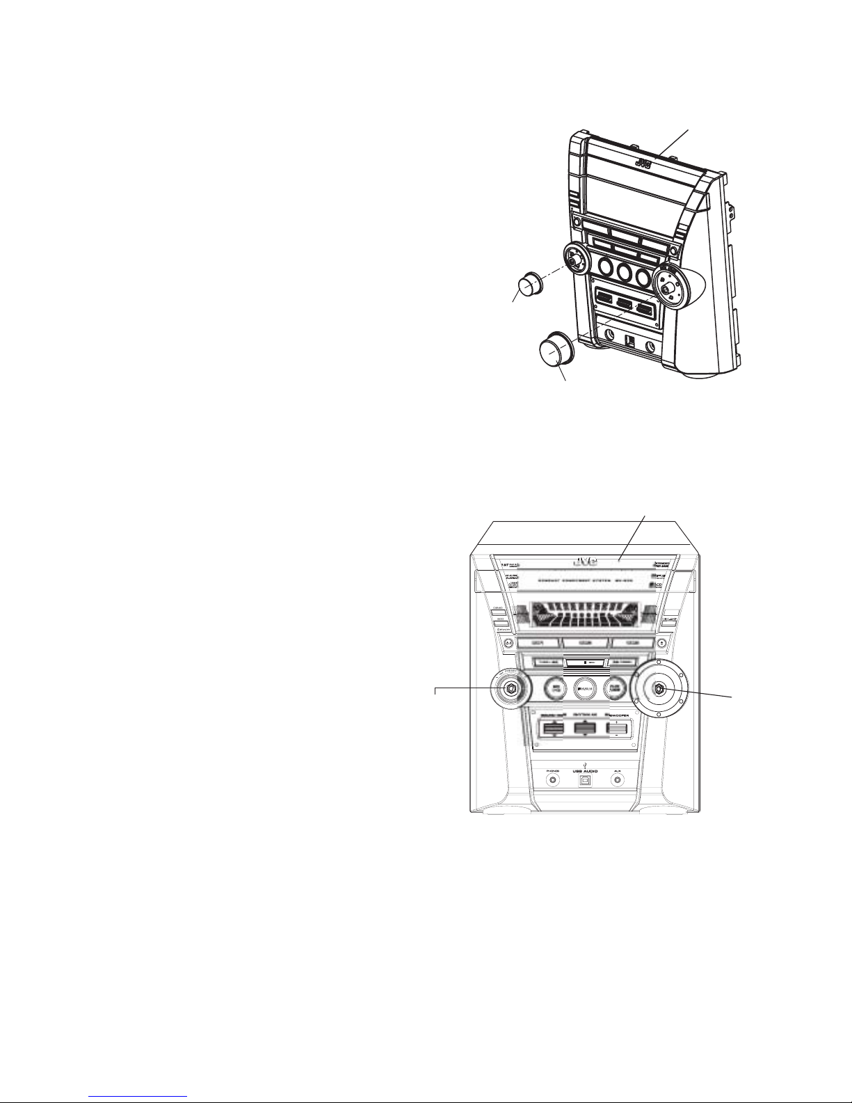
Disassembly method
Commence disassembly of the set by removing the main units and then proceed to the components
and assemblies inside the units.
Replacement of the fuses and the power IC
Top cover
CD changer unit
Front panel assembly
CD changer unit
Removing the main PCB
Removing the CD changer mechanism assembly
Removing the CD pickup
Replacing the loading motor and belt of the CD changer tray
Replacing the CD tray rotor belt of CD changer, and removing the motor
Front panel assembly
Removing the (USB, AUX jack) earphone jack PCB
Removing the control/FL PCB
Removing the volume, preset and CD Function switch PCB
Removing the remote sensor PCB
Removing the standby Led PCB
Removing jack Led backlight PCB
Removing Sound mode PCB
1-5
Page 6
<Disassembly of the main blocks of the set>
Replacement of the fuses and the power IC
Replacing the fuses (See Fig.1)
Prior to performing the following procedure, remove
the left side BOARD.
1. Replace the fuses inside.
[Caution]
Be sure to use fuses with the specified
ratings.
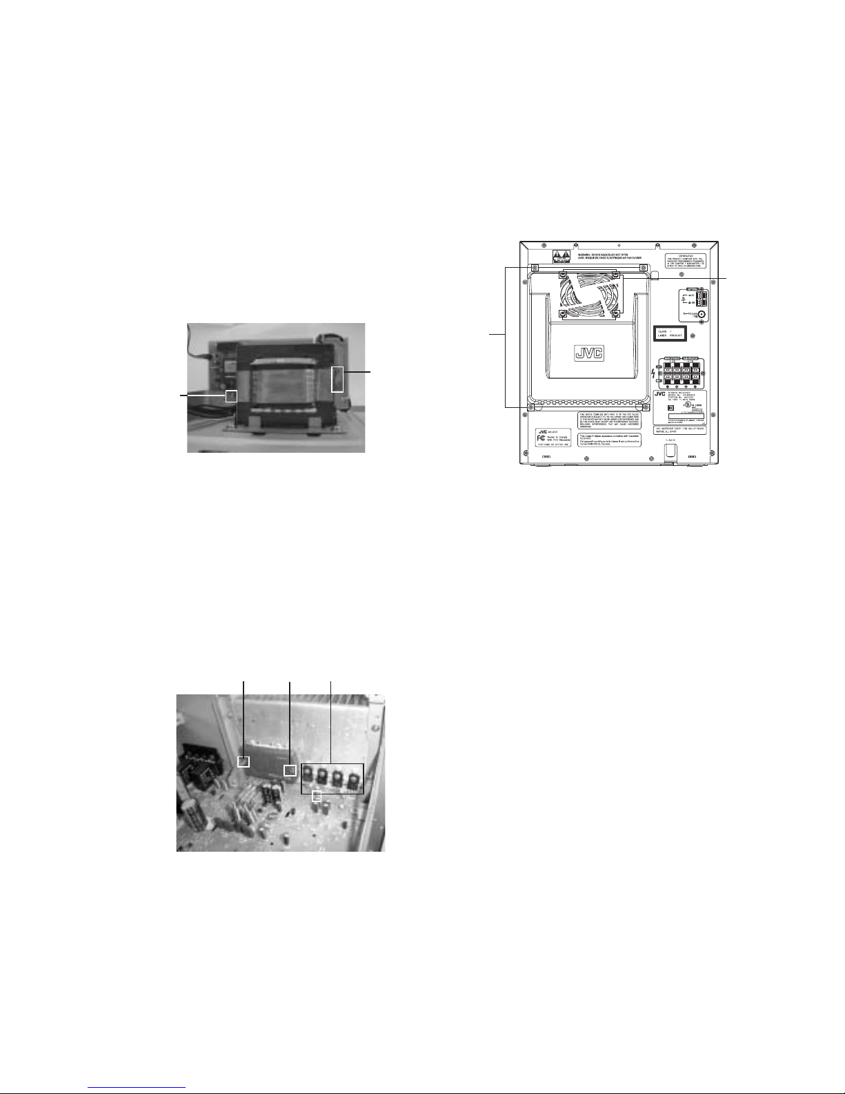
Replacing the heat sink cover (See Fig.3)
1. Remove four screws B from the rear panel.
2. Remove four screws
E
from the heat cover.
3. Pull the heat sink cover outward.
Replacing the power IC (See Fig.2)
Prior to performing the following procedure, remove
the top cover.
1. Remove the two screws A from the heat sink between
the power IC(STK412-430)
2. Remove the four screws B from the heat sink the
between the power IC (D1889,B1340)
3. Remove the solder fixing the power IC.
AA
Fig.2
Fig.1
Fig.3
B
E
Fuse (F901)
3.5A 125V
Fuse (F902)
1.6A 250V
B
Page 7
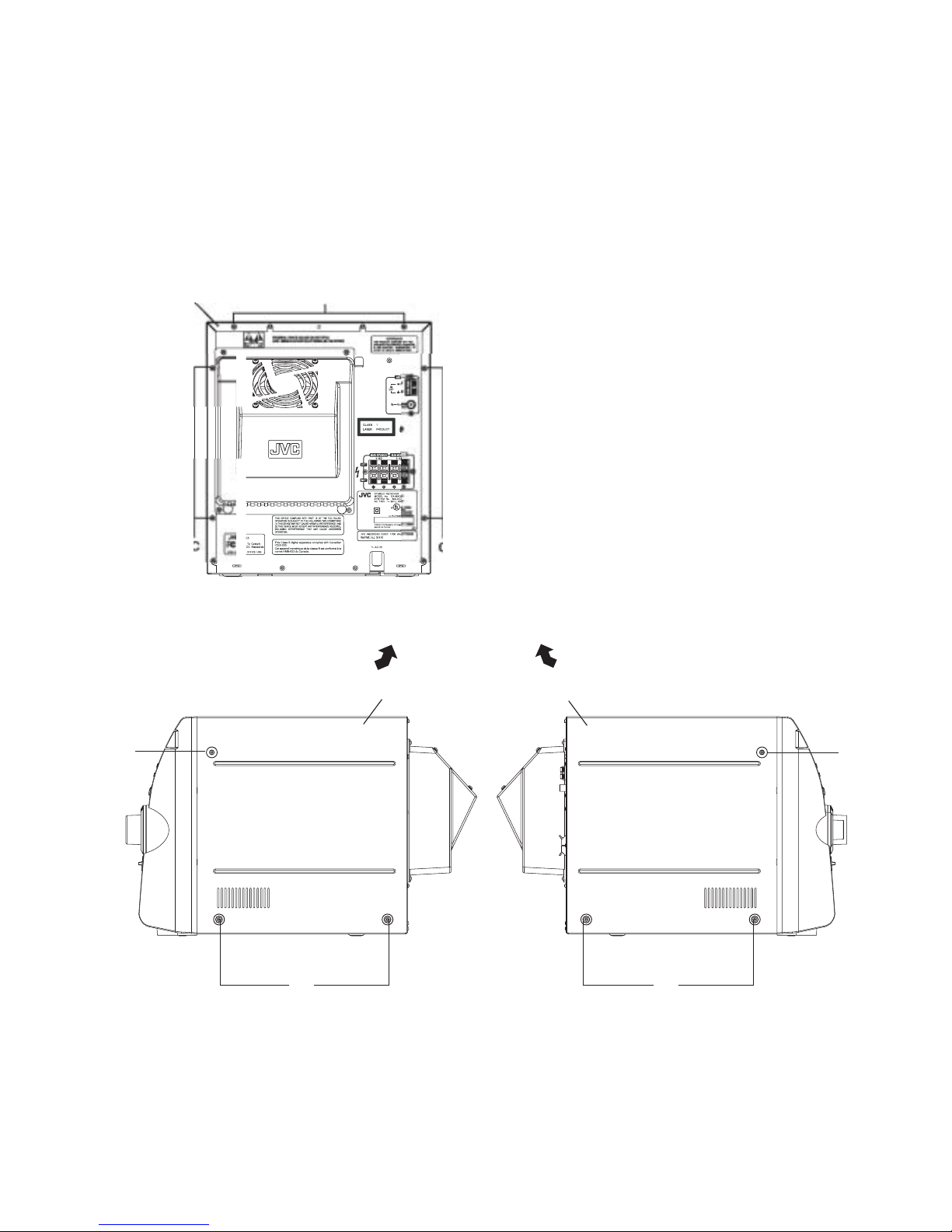
Fig.5
Removing the top cover
(See Fig.4 and 5)
1. Remove six screws C that retain the top cover from
the panel rear of the body.
2.
Remove six screws D that retain the top cover from
the two sides of the body.
3. Remove the top cover from the body by lifting it
toward the rear.
Top cover
C
Fig.4
Right Front panel assembly Left Front panel assembly
D D
D
D
Page 8
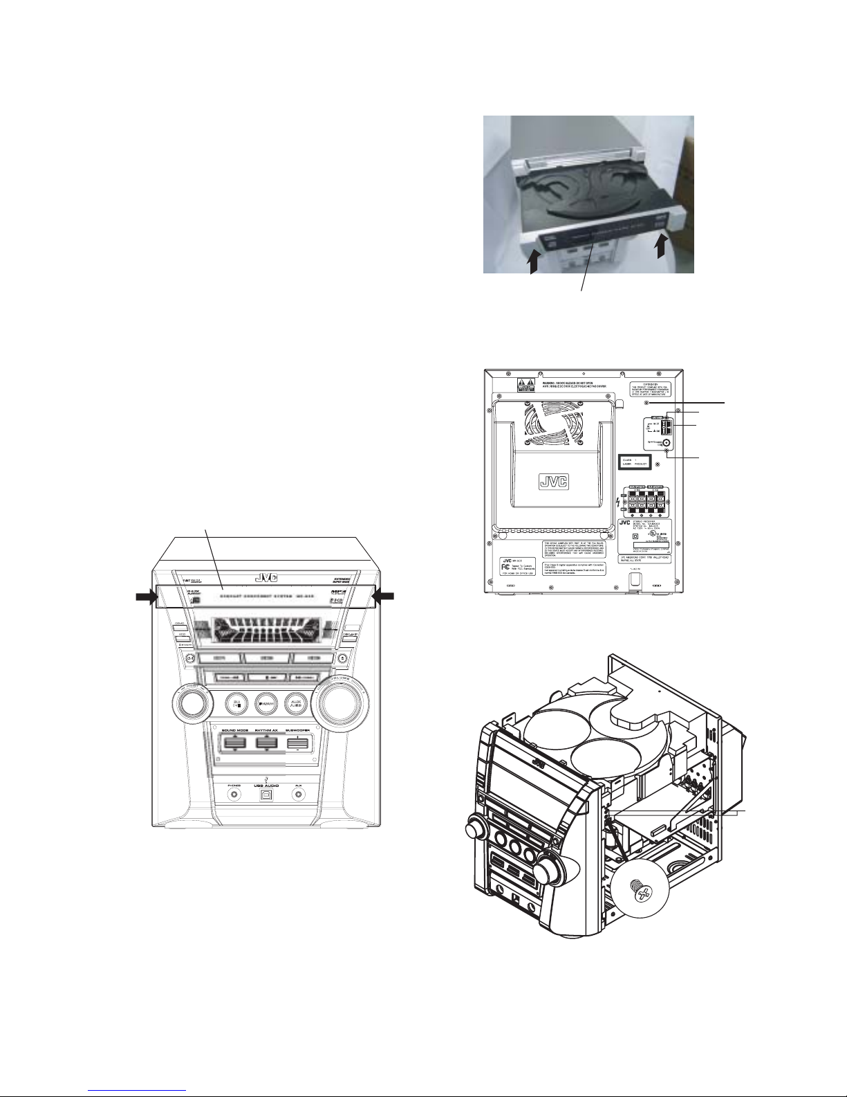
Fig.6
Fig.9
Removing the CD changer unit
(See Fig.6 to 9)
Prior to performing the following procedures, remove
the top cover.
[Caution]
Although the CD mechanism unit can be
removed without removing the CD tray
panel, it is still recommended to remove it
in order to prevent damage.
a. From the front panel side of this set, push in the
sections marked with arrows and pull out the CD
tray toward the front.
b. Remove the CD tray panel by pushing both of
its extremities upward in the direction of the
arrows.
c. Push the CD tray deep into the set.
1.Disconnect the cord wires from the main PCB
CN401,CN601,CN501 and CN203.
2. From the rear of the set, remove two screws E, two
screws F and four screws G on the front panel left
and right side.
3. Handle the CD changer unit rear, take out the unit.
Fig.7
Fig.8
F
E
F
Antenna
terminal
G
CD tray panel
CD tray panel
Page 9
Removing the front panel assembly
(See Fig.10 to 11)
Prior to performing the following procedures, remove
the top cover.
Also remove the CD changer unit.
1. Disconnect the parallel wire and the cord wire from
the connectors CN201, CN401 on the main PCB.
2. Remove one screws H retaining the front panel
assembly onto the bottom of the body.
3. Remove two screws I on the left and right side of the set
retaining the panel front from the bottom and then
remove then GND lug b that comes from the power
amp and supply PCB.
4. Disengage the claws c on both sides of the front
panel assembly and then remove the assembly.
Fig.10
H
Fig.11
Claw
c
GND lug
b
Page 10
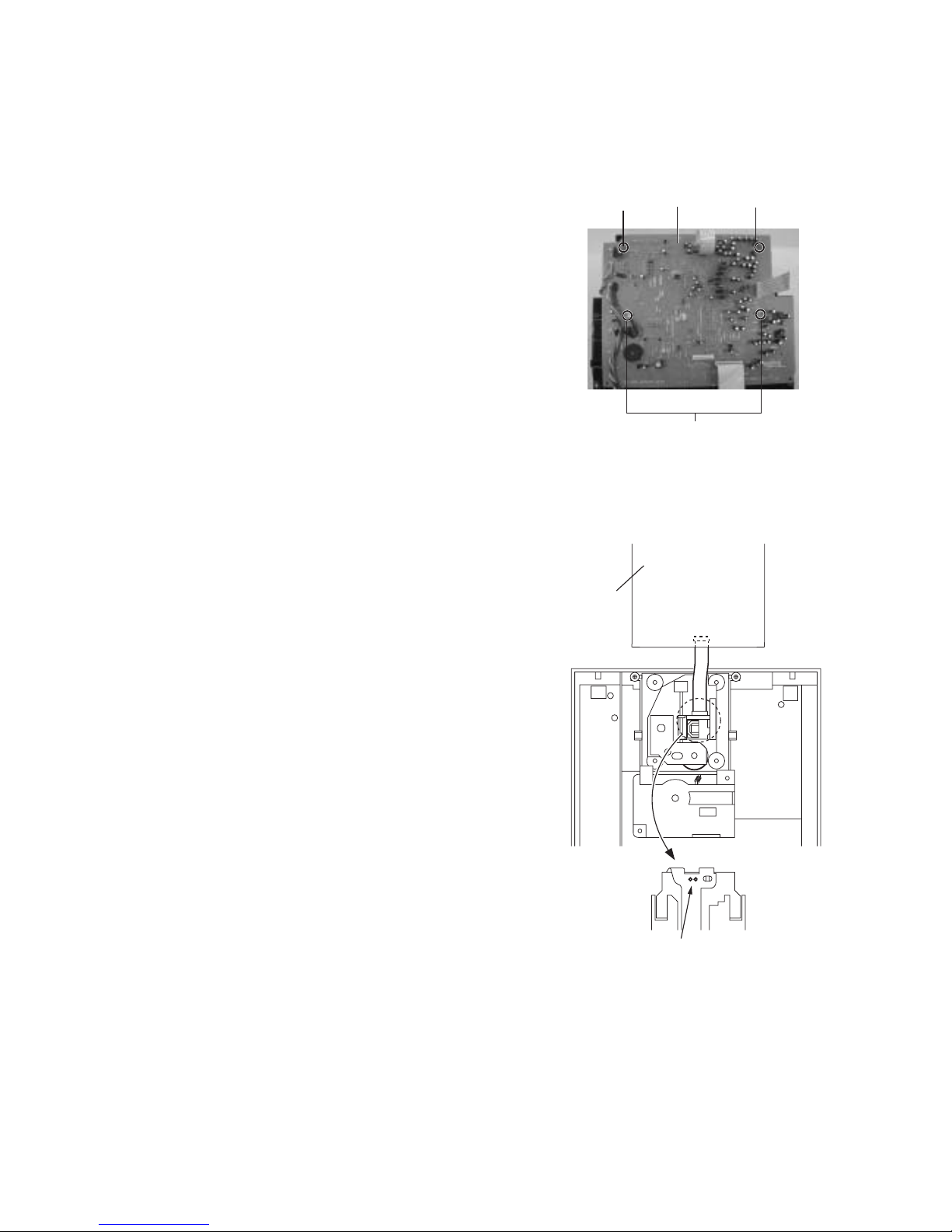
Fig.13
CD PCB
Short round
CN601
Fig.12
<Disassembly of units and assembly
inside this set>
Removing the MAIN PCB
(See Fig.12 to 13)
Prior to performing the following procedures, remove
the top cover.
Also remove the CD changer unit.
1. Disconnect the wires from CN701, CN702 and
CN703 on the CD PACK PCB, which is located on
the down side of the CD changer unit.
2. The four screws J that retain the CD PCB should
be removed.
3. Remove the CD PCB by pulling it toward the side
where the CN701 is located.
4. Using solder, short the CD pickup to connect to
short round.
[Caution]
After re-connecting the wires, be sure to
remove the shorting solder from the GND
connection.
5. Disconnect the card wire from the connector CN701
on the main PCB and then remove the main PCB.
J
CD PCB
J
J
Page 11

Fig.14
Fig.15
assemb
ly
e
( Green color )
e
( Red color )
e
( Green color )
e
( Red color )
d
CD changer
unit
Removing the CD changer mechanism
assembly (See Fig.14 to 15)
Prior to performing the following procedures, remove
the top cover.
Also remove the CD changer unit.
1. Turn the CD changer mechanism cover base and
remove the screws d connecting the unit to the CD
changer mechanism assembly.
2. Removing four screws e retaining the CD mechanism
holder assembly.
[Caution]
When replacing the CD changer mechanism
assembly, be sure not to mistake the positions
of the silver color and copper color spring.
CD changer
mechanism
Page 12
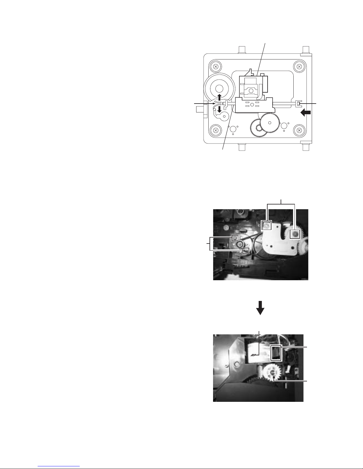
Fig.16
Fig.17
Fig.18
Motor locker
Turn table motor
Obligue gear
, and then remove the CD tray
g
M
L
f
CD pickup
Shaft
Removing the CD pickup (See Fig.16)
Prior to performing the following procedures, remove
the top cover.
Also remove the CD changer unit.
Also remove the CD changer mechanism.
1. Widen the section
f
.
2. While keeping the section f wide open, push the
section g in the direction of the arrow to remove
the shaft, and then remove the CD pickup.
Replacing the loading motor and rotor
belt of the CD changer (See Fig .17)
Prior to performing the following procedures, remove
the top cover.
Also open the CD changer tray.
1. Remove the two screws L retaining the CD changer
tray loading motor.
2. Remove the two screws M retaining the gear plate
and take it out, after remove the rotor belt from the
pulley.
Replacing the CD turn table and removing the motor (See Fig. 18 )
Prior to performing the following procedures, remove
the top cover.
Also remove the CD changer unit.
1. Remove the one screws
N
retaining the CD (Turn
table).
2. Remove the two screws O retaining the stopper
brackets on both sides of the CD changer unit.
3. Remove the stopper brackets from both sides of
the CD changer unit.
4. Pull out the CD tray from the CD changer unit, all
the way and lift the tray (u/~ ward) to remove.
5. Remove the gear and after push out the tray motor
locker and pull out the tray motor from the CD tray.
Page 13
Fig.20
Fig.19
S
Q
R( 17PCS)
T
Z
P
L
Front panel
assembly
Remote sensor
PCB
Standby Led
PCB
Fig.21
Removing the USB,AUX,earphone PCB
(See Fig.19)
Prior to performing the following procedures, remove
the top cover.
Also remove the CD changer unit.
Also remove the front panel assembly.
Remove six screws
Z
retaining the USB,AUX,
earphone PCB.
Removing the remote sensor PCB & the
standby PCB
(See Fig.20)
Prior to performing the following procedures, remove
the top cover.
Also remove the CD changer unit.
Also remove the front panel assembly.
1. Remove four screws
P
that retains the
remote sensor PCB.
2. Remove four screws
L
that retains the
standby Led PCB.
Removing the display PCB
(See Fig.21)
Prior to performing the following procedures, remove
the top cover.
Also remove the CD changer unit.
Also remove the front panel assembly.
1. Remove four screws Q that retain the display PCB
from the back of the front panel unit.
Q
Q
Front panel
assembly
Display PCB
Page 14
Removing sound mode and volume , pre-
set and CD function switch PCB
(See Fig.20 to 23)
Prior to performing the following procedures, remove
the top cover.
Also remove the CD changer unit.
Also remove the front panel assembly.
1. Pull out the volume control knob from the front of
the front panel assembly.(Fig.22)
2. Pull out the preset knob from the front of the front
panel assembly (Fig.22)
3. Remove four screws Q retaining the front panel
assembly.
4. Remove the control/FL PCB.
5. Remove eight screws S retaining the sound mode
switch PCB.(Fig.21)
6. Remove seventeen screws R retaining the volume ,
preset and CD founction switch PCB.(Fig.20)
7. Remove two screws T retaining the jack Led
Backlight PCB.
Fig.22
Fig.23
Volume knob
Preset Knob
Preset shaft
Front panel
assembly
Volume
shaft
Front panel assembly
Page 15
Fig.28
Fig.31
Rear panel
Power amp and
supply PCB
Z(4PCS)
Fig.29
Removing the bridge diode
(See D214, D215 and Fig.28)
Prior to performing the following procedures, remove
the top cover and both sides board.
1. Remove two screws W that connect the heat sink.
2. Remove the solder fixing the 4-pin bridge diode
(D214, D215).
Removing the power amp and supply PCB
and the power trans PCB
(See Fig. 2, 29 to 31)
Prior to performing the following procedures, remove
the top cover and CD changer unit.
1. Remove four screws B from the rear panel. (Fig.3)
2. Pull the heat sink cover outward.
3. Remove four screws
AA
from the rear panel between
the heat sink holder.
4. Remove four screws
YY
that retains the rear panel,
and then remove the rear panel.
5. Disconnect the parallel wires from the connectors
FW951 on the power trans PCB.
6. Remove screws Z that retain the power amp and
supply PCB and then remove the assembly.
7. Remove four screws that retain the power trans PCB
and then remove the assembly.
Fig.30
YY
Clamp
AA
Fuse (F901)
3.5A 125V
Fuse (F902)
1.6A 250V
W
Page 16
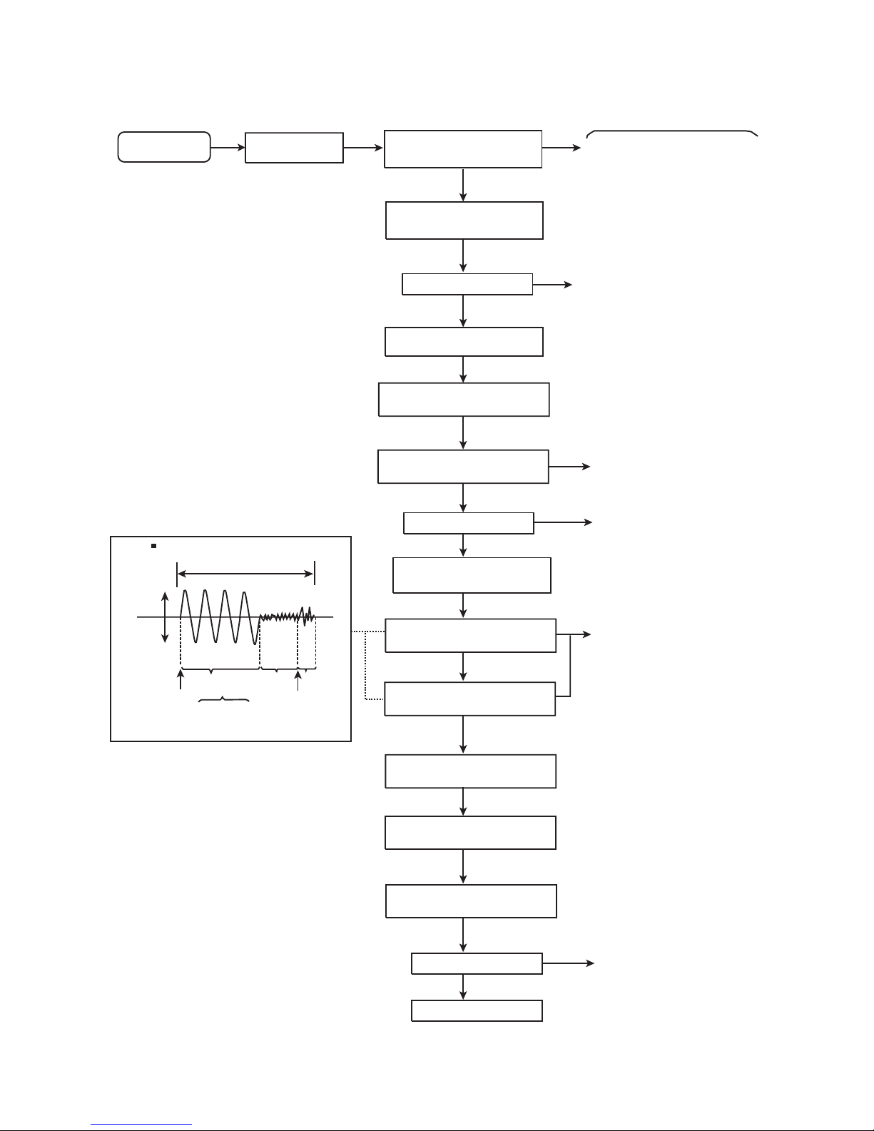
Flow of functional operation until TOC read
Slider turns REST
SW ON.
Automatic tuning
of TE offset
Laser ON
Detection of disc
Automatic measurement of
Focus S-curve amplitude
Automatic tuning of
Focus offset
Disc is rotated
Focus servo ON
(Tracking servo ON)
Automatic tuning of
Tracking error balance
Automatic measurement of
Tracking error amplitude
Automatic tuning of
Focus error balance
Disc to be
braked to stop
Tracking
servo
on states
Tracking
servo
off states
Disc states
to rotate
TOC reading
finishes
Automatic measurement
of TE amplitude and
automatic tuning of
TE balance
500mv/div
2ms/div
Fig-1
Approx.3sec
pin 20 of
IC611(TE)
Approx
0.3V
VREF
Tracking error waveform at TOC reading
Power ON
Play Key
Confirm that the Focus error
S-cuve signal at the pin31 of
IC701 is approx.2Vp-p
Confirm that the signal from
pin26 IC701 is 0V as a
accelerated pulse during
approx.400ms.
Confirm the waveform of
the Tracking error signal.
at the pin 29 of IC701 (R729)
(See fig-1)
Automatic tuning of
Focus error gain
Automatic tuning of
Tracking error gain
TOC reading
Play a disc
Confirm the eys-pattern
at the lead of Pin 2 of IC 701
Confirm that the voltage at the pin5
of CN702 is "H"\"L"\"H".
Check Point
Check that the voltage at the
pin10 of IC701 is + 0V?
Page 17
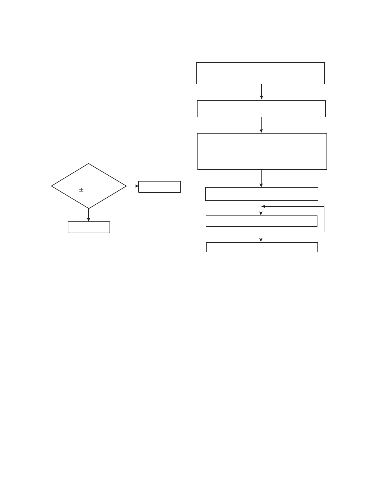
Turn off the power switch and,disconnect the
power cord from the AC OUTLET.
Replace the pickup with a normal one.(Refer
to "Pickup Removal" on the previous page)
Plug the power cord in,and turn the power on.
At this time,check that the laser emits for
about 3seconds and the objective lens moves
up and down.
Note: Do not observe the laser beam directly.
Play a disc.
Check the eye-pattern at
Pin 2 of IC 701
Finish.
Maintenance of laser pickup
Is the level of
RFOUT under
0.48V 0.1Vp-p?
Replace it.
NO
YES
O.K
Replacement of laser pickup
(1) Cleaning the pick up lens
Before you replace the pick up, please try to clean
the lens with a alcohol soaked cotton swab.
(2) Life of the laser diode
When the life of the laser diode has expired, the
following symptoms will appear.
1. The level of RF output (EFM output : ampli tude of
eye pattern) will below.
(3) Semi-fixed resistor on the APC PC board
The semi-fixed resistor on the APC printed circuit board which is attached to the pickup is used to adjust the
laser power.Since this adjustment should be performed to match the characteristics of the whole optical
block, do not touch the semi-fixed resistor.
If the laser power is lower than the specified value, the laser diode is almost worn out, and the laser pickup
should be replaced.
If the semi-fixed resistor would be adjusted when the pickup operates normally, the laser pickup may be
damaged due to excessive current.
Page 18
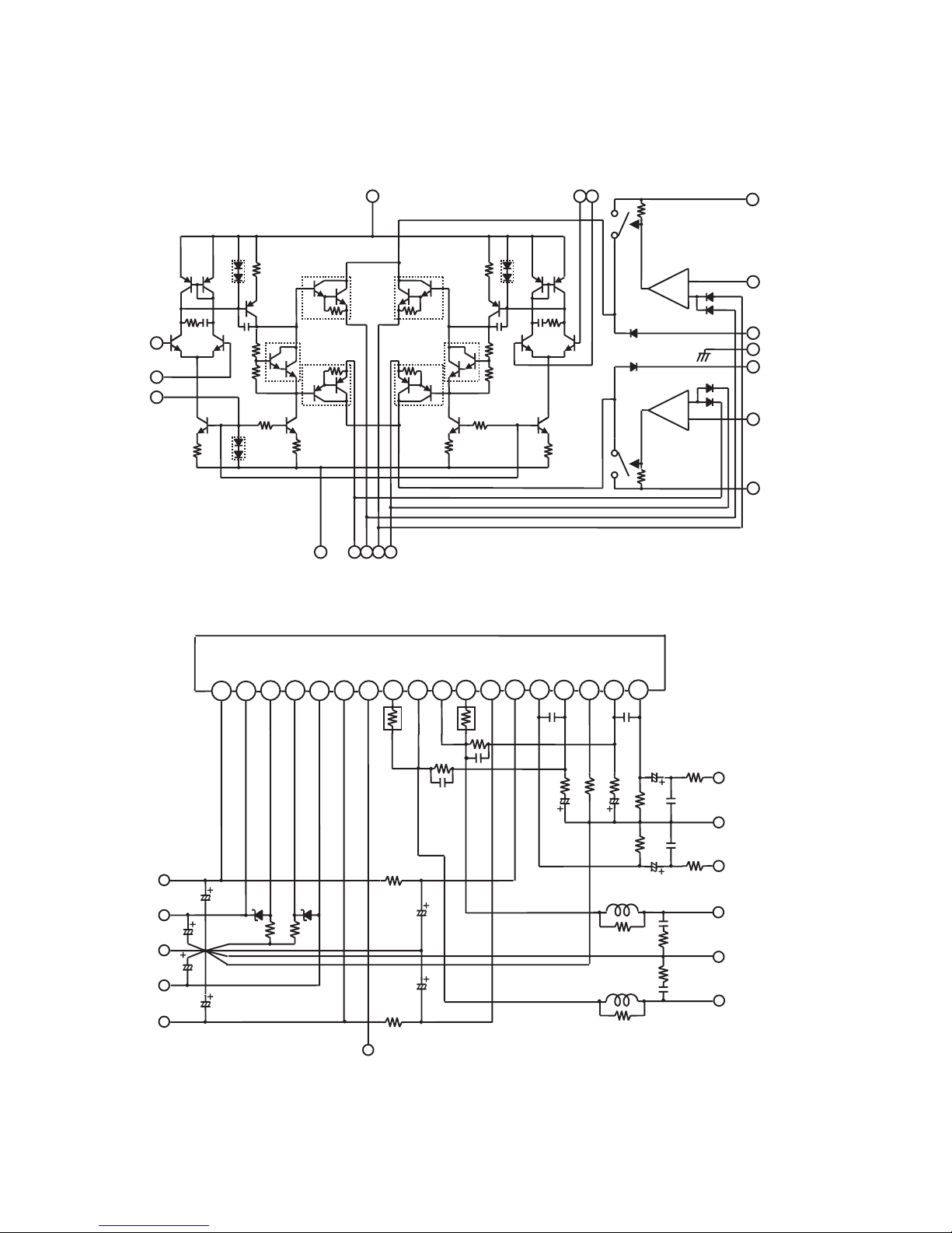
Description of major ICs STK412-430 (IC201) : Dual low noise operational
1. Equivalent Block Diagram
2. Test Circuit
(*1)Metal Plate Cement Resistor 0.22ohm+-10%(5W)
SUB.GND
1
2 3 4
5
6
7
891011 12
13
14
17
18 15
16
+VH
+VL
GND
-VL
-VH
GND
Ch1 OUT
GND
Ch1 IN
Ch2 IN
GZA
1
X
GZA
1
X
1.5kohm
/1
W
1.5kohm
/1
W
100uF
/100V
100uF
/50V
100uF
/50V
100u
F
/100V
100u
F
/100V
100uF
/100V
100ohm/1
W
100ohm/1
W
*1
*1
56kohm
56kohm
100p
F
100p
F
3p
F
3p
F
56
0
ohm
56
0
ohm
33kohm
100uF
/10V
100u
F
/10V
56kohm 56kohm
47
0
p
F
470p
F
2.2uF
/50V
2.2uF
/50V
1kohm
1kohm
3uH
3uH
Ch2 OUT
4.7ohm
4.7ohm
4.7ohm/1
W
4.7ohm/1
W
0.1u
F
0.1u
F
TR41
TR51
R41
R51
D
4
D
5
D
5
D52
Comparato
r
Comparato
r
1
5
1
4
9
11
1
0
8
1
2
1
8
6
5
2
1
4
3
1
7
TR1
TR2
TR
3
TR
4
TR
5
TR
6
TR7
TR8
TR9
TR10
TR11TR12
TR1
3
TR1
4
TR1
5
TR1
6
TR17
TR18
TR19
TR20
D1
R1
R2
R
3
R
4
R
5
R
6
R7
R11
R12
R1
3
R1
4
R1
5R16
R17
C1
C2 C11
C12
D2
D12
SUB
Page 19
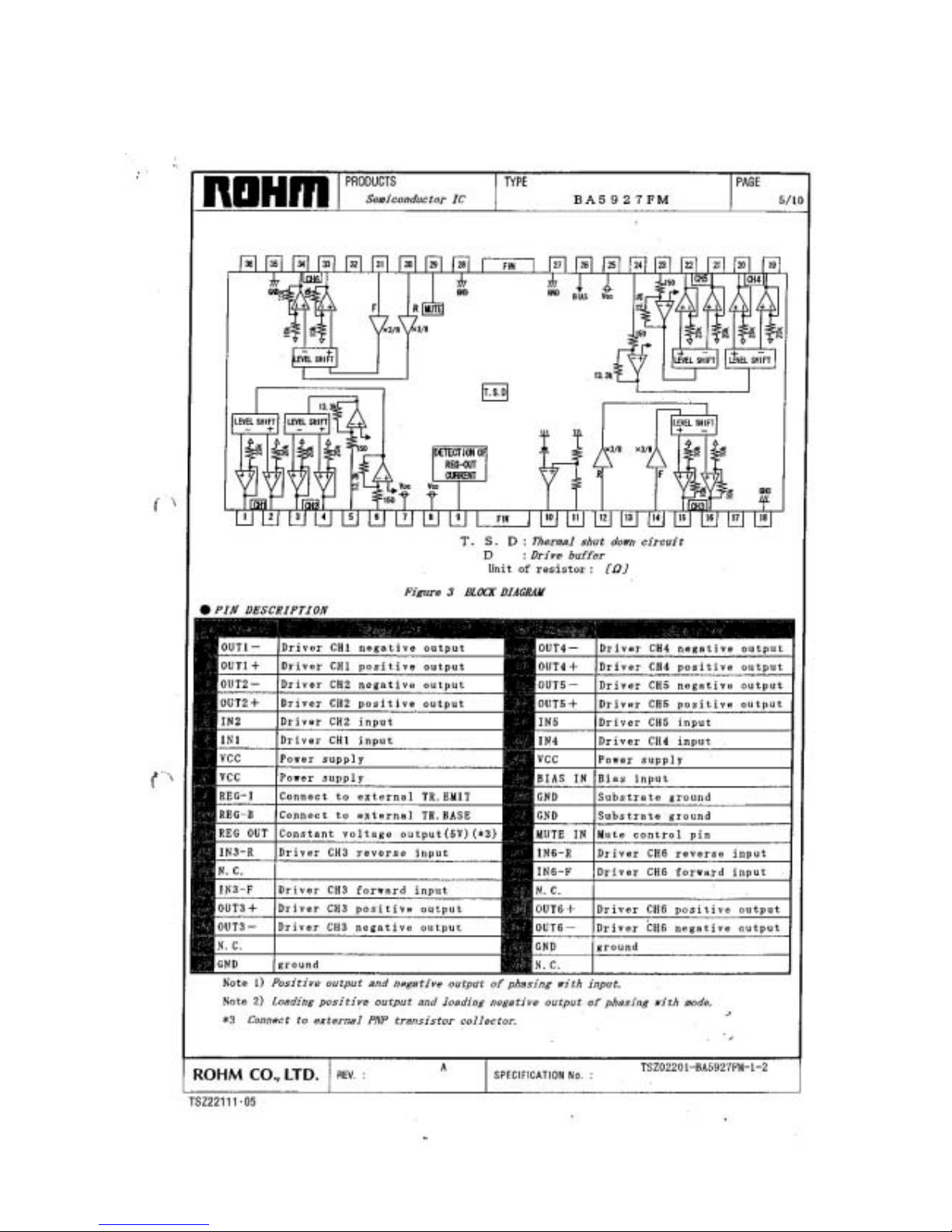
CD DRIVE ICS BA5927FM(IC702)
Page 20
1. Terminal layout
-+
+-
OUT1
- IN1
+IN1
VEE
Vcc
OUT2
- IN2
+IN2
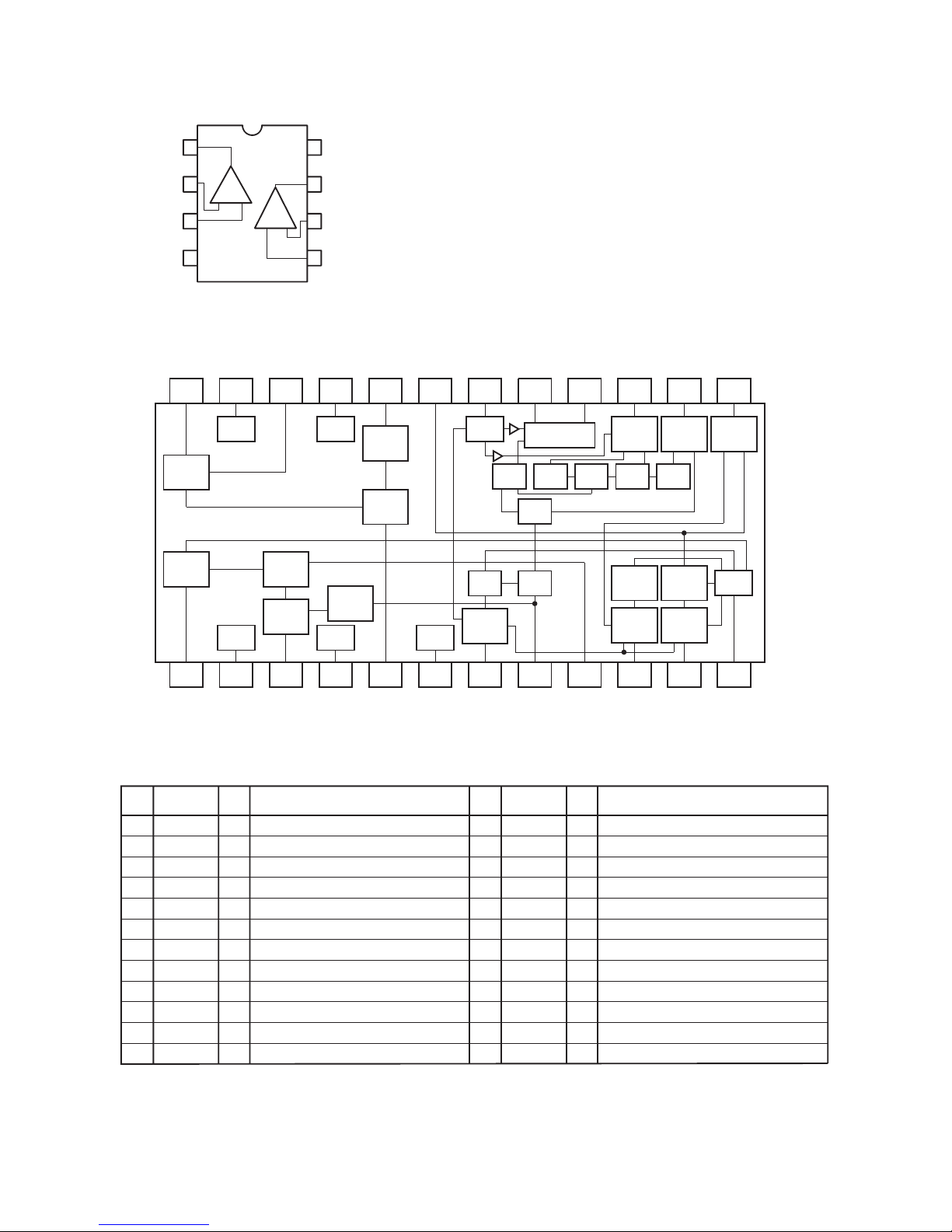
BA4558F (IC503) : Dual low noise operational amp.
1chip AM/FM, MPX tuner system
Pin
No.
Symbol
Function
I/O
Pin
No.
Symbol
Function
I/O
2. Pin function
1. Block diagram
1 AM_RFIN I AMRF signal input
2 REG. -
3 AM_OSC - AM local oscillation circuit
4 VCC_1 - Power supply terminal
5
FM_MIXOUT
O Output terminal for FM mixer
6 GND_1 - Ground
7
IF_BUFFER
O IF buffer output
8 ST_IND O Stereo indicator output
9
AM_MIXOUT
O Output terminal for AM mixer
10 FM_IF IN I Input of FMIF signal
11 AM_IF IN I Input of AMIF signal
12 AGC I AGC voltage input terminal
13 FM_DET O FM detection signal output
14
ST/MON_SW
I Stereo/Monaural switching signal input
15
AM/FM_SW
I AM/FM switching signal input
16 L_OUT O Output L-channel
17 R_OUT O Output R-channel
18 MPX_IN I Multiplex signal input
19 DET_OUT O AM/FM detection output
20 FM_OSC - FM local oscillation circuit
21 VCC_2 - Power supply terminal
22
FM_RFOUT
O Output of FMRF signal
23 GND_2 - Ground
24 FM_RFIN I Input of FMRF signal
24
FM
RF
FM
OSC
23
GND2
21
VCC2
20
FM
MIX
PHASE
COMP
15
PILOT
DET
14
FM
DET
1319 18
MUTE
17 16
DECODER
22
1 2 4 5 10 11 126 7 8 93
ST SW
FM
S-METERAMDET
VCO FF FF
TRIG
STSD
FF
AGC
FM
IF
AM
IF
AM
RF
REG VCC1 GND1
AM
MIX
AM
OSC
OSC
BUFFER
IF
BUFFER
1. Pin descriptions
Page 21
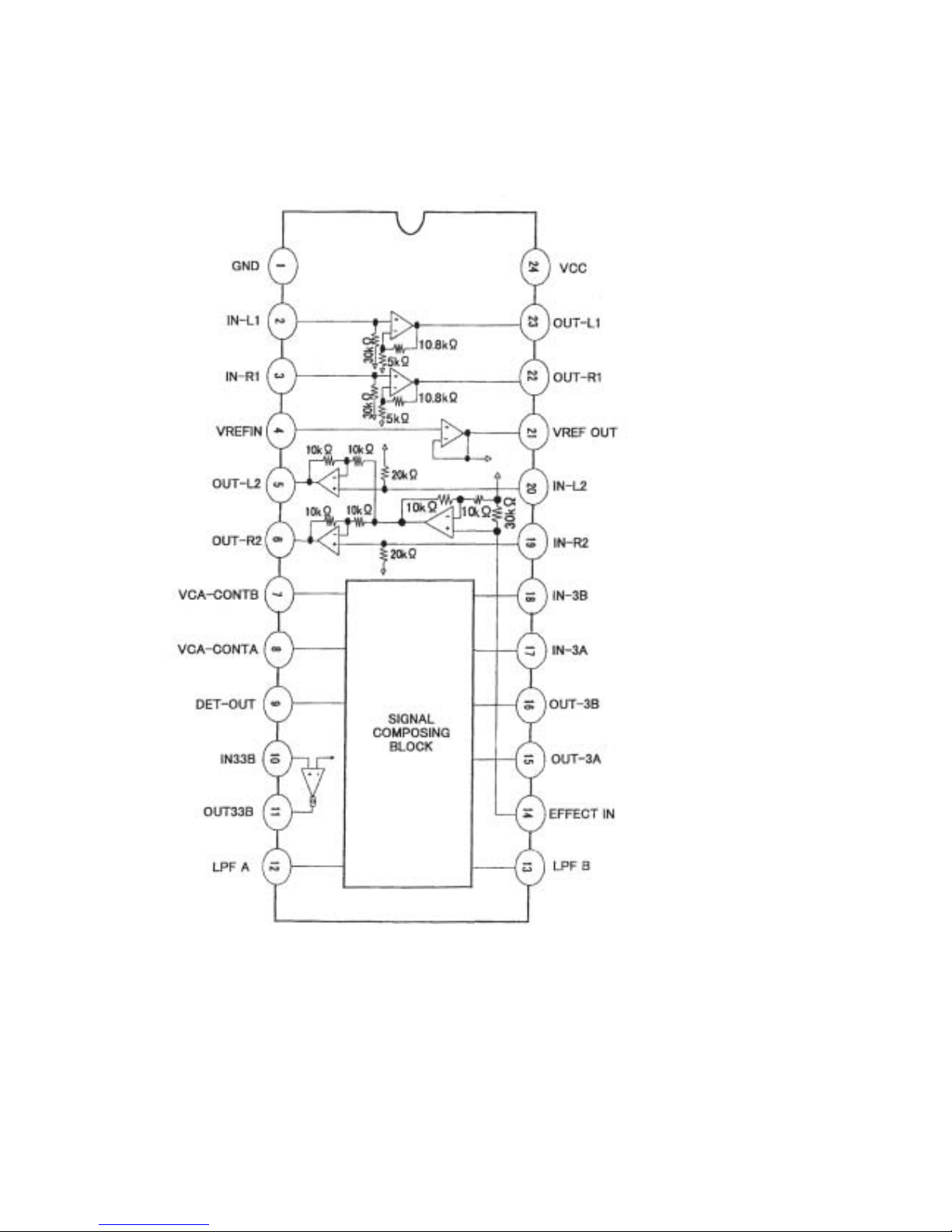
RHYTHM AX (IC502) JCV8011 : Block diagram
Page 22

1. Application diagram
RF AMP & SERVO SIGNAL PROCESSOR (IC701): S1L9226X
S1L9226X
To Micom
From Micom
TEO
TEM
SLP
SLO
SLM
ISTAT
MCK
MDATA
MLT
RESET
WDCK
CLVI
LOCK
ASY
EFM
SPM
EFMI
VCC
FRSH
FSET
FLB
FGD
FSI
TGU
EQO
EQI
RFO
RFM
PD
LD
37
38
39
40
41
42
43
44
45
46
47
48
24
23
22
21
20
19
18
17
16
15
14
13
1 2 3 4 5 6 7 8 9 10 11 12
36 35 34 33 32 31 30 29 28 27 26 25
Pick-up
LD
PD
A
C
B
D
F
E
VR
VCC
GND
55k
55k
55k
55k
82k
82k
103
103
333
683
33
F
2pF
22k
682
821
47
F
430k
104
104
102
104
10k
From Micom
From Micom
From Micom
474
333
SMEF
8.2k
20k
SMDS
SMDP
10k
From DSP
From DSP
to DSP
474
103
10k
100k
88k
103
22k
683
47k
10
F
120k
39k
104
100k120k
391
222
from pick-up
150k
104
333
100k
104
47
F220
100 F
SPO
FEM
FEO
GND
TZC/SSTOP
TEIO
LPFT
ATSC
PDAC
PDF
PDBD
PDE
DCB
MCP
DCCI
DCCO
VREF
EQC
272
10k
1M
104
2pF
Page 23

4
12
RF AGC & EQ
Control
Focus OK Detect
Defect Detect Mirror
Gen
Center
Voltage
APC. Laser
Control &
LPC
Tracking Servo Loop
- Gain & Phase
Compensation
- Track Jump
- Offset Adjust
- TZC Gen.
Tracking Error
(RW)
I/V AMP
RF & Focus
Error (CD-RW)
I/V AMP
Hardware Logic
- Auto-Sequencer
- Fast Search
- Febias, Focus Servo,
Tracking Offset ADJ.
- Tracking Balance & Gain
Adjust
- Interruption Detect
- EFM Muting System
Sled Servo &
Kick Gen
Spindle
Servo LPF
EFM
Comparator
Micom Data Interface Logic Decoder
Focus Servo Loop
- Gain & Phase
Compensation
- Focus Search
- Offset Adjust
- FZC Gen.
EQO
PD
LD
LPFT
TEIO
TZC&
SSTOP
ATSC
TEO
TEM
SLP
SLO
SLM
FEO
FEM
SPDLO
SPDLM
EQI
RFO
RFM
EQC
VREF
PDE
PDF
PDBD
PDAC
ISTAT
MCK
MDATA
MLT
RESET
WDCK
CLVI
LOCK
ASY
EFM
5
45
46
44
43
6
7
8
9
10
11
1413 15 16 17 19 18 20 22 21
24
23
30
29
25
26
27
28
29
36
33
34
35
37
38
39
41 40424748123
EFMI
DCCI
DCC0
MCP
DCB
VCC/
VDD
FRSH
FSET
FLB
FGD
FSI
TGU
2. Block diagram
Page 24

Table 1. Pin Description
Pin No. Symbol I/O Description
1 RFM I RF summing amp. inverting input
2 RFO O RF summing amp. output
3 EQI I RFO DC eliminating input(use by MIRROR, FOK ,AGC & EQ terminal)
4 EQO O RF equalizer output
5 EFMI I EFM slice input. (input impedance 47K)
6 VCC P Main power supply
7 FRSH I Capcitor connection to focus search
8 FSET I Filter bias for focus,tracking,spindle
9 FLB I Capacitor connection to make focus loop rising band
10 FGD I Terminal to change the hign frequency gain of focus loop
11 FSI I Focus servo input
12 TGU I Connect the component to change the high frequency of tracking Loop
13 ISTAT O Internal status output
14 MCK I Micom clock
15 MDATA I Data input
16 MLT I Data latch input
17 RESET I Reset input
18 CLVI I Input the spindle control output from DSP
19 WDCK I 88.2KHz input terminal from DSP
20 LOCK I Sled run away inhibit pin (L: sled off & tracking gain up)
21 EFM O EFM output for RFO slice(to DSP)
22 ASY I Auto asymmetry control input
23 SPM I Spindle amp. inverting input
24 SPO O Spindle amp. output
25 SLM I Sled servo inverting input
26 SLO O Sled servo output
27 SLP I Sled servo noninverting input
28 TEM I Tracking servo amp.inverting input
29 TEO O Tracking servo amp. output
30 FEM I Focus servo amp. inverting input
31 FEO O Focus servo amp. output pin
3. Pin description
Page 25

32 GND P Main ground
33 TZC/
SSTOP
I Tracking zero crossing input & Check the position of pick-up
wherther inside or
not
34 TEIO B Tracking error output & Tracking servo input
35 LPFT I Tracking error integration input (to automatic control)
36 ATSC I Anti-shock input
37 LD O APC amp. output
38 PD I APC amp. input
39 PDAC I Photo diode A & C RF I/V amp. inverting input
40 PDBD I Photo diode B & D RF I/V amp. inverting input
41 PDF I Photo diode F & tracking(F) I/V amp. inverting input
42 PDE I Photo diode E & tracking(E) I/V amp. inverting input
43 DCB I Capacitor connection to limit the defect detection
44 MCP I Capacitor connection to mirror hold
45 DCCI O Output pin to connect the component for defect detect
46 DCCO I Input pin to connect the component for defect detect
47 VREF O (VCC+GND)/2 Voltage reference output
48 EQC I AGC_equalize level control terminal & capacitor terminal to input in to VCA
Item Symbol Rating Unit
Power supply voltage V
DD
2.7 3.3 V
Absolute Ratings V
I
4.5 V
Operating temperature T
OPR
-20 75 °C
Storage temperature T
STG
-40 125 °C
Table 1. Pin Description (Continued)
Pin No. Symbol I/O Description
Page 26

4. Maximum absolute ratings
5. Electrical characteristics
Table 2. Electrical Characteristics
No. Characteristics Symbols Test Block
Spec
Unit
Min. Typ. Max.
1
Supply current 2.7V ICCTY 5 10 20 mA
2 RF AMP offset voltage Vrfo RF AMP -100 0 100 mV
3 RF AMP offset voltage 2 Vrfo2 -300 -200 -100 mV
4 RF AMP oscillation voltage Vrfosc 0 50 100 mV
5
RF AMP voltage gain AC Grf 15.5 18.5 23.5 dB
6
RF THD characteristic Rfthd - - 5 %
7
RF AMP maximum output voltage Vrfh 2.35 - - V
8 RF AMP minimum output voltage Vrfl - - 0.85 V
9 RF CDRW gain AC1 GRWAC1 1.05 1.30 1.55 -
10 RF CDRW gain AC2 GRWAC2 1.05 1.30 1.55 -
11
RF CDRW gain AC3 GRWAC3 1.05 1.30 1.55 -
12
Focus error offset voltage VFEO1
Focus Error
-525 -250 0 mV
13
Focus error auto voltage VFEO2 -50 0 50 mV
14 ISTAT state after FEBIAS control VISTAT1 2.2 - - V
15 Focus positive offset 1 Vfep1 0 40 80 mV
16 Focus positive offset 2 Vfep2 10 60 100 mV
17
Focus positive offset 3 Vfep3 50 120 180 mV
18
Focus negative offset 1 Vfen1 -80 -40 0 mV
19
Focus negative offset 2 Vfen2 -100 -60 -10 mV
20 Focus negative offset 3 Vfen3 -180 -120 -50 mV
21 Focus Error voltage gain 1 GFEAC 19 23 27 dB
22 Focus Error voltage gain 2 GFEBD 19 23 27 dB
23
Focus Error voltage gain difference
∆GFE
-3 0 3 dB
24
Focus Error RW down GFERWD 0.4 0.7 1.0 -
25 Focus Error AC difference VFEACP 0 50 100 mV
26 FERR maximum output voltage H VFEPPH 2.3 - - V
27 FERR minimum output voltage L VFEPPL - - 0.4 V
28 AGC max gain GAGC AGC_EQ 15 19 22 dB
29
AGC EQ gain GEQ -3 1 2.5 dB
30
AGC normal gain GAGC2 3 6 9 dB
31
AGC compress ratio CAGC 0 2.5 5 dB
Page 27

Panel : 11Grid & 29Seg
The value of control register
Display Mode Control Register(dsp) : 111 ( default)
Display Sub Time Control Register(tsub) : 101 ( -5 )
G6
S20
S26
S21
S15
S23
S5G5128A
U3
S5G5128A
1
2
3
4
5
6
7
8
9
10
11
12
13
14
15
16
171819202122232425262728293031
32
48
47
46
45
44
43
42
41
40
39
38
37
36
35
34
33
646362616059585756555453525150
49
S3
S2
S1
VSS
LED6
LED5
LED4
LED3
LED2
LED1
SENB
SDIN
SCLK
VSS
OSC
VDD
VEEG1G2G3G4G5G6G7G8G9S39/G10
S38/G11
S37/G12
S36/G13
S35/G14
S34/G15
VEE
S19
S20
S21
S22
S23
S24
S25
S26
S27
S28
S29
S30
S31
S32
S33/G16
S4S5S6S7S8
S9
S10
S11
S12
S13
S14
S15
S16
S17
S18
VDD
SDIN
S1
G4
S3
S18
G9
D3
R10
560
S6
S1
G3
G11
S10
S19
S25
R13
560
S11
S20
S13
R12
560
S2
S25
G4
D4
S18
S17
R9
560
R11
560
G10
S29
G8
S7
G2
G10
S11
G8
S8
S19
S15
S12
S28
R14
51k
S16
S24
S17
S14
SCLK
G2
F2
+5V VDD
G6
-35V VEE
S6
G7
D1
S10
S9
S9
S27
G1
G5
D6
G9
S[29:1]
S24
G[11:1]
S23
S16
S21
S3
F1
S5
G5
S7
S4
G1
D5
G7
S28
S8
S13
S22
SENB
S14
S22
R8
560
S2
+5V VDD
S26
G3
S4
G11
D2
S12
S5
S27
S29
VFD PANEL(11G * 29S)
U2
1
2
3
4
5
6
7
8
9
10
11
12
13
14
15
16
17
18
19
20
21
22
23
24
25
26
27
28
29
30
31
32
33
34
35
36
37
38
39
40
41
42
43
44
45
46
47
48
49
50
51
52
53
54
55
56
57
58
59
60
61
62
F1
F1
NP
NP
P1
P2
P3
P4
P5
P6
P7
P8
P9
P10
P11
P12
P13
P14
P15
P16
P17
P18
P19
P20
P21
P22
P23
P24
P25
P26
P27
P28
P29
NX
NX
NX
NX
NX
NX
NX
NX
NX
NX
NX
NX
NX
NX
11G
10G
9G
8G
7G
6G
5G
4G
3G
2G
1G
NP
NP
F2
F2
1. Sample application circuit
32X16 VFD DRIVER & CONTROLLER preliminary DATASHEET (IC402)
Page 28

SEG DRIVER
SEG/GRID
DRIVER
GRID
DRIVER
40-bit seg l atch 16-bit gr id atch
40X16
SEG RAM
16X16
GRID RAM
Dimming
Circuti
Tim ing G enerator
6-bit led
latc h
Serial I/F OSC
16
40
6
16
888
32
SENB
SDIN
SCLK
OSC
LED6
to
LED1
S1 to S32
S33/G16
to
S39/G10
G9 to G1
VDD
VSS
VEE
POR
2. Block diagram
Page 29

Pin No. Name Function IN/OUT
1 to 3 S3 to S1 Segment driver output pins (segment only). This is P-ch
open-drain output with pull-down resistor
O
5 to 10 LED6 to
LED1
6 LED driver output ports. This is a CMOS output pin. O
11 SENB Serial Interface Enable
All shifted data is latched into the corre sponding register
at the rising edge of SENB.
I
12 SDIN Serial Interfac e Data IN
Input serial data at the rising edge of the shift clock.
I
13 SCLK Serial Interface Clock
Reads serial data at the rising edge when SENB is low
I
15 OSC Connected to an external resistor or an RC oscillator
circuit.
I/O
18 to 26 G1 to G9 Grid driver output pins (Grid only). This is push-pull
cmos output.
O
27to 33 S39/G10
to
S33/G16
Segment or Grid driver output pins. These pins are
selectabl e for segment or grid driving. This is P-ch open -
drain output with pull-down resistor
O
34 to 47 S32 to S19 Segment driver output pin s (segment o nly). This is P-ch
open-drain output with pull-down resistor
O
50 to 64 S18 to S4 Segment driver output pins (segment only). This P-ch
open-drain output with pull-down resistor
O
16,49 VDD Positive power ( Internally connected ) PWR
4,14 VSS Ground ( Internally connected ) GND
17,48 VEE Negative power for driving VFD Panel ( Internally
connected )
PWR
3. Pin description
Page 30

CD-MP3 Decoder Specification (IC804)
1. PKG Type : 100 TQFP PKG
7574737271706968676665646362616
0
21 3 4 5 6 7 8 9
1
0
121
1
1314151
6
85
86
87
88
89
90
91
92
93
94
95
96
97
98
99
100
41
40
39
38
37
36
35
34
33
32
31
30
29
28
27
26
S5L9279X
CD-MP3 1 Chip Data Processor
LDQM
/DRW
/CAS
/RAS
BA0
BA1
ADDR10
ADDR0
ADDR1
ADDR2
ADDR3
ADDR4
ADDR5
ADDR6
RESETB
EFMI
ISTAT
MCLK/C4M
SDAT
WFCK
SBCK
S0S1
SMEF
SMON
LOCK
SMDP
SMDS
WDCK
FIN
VCO LF
VCO2LF
LCH_OUT
DACVREF
DACHALF
RCH_OUT
TEST2
C2PO
DATXO
LKFS
DEMAND
/PCMCS
HIFSEL
MDATA7
MDATA6
MDATA5
MDATA4
MDATA3
MDATA2
17181920212223242
5
CKE
TEST3
UDQM
XSCLK
ADDR12
ADDR9
ADDR8
50
49
48
47
46
45
44
43
42
DB5
DB6
DB7
DB0
DB1
DB2
DB3
INT_DVSS0
INT_DVSS0
INTVDD2
INTVSS2
PADVSS0
PADVDD0
59585756555453525
1
MDATA1
MDATA0
/MADDR
/MRD
/MWE
/MCS
DECINT
FRAMSYNC
DB4
77
78
79
80
81
82
83
84
MNT0
MNT1
MNT2
MNT3
MNT4
MNT5
XIN
XOUT
76RFCK
ADDR7
ADDR11
TEST0
TEST
DACVDDA
DACVSSA
DACVSSD
DACVDDD
PLLVSSA
PLLVDDA
PADVSS1
PADVDD1
INTVDD1
INTVSS1
Page 31

2. CD-MP3 1 Chip Block Diagram
INTERNAL
MEMORY
BANK1
PCM DATA
I/ O
INTERFACE
MAIN DATA PROCERROR
MP3 Deco ding ( MULTIPLIER & A DDER )
FRAME
SYNC DET
Side Inf or.
PROCESS
MP3
DECODER
Contro ller
HEAD
REGISTER
ANCILLARY
DATA
REGISTER
INTERNAL
MEMORY
BANK 2
DECODER
STATUS
REGISTER
MICOM
INTERFACE
WRITE
REGISTER
Digital
Filter
Frequency
Synthesizer
TIMING
Generat or
LCHOUT
RCHOUT
MICOM
Interf ace
FPLL
Interf ace
HEADER
OUTPUT
FRAME
Sync Outp ut
MEMORY
CONTROL
DATA
TRANS
BLOCK
CD- ROM
ECC
CD- ROM
MICOM
REG.
CD- ROM
BLOCK
SYNC
PROT.
EDC
BLOCK
MEMORY I/ F
SMEF
SMDS
SMDP
SMON
1 Bit
DAC
PWM
LPF
ADPCM
ENC/DEC
ESP
Contro l
CDP
Interpol .
CDP
ECC
16K
SRAM
Adress
Gen.
Subc ode
Outp ut
EFM
Demod.
Digital
PLL
Digital
Outp ut
Digital
CLV
Servo
VCO
VCO1F
VCO2F
EFMI
SDAT
SBCK
LKFS
DATX
Page 32

SYSTEM IC (IC301) S3P825A
P0.6/SEG22
P0.5/SEG21
P0.4/SEG20
P0.3/SEG19
P0.2/SEG18
P0.1/SEG17
P0.0/SEG16
P8.3/SEG15
P8.2/SEG14
P8.1/SEG13
P8.0/SEG12
P7.7/SEG11
P7.6/SEG10
P7.5/SEG9
P7.4/SEG8
P7.3/SEG7
P0.7/SEG23
P1.0/SEG24
P1.1/SEG25
P1.2/SEG26
P1.3/SEG27
P1.4/SEG28
P1.5/SEG29
P1.6/SEG30
P1.7/SEG31
P2.0
P2.1
V
DD1
VSS1
XOUT
XIN
TEST
XT
IN
XTOUT
RESET
P2.2/T2CLK
P2.3/T2OUT
P2.4/INT0/T0CLK
P2.5/INT1/T1CLK
P2.6/INT2/TAOUT
S3P825A
(80-QFP-1420C)
64
63
62
61
60
59
58
57
56
55
54
53
52
51
50
49
48
47
46
45
44
43
42
41
1
2
3
4
5
6
7
8
9
10
11
12
13
14
15
16
17
18
19
20
21
22
23
24
807978777675747372717069686766
65
252627282930313233343536373839
40
P2.7/INT3/TBOUT
AVREF
P3.0/AD0
P3.1/AD1
P3.2/AD2
P3.3/AD3
AV
SS
P3.4
P3.5/T3CLK
P3.6/T3OUT/T3PWM/T3CAP
P3.7/T0OUT/T0PWM/T0CAP
P4.0/INT4
P4.1/INT5
P4.2/INT6
P4.3/INT7
P4.4/INT8
P7.2/SEG6
P7.1/SEG5
P7.0/SEG4
P6.7/SEG3/COM7
P6.6/SEG2/COM6
P6.5/SEG1/COM5
P6.4/SEG0/COM4
P6.3/COM3
P6.2/COM2
P6.1/COM1
P6.0/COM0
V
DD2
VSS2
VLC1
P5.6
P5.5/TXD
P5.4/RXD
P5.3/BUZ
P5.2/SO
P5.1/SI
P5.0/SCK
P4.7/INT11
P4.6/INT10
P4.5/INT9
Figure 1-3. S3C825A Pin Assignments (80-QFP-1420)
Page 33

2. PIN DESCRIPTIONS
Table 1-1. S3C825A Pin Descriptions
Pin
Names
Pin
Type
Pin
Description
Circuit
Type
Pin
Numbers
Share
Pins
P0.0–P0.7 I/O 4-bit-programmable I/O port.
Input or push-pull, open-drain output and
software assignable pull-ups.
H-32 72–79
(74-80, 1)
SEG16
–
SEG23
P1.0–1.7 I/O 4-bit-programmable I/O port.
Input or push-pull, open-drain output and
software assignable pull-ups.
H-32 80, 1–7
(2-9)
SEG24
–
SEG31
P2.0
P2.1
P2.2
P2.3
P2.4
P2.5
P2.6
P2.7
I/O 1-bit-programmable I/O port.
Schmitt trigger input or push-pull, opendrain output and software assignable pullups.
P2.4–P2.7: Alternately used for external
interrupt input (Noise filters, interrupt
enable and pending control)
E-4 8 (10)
9 (11)
18 (20)
19 (21)
20 (22)
21 (23)
22 (24)
23 (25)
–
–
T2CLK
T2OUT
INT0/T0CLK
INT1/T1CLK
INT2/TAOUT
INT3/TBOUT
P3.0–P3.3 I/O F-16 25–28
(27–30)
AD0–AD3
P3.4
P3.5
P3.6
P3.7
E-4 30(32)
31(33)
32(34)
33(35)
–
T3CLK
T3OUT/T3PWM/T3CAP
T0OUT/T0PWM/T0CAP
P4.0–P4.7 I/O 1-bit-programmable I/O port.
Schmitt trigger input or push-pull, opendrain output and software assignable pullups.
P4.0–P4.7: Alternately used for external
interrupt input (Noise filters, interrupt
enable and pending control)
E-4 34–41
(36–43)
INT4–INT11
P5.0
P5.1
P5.2
P5.3
P5.4
P5.5
P5.6
I/O 1-bit-programmable I/O port.
Schmitt trigger input or push-pull, opendrain output and software assignable pullups.
E-4 42 (44)
43 (45)
44 (46)
45 (47)
46 (48)
47 (49)
48 (50)
SCK
SI
SO
BUZ
RXD
TXD
–
P6.0-P6.3 I/O H-32 52-55(54-57) COM0–COM3
P6.4–P6.7 56-59(58-61) COM4–COM7/
SEG0–SEG3
P7.0–P7.7 I/O H-32 60-67(62-69) SEG4–SEG11
P8.0–P8.3 I/O H-32 68-71(70-73) SEG12–SEG15
NOTE: Parentheses indicate pin number for 80-QFP-1420 package.
1-bit-programmable I/O port.
Schmitt trigger input or push-pull,
open-drain output, and software
assignable pull-ups.
4-bit programmable I/O port. Input or
push-pull, open-drain output and software
assignable pull-ups.
Page 34

Table 1-1. S3C825A Pin Descriptions (Continued)
Pin
Names
Pin
Type
Pin
Description
Circuit
Type
Pin
Numbers
(note)
Share
Pins
V
SS1
, V
DD1
– Power input pins for core block – 10, 11 (12, 13) –
X
OUT
,
X
IN
– Main oscillator pins – 12, 13 (14, 15) –
TEST – Test signal input pin (must be connected
to V
SS
)
–14 (16) –
XTIN, XT
OUT
– Sub oscillator pins – 15, 16 (17,18) –
RESET
I System reset pin B 17 (19) –
INT0–INT3 I/O External interrupt input pins E-4 20–23 (22–25) P2.4–P2.7
T0CLK I/O Timer 0 external clock input. E-4 20 (22) P2.4
T0OUT I/O Timer 0 clock output E-4 33 (35) P3.7
T0PWM I/O Timer 0 PWM output E-4 33 (35) P3.7
T0CAP I/O Timer 0 capture input E-4 33 (35) P3.7
T1CLK I/O Timer 1/A external clock input. E-4 21 (23) P2.5
TAOUT I/O Timer 1/A clock output E-4 22 (24) P2.6
TBOUT I/O Timer B clock output E-4 23 (25) P2.7
T2CLK I/O Timer 2 external clock input. E-4 18 (20) P2.2
T2OUT I/O Timer 2 clock output E-4 19 (21) P2.3
T3CLK I/O Timer 3 external clock input. E-4 31 (33) P3.5
T3OUT I/O Timer 3 clock output E-4 32 (34) P3.6
T3PWM I/O Timer 3 PWM output E-4 32 (34) P3.6
T3CAP I/O Timer 3 capture input E-4 32 (34) P3.6
AD0–AD3 I/O Analog input pins for A/D convert module F-16 25–28 (27–30) P3.0–P3.3
AV
REF
, AV
SS
– A/D converter reference voltage and ground – 24, 29 (26, 31) –
INT4–INT11 I/O External interrupt input pins E-4 34–41 (36–43) P4.0–P4.7
BUZ I/O Buzzer signal output E-4 45 (47) P5.3
SCK, SI, SO I/O Serial clock, serial data input, serial data
output
E-4 42–44 (44–46) P5.0–P5.2
RXD, TXD I/O UART data input, output E-4 46-47 (48-49) P5.4-P5.5
V
LC1
– LCD bias voltage input pins – 49 (51) –
V
SS2
, V
DD2
– Power input pins for peripheral block – 50, 51 (52, 53) –
COM0–COM3 I/O LCD Common signal output H-32 52–55 (54–57) P6.0-P6.3
SEG0–SEG3
(COM4–COM7)
I/O LCD Common or Segment signal output H-32 56–59 (58–61) P6.4-P6.7
SEG4–SEG11 I/O LCD segment signal output H-32 60–67 (62–69) P7.0-P7.7
SEG12–SEG15 I/O LCD segment signal output H-32 68–71 (70–73) P8.0-P8.3
SEG16–SEG23 I/O LCD segment signal output H-32 72–79 (74–80, 1) P0.0–P0.7
SEG24–SEG31 I/O LCD segment signal output H-32 80, 1–7 (2–9) P1.0–P1.7
NOTE: Parentheses indicate pin number for 80-QFP-1420 package.
Page 35

Printed in Japan
Page 36

PARTS LIST
[ MX-GC5 ]
* All printed circuit boards and its assemblies are not available as service parts.
Area suffix
J ----------------------------- U.S.A.
C -------------------------- Canada
- Contents -
Exploded view of general assembly and parts list (Block No.M1)
CD changer mechanism assembly and parts list (Block No.MA)
Electrical parts list (Block No.01~05)
Packing materials and accessories parts list (Block No.M3)
MB361
3- 2
3- 5
3- 7
3-16
3-1
Page 37

Exploded view of general assembly and parts list
Block No.
M
M
1
M
5
49
36
42
11
23
1
Main board
5
C
25
38
70
46
52
3
7
68
26
22
43
3
41
40
64
63
37
33
69
44
32
60
10
65
65
60
17
24
34
15
21
47
53
14
4
8
35
F902
71
4
45
31
3
54
16
3
C
30
39
36
12
59
3-2
Page 38

59
48
5
59
5
20
2
4
4
3
26
25
22
43
5
3
3
4
29
4
4
59
59
4
A
55
4
4
62
18
4
4
8
4
35
F902
71
45
31
31
3
4
4
59
5
13
5
59
59
5
59
59
9
B
59
51
60
66
60
60
Power trans.
board
61
28
19
67
F901
72
73
62
6
Amp. board
A
61
5
B
27
59
59
3-3
Page 39

General Assembly
Symbol No. Part No. Part Name Description Local
1 BI251030093100V 3CD MECHANISM
2 BIZ25094901VV TUNER PACK
3 BIBT000410S3 SCREW 6XL10(x11)
4 BIBT000418 SCREW 6XL18(x47)
5 BIBT000608 SCREW 3XL12(x14)
6 BIBT000654 SCREW 3XL16(x2)
7 BI1081740101X1 VFD BOX L
8 BI1081750101X1 VFD BOX R
9 BI2400261V FAN
10 BI1079689101X1 FRONT CABINET HIPS-8002
11 BI1079690101X1 CD DOOR HIPS470
12 BI2029220101W1 MAIN CHASSIS SECC THK=0.8mm
13 BI1080030101X1 HEAT SINK COVER PA777D
14 BI301779010101 CUSHION BACK FOAM(x2)
15 BI1079760101X1 FUNCTION KNOB AUX
16 BI1080120101X1 FUNCTION KNOB PMMA-CP-51 CD
17 BI1079750101X1 FUNCTION KNOB PMMA-CP-51 TUNER
18 BI202924010101 HEAT SINK PMMA-CP-51
19 BI2029230101W1 HEAT SINK
20 BI28GL3B0URP010 HIGH BRIGHT LED
21 BI1080000101X1 FUNC KEY HLDR AL
22 BI1080130101X1 LED HOLDER AL
23 BI2029500101W1 PLATE HOLDER ABS-700
24 BI1079980101X1 PRESET HLDR ABS-700
25 BI1080020101X1 PWB VFD HOLDER SECC THK=0.6mm
26 BI1080010101X1 VFD HOLDER ABS-700
27 BI2029200101W1 HEATSINK HLDR R ABS-700
28 BI2029190101W1 HEATSINK HLDR L ABS-700
29 BI2028690101W1 SENSOR HOLDER SECC
30 BI1080150101X1 LENS SECC
31 BIPMW001101S31 SCREW SECC(x4)
32 BI1079970101X1 JACK COVER SAN2495
33 BI109835010101 BADGE JVC
34 BI1080110101X1 KEY SAN2495 CD
35 BI1079810101X1 KEY ABS-700 FUNC SOUND
36 BIKT000627 SCREW ABS-700 3X-12(x4)
37 BI1079900101X1 KNOB ABS-700 BASE
38 BI1079910101X1 KNOB ABS470 DEMO ECO
39 BI1079920101X1 KNOB ABS470 DISC SKIP
40 BI1079940101X1 KNOB ABS470 PRESE
41 BI1079710101X1 KNOB ABS470 VOL
42 BI1079950101X1 LENS DOOR CD SAN2495
43 BI1080140101X1 LENS POWER SAN2495
44 BI1079960101X1 LENS TOP SAN2495
45 BI1080080101X1 LIGHT GUID JACK PMMA CP-51
46 BI1080050101X1 LIGHT GUID L PM MA CP-51
47 BI1080060101X1 LIGHT GUID R PMMA CP-51
48 BI2029670101W1 TOP COVER SECC THK-0.8mm
49 BI3021570101X1 MIRROR SHEET PC
51 BI2028680101W1 REAR PANEL SECC THK-0.8mm
52 BI302204010101 PET PLATE L PET THK=0.05mm
53 BI302201010101 PET PLATE R PET THK=0.05mm
54 BI1079990101X1 PRESET DRIVE ABS470
55 BI2029180101W1 BRACKET SECC
59 BIRM000603S3 SCREW 3XL6(x21)
60 BIRM000604S3 SCREW 3XL8(x6)
61 BIRT000617B3 SCREW 3XL10(x4)
62 BIRT000611B3 SCREW 3XL8(x4)
63 BI1079940101X1 PRESET RING ABS470
64 BI1079930101X1 VOL RING ABS470
65 BI3021970101V1 RUBBER FOOT RUBBER(x2)
66 BIBT000614P2 SCREW 3X14(x4)
67 BI211021025001W POWER TRANS
68 BI2702201V DISPLAY
69 BI1079700101X1 WINDOW DISPLAY SAN2495
70 BIWPT000601P31 SCREW 3XL8
71 BI402991 FUSE 1.6A 250V F902
72 BI403281 FUSE 3.5A 125V F901
73 BI1401701V POWER CORD
Block No. [M][1][M][M]
3-4
Page 40

CD loading mechanism assembly and parts list
Block No.
M
M
M
A
CMS-FR3BN
7
6
8
9
10
12
11
2
13
1
3
23
24
25
28
4
26
27
33
35
29
34
14
15
16
19
22
32
21
37
38B
17
18
20
36
5
37
38A
The parts without symbol number are not service.
37
38A
37
38B
39
3-5
Page 41

CD loading mechanism
Symbol No. Part No. Part Name Description Local
1 BIAJ7200601J BASE-MAIN 1X1
2 BIAJ6100601P BRKT-CHUCK
3 BI3302000158 MAGNET-FERRITE
4 BIAJ7200601L TABLE-CHUCK 1X4
5 BIAJ6300601A SHEET-CHUCK (x3)
6 BIAJ7300601B BELT-LOAD
7 BIAJ6600601N GEAR-SYNCRO 1X2
8 BIAJ6600601L GEAR-CONVERT 1X4
9 BIAJ6600601M GEAR-TRAY 1X4
10 BIAJ6600601R GEAR-CAM 1X2
11 BIAJ6600601K GEAR-LOAD 1X4
12 BIAJ6600601J GEAR-PULLEY 1X4
13 BIAJ7200601N SLIDER-CAM 1X4
14 BI3405000101 SWITCH-MICRO (x2)
15 BI3711003379 CONNECTOR-HEADE
16 BIAJ4100601K PCB-SW
17 BIAJ6100601K PULLEY-MOTOR 1X4
18 BIAJ3100601F MOTOR-DC
19 BI3710001248 CONNECTOR-SOCE
20 BI3711003692 CONNECTOR-HEADE
21 BI3708001163 CONNECTOR-FPC
22 BIAJ4100601L PCB-MECHA
23 BIAJ7200601P TRAY-ROULETTE 1X2
24 BIAJ7200601Q TRAY-DISC 1X2
25 BIAJ6600601Q GEAR-ROULETTE 1X4
26 BIAJ6600601P GEAR-WORM 1X2
27 BIAJ3100601K MOTOR-LOADING
28 BIAJ6300601B SHEET-MOTOR
29 BIAJ3900601A WIRE-ROULETTE
32 BIAJ3900601B WIRE-TRAY
33 BI3711000003 CONNECTOR-HEADE
34 BIAJ4100601J PCB-SENSOR
35 BIAJ3200601A SENSOR-ROULETTE
36 BIAJ9050605F CMS-B31NG6U
37 BIAJ6000601F SCREW (x4)
38A BIAJ7300601F RUBBER-B31Y (x2)
38B BIAJ7300601D RUBBER-B31 (x2)
39 BIAJ7200602F LEVER-LIFTER 1X2
Block No. [M][A][M][M]
3-6
Page 42

Electrical parts list
Main board
Block No. [0][1]
Symbol No.
IC301 S3C825AX39-QWRA IC BI118501
IC401 BA4558F IC BI103952
IC402 NJM4580 D IC BI115511U
IC501 BD3873FS IC BI118231
IC502 JCV8011 IC BI116561
IC503 BA4558F IC BI103952
IC701 SIL9226 IC BI116431
IC702 ICBA5927 FM IC BI118221
IC801 BH18FB1WG IC BI118171
IC802 NJM7808FA IC BI110061
IC803 K4S161622H-UC60 IC BI117401V
IC804 S5L9279 IC BI116401
Q302 2SC3052 TRANSISTOR BI2SC3052FA013
Q303 DTA114YK TRANSISTOR BI2DTC114YKA01
Q304 2SC1815GR TRANSISTOR
Q361 DTA114YK TRANSISTOR BI2DTC114YKA01
Q401 DTC323TK TRANSISTOR BI2DTC323TKA01
Q402 DTC323TK TRANSISTOR BI2DTC323TKA01
Q403 DTA114YK TRANSISTOR BI2DTC114TKA01
Q404 DTA114YK TRANSISTOR BI2DTA114YKA01
Q405 DTA114YK TRANSISTOR BI2DTC114TKA01
Q406 DTA114YK TRANSISTOR BI2DTA114YKA01
Q407 DTA114YK TRANSISTOR BI2DTC114TKA01
Q408 2SC3052 TRANSISTOR BI2SC3052FA013
Q409 DTC323TK TRANSISTOR BI2DTC323TKA01
Q410 DTC323TK TRANSISTOR BI2DTC323TKA01
Q412 DTA114YK TRANSISTOR BI2DTC114TKA01
Q501 2SC3052 TRANSISTOR BI2SC3052FA013
Q502 2SC3052 TRANSISTOR BI2SC3052FA013
Q503 2SC3052 TRANSISTOR BI2SC3052FA013
Q504 KTA1267GR TRANSISTOR BI2KTA1267GP000
Q505 DTA114YK TRANSISTOR BI2DTC114TKA01
Q506 KTA1267GR TRANSISTOR BI2KTA1267GP000
Q507 DTA114YK TRANSISTOR BI2DTC114TKA01
Q508 2SC1815GR TRANSISTOR
Q509 DTA114YK TRANSISTOR BI2DTC114TKA01
Q510 DTA114YK TRANSISTOR BI2DTC114TKA01
Q571 KTA1267GR TRANSISTOR BI2KTA1267GP000
Q572 2SC3052 TRANSISTOR BI2SC3052FA013
Q701 KTA1266GR TRANSISTOR
Q703 KTC3205 TRANSISTOR BI2KTC3205P0008
Q704 2SC1815GR TRANSISTOR
D301 1SS133 FR DIODE
D302 1SS133 FR DIODE
D303 1SS133 FR DIODE
D304 1SS133 FR DIODE
D305 1SS133 FR DIODE
D306 UZ4.7BSA Z DIODE BI3UZ4.7BSAM000
D401 1SS133 FR DIODE BI31SS133N000V7
D413 1SS133 FR DIODE
D501 1SS133 FR DIODE
D503 1SS133 FR DIODE
D504 1SS133 FR DIODE
D505 1SS133 FR DIODE
D506 1SS133 FR DIODE
D507 UZ11BSC Z DIODE BI3UZ11BSCM000
Part No. Part Name Description Local
BI2SC1815GRP00
0
BI2SC1815GRP00
0
BI2KTA1266GP000
0
BI2SC1815GRP00
0
BI31SS133M000V
7
BI31SS133M000V
7
BI31SS133M000V
7
BI31SS133M000V
7
BI31SS133M000V
7
BI31SS133M000V
7
BI31SS133M000V
7
BI31SS133M000V
7
BI31SS133M000V
7
BI31SS133M000V
7
BI31SS133M000V
7
Symbol No.
D508 1SS133 FR DIODE
D571 UZ9.1BSC Z DIODE
D572 1SS133 FR DIODE
D710 UZ3.6BSB Z DIODE BI3UZ3.6BSBM000
D711 UZ3.6BSB Z DIODE BI3UZ3.6BSBM000
D712 1SS133 FR DIODE
C301 BICC104500KA042 C CAPACITOR 0.1uF 50V
C302 BICC104500KA042 C CAPACITOR 0.1uF 50V
C303 BICC223500KA042 C CAPACITOR 0.022uF 50V
C304 BICE107100MP015 E CAPACITOR 100uF
C305 BICE108100MP015 E CAPACITOR 1000uF
C306 BICE476250MP015 E CAPACITOR 47uF
C307 BICC104500KA042 C CAPACITOR 0.1uF 50V
C311 BICC270500JA041 C CAPACITOR 27pF 50V
C312 BICC240500JA041 C CAPACITOR 24pF 50V
C313 BICC330500JA041 C CAPACITOR 33pF 50V
C314 BICC102500KA042 C CAPACITOR 1000pF 50V
C315 BICC220500JA041 C CAPACITOR 22pF 50V
C316 BICC220500JA041 C CAPACITOR 22pF 50V
C317 BICC104500KA042 C CAPACITOR 0.1uF 50V
C318 BICE105500MP015 E CAPACITOR 1uF 50V
C319 BICC104500KA042 C CAPACITOR 0.1uF 50V
C400 BICE226160MP015 E CAPACITOR 22uF
C401 BICE224500MP015 E CAPACITOR 0.22uF 50V
C402 BICE224500MP015 E CAPACITOR 0.22uF 50V
C403 BICE106250MP015 E CAPACITOR 10uF
C404 BICC102500KA042 C CAPACITOR 1000pF 50V
C405 BICC102500KA042 C CAPACITOR 1000pF 50V
C406 BICE106250MP015 E CAPACITOR 10uF
C407 BICE224500MP015 E CAPACITOR 0.22uF 50V
C408 BICE224500MP015 E CAPACITOR 0.22uF 50V
C409 BICE226160MP015 E CAPACITOR 22uF
C410 BICE476160MP015 E CAPACITOR 47uF
C411 BICC393500KA042 C CAPACITOR 0.039uF 50V
C412 BICE107160MP015 E CAPACITOR 100uF
C413 BICE106500MP015 E CAPACITOR 10uF
C414 BICM334500JP015 M CAPACITOR 0.33uF 50V
C415 BICM474500JP01 M CAPACITOR 0.47uF 50V
C416 BICM224101KP015 M CAPACITOR 0.22uF
C417 BICE107160MP015 E CAPACITOR 100uF
C418 BICE107160MP015 E CAPACITOR 100uF
C419 BICE106250MP015 E CAPACITOR 10uF
C420 BICC103500KA042 C CAPACITOR 0.01uF 50V
C421 BICE227160MP015 E CAPACITOR 220uF
C422 BICE475500MP015 E CAPACITOR 4.7uF
C423 BICC473500KA042 C CAPACITOR 0.047uF 50V
C424 BICC103500KA042 C CAPACITOR 0.01uF 50V
C425 BICC272500KA042 C CAPACITOR 2700pF 50V
C426 BICC472500KA042 C CAPACITOR 4700pF 50V
C427 BICE475500MP015 E CAPACITOR 4.7uF
C428 BICC473500KA042 C CAPACITOR 0.047uF 50V
C429 BICC103500KA042 C CAPACITOR 0.01uF 50V
C430 BICC272500KA042 C CAPACITOR 2700pF 50V
C431 BICE106250MP015 E CAPACITOR 10uF
C432 BICC472500KA042 C CAPACITOR 4700pF 50V
C451 BICE106500MP015 E CAPACITOR 10uF
C461 BICE107160MP015 E CAPACITOR 100uF
C500 BICM334500JP015 M CAPACITOR 0.33uF 50V
C501 BICC101500JA041 C CAPACITOR 100pF 50V
C502 BICC101500JA041 C CAPACITOR 100pF 50V
C503 BICM222101KP015 M CAPACITOR 2200pF
C504 BICM224101KP015 M CAPACITOR 0.22uF
C505 BICM224101KP015 M CAPACITOR 0.22uF
C506 BICE105500MP015 E CAPACITOR 1uF 50V
C507 BICE105500MP015 E CAPACITOR 1uF 50V
C509 BICE105500MP015 E CAPACITOR 1uF 50V
C510 BICE105500MP015 E CAPACITOR 1uF 50V
C511 BICE105500MP015 E CAPACITOR 1uF 50V
C513 BICE105500MP015 E CAPACITOR 1uF 50V
C514 BICM222101KP015 M CAPACITOR 2200pF
C515 BICM224101KP015 M CAPACITOR 0.22uF
Part No. Part Name Description Local
BI31SS133M000V
7
BI3UZ9.1BSCM00
0
BI31SS133M000V
7
BI31SS133M000V
7
3-7
Page 43

Symbol No.
Part No. Part Name Description Local
Symbol No.
Part No. Part Name Description Local
C516 BICM224101KP015 M CAPACITOR 0.22uF
C517 BICE106500MP015 E CAPACITOR 10uF
C518 BICC103500KA042 C CAPACITOR 0.01uF 50V
C519 BICE476250MP015 E CAPACITOR 47uF
C520 BICC101500JA041 C CAPACITOR 100pF 50V
C521 BICC101500JA041 C CAPACITOR 100pF 50V
C522 BICM224101KP015 M CAPACITOR 0.22uF
C523 BICM224101KP015 M CAPACITOR 0.22uF
C524 BICC105160ZA023 C CAPACITOR 1uF 16V
C525 BICE475500MP015 E CAPACITOR 4.7uF
C526 BICE105500MP015 E CAPACITOR 1uF 50V
C527 BICE475500MP015 E CAPACITOR 4.7uF
C528 BICE475500MP015 E CAPACITOR 4.7uF
C529 BICE105500MP015 E CAPACITOR 1uF 50V
C530 BICE475500MP015 E CAPACITOR 4.7uF
C531 BICE475500MP015 E CAPACITOR 4.7uF
C532 BICM273101KP015 M CAPACITOR 0.027uF
C533 BICE225500MP015 E CAPACITOR 2.2uF
C534 BICE106250MP015 E CAPACITOR 10uF
C535 BICE476250MP015 E CAPACITOR 47uF
C536 BICE226250MP015 E CAPACITOR 22uF
C537 BICE226250MP015 E CAPACITOR 22uF
C538 BICE226250MP015 E CAPACITOR 22uF
C539 BICE106250MP015 E CAPACITOR 10uF
C540 BICE106250MP015 E CAPACITOR 10uF
C541 BICE475500MP015 E CAPACITOR 4.7uF
C542 BICE475500MP015 E CAPACITOR 4.7uF
C543 BICE106250MP015 E CAPACITOR 10uF
C544 BICE106250MP015 E CAPACITOR 10uF
C545 BICE475500MP015 E CAPACITOR 4.7uF
C546 BICE106250MP015 E CAPACITOR 10uF
C547 BICE224500MP015 E CAPACITOR 0.22uF 50V
C548 BICE105500MP015 E CAPACITOR 1uF 50V
C549 BICE105500MP015 E CAPACITOR 1uF 50V
C550 BICE476250MP015 E CAPACITOR 47uF
C551 BICE107100MP015 E CAPACITOR 100uF
C552 BICE475500MP015 E CAPACITOR 4.7uF
C553 BICE105500MP015 E CAPACITOR 1uF 50V
C554 BICE107100MP015 E CAPACITOR 100uF
C555 BICE476250MP015 E CAPACITOR 47uF
C556 BICE475500MP015 E CAPACITOR 4.7uF
C557 BICE107100MP015 E CAPACITOR 100uF
C558 BICC103500KA042 C CAPACITOR 0.01uF 50V
C559 BICE476160MP015 E CAPACITOR 47uF
C560 BICE476160MP015 E CAPACITOR 47uF
C561 BICC104500KA042 C CAPACITOR 0.1uF 50V
C562 BICC101500JA041 C CAPACITOR 100pF 50V
C563 BICC101500JA041 C CAPACITOR 100pF 50V
C570 BICE476160MP015 E CAPACITOR 47uF
C571 BICE476160MP015 E CAPACITOR 47uF
C701 BICC104500KA042 C CAPACITOR 0.1uF 50V
C702 BICC104500KA042 C CAPACITOR 0.1uF 50V
C703 BICC102500KA042 C CAPACITOR 1000pF 50V
C704 BICE476160MP015 E CAPACITOR 47uF
C705 BICC102500KA042 C CAPACITOR 1000pF 50V
C706 BICC102500KA042 C CAPACITOR 1000pF 50V
C707 BICC103500KA042 C CAPACITOR 0.01uF 50V
C708 BICC473500KA042 C CAPACITOR 0.047uF 50V
C709 BICE107100MP015 E CAPACITOR 100uF
C710 BICE107100MP015 E CAPACITOR 100uF
C711 BICC040500CA041 C CAPACITOR 4pF 50V
C712 BICC100500DA041 C CAPACITOR 10pF 50V
C713 BICC682500KA042 C CAPACITOR 6800pF 50V
C714 BICC103500KA042 C CAPACITOR 0.01uF 50V
C715 BICE475500MP010 E CAPACITOR 4.7uF
C716 BICC104500KA042 C CAPACITOR 0.1uF 50V
C717 BICC104500KA042 C CAPACITOR 0.1uF 50V
C718 BICC102500KA042 C CAPACITOR 1000pF 50V
C719 BICC104500KA042 C CAPACITOR 0.1uF 50V
C720 BICC333250KA042 C CAPACITOR 0.033uF 25V
C721 BICC474100KA042 C CAPACITOR 0.47uF 10V
C722 BICC332500KA042 C CAPACITOR 3300pF 50V
C723 BICC474100KA042 C CAPACITOR 0.47uF 10V
C724 BICC103500KA042 C CAPACITOR 0.01uF 50V
C725 BICC683160KA042 C CAPACITOR 0.068uF 16V
C726 BICE106160MP015 E CAPACITOR 10uF
C727 BICC683160KA042 C CAPACITOR 0.068uF 16V
C728 BICC331500KA042 C CAPACITOR 330pF 50V
C729 BICC102500KA042 C CAPACITOR 1000pF 50V
C730 BICC222500KA042 C CAPACITOR 2200pF 50V
C731 BICC333250KA042 C CAPACITOR 0.033uF 25V
C732 BICC104500KA042 C CAPACITOR 0.1uF 50V
C733 BICC104500KA042 C CAPACITOR 0.1uF 50V
C759 BICC104500KA042 C CAPACITOR 0.1uF 50V
C763 BICE107100MP015 E CAPACITOR 100uF
C764 BICC104500KA042 C CAPACITOR 0.1uF 50V
C765 BICE477100MP015 E CAPACITOR 470uF
C766 BICC104500KA042 C CAPACITOR 0.1uF 50V
C767 BICE107100MP015 E CAPACITOR 100uF
C768 BICC102500KA042 C CAPACITOR 1000pF 50V
C769 BICE476250MP015 E CAPACITOR 47uF
C770 BICC391500JA041 C CAPACITOR 390pF 50V
C771 BICC391500JA041 C CAPACITOR 390pF 50V
C772 BICC391500JA041 C CAPACITOR 390pF 50V
C773 BICC391500JA041 C CAPACITOR 390pF 50V
C774 BICC102500KA042 C CAPACITOR 1000pF 50V
C801 BICC104500KA042 C CAPACITOR 0.1uF 50V
C802 BICH104500KM019 CAPACITOR 0.1uF /50V
C803 BICE225500MP015 E CAPACITOR 2.2uF
C804 BICC104500KA042 C CAPACITOR 0.1uF 50V
C805 BICC270500JA041 C CAPACITOR 27pF 50V
C806 BICC270500JA041 C CAPACITOR 27pF 50V
C807 BICC104500KA042 C CAPACITOR 0.1uF 50V
C808 BICE107100MP015 E CAPACITOR 100uF
C809 BICC104500KA042 C CAPACITOR 0.1uF 50V
C810 BICC122500KA042 C CAPACITOR 1200pF 50V
C811 BICC122500KA042 C CAPACITOR 1200pF 50V
C812 BICC122500KA042 C CAPACITOR 1200pF 50V
C813 BICC104500KA042 C CAPACITOR 0.1uF 50V
C814 BICE107100MP015 E CAPACITOR 100uF
C815 BICE107100MP015 E CAPACITOR 100uF
C816 BICE475500MP015 E CAPACITOR 4.7uF
C817 BICE475500MP015 E CAPACITOR 4.7uF
C818 BICC102500KA042 C CAPACITOR 1000pF 50V
C819 BICC102500KA042 C CAPACITOR 1000pF 50V
C820 BICC104500KA042 C CAPACITOR 0.1uF 50V
C821 BICC104500KA042 C CAPACITOR 0.1uF 50V
C822 BICC104500KA042 C CAPACITOR 0.1uF 50V
C823 BICC104500KA042 C CAPACITOR 0.1uF 50V
C824 BICC104500KA042 C CAPACITOR 0.1uF 50V
C825 BICC104500KA042 C CAPACITOR 0.1uF 50V
C826 BICC104500KA042 C CAPACITOR 0.1uF 50V
C827 BICC104500KA042 C CAPACITOR 0.1uF 50V
C828 BICC104500KA042 C CAPACITOR 0.1uF 50V
C829 BICC104500KA042 C CAPACITOR 0.1uF 50V
C830 BICC104500KA042 C CAPACITOR 0.1uF 50V
C831 BICC104500KA042 C CAPACITOR 0.1uF 50V
C832 BICC100500DA041 C CAPACITOR 10pF 50V
C833 BICC330500JA041 C CAPACITOR 33pF 50V
C850 BICC104500KA042 C CAPACITOR 0.1uF 50V
Ω
Ω
Ω
Ω
Ω
1/8W
Ω
1/8W
Ω
1/8W
Ω
1/8W
Ω
1/8W
Ω
1/8W
Ω
Ω
Ω
Ω
Ω
Ω
Ω
Ω
Ω
Ω
Ω
Ω
R300 BIRC2230105A005 C RESISTOR 22K
R301 BIRC2230105A005 C RESISTOR 22K
R302 BIRC1010105A005 C RESISTOR 100
R303 BIRC1010085M000 C RESISTOR 100Ω 1/8W
R304 BIRC1010085M000 C RESISTOR 100
R305 BIRC1010085M000 C RESISTOR 100
R306 BIRC1010085M000 C RESISTOR 100
R307 BIRC1010085M000 C RESISTOR 100
R308 BIRC1010085M000 C RESISTOR 100
R309 BIRC1010085M000 C RESISTOR 100
R310 BIRC1010105A005 C RESISTOR 100
R311 BIRC1010105A005 C RESISTOR 100
R312 BIRC1010105A005 C RESISTOR 100
R313 BIRC1010105A005 C RESISTOR 100
R314 BIRC1020105A005 C RESISTOR 1K
R315 BIRC1010105A005 C RESISTOR 100
R316 BIRC1010105A005 C RESISTOR 100
R317 BIRC1010085N000 C RESISTOR 100Ω 1/8W
R318 BIRC1010105A005 C RESISTOR 100
R319 BIRC1010105A005 C RESISTOR 100
R320 BIRC1010105A005 C RESISTOR 100
R321 BIRC1010105A005 C RESISTOR 100
R322 BIRC1010105A005 C RESISTOR 100
R323 BIRC1010085M000 C RESISTOR 100Ω 1/8W
R324 BIRC1010105A005 C RESISTOR 100
3-8
Page 44

Symbol No.
Part No. Part Name Description Local
Symbol No.
Part No. Part Name Description Local
R326 BIRC2230085M000 C RESISTOR 22K
R327 BIRC1020105A005 C RESISTOR 1K
R328 BIRC1010085N000 C RESISTOR 100Ω 1/8W
R329 BIRC4710085N000 C RESISTOR 470
R330 BIRC2220105A005 C RESISTOR 2.2K
R331 BIRC2220085M000 C RESISTOR 2.2K
R333 BIRC1820105A005 C RESISTOR 1.8K
R334 BIRC2230105A005 C RESISTOR 22K
R335 BIRC2230105A005 C RESISTOR 22K
R337 BIRC1010085N000 C RESISTOR 100Ω 1/8W
R338 BIRC1010105A005 C RESISTOR 100
R339 BIRC2230105A005 C RESISTOR 22K
R341 BIRC1010105A005 C RESISTOR 100
R342 BIRC1020085M000 C RESISTOR 1KΩ 1/8W
R343 BIRC2210085N000 C RESISTOR 220
R344 BIRC2210085N000 C RESISTOR 220
R345 BIRC1020085N000 C RESISTOR 1K
R346 BIRC1020085N000 C RESISTOR 1K
R347 BIRC1020085N000 C RESISTOR 1K
R348 BIRC1020105A005 C RESISTOR 1K
R349 BIRC1020085N000 C RESISTOR 1K
R350 BIRC1020105A005 C RESISTOR 1K
R351 BIRC1020105A005 C RESISTOR 1K
R353 BIRC1020105A005 C RESISTOR 1K
R354 BIRC1020105A005 C RESISTOR 1K
R363 BIRC4710085N000 C RESISTOR 470
R364 BIRC4710085N000 C RESISTOR 470
R365 BIRC1010105A005 C RESISTOR 100
R366 BIRC1010105A005 C RESISTOR 100
R367 BIRC1020085M000 C RESISTOR 1KΩ 1/8W
R369 BIRC1010105A005 C RESISTOR 100
R370 BIRC1030105A005 C RESISTOR 10K
R371 BIRC1030105A005 C RESISTOR 10K
R372 BIRC1030105A005 C RESISTOR 10K
R373 BIRC3320105A005 C RESISTOR 3.3K
R375 BIRC2230105A005 C RESISTOR 22K
R380 BIRC4710105A005 C RESISTOR 470
R381 BIRC4710105A005 C RESISTOR 470
R382 BIRC4710085N000 C RESISTOR 470
R383 BIRC4710045N000 C RESISTOR 470
R388 BIRC2220105A005 C RESISTOR 2.2K
R390 BIRC4730105A005 C RESISTOR 47K
R391 BIRC6840105A005 C RESISTOR 680K
R392 BIRC1030085M000 C RESISTOR 10KΩ 1/8W
R394 BIRC2220085M000 C RESISTOR 2.2K
R395 BIRC2220085M000 C RESISTOR 2.2K
R396 BIRC2220085M000 C RESISTOR 2.2K
R398 BIRC2230105A005 C RESISTOR 22K
R399 BIRC2230105A005 C RESISTOR 22K
R401 BIRC1540105A005 C RESISTOR 150K
R402 BIRC1030105A005 C RESISTOR 10K
R403 BIRC2220105A005 C RESISTOR 2.2K
R404 BIRC2720105A005 C RESISTOR 2.7K
R405 BIRC1030105A005 C RESISTOR 10K
R406 BIRC1040105A005 C RESISTOR 100K
R407 BIRC2220105A005 C RESISTOR 2.2K
R408 BIRC1540105A005 C RESISTOR 150K
R409 BIRC1030105A005 C RESISTOR 10K
R410 BIRC1030105A005 C RESISTOR 10K
R411 BIRC2220105A005 C RESISTOR 2.2K
R412 BIRC2720105A005 C RESISTOR 2.7K
R413 BIRC1040105A005 C RESISTOR 100K
R416 BIRC2230105A005 C RESISTOR 22K
R418 BIRC3330105A005 C RESISTOR 33K
R419 BIRC2230105A005 C RESISTOR 22K
R420 BIRC2230105A005 C RESISTOR 22K
R421 BIRC2220105A005 C RESISTOR 2.2K
R422 BIRC2730085M000 C RESISTOR 27KΩ 1/8W
R423 BIRC1040105A005 C RESISTOR 100K
R424 BIRC1000085N000 C RESISTOR 10
R425 BIRC8220105A005 C RESISTOR 8.2K
R426 BIRC3320105A005 C RESISTOR 3.3K
R428 BIRC6820105A005 C RESISTOR 6.8K
R429 BIRC1040105A005 C RESISTOR 100K
R430 BIRC4730105A005 C RESISTOR 47K
R431 BIRC1020105A005 C RESISTOR 1K
R432 BIRC1530105A005 C RESISTOR 15K
R433 BIRC4730105A005 C RESISTOR 47K
Ω
Ω
Ω
Ω
Ω
Ω
Ω
Ω
Ω
Ω
Ω
Ω
Ω
Ω
Ω
Ω
Ω
Ω
Ω
Ω
Ω
Ω
Ω
Ω
Ω
Ω
Ω
Ω
Ω
Ω
Ω
Ω
Ω
Ω
Ω
Ω
Ω
Ω
Ω
Ω
Ω
Ω
Ω
Ω
Ω
Ω
Ω
Ω
Ω
Ω
Ω
Ω
Ω
Ω
Ω
Ω
Ω
Ω
Ω
Ω
Ω
Ω
Ω
Ω
Ω
Ω
Ω
Ω
Ω
Ω
Ω
Ω
R434 BIRC4730105A005 C RESISTOR 47K
R435 BIRC4740105A005 C RESISTOR 470K
R436 BIRC4700085M000 C RESISTOR 47
R437 BIRC1020105A005 C RESISTOR 1K
R439 BIRC4730105A005 C RESISTOR 47K
R440 BIRC1520105A005 C RESISTOR 1.5K
R441 BIRC3320105A005 C RESISTOR 3.3K
R442 BIRC1520105A005 C RESISTOR 1.5K
R443 BIRC3320105A005 C RESISTOR 3.3K
R444 BIRC1020105A005 C RESISTOR 1K
R451 BIRC4740105A005 C RESISTOR 470K
R500 BIRC3940105A005 C RESISTOR 390K
R501 BIRC5630085M000 C RESISTOR 56KΩ 1/8W
R502 BIRC5630085M000 C RESISTOR 56K
R503 BIRC3920105A005 C RESISTOR 3.9K
R504 BIRC3920105A005 C RESISTOR 3.9K
R507 BIRC8220105A005 C RESISTOR 8.2K
R508 BIRC8220105A005 C RESISTOR 8.2K
R509 BIRC5620105A005 C RESISTOR 5.6K
R510 BIRC1020085N000 C RESISTOR 1K
R511 BIRC1020085N000 C RESISTOR 1K
R512 BIRC4700085M000 C RESISTOR 47
R513 BIRC5620105A005 C RESISTOR 5.6K
R514 BIRC3930085N000 C RESISTOR 39K
R515 BIRC3930085N000 C RESISTOR 39K
R516 BIRC3340105A005 C RESISTOR 330K
R517 BIRC5610105A005 C RESISTOR 560
R518 BIRC1040105A005 C RESISTOR 100K
R519 BIRC1040105A005 C RESISTOR 100K
R520 BIRC1030105A005 C RESISTOR 10K
R523 BIRC1000085M000 C RESISTOR 10
R524 BIRC4740105A005 C RESISTOR 470K
R525 BIRC4740105A005 C RESISTOR 470K
R526 BIRC2250105A005 C RESISTOR 2.2M
R527 BIRC1010105A005 C RESISTOR 100
R532 BIRC1520105A005 C RESISTOR 1.5K
R533 BIRC1520105A005 C RESISTOR 1.5K
R534 BIRC2020105A005 C RESISTOR 2K
R535 BIRC1040105A005 C RESISTOR 100K
R536 BIRC3920105A005 C RESISTOR 3.9K
R537 BIRC5620105A005 C RESISTOR 5.6K
R538 BIRC1000085N000 C RESISTOR 10
R541 BIRC3940105A005 C RESISTOR 390K
R542 BIRC2220105A005 C RESISTOR 2.2K
R546 BIRC1540105A005 C RESISTOR 150K
R549 BIRC3320105A005 C RESISTOR 3.3K
R550 BIRC2220105A005 C RESISTOR 2.2K
R554 BIRC1540105A005 C RESISTOR 150K
R555 BIRC2220105A005 C RESISTOR 2.2K
R557 BIRC3320105A005 C RESISTOR 3.3K
R558 BIRC4720105A005 C RESISTOR 4.7K
R559 BIRC4730105A005 C RESISTOR 47K
R560 BIRC2230105A005 C RESISTOR 22K
R561 BIRC2230105A005 C RESISTOR 22K
R562 BIRC2230105A005 C RESISTOR 22K
R563 BIRC4710105A005 C RESISTOR 470
R565 BIRC4710105A005 C RESISTOR 470
R566 BIRC6820085M000 C RESISTOR 6.8KΩ 1/8W
R567 BIRC3320105A005 C RESISTOR 3.3K
R568 BIRC2720105A005 C RESISTOR 2.7K
R569 BIRC2720105A005 C RESISTOR 2.7K
R570 BIRC5630105A005 C RESISTOR 56K
R571 BIRC5630105A005 C RESISTOR 56K
R572 BIRC1530105A005 C RESISTOR 15K
R573 BIRC4710085M000 C RESISTOR 470Ω 1/8W
R574 BIRC4700085M000 C RESISTOR 47
R575 BIRC1040105A005 C RESISTOR 100K
R576 BIRC3320105A005 C RESISTOR 3.3K
R580 BIRC1000045M000 C RESISTOR 10Ω 1/4W
R581 BIRC1020085M000 C RESISTOR 1K
R582 BIRC1020085M000 C RESISTOR 1K
R701 BIRC0820105A005 C RESISTOR 8.2
R702 BIRC8230105A005 C RESISTOR 82K
R703 BIRC3930105A005 C RESISTOR 39K
R704 BIRC3930105A005 C RESISTOR 39K
R705 BIRC3930105A005 C RESISTOR 39K
R706 BIRC3930105A005 C RESISTOR 39K
R707 BIRC8230105A005 C RESISTOR 82K
Ω
Ω
Ω
Ω
Ω
Ω
Ω
Ω
Ω
Ω
Ω
Ω
Ω
Ω
Ω
Ω
Ω
Ω
Ω
Ω
Ω
Ω
Ω
Ω
Ω
Ω
Ω
Ω
Ω
Ω
Ω
Ω
Ω
Ω
Ω
Ω
Ω
Ω
Ω
Ω
Ω
Ω
Ω
1/8W
Ω
Ω
Ω
Ω
Ω
Ω
Ω
Ω
Ω
Ω
Ω
Ω
Ω
Ω
Ω
Ω
Ω
Ω
Ω
Ω
Ω
Ω
Ω
Ω
Ω
Ω
Ω
Ω
Ω
Ω
Ω
1/8W
1/8W
3-9
Page 45

Symbol No.
Part No. Part Name Description Local
Symbol No.
Part No. Part Name Description Local
R708 BIRC4700105A005 C RESISTOR 47K
R709 BIRC4720105A005 C RESISTOR 4.7K
R710 BIRC1010105A005 C RESISTOR 100
R711 BIRC5620105A005 C RESISTOR 5.6K
R713 BIRC1040105A005 C RESISTOR 100K
R714 BIRC1030105A005 C RESISTOR 10K
R715 BIRC1830105A005 C RESISTOR 18K
R716 BIRC2230105A005 C RESISTOR 22K
R717 BIRC1050105A005 C RESISTOR 1M
R719 BIRC5620105A005 C RESISTOR 5.6K
R723 BIRC6830105A005 C RESISTOR 68K
R724 BIRC5630105A005 C RESISTOR 56K
R725 BIRC1530105A005 C RESISTOR 15K
R726 BIRC4730105A005 C RESISTOR 47K
R727 BIRC1240105A005 C RESISTOR 120K
R728 BIRC4730105A005 C RESISTOR 47K
R729 BIRC1240105A005 C RESISTOR 120K
R730 BIRC1240105A005 C RESISTOR 120K
R731 BIRC1040105A005 C RESISTOR 100K
R732 BIRC4730105A005 C RESISTOR 47K
R750 BIRC8200105A005 C RESISTOR 82
R751 BIRC1010105A005 C RESISTOR 100
R752 BIRC1330105A005 C RESISTOR 13K
R753 BIRC1330105A005 C RESISTOR 13K
R754 BIRC1330105A005 C RESISTOR 13K
R755 BIRC1330105A005 C RESISTOR 13K
R756 BIRC4720085M000 C RESISTOR 4.7KΩ 1/8W
R757 BIRC1020105A005 C RESISTOR 1K
R758 BIRC1810105A005 C RESISTOR 180
R759 BIRC1030105A005 C RESISTOR 10K
R760 BIRC1030105A005 C RESISTOR 10K
R761 BIRC6820105A005 C RESISTOR 6.8K
R762 BIRC1020085M000 C RESISTOR 1KΩ 1/8W
R763 BIRC2020105A005 C RESISTOR 2K
R764 BIRC0220025N000 C RESISTOR 2.2
R780 BIRC1010105A005 C RESISTOR 100
R781 BIRC1010105A005 C RESISTOR 100
R782 BIRC1010105A005 C RESISTOR 100
R801 BIRC1210105A005 C RESISTOR 120
R802 BIRC1010105A005 C RESISTOR 100
R803 BIRC1010085M000 C RESISTOR 100Ω 1/8W
R804 BIRC1050105A005 C RESISTOR 1M
R805 BIRC1010105A005 C RESISTOR 100
R806 BIRC1010085N000 C RESISTOR 100Ω 1/8W
R807 BIRC1010105A005 C RESISTOR 100
R808 BIRC1040105A005 C RESISTOR 100K
R809 BIRC1040105A005 C RESISTOR 100K
R810 BIRC1010105A005 C RESISTOR 100
R811 BIRC1010105A005 C RESISTOR 100
R813 BIRC1020085M000 C RESISTOR 1KΩ 1/8W
R814 BIRC1210085M000 C RESISTOR 120
R816 BIRC1010105A005 C RESISTOR 100
R817 BIRC1010105A005 C RESISTOR 100
R821 BIRC1020085M000 C RESISTOR 1KΩ 1/8W
L301 BI26100000KM000 COIL 10UH
L302 BI18A843556N000 FILTER BEAD 843556 TB36
L303 BI18A916121A005 FERITTE BEAD 120
L304 BI18A843556N000 FILTER BEAD 843556 TB36
L401 BI26101000KM002 COIL 100uH
L402 BI26101000KM002 COIL 100uH
L501 BI18A843556N000 FILTER BEAD 843556 TB36
L503 BI18A843556N000 FILTER BEAD 843556 TB36
L505 BI18A843556N000 FILTER BEAD 843556 TB36
L515 BI26BLM 21BA0000 C-COIL BLM21B272S
L516 BI18A843556N000 FILTER BEAD 843556 TB36
L702 BI26100000KM000 COIL 10UH
L801 BI26100000KM000 COIL 10UH
L802 BI26100000KM000 COIL 10UH
L803 BI26100000KM000 COIL 10UH
L804 BI26100000KM000 COIL 10UH
L805 BI26100000KN000 COIL 10UH
L806 BI18A916121A005 FERITTE BEAD 120
L807 BI18A843556N000 FILTER BEAD 843556 TB36
L808 BI18A843556N000 FILTER BEAD 843556 TB36
CN201 BI12S1800061V FFC CONNECTOR 18P
CN401 BI12S100044V FFC CONNECTOR 10P 2mm
Ω
Ω
Ω
Ω
Ω
Ω
Ω
Ω
Ω
Ω
Ω
Ω
Ω
Ω
Ω
Ω
Ω
Ω
Ω
Ω
Ω
Ω
Ω
Ω
Ω
Ω
Ω
Ω
Ω
Ω
Ω
Ω
Ω
Ω
Ω
Ω
Ω
Ω
Ω
Ω
Ω
Ω
Ω
Ω
Ω
Ω
Ω
Ω
Ω
Ω
CN501 BI12S120010 FFC CONNECTOR 12P
CN601 BI12S240004V FFC CONNECTOR 24P
CN701 BI12S160031V FFC CONNECTOR 16P
CN702 BI12P60142V WIRE PH-6P+UL1007
CN703 BI12P100035V WIRE PH-10P+UL1007
X801 BI2102361 CRYSTAL
XT301 BI2101012 CRYSTAL 32.768 KHz
XT302 BI29ZTA800P015U C RESONATOR 8MHz
XXXXX BI251386G01V MAIN PCB PWB
Y BI7BB221V BUZZER DIA=22mm
16.9344MHz HC49U
Front board
Block No. [0][2]
Symbol No.
IC101 PCM2704 IC BI118061 28P
IC102 BU4066BC IC BI101351
IC401 RPM7140-V4 IC BI115291
IC402 S5G5128A IC BI116661
Q101 2SC3052 TRANSISTOR BI2SC3052FA013
Q102 2SC3052 TRANSISTOR BI2SC3052FA013
Q103 DTA114YK TRANSISTOR BI2DTA114YKA011
Q105 DTC114YK TRANSISTOR BI2DTC114YKA011
Q106 DTC114YK TRANSISTOR BI2DTC114YKA011
Q109 2SC3052 TRANSISTOR BI2SC3052FA013
Q401 DTC114TK TRANSISTOR BI2DTC114TKA011
Q403 DTC114TK TRANSISTOR BI2DTC114TKA011
D102 1SS133 FR DIODE
D103 1SS133 FR DIODE
D114 1SS133 FR DIODE
D115 1SS133 FR DIODE
D120 1SS133 FR DIODE
D403 1SS133 FR DIODE
C105 BICC105160ZA023 C CAPACITOR 1uF 16V
C106 BICC220500JA041 C CAPACITOR 22pF 50V
C107 BICC220500JA041 C CAPACITOR 22pF 50V
C108 BICE106160MP010 E CAPACITOR 10uF
C110 BICC105160ZA023 C CAPACITOR 1uF 16V
C111 BICE107100MP015 E CAPACITOR 100uF
C112 BICE107100MP015 E CAPACITOR 100uF
C113 BICC471500KA042 C CAPACITOR 470pF 50V
C114 BICC471500KA042 C CAPACITOR 470pF 50V
C115 BICC102500KA042 C CAPACITOR 1000pF 50V
C116 BICC102500KA042 C CAPACITOR 1000pF 50V
C118 BICC220500JA041 C CAPACITOR 22pF 50V
C119 BICC102500KA042 C CAPACITOR 1000pF 50V
C120 BICC102500KA042 C CAPACITOR 1000pF 50V
C121 CC104500KA042 C CAPACITOR 0.1uF 50V
C122 BICC220500JA041 C CAPACITOR 22pF 50V
C123 CC104500KA042 C CAPACITOR 0.1uF 50V
C125 BICE475500MP010 E CAPACITOR 4.7uF
C126 BICE475500MP010 E CAPACITOR 4.7uF
C131 BICE106160MP015 E CAPACITOR 10uF
C132 BICE106160MP015 E CAPACITOR 10uF
C135 BICC105160ZA023 C CAPACITOR 1uF 16V
C136 BICC105160ZA023 C CAPACITOR 1uF 16V
C137 BICC223500KA042 C CAPACITOR 0.022uF 50V
C138 BICC223500KA042 C CAPACITOR 0.022uF 50V
C139 BICE105500MP015 E CAPACITOR 1uF 50V
C401 BICC103500KA042 C CAPACITOR 0.01uF 50V
C402 BICC103500KA042 C CAPACITOR 0.01uF 50V
C403 CC103500KA042 C CAPACITOR 0.01uF 50V
C404 CC104500KA042 C CAPACITOR 0.1uF 50V
C405 CC103500KA042 C CAPACITOR 0.01uF 50V
Part No. Part Name Description Local
BI31SS133M000V
7
BI31SS133M000V
7
BI31SS133M000V
7
BI31SS133M000V
7
BI31SS133M000V
7
BI31SS133M000V
7
3-10
Page 46

Symbol No.
Part No. Part Name Description Local
Symbol No.
Part No. Part Name Description Local
C407 CC104500KA042 C CAPACITOR 0.1uF 50V
C408 CC104500KA042 C CAPACITOR 0.1uF 50V
C409 BICE107500MP015 E CAPACITOR 100uF
C410 BICE226500MP015 E CAPACITOR 22uF
C411 BICE226500MP015 E CAPACITOR 22uF
C415 CC103500KA042 C CAPACITOR 0.01uF 50V
C416 CC104500KA042 C CAPACITOR 0.1uF 50V
C417 CC104500KA042 C CAPACITOR 0.1uF 50V
C418 BICC101500JA041 C CAPACITOR 100pF 50V
C419 BICC101500JA041 C CAPACITOR 100pF 50V
C420 BICC101500JA041 C CAPACITOR 100pF 50V
C421 BICE108063MP015 E CAPACITOR 1000uF
C422 BICC102500KA042 C CAPACITOR 1000pF 50V
C423 BICE106500MP015 E CAPACITOR 10uF
C430 BICC104500ZA043 C CAPACITOR 0.1uF 50V
Ω
Ω
Ω
Ω
Ω
Ω
Ω
Ω
Ω
Ω
Ω
Ω
Ω
Ω
Ω
Ω
Ω
Ω
Ω
Ω
Ω
Ω
Ω
Ω
Ω
Ω
Ω
Ω
Ω
Ω
Ω
Ω
Ω
1/8W
Ω
Ω
Ω
Ω
Ω
Ω
Ω
Ω
Ω
Ω
Ω
Ω
Ω
Ω
Ω
Ω
Ω
Ω
Ω
Ω
Ω
Ω
Ω
R102 RC2200105A005 C RESISTOR 22
R103 RC2200105A005 C RESISTOR 22
R104 RC1050105A005 C RESISTOR 1M
R106 BI18A160830A005 COIL 300
R107 BI18A160830A005 COIL 300
R110 RC1030105A005 C RESISTOR 10K
R111 RC1030105A005 C RESISTOR 10K
R118 BIRC5620105A005 C RESISTOR 5.6K
R119 BIRC5620085M000 C RESISTOR 5.6KΩ 1/8W
R120 BIRC3930105A005 C RESISTOR 39K
R121 BIRC3930105A005 C RESISTOR 39K
R122 RC4720105A005 C RESISTOR 4.7K
R123 RC4720105A005 C RESISTOR 4.7K
R125 BIRC2220105A005 C RESISTOR 2.2K
R126 BIRC2200085M000 C RESISTOR 22Ω 1/8W
R127 BIRC2200085M000 C RESISTOR 22
R130 RC2200105A005 C RESISTOR 22
R131 BIRC2210085M000 C RESISTOR 220 J C 1/8W
R135 BIRC1520105A005 C RESISTOR 1.5K
R136 RC1520105A005 C RESISTOR 1.5K
R137 BIRC1800105A005 C RESISTOR 18
R138 BIRC1800105A005 C RESISTOR 18
R141 BIRC1020085M000 C RESISTOR 1KΩ 1/8W
R142 RC4720105A005 C RESISTOR 4.7K
R143 BIRC4720085N000 C RESISTOR 4.7KΩ 1/8W
R144 BIRC2220105A005 C RESISTOR 2.2K
R145 BIRC3310105A005 C RESISTOR 330
R146 BIRC3310105A005 C RESISTOR 330
R152 BIRC2220105A005 C RESISTOR 2.2K
R154 BIRC2220105A005 C RESISTOR 2.2K
R155 BIRC2220105A005 C RESISTOR 2.2K
R158 BIRC2230105A005 C RESISTOR 2.2K
R163 BIRC2220105A005 C RESISTOR 2.2K
R401 BIRC1010105A005 C RESISTOR 100
R402 BIRC1010105A005 C RESISTOR 100
R403 BIRC1000105A005 C RESISTOR 10
R404 RC2730105A005 C RESISTOR 27K
R405 BIRC1010105A005 C RESISTOR 100
R406 BIRC4700105A005 C RESISTOR 47
R407 RC1030105A005 C RESISTOR 10K
R408 RC0100105A005 C RESISTOR 1
R409 BIRC2200085M000 C RESISTOR 22Ω 1/8W
R410 BIRC1000105A005 C RESISTOR 10
R411 RC1030105A005 C RESISTOR 10K
R412 BIRC9110085M000 C RESISTOR 10
R413 BIRC1120105A005 C RESISTOR 1.1K
R414 BIRC1220105A005 C RESISTOR 1.2K
R415 RC1820105A005 C RESISTOR 1.8K
R416 RC2020105A005 C RESISTOR 2K
R417 RC1030105A005 C RESISTOR 10K
R418 BIRC4700105A005 C RESISTOR 47
R419 RC6220105A005 C RESISTOR 6.2K
R420 RC1030105A005 C RESISTOR 10K
R421 BIRC9110105A005 C RESISTOR 910
R422 BIRC1120105A005 C RESISTOR 1.1K
R423 RC3020105A005 C RESISTOR 3K
R424 BIRC1220105A005 C RESISTOR 1.2K
R425 RC1030105A005 C RESISTOR 10K
R426 BIRC2210105A005 C RESISTOR 220
R427 RC1820105A005 C RESISTOR 1.8K
R428 BIRC2210105A005 C RESISTOR 220
R429 RC1030105A005 C RESISTOR 10K
R430 RC6220105A005 C RESISTOR 6.2K
R433 BIRC1010085M000 C RESISTOR 100Ω 1/8W
R434 BIRC6810105A005 C RESISTOR 680
R438 RC1030105A005 C RESISTOR 10K
R443 RC1030105A005 C RESISTOR 10K
R444 RC1020105A005 C RESISTOR 1K
R445 RC1020105A005 C RESISTOR 1K
R446 RC1020105A005 C RESISTOR 1K
R447 RC4730105A005 C RESISTOR 47K
R448 RC4730105A005 C RESISTOR 47K
R449 RC4730105A005 C RESISTOR 47K
R450 RC4730105A005 C RESISTOR 47K
R451 RC4730105A005 C RESISTOR 47K
R452 RC4730105A005 C RESISTOR 47K
R453 RC4730105A005 C RESISTOR 47K
R454 RC4730105A005 C RESISTOR 47K
R455 RC4730105A005 C RESISTOR 47K
R456 RC4730105A005 C RESISTOR 47K
R457 RC4730105A005 C RESISTOR 47K
R458 RC4730105A005 C RESISTOR 47K
R463 RC4730105A005 C RESISTOR 47K
R464 RC4730105A005 C RESISTOR 47K
R465 RC4730105A005 C RESISTOR 47K
R466 RC4730105A005 C RESISTOR 47K
R467 RC4730105A005 C RESISTOR 47K
R468 RC4730105A005 C RESISTOR 47K
R469 RC4730105A005 C RESISTOR 47K
R470 RC4730105A005 C RESISTOR 47K
R478 BIRC4730105A005 C RESISTOR 47K
R479 BIRC4730105A005 C RESISTOR 47K
R480 BIRC4730105A005 C RESISTOR 47K
R496 BIRC2210085M000 C RESISTOR 220 J C 1/8W
R497 RC0100105A005 C RESISTOR 1
R498 BIRC3920105A005 C RESISTOR 3.9K
R4100 RC2020105A005 C RESISTOR 2K
R4105 RC3020105A005 C RESISTOR 3K
R4106 BIRC3920105A005 C RESISTOR 3.9K
VR401 BI804401V VOLUME RE012307PVB30
L101 BI18A160830A005 COIL 300
L102 BI18A160830A005 COIL 300
L103 BI18A160830A005 COIL 300
L104 BI18A160830A005 COIL 300
L105 BI18A843556N000 FILTER BEAD 843556 TB36
L106 BI18A843556N000 FILTER BEAD 843556 TB36
L107 BI18A843556N000 FILTER BEAD 843556 TB36
L108 BI26010000KM002 COIL 1uH
L109 BI26010000KM002 COIL 1uH
L401 BI26100000KM002 COIL 10UH
CN101 BI12P100048Y CONNECTOR ASSY PH-10P
CW407 BI12S1800071V FFC CONNECTOR 18P
J101 BI23B1561V USB CONNECTORS 6P
J102 BI23B1571V AUX JACK PJ-323A-7
J103 BI23B1571V AUX JACK PJ-323A-7
LD101 GL-3BOURD LED
LD401 GL-3BOURD LED
LD402 GL-3BOURD LED
LD403 GL-3BOURD LED
LD405 GL-3BOURD LED
LD407 GL-3BOURD LED
LD411 GL-320SRKDD LED
S401 BI8SKRGAED0P015 TACT SWITCH SKRGAED010
S402 BI8SKRGAED0P015 TACT SWITCH SKRGAED010
S403 BI8SKRGAED0P015 TACT SWITCH SKRGAED010
S404 BI8SKRGAED0P015 TACT SWITCH SKRGAED010
S405 BI8SKRGAED0P015 TACT SWITCH SKRGAED010
S406 BI8SKRGAED0P015 TACT SWITCH SKRGAED010
S407 BI8SKRGAED0P015 TACT SWITCH SKRGAED010
S410 BI805111V SWITCH SWITCHES
S411 BI8SKRGAED0P015 TACT SWITCH SKRGAED010
S419 BI8SKRGAED0P015 TACT SWITCH SKRGAED010
Ω
Ω
Ω
Ω
Ω
Ω
Ω
Ω
Ω
Ω
Ω
Ω
Ω
Ω
Ω
Ω
Ω
Ω
Ω
Ω
Ω
Ω
Ω
Ω
Ω
Ω
Ω
Ω
Ω
Ω
Ω
Ω
Ω
Ω
Ω
Ω
Ω
Ω
Ω
BI28GL3B0URP01
0
BI28GL3B0URP01
0
BI28GL3B0URP01
0
BI28GL3B0URP01
0
BI28GL3B0URP01
0
BI28GL3B0URP01
0
BI28GL320SRP01
0 RED
3-11
Page 47

Symbol No.
Part No. Part Name Description Local
Symbol No.
Part No. Part Name Description Local
S425 BI8SKRGAED0P015 TACT SWITCH SKRGAED010
S426 BI8SKRGAED0P015 TACT SWITCH SKRGAED010
S427 BI8SKRGAED0P015 TACT SWITCH SKRGAED010
S428 BI8SKRGAED0P015 TACT SWITCH SKRGAED010
S430 BI8SKRGAED0P015 TACT SWITCH SKRGAED010
S431 BI8SKRGAED0P015 TACT SWITCH SKRGAED010
W101 BI11AT160B0V BLACK WIRE WIRE
X101 BI2102391 CRYSTAL 12MHz
XXXXX BI251384G01V FRONT PCB FRONT PCB
XXXXX BI1206711V FLAT CABLE
XXXXX BI1206721V FLAT CABLE
XXXXX BI1206731V FLAT CABLE 4P(x2)
XXXXX BI1206741V FLAT CABLE 2P(x2)
6P CW403 TO
CW406
7P CW405 TO
CW402
Amp. board
Block No. [0][3]
Symbol No.
Q203 DTA114YK TRANSISTOR BI2DTA114YKA011
Q204 KTB1366Y TRANSISTOR BI2KTB1366Y8V
Q205 2SC3052 TRANSISTOR BI2SC3052FA013V
Q206 DTA114YK TRANSISTOR
Q207 KTA1273Y TRANSISTOR BI2KTA1273YP000
Q208 KTB1366Y TRANSISTOR BI2KTB1366Y8V
Q209 2SC3052 TRANSISTOR BI2SC3052FA013V
Q210 2SC3052 TRANSISTOR BI2SC3052FA013V
Q213 KTA1268GR TRANSISTOR BI2KTA1267GP000
Q214 KTA1267GR TRANSISTOR BI2KTA1267GP000
Q215 2SC3052 TRANSISTOR BI2SC3052FA013V
Q216 2SC3052 TRANSISTOR BI2SC3052FA013V
Q217 2SC3052 TRANSISTOR BI2SC3052FA013V
Q218 KTC3203Y TRANSISTOR BI2KTC3203YP000
Q231 KTC3203Y TRANSISTOR BI2KTC3203YP000
Q251 KTC3199GR TRANSISTOR
Q280 KTA1269GR TRANSISTOR BI2KTA1267GP000
Q281 KTC3203Y TRANSISTOR BI2KTC3203YP000
Q284 2SC3052 TRANSISTOR BI2SC3052FA013V
Q285 2SC3052 TRANSISTOR BI2SC3052FA013V
Q286 2SC3052 TRANSISTOR BI2SC3052FA013V
Q287 2SC3052 TRANSISTOR BI2SC3052FA013V
Q288 2SA1235F TRANSISTOR BI2SA1235FA012V
Q289 2SA1235F TRANSISTOR BI2SA1235FA012V
Q292 2SC3052 TRANSISTOR BI2SC3052FA013V
Q293 2SC3052 TRANSISTOR BI2SC3052FA013V
Q294 2SC5343GL TRANSISTOR BI2SC5343GP000
Q296 2SC3052 TRANSISTOR BI2SC3052FA013V
Q297 2SC3052 TRANSISTOR BI2SC3052FA013V
Q298 2SA1235F TRANSISTOR BI2SA1235FA012V
Q299 2SA1235F TRANSISTOR BI2SA1235FA012V
Q289A 2SA1235F TRANSISTOR BI2SA1235FA012V
Q292A 2SC3052 TRANSISTOR BI2SC3052FA013V
Q293A 2SC3052 TRANSISTOR BI2SC3052FA013V
Q294A 2SC5343GL TRANSISTOR BI2SC5343GP000
Q296A 2SC3052 TRANSISTOR BI2SC3052FA013V
Q297A 2SC3052 TRANSISTOR BI2SC3052FA013V
Q298A 2SA1235F TRANSISTOR BI2SA1235FA012V
Q299A 2SA1235F TRANSISTOR BI2SA1235FA012V
D200 1SS133 FR DIODE
D201 IN4003 DIODE BI31N4003LEM000
D202 IN4003 DIODE BI31N4003LEM000
D203 IN4003 DIODE BI31N4003LEM000
D205 IN4003 DIODE BI31N4003LEM000
D206 IN4003 DIODE BI31N4003LEM000
D207 UZ12BSC Z DIODE
D209 UZ30BSD Z DIODE
Part No. Part Name Description Local
BI2KRC102SA000
0
BI2KTC3199GP00
0
BI31SS133M000V
7
BI3UZ12BSCM000
V0
BI3UZ30BSDM000
0
D210 UZ6.2BSB Z DIODE
D211 UZ5.6BSB Z DIODE
D213 IN4003 DIODE BI31N4003LEM000
D214 GBU6J DIODE BI3GBU6J1V
D215 GBU6J DIODE BI3GBU6J1V
D216 UZ12BSC Z DIODE
D217 UZ12BSC Z DIODE
D218 1SS133 FR DIODE
D219 1SS133 FR DIODE
D221 1SS133 FR DIODE
D223 1SS133 FR DIODE
D226 1SS133 FR DIODE
D229 1SS133 FR DIODE
D231 1SS133 FR DIODE
D241 IN4003 DIODE BI31N4003LEM000
D242 IN4003 DIODE BI31N4003LEM000
D243 IN4003 DIODE BI31N4003LEM000
D244 1SS133 FR DIODE
D251 IN4003 DIODE BI31N4003LEM000
D284 1SS133 FR DIODE
D285 1SS133 FR DIODE
D287 1SS133 FR DIODE
D288 1SS133 FR DIODE
D289 1SS133 FR DIODE
D290 1SS133 FR DIODE
D291 1SS133 FR DIODE
D292 1SS133 FR DIODE
D293 1SS133 FR DIODE
D295 MC2838 DIODE
D296 1SS133 FR DIODE
D297 1SS133 FR DIODE
D298 1SS133 FR DIODE
D299 1SS133 FR DIODE
D293A 1SS133 FR DIODE
D295A MC2838 DIODE
D296A 1SS133 FR DIODE
D297A 1SS133 FR DIODE
C200 BICE475500MP015 E CAPACITOR 4.11uF
C201 BICC104500KA042 C CAPACITOR 0.1uF 50V
C202 BICC104500KA042 C CAPACITOR 0.1uF 50V
C203 BICC104500KA042 C CAPACITOR 0.1uF 50V
C204 BICC104500KA042 C CAPACITOR 0.1uF 50V
C205 BICE47825M6Y1 E CAPACITOR 4700uF 25V
C207 BICE107250MP015 E CAPACITOR 100uF
C208 BICC104500KA042 C CAPACITOR 0.1uF 50V
C209 BICE107160MP015 E CAPACITOR 100uF
C210 BICE476630MP015 E CAPACITOR 47uF
C211 BICE226500MP015 E CAPACITOR 22uF
C212 BICC103500KA042 C CAPACITOR 0.01uF 50V
C213 BICE226500MP015 E CAPACITOR 22uF
C214 BICE106250MP015 E CAPACITOR 10uF
BI3UZ6.2BSBM000
V0
BI3UZ5.6BSBM000
V0
BI3UZ12BSCM000
V0
BI3UZ12BSCM000
V0
BI31SS133M000V
7
BI31SS133M000V
7
BI31SS133M000V
7
BI31SS133M000V
7
BI31SS133M000V
7
BI31SS133M000V
7
BI31SS133M000V
7
BI31SS133M000V
7
BI31SS133M000V
7
BI31SS133M000V
7
BI31SS133M000V
7
BI31SS133M000V
7
BI31SS133M000V
7
BI31SS133M000V
7
BI31SS133M000V
7
BI31SS133M000V
7
BI31SS133M000V
7
BI3MC2838A002V
H
BI31SS133M000V
7
BI31SS133M000V
7
BI31SS133M000V
7
BI31SS133M000V
7
BI31SS133M000V
7
BI3MC2838A002V
H
BI31SS133M000V
7
BI31SS133M000V
7
3-12
Page 48

Symbol No.
Part No. Part Name Description Local
Symbol No.
Part No. Part Name Description Local
C215 BICC103500KA042 C CAPACITOR 0.01uF 50V
C216 BICE477100MP015 E CAPACITOR 470uF
C217 BICM682101KP015 M CAPACITOR 6800pF
C218 BICM682101KP015 M CAPACITOR 6800pF
C219 BICM682101KP015 M CAPACITOR 6800pF
C220 BICM682101KP015 M CAPACITOR 6800pF
C221 BICM682101KP015 M CAPACITOR 6800pF
C222 BICM682101KP015 M CAPACITOR 6800pF
C223 BICE47850MY E CAPACITOR 4700uF 50V
C224 BICE47850MY E CAPACITOR 4700uF 50V
C225 BICE33871M2Y E CAPACITOR 3300uF 71V
C226 BICE33871M2Y E CAPACITOR 3300uF 71V
C227 BICM682101KP015 M CAPACITOR 6800pF
C228 BICM682101KP015 M CAPACITOR 6800pF
C231 BICE107101MP015 E CAPACITOR 100uF
C232 BICE107101MP015 E CAPACITOR 100uF
C233 BICC101500JA041 C CAPACITOR 100pF 50V
C234 BICC101500JA041 C CAPACITOR 100pF 50V
C235 BICE107100MP015 E CAPACITOR 100uF
C236 BICE107100MP015 E CAPACITOR 100uF
C237 BICC120500JA041 C CAPACITOR 12pF 50V
C238 BICC120500JA041 C CAPACITOR 12pF 50V
C239 BICC472500KA042 C CAPACITOR 4700pF 50V
C240 BICC472500KA042 C CAPACITOR 4700pF 50V
C241 BICE475500MP015 E CAPACITOR 4.7uF
C242 BICE475500MP015 E CAPACITOR 4.8uF
C245 BICM104101KP015 M CAPACITOR 0.4uF
C246 BICM104101KP015 M CAPACITOR 0.1uF
C247 BICM104101KP015 M CAPACITOR 0.2uF
C248 BICM104101KP015 M CAPACITOR 0.3uF
C249 BICC121500JA041 C CAPACITOR 120pF 50V
C250 BICE476160MP015 E CAPACITOR 47uF
C251 BICC223500KA042 C CAPACITOR 0.022uF 50V
C252 BICE474500MP015 E CAPACITOR 0.47uF
C255 BICC153500KA042 C CAPACITOR 0.015uF 50V
C256 BICC153500KA042 C CAPACITOR 0.015uF 50V
C268 BICC104500KA042 C CAPACITOR 0.1uF 50V
C270 BICC104500KA042 C CAPACITOR 0.1uF 50V
C271 BICE476160MP015 E CAPACITOR 47uF
C272 BICE475500MP015 E CAPACITOR 4.10uF
C274 BICE105500MP015 E CAPACITOR 1uF
C275 BICE226160MP015 E CAPACITOR 22uF
C276 BICE475500MP015 E CAPACITOR 4.9uF
C277 BICC222500KA042 C CAPACITOR 2200pF 50V
C278 BICC472500KA042 C CAPACITOR 4700pF 50V
C279 BICC153500KA042 C CAPACITOR 0.015uF 50V
C280 BICC153500KA042 C CAPACITOR 0.015uF 50V
C281 BICC104500KA042 C CAPACITOR 0.1uF 50V
C282 BICC104500KA042 C CAPACITOR 0.1uF 50V
C283 BICE105500MP015 E CAPACITOR 1uF
C284 BICE105500MP015 E CAPACITOR 1uF
C285 BICC101500JA041 C CAPACITOR 100pF 50V
C287 BICC104500KA042 C CAPACITOR 0.1uF 50V
C288 BICC101500JA041 C CAPACITOR 100pF 50V
C289 BICC101500JA041 C CAPACITOR 100pF 50V
C290 BICC102500JA041 C CAPACITOR 1000pF 50V
C291 BICH101500KM019 CAPACITOR 100pF K
C292 BICE476250MP015 E CAPACITOR 47uF
C293 BICE476250MP015 E CAPACITOR 47uF
C294 BICE225500MP015 E CAPACITOR 2.2uF
C295 BICE225500MP015 E CAPACITOR 2.2uF
C296 BICC102500JA041 C CAPACITOR 1000pF 50V
C297 BICC102500JA041 C CAPACITOR 1000pF 50V
C298 BICE105500MP015 E CAPACITOR 1uF
C299 BICE105500MP015 E CAPACITOR 1uF
C281A BICC104500KA042 C CAPACITOR 0.1uF 50V
C282A BICC104500KA042 C CAPACITOR 0.1uF 50V
C287A BICC104500KA042 C CAPACITOR 0.1uF 50V
C288A BICC101500JA041 C CAPACITOR 100pF 50V
C289A BICC101500JA041 C CAPACITOR 100pF 50V
C290A BICC102500JA041 C CAPACITOR 1000pF 50V
R213 BIRF1010025N000 FUSI.RESISTOR 100
R214 BIRF1010025N000 FUSI.RESISTOR 100
R231 BIRC4720105A005 C RESISTOR 4.7K
R232 BIRC4720105A005 C RESISTOR 4.7K
R240 BIRF1010025N000 FUSI.RESISTOR 100
R241 BIRF1010025N000 FUSI.RESISTOR 100
Ω
Ω
Ω
Ω
Ω
Ω
R251 BIRC4720105A005 C RESISTOR 4.7K
R261 BIRC6830105A005 C RESISTOR 68K
R262 BIRM0022N25P015 M RESISTOR 0.22
R263 BIRM0022N25P015 M RESISTOR 0.22
R281 BIRC3340105A005 C RESISTOR 330K
R282 BIRC3340105A005 C RESISTOR 330K
R291 BIRC1030105A005 C RESISTOR 10K
R292 BIRC1530105A005 C RESISTOR 15K
R293 BIRC4720105A005 C RESISTOR 4.7K
R294 BIRC4720105A005 C RESISTOR 4.7K
R295 BIRC1020085N000 C RESISTOR 1K
R2002 BIRC1040105A005 C RESISTOR 100K
R2003 BIRC2210105A005 C RESISTOR 220
R2007 BIRC1040085N000 C RESISTOR 100K
R2008 BIRC1040085N000 C RESISTOR 100K
R2009 BIRC4720105A005 C RESISTOR 4.7K
R2010 BIRC1830105A005 C RESISTOR 18K
R2012 BIRC1030105A005 C RESISTOR 10K
R2013 BIRC2220105A005 C RESISTOR 2.2KΩ 1/10W
R2022 BIRC4720105A005 C RESISTOR 4.7K
R2023 BIRC4720105A005 C RESISTOR 4.7K
R2024 BIRC1020105A005 C RESISTOR 1KΩ 1/10W
R2025 BIRC1020105A005 C RESISTOR 1K
R2026 BIRC1020105A005 C RESISTOR 1K
R2027 BIRC1020105A005 C RESISTOR 1K
R2028 BIRC1020105A005 C RESISTOR 1K
R2029 BIRC1020085M000 C RESISTOR 1K
R2030 BIRC3320105A005 C RESISTOR 3.3K
R2031 BIRC2220105A005 C RESISTOR 2.2KΩ 1/10W
R2032 BIRC1010085N000 C RESISTOR 100
R2033 BIRC1010085N000 C RESISTOR 100
R2034 BIRC1540105A005 C RESISTOR 150K
R2035 BIRC5630105A005 C RESISTOR 56K
R2036 BIRC5630105A005 C RESISTOR 56K
R2037 BIRC5630105A005 C RESISTOR 56K
R2038 BIRC8210105A005 C RESISTOR 820
R2039 BIRC1520025N000 C RESISTOR 1.5K
R2040 BIRC1520025N000 C RESISTOR 1.5K
R2041 BIRM001530V M RESISTOR 0.15
R2042 BIRM001530V M RESISTOR 0.15
R2043 BIRM001530V M RESISTOR 0.15
R2044 BIRM001530V M RESISTOR 0.15
R2045 BIRC5610105A005 C RESISTOR 560
R2046 BIRC5610105A005 C RESISTOR 560
R2049 BIRC3330105A005 C RESISTOR 33K
R2050 BIRC1530105A005 C RESISTOR 15K
R2051 BIRC1530105A005 C RESISTOR 15K
R2052 BIRC5630105A005 C RESISTOR 56K
R2053 BIRC5630105A005 C RESISTOR 56K
R2054 BIRC6840105A005 C RESISTOR 680K
R2055 BIRC0470045N000 C RESISTOR 4.7
R2056 BIRC0470045N000 C RESISTOR 4.7
R2057 BIRC1040105A005 C RESISTOR 100K
R2058 BIRC4730105A005 C RESISTOR 47K
R2059 BIRC1040105A005 C RESISTOR 100K
R2060 BIRC1040105A005 C RESISTOR 100K
R2061 BIRC1500085N000 C RESISTOR 15
R2062 BIRC1000045N000 C RESISTOR 10
R2063 BIRC2200105A005 C RESISTOR 22
R2064 BIRC2200105A005 C RESISTOR 22
R2065 BIRC2200105A005 C RESISTOR 22
R2066 BIRC2200105A005 C RESISTOR 22
R2069 BIRC1220105A005 C RESISTOR 1.2KΩ 1/10W
R2070 BIRC2200085M000 C RESISTOR 24
R2071 BIRC5620045M000 C RESISTOR 5.6K
R2072 BIRC2200085M000 C RESISTOR 25
R2073 BIRC2200085M000 C RESISTOR 22
R2074 BIRC2200085M000 C RESISTOR 23
R2075 BIRC4740105A005 C RESISTOR 470K
R2076 BIRC4710105A005 C RESISTOR 470
R2077 BIRC3330105A005 C RESISTOR 33K
R2078 BIRC3330105A005 C RESISTOR 33K
R2079 BIRC1040105A005 C RESISTOR 100K
R2080 BIRC1530105A005 C RESISTOR 15K
R2081 BIRC1020105A005 C RESISTOR 1KΩ 1/10W
R2082 BIRC1530105A005 C RESISTOR 15K
R2083 BIRC1020105A005 C RESISTOR 1KΩ 1/10W
R2084 BIRC1040105A005 C RESISTOR 100K
Ω
Ω
Ω
Ω
Ω
Ω
Ω
Ω
Ω
Ω
Ω
Ω
Ω
Ω
Ω
Ω
Ω
Ω
Ω
Ω
Ω
1/10W
Ω
1/10W
Ω
1/10W
Ω
1/10W
Ω
1/8W
Ω
Ω
Ω
Ω
Ω
Ω
Ω
Ω
Ω
Ω
Ω
Ω
Ω
Ω
Ω
Ω
Ω
Ω
Ω
Ω
Ω
Ω
Ω
Ω
Ω
Ω
Ω
Ω
Ω
Ω
Ω
Ω
Ω
Ω
Ω
Ω
Ω
Ω
Ω
Ω
Ω
Ω
Ω
Ω
Ω
Ω
Ω
3-13
Page 49

Symbol No.
Part No. Part Name Description Local
Symbol No.
Part No. Part Name Description Local
R2087 BIRC1020105A005 C RESISTOR 1KΩ 1/10W
R2088 BIRC1020105A005 C RESISTOR 1K
R2091 BIRC3310105A005 C RESISTOR 330
R2092 BIRC3310105A005 C RESISTOR 330
R2093 BIRC2220105A005 C RESISTOR 2.2KΩ 1/10W
R2094 BIRC2220105A005 C RESISTOR 2.2K
R2095 BIRC2220105A005 C RESISTOR 2.2K
R2096 BIRC2220105A005 C RESISTOR 2.2K
R2097 BIRC2220105A005 C RESISTOR 2.2K
R2098 BIRC2220105A005 C RESISTOR 2.2K
R2099 BIRC3300045M000 C RESISTOR 33
R2100 BIRC4700085M000 C RESISTOR 47
R2101 BIRC4700085M000 C RESISTOR 47
R2108 BIRC1020105A005 C RESISTOR 1KΩ 1/10W
R2109 BIRC1020105A005 C RESISTOR 1K
R2110 BIRC1020105A005 C RESISTOR 1K
R2111 BIRC1020105A005 C RESISTOR 1K
R2112 BIRC4730105A005 C RESISTOR 47K
R2113 BIRC4730105A005 C RESISTOR 47K
R2114 BIRC1010105A005 C RESISTOR 100
R2115 BIRC1010105A005 C RESISTOR 100
R2116 BIRC3330105A005 C RESISTOR 33K
R2117 BIRC3330105A005 C RESISTOR 33K
R2118 BIRC1020105A005 C RESISTOR 1KΩ 1/10W
R2119 BIRC1020105A005 C RESISTOR 1K
R2120 BIRC1030085M000 C RESISTOR 10K
R2121 BIRC1030105A005 C RESISTOR 10K
R2122 BIRC2220105A005 C RESISTOR 2.2KΩ 1/10W
R2123 BIRC2220105A005 C RESISTOR 2.2K
R2124 BIRC2220105A005 C RESISTOR 2.2K
R2125 BIRC2220105A005 C RESISTOR 2.2K
R2126 BIRC8210105A005 C RESISTOR 820
R2127 BIRC8210105A005 C RESISTOR 820
R2128 BIRC3330105A005 C RESISTOR 33K
R2129 BIRC3330105A005 C RESISTOR 33K
R2130 BIRC1020105A005 C RESISTOR 1KΩ 1/10W
R2131 BIRC1020105A005 C RESISTOR 1K
R2132 BIRC1010105A005 C RESISTOR 100
R2133 BIRC1010105A005 C RESISTOR 100
R2134 BIRC1010105A005 C RESISTOR 100
R2135 BIRC1010105A005 C RESISTOR 100
R2136 BIRC1030105A005 C RESISTOR 10K
R2137 BIRC1030105A005 C RESISTOR 10K
R2138 BIRC4730105A005 C RESISTOR 47K
R262A BIRM0022N25P015 M RESISTOR 0.22
R263A BIRM0022N25P015 M RESISTOR 0.22
L201 BI2601141 SPRING COIL 3.0uH
L202 BI2601141 SPRING COIL 3.0uH
L203 BI2600702V CHOCK COIL 1.0uH
L204 BI2600702V CHOCK COIL 1.0uH
CN102 BI12S400551 CONNECTOR 4P
CN103 BI12S90025V CONNECTOR 9P
CN201 BI12S300471V SOCKET CONNECTO 3P
CW201 BI12S240004V FFC CONNECTOR 24P
RF201 BIRF3300045M000 FUSI.RESISTOR 33
RY201 BI8RL00191V RELAY DC 12V
RY202 BI8RL00191V RELAY DC 12V
SPK BI23F0821V SOK TERMINAL 9P R/BK/BK/BL
TH221 BIRT104THMSA002 THERMISTOR 100K 55001
TH222 BIRT104THMSA002 THERMISTOR 100K 55001
XXXXX BI251385G01V AMP PCB PWB
Ω
1/10W
Ω
Ω
Ω
Ω
Ω
Ω
Ω
Ω
Ω
Ω
Ω
1/10W
Ω
1/10W
Ω
1/10W
Ω
Ω
Ω
Ω
Ω
Ω
Ω
1/10W
Ω
Ω
Ω
Ω
Ω
Ω
Ω
Ω
Ω
Ω
1/10W
Ω
Ω
Ω
Ω
Ω
Ω
Ω
Ω
Ω
Ω
1/10W
1/10W
1/10W
1/10W
1/10W
1/8W
1/10W
1/10W
1/10W
D901 1SS133 FR DIODE
D902 1SS133 FR DIODE
D903 1SS133 FR DIODE
D904 1SS133 FR DIODE
D905 1SS133 FR DIODE
D906 1SS133 FR DIODE
D907 1SS133 FR DIODE
C901 BICH223250ZM018 C CAPACITOR 0.022uF
C902 BICH223250ZM018 C CAPACITOR 0.022uF
C903 BICH223250ZM018 C CAPACITOR 0.022uF
C904 BICH223250ZM018 C CAPACITOR 0.022uF
C905 BICE477250MP015 E CAPACITOR 470uF
C906 BICE107100MP015 E CAPACITOR 100uF
C907 BICE335500MP015 E CAPACITOR 3.3uF
C951 BICT224275M CAPACITOR 0.22uF 275V
R901 BIRC1000085M000 C RESISTOR 10
R902 BIRC4720085M000 C RESISTOR 4.7K
R903 BIRC1030085M000 C RESISTOR 10K
CW902 BI12P40290V CONNECTOR ASSY PH-4P PLUG
CW903 BI12P90069V CONNECTOR ASSY B2512HV-9P
PT902 BI2110410070001 POWER TRANS
RL901 BI8RL00171V RELAY DC 9V 250mW
TB901 BI201323010101 TERMINAL 1P MSC
TB902 BI201323010101 TERMINAL 1P MSC
XXXXX BI251383G01V POWER PCB PWB
BI31SS133M000V
7
BI31SS133M000V
7
BI31SS133M000V
7
BI31SS133M000V
7
BI31SS133M000V
7
BI31SS133M000V
7
BI31SS133M000V
7
Ω
1/8W
Ω
1/8W
Ω
1/8W
120V DB-EI282598A
Wiring
Block No. [0][5]
Symbol No.
Q290 2SB1340 TRANSISTOR BI22SB13407V
Q291 2SD1889 TRANSISTOR BI22SD18897V
Q290A 2SB1340 TRANSISTOR BI22SB13407V
Q291A 2SD1889 TRANSISTOR BI22SD18897V
IC201 STK412-430 POWER I.C BI118201
XXXXX BI1205291V FFC CABLE 16P P=1mm
XXXXX BI1206261V FFC CABLE 18P P=1.25mm
XXXXX BI1206321V FFC CABLE 12P
XXXXX BI1206761V FFC CABLE 24P P=1.25mm
Part No. Part Name Description Local
Power trans. board
Symbol No.
IC901 NJM78L05 IC BI101851
Q901 DTC114YS TRANSISTOR BI2DTC114YSP00
Q902 DTC114YS TRANSISTOR BI2DTC114YSP00
Q903 DTC114YS TRANSISTOR BI2DTC114YSP00
3-14
Part No. Part Name Description Local
Block No. [0][4]
Page 50

<MEMO>
3-15
Page 51

Packing materials and accessories parts list
V
O
L
U
M
E
No additional / supplemental order of WARRANTY CARDs are available.
P3
A4 A5
A9
P9
A8
A6
Block No.
A1 A2
A3
P8
M
P2
3
P4
M
M
A7
P10
P5
P11
O
V
L
U
M
E
P7
P6
P1
3-16
Page 52

Packing and Accessories
Symbol No. Part No. Part Name Description Local
A 1 BI440001560000W INST BOOK ENG FRE C
A 1 BI440001506000W INST BOOK ENG J
A 2 ------------ WARRANTY CARD BT520062 C
A 2 ------------ WARRANTY CARD BT510341 J
A 3 BI400023260002W SAFTEY CARD
A 4 ------------ BATTERY (x2)
A 5 BIAN01051 FM ANT WIRE
A 6 BIAN01281V AM LOOP ANT
A 7 BI643MXGC5050 REMOTE CONTROL
A 8 MXGC5-SPBOX-L SPEAKER BOX L
A 9 MXGC5-SPBOX-R SPEAKER BOX R
P 1 BI430001871001W CARTON C
P 1 BI430001811001W CARTON J
P 2 BI470011031001W POLY BAG I/B With caution
P 3 BI470011057001W POLY BAG ANT Loop
P 4 BI4005355 POLY BAG
P 5 BI450012001000W POLY FORM LEFT UNIT
P 6 BI450012002000W POLY FORM RIGHT UNIT
P 7 BI450011145001W MIRROR MAT
P 8 BI470011032001W POLY BAG Unit With caution
P 9 BI450012008000W POLY FORM TOP Speaker Box
P 10 BI450012009000W POLY FORM BOTT Speaker Box
P 11 BI4200110400000 CARTON SPACER
Block No. [M][3][M][M]
3-17
Page 53

BLOCK DIAGRAM
Page 54

WIRE ASS'Y BLOCK DIAGRAN
Page 55

MAIN SCHEMATIC DIAGRAM(1/3)
Page 56

MAIN SCHEMATIC DIAGRAM(2/3)
Page 57

MAIN SCHEMATIC DIAGRAM(3/3)
Page 58

AMP SCHEMATIC DIAGRAM
Page 59

Power SCHEMATIC DIAGRAM
Page 60

FRONT SCHEMATIC DIAGRAM
Page 61

USB SCHEMATIC DIAGRAM
Page 62

AMP PCB BOTTOM
Page 63

AMP PCB TOP
Page 64

FRONT PCB BOTTOM
Page 65

FRONT PCB TOP
Page 66

MAIN PCB BOTTOM
Page 67

MAIN PCB TOP
Page 68

PT PCB TOP
 Loading...