

Page 1
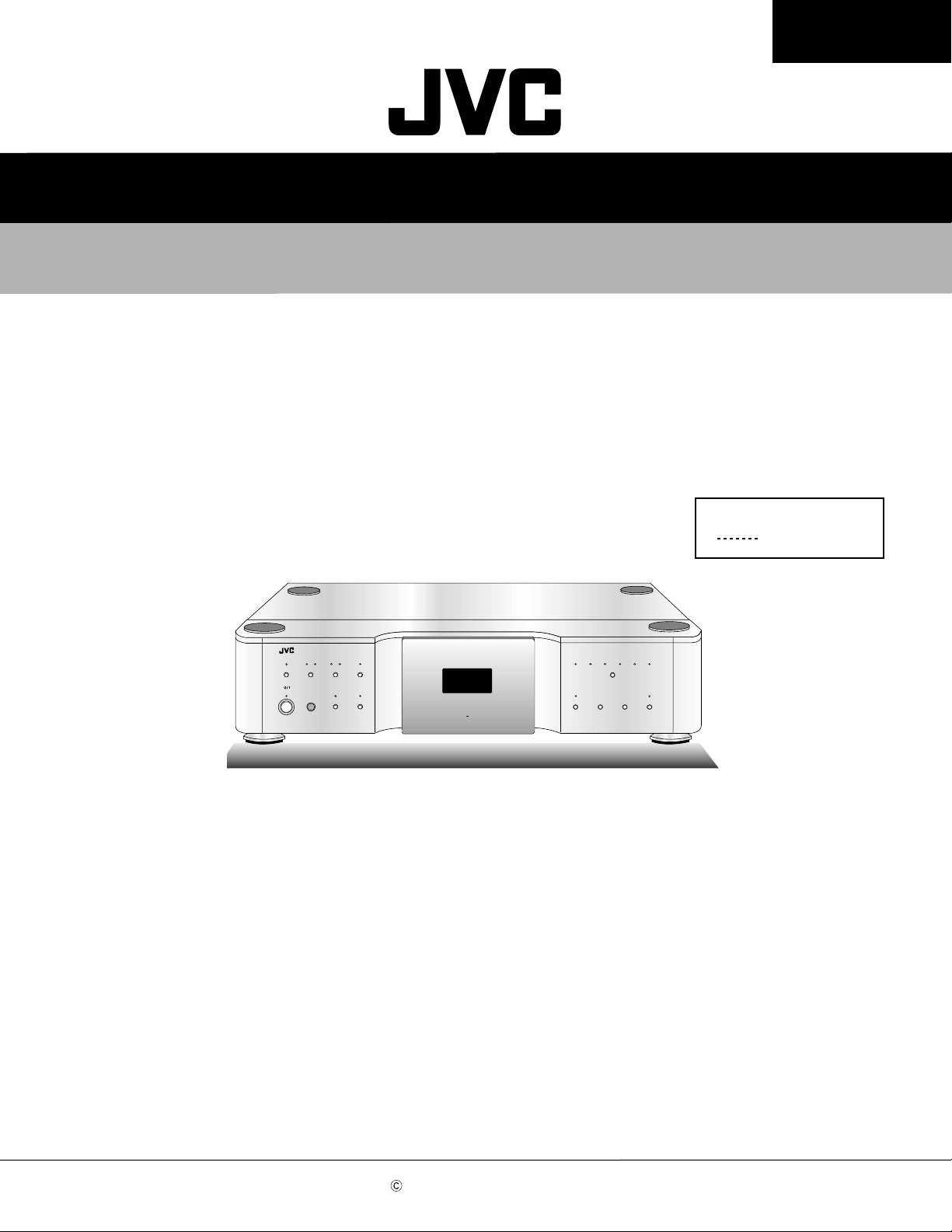
AX-M9000
SERVICE MANUAL
MONAURAL INTEGRATED AMPLIFIER
AX-M9000
Contents
PHASE
SPEAKER
12
-180û 2
STANDBY/ON
PRESENCE
Area Suffix
E Continental Europe
GAIN CONTROL
EXT
PROCESSOR
1
SLEEP
EACH
AX M9000
MONAURAL INTEGRATED AMPLIFIER
LINE
23
45
1
MUTE
DOWN UP
6
ATT
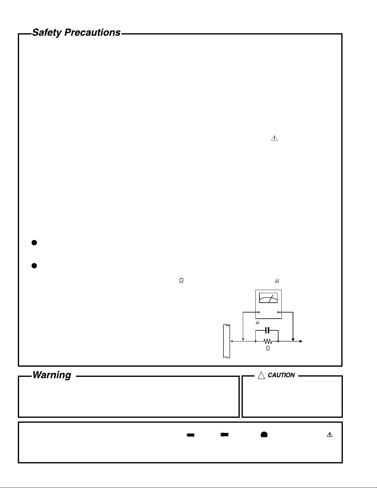
Safety precautions --------------------------------------------------------1-2
Disassembly method -----------------------------------------------------1-3
Adjustment method -------------------------------------------------------1-10
Description of major ICs -------------------------------------------------1-11~21
COPYRIGHT 2001 VICTOR COMPANY OF JAPAN, LTD.
No.20933
Apr.2001
Page 2
AX-M9000
1. This design of this product contains special hardware and many circuits and components specially for safety
purposes. For continued protection, no changes should be made to the original design unless authorized in
writing by the manufacturer. Replacement parts must be identical to those used in the original circuits. Services
should be performed by qualified personnel only.
2. Alterations of the design or circuitry of the product should not be made. Any design alterations of the product
should not be made. Any design alterations or additions will void the manufacturer`s warranty and will further
relieve the manufacture of responsibility for personal injury or property damage resulting therefrom.
3. Many electrical and mechanical parts in the products have special safety-related characteristics. These
characteristics are often not evident from visual inspection nor can the protection afforded by them necessarily
be obtained by using replacement components rated for higher voltage, wattage, etc. Replacement parts which
have these special safety characteristics are identified in the Parts List of Service Manual. Electrical
components having such features are identified by shading on the schematics and by ( ) on the Parts List in
the Service Manual. The use of a substitute replacement which does not have the same safety characteristics
as the recommended replacement parts shown in the Parts List of Service Manual may create shock, fire, or
other hazards.
4. The leads in the products are routed and dressed with ties, clamps, tubings, barriers and the like to be
separated from live parts, high temperature parts, moving parts and/or sharp edges for the prevention of
electric shock and fire hazard. When service is required, the original lead routing and dress should be
observed, and it should be confirmed that they have been returned to normal, after re-assembling.
5. Leakage currnet check (Electrical shock hazard testing)
After re-assembling the product, always perform an isolation check on the exposed metal parts of the product
(antenna terminals, knobs, metal cabinet, screw heads, headphone jack, control shafts, etc.) to be sure the
product is safe to operate without danger of electrical shock.
Do not use a line isolation transformer during this check.
Plug the AC line cord directly into the AC outlet. Using a "Leakage Current Tester", measure the leakage
current from each exposed metal parts of the cabinet, particularly any exposed metal part having a return
path to the chassis, to a known good earth ground. Any leakage current must not exceed 0.5mA AC (r.m.s.).
Alternate check method
Plug the AC line cord directly into the AC outlet. Use an AC voltmeter having, 1,000 ohms per volt or more
sensitivity in the following manner. Connect a 1,500 10W resistor paralleled by a 0.15 F AC-type capacitor
between an exposed metal part and a known good earth ground.
Measure the AC voltage across the resistor with the AC
voltmeter.
Move the resistor connection to eachexposed metal part,
particularly any exposed metal part having a return path to
the chassis, and meausre the AC voltage across the resistor.
Now, reverse the plug in the AC outlet and repeat each
measurement. voltage measured Any must not exceed 0.75 V
AC (r.m.s.). This corresponds to 0.5 mA AC (r.m.s.).
0.15 F AC TYPE
1500 10W
Good earth ground
AC VOLTMETER
(Having 1000
ohms/volts,
or more sensitivity)
Place this
probe on
each exposed
metal part.
!
1. This equipment has been designed and manufactured to meet international safety standards.
2. It is the legal responsibility of the repairer to ensure that these safety standards are maintained.
3. Repairs must be made in accordance with the relevant safety standards.
4. It is essential that safety critical components are replaced by approved parts.
5. If mains voltage selector is provided, check setting for local voltage.
Burrs formed during molding may
be left over on some parts of the
chassis. Therefore, pay attention to
such burrs in the case of
preforming repair of this system.
In regard with component parts appearing on the silk-screen printed side (parts side) of the PWB diagrams, the
parts that are printed over with black such as the resistor ( ), diode ( ) and ICP ( ) or identified by the " "
mark nearby are critical for safety.
When replacing them, be sure to use the parts of the same type and rating as specified by the manufacturer.
(Except the JC version)
1-2
Page 3
AX-M9000
Disassembly method
Removing the metal cover (See Fig. 1)
1.
Remove the three screws A attaching the metal
cover on the back of the body.
2.
Remove the four screws B attaching the metal cover
on both sides of the body using a hexagon wrench.
3.
Draw the metal cover upward from the behind while
pulling the both sides of the lower part of the metal
cover outward.
Removing the front panel assembly
(See Fig. 2 to 5)
Prior to performing the following procedure, remove
the metal cover.
1.
Remove the six screws C attaching the top plate
using a hexagon wrench.
2.
Remove the six screws D and tow screws D'
attaching the front panel assembly from the back of
the body.
Metal cover
B 2
Top plate
A
B 2
Fig.1
C
3.
Remove the four screws E attaching the front panel
assembly from the upper part of the body.
4.
Remove the four screws F attaching the front panel
assembly on both sides of the body.
5.
Disconnect the harness from the connectors CN601,
CN602, CN603, CN604 and CN605 of the system
control board assembly.
6.
Remove the screw G attaching the earth wire.
* The front panel assembly of this machine
comprises the three sets - the front panel
(left), front panel (right) and sub-panel (center).
Front panel assembly
D
D'
Fig.2
F 2
System control board assembly
F 2
Fig.4
Front panel
assembly
G
Earth wire
E
Fig.3
CN602
CN601
CN605
Fig.5
CN603
CN604
1-3
Page 4
AX-M9000
Removing the rear panel (See Fig.6 to 9)
Prior to performing the following procedure, remove
the metal cover and front panel assembly.
1.
Remove the four screws H attaching the rear panel
on the back of the set.
2.
Remove the eight screws I attaching the rear panel
on the upper part of the set.
3.
Remove the six screws J, two screws K, nine screws
L and one screw M attaching the rear panel.
4.
Draw the rear panel upward from the behind at the
legs while pulling the rear panel outward.
5.
Remove the four screws N attaching the speaker
output cord.
* If necessary, remove the power plug, connector
clamp, etc.
Rear panel
(Bottom)
Fig.6
I
Fig.7
M
L
K
H
I
1-4
J
J
L
Rear panel
J
Fig.8
N
Fig.9
N
Page 5
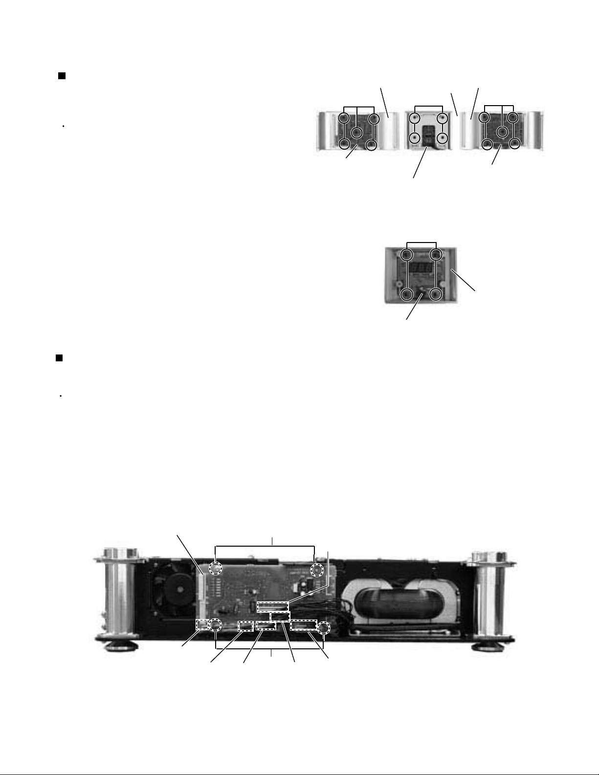
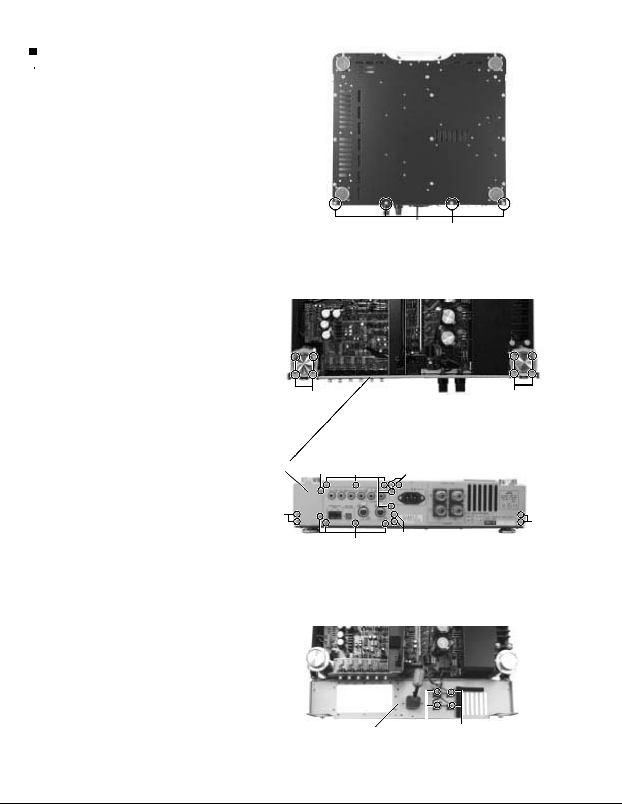
<Removing the front panel section>
AX-M9000
Removing the control switch board
assembly 1 & 2 and display board
assembly (See Fig.10 to 11)
Prior to performing the following procedure, remove
the metal cover and front panel assembly.
Remove the ten screws O attaching the control
1.
switch board assembly 1 & 2 on the back side of the
front panel assembly (left & right sides).
2.
Remove the four screws P attaching the metal base
on the backside of the sub-panel assembly (center).
Remove the four screws Q on the backside of the
3.
metal base. Then the display board assembly can be
removed.
Removing the system control board
assembly (See Fig. 12)
Front panel (right)
O
Control switch board (1)
Metal base
Display board
Sub-panel
P
Fig.10
Q
Fig.11
Front panel (left)
O
Control switch board (2)
Metal base
Prior to performing the following procedure, remove
the metal cover and front panel assembly.
Remove the four screws R attaching the system
1.
control board assembly.
Disconnect the connectors CN611, CN612, CN613,
2.
CN614, CN615 and CN616.
System control board assembly
CN614
CN613 CN616
R
R
CN612
CN611
CN615
Fig.12
1-5
Page 6
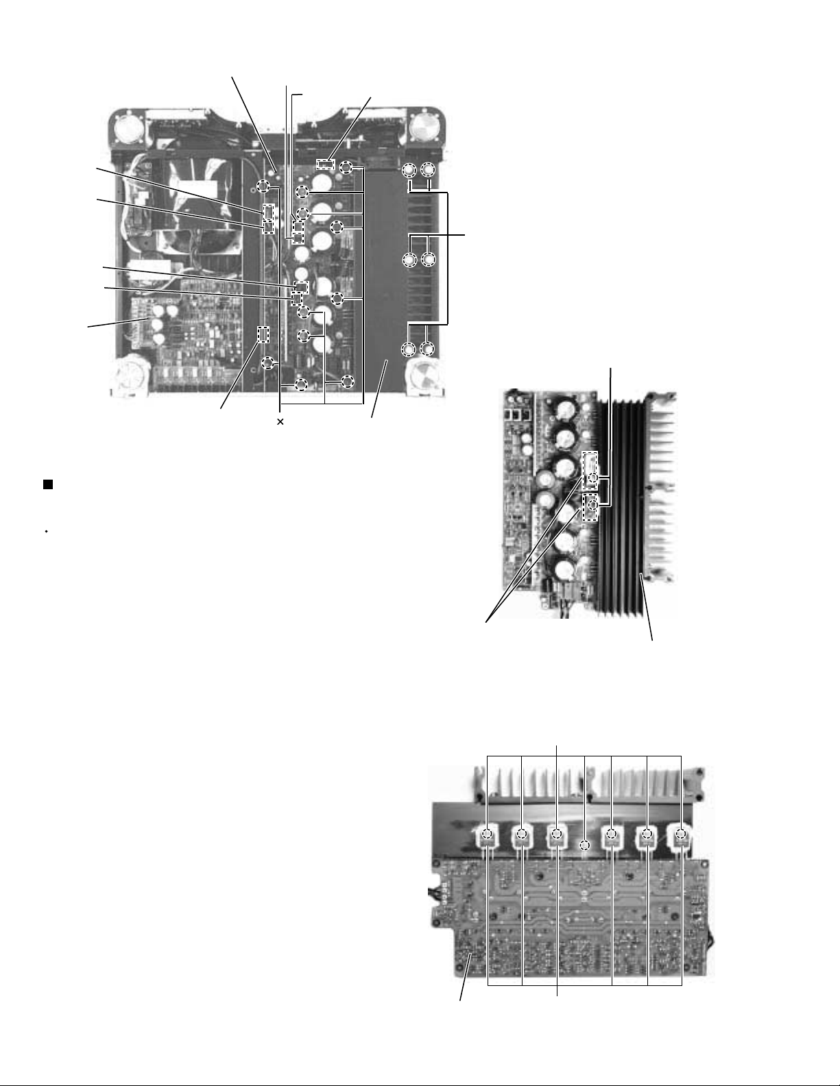
AX-M9000
CN402
CN401
TB403
TB404
Signal
processing
board
Power AMP board
CN301
TB402
T
11
Fig.13
TB401
Heat sink cover
CN453
S
U
Removing the power AMP board
assembly / heat sink (See Fig. 13 to 15)
Prior to performing the following procedure, remove
the metal cover, system control assembly and rear
cover.
Remove the six through bolts S attaching the heat
1.
sink and the heat sink cover.
Remove the eleven screws T attaching the power
2.
AMP sub-board assembly.
Disconnect the harness, which is extending from
3.
power transformer, from the connectors TB401,
TB402, TB403 and TB404.
Disconnect the harness, which is extending from the
4.
power transformer for pre-AMP, from the connectors
CN401 and CN402.
Disconnect the harness, which is extending from the
5.
fan, from the connector CN453.
Disconnect the harness, which is extending from the
6.
signal processing board, from the connector CN301.
Power AMP sub-board
assembly (1) (2)
Heat sink
Fig.14
V
After removing each screw U attaching the power
7.
AMP sub-board assembly (1) & (2), take off the
power AMP sub-board assembly from the heat sink.
Remove the seven screws V attaching transistor
8.
Q335~Q340.
1-6
Power AMP board
Transisitor Q335~Q340.
Fig.15
Page 7
AX-M9000
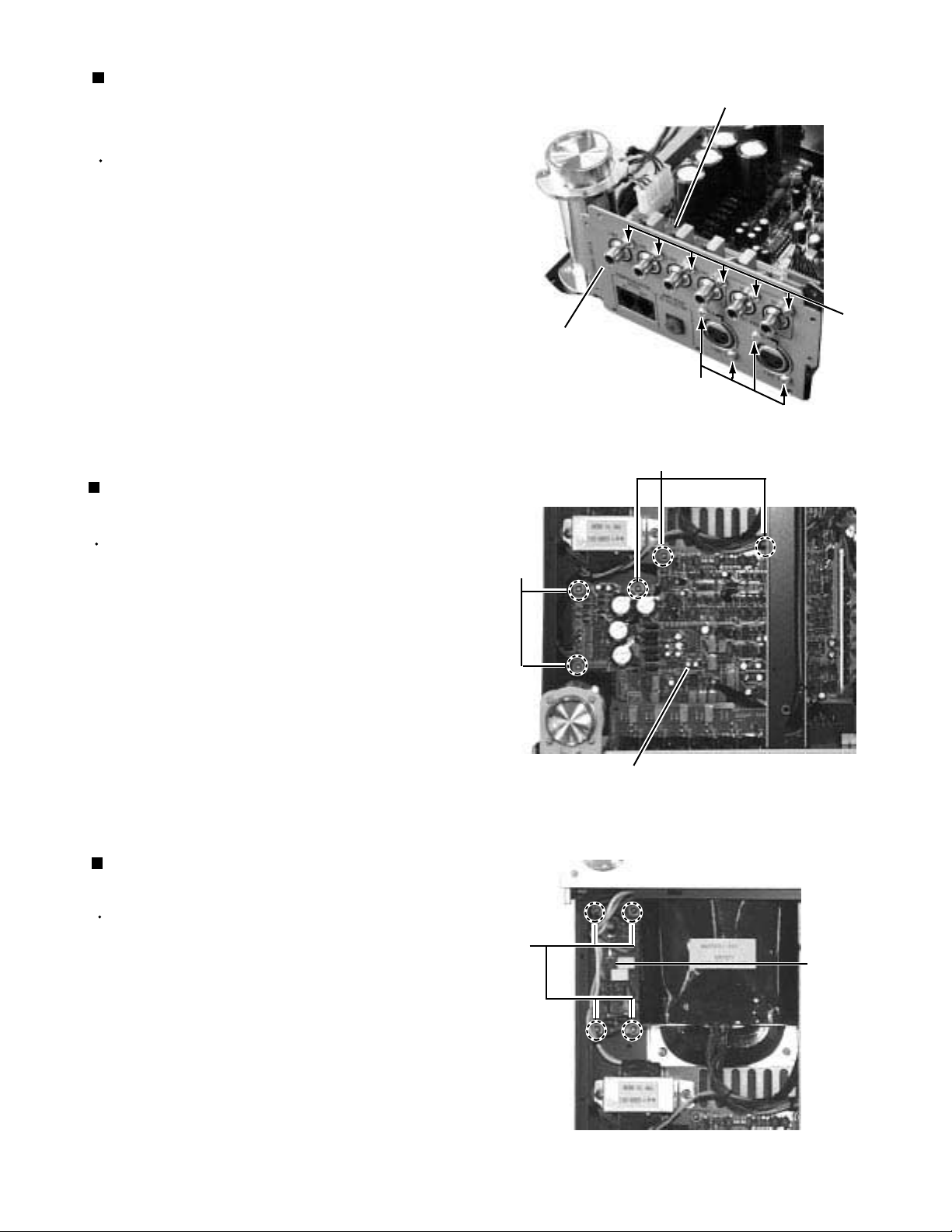
Removing the current mode source
selector board assembly and rear
terminal panel (See Fig. 16)
Prior to performing the following procedure, remove
the metal cover and the rear panel.
1.
Remove the six screws W attaching the RCA pins on
the current mode source selector board assembly.
Then, the current mode source selector board can
be removed.
2.
Remove the four screws X attaching the cannon
connector on the signal processing board.
3.
Then, the rear terminal panel can be removed.
Removing the signal processing board
assembly (See Fig. 17)
Current mode source selector board assembly
W
Rear terminal panel
X
Fig.16
Y
Prior to performing the following procedure, remove
the metal cover and the rear panel.
1.
Remove the current mode source selector board
assembly and the rear terminal panel.
2.
Remove the five screws Y attaching the signal
processing board assembly.
3.
Remove the connectors CN251 and CN252.
Removing the power switch board
assembly (See Fig. 18)
Prior to performing the following procedure, remove
the metal cover.
1.
Remove the four screws Z attaching the power
switch board assembly.
Y
Signal processing board
Fig.17
Z
Power
switch
board
2.
Remove the cable connecting to the transformer.
Fig.18
1-7
Page 8

AX-M9000
Removing the core transformer
for pre-AMP (See Fig. 19)
Prior to performing the following procedure, remove
the metal cover.
1.
Remove the two screws A attaching the power
transformer for pre-AMP.
Removing the transformer
for power AMP (See Fig. 20)
Prior to performing the following procedure, remove
the metal cover and the front panel assembly.
Remove the four screws B attaching the power
1.
transformer for power AMP.
A
Power transformer
for pre-AMP
Fig.19
Power transformer for power AMP
B
1-8
Fig.20
Page 9

AX-M9000
Arrangement drawings for the clamp binding
In order to secure the performance of the machine, refer to the following arrangement drawings
when the lines are clamped.
CLAMP
Orange, Blue wire
Gray wire
Black wire
Purple wire
Red wire
Yellow, Brown wire
CN insertion
CN insertion
Red, Black wire
CN insertion
S CLAMP
White wire
Red wire
S CLAMP
White wire 2
Red wire 2
Fig 1.
CLAMP
CLAMP
WR104WR103
WR102
S CLAMP
Red wire 2
Black wire
CLAMP
S CLAMP
White RED wire
Brown wire
13P
8P
12P
Fig 2.
1-9
Page 10

AX-M9000
Adjustment method
1. List of measuring devices
Measuring devices : Electronic voltmeter
Oscilloscope
Low-frequency transmitter (50Hz-20 kHz of transmitting frequency and output of 0
dBs at the 600 terminal)
Distortion factor tester (with a built-in band path filter)
2. Adjustments and confirmation
Description
Adjusting method
Standard value
Remarks
Standard
output
Total distortion
factor
Output level
Hum noise
Frequency
characteristics
AC voltage of
speaker terminal
Adjustments of
idling currency
1) INPUT LINE1 - Output at the time of THD0.5% at f=1kHz
1) INPUT LINE1 - Distortion factor at the time of
200W (40.0V) at 8 load
1) Output level at the time when inputting 1kHz 200mV
to LINE 1
1) Line 1
2) Base hum
1) Line 1
1) No signal, no load, Vol. 0.0
1) Prior to turning the power on, turn the R398
counterclockwise fully
2) After connecting the 3 pin and 4 pin of the CN303 to the
electronic voltmeter, adjust the voltage to 2-3mV.
3) After elapsing five minutes, adjust the voltage to
3.5+/-0.5mV. Since there is backlash, thoroughly adjust it.
4) After elapsing two minutes, make sure that the voltage
falls within 3.5-7mV. In case where the voltage does not
fall within the specified value, readjust it to the values
specified in 3) above.
Input short
Volume min.
100Hz
1kHz
10kHz
Vol. 99. 5
Vol. 99. 5
Vol. 69. 5
Vol. 44. 0
Vol. 99. 5
More than
210W/8 (41.0V)
20Hz Less than 0.04%
1kHz Less than 0.04%
20kHz Less than 0.06%
192mV +/- 10mV
Less than 10mV
Less than 0.4mV
45.6dB 1dB
45.6dB 1dB
33.4dB 1dB ATT ON
31.0dB 1dB
5.8dB 1dB
45.6dB 1dB
Less than +/- 1mV
Confirmation of
idling currency
Crosstalk
1-10
1) No signal, no load, rated power
Confirm under the room temperature of 20-25
1) INPUT LINE 1 - The output at the
input terminal side shall be +20dBm
as a standard.
The CH to be measured shall be terminated at 10k
Line1
to
Line2
Line1
to
Line5
Five minutes later
after turning the
power on
100Hz More than 70dB
1kHz More than 70dB
10kHz More than 70dB
100Hz More than 70dB
1kHz More than 70dB
10kHz More than 70dB
Page 11

Description of major ICs
BU2114F-X (IC542,543,544) : LED controller
1. Pin layout
AX-M9000
2. Pin function
Pin No.
1
2
3
Symbol
SIN
CK
LATCH
4
5
6
7
8
9
10
11
12
13
14
15
16
17
18
SOUT
EN
RST
GND
GND
GND
08
07
06
05
04
03
02
01
VDD
SIN
CK
LATCH
SOUT
EN
RST
GND
GND
GND
I/O
O
O
O
O
O
O
O
O
O
1
2
3
4
5
6
7
8
9
18
17
16
15
14
13
12
11
10
VDD
01
02
03
04
05
06
07
08
Function
I
I
I
Serial data input terminal
Shift lock of the shift register
When this terminal is set at "L", the latch output will be secured,
In addition, when the output of the shift register is changed during
"H", the latch output will be changed simultaneously.
Output of the shift register at the final stage
I
I
-
-
-
Enable terminals of 01 to 08
Reset of the shift register and latch
Ground
Ground
Ground
Output of the shift register at the 8th stage
Output of the shift register at the 7th stage
Output of the shift register at the 6th stage
Output of the shift register at the 5th stage
Output of the shift register at the 4th stage
Output of the shift register at the 3rd stage
Output of the shift register at the 2nd stage
Output of the shift register at the 1st stage
-
Power supply
1-11
Page 12

AX-M9000
MN101CP10A(IC521) : System controller
1.Pin layout
2. Pin function
Pin No.
Symbol
1
KY10 (DOWN)
2
KY11 (LINE)
3
KY12 (MUTE)
4
TMP IN1
5
TMP IN2
6
VREF+
7
VDD
8
OSC2
9
OSC1
10
VSS
11
XI
12
XO
13
MMOD
14
SADATO
15
SADATI
16
SACLK
17
SBDATO
18
SBDATI
19
SBCLK
20
SREQO
21
RST
22
VOLCS
23
VOLCLK
24
VOLDATO
25
AT T
26
MUTE LED
27
M.WAKE
28
SREQI
29
INH
30
ROT3
31
ROT2
1
~
16
~
4964
48
~
~
33
17
I/O
O
O
O
O
O
O
O
O
O
O
O
32
Pin function
I
Key input 10
I
Key input 11
I
Key input 12
I
Temperature detect 1
I
Temperature detect 2
AD reference voltage
terminal 5.0V
2.0 5.0V supply
Clock out
I
Clock in
0.0V supply
I
GND
Open
I
Memory extended mode
SA data out
I
SA data in
SA clock
SB data out
I
SB data in
I
SB clock
Request for the communication
output between the sets
I
Reset terminal
VOL. CS
VOL. clock
VOL. out
Input ATT
Mute LED
I
Return form the stop mode
I
Request for the communication
output between the sets
I
INM
I
Rotary input 3
I
Rotary input 2
Pin No.
32
33
34
35
36
37
38
39
40
41
42
43
44
45
46
47
48
49
50
51
52
53
54
55
56
57
58
59
60
61
62
63
64
Symbol
ROT1
C
B
A
POWER
ABS
MONPRO
ALLEACH
PRESEN1
PRESEN2
SPKB
SPKA
FANH
GM1
GM2
HPS
LRST
FANL
LDATO
LCLK
LACH
B.CON
RM
KY1 (HPS)
KY2 (EACH)
KY3 (PRO)
KY4 (PRE)
KY5 (SP)
KY6 (PHASE)
VSS
KY7 (POWER)
KY8 (ATT)
KY9 (UP)
I/O
Pin function
I
Rotary input 1
O
Line decoder C
O
Line decoder B
O
Line decoder A
O
Power SW
O
Absolute phase SW
O
MON/ PRO SW
O
All each (LED)
O
Presence SW1
O
Presence SW2
O
Speaker B
O
Speaker A
O
Fan control High
O
GM volume output 1
O
GM volume output 2
O
HPS filter SW
O
Serial/ Parallel IC reset
O
Fan control LOW
O
Serial/ Parallel IC out data
O
Serial/ Parallel IC clock
O
Latch
O
Brightness control
O
Remote control input
I
Key input 1
I
Key input 2
I
Key input 3
I
Key input 4
I
Key input 5
I
Key input 6
(GND)
I
Key input 7
I
Key input 8
I
Key input 9
1-12
Page 13

NJM2903M-XE(IC454) : Temperature detector
1. Pin layout
A OUTPUT
1
8
V
AX-M9000
+
A -INPUT
A +INPUT
GND
2. Block diagram
+
V
D101
2
3
4
Q110
(TOP VIEW)
Q109
D103
Q111
D104
D102
7
6
5
Q112
B OUTPUT
B -INPUT
B +INPUT
Q8
Q7
Q1
+INPUT
-INPUT
GND
Q101
Q103
Q105
Q104
Q106
Q102
Q107
Q108
Q5
Q6
OUTPUT
Q4
Q3
R1
Q2
1-13
Page 14

AX-M9000
NJM5532M-D-W(IC152,153) : Presence circuit amp
1. Pin layout
2. Block diagram
+INPUT
INPUT
A OUT
A - IN
A + IN
V -
1
2
3
4
8
7
6
5
V +
B OUT
B - IN
B + IN
V+
OUTPUT
V
1-14
Page 15

OPA134PA(IC108, 201, 301) : OP Amp.
Pin layout
Offset Trim
1
8
AX-M9000
Offset Trim
2
- In
+ In
V -
3
4
-
+
8-Pin DIP, SO-8
TC74HC04AF(IC264) : Data line buffer
Pin layout
14
13
12
11
10
Vcc
6A
6Y
5A
5Y
4A
9
1A
1Y
2A
2Y
3A
3Y
1
2
3
4
5
6
V +
7
6
Output
5
NC
A
L
H
Y
H
L
GND
4Y
7
(TOP VIEW)
8
1-15
Page 16

AX-M9000
TC74HC238AF-X(IC525) : Line recorder
1. Pin layout
2. Truth table
ENABLE
G1 G2A
L
X
X
H
H
H
H
H
H
H
H
A
B
C
G2A
G2B
G1
Y7
GND
INPUTS
SELECT
CB
G2B
X
X
X
XXXX
H
X
H
X
LL
L
L
L
LL
LL
L
LL
LL
H
LL
LL
H
HH
LL
1
2
3
4
5
6
7
8
(TOP VIEW)
A
X
X
XX
L
H
L
H
H
H
LLLL
L
H
L
H
HH
16
Vcc
15
Y0
14
Y1
13
Y2
12
Y3
11
Y4
10
Y5
Y6
9
OUTPUTS
Y0 Y1 Y2
Y3
Y4
Y5
Y6 Y7
LLLLLLLL
LLLLLLLL
LLL
H
LLLLLLL
L
L
L
L
H
H
L
L
L
LLLL
LLLLL
LLLLLL
L
L
L
L
L
L
L
H
H
L
L
L
L
L
L
L
L
L
L
H
L
H
LLLLLLL
X : Don't Care
SELECTED OUTPUT
NONE
NONE
L
NONE
L
L
L
L
L
L
H
Y0
Y1
Y2
Y3
Y4
Y5
Y6
Y7
3. Block diagram
SELECT
INOUT
1-16
A
B
C
ENABLE
INPUTS
15
Y0
14
Y1
1
2
3
4
G2A
5
G2B
6
G1
13
Y2
12
Y3
DATA
Y4
Y5
Y6
Y7
OUTPUTS
11
10
9
7
Page 17

TC74HC27AF-W(IC531) : Noa gate
1. Pin layout
AX-M9000
2. Truth table
1A
1B
2A
2B
2C
2Y
GND
1
2
3
4
5
6
7
(TOP VIEW)
14
13
12
11
10
Vcc
1C
1Y
3C
3B
3A
9
3Y
8
TC74VHC08F-X(IC281) : Dataline buffer
1. Terminal layout
14
1A
1
Vcc
AB
XL
H
X
H
X
X
L
L
X : Don't Care
2. Truth table
A
L
B
C
Y
X
L
X
L
H
L
H
Y
L
L
1B
1Y
2A
2B
2Y
GND
13
12
11
10
9
8
4B
4A
4Y
3B
3A
3Y
2
3
4
5
6
7
(TOP VIEW)
L
H
H
H
L
HH
X : Don't Care
L
L
1-17
Page 18

AX-M9000
TC74HC373HF-X(IC522, IC523, IC524) : Shift register for relay control
1. Pin layout
1
OE
Q0
2
3
D0
4
D1
5
Q1
6
Q2
D2
7
D3
8
9
Q3
GND
10
(TOP VIEW)
20
19
18
17
16
15
14
13
12
11
Vcc
Q7
D7
D6
Q6
Q5
D5
D4
Q4
LE
2. Truth table
INPUTS
OE
H
L
L
L
X : Don't Care
Z : High impedance
Qn: The Q output level immediately
before the LE becomes to "L".
LE
X
L
H
H
D
X
X
L
H
OUTPUTS
Q
Z
Qn
L
H
3. Block diagram
LE
OE
D0
34
D1
D
L
D
Q
L
Q0
D2 D3 D4
7
Q
52
Q1
813
D
L
D
Q
L
6
Q2
D5
14
D
Q
9
Q3
Q
L
12
Q4 Q5
D6
17
D
Q
L
15
D7
18
D
L
D
Q
16
Q6
Q
L
19
Q7
1-18
Page 19

TC74VHC123AF-X(IC532) : Monostable multivibrator
1. Pin layout
16
15
14
13
12
11
10
9
Vcc
1Rx/Cx
1Cx
1Q
2Q
2CLR
2B
2A
1A
1B
1CLR
1Q
2Q
1Cx
2Rx/Cx
GND
1
2
3
4
5
6
7
8
(TOP VIEW)
AX-M9000
2. Block diagram
X/CX
R
C
X
A
B
CLR
3. Timing diagram
A
B
CLR
RX/CX
Q
Q
t
w OUT
V
CC
Vref Vref
L
-
Q
Q
N
+
P
V
CC
R
D
Q
F/F
CK
Q
t
w OUT
C2
+
-
t
rr
H
t
w OUT+
Q
Q
V
IH
V
IL
V
IH
V
IL
V
IH
V
IL
V
CC
VrefH
VrefL
GND
V
OH
V
OL
V
OH
V
OL
t
rr
1-19
Page 20

AX-M9000
UPC1237HA (IC453) : Protection IC
1. Pin layout
12
2. Block diagram
R4
D1
R5
2
Q1
R3
1
Q2
34
R6
Q4
D4
D2
D3
5678
3
R9
Q6
R10
Q5
R11
Q20
R13
Q8
R14
Q7
8
D7
Q15
D6
Q16
R22
R24
R25
75
R16
R15
Q9
R17
R19
Q10
Q11
R18
R20
Q12
R21
Q13
Q14
4
R26
6
Q17
Q18
R27
Q19
R28
1-20
Page 21

VC5022-2(IC302) : Advanced super A
Block diagram
AX-M9000
1
2
3
4
R1
1.6k
Q1
9
Q10
8
R7
1.6k
Q9
7
Q2
R3
1.6k
R8
220
6
Q3
Q4
Q5
Q6
R4
R2
220
51
Q7
R5
51
Q8
R6
51
5
1-21
Page 22

AX-M9000
VICTOR COMPANY OF JAPAN, LIMITED
AUDIO & COMMUNICATION BUSINESS DIVISION
PERSONAL & MOBILE NETWORK BUSINESS UNIT. 10-1,1chome,Ohwatari-machi,Maebashi-city,371-8543,Japan
(No.20933)
Printed in Japan
200104(V)
 Loading...