

Page 1
AX-M9000
SERVICE MANUAL
MONAURAL INTEGRATED AMPLIFIER
AX-M9000
Contents
PHASE
SPEAKER
12
-180û 2
STANDBY/ON
PRESENCE
Area Suffix
E Continental Europe
GAIN CONTROL
EXT
PROCESSOR
1
SLEEP
EACH
AX M9000
MONAURAL INTEGRATED AMPLIFIER
LINE
23
45
1
MUTE
DOWN UP
6
ATT
Safety precautions --------------------------------------------------------1-2
Disassembly method -----------------------------------------------------1-3
Adjustment method -------------------------------------------------------1-10
Description of major ICs -------------------------------------------------1-11~21
COPYRIGHT 2001 VICTOR COMPANY OF JAPAN, LTD.
No.20933
Apr.2001
Page 2
AX-M9000
1. This design of this product contains special hardware and many circuits and components specially for safety
purposes. For continued protection, no changes should be made to the original design unless authorized in
writing by the manufacturer. Replacement parts must be identical to those used in the original circuits. Services
should be performed by qualified personnel only.
2. Alterations of the design or circuitry of the product should not be made. Any design alterations of the product
should not be made. Any design alterations or additions will void the manufacturer`s warranty and will further
relieve the manufacture of responsibility for personal injury or property damage resulting therefrom.
3. Many electrical and mechanical parts in the products have special safety-related characteristics. These
characteristics are often not evident from visual inspection nor can the protection afforded by them necessarily
be obtained by using replacement components rated for higher voltage, wattage, etc. Replacement parts which
have these special safety characteristics are identified in the Parts List of Service Manual. Electrical
components having such features are identified by shading on the schematics and by ( ) on the Parts List in
the Service Manual. The use of a substitute replacement which does not have the same safety characteristics
as the recommended replacement parts shown in the Parts List of Service Manual may create shock, fire, or
other hazards.
4. The leads in the products are routed and dressed with ties, clamps, tubings, barriers and the like to be
separated from live parts, high temperature parts, moving parts and/or sharp edges for the prevention of
electric shock and fire hazard. When service is required, the original lead routing and dress should be
observed, and it should be confirmed that they have been returned to normal, after re-assembling.
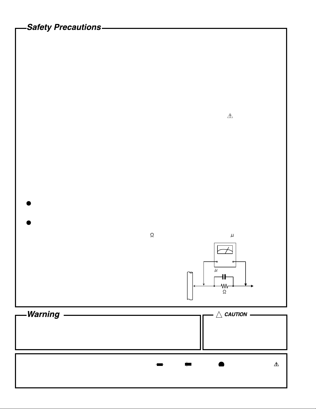
5. Leakage currnet check (Electrical shock hazard testing)
After re-assembling the product, always perform an isolation check on the exposed metal parts of the product
(antenna terminals, knobs, metal cabinet, screw heads, headphone jack, control shafts, etc.) to be sure the
product is safe to operate without danger of electrical shock.
Do not use a line isolation transformer during this check.
Plug the AC line cord directly into the AC outlet. Using a "Leakage Current Tester", measure the leakage
current from each exposed metal parts of the cabinet, particularly any exposed metal part having a return
path to the chassis, to a known good earth ground. Any leakage current must not exceed 0.5mA AC (r.m.s.).
Alternate check method
Plug the AC line cord directly into the AC outlet. Use an AC voltmeter having, 1,000 ohms per volt or more
sensitivity in the following manner. Connect a 1,500 10W resistor paralleled by a 0.15 F AC-type capacitor
between an exposed metal part and a known good earth ground.
Measure the AC voltage across the resistor with the AC
voltmeter.
Move the resistor connection to eachexposed metal part,
particularly any exposed metal part having a return path to
the chassis, and meausre the AC voltage across the resistor.
Now, reverse the plug in the AC outlet and repeat each
measurement. voltage measured Any must not exceed 0.75 V
AC (r.m.s.). This corresponds to 0.5 mA AC (r.m.s.).
0.15 F AC TYPE
1500 10W
Good earth ground
AC VOLTMETER
(Having 1000
ohms/volts,
or more sensitivity)
Place this
probe on
each exposed
metal part.
!
1. This equipment has been designed and manufactured to meet international safety standards.
2. It is the legal responsibility of the repairer to ensure that these safety standards are maintained.
3. Repairs must be made in accordance with the relevant safety standards.
4. It is essential that safety critical components are replaced by approved parts.
5. If mains voltage selector is provided, check setting for local voltage.
Burrs formed during molding may
be left over on some parts of the
chassis. Therefore, pay attention to
such burrs in the case of
preforming repair of this system.
In regard with component parts appearing on the silk-screen printed side (parts side) of the PWB diagrams, the
parts that are printed over with black such as the resistor ( ), diode ( ) and ICP ( ) or identified by the " "
mark nearby are critical for safety.
When replacing them, be sure to use the parts of the same type and rating as specified by the manufacturer.
(Except the JC version)
1-2
Page 3
AX-M9000
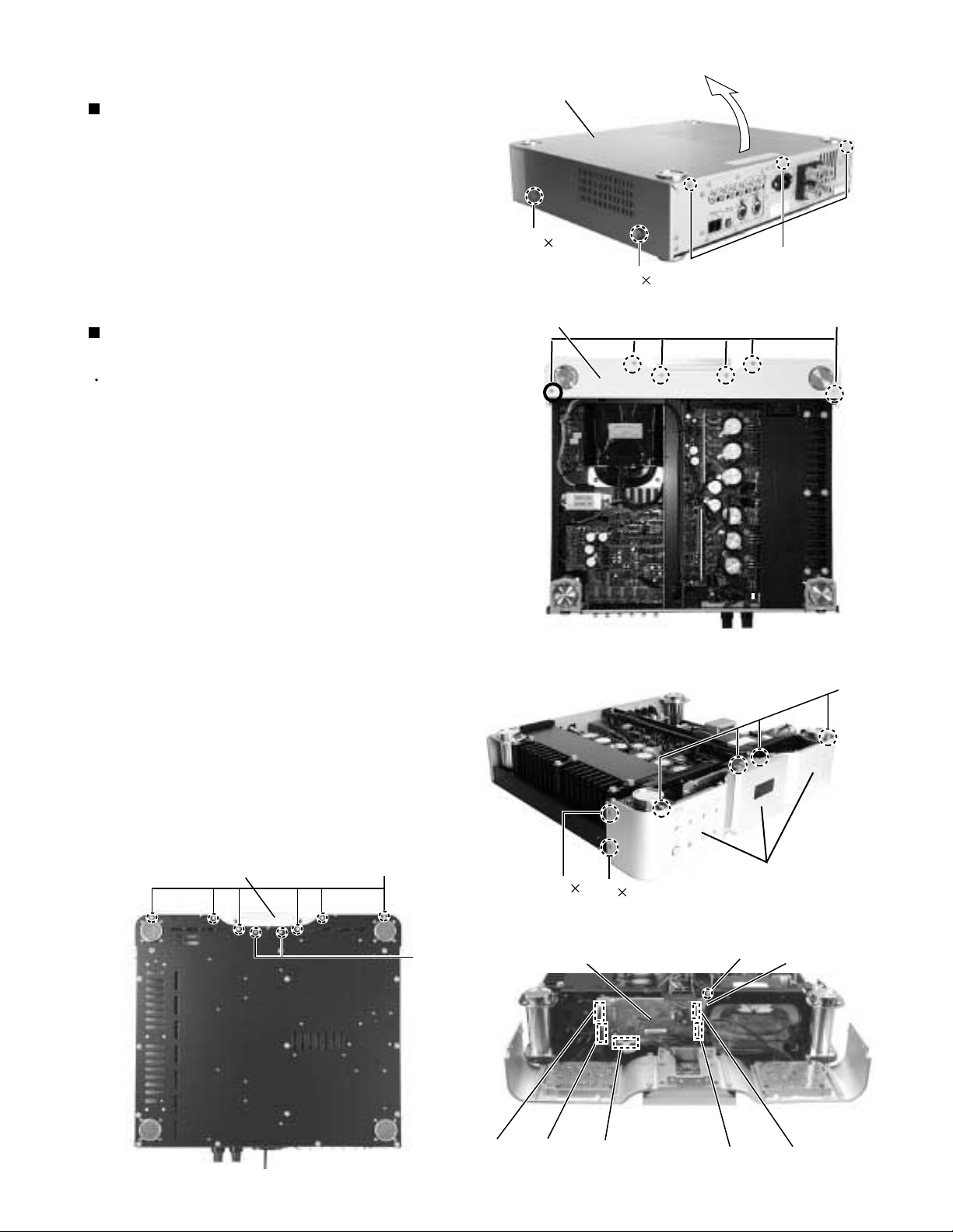
Disassembly method
Removing the metal cover (See Fig. 1)
1.
Remove the three screws A attaching the metal
cover on the back of the body.
2.
Remove the four screws B attaching the metal cover
on both sides of the body using a hexagon wrench.
3.
Draw the metal cover upward from the behind while
pulling the both sides of the lower part of the metal
cover outward.
Removing the front panel assembly
(See Fig. 2 to 5)
Prior to performing the following procedure, remove
the metal cover.
1.
Remove the six screws C attaching the top plate
using a hexagon wrench.
2.
Remove the six screws D and tow screws D'
attaching the front panel assembly from the back of
the body.
Metal cover
B 2
Top plate
A
B 2
Fig.1
C
3.
Remove the four screws E attaching the front panel
assembly from the upper part of the body.
4.
Remove the four screws F attaching the front panel
assembly on both sides of the body.
5.
Disconnect the harness from the connectors CN601,
CN602, CN603, CN604 and CN605 of the system
control board assembly.
6.
Remove the screw G attaching the earth wire.
* The front panel assembly of this machine
comprises the three sets - the front panel
(left), front panel (right) and sub-panel (center).
Front panel assembly
D
D'
Fig.2
F 2
System control board assembly
F 2
Fig.4
Front panel
assembly
G
Earth wire
E
Fig.3
CN602
CN601
CN605
Fig.5
CN603
CN604
1-3
Page 4
AX-M9000
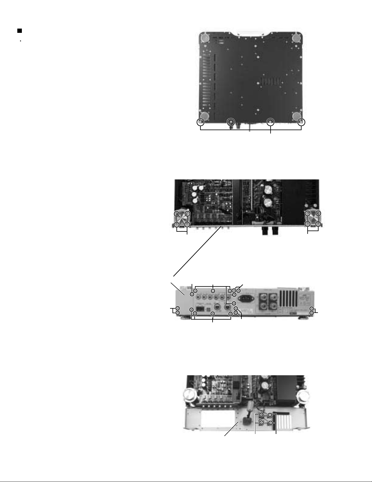
Removing the rear panel (See Fig.6 to 9)
Prior to performing the following procedure, remove
the metal cover and front panel assembly.
1.
Remove the four screws H attaching the rear panel
on the back of the set.
2.
Remove the eight screws I attaching the rear panel
on the upper part of the set.
3.
Remove the six screws J, two screws K, nine screws
L and one screw M attaching the rear panel.
4.
Draw the rear panel upward from the behind at the
legs while pulling the rear panel outward.
5.
Remove the four screws N attaching the speaker
output cord.
* If necessary, remove the power plug, connector
clamp, etc.
Rear panel
(Bottom)
Fig.6
I
Fig.7
M
L
K
H
I
1-4
J
J
L
Rear panel
J
Fig.8
N
Fig.9
N
Page 5
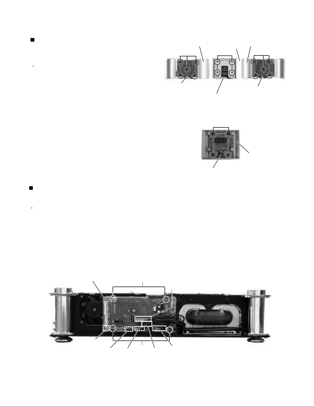
<Removing the front panel section>
AX-M9000
Removing the control switch board
assembly 1 & 2 and display board
assembly (See Fig.10 to 11)
Prior to performing the following procedure, remove
the metal cover and front panel assembly.
Remove the ten screws O attaching the control
1.
switch board assembly 1 & 2 on the back side of the
front panel assembly (left & right sides).
2.
Remove the four screws P attaching the metal base
on the backside of the sub-panel assembly (center).
Remove the four screws Q on the backside of the
3.
metal base. Then the display board assembly can be
removed.
Removing the system control board
assembly (See Fig. 12)
Front panel (right)
O
Control switch board (1)
Metal base
Display board
Sub-panel
P
Fig.10
Q
Fig.11
Front panel (left)
O
Control switch board (2)
Metal base
Prior to performing the following procedure, remove
the metal cover and front panel assembly.
Remove the four screws R attaching the system
1.
control board assembly.
Disconnect the connectors CN611, CN612, CN613,
2.
CN614, CN615 and CN616.
System control board assembly
CN614
CN613 CN616
R
R
CN612
CN611
CN615
Fig.12
1-5
Page 6
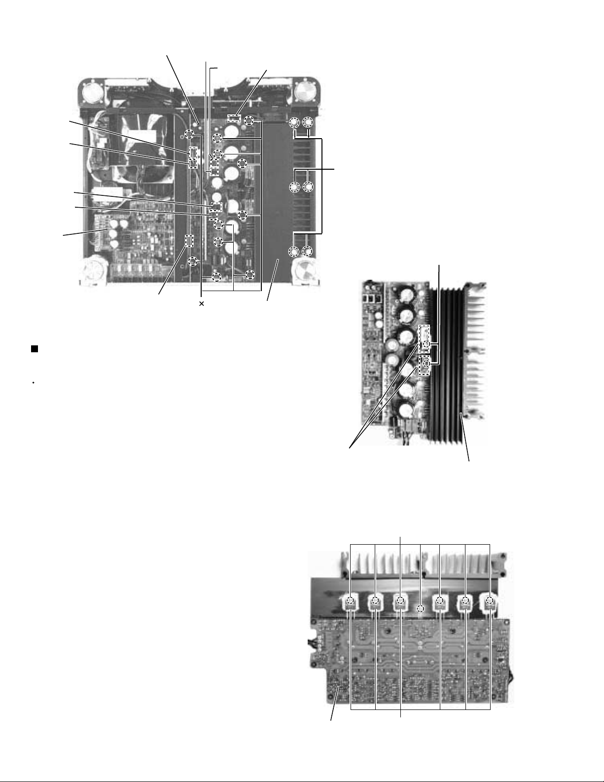
AX-M9000
CN402
CN401
TB403
TB404
Signal
processing
board
Power AMP board
CN301
TB402
T
11
Fig.13
TB401
Heat sink cover
CN453
S
U
Removing the power AMP board
assembly / heat sink (See Fig. 13 to 15)
Prior to performing the following procedure, remove
the metal cover, system control assembly and rear
cover.
Remove the six through bolts S attaching the heat
1.
sink and the heat sink cover.
Remove the eleven screws T attaching the power
2.
AMP sub-board assembly.
Disconnect the harness, which is extending from
3.
power transformer, from the connectors TB401,
TB402, TB403 and TB404.
Disconnect the harness, which is extending from the
4.
power transformer for pre-AMP, from the connectors
CN401 and CN402.
Disconnect the harness, which is extending from the
5.
fan, from the connector CN453.
Disconnect the harness, which is extending from the
6.
signal processing board, from the connector CN301.
Power AMP sub-board
assembly (1) (2)
Heat sink
Fig.14
V
After removing each screw U attaching the power
7.
AMP sub-board assembly (1) & (2), take off the
power AMP sub-board assembly from the heat sink.
Remove the seven screws V attaching transistor
8.
Q335~Q340.
1-6
Power AMP board
Transisitor Q335~Q340.
Fig.15
Page 7
AX-M9000
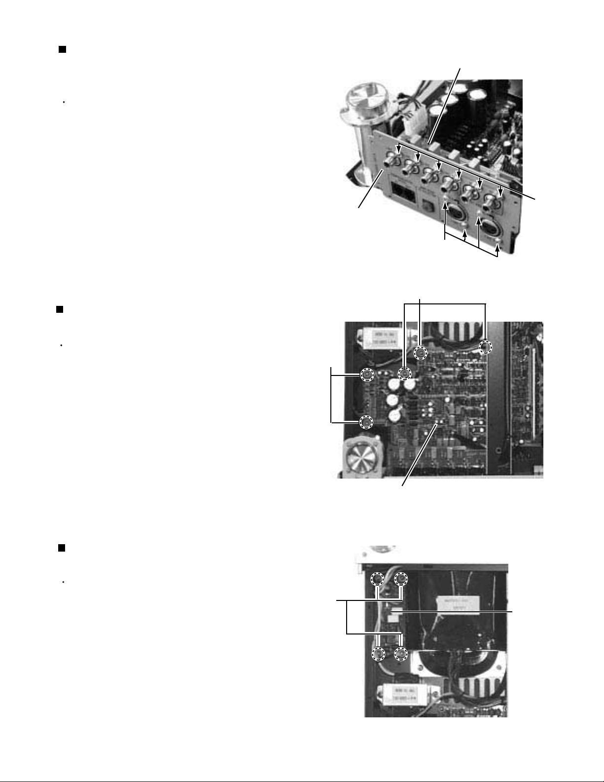
Removing the current mode source
selector board assembly and rear
terminal panel (See Fig. 16)
Prior to performing the following procedure, remove
the metal cover and the rear panel.
1.
Remove the six screws W attaching the RCA pins on
the current mode source selector board assembly.
Then, the current mode source selector board can
be removed.
2.
Remove the four screws X attaching the cannon
connector on the signal processing board.
3.
Then, the rear terminal panel can be removed.
Removing the signal processing board
assembly (See Fig. 17)
Current mode source selector board assembly
W
Rear terminal panel
X
Fig.16
Y
Prior to performing the following procedure, remove
the metal cover and the rear panel.
1.
Remove the current mode source selector board
assembly and the rear terminal panel.
2.
Remove the five screws Y attaching the signal
processing board assembly.
3.
Remove the connectors CN251 and CN252.
Removing the power switch board
assembly (See Fig. 18)
Prior to performing the following procedure, remove
the metal cover.
1.
Remove the four screws Z attaching the power
switch board assembly.
Y
Signal processing board
Fig.17
Z
Power
switch
board
2.
Remove the cable connecting to the transformer.
Fig.18
1-7
Page 8
AX-M9000
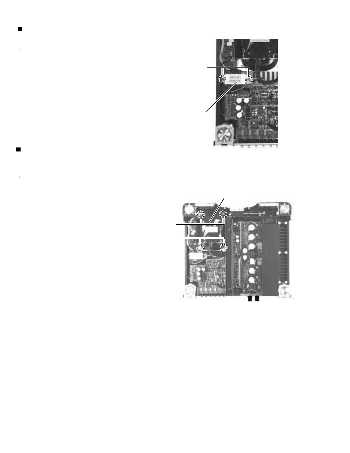
Removing the core transformer
for pre-AMP (See Fig. 19)
Prior to performing the following procedure, remove
the metal cover.
1.
Remove the two screws A attaching the power
transformer for pre-AMP.
Removing the transformer
for power AMP (See Fig. 20)
Prior to performing the following procedure, remove
the metal cover and the front panel assembly.
Remove the four screws B attaching the power
1.
transformer for power AMP.
A
Power transformer
for pre-AMP
Fig.19
Power transformer for power AMP
B
1-8
Fig.20
Page 9
AX-M9000
Arrangement drawings for the clamp binding
In order to secure the performance of the machine, refer to the following arrangement drawings
when the lines are clamped.
CLAMP
Orange, Blue wire
Gray wire
Black wire
Purple wire
Red wire
Yellow, Brown wire
CN insertion
CN insertion
Red, Black wire
CN insertion
S CLAMP
White wire
Red wire
S CLAMP
White wire 2
Red wire 2
Fig 1.
CLAMP
CLAMP
WR104WR103
WR102
S CLAMP
Red wire 2
Black wire
CLAMP
S CLAMP
White RED wire
Brown wire
13P
8P
12P
Fig 2.
1-9
Page 10
AX-M9000
Adjustment method
1. List of measuring devices
Measuring devices : Electronic voltmeter
Oscilloscope
Low-frequency transmitter (50Hz-20 kHz of transmitting frequency and output of 0
dBs at the 600 terminal)
Distortion factor tester (with a built-in band path filter)
2. Adjustments and confirmation
Description
Adjusting method
Standard value
Remarks
Standard
output
Total distortion
factor
Output level
Hum noise
Frequency
characteristics
AC voltage of
speaker terminal
Adjustments of
idling currency
1) INPUT LINE1 - Output at the time of THD0.5% at f=1kHz
1) INPUT LINE1 - Distortion factor at the time of
200W (40.0V) at 8 load
1) Output level at the time when inputting 1kHz 200mV
to LINE 1
1) Line 1
2) Base hum
1) Line 1
1) No signal, no load, Vol. 0.0
1) Prior to turning the power on, turn the R398
counterclockwise fully
2) After connecting the 3 pin and 4 pin of the CN303 to the
electronic voltmeter, adjust the voltage to 2-3mV.
3) After elapsing five minutes, adjust the voltage to
3.5+/-0.5mV. Since there is backlash, thoroughly adjust it.
4) After elapsing two minutes, make sure that the voltage
falls within 3.5-7mV. In case where the voltage does not
fall within the specified value, readjust it to the values
specified in 3) above.
Input short
Volume min.
100Hz
1kHz
10kHz
Vol. 99. 5
Vol. 99. 5
Vol. 69. 5
Vol. 44. 0
Vol. 99. 5
More than
210W/8 (41.0V)
20Hz Less than 0.04%
1kHz Less than 0.04%
20kHz Less than 0.06%
192mV +/- 10mV
Less than 10mV
Less than 0.4mV
45.6dB 1dB
45.6dB 1dB
33.4dB 1dB ATT ON
31.0dB 1dB
5.8dB 1dB
45.6dB 1dB
Less than +/- 1mV
Confirmation of
idling currency
Crosstalk
1-10
1) No signal, no load, rated power
Confirm under the room temperature of 20-25
1) INPUT LINE 1 - The output at the
input terminal side shall be +20dBm
as a standard.
The CH to be measured shall be terminated at 10k
Line1
to
Line2
Line1
to
Line5
Five minutes later
after turning the
power on
100Hz More than 70dB
1kHz More than 70dB
10kHz More than 70dB
100Hz More than 70dB
1kHz More than 70dB
10kHz More than 70dB
Page 11

Description of major ICs
BU2114F-X (IC542,543,544) : LED controller
1. Pin layout
AX-M9000
2. Pin function
Pin No.
1
2
3
Symbol
SIN
CK
LATCH
4
5
6
7
8
9
10
11
12
13
14
15
16
17
18
SOUT
EN
RST
GND
GND
GND
08
07
06
05
04
03
02
01
VDD
SIN
CK
LATCH
SOUT
EN
RST
GND
GND
GND
I/O
O
O
O
O
O
O
O
O
O
1
2
3
4
5
6
7
8
9
18
17
16
15
14
13
12
11
10
VDD
01
02
03
04
05
06
07
08
Function
I
I
I
Serial data input terminal
Shift lock of the shift register
When this terminal is set at "L", the latch output will be secured,
In addition, when the output of the shift register is changed during
"H", the latch output will be changed simultaneously.
Output of the shift register at the final stage
I
I
-
-
-
Enable terminals of 01 to 08
Reset of the shift register and latch
Ground
Ground
Ground
Output of the shift register at the 8th stage
Output of the shift register at the 7th stage
Output of the shift register at the 6th stage
Output of the shift register at the 5th stage
Output of the shift register at the 4th stage
Output of the shift register at the 3rd stage
Output of the shift register at the 2nd stage
Output of the shift register at the 1st stage
-
Power supply
1-11
Page 12

AX-M9000
MN101CP10A(IC521) : System controller
1.Pin layout
2. Pin function
Pin No.
Symbol
1
KY10 (DOWN)
2
KY11 (LINE)
3
KY12 (MUTE)
4
TMP IN1
5
TMP IN2
6
VREF+
7
VDD
8
OSC2
9
OSC1
10
VSS
11
XI
12
XO
13
MMOD
14
SADATO
15
SADATI
16
SACLK
17
SBDATO
18
SBDATI
19
SBCLK
20
SREQO
21
RST
22
VOLCS
23
VOLCLK
24
VOLDATO
25
AT T
26
MUTE LED
27
M.WAKE
28
SREQI
29
INH
30
ROT3
31
ROT2
1
~
16
~
4964
48
~
~
33
17
I/O
O
O
O
O
O
O
O
O
O
O
O
32
Pin function
I
Key input 10
I
Key input 11
I
Key input 12
I
Temperature detect 1
I
Temperature detect 2
AD reference voltage
terminal 5.0V
2.0 5.0V supply
Clock out
I
Clock in
0.0V supply
I
GND
Open
I
Memory extended mode
SA data out
I
SA data in
SA clock
SB data out
I
SB data in
I
SB clock
Request for the communication
output between the sets
I
Reset terminal
VOL. CS
VOL. clock
VOL. out
Input ATT
Mute LED
I
Return form the stop mode
I
Request for the communication
output between the sets
I
INM
I
Rotary input 3
I
Rotary input 2
Pin No.
32
33
34
35
36
37
38
39
40
41
42
43
44
45
46
47
48
49
50
51
52
53
54
55
56
57
58
59
60
61
62
63
64
Symbol
ROT1
C
B
A
POWER
ABS
MONPRO
ALLEACH
PRESEN1
PRESEN2
SPKB
SPKA
FANH
GM1
GM2
HPS
LRST
FANL
LDATO
LCLK
LACH
B.CON
RM
KY1 (HPS)
KY2 (EACH)
KY3 (PRO)
KY4 (PRE)
KY5 (SP)
KY6 (PHASE)
VSS
KY7 (POWER)
KY8 (ATT)
KY9 (UP)
I/O
Pin function
I
Rotary input 1
O
Line decoder C
O
Line decoder B
O
Line decoder A
O
Power SW
O
Absolute phase SW
O
MON/ PRO SW
O
All each (LED)
O
Presence SW1
O
Presence SW2
O
Speaker B
O
Speaker A
O
Fan control High
O
GM volume output 1
O
GM volume output 2
O
HPS filter SW
O
Serial/ Parallel IC reset
O
Fan control LOW
O
Serial/ Parallel IC out data
O
Serial/ Parallel IC clock
O
Latch
O
Brightness control
O
Remote control input
I
Key input 1
I
Key input 2
I
Key input 3
I
Key input 4
I
Key input 5
I
Key input 6
(GND)
I
Key input 7
I
Key input 8
I
Key input 9
1-12
Page 13

NJM2903M-XE(IC454) : Temperature detector
1. Pin layout
A OUTPUT
1
8
V
AX-M9000
+
A -INPUT
A +INPUT
GND
2. Block diagram
+
V
D101
2
3
4
Q110
(TOP VIEW)
Q109
D103
Q111
D104
D102
7
6
5
Q112
B OUTPUT
B -INPUT
B +INPUT
Q8
Q7
Q1
+INPUT
-INPUT
GND
Q101
Q103
Q105
Q104
Q106
Q102
Q107
Q108
Q5
Q6
OUTPUT
Q4
Q3
R1
Q2
1-13
Page 14

AX-M9000
NJM5532M-D-W(IC152,153) : Presence circuit amp
1. Pin layout
2. Block diagram
+INPUT
INPUT
A OUT
A - IN
A + IN
V -
1
2
3
4
8
7
6
5
V +
B OUT
B - IN
B + IN
V+
OUTPUT
V
1-14
Page 15

OPA134PA(IC108, 201, 301) : OP Amp.
Pin layout
Offset Trim
1
8
AX-M9000
Offset Trim
2
- In
+ In
V -
3
4
-
+
8-Pin DIP, SO-8
TC74HC04AF(IC264) : Data line buffer
Pin layout
14
13
12
11
10
Vcc
6A
6Y
5A
5Y
4A
9
1A
1Y
2A
2Y
3A
3Y
1
2
3
4
5
6
V +
7
6
Output
5
NC
A
L
H
Y
H
L
GND
4Y
7
(TOP VIEW)
8
1-15
Page 16

AX-M9000
TC74HC238AF-X(IC525) : Line recorder
1. Pin layout
2. Truth table
ENABLE
G1 G2A
L
X
X
H
H
H
H
H
H
H
H
A
B
C
G2A
G2B
G1
Y7
GND
INPUTS
SELECT
CB
G2B
X
X
X
XXXX
H
X
H
X
LL
L
L
L
LL
LL
L
LL
LL
H
LL
LL
H
HH
LL
1
2
3
4
5
6
7
8
(TOP VIEW)
A
X
X
XX
L
H
L
H
H
H
LLLL
L
H
L
H
HH
16
Vcc
15
Y0
14
Y1
13
Y2
12
Y3
11
Y4
10
Y5
Y6
9
OUTPUTS
Y0 Y1 Y2
Y3
Y4
Y5
Y6 Y7
LLLLLLLL
LLLLLLLL
LLL
H
LLLLLLL
L
L
L
L
H
H
L
L
L
LLLL
LLLLL
LLLLLL
L
L
L
L
L
L
L
H
H
L
L
L
L
L
L
L
L
L
L
H
L
H
LLLLLLL
X : Don't Care
SELECTED OUTPUT
NONE
NONE
L
NONE
L
L
L
L
L
L
H
Y0
Y1
Y2
Y3
Y4
Y5
Y6
Y7
3. Block diagram
SELECT
INOUT
1-16
A
B
C
ENABLE
INPUTS
15
Y0
14
Y1
1
2
3
4
G2A
5
G2B
6
G1
13
Y2
12
Y3
DATA
Y4
Y5
Y6
Y7
OUTPUTS
11
10
9
7
Page 17

TC74HC27AF-W(IC531) : Noa gate
1. Pin layout
AX-M9000
2. Truth table
1A
1B
2A
2B
2C
2Y
GND
1
2
3
4
5
6
7
(TOP VIEW)
14
13
12
11
10
Vcc
1C
1Y
3C
3B
3A
9
3Y
8
TC74VHC08F-X(IC281) : Dataline buffer
1. Terminal layout
14
1A
1
Vcc
AB
XL
H
X
H
X
X
L
L
X : Don't Care
2. Truth table
A
L
B
C
Y
X
L
X
L
H
L
H
Y
L
L
1B
1Y
2A
2B
2Y
GND
13
12
11
10
9
8
4B
4A
4Y
3B
3A
3Y
2
3
4
5
6
7
(TOP VIEW)
L
H
H
H
L
HH
X : Don't Care
L
L
1-17
Page 18

AX-M9000
TC74HC373HF-X(IC522, IC523, IC524) : Shift register for relay control
1. Pin layout
1
OE
Q0
2
3
D0
4
D1
5
Q1
6
Q2
D2
7
D3
8
9
Q3
GND
10
(TOP VIEW)
20
19
18
17
16
15
14
13
12
11
Vcc
Q7
D7
D6
Q6
Q5
D5
D4
Q4
LE
2. Truth table
INPUTS
OE
H
L
L
L
X : Don't Care
Z : High impedance
Qn: The Q output level immediately
before the LE becomes to "L".
LE
X
L
H
H
D
X
X
L
H
OUTPUTS
Q
Z
Qn
L
H
3. Block diagram
LE
OE
D0
34
D1
D
L
D
Q
L
Q0
D2 D3 D4
7
Q
52
Q1
813
D
L
D
Q
L
6
Q2
D5
14
D
Q
9
Q3
Q
L
12
Q4 Q5
D6
17
D
Q
L
15
D7
18
D
L
D
Q
16
Q6
Q
L
19
Q7
1-18
Page 19

TC74VHC123AF-X(IC532) : Monostable multivibrator
1. Pin layout
16
15
14
13
12
11
10
9
Vcc
1Rx/Cx
1Cx
1Q
2Q
2CLR
2B
2A
1A
1B
1CLR
1Q
2Q
1Cx
2Rx/Cx
GND
1
2
3
4
5
6
7
8
(TOP VIEW)
AX-M9000
2. Block diagram
X/CX
R
C
X
A
B
CLR
3. Timing diagram
A
B
CLR
RX/CX
Q
Q
t
w OUT
V
CC
Vref Vref
L
-
Q
Q
N
+
P
V
CC
R
D
Q
F/F
CK
Q
t
w OUT
C2
+
-
t
rr
H
t
w OUT+
Q
Q
V
IH
V
IL
V
IH
V
IL
V
IH
V
IL
V
CC
VrefH
VrefL
GND
V
OH
V
OL
V
OH
V
OL
t
rr
1-19
Page 20

AX-M9000
UPC1237HA (IC453) : Protection IC
1. Pin layout
12
2. Block diagram
R4
D1
R5
2
Q1
R3
1
Q2
34
R6
Q4
D4
D2
D3
5678
3
R9
Q6
R10
Q5
R11
Q20
R13
Q8
R14
Q7
8
D7
Q15
D6
Q16
R22
R24
R25
75
R16
R15
Q9
R17
R19
Q10
Q11
R18
R20
Q12
R21
Q13
Q14
4
R26
6
Q17
Q18
R27
Q19
R28
1-20
Page 21

VC5022-2(IC302) : Advanced super A
Block diagram
AX-M9000
1
2
3
4
R1
1.6k
Q1
9
Q10
8
R7
1.6k
Q9
7
Q2
R3
1.6k
R8
220
6
Q3
Q4
Q5
Q6
R4
R2
220
51
Q7
R5
51
Q8
R6
51
5
1-21
Page 22

AX-M9000
VICTOR COMPANY OF JAPAN, LIMITED
AUDIO & COMMUNICATION BUSINESS DIVISION
PERSONAL & MOBILE NETWORK BUSINESS UNIT. 10-1,1chome,Ohwatari-machi,Maebashi-city,371-8543,Japan
(No.20933)
Printed in Japan
200104(V)
Page 23

PARTS LIST
[ AX-M9000 ]
* All printed circuit boards and its assemblies are not available as service parts.
AX-M9000
Area suffix
E ----------- Continental Europe
- Contents -
Exploded view of general assembly and parts list
Electrical parts list
Packing materials and accessories parts list
3- 3
3- 6
3-14
3-1
Page 24

AX-M9000
< MEMO >
3-2
Page 25

Block diagram
AX-M9000
DC Servo
RY
SPK 2
for
Rectifire(3)
Output Stage
AVR
Main AC Lines
AC
Primary
Rectifire
for
AVR
for
ID
Select
Section
for
Drive Stage
Pre driv
RY
Fan
Reset
Inhibit
Inrush
ON/OFF
AVR
AVR
AVR
AVR
for
AD Gm
Volume
for
OpAmp
Function
for
Digital
Vol Cont
for
I/V
Convert
Thermal
Thermal
5
Super A
Advanced
GmR
SPKRYSPK
SPK 1
4
(-ch)
Input Gm
Curent Invert (+ch)
Presence
3
Advanced Gm Volume
Imp A
GmR
Imp B
Presence
Curent Invert (-ch)
(+ch)
Input Gm
Relay
Driver
Disply
Volume
Luch
RM
Reciv
Compa.
Thermal
c o m
V/I
(-ch)
Con
Vol Cont.
V/I
Con
V/I
Con
Indicator
MJ
Send
Convert
Bal Unbal
Processor
(+ch)
Vol Cont.
V/I
V/I
Con
Con
V/I
Con
V/I
Con
2
1
MJ
Cont.
Sleep
Reciv
V/I
Con
Key Input
LINE 1
A
LINE 2
LINE 3
LINE 4
LINE 5
LINE 6
BC D
Output
EXT
Input
2-1
Page 26

AX-M9000
< MEMO >
2-2
Page 27

Standard schematic diagrams
System control section
Q526
5
1.5
C501
IC511
GP1U561
C511
120
R501
D501
1.5
C502
SLR-342MC-T
C512
0.01
100/6.3
130
R502
C513
D502
1.5
C503
SLR-342DC-T
S511
R511
1.5
QSW0802-001Z
10K
4
120
130
R521
D521
1.5
C522
SLR-342MC-T
R522
D522
1.5
C523
SLR-342DC-T
S521
QSW0802-001Z
1.5
C521
3
C535
C536
R531
10k
1.5
2
330
R541
1.5
C531
IC542 IC543 IC544
BU2114F-X BU2114F-X BU2114F-X
R548
R547
R546
R545
R544
R543
R542
330
330
330
330
330
330
330
1
120
R503
D503
C514
130
R523
D523
1.5
C532
1.5
C504
SLR-342MC-T
S512
QSW0802-001Z
R512
10K
1.5
1.5
C524
SLR-342DC-T
S522
QSW0802-001Z
R532
10k
1.5
330
R504
D504
C515
130
R524
D524
C537
330
330
R550
R549
DTA114YKA-X
1.5
C505
SLR-342VC-T
S513
R513
1.5
1.5
C525
SLR-342DC-T
S523
R533
1.5
IC541
LB-403VD
330
330
R552
R551
120
R505
D505
QSW0802-001Z
C516
10K
130
R525
D525
QSW0802-001Z
C538
10k
330
330
330
R555
R554
R553
1.5
C506
SLR-342MC-T
S514
R514
10K
1.5
1.5
C526
SLR-342DC-T
S524
R534
10k
1.5
330
R556
120
R506
SLR-342MC-T
D506
QSW0802-001Z
C517
1.5
130
R526
SLR-342DC-T
D526
QSW0802-001Z
C539
1.5
1.5
C533
1.5
C507
S515
R515
1.5
C527
S525
R535
R518
QSW0802-001Z
10K
10k
120
R507
D507
SLR-342MC-T
S516
C518
R516
1.5
130
R527
1.5
C528
SLR-342DC-T
D527
QSW0802-001Z
D558 D559
1SS133-T2 1SS133-T2
Q527
330
330
330
330
R560
R559
R558
R557
C596C594
330P330P
1.5
C508
R519
QSW0802-001Z
C519
10K
CN502
330
R528
D528
DTB113ZK-X
330
330
330
R563
R562
R561
K505
K506
K507
K508
C597C595
330P330P
120
R508
D508
SLR-342MC-T
S517
R517
10K
1.5
CN511
SLR-342VC-T
D560
1SS133-T2
R586
10K
DTC114YKA-X
Q528
330
R564
C534
100/6.3
AX-M9000
CN501
QGA2001C1-10
CN601
ALL_L
PRO_L
ABS_L
PWR_L
PRE1_L
PRE2_L
SPB
SPA
HPS_L
D543
1SS133-T2
1SS133-T2
ATT_L
L6_L
L5_L
L1_L
L2_L
L3_L
L4_L
MUTE_L
IC531
IC531
IC531
IC531
TC74HC27AF-W
R594
NI
R571
1k
C592
1.5
IC532
TC74VHC123AF-X
C593
1.5
IC532
TC74VHC123AF-X
R593
10K
D553
1SS133-T2
C576
1/50
TC74VHC123AF-X
D557
1SS133-T2
C581
1/50
IC532
TC74VHC123AF-X
LS
HS
Q504
DTD123TK-X
Q594
DTB143EK-X
Q505
DTD123TK-X
HPS_L
Q506
DTD123TK-X
PRE1_L
Q507
DTD123TK-X
PRE2_L
Q508
DTD123TK-X
PWR_L
ABS_L
Q511
DTD123TK-X
PRO_L
Q512
DTD123TK-X
ALL_L
MUTE_L
L4_L
Q513
DTD123TK-X
L3_L
Q514
DTD123TK-X
L2_L
Q515
DTD123TK-X
L1_L
Q516
DTD123TK-X
L5_L
Q517
DTD123TK-X
L6_L
Q518
DTD123TK-X
ATT_L
Q519
DTD123TK-X
IC526
TC7S08F
IC527
TC7S08F
IC528
TC7S08F
C541
1.5
IC522
TC74HC373AF-X
22K
22K
22K
R583
R584
ROT1
ROT2
ROT3
D552
11E2-T5
C578
2.2/50
SADATO
SADATI
SREQI
SREQO
SBCLK
SBDATI
SBDATO
SACLK
R582D556
100k
IC521
MN101CP10A
R572
1M
C571
1.5
C572
470/6.3
C573
R575
10K
IC532
R576
10K
470/6.3
R579
10k
DTC114YKA-X DTC114YKA-X
C604
390P
X501
QAX0246-001Z
D551
1SS119-02-T2
R573
220
C574
47000/6.3
C575
470/6.3
R580
1k
Q524 Q525
1SS133-T2
R585
C542
1.5
DAT
SCK
CS
C544
1.5
IC525
TC74HC238AF-X
R581
10k
C580C579
0.010.01
K501
SADATO
100P100P
SADATI
SACLK
K502
SBDATO
SBDATI
SBCLK
K503
C600C601
100P
K504
SREQO
SREQI
100P
ROT3
ROT2
ROT1
C603 C602
QGA2001C1-13
CN611
C543
1.5
10k
QGA2001C1-07
CN612
C599
330P
IC523
TC74HC373AF-X
IC524
TC74HC373AF-X
D591R591
NI
Q591
DTC114YKA-X
C591
100/10
GM2
GM1
HS
DTB143EK-X
QGA2001C1-08 QGA2001C1-03
CN613 CN614
LS
SPA
SPB
Q593
Q592
DTC114YKA-X
GM1
GM2
HPS
PRE1
PRE2
SPB
SPA
ABS
PRO
L4
L3
L2
L1
L5
L6
ATT
to WR102
PRE1
sheet 2/2
PRE2
CN616
QGA2001C1-08
L1
L2
L3
L4
L5
L6
PRO
to WR103
ATT
HPS
sheet 2/2
ABS
CN615
QGA2001C1-12
to WR104 to WR451 to WR452
sheet 2/2 sheet 2/2 sheet 2/2
SHEET 1/2
120
R595
NI
R509
1.5
C509
SLR-342MC-T
D509
CN602
QGA2001C1-12
D531
D532
D533
D534
D535
D536
1SS133-T2
1SS133-T2
1SS133-T2
1SS133-T2
1SS133-T2
CN603
QGA2001C1-10
D537
D538
D539
D540
D541
1SS133-T2
1SS133-T2
1SS133-T2
1SS133-T2
CN512
CN513
CN604
QGA2001C1-08
CN605
QGA2001C1-07
1SS133-T2
IC531
TC74HC27AF-W
TC74HC27AF-W
TC74HC27AF-W
TC74HC27AF-W
R574
C598
0.47
10k
AB CD E F G
2-3
Page 28

AX-M9000
Main section (Premain AMP., Power supply)
C110
33P
R129
15k
R132 C109
470 22/25
IC108
OPA134PA
R131
100k
R130
15k
Q286
R280
DTA114YKA-X
3.3k
Q273
2SC2878/AB/-T
5
WR112
WJA0013-001A
CN111
QGA2001C1-13
R133
470
C108
100P
J108
QNN0085-001
4
3
2
J107
QNN0085-001
J103
QNN0085-001
J104
QNN0085-001
J105
QNN0085-001
J106
QNN0085-001
R107
15k
C107
R117
RY103
R113
15k
R103
C113
C123
1.5
RY104
R104
15k
R114
C104
C124
1.5
RY105
R105
15k
R115
C105
C125
1.5
RY106
R106
15k
R116
C106
C126
1.5
QNZ0204-001
J102 J101
QNZ0204-001
1.5
C151
C153
10/25
1
IC153
NJM5532M-D-W
10/25
C154
RY107
C127
1.5
R111
15k
C111
R101
15k
C101
R112
15k
C112
R102
15k
C102
RY151
IC152
NJM5532M-D-W
R154 R156
NJM5532M-D-W
C157
C155
47/25
47/25
R151
220
R153
R157
220
220k
C158
C156
47/25
47/25
R152
150
R158
220k
150 150
1.5
C152
IC152
R155
220
RY101
C121
1.5
RY102
C122
1.5
RY152
IC153
NJM5532M-D-W
Q287
DTC114YKA-X
L1
5.6V
L2
10/2510/25
C159C160
D286
1SS133-T2
R291
R292
100k
10
C291
22/25
IC151
CS3310-KP
C246
100P
C247
100P
C248
100P
PRE1
PRE2
TC74HC04AF-W
R274
2.2k
K271
R275
2.2k
K272
R276
2.2k
K273
IC264
2SC2545/E/
1ss133
D201
D202
D203
1ss133
1ss13322k 22k
D204R203 R201
Q202
2SA1084/E/
C261
10/25
IC253
NJM7805FA
C263
10/25
C264
10/25
IC254
NJM7905FA
C262
10/25
IC252
NJM7905FA
C259
100/25
C260
100/25
IC264
TC74HC04AF-W
IC264
TC74HC04AF-W
IC264
TC74HC04AF-W
IC264
TC74HC04AF-W
IC264
TC74HC04AF-W
Q201
1ss133
C205
RY108
C128
1.5
R209R211
0.1
A
820820
8282
R205R207
NJM7805FA
IC255
NJM7815FA
IC256
NJM7915FA
390
R271
IC251
390
R272
PRO
C201
C202
1200P
2SA1084/E/-T
Q203
R300
1200P
390
R273
2SA1084/E/-T2SC2545/E/-T
Q205Q206
390
2SC2545/E/-T
Q204
CP251
ICP-N10
C265
0.01
C266
0.01
CP252
ICP-N10
1.5
C271
R127
12k
R125
RY141
3.9k
2.2
RY600
RY500
R400
120k
C400
12P
R319
120K
C319
1
C303
10P
C421
0.01
C422
0.01
CN401
QGA3903C1-03
WR1
WJA0017-001A
R381
R383
A
22k
R389R391Q383
82022
Q381
A
2SB649A/C/
220 220
R387 R385
2SC2546
R302
220
A
IC301
OPA134PA
Q384
2SA1084/E/-T
220
R388
22820
R392R390
A
R382 Q382
A
K1
K2
K3
220
R386
R384
A
22k
2.2 2SD669A/C/
Q456
DTA114YKA-X
Q455
DTA114YKA-X
A
D401
F10KF20
F10KF20
P3+
A
A
D403
F10KF20
F10KF20 F10KF20
C401 C403 C405 C407
2700/100 2700/100 2700/100 1000/100
C402 C404 C406 C408
2700/100 2700/100 2700/100 1000/100
AA
D402
F10KF20
F10KF20
A
AA
D404
P3-
F10KF20
A
D417
R401
11E2-T2
18k
A
D418
11E2-T2
D419
11E2-T2
C1
1.0
A
RY1
C2
AA
0.01
A
A
F1
R143
3.9k
C129
1.5
R145
12k
C143
C141
10/25
33P
R147
22k
1ss133
22k
100
IC141
LM6172IN
R128
12k
R126
3.9k
R144
3.9k
R146
12k
C144
33P
R148
100
IC141
LM6172IN
Q225
2SA1084/E/-T
2SC2545/E/-T
Q221
3900P3900P
C221C222
Q227
2SA1084/E/-T
Q223
2SC2545/E/-T
D205D206
1ss1331ss133
C223
3900P
C224
3900P
Q224
2SA1084/E/-T
D208
1ss133
Q228
2SC2545/E/-T
Q226
2SC2545/E/-T
Q222
2SA1084/E/-T
1k
R250
Q251
R255
820
R259
22
R257
220
R261
220
C253
0.022
C254
0.022
R262
220
R258
220
R260
22
R256
820
DTC114YKA
Q256
Q252
2SD669A/C/
IC261IC262IC263
PC817CDPC817CDPC817CD
100P
100P
100P
100P
C285
C284
C290
C287
C288
R141
100k
RY142
C130
1.5
C142
10/25
R142
100k
ATT
R202
Q207
2SC2545/E/
C206 R206R208 R210
0.1 8282 820
D207
Q208
2SA1084/E/
820
R204
R212
C204 C203
1200P 1200P
2SB649A/C/
Q253
2SC2545/E/-T
C255
4.7/50
C257
1000/50
C258
C256
1000/50
4.7/50
Q254
2SA1084/E/-T
J271
QNZ0444-001
C145
10/25
C150
1k820
R249R221
820
R223
820820
R224R222
Q255
DTA114YKA
R253
D259
A
D260
A
2.7k
R254
Q261
DTC114YKA-X
100P
C283
R150 R149
C146
10/25
R225
33
R231
33
R232
33
R226
33
R228
2.7k
HZ30-1L-T2
HZ30-1L-T2
33k
R266
ICP-N10
5.6V
R270
100P
C286
15k
R227
15k
CP257
ICP-N10
R265
R267
CP258
330
100P
22k
L102
9.1k 9.1k 3.3k
R234 R233 R229
3.3k
R230
11DF2-FA11
11DF2-FA11
11DF2-FA11
11DF2-FA11
Q257
DTA114YKA
10K
Q259
2SA1037AK/RS/
11DF2-FA11
A
A
QSW0870-001
QSW0870-001
QSW0870-001
QSW0870-001
100P
C289
R285
1k
R286
1k
R287
1k
R289
1k
R288
1k
R290
1k
R294
1k
R293
1k
L101
C225
R237R240
R239
R238
C226
A
A
A
D257
C251
1000/50
1000/50
C252
A
D258
A
11DF2-FA11
11DF2-FA11
11DF2-FA11
K284
K285
K286
K287
K289
K288
K290
K291
K292
C131
22/25
1k18k
18k
1k
22/25
RY143
D251
D253
D255
D256
D252
D254
S271
S271
S271
S271
HPS
2SC2545/E/-T
Q229
Q230
2SA1084/E/-T
C132
1.5
ABS
R244
1k
D282
1SS133-T2
47k
R282
DTC114YKA
Q258
C297
100P
C296
100P
C295
100P
IC281
TC74VHC08F-X
IC281
TC74VHC08F-X
IC281
TC74VHC08F-X
IC281
TC74VHC08F-X
IC281
TC74VHC08F-X
IC281
TC74VHC08F-X
RY144
C281
10/50
R277
R278
R279
C241
1
IC201
OPA134PA
D281
MTZJ5.1C-T2
C282
330
330
330
GND
GND
R295
1k
R296
1k
R297
1k
4.7/50
C300
GND
MUTE
SCLK
DATA
CS
PRE1
PRE2
5.6V
GND
L1
L2
L3
L4
L5
L6
PRO
ATT
HPS
ABS
R281
10k
R283
1.5
R241
33
R245
33
10k
QGA3903C1-03
QGA3903C1-03
K281
K282
K283
Q281
2SC2240/GL/-T
K251
K252
K253
K254
K255
K256
K257
K258
K259
K260
K261
K262
K263
K264
K265
K266
K267
K268
CN251
CN252
WR102 WR101
WR103
WR104
WJA0016-001A
C600
150P
R600
4.7k
C306
270P
C599
0.1
C500
33P
R500
27k
C304
47P
C499
0.1
R301
100
QGA2503C1-04
CN301
330k
R320
C305
100P 1SS133
TB401
QNZ0446-001
TB402
QNZ0446-001
TB403
QNZ0446-001
TB404
QNZ0446-001
to CN616
sheet 1/2
WJA0014-001A WJK0077-001A
WJA0015-001A
to CN615
sheet 1/2
to CN611
sheet 1/2
A
D301
HZ3ALL-T2
A
D381
HZ16-3L-T2
D303
HZ3ALL-T2
C381
0.022
C383
100/50
R393
2.2k
Q301
R379
2SC4001
2.2K
3.9k3.9k
150P150P
R303R304
C301C302
R380
2.2K
Q302
2SA1546
R394
2.2k
C384
100/50
C382
0.022
HZ3ALL-T2
D382
HZ16-3L-T2
F10KF20
A
D405
F10KF20 F10KF20
P2+
A
D407 D411
D406
D410
F10KF20
D408
D412
P2-
F10KF20
CP403
A
ICP-N50 ICP-N10
C409
22/50
C3
1.0
A
RY2
C4
0.01
R2R1
A
3.3( 5W) 3.3( 5W)
HZ3ALL-T2
A
D409 D413
P1+
P1-
CP401
A
C410
1000/50
TB32
TB31
AUDIO SIGNAL
R309
D304
A
D302
A
A
F10KF20
AA
F10KF20
A
F10KF20
15K
D415
D414
D416
D307D308
1SS133-T21SS133-T2
TB22
TB21
TB11
TB12
R305
A
220
R307
100
D309
1SS82
R395
680
Q313
2SC2240/GL/-T
R398
470
2SA970/GL/-T
Q314
D310
1SS82
R308
100
A
R306
220
P0+
P0-
IC401
NJM78M24FA
C411
0.1
Q303Q307Q308Q304
2SA1084/E/-T
A
2SA1546/K/2SC4001/K/
R399
ERT-Q2WFL351S
R396
180
C395
0.0047
R397
150
2SC2545/E/-T
A
C412
47/35
R311
2.2k
C311
33P
2SC2240/GL/-T
Q395
2SD1200F/QR/
2SA970/GL/-T
C312
33P
R312
2.2k
D471
D473
A
2SA1546/K/
Q309
A
IC302
VC5022-2
Q310
2SC4001/K/
1SS133
1SS133
Q451
2SA965/OY/-T
A
R313
680
Q311
Q312
R314
680
Q471
1SS133
D472
2SC2878
0.001
C451
D451
1SS133-T2
Q452
DTC114YKA-X
D420
11E2-T2
D421
11E2-T2
R402
11E2-T2 MTZJ5.1C-T2
R315
A
470
R317
47k
C313
C314
A
R316
R471
27k
220k
R451
D452
1SS133-T2
27k
R453
3.9k
A
D422 D423
R325R327
0.1
R328R326
0.1
R318
470
Q453
A
ICP-N20
D311
HZ3ALL-T2
R321
A
120
1.8k620
Q325
2SC458/D/-T
A
A
6201.8k
A
Q326
2SA1029/D/-T
A
47k
D312
HZ3ALL-T2
R472
8.2k
R452
10k
R454
DTC114YKA-X
NJM7805FA
CP402
1.5
C414
C413
3300/25
C416
2.2/50
CN402
QGA3903C1-03
R323
120
R322
120
R324
120
100k
IC403
C315
A
Q321
2SC4001/K/
A
R329
330
A
2SA1546/K/
C317
C316
A
Q322
2SC4001/K/
R330
A
330
A
Q324
2SA1546/K/
D475
10/50
C452
A
NJM7805FA
100/25
C415
Q401
DTC114YKA-X
D431
D432
11E2
D433
11E2
D434
11E2
P0+
D345
1SS82
R343
A
33P
Q323
33P
33P
C318
33P
D474Q472
1SS133DTA114YKA
IC402
A
1SS133-T2
11E2
C432
220/25
CN453
QGA2502C1-02
FW305
QUM105-09Z4Z4
QUM105-09Z4Z4
FW306
LM45CIM3-X
10k
R455
C453 C454
0.01 1.5
R403
6.8k
C417
1.5
D424
A
15
R431
A
R432
15
C431
220/25
R331
A
220
A
R333
120
A
2SC4883A
R332
120
A
R334
220
IC451
R463 R464
C459
100/25
1k
R465
R466
8.2K
R467
1k
1.5
C418
K451
K465
K466
to CN612
sheet 1/2
100P
A
Q327
2SC4883A
A
A
A
Q329
2SA1859A
Q328
A
A
A
Q330
2SA1859A
C334
100P
1k
IC454
K453
C331
R335
3.3
R337
3.3
R336
3.3
R338
3.3
NJM2903M-XE
K456
K455
A
D343
1SS82
A
A
IC452
LM45CIM3-X
1k
R456
R468
1M
WR451
WJA0018-001A
2.2
D341
R345
A
1SS82
2.2
A
R347
2.2
R361
220200220 200
R369R371R370 R372
Q361
A
2SC2240/GL/-T
Q362
A
2SA970/GL/-T
R362
A
R348
2.2
A
R346
A
2.2
D342
1SS82
D344
A
R344
1SS82
2.2
D346
1SS82
P0-
1M
K458
K459
K457
to CN613
sheet 1/2
750
R373R374
750
R469 R470
10k 10k
K460
K461
ERT-D2WFL351sERT-D2WFL351s
Parts are safety assurance parts.
When replacing those parts make
sure to use the specified.
P1+
P2+
R349
0.22
0.22
R350
A
IC453
UPC1237HA
R457
6.8k
Q339
R351
0.22
0.22
R352
P2-
0.022
C456
C457
47/16
R356
6.8
C335
Q335 Q337
2SC3519A 2SC3519A 2SC3519A
R363 R365 R367
10 10 10
R364 R366 R368
10 10 10
Q336 Q338 Q340
2SA1386A 2SA1386A 2SA1386A
P1-
1SS133-T2
1SS133-T2
D453
D454
Q351
DTD123TK-X
Q352
DTD123TK-X
K462
K463
K464
WR452
WJA0019-001A
P3+
R375
2.7K
R376
R353R354
0.220.22
P3-
C455
22/50
P0+
R458
3.3k
Q454
2SA1546
R460
68k
R461
100k
R462
100k
C458
220/10
C352
0.1/100
C351
0.1/100
R357
10
D351 D352
HZ3ALL HZ3ALL
0.1
C353
C357
C356
R359
R358
Q363
2SC4001
15k
1ss82
D361
R459
10k
22k
R377
L351
QQR1043-001
RY352RY351
0.1
C354
C358
SHEET 2/2
QGA2503C1-04 QGA2503C1-04
CN304 CN303
2-4
HAB C DE FG
Page 29

Printed circuit boards
Power AMP. board (Reverse side)
5
AX-M9000
Power switch board
TB12
TB22
TB11
TB21
TB31
TB32
Z1 Z2
Current mode source selector board
R2
R1
C456
R103
J103
C113
R113
RY103
C123 C124 C125 C126
C358
C355
C356
WR307
WR305
WR308
WR306
C351
C352
4
3
R114
RY352
RY351
R358
R359
C357
R104
R357
R356
J104
C104
RY104
C353
C354
Q363
2
IC453
R461
C458
1
R462
R457 R458 R459 R460
C455
L351
D352
D351
R377
R390
Q454
Q384
R388
C457
D382
R384
J105 J106 J107
R382
R386
R392
C382
Q352
Q351
R115
D361
CN304
D404
R381
R105
R376
C105
RY105
R344
WR312
WR311
Q381Q382
R389
R391
R387
R385
D402
C383 C384
Q383
C381
C303
D381
R383
R116
C402
IC301
R302
R106
R301
C305
D408
C106
R354
CN301
D346
D344
R320
R368
Q362
RY106
C304
C306
R319
R117
R374
D406
R600
R107
C319
R362
R370
R372
R500
C107
R346
RY600
R400
D412
RY500
J108
C4
Power amp. sub board 2
C108
R133
CN111
R366
R352
C404
D342
EP401
TB404
D410
C499
C599
R380
Q302
R379
Q301
R394
R304
R303
R393
C600
C500
C400
Q455Q456
C302
C301
D416
R306
Q304
C334
R348
D302
Q314
Q313
Q303
D301
R305
R309
TB403
D414
D304
D303
D308
D307
R338
R334
Q308
Q307
C406
R308
D310
D309
R307
FW306
IC302
R314
R350
C408
D312
R316
R315
D311
Q328Q330
Q311
Q312
R336
R332
R364
R395
FW306
R399
Q310
Q309
R313
Power amp. sub board 1
R311
C333
R317
C312
R312
R397
WR302
C313
WR301
C314
Q329
R337
R333
C395
FW305
C407
R324
R326
R328
R322
R323
R327
R325
R321
C332
R398
R396
R318
C311
FW305
R375
R335
R347
R331
Q324
Q326
Q325
Q322
Q321
C405
Q327
D415
TB402
D475
R472
Q323
C331
C318
C317
R329
C315
C316
R349
TB401
D413
D472D471D474
Q471
R330
R401
D417
D418
D419
C3
K002
R363
D341
D411
D473
Q472
R471
C410 C413
CN401
C2
RY2
K001
K003
WR1
R345
CP403
RY1
C1
C403
D409
CN402
D420
D421
D422
C409
CP401
D423
D424
C415
C416
D407
R351
C411
D432
D434
CP402
R365
Q361
D343
D345
D431
D433
R402
R373
D405
R361
R369
IC403
R403
IC401
IC402
R343
R371
HS401
HS403
HS402
IC452
C401
R454
IC454
D403
IC451
C418
C414C417
R453
R431
R432
R452
R367
CN303
R353
Q451
R456
C454
R451
Q453
D401
R455
K462
K461
K460
K459
K458
K455
K466
K453
K465
Q401
R467
Q452
C453
R468
C451
CN453
D451
D452
R464
R463
R465
R466
R469
R470
K464
K463
WR452
K457
K456
WR451
K451
AB CD E F G
2-5
Page 30

AX-M9000
Power AMP. board (Forward side)
Power switch board
TB12
TB22
5
TB11
TB21
TB31
TB32
Z1 Z2
R2
Current mode source selector board
R1
4
Power amp. sub board 1
C4
D417
D418
D419
D411
RY2
C3
R363
R345
D341
C405 C406
C421
TB401
D413
D472 D471 D474
D473
C410
R401
C316
C317
R329 R330
R349
Q471
C318
C315
R335
R331
TB402
C331
Q327
D475
RY1
C1 C2
WR1
R371
R343
Q361
R365
R373
D343
D345
R351
C403
R367
CN453
C451
D451
CN303
D452
Q451
C452
R353
C401
3
R361
R369
2
D453
D454
C459
WR452
D401
C412
C431
C432
D403
R431
R432
1
WR451
D405
IC401
IC403
IC402
R402
D433
CP402
C411
D431
D434
D432
D407
C413
C416
C409
C415
CP401
D423D424
D420
D421
D422
CP403
CN402
CN401
Q324
Q326
Q322
Q323
Q325
Q321
Q329
C333
R337
R333
FW305
R347
R375
C395
FW305 FW306
C407
R324
R326
R328
R322
C312
R323
R312
C314
C313
R327
R325
R321
Power amp. sub board 2
R395
R397
R398
WR301
WR302
C408
R399
R396
R314
D312
R316
Q310
R318
R317
Q309
R315
D311
R313
C311
R311
Q312
Q311
R364
Q328
C332
R336
R332
FW306
Q308
R308
R307
Q307
IC302
R350
D309
D303
D304
D310
Q330
C334
R338
R334
TB403
D414D415 D416
D302
R306
Q304
Q314
D308
D307
R309
Q313
Q303
R305
D301
C302
C301
Q302
Q301
R304
R303
R348
R380
R379
R133
TB404
C422
R394
R393
D342
R366
EP401
D410
R352
C600
C500
C400
C499
C599
C108
D412
RY500
R400
C319
C107
R362
R370
RY600
R372
C404
R500
CN111
R600
D344
D346
D406
R107
R346
R117
R319
Q362
J106J107J108
R392
Q382
R390
Q384
R382
R376
RY352
R115
R357
R356
D361
Q363
C104
C354
C382
R388
R320
R368
C304
C106
C306
R374
D408D409
IC301
R354
C105
CN304
C402
WR302
WR301
R387
R391
D381 D382
R385 R386
R383 R384
R105
R344
D404
R106
R116
D402
Q381
C383C384
R302
R389
Q383
R381
C381
C303
CN301
R301
C305
C357
L351
RY351
C353
Q454
C455
C457
R104
D352
D351
R114
J103J104J105
C113
R113
R103
RY103RY104RY105RY106
R359
R358
C355
WR308
WR306
C352
C458
C358
C356
WR307
WR305
C351
C456
IC453
2-6
HAB C DE FG
Page 31

Signal control board (Reverse side)
AX-M9000
CN251
D252
D254
D256
D258
R282
D282
5
4
R257
Q251 Q252
Q253
R259 R260
R261
R209
C201
D201
R201
D202
D206
D205
R202
C203
3
R210
R227 R228
R229 R230
R225 R226
R233
C221
R221 R222
R223 R224
C223
R239
C281C282
D281
R283
Q281
R281
CP257
Q255
R265
C253
D259
Q203
R205
Q201
Q207
R206
Q205
R249
Q221 Q222
Q227
Q223
Q229
R300
Q257
D260
C256
Q202
Q206
R250
Q228
Q224
Q230
Q204
R207
Q208
R208
R253
C255
C225
Q225 Q226
R267
C254
C226
Q254
C252
D255
C251
Q259
R240
R266
Q256
D257
C224
R274
K271
R212
R245
CP251
R275
K272
CP258
D208
R244
D251
R203
D204
D203
D207
R204
R276
K273
R262
R211
C202
R258
R254R255
R256
C204
C222
IC261
D253
C271
C257
CP252
IC255
C248
C246
C260
C259
C241
R234
R241
C153
R271
C247
IC201
CN252
WR102
R270
Q261
IC262
R272
R273
IC263
IC264
Q258
K257
K256
K255
R279
C258
K254
R278
K253
R277
K252
K251
IC253
IC256
C264
C263
C291
R291R292
IC108
C159C160
WR101
C154
IC251
IC254
L101
L102
C261 C262
C145
C146
C151
R126
C152
R128
C110
R129
C157 C158
IC152
R130
C155 C156
R153
R151 R152
R155
R148
R147
R150
IC252
R157
C132
K266
K267
K268
R141
IC141
R142
R156
C142
R144
K265
C150
R149
R143
C141
R145
R146
K264
R154
WR103
IC281
K289
K258
K259
K260
K261
K262
K263
IC153
C143
C144
R158
R286
R289
C286
K287
K288
K290
K291
K292
R287
R288
C131
R293
C287
C121C122C128 C129
C127
C288
R102
R112
C289
C290
R297
R296
R294
Q287
R295
R280
Q273
C130
C109
R125
R127
R101
R111
WR112
R131
R132
D286
D287
R290
Q286
R285
C102
WR104
K281
K282
K283
C300
K284
K285
K286
C284
C285
C283
J271
S271
C295
C296
C297
C112
CN501
CN502
S516
C519
IC511
C513
S511
IC544
R560
R561
R559
R564
R553
R552
S517
R511
C518
R517
R516
C509
C501
C533
C594
C595
R562
R501
R515
C517
D501
R514
C516
R509
D509
S514
S513
C512
C511
C515
R513
R512
R554
C534
R549
IC541
C532
R550
R555
C514
R547
C596
K506
R546
Q526
R504
C504
K508
K507
CN513
IC543
R557
R558
R563
R502
S515
S512
C597
K505
R541
R542
IC542
R503
R551
R548
D560
D559
D558
R506
R507
R508
R586
C502
C506
C505
D505
C503
D502
D506
R505
D503D504
C507
R518
D507
C508
R519
D508
R543
R544
R545
R556
Operation switch board 1
C531
Q528
Q527
Display board
C603
CN612
Q516
Q515
Q517
Q514
X501
C571
R573
C573
C572
D551
C544
Q513
Q518
D552
C599
C575
IC525
K503
K504
C601
R572
R571
IC531
R591
Q592
C541
D591
Q595
CN605
C581
C592
R576
Q505
R593
Q504
R580
D557
Q524
IC532
CN614
D543
D536
D535
D534
D533
D532
D531
CN601
Q593
Q591
Q594
R574
C591
2
CN602
1
C579
C542
C593
IC522IC523
R579
C576
CN613
D556
R581
R575
C578
C580
Q508
D553
Q525
R582
Q507
R585
R583
R584
CN611
CN616
C604
IC527
IC528
IC526
K502
K501
C600
C602
IC521
System control board
AB CD E F G
Q512
Q519
C574
EP501
D541
D540
D539
D538
D537
IC524
Q506
Q511
CN615
C543
CN603
CN604
R535
CN512
S525
CN511
S523
S521
C535
R533
D521
C539
C521
R521
R534
S524
C538
C537
R528
C528
R531
D528
R522
D522
C522C523
R523
D523
R527
C527
R524
R532
C526
C524 C525
D525
D527
D526
D524
Operation switch board 2
S522
R526
C536
R525
2-7
Page 32

Signal control board (Forward side)
AX-M9000
C264
C263
R130
IC254
IC262IC263
IC253
R241
CN251
C291
C260
RY152
IC201
C159 C160
D251
R211
R230
D256
R245
Q254
D257
D258
D255
R207
R208
D282
C281
CP257CP258
C253C254
Q281
R250
C251 C252
R300
D281
C282
R257
R253
D259D260
C255C256
Q253
Q203Q204
R205
Q201Q202
Q207Q208
R206
Q205Q206
C225C226
Q225Q226
R249
Q221Q222
Q227Q228
Q223Q224
Q229Q230
R239R240
D252
D254
IC261
D253
C257C258
CP251CP252
IC255
IC256
R258
R254
R256
Q252
R260
R262
C202
R203
D204
D203
D207
D208
C259
R204
C204
R212
C241
C222
R222 R223
R224
C224
R244
C153C154
R229
D201
D202
D206
D205
R255
Q251
R259
R261
R209
R201
R202
R210
R227R228
R225R226
R233R234
C201
C203
C221
R221
C223
CN252
D502
S515
D501
S516S517
5
D506
D507
D508
D505
S513 S514
D509
C512
4
D503
Operation switch board 1
S512
CN513
3
D560
D559
D558
Display board
D504
C534
IC541
CN501
WR104
WR103
RY141
RY101
RY102
RY108
RY107
R143
R141
C143
R145
R146
C144
R142
R144
C109
R131
R132
D286
D287
C150
C141
C142
J271
IC511
CN502
S511
S271
C101
C111
C102
C112
R125
R127
R101
R111
R102
R112
WR112
Q273
R126
R128
R147
R148
RY143
L101
L102
IC141
RY142
R155R156
C265
C266
IC252
C110
R129
C157C158
C155C156
R153R154
R151R152
WR102
IC251
C261 C262
C145
IC151
C146
RY144 RY151
IC108
WR101
D551
CN612
X501
System control board
CN611
CN616
D553
CN613
WR501
C578
D556
C576
D557
C581
C598
CN605
D591
D543
D535
D532
D536
D534
D533
D531
C591
CN614
CN601
CN602
D541
D540
D539
D538
D537
EP501
C574
CN615
C575
C572
C573
D552
WR502
2
1
D522D523
S522
D525 D526 D527
D524
D521
D528
CN603
CN511
CN604
S523 S524 S525
CN512
S521
Operation switch board 2
2-8
HAB C DE FG
 Loading...