

Page 1

JVC
AX-A57 2 BK
C
C
SERVICE
STEREO
INTEGRATED AMPLIFIER
AX-A5 7 2BK
MANUAL
RADIO-
KEES
s-HERTOGENBOSCF
EN
van de
BOKSHEUVELSTRAAT
TBLEVISIESERVICE
MORTEL
14
c
c
Contents
Safety
Precautions 1-2
Instruction Book 1-3
Description of Major
Disassembly
Power
Procedures 1-15
Amplifier
LSIs
1-14
Adjustment Procedures ... 1-16
Blocl(
Diagrams 1-17
Schematic
Printed Circuit Boards Insertion
Parts
Diagrams Insertion
List Insertion
No.20410
Mar.
1993
Page 2
AX-A572BK
—Safety
1.
The design of this product contains special hardware and many circuits and components
specially for safety purposes. For continued protection, no changes should be made to the
original
be identical to those used in the
qualified personnel
2. Alterations of the design or circuitry of the product should not be made. Any design
alterations of the product should not be made. Any design alterations or additions
void the manufacturer's warranty and
for
personal injury or property damage resulting therefrom.
3.
Many
characteristics.
the protection afforded by them necessarily be obtained by using replacement components
rated for higher voltage, wattage, etc. Replacement parts which have these special safety
characteristics
having such features are identified by shading on the schematics and by (Aj on the Parts
List
same safety characteristics as the recommended replacement parts shown in the Parts List of
Service
4.
The leads in the products are routed and dressed with
the like to be separated from live parts,
edges
original
have been returned to
Precautions
design uniess authorized in writing by the manufacturen Replacement parts must
original
only.
electrical and mechanical parts in the products have special safety-related
These characteristics are often not evident from visual inspection nor can
are identified in the Parts List of
in the
Service
Manual
for the prevention of electric shock and fire hazard.
lead routing and
Manual.
may create shock, fire, or other hazards.
The use of a substitute repalcement which does not have the
dress
should be observed, and it should be confirmed that they
normal,
after re-assembling.
circuits.
will
further relieve the manufacture of responsibility
high
temperature parts, moving parts and/or sharp
Services
Service
Manual.
ties,
When
should be performed by
will
Electrical components
clamps, tubings, barriers and
service is required, the
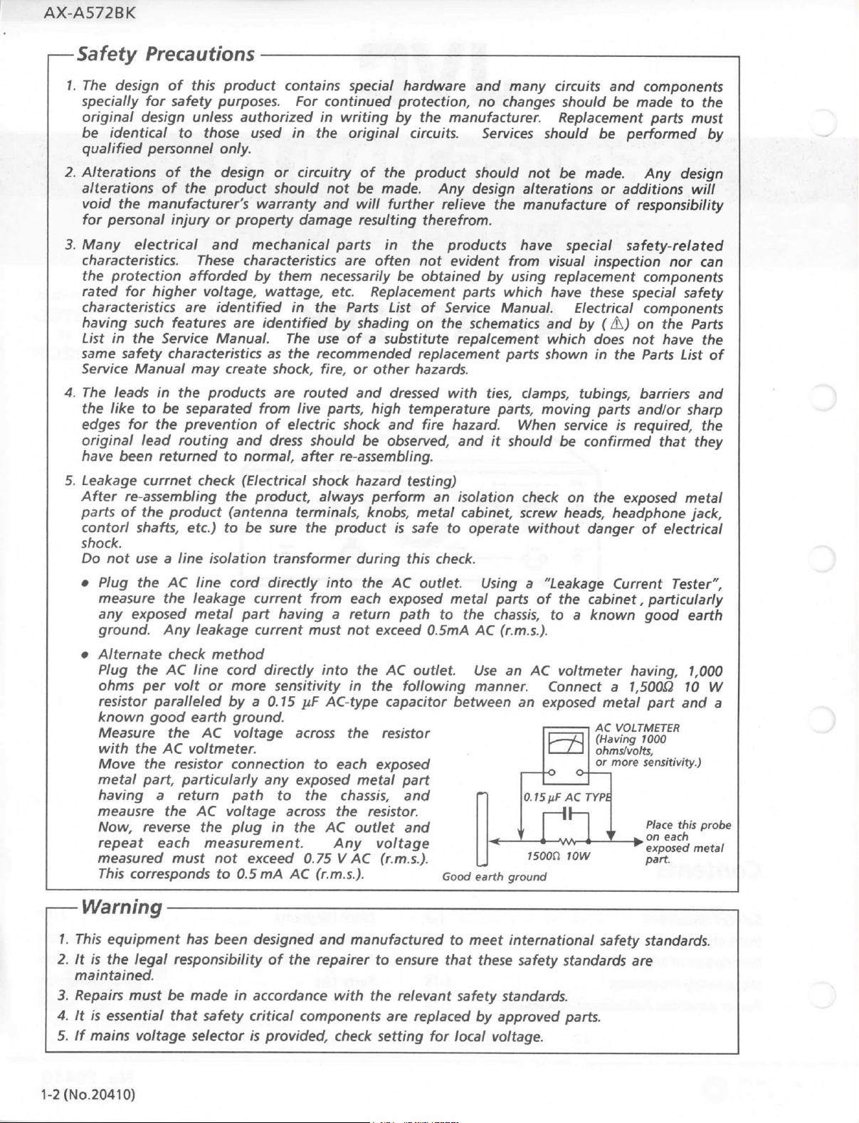
5. Leakage currnet check (Electrical shock hazard testing)
After re-assembling the product, always perform an isolation check on the exposed metal
parts
of the product (antenna terminals, knobs, metal cabinet, screw heads, headphone jack,
contori shafts, etc.) to be sure the product is safe to operate without danger of electrical
shock.
Do not use a
•
Plug
the AC
measure the leakage current from each exposed metal parts of the cabinet, particularly
any exposed metal part having a return path to the chassis, to a known good earth
ground. Any leakage current must not exceed
• Alternate check method
Plug
the AC
ohms per volt or more sensitivity in the
resistor
known good earth ground.
Measure the AC voltage across the resistor
with the AC voltmeter.
Move the resistor connection to each exposed
metal part, particularly any exposed metal part
having a return path to the chassis, and
meausre the AC voltage across the resistor.
reverse
Now,
repeat
each measurement. Any voltage
measured must not exceed 0.75 V AC
This
corresponds to 0.5 mA AC
line
isolation transformer during this check.
line
cord directly into the AC outlet. Using a "Leakage Current Tester",
0.5mA
line
cord directly into the AC outlet. Use an AC voltmeter having, 1,000
following
paralleled by a 0.15 jiF AC-type capacitor between an exposed metal part and a
the plug in the AC outlet and
(r.m.s.).
(r.m.s.).
AC
(r.m.s.).
manner. Connect a
AC VOLTMETER
(Having 1000
ohms/volts,
or
more
0.15
nF AC TYPl
i50on
10W
Good earth ground
1,500ü
10 W
sensitivity.)
Place this probe
^on
each
exposed
metal
part.
—
Warning
1.
This equipment has been designed and manufactured to meet international safety standards.
2. It is the legal responsibility of the repairer to ensure that these safety standards are
maintained.
3.
Repairs must be made in accordance with the relevant safety standards.
4.
It is essential that safety critical components are replaced by approved parts.
5. If mains voltage selector is provided, check setting for
1- 2
(No.2 0 4 1 0 )
local
voltage.
Page 3
AX-A572BK
Inst ruct ion
Book
Contents
IntroductionzyxwvutsrqponmlkjihgfedcbaZYXWVUTSRQPONMLKJIHGFEDCBA 1
About
This
Manual 1
Before
Installing
Names of Parts 2
Preparation
Connecting Stereo Equipment 3
Connecting Speakers 5
Connecting the Power Supply 6
Basic
Operation
Operating Procedure 7
Your
Amplifier
3
7
1
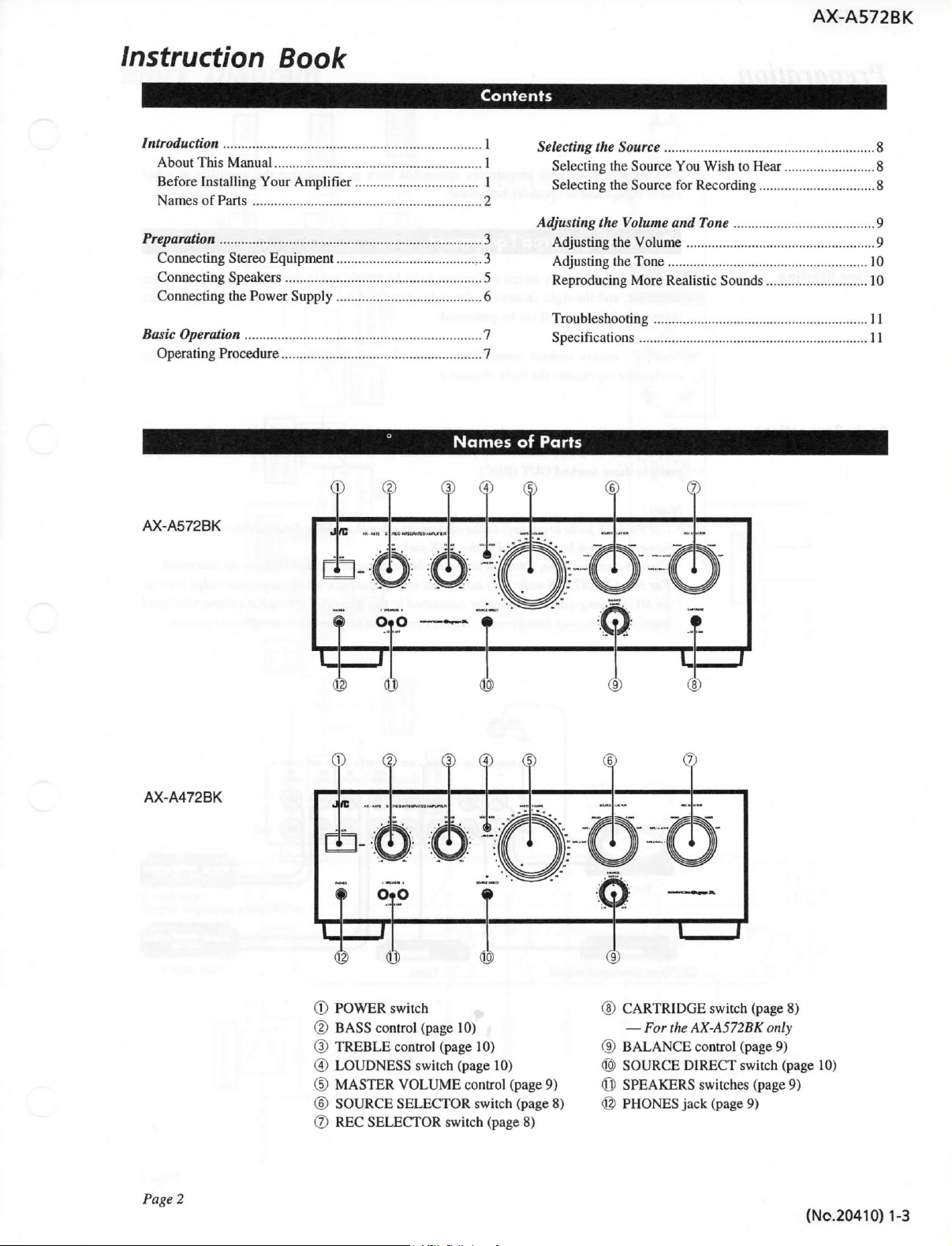
Names
(p
@
Selecting the Source 8
Selecting
Selecting
Adjusting the Volume and Tone 9
Adjusting
Adjusting
Reproducing More Realistic Sounds 10
Troubleshooting 11
Specifications
of
Parts
the Source You
the Source for Recording 8
the Volume 9
the Tone 10
11
Wish
to Hear 8
AX-A572BK
AX-A472BK
®
Ój)
Page
2
®
POWER
(D
BASS
(3)
TREBLE
® LOUDNESS
® MASTER VOLUME
(D
SOURCE SELECTOR
® REC SELECTOR
switch
control
control
(page
(page
switch
switch
10)
10)
(page
control
switch
(page
10)
(page
(page
8)
9)
8)
(D
CARTRIDGE
—
For the
(9) BALANCE
® SOURCE DIRECT
© SPEAKERS
@
PHONES
switch
AX-A572BK
control
switches
jack
(page
(page
only
(page
switch
(page
9)
8) zyxwvutsrqponmlkjihgfedcbaZYXWVUTSRQPONMLKJIHGFEDCBA
9)
(page
10)
9)
(No.20410)
1-3
Page 4
AX-A572BK
Preparation
Bef
ore
Starting
Basic
Connections
This
chapter
stereo
deals
with preparatory operations such as connecting the amplifier to other
equipment or speakers
before
use.
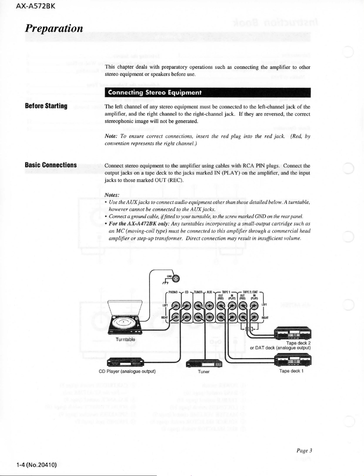
Connecting Stereo Equipment
The
left
channel of any
amplifier, and the right channel to the right-channel jack. If
stereophonic
Note:zyxwvutsrqponmlkjihgfedcbaZYXWVUTSRQPONMLKJIHGFEDCBA
image
To ensure correct connections, insert the red plug into the red jack. (Red, by
convention represents the right channel.)
Connect
output
jacks
stereo
jacks on a
to
those
equipment to the amplifier using cables with
marked OUT
stereo
equipment must be
will not be generated.
tape
deck to the jacks marked IN
(REC).
connected
(PLAY)
to the left-channel
they
are reversed, the correct
RCA
PIN plugs. Connect the
on the amplifier, and the input
jack
of the
Notes:
•
Use the A
UXjacks
to connect audio equipment other than those detailed below. A turntable,
however cannot be connected to the
•
Connect a ground
•
For the
AX-A472BK
an MC (moving-coil type)
amplifier
or step-up transformer.
cable,
only:
iffitted
to
Any turntables incorporating a small-output cartridge such as
must
r
PHONO
AUX
jacks.
yoiir
turntable,
to the screw marked GND on the rearpanel.
be connected to this amplifier through a commercial head
Direct
-V CD
connection may result in
-vTUNERv
AUX ^— WE1 —
OUT fN
(flffi)
(PLAY)
-TSPE2/DAT
OUT IH
(BEI
(PIAÏ)
or
DAT
insufficiënt
•
volume.
deck (analogue output)
Tape deck
2
1-4(No.20410)
CD P layer (analogue output)
Tuner
Tape deck
1
Page
3
Page 5
AX-A5 7 2BK
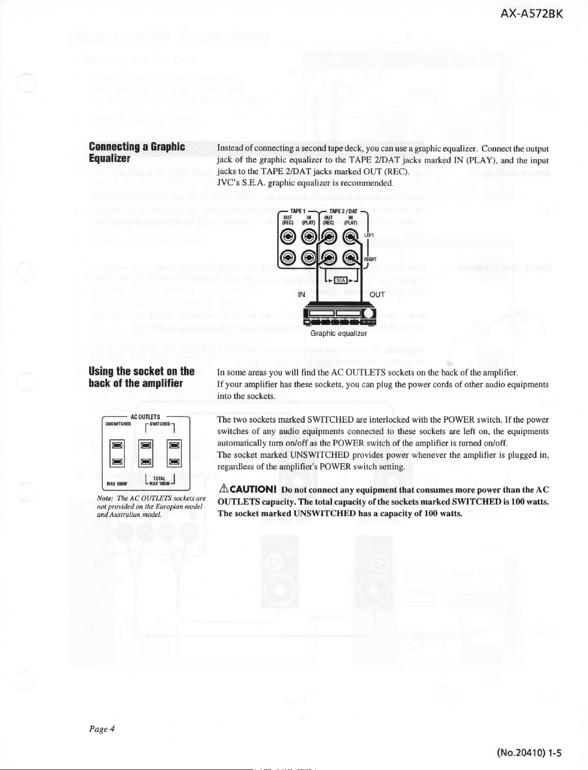
Conne cting a Graphic
Equalizer
Using the socl(et
bacl(
of the amplifier
ACOUTlfTS
UHSWIICH EO r SWITCHED-
SI
BI m m
MAXIOOW
Note:
The
provided
AC
on
nol
and Australian
on
| - SWITCHED-|
m m
I
TOTAL
OUTLETS
sockets
the
Europian
model.
the
are
model
Instead
of connecting a second
jack
of the
graphic equalizer
jacks
to the
TAPE
JVC's
S.E.A.
2/DAT
graphic equalizer is recommended.
to the
jacks
tape
deck, you can use a graphic equalizer. Connect the
TAPE
2/DAT
marked
OUT
jacks marked IN
(REC).
(PLAY),
and the
output
input
OUT
Graphic
equalizer
In
some areas you
If
your amplifier has
the
sockets.
into
The
two sockets marked
switches
of
automatically
The
socket marked
regardless of the amplifier's
ACAUTION!zyxwvutsrqponmlkjihgfedcbaZYXWVUTSRQPONMLKJIHGFEDCBA
OUTLETS
The
socket
will
find
the
AC OUTLETS
these
sockets, you can plug the power cords
SWITCHED
are interlocked
any audio equipments connected
turn on/off as the
UNSWITCHED
POWER
POWER
provides power whenever
switch
sockets
on the
back of the amplifier.
with
the
POWER
to
these
sockets
switch
of the amplifier is turned on/off
are
the
setting.
of
other audio equipments
switch.
left
on, the
amplifier
Do not connect any equipment that consumes more power than the
capacity.
marked
The
total
capacity
UNSWITCHED
of
the
sockets
marked
SWITCHED
has a capacity of 100 watts.
If the power
equipments
is
plugged in,
is 100 watts.
AC
Page
4
(No.20410)1-5
Page 6
AX-A572BK
Before
starting
Connecting
speakers
Connecting
Up
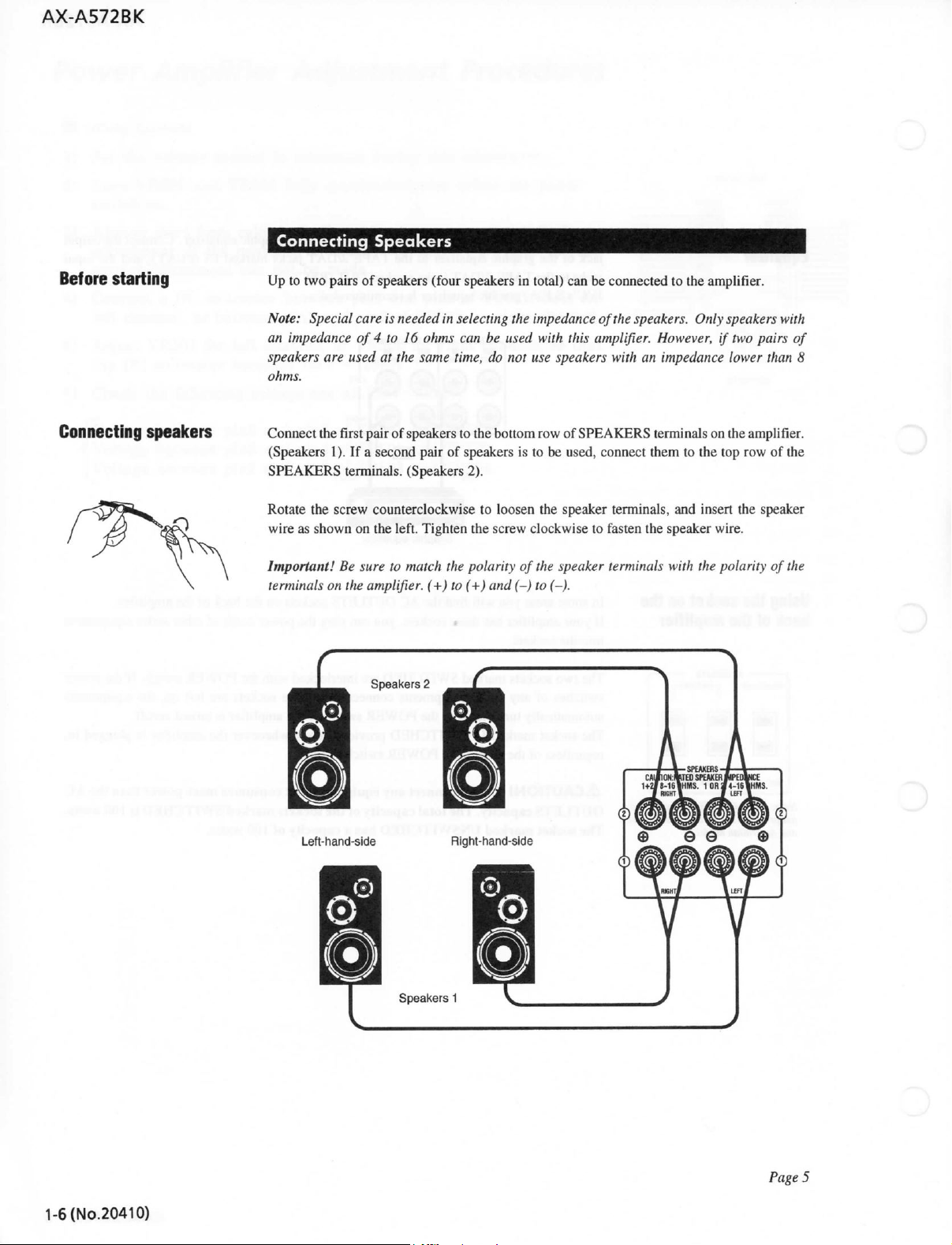
to two pairs of speakers (four speakers in total) can be connected to the amplifier.
Note:zyxwvutsrqponmlkjihgfedcbaZYXWVUTSRQPONMLKJIHGFEDCBA
Special
an impedance of 4 to 16 ohms can be used with this amplifier. However, if two
speakers
are used at the same time, do not use speakers with an impedance lower than 8
ohms.
Connect the
(Speakers 1). If a second pair of speakers is to be used, connect them to the top row of the
SPEAKERS
Rotate the screw counterclockwise to loosen the speaker terminals, and insert the speaker
wire
as shown on the left. Tighten the screw clockwise to fasten the speaker
Important!
terminals
on the amplifier.
Speakers
care
is needed in selecting the impedance
first
pair of speakers to the
terminals. (Speakers 2).
Be sure to match the polarity of the speaker terminals with the polarity of the
i+)to(+)
bottom
row of
and (-) to (-).
of
the speakers. Only speakers with
SPEAKERS
terminals on the amplifier.
wire.
pairs
of
1-6
(No.20410)
Page
5
Page 7
AX-A572BK
Bef
ore
starting
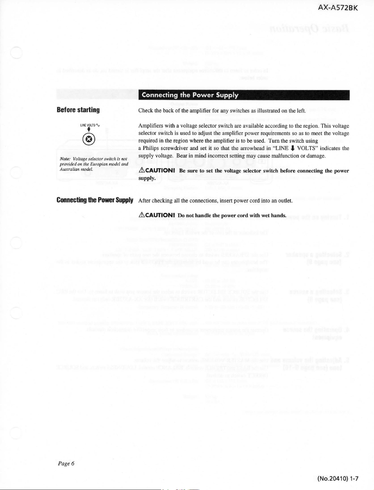
LINE
VOLTS
è
Note: Voltage selector
provided
on the
Auslralian
model.
Connec ting
the
switch
Europian
Power
is
model
not
and
Supply
ConnecHng
Check the back
Amplifiers
selector switch
required in the region where the amplifier is
a
Philips screwdriver and
supply voltage. Bear in mind incorrect setting may cause malfunction
ACAUTION!
supply.
After checking all the connections, insert power cord into an outlet.
ACAUTIONI
the
Power Supply
of
the amplifier
with a voltage
is
used
to
Be
sure
Do not handle the power cord with wet hands.
for
any switches
selector switch are available according
adjust the amplifier power requirements
set it so
to set
the
that
voltage
the
as
illustrated on the left.
to be
used.
arrowhead
selector switch before connecting
to
so
Turn
the switch using
in
"LINE ^ VOLTS"
,
the region.
as
to
meet the
or
damage.
This
voltage
voltage
indicates
the
power
the
Page
6
(No.20410)
1-7
Page 8
AX-A572BK
Basic
Operation
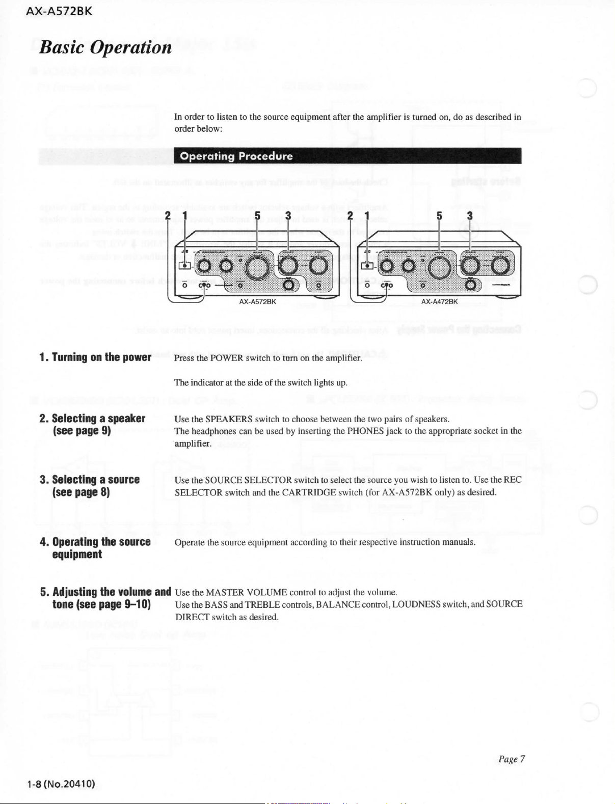
In
order to listen
order below:
Operating Procedure
to
the source equipment after the amplifier is turned on, do as described in
AX-A572BK AX-A472BK
1.
Turning
2.
Selecting a speaker
(see page 9)
3.
Selecting a source
(see page 8)
4.
Operating
equipment
5.
AdjUSting
tone
on the power
the source
the volume and
(see page 9-10)
Press the
The
Use
The
amplifier.
Use
SELECTOR
Operate the source equipment according to their respective instruction manuals.
Use
Use
DIRECT
POWER
indicator at the side of the
the
SPEAKERS
headphones
the
SOURCE SELECTOR
the
MASTER VOLUME
the
BASS
switch
switch
to tum on the amplifier.
switch
can be used by inserting the
switch and the
and
TREBLEcontrols,BALANCEcontrol,LOUDNESS
as desired.
switch
lights up.
to
choose between the two pairs of speakers.
PHONES
switch
to select the source you
CARTRIDGE
control to adjust the volume.
switch (for
jack
to
the appropriate socket in
wish
AX-A572BK
to listen to.
only)
as desired.
switch,
Use
the
and
SOURCE
the
REC
(No.20410)
1-8
Page?
Page 9
Selecting the Source
You
can select
connected to the amplifier.
Selecting
the
the
source you
Source
wish
You
to
hear
Wish
or
record from among
to
Hear
AX-A57 2BK
the
stereo equipment
Seiecting
You
Wish
Type
of
Turntable
Selecting
TAPE
1».
2/ D AT
the
to
SOURCE
the
REC
Source
Hear
SELECTOR
Source
SELECTOR
Use
TAPE
TAPEl:
PHONO:
CD:
TUNER:
AUX:
Cartridge
Use
For
set the gain of the
(moving
tridge, set the
because of
TAPE
TAPE 1 •
PHONO:
CD:
TUNER:
AUX:
the
SOURCE SELECTOR
2/DAT:
the
AX-A572BK
magnet) cartridge, set the
its
Selecting
the
REC SELECTOR
2/DAT
2/DAT:
Use this position to record from a record.
Use this position to record from a
Use this position to record from the radio.
Use this position
Use
Use
Use
Use
Use
Use
AUX
only: Before using the turntable, press the
phono
switch
to
high
output
the
Source
•
1: Use this position to record from the
Use this position to record from the
amplifier's
switch
to choose the source.
this position to listen to the
this position to listen to the
this position to listen to a record.
this position to listen to a
this position to listen to the radio.
this position
jacks.
equalizer to match the type of cartridge being used. For an
"«MC"
level,
for
switch
to
listen
switch
to
"MMM"
(depressed). If you
change the
switch
Recording
to select the source for recording.
to
record from
AUX
jacks.
tape
deck 2.
tape
deckzyxwvutsrqponmlkjihgfedcbaZYXWVUTSRQPONMLKJIHGFEDCBA 1.
CD.
to
equipment connected
(out). For an
detect
distortion
to the
MM
setting.
tape
deck 2 to the
tape
deck 1 to the
CD.
the
equipment connected
to the
CARTRIDGE
MC
(moving
with
an
MC
tape
tape
amplifier's
switch
and
MM
coil)
car-
cartridge
deck 1.
deck 2.
to the
Page
8
(No.20410)1-9
Page 10
AX-A572BK
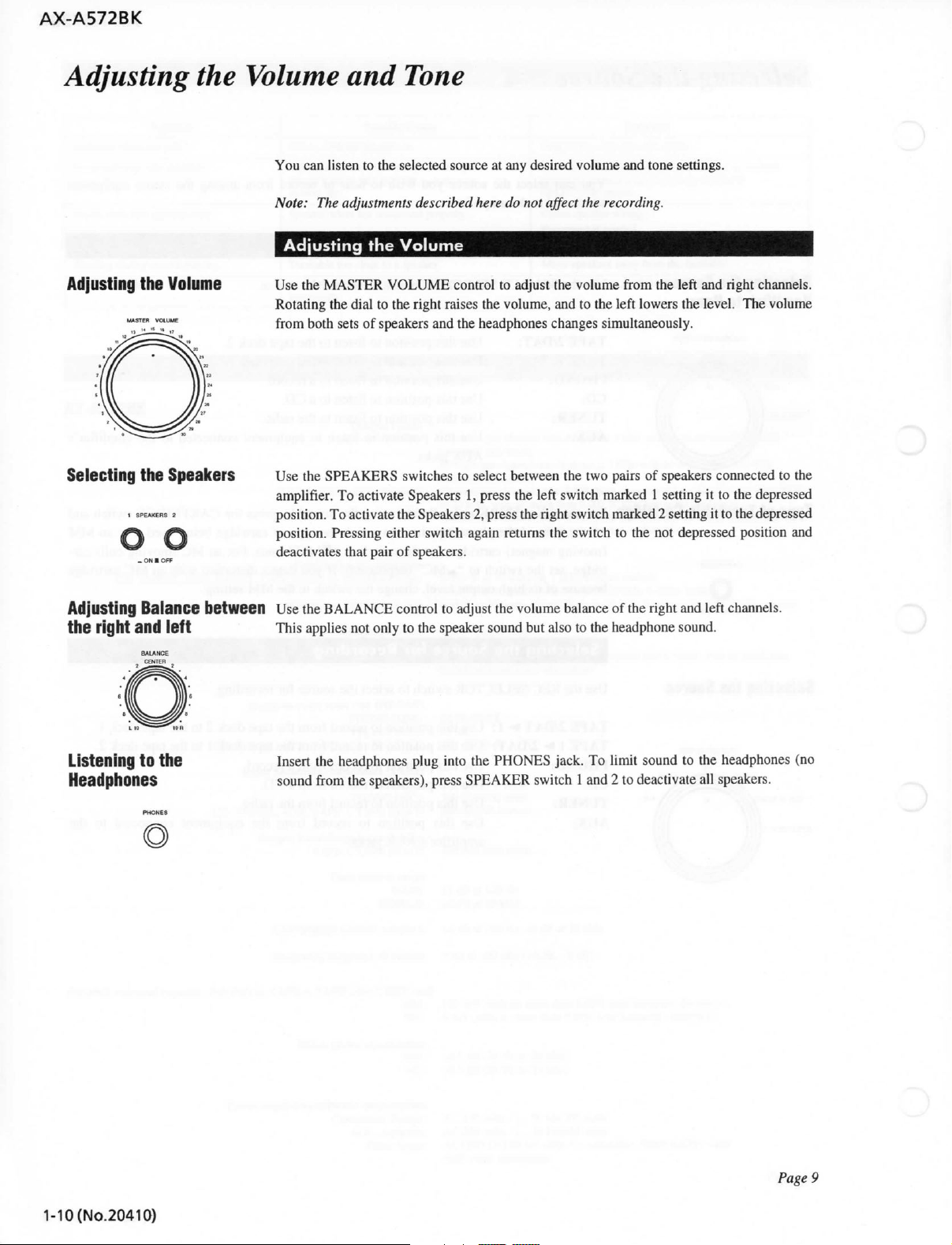
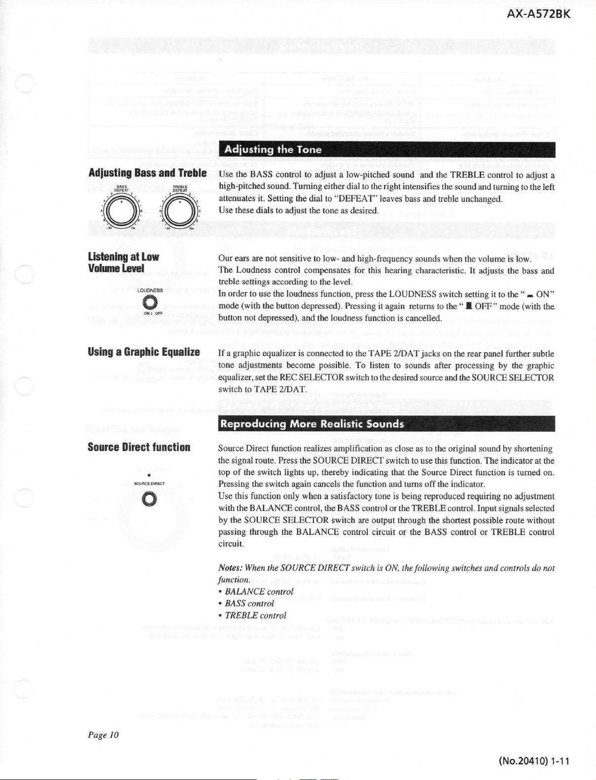
Adjusting the
Adjusti ng the
Selecting
Volume
MASTER
VOLUME
the
Speakers
SPEAKERSzyxwvutsrqponmlkjihgfedcbaZYXWVUTSRQPONMLKJIHGFEDCBA
2
Volume
You
can listen to the selected source
Note:zyxwvutsrqponmlkjihgfedcbaZYXWVUTSRQPONMLKJIHGFEDCBA
Adjusting
Use
the
Rotating the
ft-om both
Use
the
amplifier.
position.
position. Pressing either switch again returns
deactivates
and
The
adjustments
Tone
described
the Volume
MASTER VOLUME
dial
to
the right raises the volume, and to the left lowers the
sets
of speakers and the
SPEAKERS
To activate Speakers 1, press
To
activate the Speakers
that
switches
pair of speakers.
control
to
at
any desired volume and
here
do not
affect
the
to
adjust the volume from the left and right channels.
headphones
select between
2,
press the right
changes simultaneously.
the
two pairs
the
left switch marked 1 setting
switch
the
switch
tone
recording.
of
speakers connected
marked 2 setting it to the depressed
to the not
settings.
level.
The volume
it to the
depressed position
depressed
to the
and
Adjusting
the right
Listenlng
Balance
and
to the
Headphones
between
lelt
This
insert
sound from the speakers), press
Use
the
BALANCE
appUes not only to the speaker sound but also to the
the
headphones
control to adjust the volume balance
plug into
the
PHONES
SPEAKER
of
the right and left channels.
headphone
jack. To
switch 1 and 2 to deactivate
limit
sound
sound.
to the
headphones
all
speakers.
(no
1-10(No.20410)
Page
9
Page 11
AX-A572BK
Adjusting
Listening
Volume
Bass and
at Low
Level
Using a GraphiC
Treble
Equalize
Adjusting the
Use
the
BASS
high-pitched sound.
attenuates
Use
Our
The
treble settings according to the
In
order to use the loudness function, press the
mode
button not depressed), and the loudness function is cancelled.
If a graphlc equalizer
tone
equalizer, set the
switch
it. Setting the
these
dials to adjust the
ears are not sensitive to low- and high-frequency sounds when the volume is low.
Loudness control compensates for this hearing characteristic. It adjusts the bass and
(with
the button depressed). Pressing it again returns to the " M
adjustments become possible. To listen to sounds after processing by the graphic
to
TAPE 2/D
Reproducing
Tone
control to adjust a low-pitched sound and the
Tuming
REC SELECTOR
AT.
More
either
dial
to
"DEFEAT"
tone
as desired.
level.
is
connected to the
switch
Realistic
dial
to the right intensifies the sound and turning to the left
leaves bass and treble unchanged.
LOUDNESS
TAPE 2/D AT
to the desired source and the
switch
jacks
Sounds
TREBLE
on the rear panel further subtle
control to adjust a
setting it to the " . ON"
OFF"
SOURCE SELECTOR
mode
(with
the
Source
Direct
SOURCE DIRECT
function
Source
Direct function realizes amplification as close as to the original sound by shortening
the signal route. Press the
top of the
Pressing
Use
with
by
passing through the
circuit.
Notes:
function.
•
BALANCE
•
BASS
• TREBLE
switch
the
switch
this function only when a satisfactory
the
BALANCE
the
SOURCE SELECTOR
When the
control
SOURCE
control
control
SOURCE DIRECT
lights up, thereby indicating
again cancels the function and tums off the indicator.
control, the
BALANCE
BASS
switch
control
DIRECT
switch
switch
that
tone
is being reproduced requiring no adjustment
control or the
are
output
through the shortest possible
circuit
or the
is ON the following
to use this function. The indicator at the
the Source Direct function is tumed on.
TREBLE
BASS
control.
control or
switches
Input signals selected
TREBLE
and controls do not
route
without
control
Page 10
(No.20410)
1-11
Page 12
AX-A572BK
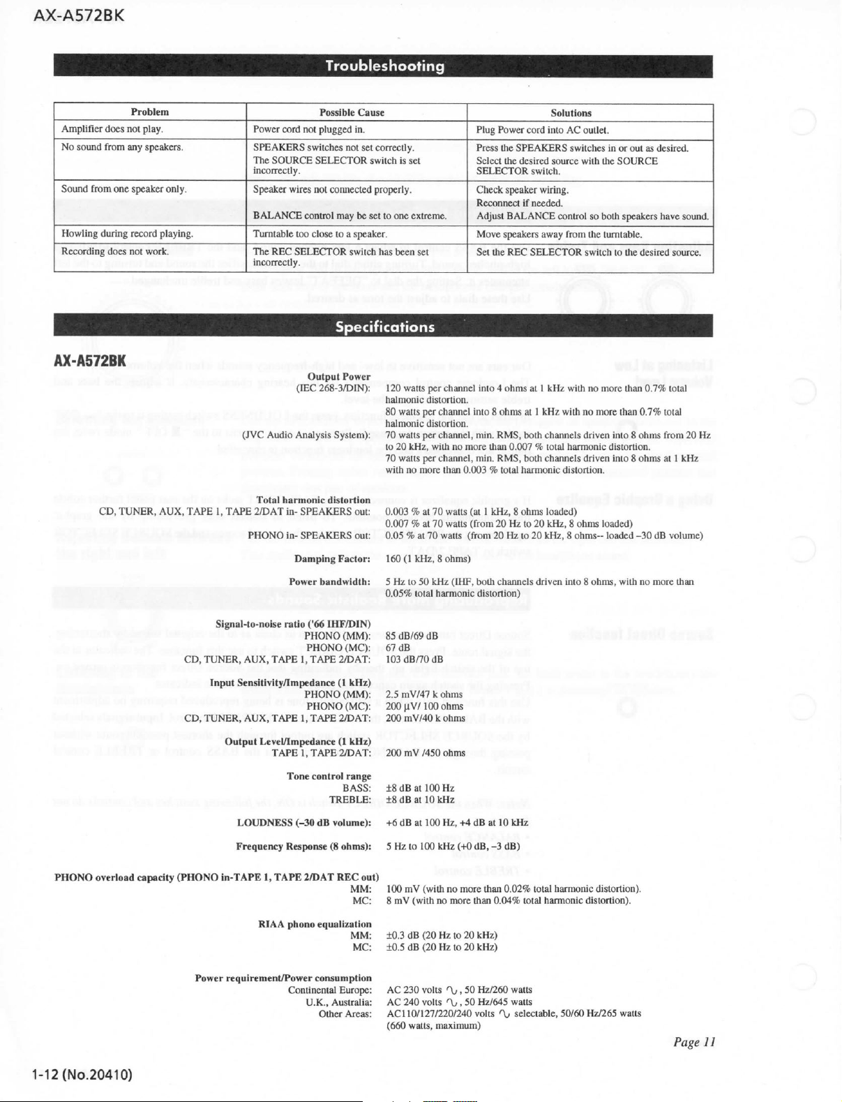
Troubleshooting
Problem
Amplifier
does
not play.
No
sound from any speakers.
Sound
from one speaker only.
Howling
during record playing.
Recording
does
not work.
AX-A572BK
CD, TUNER, AUX, TAPE
1,
Possible Cause
Power
cord not plugged in.
SPEAKERS
The SOURCE SELECTOR
incorrectly.
Speaker
BALANCE
Tumtable
The REC SELECTOR
incorrectly.
switches not set correctly.
wires
not connected properly.
control may be set to one extreme.
too close to a speaker.
switch
switch
is set
has been set
Specifications
Output
Power
(lEC
268-3/DIN):
.
80 watts per channel into 8 ohms at 1 kHz
(JVC
Audio
Analysis
Total
TAPE
harmonie distortion
2/DAT
in-
SPEAKERS
PHONO
in-SPEAKERS
Damping
Power
bandwidth: 5 Hz to 50 kHz
120 watts per channel into 4 ohms at 1 kHz
halmonic
distortion.
halmonic
System):
70 watts per charmel, min.
out:
out:
Factor: 160 (1 kHz, 8 ohms)
distortion.
to 20
kHz,
with
70
watts per channel, min.
with
no more than 0.003 % total harmonie distortion.
0.003 % at 70 watts (at I kHz, 8 ohms loaded)
0.007 % at 70 watts
0.05 % at 70 watts
0.05%
total harmonie distortion)
no more than 0.007 % total harmonie distortion.
(from
(from
(IHF,
Solutions
Plug
Power cord into AC outlet.
Press
the
SPEAKERS
Select
the desired source
SELECTOR
Check
speaker
Reconnect
Adjust
Move
Set
both channels driven into 8 ohms,
if
BALANCE
speakers away from the tumtable.
the
REC SELECTOR
RMS,
both chaimels driven into 8 ohms from 20 Hz
RMS,
both channels driven into 8 ohms at 1 kHz
20 Hz to 20
20 Hz to 20 kHz, 8 ohms- loaded -30 dB volume)
switches in or out as desired.
with
the
switch.
wiring.
needed.
control so both speakers have sound.
with
with
kHz,
8 ohms loaded)
SOURCE
switch
to the desired source.
no more than 0.7% total
no more than 0.7% total
with
no more than
PHONO
overload capacity
Signal-to-noise ratio ('66
CD, TUNER, AUX, TAPE
Input
Sensitivity/Impedance (1 kHz)
CD, TUNER, AUX, TAPE
Output
Level/Impedance (1 kHz)
LOUDNESS
Frequency
(PHONO
in-TAPE
Power
1,
RIAA
requirement/Power consumption
IHF/DIN)
PHONO
(MM)
PHONO
1,
1,
TAPE
1,
Tone
(-30 dB volume):
Response (8 ohms):
TAPE
phono
Continental
(MC)
TAPE
2/DAT
PHONO
(MM):
PHONO
(MC)
TAPE
2/DAT:
TAPE
2/DAT:
control range
TREBLE:
2/DAT
REC
equalization
Europe: AC 230 voltszyxwvutsrqponmlkjihgfedcbaZYXWVUTSRQPONMLKJIHGFEDCBA
U.K.,
Australia:
Other
Areas;
85
dB/69
67
dB
103
dB/70
mV/47
2.5
200
HV/100
200
mV/40
200
mV /450 ohms
±8 dB
BASS:
out)
MM;
MC;
MM: ±0.3
MC: ±0.5 dB (20 Hz
at
at
±8 dB
+6
dB
at 100
Hz to 100
5
100 mV
8 mV
(with
dB
(20 Hz
AC 240 volts %, 50
AC110/127/220/240
(660
watts, maximum)
dB
dB
k ohms
ohms
k ohms
100 Hz
10 kHz
Hz, -h4 dB
kHz
(with
no more than 0.04% total harmonie distortion).
at 10
kHz
(+0
dB,
-3
dB)
no more than 0.02% total harmonie distortion).
to 20
kHz)
to
20 kHz)
"XJ
, 50
Hz/260
watts
Hz/645
watts
volts % selectable, 50/60
Hz/265
watts
Page
11
1-12(No.20410)
Page 13

AX-A572BK
•szyxwvutsrqponmlkjihgfedcbaZYXWVUTSRQPONMLKJIHGFEDCBA
i
AX-A472BK
CD, TUNER, AUX, TAPE
Dimensions (W X H X
(JVC
Audio
Total
harmonie distortion
1,
TAPE 2/DAT in-SPEAKERS
PHONO
in-SPEAKERS
Signal-to-noise ratio ('66
CD, TUNER, AUX, TAPE
Input
Sensitivity/Impedance (1 kHz)
CD, TUNER, AUX, TAPE
Output
Level/Impedanee (1 kHz)
TAPE
Output
(lEC
268-3/DIN):
Analysis
Damping
Power
bandwidth:
IHF/DIN)
PHONO
1,
TAPE 2/DAT:
PHONO
1,
TAPE 2/DAT:
1,
TAPE 2/DAT:
D):
435 x 148 x 355.5 mm
17-3/16x3/16x14-1/16
Weight:
Power
System);
Factor:
(MM):
(MM):
10.0
22.1
90
halmonic
65
halmonic
55watts per channel, min.
to 20 kHz,
55
with
0.003 % at 55 watts (at 1 kHz, 8 ohms loaded)
out:
0.007 % at 55 watts
0.05 % at 55 watts
out:
160(1
5
Hz to 50 kHz
0.05%
76
103
2.5
200
200
inches
kg
Ibs
watts per channel into 4 ohms at 1 kHz
distortion.
watts per channel into 8 ohms at 1 kHz
distortion.
with
watts per channel, min.
no more than 0.003 % total harmonie distortion.
dB/69
dB/70
mV/47
mV/40
mV /450 ohms
no more than 0.007 % total harmonie distortion.
kHz, 8 ohms)
total harmonie dis tortion)
dB
dB
k ohms
k ohms
(from
(IHF,
RMS,
both channels driven into 8 ohms from 20 Hz
RMS,
(from
20 Hz to 20
20 Hz to 20
boUi
channels driven into 8 ohms,
with
no more than 0.7% total
with
no more than 0.7% total
bolh channels driven into 8 ohms at 1 kHz
kHz,
8 ohms loaded)
kHz,
8 ohms- 1 oaded
-30 dB volume)
with
no more than
PHONO
overload capacity
(PHONO
Power
Tone
control
TREBLE;
LOUDNESS
Frequency
In-TAPE
requirement/Power consumption
(-30 dB volume):
Response (8 ohms):
1,
TAPE
2/DAT
REC
RIAA
phono
equalization: ±0.3 dB (20 Hz to 20 kHz)
Continental
Dimensions (W x H XD): 435 x 148 x 355.5 mm ^
Europe: AC 230 volts % , 50
U.K.,
Australia:
Other
Areas:
Weight: 9.0 kg
range
BASS:
±8 dB at 100 Hz
±8 dB
+6
dB
5 Hz
to 100
out): 100 mV
AC 240 volts % , 50
ACl
10/127/220/240 volts % selectable, 50/60
(585
watts, maximum)
17-3/16X3/16X
19.9
Ibs
at
10 kHz
at
100 Hz,
+4
dB
at 10
kHz
kHz
(+0
dB,
-3
dB)
(with
no more than 0.02% total harmonie distortion).
Hz/225
watts
Hz/540
watts
14-1/16inches -.-.-3 • : ,.
Design and
specifications
Hz/230
watts
subject to cliange
witliout
notice.
Page
12
(No.20410)
1-13
Page 14
AX- A57 2 BK
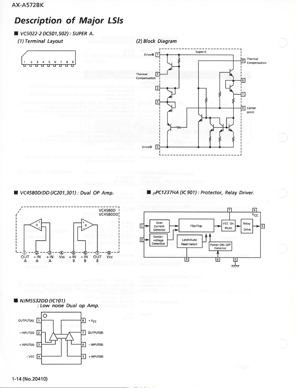
Description
IzyxwvutsrqponmlkjihgfedcbaZYXWVUTSRQPONMLKJIHGFEDCBA
VC5 0 22- 2
(1)
Terminal Layout
/
1
UUUUUUUUU
(IC5 0 1,5 0 2) : SUPER
2 34 567 89 zyxwvutsrqponmlkjihgfedcbaZYXWVUTSRQPONMLKJIHGFEDCBA
of
Major
A.
LSIs
{2)
Block Diagram
Drive©
[T
Ther mal
[T}
Comp ensation
Drivee
[?]•
Ther mal
Comp ensation
VC458 0 D/ DD
1__
OUT
- IN + IN Vss + IN - IN OUT Vcc
A
A A B B B
(IC2 0 1,3 0 1) : Dual
NJM553 2 DD (IC1 01)
Low
OUTPUT(A)
-
INPUT(A)
:
| T
\T_ —
no/ se Dual
op Amp.
1]
+ vcc
7]
OUTP UT( B)
OP Amp.
VC45 8 0D
VC45 8 0DD;
H
[ I
pPCI23 7 HA
Over
Curren t
Det ector
Center -
voltag e
Det ectlon
(IC 90 1 ):
Flip- Flop
Latch/ Auto
l^eset Select
UT
Protector. Relay Driver.
JU
Vcc
Relay
Drive
Power
Det ector
vcc
Mut e
ON/ Off
On
Tl T
3
.6 ]
+
INPUT(A)
[T_
- vcc
[T
1- 14 (No.2 041 0 )
ë] -INPUT(B )
7]
+INPUT(B)
Page 15

Disassembly Procedures
1.
Removing the Top Cover
AX-A572BK
1) Remove
both
the 3 screws fastening
2) Remove
the
sides
the Top
4 screws fastening
of
the
Top
Cover,
the
Cover.
2. Removing the Front Panel
1) Remove
top
fastening
2) Remove
SOURCE
3) Remove
3.
Service procedures of Main PCB
1) Remove
2) Remove
3) Cut
4) Remove
5) Slide
6) Remove
7) Remove
8) Separate
rear
in
the
of
the Front
bottom
the 6
SELECTOR
the
the 12
the
the
Tie Band
the 4
the
Trans
the
the 6
the
panels from
fïg-4.
plastic ribet ® fastening
Panel,
knob
and
of
the Front Panel.
(MASTER
etc).
Front Panel.
screws
©,©
wire clamp © and
®.
screws fastening
to
arrow direction
wire clamp
screws
Main PCB
the
®.
® on the
with
chassis base
and
rear sides.
the 3
screws
VOLUME,
and
©.
©.
the
Trans.
®.
Main PCB.
the
front and
as
shown
(NOTE)
1)
Take care not to short-circuit
the
filter condenser C811 and C812.
2)
Wire should be set as Fig-5.
Front Panel, Main PCB
&
Rear panel
fig-4
p
'O'O
O O O O O
O O O O
op op zyxwvutsrqponmlkjihgfedcbaZYXWVUTSRQPONMLKJIHGFEDCBA
ooob
fig-3
Tie
Band®
Wier
Clamp®
REAR
fig-5
(No.20410)1-15
Page 16

AX-A572BK
Power
•
Idling
1) Set the volume control to minimum during
2)
Turn
3) Always
4) Connect a DC voltmeter between
5) Adjust
6) Check the following voltage are all 7mV~15mV.
<
Amplifier
Current
VR501
switch
adjustment.
correct adjustment can not be made.
left
channel, or between
the DC voltmeter
fVoltage between pin2 and pin3 of
Voltage between pin2 and pin4 of
Voltage between
and VR502
on.
start
from cold, and allow 10 minutes to warm up
If the heatsink is already warm from previous use the
VR501
for left channel, or VR502 for right channel, so that
pinl
Adjustment Procedures
fully
counterclockwise
pinl
pinl
and pin2 of TP502 for right channel.
becomes
7mV ~ 15mV.
TP501
TP501
and pin2 of TP503 and TP504.
this
and pin2 of
and
TP502.
and
TP502.
adjustment.
before
the power
TP501
before
leads for
(No.20410)
1-16
Page 17

Block Diagram
/o
O z O
I
O.
1--^
/o /o
O
0
^o|
(No.20410)
1-17
AX-A572BK
Page 18

AX-A572BK
-MEMO-
1-18{No.20410)
Page 19

r.
C
AX-A572BK
-MEMO-
C
C
c
(No.20410)
1-19
Page 20

Page 21

• Pre Driver PC Board (ENG-011)
AX-A572BK
(No.204 1 0 )
Page 22

AX-A572BK
• Power Supply PC Board (END-092)
(For TAIWAN, OTHER COUNTRIES)
(No.
2 0 4 10)
Page 23

Page 24

Page 25

PARTS LIST
AX-A5 7 2BK
Note
: AU
p rinte d circuit boards and its
Contents
General
Printed Circuit Board Ass'y
Accessories
Packing M aterials
Exploded View
• ENH- 2 2 5 n
•
ENG- OnD Pre
• END- 0 9 2 [B]
Amplifier, Selecor & Power Supply
Power Supply
List
2 - 1 3
and
and
Parts List
and
Parts List
Driver
PC
Board
PC
Part Num bers
assemblies
2 - 2
2 - 7
2 - 1 1
Board
2 - 1 2
2 - 1 4
are not available as service p arts.
PC
Board
2 - 7
(No.
20410)
2-1
Page 26

AX-A572BK
2-2 (No. 20410)
Page 27

Page 28

AX-A57 2 BK
•
Parts List
Item Part Number
1
1-1
1-2 El
1-3
1-4
1-5
1-6
1-7
1-8
2
3
4
5
6
7
8
9
10
11
12
13
14
15
16
17
18
19
20 El
21
22
23
24
25
26
27
28
29
30
31
32
33
34
35
A
Part Name
EFP-AXA572BK E(S
02703-005
El
02704-002
E407511-001
E407750-001
E407553-001
E407766-001
E60912-003
E72968-001
E308095-002
E308096-009
E308097-005
E308137-007 BALANCEKNOB
SDSG3008CC
SDSG3008CC
SDSG3008CC
E48729-009 PLA STIC RI VET
E406481-004 PUSH BUTTON
E407110-002 PUSH BUTTON
E407321-002SM PUSH BUTTON
El
02705-002
GBSG3006CC
GBSG3006CC
GBSG3006CC
E73273-O03
SBST3006CC
E407111-001
QSR2B16-E01
QSR2B16-E02 ROTARY SWITCH
E407336-001
E68587-002 BRACKET
02702-001
E72018-001
E72018-003 WIR ECLAMP
E303704-001
E303704-002 WIRECLAMP
E307427-004 FOOTASSY
E307427-005zyxwvutsrqponmlkjihgfedcbaZYXWVUTSRQPONMLKJIHGFEDCBA
GBST3008CC SCREW
E308492-001 HEATSINK
E73525-003 SCREW
WNS3000CC WASHER
E308496-001 HEA TSINKBRACKET
E26269-012
E26269-013
E61660-004
E306233-O02
E308493-001
E407337-001
ETP1150-50EA
t
FRONT PANEL ASSY
FRONT PANEL
FRONT BASE
INDICATOR LENS
SHEET
INDICATTOR LENS
SHEET
SPEED
NUT
JVC
MARK
VOLUME K NOB
SELECT KNOB
TONEKNOB
SCREW
SCREW
SCREW
FRONT BRACKET
SCREW
SCREW
SCREW
SPECIAL SCREW
SCREW
HEADPHONEBRA CKET
ROTARY SWITCH
VOLUME B RACKET
CHASSIS BASE
WIRECLAMP
WIRECLAMP
FOOTASSY
" .-^
MET AL COVER
MET AL COVER
SCREW
PROTECTSHEET
PUSH SHAFT
SPACER
POWER TRANSFORMER
Q'ty
1
1
1
1
1
1
1
1
1
1
2
2
1
3
POWER
1
SORUCE,SPEAKER
1
LOUDNESS
1
48
49
51
7
5
1
1
1
2
1
1
1
1
1
4
4
4
2
8
8
2
1
1
4
1
1
MQMM
4
1
Description
ï
ï
' f- ,
' f- ,
Area
U
UT
EN,EF,A
G
U.UT
Except
U,UT
U.UT
Except EF,EN,G
EF,EN,G
•
Except
A,G
A,G
Except
U,UT
2-5 (No.
20410)
Page 29

Item
A
A
36
37 E407512-001
38 QMF51E2-3R15J1
A
39 E307572-001
40
A
A
41 E308494-002
42 QMF51E2-2R5J1
A
43 E207833-001
44
45 EXO150010N20S
46
A
47 QMP25F0-244
A
A
A
48
49
50 E71862-001
51
52 E48729-008 PLASTIC RIVET Except U,UT
53
54 E306805-096 SPACER 1
55
56 E306805-095
57
58
59
-
-
- E70027-O01
-
-
Part Number Part Name
ETP1150-50FA
E61661-003
Q1V1F51E2-5R0J1
QMF51E2-5R0J1
E207833-002
E207833-003
E70078-003
QHS3876-162
QMP3900-200
QMP7520-200
E306805-092 SPACER 3
EXO020010R10S10
E407735-001
E74266-002 SCREW 1
E306805-093
E308522-030
2SC3854LD(O.P.Y) TRANSISTOR
2SA1490LD(O.P.Y) TRANSISTOR 4
E61029-005
E67000-005
QZL1031-101
E407619-005
QZLI007-001
POWER TRANSFORMER 1
SPECIAL SCREW
BUTTON BRACKET
FUSE
FASTNER 1
FUSE
FUSE 1
PUSHSHAFT > 1 POWER
FUSE
RE AR PANEL 1
RE AR PANEL 1
RE AR PANEL
GND TERMINAL
SPACER
CORD STOPPER
POWER CORD 1
POWER CORD
POWER CORD
SPACER
VOLUME NUT
PROTECTOR COVER
SPACER 1
SPACER 1
RATING LABEL ' | ,
NUMBER LABEL
CAUTION LABEL
LABEL 1
LABEL
FTZLABEL
LABEL
Q'ty
4
1
1 Except U,UT
1
1 U,UT
1
1
1
1
1
1 U,UT
1
1
1
1 UT
0511,512,515,516 UT
0513,514,517,518 UT
1
1
1 EN
1
Description Area
...
U,UT
Except U,UT
U
UT
A,
EF,EN,G
U,UT
A
EF,EN,G
Except U,UT
EF
G
A : Safety Parts
The Marks for Designated Areas
A Australia EF Scandinavia EN Continental Europe
G Germany U UnIversaI Type UT Taiwan
No mark indicatesall
area.
2-6 (No. 20410)
Page 30

Printed Circuit Board Ass'y and Parts List
• ENH-225• Amplifire, Selector & Power Suplly PC Board
Note:
ENH-225
• varies according to the areas employed. See note (1) when placing an order.
AX-A572BK
Q
1 fï" '-^1 lis 4~> ^ cM<c3 .p n r
(No.
20410) 2-7
Page 31

AX-A572BK
Noted)
PC
Board Ass'y
ENH-225
ENH-225
ENH-225
ENH-225
Transistors
ITEM
PART NUMBER
QlOl
Q102
Q103
Q104
Q105
G106
Q361
Q362
Q501
Q502
Q5Ö3
0504
Q505
Q506
QSC7
Q508
Q509
Q510
Q519
Q52Ö
Q521
Q522
Q523
0524
G601
Q611
Q821
Q822
Q823
Q824
Q901
Q902
Q903
I.C.S
ITEM
ICIOI
ICIOI
IC201
IC201
IC301
IC301
IC501
IC501
IC502
IC502
ÏC9Öi'
ÏC9Öi'
Diodes
ITEM
A
D119
0341
D361
0362
0501
D502
0511
0512
D513
D514
D602
D612
D801
0802
D803
[ÏÏI
\G\
[F]
Q]
Designated
Australia
Scandinavia
Continental
Germany
UniversaI
Type
Areas
Europe
Taiwan
DESCRIPTION
2SK170(BL)
2SK170(BL)
2SK170(BL)
2SK170<BL>
2SC1740S(R,S)
2SC174ÖS(RrS)
2SC2240CGR,BL)
2SC2240(GR,BL)
2SD637<Q,R)
2SD637<Q,R)
2SC224Ö(GR;BL)
2SC2240(GRrBL)
2SA970<GR,BL)
2SA970(GR,BL)
PT132
2SD669A(B,C)
2SB649A<B/C)
2SB649A(B^C>
2SK170CBL)
2SK17b(BL)
2SC1740S(R,S)
2SC1740S(R^S)
2SA933S<R,S)
2SA933SCR,S)
•2SC224Ö(GRrBL)
2SC2240(GR^BL)
2SD2061<FrG)
2SB1187<F,G)
2SK246<QR>
2S<246(GR)
2SC2389CS,E)
2SC2389(S^E>
2SA970CGR^BL)
PART NUMBER DESCRIPTION
NJM5532D0
VC4580D0
VC45800
VC5022-2
VC5022-2
UPC1237HA
PART NUMBER DESCRIPTION AREA
RD4.7JSB3
SLR-342YC3F
MTZ5.6JC
MTZS.6JC
1SS119
1SS119
1SS119
1SS119
1SS119
1SS119
1SS147
1SS147
30DF2SFC
300F2SFC
30DF2SFC
F.E.T
F.E.T
F.E.T
F.E.T
SILICON
SILÏCÓN
SILICON
SILICON
SILICON
SILICON
SILICON
SILICON
SILICON
SILICON
SILICON
SILICON
SILICON
SILICON
F.E.T
F.E.T
SILICON
SILICON
SILICON
SILICON
SÏLÏCON
SILICON
SILICON
SILICON
F.E.T
F.E.T
SILICON
SILICON
SILICON
I.C.
DAINICHI
I.C.
DAINICHI
I.C.
DAINICHI
I.C.
SANYO
I.C.
SANYO
I.C.
NEC
ZENER
L.E.D.
ZENER
ZENER
SILICON
SILICON
SILICON
SILICON
SILICON
SILICON
SILICON
SILICON
SILICON
SILICON
SILICON
TOSHIBA
TOSHIBA
TOSHIBA
TOSHIBA
ROHM
RÓHM
TOSHIBA
TOSHIBA
MATSUSHITA
MATSUSHITA
TOSHIBA
TOSHIBA
TOSHIBA
TOSHIBA
HITACHI
HITACHI
HITACHI
TOSHIBA
TOSHIBA
ROHM
ROHM
ROHM
ROHM
TOSHIBA
TOSHIBA
ROHM
ROHM
TOSHIBA
TOSHIBA
ROHM
ROHM
TOSHIBA
A i: ÏSlAiFiÉlTiyi :PiA;RiTi"$;
A iTISlAÏFiEiTiYi' IPiAl
NEC
ROHM
ROHM
ROHM
HITACHI
HITACHI
HITACHI
HITACHI
HITACHI
HITACHI
ROHM
ROHM
NIHONINTER
NIHONINTER
NIHONINTER
A iTSjaFiiiTjvripiAiMï
AREA
Diodes
ITEM PART
D804
30DF2SFC
D822
MTZ9.1JC
D823
RD1SJSB3
D824
R018JSB3
0825
MTZ20JC
0826
MTZ2ÖJC
0841
ERA15-02L19
0842
MTZIOJC
0851
SLR-34DC50F124
1SS119
0901
1SSÏ19
D9Ö2
1SS119
0905
Capacitors
ITEM
A
A
A
A
PART NUMBER DES C R P T I 0 N
COOl
QCZ9050
COOl
QCZ9050
COOl
QCZ9050
ClOl
QCS21HJ
C102 aCS21HJ
C1C5 aCS21HJ
Cl
06
QCS21HJ
C107 QFVBIHJ -103N
C108 QFVBIHJ -103N
C109
QFN81HJ
CllO
QFN81HJ
QCS21HJ
cm
C112
QCS21HJ
C119 EETBIHM
C121
EET0606
C122
EET0606
C131
QFN81HJ
C132
SFNSIHJ
C133
QFP81HJ
C134 SFP81HJ
C135 QFVBIHJ -153N
C136 QFVBIHJ -153N
0FN81HJ
C137
C138
QFN81HJ
C141
EET5006
C142
EET5006
C145 EETBICM -107E
C146 EETBICM
C147
QCS21HJ
QCS21HJ
C148
C151
QCS21HJ
C1S2
QCS21HJ
C153
QCS21HJ
C154 aCS21HJ
QCS21HJ
C155
C156
QCS21HJ
C157
QCS21HJ
C158
QCS21HJ
C159
QCS21HJ
C160
QCS21HJ
C161
QCS21HJ
C162
QCS21HJ
C163
QCS21HJ
C164
QCS21HJ
C171 QFVBIHJ
C172
aCVBlCM
C201
EETBIHM -225E
C202 EETBIHM -225E
C205 EETBICM
C20é EETBICM
C207
QCSBIHJ -470 47PF
C208
QCSBIHJ -470 47PF
C209
aCBBlHK
C210 SCBBIHK
C211
QFN81HJ
C212
QFN81HJ
C213 QFVBIHJ
C214 QFVBIHJ
C301
QFVBIHJ
C302
QFVBIHJ -105N IMF
C305
QCS21HJ
C306
QCS21HJ
C311
EETBIHM
EETBIHM
C312
C313 EETBIHM -106E
C314 EETBIHM -106E
C31S EETBIHM
C316
EETBIHM -225E
C321
QFVBIHJ
C322 QFVBIHJ -153N
NUMBER
-103A
-103A
-103A
-101
-101
-101
-101
-822 8200PF
-822
-101
-101
-476E
-227E
-227E
-472 4700PF
-472
-331
-331
-272 2700PF
-272
-475E
-475E
-107E
-221
-221
-101
-101
-101
-101
-101
-101
-101
-101
-101
-101
-101
-101
-101
-101
-103N
-103
-107E
-107E
-221
-221 220PF
-471
-471
-563N
-563N
-105N IMF
-100 iÖPF
-100
-106E
-106E
-225E
-153N
DESCRIPTION AREA
SILICON
ZENER
ZENER
ZENER
ZENER
ZENER
SILICON
ZENER
L.E.0.
SILICON
SiLÏCÓN
SILICON
O.OIMF
O.OIMF
O.OIMF
lOOPF
lOOPF
lOOPF
lOOPF
O.OIMF
O.OIMF
8200PF
lOOPF
lOOPF
47MF SOV
220MF
220MF
4700PF
330PF
330PF
0.015MF
0.015MF
2700PF
4.7MF
4.7MF
lOOMF
lOOMF
220PF
220PF
lOOPF
lOOPF
lOOPF
lOOPF
lOOPF
lOOPF
lOOPF
lOOPF
lOOPF
lOOPF
lOOPF
lOOPF
lOOPF
lOOPF
O.OIMF
O.OIMF
2.2MF
2.2MF
lOOMF
lOOMF
220PF
470PF
470PF
0.056MF
0.056MF
lOPF
lOMF
lOMF
lOMF
lOMF
2.2MF
2.2MF
0.015MF
0.015MF
NIHONINTER
ROHM
NEC
NEC
ROHM
ROHM
KYOUDOU
ROHM
ROHM
HITACHI
HITACHI
HITACHI
A iTISÏ ftFiElT iraeiAiSjïïSi
CERAMIC
CERAMIC
CERAMIC
50V
CERAMIC
50V
CERAMIC
50V
CERAMIC
50V
CERAMIC
50V
T.FILM
50V
T.FILM
SOV MYLAR
MYLAR
50V
SOV
CERAMIC
SOV
CERAMIC
ELECTRO
6.3V
ELECTRO
ELECTRO
6.3V
SOV MYLAR
SOV MYLAR
POLY
SOV
SOV
POLY
SOV
T.FILM
SOV
T.FILM
SOV MYLAR
SOV MYLAR
SOV
ELECTRO
ELECTRO
SOV
16V
ELECTRO
16V
ELECTRO
SOV
CERAMIC
SOV
CERAMIC
SOV
CERAMIC
SOV
CERAMIC
SOV
CERAMIC
SOV
CERAMIC
SOV
CERAMIC
SOV
CERAMIC
SOV
CERAMIC
SOV
CERAMIC
SOV
CERAMIC
SOV
CERAMIC
SOV
CERAMIC
SOV
CERAMIC
SOV
CERAMIC
SOV
CERAMIC
SOV
T.FILM
16V
CERAMIC
SOV
ELECTRO
SOV
ELECTRO
16V
ELECTRO
ELECTRO
16V
SOV
CERAMIC
SOV
CERAMIC
SOV
CERAMIC
SOV
CERAMIC
SOV MYLAR
SOV
MYLAR
SOV
T.FILM
SOV
T.FILM
SOV
T.FILM
SOV
T.FILM
SOV
•CERAMIC
SOV
CERAMIC
SOV
ELECTRO
SOV
ELECTRO
SOV
ELECTRO
SOV
ELECTRO
SOV
ELECTRO
SOV
ELECTRO
SOV
T.FILM
SOV
T.FILM
A i;:S;A;F.ÊiTiYr iPiAlR'TS,
AREA
F
G
H
F
F
2-8 (No. 20410)
Page 32

AX-A5 7 2 BK
Capacitors
ITEM
PART
A
C323 QF\/B1HJ-823N
C324 QFVB1HJ-823N 0.082HF
C325
C326
C327
C328
C329
C330
C331
C332 QFN81HJ-122
C341
C351
C352
C353
C354
C381
C382 EETB1CM-107E
C451
C452
C455
C456
C471
C472
C505
C506
"""C507"
C508
C509
CSIO
C515
C5Ï6
C517 QFVB1HJ-104N
C518 QFVB1HJ-104N
C601
C611
C621
C631
C632 QCGBlHK-102
C633
C641
C642
C651
C652
C655
C656
C801
C802
C803
C804
C811
C812
C813
C823
C824
C831
C832
C841
C842
C8S1
C901
C902
C903
C904
NUMBER
aFN81HJ-332
QFN81HJ-332
QFVB1HJ-183N
aFVBlHJ-183N
aCS21HJ-221
acS21HJ-221
SFN81HJ-122
QCHBlEZ-223
EET5006-105E
EET5006-105E
QFP81HJ-101
QFP81HJ-101
EET81CM-107E
EFF001J-3R0
EFF001J-3R0
EET2501-107E
EET2501-107E
aFVBlHJ-103N
aFVBlHJ-103N
EFFOOlJ-680
EFFOOlJ-680
"EFF0Öij-68Ö
EFFOOlJ-680
aFN81HJ-473
aFN81HJ-473
QFVB1HJ-104N
aFVBlHJ-104N
EETB1HM-105E
EETB1HM-105E
EETB1HM-105E
QCGBlHK-102
QCHBlEZ-223
aFVBlHJ-103N
QFVB1HJ-103N
QFVB1HJ-103N
QFVB1HJ-103N
QFVB1HJ-103N
QFVB1HJ-103N
aFN82AJ-104
aFN82AJ-104
aFN82AJ-104
aFN82AJ-104
EEW5614-109E
EEW5614-109E
aCHBlEZ-223
EETB1EM-476E
EETB1EM-476E
EETB1JM-227E
EETB1JM-227E
EETB1JM-476E
EETB1EM-226E
QCHBlEZ-223
EËfBlAM-227É
EETB1CM-226E
EETS1HM-475E
EETB1HM-226E
Resistors
PART
ITEM
RlOl
R102
R103
R104
RIOS
R106
R107
R108
R109
RllO
!
Riii
R112
R113
R114
R115
R116
R117
R118
R119
R121
NUMBER
aRDlé7J-102
QRDlé7J-102
QRD167J-100
QRD167J-100 10
QRD167J-473
aR0167J-473 47K
aRD167J-101
aRD167J-101
QRD167J-680
QRD167J-680
QRDa67J-472
QRD167J-472
QRD167J-472
QRD167J-472
QRD167J-102
QRD167J-102
aRD167J-102
QRD167J-102
aRD167J-153
ERD003J-180
C
50V
25V
150V
150V
150V
Ï50V
150V
ÏÖV'
D
E S C R
R I
P
T I 0 N
50V
T.FILM
T.FILM
50V
50V
MYLAR
MYLAR
50V
T.FILM
50V
T.FILM
50V
CERAMIC
50V
CERAMIC
50V
MYLAR
MYLAR
50V
CERAMIC
50V
ELECTRO
POLY
50V
POLY
16V ELECTRO
16V ELECTRO
FILM
25V FILM
25V
25V
50V
50V
50V
50V
50V
50V
50V
50V
50V
50V ELECTRO
50V
50V
25V
50V
50V
50V
50V
50V
SOV
lOOV
lOOV
lOOV
56V
56V ELECTRO
25V
25V ELECTRO
25V ELECTRO
63V ELECTRO
63V ELECTRO
63V ELECTRO
25V ELECTRO
25V
16V ELECTRO
SOV ELECTRO
SOV ELECTRO
A
1/6W
1/6W
1/6W
1/6W
1/6W
1/6W
1/6W
1/6W
1/6W
1/6W
1/6W
1/6W
1/6W
1/6W
1/6W
1/6W
1/6W
1/6W
1/6W
1/4W
A
MICA
MICA
ELECTRO
ELECTRO
T.FILM
T.FILM
FILM
MICA
FILM
MICA
'""FILM
MICA''
FILM
MICA
MYLAR
MYLAR
T.FILM
T.FILM
T.FILM
T.FILM
ELECTRO
CERAMIC
CERAMIC
CERAMIC
T.FILM
T.FILM
T.FILM
T.FILM
T.FILM
T.FILM
"MYLAR
MYLAR
MYLAR
MYLAR
ELECTRO
CERAMIC
CERAMIC
ÉLÉCTRÖ
lïiSlA'F®T!Yi:jP!A!RiT!Si
P
T I 0 N
CARBON
CARBON
CARBON
CARBON
CARBON
CARBON
CARBON
CARBON
CARBON.
CARBON
CARBON
CARBON
CARBON
CARBON
CARBON
CARBON
CARBON
CARBON
CARBON
CARBON
iTiMiPiËiTiYrfPiAiRma
DES
0.082MF
3300PF
3300PF
0.018MF
0.018MF
220PF
220PF
1200PF
1200PF
0.022MF
IMF
IMF 50V ELECTRO
lOOPF
lOOPF 50V
lOOMF
lOOMF
3PF
3PF
lOOMF
lOOMF
O.OIMF
O.OIMF
68PF
68PF
68PF
6SPF
0.047MF
0.047MF
O.IMF
O.IMF
O.IMF
O.IMF
IMF
IMF 50V ELECTRO
IMF
lOOOPF
lOOOPF
0.022MF
O.OIMF
O.OIMF
O.OIMF
O.OIMF
O.OIMF
O.OIMF
O'.ÏMF 100V
O.IMF
O.IMF
p.lMF
lOOOOMF
lOOOOMF
0.O22MF
47MF
47MF
220MF
220MF
47MF
22MF
0.022MF
22ÓMF
22MF
4.7MF
22MF
IK
IK
10
47K
100
100
68
68
4.7K
4.7K
4.7K
4.7K
IK
IK
IK
IK
ISK
18
AREA
F
F
F
F
F
F
F
F
F
AREA
F
F
Resistors
ITEM
PART
A
R123
R124
R12S aRD167J-125
R126 QRD167J-125
R127 QRD167J-125
R128
R129
R130
R131
R132
R133
R134
R135 aRD167J-184 180K
R136
R141
R142
R143 aRD167J-101
R144
R14S aRZ0077-101
R146 aRZ0077-101
A
R147 aRD167J-471
R148
R151
R1S2
R1S3
R1S4
R155
R156 aRD167J-474 470K
R157
R1S8
R159
R160
Rlél
R162 aRD167J-474
R163 QRD167J-10S
R164
R165
R166
R167
R168
R191
R192
R203
R204
R2Ö5 • aRDÏ67J-68i
R206
R207 QRD167J-113
R208
R209 aR0167J-472
R210 QRD167J-472 4.7K
R211
R212
R213
R214
R215
R216
R217 QRD167J-103
R218
R301
R302
R303
R304
R305
R306
R307
R308 aR0167J-163
R311
R312
R313
R314
R315
R316
R321
R322 aRD167J-183
R323
R324
R325
R326
R327
R328
R329
R330
R341
R344
R345
R346
R351
R3S2 ERD003J-221 220
R353
R3S4
R361
&
R362
R363
R364
NUMBER
ERD003J-180
ERD003J-221
ERD003J-221
QRD167J-125
aRD167J-103
aRD167J-103
aRD167J-lS3
QRD167J-1S3
aRD167J-103
aRD167J-103
QRD167J-184
aRD167J-104
aRD167J-104
aRD167J-101
QRD167J-471
QRD167J-474
aRD167J-474 470K
QRD167J-474
aRD167J-474 470K
QRD167J-474
QRD167J-105
QRD167J-105
QRD167J-331
aRD167J-331
aRD167J-474 470K
QRD167J-105
aRD167J-331
aRD167J-331
QRD167J-474 470K 1/6U
aRD167J-474
ERD003J-271
ERD003J-271
aRD167J-474
QRD167J-474 470K
aRD167J-681
aR0167J-113
aRD167J-333
aRD167J-333
aRD167J-474
QRD167J-474
aRD167J-623
QRD167J-é23
aRD167J-103
aRD167J-102
aR0167J-102
aRD167J-104
aRD167J-104
aRD167J-913 91K
QRD167J-913 91K
aRDÏ67J-Ï63
aRD167J-912
aRD167J-912
aRD167J-162
QRD167J-162 1.6K
aRD167J-221
aR[)167J-221 220
aRD167J-183
aR0167J-332 3.3K
aRD167J-332 3.3K
aRD167J-472 4.7K
aRD167J-472 4.7K
aRD167J-821
aR0167J-821
aRD167J-102
aRD167J-102
aRD167J-561
aRD167J-181 180
aRD167J-104
aRD167J-104
ERD003J-221
ERD003J-104
ERD003J-104
aRV144F-2701 2.7K
aRV144F-2701
aRD167J-333
aRD167J-333
DES C R I P T I 0 N
18
220
220
1.2M
1.2M
1.2M
1
.2M
lOK
lOK
ISK
ISK
lOK
lOK
180K
lOOK
lOOK
100
100
100
100
470
470
470K
470K
470K
IM
IM
330
330
470K
IM
IM
330
330
470K
270
270
470K
680
680
IIK
IIK
4.7K
33K
33K
470K
470K
62K
62K
lOK
lOK
IK
IK
lOOK
lOOK
16K i/6W
16K
9.IK
9.IK
1.6K
220
18K 1/6U
18K
820
B20
IK
IK
560
lOOK
lOOK
220
lOOK
lOOK
2.7K
33K
33K
CARBON
1/4W
CARBON
1/4W
CARBON
1/4W
CARBON
1/6W
1/6W
CARBON
1/6W
CARBON
1/6W
CARBON
1/6W
CARBON
1/6W
CARBON
CARBON
1/6W
1/6W
CARBON
1/6W
CARBON
1/6W
CARBON
1/6W
CARBON
1/6W
CARBON
1/6W
CARBON
1/6U
CARBON
1/6W
CARBON
1/6W
CARBON
1/4W
FUSIBLE
1/4W
FUSIBLE
1/6W
CARBON
1/6W
CARBON
1/6W
CARBON
1/6W
CARBON
1/6W
CARBON
1/6W
CARBON
1/6W
CARBON
CARBON
1/6W
1/6W
CARBON
1/6W
CARBON
CARBON
1/iW
1/6W
CARBON
1/éW
CARBON
CARBON
1/6W
1/6W
CARBON
1/6W
CARBON
1/6W
CARBON
1/6W
CARBON
CARBON
CARBON
1/6W
1/4W
CARBON
1/4W
CARBON
CARBON
1/6W
1/6W
CARBON
i>6W
"
CARBON
1/6W
CARBON
1/6W
CARBON
1/6W
CARBON
CARBON
1/6W
1/6W
CARBON
1/6W
CARBON
CARBON
1/6W
1/6W
CARBON
CARBON
1/6W
1/6W
CARBON
1/6W
CARBON
1/6W
CARBON
1/6W
CARBON
1/6U
CARBON
CARBON
1/6W
1/6W
CARBON
CARBON
1/6W
1/6W
CARBON
CARBON
1/6'J
CARBON
1/6W
CARBON
CARBON
1/6W
1/6W
CARBON
1/6W
CARBON
CARBON
1/6W
1/6W
CARBON
1/6W
CARBON
CARBON
CARBON
1/6W
1/6W
CARBON
1/6W
CARBON
CARBON
1/6W
1/6W
CARBON
1/6W
CARBON
CARBON
l/6«
1/6W
CARBON
CARBON
1/6W
CARBON
1/6W
1/6W
CARBON
CARBON
1/6U
1/6W
CARBON
1/4W
CARBON
1/4W
CARBON
1/4W
CARBON
R.NETWORK
1/4W
1/4W
M.FILM
1/4W
M.FILM
1/6W
CARBON
1/6W
CARBON
A ulSiAiFiEiTiY! iPiAiRiTiS:
AREA
(No.
20410)
2-9
Page 33

AX-A572BK
f
Resistors
ITEM
PART
NUMBER D E S C R
R365 QRD167J-333 33K
R366 QRD167J-333 Ï3K
R367
A
A
A
A
A
A
A
A
A
A
A
A
A
A
A
A
A
A
A
A
A
A
A
A
A
A
A
A
A
A
A
A
A
A
A
A
A
A
A
A
A
A
A
A
A
A
A
A
A
A
A
A
A
A
A
A
A
A
A
A
A
A
A
A
A
A
aRD14CJ-471S
R368 QRD14CJ-471S
R381
QRD167J-681
R382
aR0167J-681
R4S1
ER0004J-104Z
R452 ERD004J-104Z
R455
ERD003J-242
ERD003J-242
R456
QRD167J-471
R503
R504
aRDa67J-471
R505
ERT-D2WFL351S
R506
ERT-D2WFL351S
R507
QR0167J-101
R508
QR0167J-101
R509
aRD167J-391
R510 QRD167J-391
R511
ERT-02WHL462S
R512
ERT-D2WHL462S
R515
QRD14CJ-122S 1.2K
R516
aRD14CJ-122S 1.2K
RS17
aRD14CJ-101S
R518 QRD14CJ-101S
R519
aRZ0077-4R7
QRZ0077-4R7
R5^0
GRZ0077-4R7
RS21
QRZ0077-4R7
R522
R525
QRG022J-100AM
R526
QRG022J-100AM
R527
QRD125J-100
R528
aRD125J-100
R531
aRD14CJ-470S
R532
aRD14CJ-470S
R533
aRD14CJ-470S 47
R534
aRD14CJ-470S 47
R541
aRD14CJ-361S
R542
aRD14CJ-361S
R545
QRD14CJ-181S
R546
aRD14CJ-181S
R547
aRDïicj-ïéis
R548 aRD14CJ-181S
R551
aRD14CJ-221S
R552 QRD14CJ-221S
R553
aRD14CJ-221S
R554 QRD14CJ-221S
R561 aR014CJ-100S
aRD14CJ-100S
R562
R563
aRD14CJ-751S
R564
QRD14CJ-751S
aRD14CJ-100S
R565
aRD14CJ-100S
R566
R567 aRD14CJ-751S
R568 aRD14CJ-751S
R571
QRD14CJ-4R7S
aRD14CJ-4R7S
R572
R573 aRD14CJ-4R7S
R574 aRD14CJ-4R7S 4.7
aRD14CJ-4R7S 4.7
R575
R576 aRD14CJ-4R7S
SS77
aRbi4CJ-4R7S
R578 aRD14CJ-4R7S
QRM056K-R22S
R581
aRM056K-R22S
RS82
aRM056K-R22S
R583
R584
aRM056K-R22S
R585
aRM056K-R22S
aRM056K-R22S
R586
SRM056K-R22S
R587
aRM056K-R22S
R588
aRG022J-iÖ2AM
R601
aR!)14CJ-221S
R602
R603 QRD167J-392
R604
aRD167J-473
aRG022J-102AM
R611
aRD14CJ-221S
R612
QRD167J-392 3.9K
R613
R614 QRD167J-473 47K
aRG022J-272AM
R621
aRD14CJ-621S
R622
aRG022J-331AM
R633
eRG022J-331AM
R634
aRZ0077-100
R651
aRZ0077-100
RéS2
aRZ0077-100
R655
aRZ0077-100
R656
aRZ0077-330
R821
R822 QRZ0077-330
aRD167J-104
R826
aRD14CJ-330S
R831
1/6W
470
470
680
680
lOOK
aooK
2.4K 1/4W
2.4K
470
470
350
350
100
100
390
390
4.6K 1/4W
4.6K
100
100
4.7
4.7
4.7
4.7
10
10
10
10
47
47
360
360
180
180
180
180
220
220
220
220
10
10
750
750
10
10
750
750
4.7
4.7
4.7
4.7
4.7
4.7
0.22
0.22
0.22
0.22
0.22
0.22
0.22 5U
0.22
IK
220
3.9K
47K
IK
220
2.7K
620
330
330
10
10
10
10
33
33
lOOK
33
1/6W
1/4W
1/4W
1/6W
1/6W
1MW
1/4W
1/4W
1/6W
1/6W
1/4W
1/4W
1/6W
1/6W
1/6W
1/6W
1/4W
1/4W
1/4W
1/4U
1/4W
1/4W
1/4W
1/4W
1/4W
2W
2W
1/2W
1/2W
1/4W
1/4W
1/4W
1/4W
1/4W
1/4W
1/4W
1/4W
1/4W
1/4W
1/4W
1/4W
1/4W
1/4W
1/4W
1/4W
1/4W
1/4W
1/4W
1/4W
1/4W
1/4W
1/4W
1/4W
1/4W
1/4W
1/4W
1/4W
i/4W
1/4W
5W
5W
5W
SW
5W
5W
5W
2W
1/4W
1/6W
1/6W
2W
1/4W
1/6W
1/6W
2W
1/4W
2W b.M.F ï LM
2W
1/4W
1/4W
1/4W
1/4W
1/4W
1/4W
1/6W
1/4W
I
P T I 0 N
CARBON
CARBON
UNF.CARBON
UNF.CARBON
CARBON
CARBON
CARBON
CARBON
CARBON
CARBON
CARBON
CARBON
THERMISTOR
THERMISTOR
CARBON
CARBON
CARBON
CARBON
THERMISTOR
THERMISTOR
UNF.CARBON
UNF.CARBON
UNF.CARBON
UNF.CARBON
FUSIBLE
FUSIBLE
FUSIBLE
FUSIBLE
O.M.FILM
O.M.FILM
UNF.CARBON
UNF.CARBON
UNF.CARBON
UNF.CARBON
UNF.CARBON
UNF.CARBON
UNF.CARBON
UNF.CARBON
UNF.CARBON
UNF.CARBON
UNF.CARBON
UNF.CARBON
UNF.CARBON
UNF.CARBON
UNF.CARBON
UNF.CARBON
UNF.CARBON
UNF.CARBON
UNF.CARBON
UNF.CARBON
UNF.CARBON
UNF.CARBON
UNF.CARBON
UNF.CARBON
UNF.CARBON
UNF.CARBON
UNF.CARBON
UNF.CARBON
UNF.CARBON
UNF.CARBON
LN'.CARBCS
UNF.CARBON
M.FILM
M.FILM
M.FILM
M.FILM
M.FILM
M.FILM
M.FILM
M.FILM
O.M.FILM
UNF.CARBON
CARBON
CARBON
O.M.FILM
ÜNF.CARBON
CARBON
CARBON
O.M.FILM
UNF.CARBON
O.M.FILM
FUSIBLE
FUSIBLE
FUSIBLE
FÜSiBLE
FUSIBLE
FUSIBLE
CARBON
UNF.CARBON
AREA
F
F
F
F
Resistors
ITEM
A
A
A
A
A
R832
R841
R842
R843
R851
R852
R901
R902
R905
R906
R909
R910
R911
R912
R913
R915
R916
R917
R919
R920
R921
R922
VR201
VR331
VR332
VR333
VR501
VR502
PART
NUMBER
aRD14CJ-330S
aRD14CJ-120S
aRG022J-152AM
QRG022J-152AM
aRD167J-221
aRD167J-221
aR0167J-272
QR0167J-272
aRD167J-153
aR0167J-153
aRD167J-223
aRD167J-223
aRD167J-473
aRD167J-332
aRD167J-103
aRD167J-103
aRD167J-103
aRD167J-274
aRD167J-822
aRD167J-153
aRD167J-104
aRD167J-823
QVDB87B-E15C
aVDB87C-E15F
QVDB87C-E15F
aVDB98M-E54C
QVPE601-501
aVPE601-501
DESCRIPTION
53
l/4i;
12
1/4W
1.5K
2W
1.5K
2W
220
1/6W
220
1/6W
2.7K
1/6W
2.7K
1/6W
15K
1/6W
15K
1/6W
22K
1/6W
22K
1/6W
47K
1/6W
3.3K
1/6W
lOK
1/6W
lOK
1/6W
lOK
1/6W
270K
1/6W
8.2K
1/6U
15K
1/6W
lOOK
1/6W
82K
1/6W
lOOK
VARIABLE
lOOK
VARIABLE
lOOK
VARIABLE
50K VARIABLE
500
0.15W
500
0.15W
UNF.CARBON
UNF.CARBON
O.M.FILM
O.M.FILM
CARBON
CARBON
CARBON
CARBON
CARBON
CARBON
CARBON
CARBON
CARBON
CARBON
CARBON
CARBON
CARBON
CARBON
CARBON
CARBON
CARBON
CARBON
VARIABLE
VARIABLE
A i riSlAiPiËitiYfViPlAiRmS;
AREA
3
Others
PART
NUMBER
E4075S9-001
EMG7331-002
EMG7331-002U
EMZ4001-001
EWTOll-076
E67132-T3R15
EMG7331-002
EMG7331-002U
EMZ4001-001
E67132-T3R15
EMG7331-002
EMG7331-002U
EMZ4001-001
E67132-T3R15
EMNOOTV
EMNOOTV
EMNÓofv
EMNOOTV
EMBOOTV
EMBOOTV
EMBOOTV
EMBOOTV
aMS6302
EaL4004
EaL4004
EaL4004
EaL4004
EaLOOOl
EOLOOOl
EMV5109
aSP4Cll
aSP4Cll
asP4cii
QSP2001
QSS1R26
assiR46
QSfLÏÓ2
aSP2002
aST2002
EWS29EE70225E70859EWR33BEWR34EEWR33EESK7D24
ESK7D24
ESK5D24
GMVSOOS
aMV5005
aMV5005
-208A
-603A
-4Ö4A
-404A
-801B
-801B
-801A
-8018
-131
-330
-330
-330
-330
-IRO
-IRO
-014B
-E02
-E02
-E02
-EOIA
-EOl
-EOl
-ÈÖ2
-EOIA
-EOIA
2310
001
001
13SST
45SST
55SST
-2120
-2120
-21AF
-004K
-004K
-002K
JlOl
J102 zyxwvutsrqponmlkjihgfedcbaZYXWVUTSRQPONMLKJIHGFEDCBA
Ji 03
J104
J601
J601
J601
J6Öi
J631
LlOl
L102
L103
L104
L501
L502
PlOl
SOOl
SOOl
SOOl
SlOl
S151
S152
S2Ïi
S341
S601
BClOl
EP341
EPSOi
FW341
FW601
FW621
RY6Ö1
RY6Ï1
RY621
TP501
TP502
TP503
DESCRIPTION
HEAT
SINK
FUSE
CLIP
FUSE
CLIP
TAB
FERMI
NAL
FUSE
FUSE
FUSE
TAB
FUSE
FUSE
FUSE
TAB
FUSE LABEL
2P
6P
4P
4P
FERMI
TERMI
lERMI
TERMI
HEADP
INDUC
INDUC
INDUC
INDUC
INDUC
INDUC
PLUG
PUSH
PUSH
^USH
= USH
SLIDE
SLIDE
PUSH
PUSH
PUSH
SOCKE
EARTH
EARTH
FLAT
FLAT
FLAT
RELAY
RELAY
RELAY
= LUG
PLUG
PLUG
WIRE
LABEL
CLIP
CLIP
LABEL
CLIP
CLIP
N
JACK
PI
N
JACK
PI
N
JACK
PI
N
JACK
PI
NAL
NAL
NAL
NAL
HONE
JACK
TOR
TOR
TOR
TOR
TOR
TOR
ASSY14PIN
SWITCHPOWER_
SWI TCHPOWER
SWITCHPOVVIR
SWITCHMMrtVlC
S
WIT C H SORCE
SWITCH
SWitCHLÓÏÏDNESS
SWITCHSOURCE
SWITCHSPEAKER
T WIRE14PIN
PLATE
PLATE
WIRE3PIN
WIRE4PIN
WIREJPIN
ASSY
ASSY
ASSY
A
SELEOOR
RECSELECTOR
DIRECT
iJiSlftF^ETOf
JPiaRiTiS:
2-10
(Ho.
20410)
Page 34

AX-A5 7 2BK
c
c
Others
ITEM
PART
A
TP504
•
ENG- OllD
Note : ENG- 01 1
NUMBER
QMV5005-002K
Pre
•
varies according
See note (1 ) when placing
C407
Q
R430
DESCRIPTION
PLUG
ASSY
A ,T15jA,FiËiTW!
Driver
an
PC
Board
to
t he areas em ployed.
order.
EMW100 3 2 - 003
O-
R409
• O
Ri05
CZZ/ cüJCZZ)
• O ""6
B
- Q^
C406
Q406
AREA
iPlAiftiTS:
Capacitors
ITEM
C401
C402
C403
C404
C405
C406
C407
C408
CA09
C410
C411
C412
.8
PART
NUMBER
QFP81HJ-101
ÖFPSIHJ-IOI
aFN81HJ-332
QFN81HJ-332
QFP32AJ-390Z
Qi=P32AJ-39ÖZ
aFP81HJ-680
aFPBlHJ-680
QFP81HJ-680
QFP81HJ-680
QFP82AJ-181
QFP82AJ-181
DES C R P T I 0
lOOPF
lOOPF
3300PF
3300PF
39PF
59PF
68PF
68PF
6SPF
68PF
ISÖPF
180PF
50V
50V
50V
50V
lOOV
iöov
50V
50V
50V
50V
100
lOOV
V
POLY
POLY
MYLAR
MYLAR
POLY
POLY
POLY
POLY
POLY
POLY
POLY
POLY
AREA
N
L
L
C40B
Note(l)
PC Board Ass'y
ENG- 011
ENG- 01 1
[M|
H]
Germany
Australië
Scandinavia
Continental
Taiwan
Transistors
PART
ITEM
A
Q401
Q402
Q403
8404
Q405
Q406
Q407
8408
Q409
Q410 2SA1038(S,E> SILICON
Q4U
Q412
Diodes
ITEM
A
D401
D402
NUMBER
2SC2240CA,B)
2SC2240<A/B)
2SC2240(A/S)
2SC2240CA,B)
2SA1038CS/E)
2SA1038(S,E)
2SA933LN(R,S)
2SA933LN(R/S) SILICON
2SA1038(SyE)
2SC2389(S^E)
2SC2389<S,E)
PART
NUMBER
1SS119
133119
Designated
Europe
UniversaI Type
R
D
E S C
SILICON
SILICON
SILICON
SILICON
SILICON
SILICON
SILICON
SILICON
SILlCOiJ
SILICON
DESCRIPTION
SILICON
SILICON
I P T I 0 N
"
'ROHM
A
':iSIAzyxwvutsrqponmlkjihgfedcbaZYXWVUTSRQPONMLKJIHGFEDCBA'FiEmYr"iP!A;R:TS-
HITACHI
HITACHI
1:1
Areas
TOSHIBA
TOSHIBA
TOSHIBA
TOSHIBA
ROHM
ROHM
ROHM
ROHM
ROHM
ROHM
ROHM
AREA
AREA
Resistors
ITEM
PART
A
R401
A
R402
R403
R404
R405
R4Ö6 QRDié7J-lÖl
R407
A
R408
A
R409
R410
R4iï
R412
R413
R414 aRD167J-152
R41S
R416
R417
R418
R419
R420
R421 aRD167J-391 390 1/6W
R422
R423
R424
R429
R430
NUMBER D E
QRZ0077-222
QRZ0077-222
QRD167J-222
QRD167J-222
QRD167J-101
aRD14CJ-151S
aRD14CJ-151S
aRD167J-472
aRD167J-472
ai!Öi67J-472
aRD167J-472
QRD167J-152
QRD167J-333
aRbÏ67J-333
QRD167J-303
QRD167J-303
QRD167J-152
aRD167J-152
aRD167J-391
aRD167J-391 390
aRD167J-391
aRD167J-103 lOK
QRD:67J-103
2.2K
2.2K
2.2K
2.2K
100 1/6W
lÖÓ
150 1/4W
150 1/4W UNF.CARBON
4.7K
4.7K
4.7K
4.7K
1.5K
1
.5K
33K
33K i/6W
30K 1/6W
30K
1.5K
1.5K
390
390
lOK
Others
A
ITEM
P401
PART
NUMBER
EMV5112-015R
D
PLUG
S C R
E S C
ASSY
A
.:!S:A;F:ÉITIYI ;PA;RT:S
P
T I 0 N
1/4W
FUSIBLE
1/4W
FUSIBLE
1/6W
CARBON
CARBON
1/6W
CARBON
1/6W
CARBON
UNF.CARBON
CARBON
1/6W
1/6W CARBON
1/6W 'CARBON
CARBON
1/6W
1/6W CARBON
CARBON
1/6W
1/6W
CARBON
CARBON
CARBON
1/6W CARBON
1/6W CARBON
1/6W
CARBON
CARBON
1/6W CARBON
1/6W CARBON
1/6W
CARBON
CARBON
1/6W
CARBON
1/6W
SiAiPlEiTlYi
AI:
1
R
A
:!S;A:FiËiT'Y;
iPAiRTiS
P T 1 0 N
ipiAiRT^S
AREA
AREA
A I: i'SIAiFiËTiYi 'iP^ARITISi
(No.
20410) 2-11
Page 35

AX-A57 2 B K
EN D-09 2 [I]
•
(Only
for
UniversaI Type, Taiwan)
Pow er Su pply
PC
Boa rd
Resis to rs
ITEM
ROOI
R002
R003
Ca pa ci tor s
ITEM
A
COOl
A
Ot he rs
ITEM
A
JOOl
A.
SOOl
S002
A
PART NUMBER
aRD167J-105
QRD167J-105
QRD167J-105
PART NUMBER
QCZ9050-103A
PART NUMBER
EMG7331-002
EMG7331-002U
E03891-001
E67132-T2RS
E67132-T5R0
QMCA003-E01S
QSP4CÏ1-E02
QSR0085-018
IM
IM
IM
O.OIMF
FUSE
FUSE
TAB
FUSE LABEL
FUSE LABEL
AC
PUSH
i/OLTAGE
DESCR I PTION
1/6W CARBON
1/&W CARBON
1/6W CARBON
A iriSiAiFifiTiyrjpiAiRms
I
DESCR
DESCRIPTION
CLIP
CLIP
OUTLET
SWITCHPOWER
P T I 0 N
CERAMIC
.^!SlAif:ÉiT!Y;\)PlAiRjTiS
A
SELECTOR
AREA
AREA
AREA
2-12 (No. 20410)
Page 36

AX-A572BK
Accessries
Part
A
E30580-1984B
E30580-1984B
E30580-1984B
E30580-1984B
E30580-1985B
E30580-1985B
E30580-1985B
E30580-1985B
E30580-1985B
E30580-1990A
QPGA025-03505B
BT-20122
BT-20134
BT-20122-1
E04056
A
E04056
A
E3
5497-019
E35497-019
E306858-002
Number
List
INSTRUCTION BOOK
INSTRUaiON BOOK
INSTRUCTION BOOK
INSTRUCTION BOOK
INSTRUCTION BOOK
INSTRUCTION BOOK
INSTRUCTION BOOK
INSTRUCTION BOOK
INSTRUCTION BOOK
INSTRUCTION BOOK
ENVELOPE
WARRANTY CARD
WARRANTY CARD
STICKER
SIEMENS
SIEMENS
CAUTION SHEET
CAUTION
CAUTION
PLUG
PLUG
SHEET
SHEET
Part
Name Q'ty
1
1
1
1
1
1
1
1
1
1
1
1
1
1
1
1
1
1
China
Description
A
EF
U
UT
EF
EN
G
U
UT
EN
A
A
U
UT
U
UT
UT
A :
Area
Safety
Parts
The Marks for
A Australia EF
G Germany U
No
mark
Designated
indicates
all
Areas
area.
Continental
UniversaI
Europe
EN Scandinavia
Type
UT Taiwan
(No.
20410)
2-13
Page 37

AX-A572BK
Packing
Materials and
Part
NumberszyxwvutsrqponmlkjihgfedcbaZYXWVUTSRQPONMLKJIHGFEDCBA
ml
csii?!
o
The Marks for
A Australia
G — Germany U UniversalType UT ..
No mark indicates al
2-14
(No.
20410)
EF
Continental Europe EN .. Scandinavia
area.
Designated
Area
Taiwan
Page 38

A X -A 5 7 2 BK
r
D
JVC
V IC T OR
AUDIO
{No.20410)
CO M PANY
PRO DUCTS
OF JA PAN ,
DIVISIO N,
LIM ITED
1644,
Shim otsurum a, Yam ato-shi, K anagaw a-ken, 242, JAPAN
Printed in Japan
93 03
(S)
'J
 Loading...