

Page 1
AV-20FA44/SA, AV-N21A44/SA
STANDARD CIRCUIT DIAGRAM
NOTE ON USING CIRCUIT DIAGRAMS
1.SAFETY
The components identified by the symbol and shading are
critical for safety. For continued safety replace safety ciritical
components only with manufactures recommended parts.
2.SPECIFIED VOLTAGE AND WAVEFORM VALUES
The voltage and waveform values have been measured under the
following conditions.
(1)Input signal : Colour bar signal
(2)Setting positions of
each knob/button and
variable resistor
(3)Internal resistance of tester
(4)Oscilloscope sweeping time
(5)Voltage values
Since the voltage values of signal circuit vary to some extent
according to adjustments, use them as reference values.
: Original setting position
when shipped
: DC 20k
: H
: V
: Othters
: All DC voltage values
/V
20µs / div
5ms / div
Sweeping time is
specified
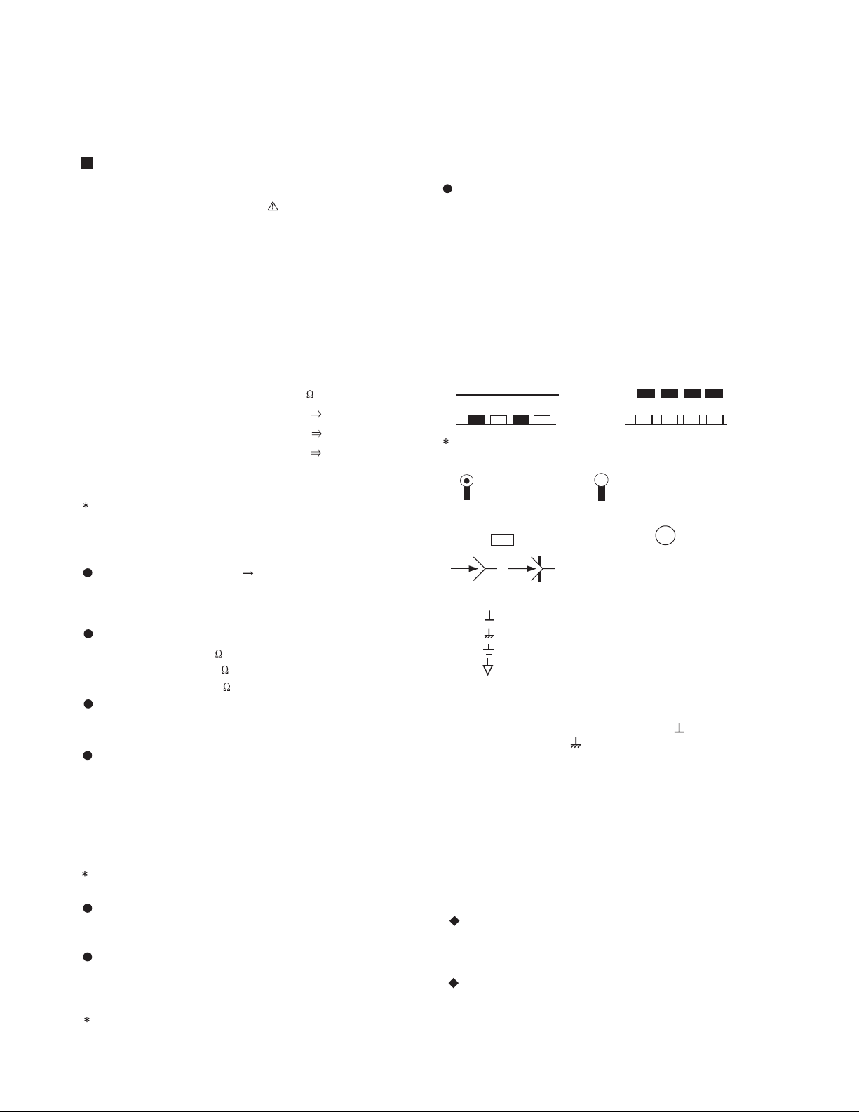
3.INDICATION OF PARTS SYMBOL [EXAMPLE]
In the PW board
: R1209
R209
Type
No indication
MM
PP
MPP
MF
TF
BP
TAN
(3)Coils
No unit
Others
(4)Power Supply
Respective voltage values are indicated
(5)Test point
: Test point
(6)Connecting method
: Ceramic capacitor
: Metalized mylar capacitor
: Polypropylene capacitor
: Metalized polypropylene capacitor
: Metalized film capacitor
: Thin film capacitor
: Bipolar electrolytic capacitor
: Tantalum capacitor
: [µH]
: As specified
: B1
: 9V
: Only test point display
: Connector
: Receptacle
: Wrapping or soldering
: B2 (12V
: 5V
)
4.INDICATIONS ON THE CIRCUIT DIAGRAM
(1)Resistors
Resistance value
No unit :[
K
M
Rated allowable power
No indication : 1/16 [W]
Others : As specified
Type
No indication
OMR
MFR
MPR
UNFR
FR
Composition resistor 1/2 [W] is specified as 1/2S or Comp.
(2)Capacitors
Capacitance value
1 or higher : [pF]
less than 1
Withstand voltage
No indication : DC50[V]
Others : DC withstand voltage [V]
AC indicated
Electrolytic Capacitors
47/50[Example]: Capacitance value [µF]/withstand voltage[V]
]
]
: [k
: [M
]
: Carbon resistor
: Oxide metal film resistor
: Metal film resistor
: Metal plate resistor
: Uninflammable resistor
: Fusible resistor
: [µF]
: AC withstand voltage [V]
(7)Ground symbol
: LIVE side ground
: ISOLATED(NEUTRAL) side ground
: EARTH ground
: DIGITAL ground
5.NOTE FOR REPAIRING SERVICE
This model's power circuit is partly different in the GND. The
difference of the GND is shown by the LIVE : ( ) side GND and the
ISOLATED(NEUTRAL) : ( ) side GND. Therefore, care must be
taken for the following points.
(1)Do not touch the LIVE side GND or the LIVE side GND and the
ISOLATED(NEUTRAL) side GND simultaneously. if the above
caution is not respected, an electric shock may be caused.
Therefore, make sure that the power cord is surely removed from
the receptacle when, for example, the chassis is pulled out.
(2)Do not short between the LIVE side GND and ISOLATED(NEUTRAL
side GND or never measure with a measuring apparatus measure
with a measuring apparatus ( oscilloscope, etc.) the LIVE side GND
and ISOLATED(NEUTRAL) side GND at the same time.
If the above precaution is not respected, a fuse or any parts will be broken.
Since the circuit diagram is a standard one, the circuit and
circuit constants may be subject to change for improvement
without any notice.
NOTE
Due improvement in performance, some part numbers show
in the circuit diagram may not agree with those indicated in
the part list.
When ordering parts, please use the numbers that appear
in the Parts List.
)
No.52166
2-1
Page 2
CONTENTS
SEMICONDUCTOR SHAPES ......................................................................2-2
BLOCK DIAGRAM........................................................................................2-3
CIRCUIT DIAGRAMS....................................................................................2-5
MAIN PWB CIRCUIT DIAGRAM ................................................................................................................ 2-5
CRT SOCKET PWB CIRCUIT DIAGRAM................................................................................................... 2-9
PATTERN DIAGRAMS ...............................................................................2-11
MAIN PWB PATTERN...............................................................................................................................2-11
CRT SOCKET PWB P ATTERN................................................................................................................. 2-13
CHANNEL CHART(US).............................................................................. 2-15
CHANNEL CHART(CA).............................................................................. 2-16
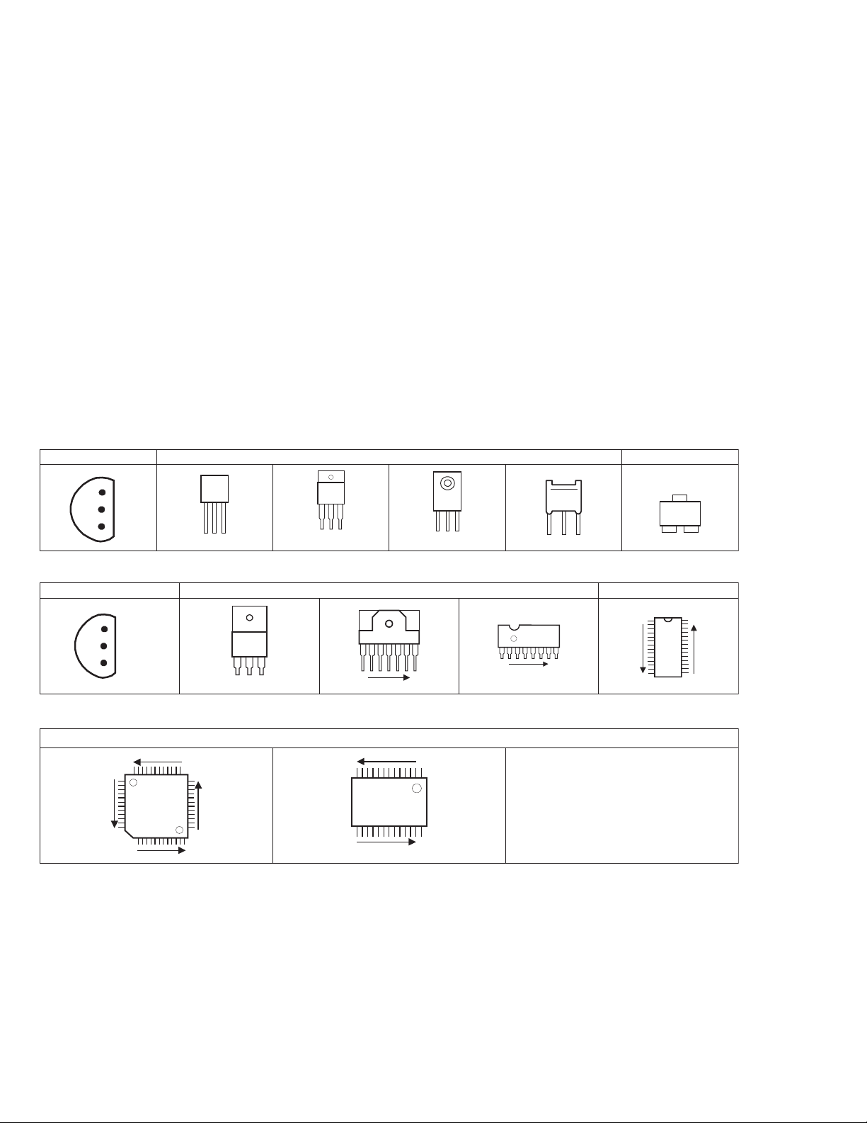
SEMICONDUCTOR SHAPES
TRANSISTOR
BOTTOM VIEW FRONT VIEW TOP VIEW
CHIP TR
E
C
B
ECB
B
(G)E(S)C(D)
ECB
ECB
C
BE
IC
BOTTOM VIEW FRONT VIEW TOP VIEW
OUT
E
IN
IN OUTE
1 N
1 N
CHIP IC
TOP VIEW
N
N
N
1
N
1
N
1
N
2-2
No.52166
Page 3
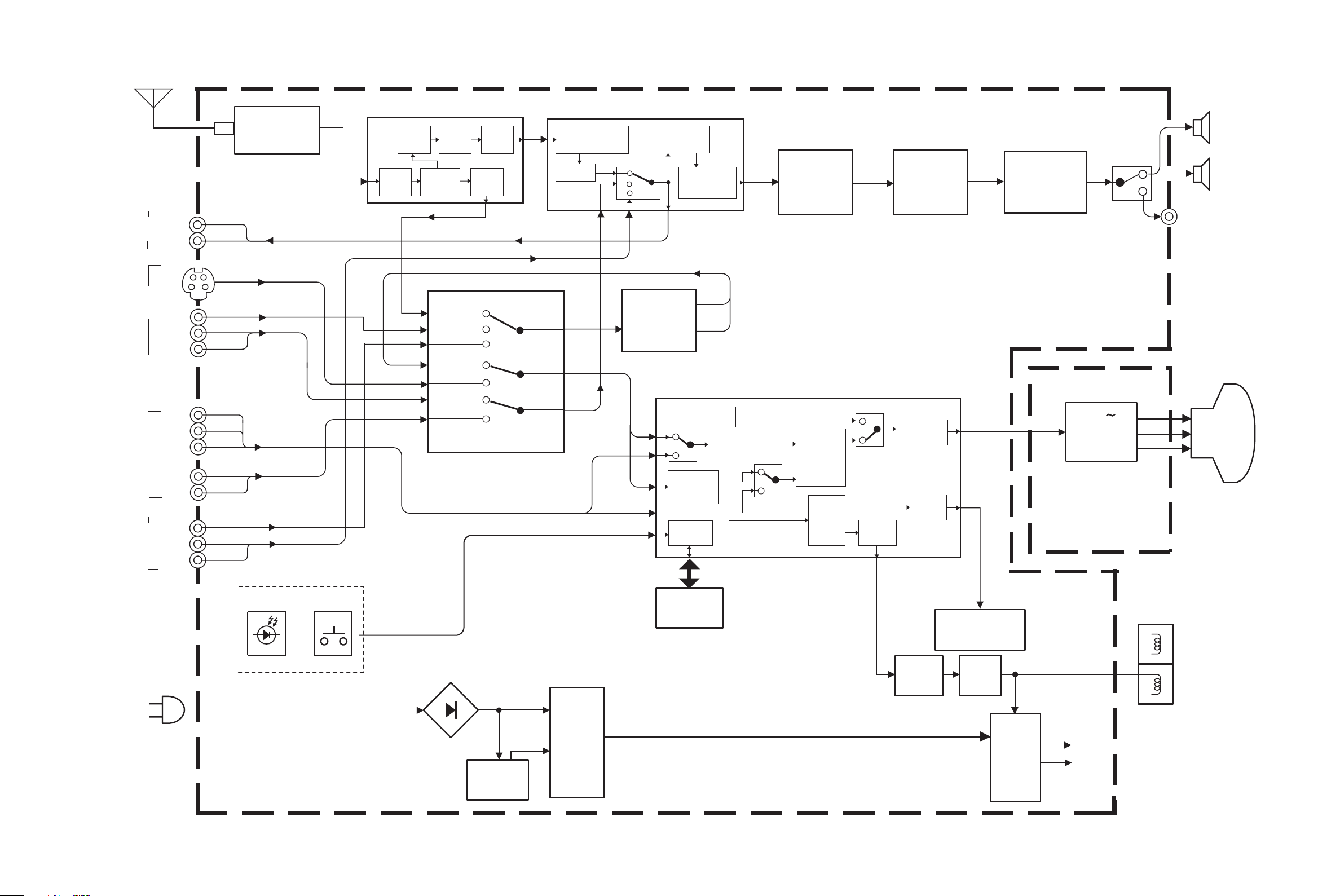
BLOCK DIAGRAM
AUDIO
OUT
Y/C
INPUT 1
VIDEO
AUDIO
COMPONENT
VIDEO
INPUT 2
AUDIO
VIDEO
INPUT 3
AUDIO
L
R
V1
L1
R1
Y
Pb
Pr
L2
R2
V3
L3
R3
Y1/C1
TU001
TUNER
Y/Pb/Pr
IF
IC101
IF
AMP
LIMIT
AMP
IF & DET
FM
DET
VIDEO
DET
AF
AMP
EQ
AMP
VTV
IC651
STEREO
MPX
AUDIO L/R OUT
DEMODULAT
MATRIX
AUDIO L/R
L3/R3
MTS DECODE & AUDIO CONTROL
SURROUND
TONE/VOL
CONTROL
L/R
IC641
A.H.S
L/R
IC601
BBE
L/R
IC602
AUDIO OUT
L/R
L
R
SPEAKER
SPEAKER
HEADPHONE
L
R
MAIN PWB
Y
Y
KEY
IC251
Y/C SEP
Y
C
CHROMA
DEMOD
CPU
C
Y
PROCESS
IC201
OSD
GENERAT.
MICRO COMPUTER
/CLOSED CAPTION DECODER
/VIDEO.SYNC.DEF. PROCESS
RGB
CHROMA
CONTROL
/ MATRIX
SYNC
SEP.
PROCESS
V.
OSC.
H.
OSC.
H
R/G/B
V
Q301
Q321
RGB OUT
CRT SOCKET
PWB
(Within MAIN PWB)
CRT
V1
V3
Y/C
Y1/C1
L1/R1
L2/R2
IC851
V
Y/C
AUDIO L/R
AV SW
Pb/Pr
AC IN
RM SW
T921
D901
SW.
TRANSF.
IC901
POWER REG.
No.52166 No.521662-42-3
IC702
MEMORY
B1
Q501
H.DRIVE
IC421
VERT OUT
Q521
H.OUT
T521
HVT
(V)
(H)
DEF. YOKE
(ITC)
FOCUS
SCREEN
Page 4

CIRCUIT DIAGRAMS
MAIN PWB CIRCUIT DIAGRAM (1/2
)
C648NC649
10/5010/50
N
IC641 C647R647 R648
NJM2701M-X 10/5010K 10K
AHS
C645C643C641 C642 C646
1/5010/504700P .027 100/16
R646R645
47K5.6K1K10K
Q642
*1
C644
X
C663
C665
R657
C664
1/50
1/50
1.5k
10/50
33k
R671
C661C667 R660 R656
R655
0.133/50 5.6K 3.3k
AHSSW
3.3M
IC651
UPC1851BGT
0.1
C670
C672
C673
C674
C671
2.2/50
2.2/50
.0022
.0022
AHSMODE
56K
R659
.022
C669
AHSMODE
SDA0
SCL0
ER3
EL3
R
L
LOT
ROT
R642
R644
Q641
*1
R641
R643
1K
22K
C668
1/50
R661
100
R670 R669
100 100
R662
100
R664
0
R663
0
N
C677
10/16
N
C678
10/16
MAIN PWB ASS'Y (1/2
SFJ-1001A-M2 (AV-20FA44)
SFJ-1002A-M2 (AV-N21A44)
PIN NO. PIN NO. PIN NO.
VOLTAGE (V)VOLTAGE (V)VOLTAGE (V
A_VCC
GND
V-OUT
HD
FBP
ABCL
MAIN_PW
9V
BT
5V
STBVCC
IC101
1 1.7
2 4.5
3 3.8
4 1.3
5 1.4
6 0
7 0
8 0
9 0
10 3.9
11 2. 4
12 4.5
13 2
14 3.4
15 2
16 8.8
17 8.8
18 3.9
19 3.9
20 4.7
21 4.7
22 0
23 3.4
24 1.6
IC201
1 0
2 2.6
3 5
4 0
5 5
6 2.2
7 2
8 0
9 5
10 0
11 0
12 0
13 0.8
14 1.8
15 8.8
16 6.2
17 3.5
18 4.4
19 NC
20 30
21 NC
22 2
23 2.3
24 2
25 3.4
26 2.1
27 NC
28 2.3
29 0
30 2.1
31 5.9
32 NC
33 2.2
34 NC
35 1.6
36 2.6
37 2.8
38 NC
39 2.1
40 2
41 2.3
42 8.7
43 0
44 0
45 0
46 5
47 0.2
48 NC
49 4.6
50 4
51 4.9
52 1.7
53 4.9
54 0
55 4.9
56 NC
IC251
1 4.8
2 1.2
3 3
4 2.2
5 1.7
6 4.8
7 0
8 4.8
9 4.4
10 3.8
11 0
12 0
13 2.4
14 1.8
15 4.8
16 0
17 2.3
18 3
19 1.7
20 2.2
IC601
1 4.3
2 4.3
3 4.3
4 4.3
5 4.3
6 4.3
7 4.3
8 8.6
9 8.6
10 7.4
11 0
12 8.8
13 4.3
FRONT INPUT HEADPHOENE
J007
CEMN072-003
AUDIO OUT
R621
33K
R623
1.8k
GND
R622
33K
R624
1.8k
R626
X
R625
X
C625
D621
*5
C131
.01
AFT
AGC_ADJ
Q001
*4
AGC-M
SDA1
CN00C
QGA2501F1-06
LC687
QQR1199-001
C623
.001
C624
.001
Q622
C626
X
X
R135
SDA0
SCL1
QNN0282-001
C628
1uF
X
1k
Q131
*1
QQLZ014-R39
C104
.01
C105
.01
SCL0
R687
D687
IC751
GP1UM281QK
R758
100
C751
47/25
R757
100
C752
X
REMOCON
C621
1/50
C622
1/50
A_MUTING
F_V
VTV
YOUT
C211
47/25
COUT
C223
0.01
EL2
ER2
D686
D685
*6
*6
C686
C685
10/50
10/50
CMP_Y
Y686
X
CMP_PB
Y685
X
CMP_PR
J004
QNN0348-001
Y856
X
Y854
0
0
Y855
X
QQR0621-002Z
R285
Q283
330
Q282
*2
R286
1k
R295
330
Q292
*2
R296
1k
K255
D807
*6
J001
QNZ0454-001
REAR INPUT
R287
1K
Q293
R297
1K
QSW0619-003Z
*1
*1
S752
S753
QSW0619-003Z
R753R752
1.5k1k
LOT2
ROT2
C615
X
C602
1uF
C601
1uF
C613
X
Q352
R356
R288
0
R298
0
V1
Y1
D801D803
*6*6
C801
10/50
D802
*6
R801
68
C802
10/50
R802
75
C683
10/50
C684
10/50
S755
S754
QSW0619-003Z
QSW0619-003Z
R754
2.7k 5.6k
R602
R604 C609
C606
C604 C610
22K
22K 47/25
.0330.0033 0.01
N
IC601
NJM2150AD
N
C603
C605
R601
R603
.00330.033
22K
22K
BBE
*2
R354
330
D352C352
12k
*647/25
Q233
QQL29BJ-560Z
EL1
ER1
J003
QNN0349-002
D683
*6
D684
*6
S751
QSW0847-001
CRT SOCKET PWB
R751
1k
LOT2
ROT2
AHSSW
R652
15k
C657
R653
2.2/50
4.7k
C656
4.7/50
R651
C659 C658
R654C662
1k
.47/50 .047
68k3.3/50
C660
0.1
C675
N
C655
1/50
N
R667 R668
100 100 100 100
0.1
EXTR
EXTL
C654
0.1
R665 R666
C653
47/25
C652
C651C666 R658
.01
100/101/50 15k
C676
1/50
IC704
AN78L05-T
C702 C703
10/50 10/50
IC851
TA1218AN
VIDEO/AUDIO
SELECT
BBE_SW
R778
10k
IC702
AT24C04-20FA44
A_MUTING
R703 R707D705
10k 10k*5
IC703
S-80840CNY-T
R851 R852 R853
100 100 100
C807
.01
C710
X
R257
2.2k
L
C862
10/50
EL1
ER1
V1
C701
.001
IC201
CEXJIM00009
R717
4.7K
R715
100
R821
R706
120k
4.7k
C815
0.01
R251
3.3k
Q251
*2
R254
180
R252
R253
10k
1k
R
COUT
YOUT
C861C860
47/25 .01
C851 C852 C854 C855 R772 R774
C853
.01 .01 .01 .01 10k 10k
10/50
R854
R855
100 100
15K
VTV
Y1
)
REMOCON
R721R701
1k1K
R714
82k
AFT
R255
1.5k
C857
10/50
R856
SDA1
SDA0
SCL0
SCL1
LED
AGC_ADJ
R716
X
D702
X
R718
22k
R705
4.7k
R708
R709
100
100
R702
1K
KEY1
C713
C709
22p
0.01
Y253
BW
C253
47p
L251
4.7
X
Y293
C252
C254
100p
180p
F_V
100
100
100
R860
R859
R858
X
X
C863
CMP_Y2
ER2
C864
C1
EL2
C716
10/50
R704
4.7k
100
R731
C708
22p
X701
QAX0717-001Z
QQR0582-001Z
Q252
*2
R256
1.5k
SDA0
15k
R771
X
C865
R768
R769
D367
6.8k
1k
*5
D366
*5
Q701
*1
D365
*5
R770
10k
R734R733
4.7k4.7k
.01
22k
47/25
C711
C712
R729
100
R740
100
R732
C705
R739 R501
.01
2.7k
C704
47/25
AGC-M
K701
K702
QQR0582-001Z
K251
QQR0582-001Z
C261
.01
C262
47/25
C263
.01
C264
.01
C265
.47/50
C266
.01
Y252
BW
C267
.01
Y251
0
K253
QQR0582-001Z
C269
.01
SCL0
SCL0
R775C856C858
R776R777R861C859
100100100.01
10k.01.01
10k
R773
R857
10k
R720
1.0
100X100
47/25
.01
R366
R363
C361
C362
X
R360
0
R362
C504
2.2/50
4.7k
R504
X
.01
C503
3.9K
680
R502
R503
C502C501
.01 47/25
FBP
HD
YC SEP.
IC251
TC90A49P
C268
47/25
C270
47/25
R261
100
R262
100
Q851
*1
KEY1
CN00T
QJB003-064826
D370
MTZJ5.1B-T2
D369
1K
MTZJ5.12B-T2
D368
MTZJ5.1B-T2
R318
R227
R201
R241
R319
100k
22k
X
100
47/25
R364
R365
X
C243
R361
R401
1k
C401
C505
.47
.47
V-OUT
C402
1000p
R863
47k
4.7K
.01
C244
C202
R505
150k
R862
100k
D353
*5
.1
0.01
C354
C303
.0015
2.2/50
1/50
C203
C247
R359
10k
C241
C221
0.01
10/50
C237
X
R837
R836
100
100
CMP_Y
K254
QQR0582-001Z
R264
820
C273
.01
A_MUTING
R838
X
R506 R507
470 560
CMP_PR
R263
100
C689
33/50
EXTL
EXTR
.01
C506
C507
X
47/25
.01
Q291
Y281
Y292
XX
Q681
*2
D681
*6
D682
*6
*2
Q683
C835
X
C836 C837
X
R835
R834
100
CMP_PB
C278
.01
C277
.01
C276
.01
47/25
C275
180p
C274
.01
C272
LED
C222
.1
D501
MTZJ3.3A-T2
R282
2.2k
Q281
*1
R292
2.2k
*1
C681
10/50
C682
10/50
Q751
*3
R756
1.2k
D751
LG22440
POWER
C282
X
L281
R283
820
QQL29BJ-150Z
C283
33p
Y295
X
C292
X
Y294
R293
R294
470
X
L291
QQL29BJ-220Z
C293
47p
C1
C803
1/50
R684R683
R803
22K22K
75
AUDIO
OUTPUT
J002
Q682
*2
QNN0348-001
R681
220
R691
82K
R682
R692
220
22K
Q684
R686R685
22K22K
*2
S756
QSW0619-003Z
R755
C608
R605
R607
R609
C607
10/50
10K
R608
X
R606
X
BBE_SW
R215
5.6K
Q211
*2
R212
2.7K
R217
R216
1K
5.6K
R232
3.9K
R231
1.8K
*2
C233
68p
R233
3.3K
R234
L232
1.5K
Q232
*2
R235
1k
CMP_Y2
Y852
X
C834
D834
*6
10/50
C831
.1
R831 D831
75 *6
C832
.1
D832
*6
R832
75
C833
.1
D833
R833
*6
75
220
*6
ER3
Q621
X
R133
820
R117
27k
L101
2SC5083/L-P/-T
C102
J006
CEMN065-002
QNN0281-002
D688
*6
LC688
QQR1199-001
EL3
IC602 LA4485
C627
1uF
D623
*5
C632
47/25
R627
10K
R134
680
Q101
R104
R105
R767
R688
220
C688C687
10/5010/50
C629
100/16
C633
47/25
D622
*5
Q625
UN2212-X
L131
QQL29BJ-220Z
CF131
QAX0639-001Z
IC101
M52342FP
IF/
DET.
R111
390k
R115
100
R113
100
R112
330k
R103
QRE121J-101Y
18
R102
1.8k
2782.01
QQR0582-001Z
SDA0
SCL0
R765
R766
470
470
470
J005
CEMN065-001
QNN0281-003
LC801
QQR1199-001
Q623
*1
R631
10K
C101
R008
K001
R764
470
R804
75
C804
10/50
D804
*6
R805
100
1000/25
R628
3.3k
C634
R632
33K
R633
R132
220
C120
C113 C114 C124
.01 .01 .01
R101
5.6k
.01
QAX0349-001
C004
470/6.3
R005
H602CEXJIM00008
R629
22k
C630
R630
22K
Q624
X
X
X
R131
1k
C119
680p68.47/50
R116
CF001
C003
47/35
Y101
0
Y102
X
C002
.01
0
R006
22k
J008
QNS0155-001
R637
R636
270
270
Y603
X
Y604
X
C636
Q626
*2
T111
QQR0907-001
SF101
QAX0723-001
QAU0274-001
1000/25
R635
3.3k
D625
X
R634
D624
3.3k
X
C637
1000/25
R638
3.3
C163
47p
CH
QAX0642-001Z
C164
47p
CH
R164
1k
L161
QQL29BJ-220Z
.01
47/25
C107
C106
33k
22K
R171
R163
C116
R161
.22
3.3k
C161
10/50
K101
QQR0582-001Z
TU001
C631
.47/50
C635
X
C005
.01
R004
C006
220
X
R003
220
C007
X
C001
4.7/50
CN00S
QGA2501C5-04Z
A_VCC
GND
V-OUT
HD
FBP
GNDGND
A_VCC
C167
.01
R165
R167
22K
1K
CF161
Q161
*2
BUFFER
R166 R168
10K 100
C165
.01
R169
560
C166
.01
C162
10/50
14 4.3
15 4.3
16 4.3
17 4.3
18 4.3
19 4.3
20 4.3
IC602
1 0
2 13.5
3 1.1
4 0
5 12.4
6 7
7 13.5
8 7
9 12.3
10 0
11 1. 1
12 0
13 0
IC651
1 4.5
2 3.9
3 0
4 0
5 4.3
6 4.3
7 4.3
8 4.3
9 4.3
10 4.3
11 4. 2
12 4.3
13 4.3
14 4.3
15 4.3
16 4.3
17 4.3
18 4.3
19 4.3
20 4.3
21 4
22 8.6
23 4.3
24 4.3
25 4.3
26 4.3
27 4.3
28 4.3
29 5.8
30 1.4
31 3.1
32 4.2
33 4
34 4.9
35 4.3
36 1.1
37 4.9
38 3.8
39 4
40 4.7
41 4.1
42 0
IC702
1 0
2 0
3 0
4 0
5 5
6 5
7 0
8 5
IC703
1 5
2 5
3 0
IC704
1 9
2 0
3 5
IC851
1 3.7
2 0
3 6.3
4 3.5
5 5
6 5
7 5
8 5
9 5
10 5
11 5
12 5
13 6
14 1.7
15 5
16 5
17 5
18 1.7
19 0
20 0
21 0
22 0
23 0
24 4.1
25 4.6
26 1
27 0
28 5
29 5
30 5
31 5
32 5
33 8.7
34 3.6
35 3.8
36 3.6
37 3.8
38 4.2
39 3.7
40 3.7
41 8
42 4.2
TU001
AGC 1.8
NC
ADRS 4.2
SCL 4.4
SDA 4.6
NC
5V 4.9
NC
BT 33.1
NC
IF 0
Q001
E 0
C 3.8
B 0
Q101
E 0.9
C 8.6
B 1.6
Q131
E 1.8
C 0
B 1.1
Q161
E 1.9
C 5.6
B 2.5
Q211
E 3.6
C 8.6
B 4.1
Q232
E 0
C 1.1
B 0
Q233
E 3.2
C 8.6
B 3.9
Q251
E 2.9
C 4.8
B 3.6
Q252
E 2.3
C 4.8
B 2
Q281
E 2.8
C 0
B 2.2
Q282
E 2.2
C 4.2
B 2.8
Q283
E 4.8
C 2.7
B 4.2
Q291
E 2.9
C 0
B 2.4
Q292
E 2.3
C 4.2
B 3
Q293
E 4.8
C 2.9
B 4.2
Q352
E 6.5
C 8.6
B 7.1
Q602
E 0
C 13.5
B 0.1
Q681
E 0
C 0
B 0.1
Q682
E 0
C 0
B 0.1
Q683
E 0
C 0
B 0.1
Q684
E 0
C 0
B 0.1
Q701
E 1.4
C 1.4
B 0.6
Q751
E 5
C 4.9
B 0
Q851
E 8.6
C 1.7
B 8.5
)
IC201-13
5
IC201-14
60
IC201-18
2
IC201-26
0.5
IC201-28
0.8
IC201-39
4.8
IC201-40
3.2
No.52166 No.521662-5 2-6
IC201-41
6
IC251-4
1
IC251-17
0.5
IC251-20
1
IC851-10
1
IC851-34
0.5
IC851-36
1
TU101-18
2
Page 5

MAIN PWB CIRCUIT DIAGRAM (2/2
)
QMPD200-200-JC
QQW002-001
QGZ5004C1-02
PIN NO.
VOLTAGE (V
IC421
1 4.2
2 27.2
3 2
4 0
5 16.1
6 28.3
7 4.2
IC901
1 139
2 0
3 0
4 32.1
5 1.5
IC921
1 11.4
2 9
3 0
IC922
1 7.3
2 0
3 4.8
Q501
E 0
C 66.5
B 0.2
Q521
E 0
C 135
B 0
Q921
E 0
C 0.6
B 1.2
Q922
E 0
C 9
B 0
Q923
E 9
C 0
B 9
Q924
E 133.7
C 0
B 133.3
CN0PW
L01
CNDEG
)
FC901
CEMG002-001Z
IC901
STR-G5624A/F8
QMF51N1-5R0-J5
ERZV10V621CS
QRT029J-R22
K903
QQR0582-001Z
HS009
LC31678-001A
5.0A
R904
C910
470p
F901
CH
QFZ9075-104
VA901
QCZ9054-102
TH901
QAD0129-3R0
CEKP007-002
QRF074K-R47
K904
QQR0582-001Z
QQR0582-001Z
QQR0582-001Z
R908
QRK126J-681X
D907
MA700A-T2
D904
*8
C909
NCB31HK-122K
D908
MTZJ15C-T2
C901
C904
R901
R905
QRT029J-R22
K901
K902
4.7K
47/50
LF901
QQR0527-003
D901
GSIB460-S1
QEZ0376-477
QEZ0561-477
C908
QCZ0340-222
QFP32GJ-103Z
R902
47K
R903
47K
R907
1/2W
C907
C902
QFZ9075-104
C905
QCZ9054-102
C903
C911
1/2W
D905
SARS01-T2
1/2W
D902
*8
D903
*8
D906
X
QQT0355-001
QRZ9041-275
RELAY
RY901
QSK0085-001
T921
QQS0158-001
QQS0203-001
R910
680K
1/2W
R911
1W
47
R906
2.2
1/2W
T901
C991
R991
* DIFFERENCE LIST
2SA949/Y/Z1-T 2SA1208/ST/Z1-T
Q924
C991
QCZ9074-103 QCZ9073-332
QCZ9074-103 IM-BW
C992
IC421 AN5522
D921
*9
D924
*9
R922
1k
R923
47K
C929
QCZ0340-102
R924
QRX01GJ-1R0
C931
QCB32HK-102Z
D928
C921
470/25
R934
27K
D931
*5
Q922
2SC2785/JH/-T
D926
RU3AM-LFC4
L921
QQL26AK-470Z
C923
QEZ0203-107
QQL26AK-470Z
C925
470/16
C927
470/25
L922
R933
C946
X
12K
R935
33K
CN0B1
CH41169-R03Y
R929
22K
1/2W
R930
47K
1/2W
C924
47/160
C940
0.01
C926
100/16
R932
C935
47/16
Q923
*1
12K
R939
10K
47/35
R938
10K
1/2W
R937
X
Q924
C933
IC921
AN7809F
*
1/2W
R936
10K
1/2W
R926
1.2
C932
100/6.3
R928
2.7K
D929
MTZJ7.5A-T2
18
R941 2WOMR
9V
C941
100/16
D922
*9
D923
*9
D925
*5
C922 R921
OPT BW
Q921
2SD1383K/AB/-X
C992
*
*
K921
QQR0582-001Z
K924
X
C930
QCB32HK-102Z
D927
K922
R925
QRX01GJ-1R0
K923
RU3YX-LFC4
RU3YX-LFC4
QQR0582-001Z
QQR0582-001Z
MAIN PWB ASS'Y (2/2
D933
1N4002G-T2
MTZJ33B-T2
2W
R927
2W
1.2
1/2W
R931
C943
0.01
D932
B1
X
D930
STBVCC
R942
1/2W
C942
100/16
5.6
BT
MAIN_PW
R943 1/2W
82
IC922 AN7805F
9V
5V
C944
100/16
)
5V
C945
0.01
GND
A_VCCA_VCC
GND
ABCL
HD
FBP
CN00D
X
Q501
2SC4212/Z1/
R508
100
R509
270
Y501
0
V-OUT
VP
QRL039J-272
QRL039J-332
QRE121J-103Y
C508
QCB32HK-151Z
MA4068N/Z1/-T2
R535
R511
R512
R510
C509
QCB32HK-331Z
R403
10k
R404
X
C510
2.2/250
R405
10k
D526
R534
CE42034-002
XX
T501
R406
15K
R533
NRZ0032-3241X
H002
LC30381-001A
R521
QRE121J-220Y
C405
10/50
C403
10/16
R402
N
10K
CNHHS
CH41169-R03Y
R532
X
R531
NRZ0032-7151
Q521
2SD2634-YD
C521
QCZ0325-821
C408
C404
1000P
D525
*7
C522
QFZ0198-562
C529
47/35
L521
OPT
Y521 IM-BW
Y522 IM-BW
C523
QFZ0197-534
R529
QRK126J-4R7X
C530
QFLC2AJ-103Z
R530
QRX029J-1R5
C528
1000/35
C524
OPT
OPT
R522
D402
MTZJ75-T2
C407
100/35
QRE121J-472Y
C531
X
D524
RGP10J-5025-T3
R523
QRL039J-152
QRE121J-184Y
HS004
LC31696-001A
C406
1000p
K401
QQR0582-001Z
C413
X
D401
*9
D523
1SR35-400A-T2
R528
R525
R413
R414 R411
X
10K 12k
R412
15K
R415
X
C525
QEZ0203-107
R541
QRE121J-683Y
R524
C409
QFLC2AK-104Z
C410
QFLC2AK-104Z
C412
2.2/50
R410
X
RH1S-T3
R527
L522
opt
T521
QQH0128-001
C526
.082
MY
1SR35-400A-T2
QRE121J-681Y
QRK129J-150
D522
D521
SFJ-1001A-M2 (AV-20FA44)
R407
C411
2200/35
R409
QRX01GJ-1R0
C532
X
R526
SFJ-1002A-M2SFJ-1001A-M2
CN0HV
R408
QRE121J-681Y
R416
QRE121J-102Y
S401
QSL4A13-C02
C527
10/250
V
CN0HV
CN10HV
DEF YOKE(V)
CN00U
HB
HEATER
DEF YOKE(H)
QJB003-044024
CRT SOCKET
PWB
CRT SOCKET
PWB
SFJ-1002A-M2 (AV-N21A44)
IC421-5
65
IC421-3,6
38
Q501-B
1
No.52166 No.521662-82-7
200
Q501-C
Q521-B
2
1300
Q521-C
32
T521-2
120
T521-3
310
T521-7
T521-8
70
Page 6

CRT SOCKET PWB CIRCUIT DIAGRAM
2SC4075/DE/YA11
R302
12K
2WOMR
Q301
R303
1.5k1/2W
SK351
CRT SOCKET
CRT SOCKET PWB ASS'Y
SFJ-3001A-M2
MAIN PWB
(1/2)
MAIN PWB
(2/2)
CN00T
QGA2501C5-06Z
CN00U
QGA2501C5-04Z
CN00D
Y001
OPEN
L341
QQL29BJ-390Z
Y341
X
C342
X
C101
10/50
R143
680
R142
120K
R136 R134
39K 3.3K
R139
560
2SA933AS/QR/-T
Q109
2SC1740S/QR/-T
R144
OPEN
C127
OPEN
Q103
R331
D331
D334
*5
OPEN
*5
R334
3.9K
K102
1K
R335
OPEN
Q152
1.5K
220/10
R332
D332
Q151
OPEN
R154
OPEN
R153
OPEN
R305
270
R312
12K
2WOMR
2SC4075/DE/YA11
12K
R325
C302
330p5%
R313
1.5k
C312
270p5%
R315
270
R323
1.5k
1/2W
Q321
2SC4075/DE/YA11
C322
270p5%
270
R306
100
1/2W
R316
100
R326
Y342
BW
TP-E
100
Y343
BW
QCZ0121-102
C343
.001
3KV
C301
R301
150
R311
150
C311
C341
R321
R333
1K
*5
D333
1K
*5
C321
X
R304
3.3k
Q311
X
R314
3.3k
R322
2WOMR
150
X
R324
3.3k
Q301-C
C331
220/10
*10
R152
OPEN
R151
OPEN
Q331
C152
OPEN
C151
OPEN
C108
OPEN
R115
C109
OPEN
R116
47
47
R122
4.7k2W
R121
OPEN
C114
QCB32HK-472Z
C111
OPEN
C115
QCB32HK-472Z
C110
OPEN
.0047
C113
10/160
C117
10/160
R123
4.7K
R126
220k
R127
220k
R128
4.7K
R125
R129
22
22
R124
180
Q107
2SA1964/DE/
K104
2SC5248/DE/
Q108
R130
180
R131
470
R145
R146
C118
100/6.3
22
D105
RH1S-T3
R132
390
QRL029J-391
K105
D106
RH1S-T3
22
C119
100/10
C120
330/10
C121
150p
QCS32HJ-151Z
150
CN00V
CEXJIM00012
PICTURE TUBE
VM COIL
MAIN PWB
(2/2)
Q311-C
Q321-C
120160
PIN NO.
VOLTAGE (V
Q103
E 2.8
C 8.8
B 3.4
Q107
E 115
C 56
B 113
Q108
E 2.7
C 56
B 3
Q109
E 1.5
C 3.4
B 2.1
Q301
E 1.7
C 158.4
B 2.2
Q311
E 1.8
C 155.3
B 2.2
Q321
E 1.8
C 156.7
B 2.2
Q331
E 8.2
C 0.1
B 8.8
)
No.52166 No.521662-9 2-10
Page 7

PATTERN DIAGRAMS
MAIN PWB PATTERN
K902
C903
R901
D904
R908
D908
C904
LF901
IC901
W901
C909
K901
C901
VA901
CL003
R907
C910
R991
D901
CL002
HS009
C991
C905
C902
F901
S751
D903
D902
W902
W903
D907
K904
R905
R904
W905
W904
R932 R933
Q922
R935
W918
CL002B
C911
C992
Q923
C907
K903
R910
C935
R906
C908
D906
R934
D930
D929
D905
R911
R937
RY901
W911
R931
C932
TH901
W912
T901
R921
C922
D931
Q924
R929
D751
R928
Q921
D923
D924
W909
R756
R903
R902
T921
R926
R923
R922
D925
W908
Y638
IC751
W920
K921
D922
D933
R927
C924
W930
R638
C751
R941
W929
W814
C752
K923
K924
C923
R930
W917
C929
W616
R757
R925
K922
L921
D921
IC921
W907
C941
C943
W632
W633
W925
R758
W910
W922
W678
Q751
R924
W928
W927
W926
W923
D927 D928
D926
C933
C921
C678
W679
C925
L922
R297
R298
Q293
R293
C926
C940
W677
W919
C927
C930
C859
C677
C946
Q292
C292
R231
C703
Q682
R254
R296
Y295
R294 R295
R232
R216
W627
R717
W713
C702
R720
C931
Q681
R685
Q683
R686
R252
Y294
C233
R217
R706
R627
R682
R692
R684
Q684
Q251
C293
Q291
Y281
Q233
R233
R212
IC704
C689
R257
R251
C274
Y251
W813
W717
W718
W734
S752
J002
R691
R683
R292
C252
R255
C254
W251
R256
Y253
W811
Q211
R702
W711
C701
W716
W723
R863
R862
R852
W681
W806
C253
Y293
C266
Q232
D705
W942
W941
W733
Y855
R681
D803
D807
W810
R215
IC703
W715
W719
W732
W710
W709
W721
D684
C684
R253
K254
R701
R721
C807
W722
Q851
W815
C211
R261
R235
L232
W714
R751
R803
J001
W812
L251
Q252
R262
IC201
IC702
R752
C803
R861
R778
C862
R263
C270
C269
W257
R715
C704
C711
C710
S753
R802
C272
W253
R234
W623
R801
W805
R851
IC851
C860
C273
W204
C705
R703
R707
R709
W624
C858
C223
W258
C276
W203
R714
C815
R821
X701
C716
R718
R716
R853
C851
R264
C267
W205
C713
R705
R708
D802
C275
R704
R731
R753
D683
W801
R854
C852
W808
K701
C709
C708
R733
R732
R740
W720
W662
S754
C683
W802
C802
W836
R857
C854
C861
L291
Y292
C268
W259
K702
R739
R734
W729 R729
W728
D702
R768
R769
W661
J004
C801
C855
K253
W707
C502
R503
Q701
R770
W361
Y854
D686
D801
Y852
R855
C864 C865
C857
W809
C265
Y252
W501
C503
C712
C686
C863
W807
C264
IC251
R504
R366
C362
C361
W362
R754
Y685
C685
C856
C263
K251
K255
W252
C501
D366
D365
D367
S755
R833
Y686
C831
R771
C262
W706
R365
Y856
D685
R772
C278
C277
R364
R831
R773
L281
C261
R163
R167
R166
R165
W254
C402
C504
R401
R318
D834
W643
R774
R286
C283
W271
C282
Q281
Q161
D369
D368
D370
C834
W131
W114
R776
R777
W132
R287
R283
R282
C167
C165
R168
W708
C401
W965
R755
D831
R856
R775
R285
Q282
R288
C166
R169
R502
C243
J003
R832
C833
D833
C832
R858
W115
C853
Q283
C163
R171
C164
CF161
R834
W832
C202
R360
S756
D832
R859
R860
W161
L161
R835
R836
W831
R501
C303
R362
R363
R006
R005
C007
C006
C002
C005
R008
C162
R164
W833
R839
C247
R361
W687
C161
C507
D501
R505
C244
W689
R161
W111
W272
R359
C505
R241
C203
W688
CF001
C116
W291
W206
D353
C835
C836
R319
TU001
R003
Y101
C101
Y102
SF101
IC101
T111
W281
C506
R201
C221
C837
C354
R227
R004
R132
L131
Q131
W113
R354
D352
R356
C241
C001
C003
R102
C104
W002
C113
C114
W651
W652
W207
C682
D687
C004
R936
R101
R135
W834
C352
C681
R104
Q352
LC688
R689
R767
D932
R103
R115
R131
R116
W954
R837
R838
C687
R766
W003
R105
Q101
L101
Q001
W953
W952
C237
C222
C666
D682
R687
C102
W102
CF131
W963
W951
R659
LC687
R939
C105
R113
W106
C120
C119
R506
C665
D681
R938
C124
W682
R507
C667
D688
C688
J006 J007
K001
W105
C107
R133
R134
K101
W680
C663
C664
R668
R667
C679
R765
C106
R112
R111
R117
C131
W701
W702
W103
W703
W704
W705
W712
W961
C662
C680
R690
R764
W964
R660
R666
R663
R664
C659
LC801
R688
C528
S401
W654
C668
R665
R805
J005
C531
R530
W653
R661
D524
R528
W401
W655
R652
IC651
R662
W403
D401
W404
C530
D525
R653
C657
C660
R670
W506
W505
R409
R404 R405
R403
W409
W353
W656
R657
R658
C658
C655
C669
R669
D804
R804
C804
R402
C404
IC421
C405
R406
HS004
R942
C661
R671
R655
R656
C656
R651
J008
R410
R413
C406
C403
W507
W405
R654
C654
C412
C942
R943
C653
C674
R415
IC922
C649
W641
C651
C652
C671
R416
R414
R412
R411
W402
C413
C407
W406
W642
C675
C670
R636
C408
W407
C945
C648
C676
W640
T521
C411
K401
D402
R601
R602
C944
W646
C646
C673
R637
W644
W645
IC601
IC641
C672
Y604
Y603
W636
R407
R408
R603
R604
C602
C641
C409
C645
C605
C606
C613
C603
C615
R641
C642
C643
R645
R642
C601
C604
R643
Q641
Y521
Y522
W621
C522
C410
R647
W626
R646
W625
C527
C532
D522
R526
C521
H002
C523
L521
R522
C524
Q501
R508 R509
R606
R608
Y501
C621
C626
R607
R605
C610
C647
C609
R648
C608
C630
Q642
R644
C631
C644
C607
R609
C636
R635
C632
C633
R628
D623
R625
Q623
C508
C509
C622
C629
R634
C634
C625
R523
T501
Q622
R622
W607
D622
D523
R525
Q521
R521
D625
C637
R631
L522
W503
R621
R626
C624
R632
Q625
R510
R624
R633
R527
W509
R529
R524
W502
R623
C628
R630
HS602
CL005
D621
C529
C525
C623
R629
R534
R531
D526
R541
W504
C510
C627
D624
W622
R535
W508
D521
C526
R512
W510
IC602
W630
C635
R533
R532
R511
FRONT
Q621
Q624
Q626
CL005B
No.52166 No.521662-122-11
Page 8

CRT SOCKET PWB PATTERN
TOP
R314
R316
C341
W353
D333
W351
R311
D331
R321
R335
C321
R324
R325
C322
R326
C311 C312
R315
D334
W354
D332
R331
SCREEN
43
3
C
C331
R334
Q331
W352
R323
Q321
R313
Y342
Y341
Q311
TP-E
R322
R301
C301
R305
C302
R306
R304
C151
R129
R131
W001
D105
Q108
D106
R125
C118
K104
R145
R126 R127
R128
C120
R123
C115
C109
Q109
C127
Q107
C114
R154
Q151
R116
R115
C108
R148
R134
R153
C111
C110
R139
R144
Q152
C152
Q103
R151
K102
R152
R143
Q301
R302
R
31
2
R303
L341
Y343
C342
SK351
U
W101
C101
R147
R122
Y001
C113
C117
C121
W002
R132
V
R130
R136
R142
R124
K105
R146
C119
No.52166 No.521662-13 2-14
Page 9

CHANNEL CHART (US
)
MODE
TV REAL DISP.
CATV
BAND
VL
VH
MID
SUPER
HYPER
ULTRA
CHANNEL
A
B
C
D
E
F
G
H
I
J
K
L
M
N
O
P
Q
R
S
T
U
V
W
W+1
W+2
W+3
W+4
W+5
W+6
W+7
W+8
W+9
W+10
W+11
W+12
W+13
W+14
W+15
W+16
W+17
W+18
W+19
W+20
W+21
W+22
W+23
W+24
W+25
W+26
W+27
W+28
W+29
W+30
W+31
W+32
W+33
W+34
02
03
04
05
06
07
08
09
10
11
12
13
14
15
16
17
18
19
20
21
22
23
24
25
26
27
28
29
30
31
32
33
34
35
36
37
38
39
40
41
42
43
44
45
46
47
48
49
50
51
52
53
54
55
56
57
58
59
60
61
62
63
64
65
66
67
68
69
70
TUNER
BAND
I
II
I
II
IV
MODE
TV REAL DISP.
CATV
NOTE:
TO RECEIVE THE SUBSCRIPTION OR PREMIUM
PROGRAMMING FROM CERTAIN
CABLE COMPANIES.
SPECIAL ADAPTERS MAY BE REQUIRED.
BAND
ULTRA
SUB
MID
UHF
TOTAL 180CH
VHF
UHF
CHANNEL
W+35
W+36
W+37
W+38
W+39
W+40
W+41
W+42
W+43
W+44
W+45
W+46
W+47
W+48
W+49
W+50
W+51
W+52
W+53
W+54
W+55
W+56
W+57
W+58
W+59
W+60
W+61
W+62
W+63
W+64
W+65
W+66
W+67
W+68
W+69
W+70
W+71
W+72
W+73
W+74
W+75
W+76
W+77
W+78
W+79
W+80
W+81
W+82
W+83
W+84
A-8
A-4
A-3
A-2
A-1
124CH
56CH
71
72
73
74
75
76
77
78
79
80
81
82
83
84
85
86
87
88
89
90
91
92
93
94
100
101
102
103
104
105
106
107
108
109
110
111
112
113
114
115
116
117
118
119
120
121
122
123
124
125
01
96
97
98
99
14
69
TUNER
BAND
IV
I
IV
No.52166
2-15
Page 10

CHANNEL CHART (CA
)
MODE
TV REAL DISP.
CATV
BAND
VL
VH
MID
SUPER
HYPER
ULTRA
CHANNEL
02
03
04
05
06
07
08
09
10
11
12
13
A
B
C
D
E
F
G
H
I
J
K
L
M
N
O
P
Q
R
S
T
U
V
W
W+1
W+2
W+3
W+4
W+5
W+6
W+7
W+8
W+9
W+10
W+11
W+12
W+13
W+14
W+15
W+16
W+17
W+18
W+19
W+20
W+21
W+22
W+23
W+24
W+25
W+26
W+27
W+28
W+29
W+30
W+31
W+32
W+33
W+34
14
15
16
17
18
19
20
21
22
23
24
25
26
27
28
29
30
31
32
33
34
35
36
37
38
39
40
41
42
43
44
45
46
47
48
49
50
51
52
53
54
55
56
57
58
59
60
61
62
63
64
65
66
67
68
69
70
TUNER
BAND
I
II
III
IV
MODE
TV REAL DISP.
CATV
NOTE:
TO RECEIVE THE SUBSCRIPTION OR PREMIUM
PROGRAMMING FROM CERTAIN
CABLE COMPANIES.
SPECIAL ADAPTERS MAY BE REQUIRED.
BAND
ULTRA
SUB
MID
UHF
TOTAL 180CH
VHF
UHF
CHANNEL
W+35
W+36
W+37
W+38
W+39
W+40
W+41
W+42
W+43
W+44
W+45
W+46
W+47
W+48
W+49
W+50
W+51
W+52
W+53
W+54
W+55
W+56
W+57
W+58
W+59
W+60
W+61
W+62
W+63
W+64
W+65
W+66
W+67
W+68
W+69
W+70
W+71
W+72
W+73
W+74
W+75
W+76
W+77
W+78
W+79
W+80
W+81
W+82
W+83
W+84
A-8
A-4
A-3
A-2
A-1
124CH
56CH
71
72
73
74
75
76
77
78
79
80
81
82
83
84
85
86
87
88
89
90
91
92
93
94
100
101
102
103
104
105
106
107
108
109
110
111
112
113
114
115
116
117
118
119
120
121
122
123
124
125
01
96
97
98
99
14
69
TUNER
BAND
IV
I
II
IV
2-16
No.52166
 Loading...