

Page 1
SERVICE MANUAL
PLASMA WIDE TELEVISION
AV42PD20ES
BASIC CHASSIS
CONTENTS
AV42PD20ES
MF
! SPECIFICATIONS ・・・・・・・・・・・・・・・・・・・・・・・・・・・・・・・・
! SAFETY PRECAUT IONS ・・・・・・・・・・・・・・・・・・・・・・・・・・・・・・・・
!
WARNI NG
!
FEATURES ・・・・・・・・・・・・・・・・・・・・・・・・・・・・・・・・
! FUNCTIONS・・・・・・・・・・・・・・・・・・・・・・・・・・・・・・・・
!
TECHN ICAL INFORMAT ION
! INSTALLATIONS・・・・・・・・・・・・・・・・・・・・・・・・・・・・・・・・
!
SPECIFIC SERVICE INSTRUCTIONS
!
SERVICE ADJUSTMENTS ・・・・・・・・・・・・・・・・・・・・・・・・・・・・・・・・
! TROUBLESHOOTING・・・・・・・・・・・・・・・・・・・・・・・・・・・・・・・・
!
PARTS LIST
★
OPERATING INSTRUCTIONS
★
STAND ARD CIRCUIT DIAGRAM
1
・・・・・・・・・・・・・・・・・・・・・・・・・・・・・・・・
・・・・・・・・・・・・・・・・・・・・・・・・・・・・・・・・・・・・・・・・・・・・・・・・・・・・・・・・・・・・・・・・
・・・・・・・・・・・・・・・・・・・・・・・・・・・・・・・・・・・・・・・・・・・・・・・・・・・・・・・・・・・・・・・・
・・・・・・・・・・・・・・・・・・・・・・・・・・・・・・・・・・・・・・・・・・・・・・・・・・・・・・・・・・・・・
・・・・・・・・・・・・・・・・・・・・・・・・・・・・・・・・・・・・・・・・・・・・・・・・・・・・・・・・・・・・・・・・
・・・・・・・・・・・・・・・・・・・・・・・・・・・・・・・・・・・・・・・・・・・・・・・・・・・・・・・
・・・・・・・・・・・・・・・・・・・・・・・・・・・・・・・・・・・・・・・・・・・・・・・・・・・・・・・・・・・・・・・・
・・・・・・・・・・・・・・・・・・・・・・・・・・・・・・・・・・・
・・・・・・・・・・・・・・・・・・・・・・・・・・・・・・・・・・・・・・・・・・・・・・・・・・・・・・・・・・・・・・・・
・・・・・・・・・・・・・・・・・・・・・・・・・・・・・・・・・・・・・・・・・・・・・・・・・・・・・・・・・・・・・・・・
・・・・・・・・・・・・・・・・・・・・・・・・・・・・・・・・・・・・・・・・・・・・・・・・・・・・・・・・・・・・・・・・
・・・・・・・・・・・・・・・・・・・・・・・・・・・・・・・・・・・・・・・・・・・・・・・・・・・・・・・・・・・・・・・・
・・・・・・・・・・・・・・・・・・・・・・・・・・・・・・・・・・・・・・・・・・・・・・・・・・・・・・・・・・・・・・・・
・・・・・・・・・・・・・・・・・・・・・・・・・・・・・・・・
・・・・・・・・・・・・・・・・・・・・・・・・・・・・・・・・・・・・・・・・・・・・・・・・・・・・
・・・・・・・・・・・・・・・・・・・・・・・・・・・・・・・・・・・・・・・・・・・・・・・・・・・・・・・・・・・・・・・・
・・・・・・・・・・・・・・・・・・・・・・・・・・・・・・・・・・・・・・・・・・・・・・・・・・・・・・・・・・・・・
・・・・・・・・・・・・・・・・・・・・・・・・・・・・・・・・・・・・・・・・・・・・・・・・・・・・・・・・・・・・・・・・
・・・・・・・・・・・・・・・・・・・・・・・・・・・・・・・・
・・・・・・・・・・・・・・・・・・・・・・・・・・・・・・・・・・・・・・・・・・・・
・・・・・・・・・・・・・・・・・・・・・・・・・・・・・・・・・・・・・・・・・・・・・・・・・・・・・・・・・・・・・・・・
・・・・・・・・・・・・・・・・・・・・・・・・・・・・・・・・・・・・・・・・・・・・・・・・・・・・・
・・・・・・・・・・・・・・・・・・・・・・・・・・・・・・・・・・・・・・・・・・・・・・・・・・・・・・・・・・・・・・・・
・・・・・・・・・・・・・・・・・・・・・・・・・・・・・・・・・・・・・・・・・・・・・・・・・・・・・・・・・
・・・・・・・・・・・・・・・・・・・・・・・・・・・・・・・・・・・・・・・・・・・・・・・・・・・・・・・・・・・・・・・・
・・・・・・・・・・・・・・・・・・・・・・・・・・・・・・・・
・・・・・・・・・・・・・・・・・・・・・・・・・・・・・・・・・・・・・・・・・・・・・・・・・・・・・・・・・・・・・・・・
・・・・・・・・・・・・・・・・・・・・・・・・・・・・・・・・・・・・・・・・・・・・・・・・・・・・・・・・・・・・・・・・
・・・・・・・・・・・・・・・・・・・・・・・・・・・・・・・・
・・・・・・・・・・・・・・・・・・・・・・・・・・・・・・・・・・・・・・・・・・・・・・・・
・・・・・・・・・・・・・・・・・・・・・・・・・・・・・・・・・・・・・・・・・・・・・・・・・・・・・・・・・・・・・・・・
COPYRIGHT © 2002 VICTOR COMPANY OF JAPAN, LTD.
・・・・・・・・・・・・・・・・・・・・・・・・・・・・・ 2
・・・・・・・・・・・・・・・・・・・・・・・・・・・・・・・・・・・・・・・・・・・・・・・・・・・・・・・・・・
・・・・・・・・・・・・・・・・・・・・・・・・・・・・・・・・・・
・・・・・・・・・・・・・・・・・・・・・・・・・・・・・・・・・・・・・・・・・・・・・・・・・・・・・・・・・・・・・・・・
・・・・・・・・・・・・・・・・・・・・・・・・・・・・・・・・・・
・・・・・・・・・・・・・・・・・・・・・・・・・・・・・・・・・・・・・・・・・・・・・・・・・・・・・・・・・・・・・・・・
・・・・・・・・・・・・・・・・・・・・・・・・・・・・・ 11
・・・・・・・・・・・・・・・・・・・・・・・・・・・・・・・・・・・・・・・・・・・・・・・・・・・・・・・・・・
・・・・・・・・・・・・・・・・・・・・・・・・・ 36
・・・・・・・・・・・・・・・・・・・・・・・・・・・・・・・・・・・・・・・・・・・・・・・・・・
・・・・・・・・・・・・・・・・・・・・・・・・・・・・・・・・・・・・
・・・・・・・・・・・・・・・・・・・・・・・・・・・・・・・・・・・・・・・・・・・・・・・・・・・・・・・・・・・・・・・・
・・・・・・・・・・・・・・・・・・・・・・・ 4
・・・・・・・・・・・・・・・・・・・・・・・・・・・・・・・・・・・・・・・・・・・・・・
・・ ・
・・ ・・・ ・
・・ 6
・・・・
・・ 7
・・・・
・・・・・・・・・・・・・・・・・・・・
・・・・・・・・・・・・・・・・・・・・・・・・・・・・・・・・・・・・・・・・
・・・・・・・・・・・・
・・・・・・・・・・・・・・・・・・・・・・・・
・・・・・・・・・・・・・・・・・・・・・ 21
・・・・・・・・・・・・・・・・・・・・・・・・・・・・・・・・・・・・・・・・・・
・・・・・・・・・・・・・・・・
・・・・・・・・・・・・・・・・・・・・・・・・・・・・・・・・
12
37
2- 1
5
9
No.519 55
May 2002
Page 2
A
V42PD20ES
SPECIFICATIONS
Item CONT ENTS
Dimensions ( W××××H××××D ) 10 4.8 cm ×11 4.0c m× 35 .8c m
Mass 58 .0 kg
TV RF System CCIR B/G, I, D/K, L ,L’
Colour Syst em PA L / SE CAM & NT SC 3.5 8 / N TSC 4. 43 ( NTSC p la y b ack on l y)
Sound System A2 ( B/G , D/K), NICAM (B/G , I, D/ K, L)
Teletext System Fastext(United Kingdom system), TOP(German syst em), WST(World standard system)
Rec eiving
Frequency
French CATV 116MHz~17 2MH z / 2 20 MH z~4 69M H z
Intermediate
Frequency
Colour Sub
Carrier
Power Input AC 2 20V~2 40V , 5 0H z
Power Consumption 380W ,2A ( Max. ) / 2 80W (A vg.) / 5 .5 w (St and by)
PDP S ize Vis ible ar ea 10 5.7 cm, [ Meas ured diag on ally]
Speake r
Au dio Output Rated
An ten na Input
Input / Output
Terminals
Au dio ou tp u t RCA pi n typ e, V ari ab le au dio L/R o utput ar e avail a ble
PC Input
Headphone Jack
Remote Control Unit RM-C59 (AAA/R03 dry ce ll b atte ry×2)
Design and specifications are subject to change without notice.
VHF 47 MHz ~ 470MHz
UHF 470MHz~86 2MHz
VIF Carrier 38.9 MHz( B/G , D/K, I, L) / 3 3.95MHz (L’)
SIF Carrier 33.4 MHz( 5. 5MHz : B/ G) / 32 .9 MHz( 6.0MHz : I)
32.4 MHz(6.5 MHz : D/ K, L) / 40.45M Hz(6.5 MHz : L’)
PAL 4.43MHz
SE CAM 4. 4062 5MHz / 4 .25 MHz
NT S C 3.58MHz / 4.43 MHz ( pl a y bac k)
8cm round×2 , 16 cm roun d×1 ( su b wo ofer) / 4Ω
5W + 5W ( L+R) / 20 W(su b woof er)
75Ωun ba l anc ed, C oaxial
EX T-1
EX T-2
EX T-3 21-p i n E uro c onnecto r ( SC A RT s ocket), Vi de o, Aud i o L/R , RGB signa l i npu t a r e a va ilable
EX T-4 RCA pin type, S-Video, Video and Audio L/R signal input are available
21 -p i n E uro c onnec to r (SC A RT s ocket) , Vi de o, Aud io L/R , RGB signa l i npu t a r e a va i lable
TV br oad c ast out put (Vide o and Au dio L/R) are ava ilab l e
21 -p i n E uro c onnec to r (SC A RT s ocket) , S-V i de o, Video , A udio L/ R, RGB s ign al inpu t a re a vailable
AV select or ( TV LIN K ) func ti on is avai l able
D-Sub 15 pin ×1 / si gnal (R, G, B / H&V SYNC)
St ereo min i jac k (φ3.5mm )
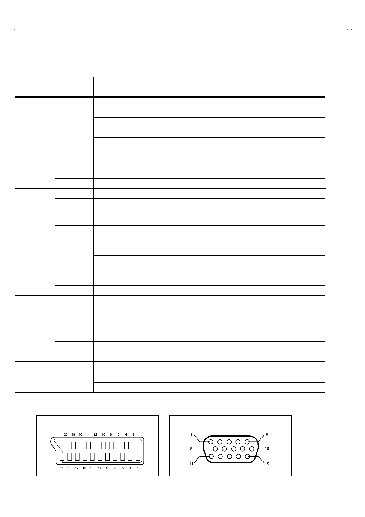
[21pin Euro connector pin assignment] [PC IN connector]
(15pin D-Sub connect or pin assignm ent)
2
No. 51955
Page 3
A
V42PD20E
S
]
]
640×480
■■■■21-PIN EURO CONNECTOR (SCART socket) : EXT-1 / EXT-2 / EXT-3
(P-P= Peak to Peak, S-W= Sync tip to white peak, B-W= Blanking to white peak)
Pin Signal Designation Matching Value EXT-1 EXT-2 EXT-3
1 AUDIO R o utput 50 0mV (r ms) , Low i m pe dance
2 AUDIO R i n put 50 0m V(r ms) High i mp ed ance
3 AUDIO L output 500mV(rms), Low impedance
4 AUDIO GN D ○○○
5 GND (B) ○○○
6 AUDIO L input 500mV(rms), High impedance
7B input 700mV
FUNCTION SW
8
(SLOW SW)
9 GND (G)
10 SCL1 NC
11 G in put 70 0m V
12 SDA1 NC ○ NC
13 GND (R) ○○○
14 GND (YS)
15 R / C input
16 Ys i n put L ow : 0V - 0. 4V, H i gh : 1 V - 3V , 75 Ω○ ○ NC
17 GND(VIDEO output) ○○○
18 GND(VIDEO input) ○○○
19 VID EO outpu t
20 VIDEO / Y inp ut 1V
21 COMMON GN D ○○○
(B-W )
, 75Ω○○NC
Low : 0V-3V,
High : 8V-12V ,H i gh imped anc e
(B-W )
, 75Ω○○NC
R : 700mV
C : 300mV
1V
(B-W)
, 75Ω
(P-P)
75Ω
(P-P )
(Neg ati ve goi n g s ync), 75 Ω
(P-P )
(Neg ati ve goi n g s ync), 75
Ω
○
(TV OUT)
○○○
○
(TV OUT)
○○○
○○○
○○○
○○
○
(only R)
○
(TV)
○
(only V IDEO in pu t)
○
(LINE OUT)
○
(LINE OUT)
○
○
○
(LINE OUT) NC
○○
NC
NC
NC
NC
○
(only C )
■■■■15-PIN D-SUB CONNECTOR (PC IN connector)
Ea ch t ype si gna l o f co mp ut er
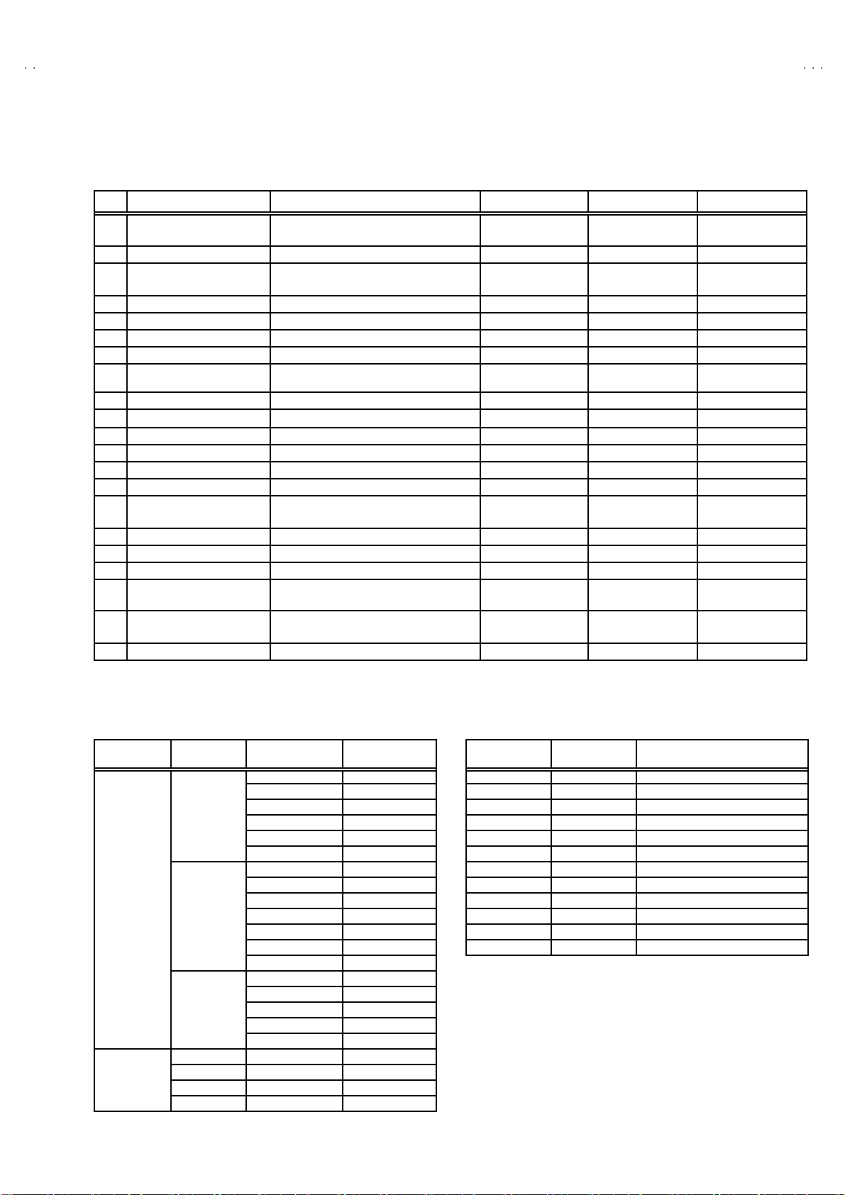
Model Resolution
IBM P C/AT
compatible (VGA) 37.9 72.8
80 0×600 35.2 56.3
(SV GA) 37 .9 60 .3
10 24 ×768 48.4 60.0
(XGA) 56.5 70.1
Apple 640×480 35.0 66.7
Macintosh 832×624 49.7 74.6
10 24 ×768 60.2 74.9
11 52 ×870 68.7 75.1
Ho r iz ont a l
Frequency [kHz
31 .5 59 .9
37 .5 75 .0
43 .3 85 .0
51 .1 10 0.4
61 .3 12 0.4
48 .1 72 .2
46 .9 75 .0
53 .7 85 .1
63 .0 99 .8
75 .7 12 0.0
60 .0 75 .0
68 .7 85 .0
80 .5 10 0.6
Ve rtical
Frequency [Hz
PC IN connector [ 15pin D-sub pin assignment ]
Pin No. Signal Name Details
1 RED Red vi deo signal
2 GR EE N Gr ee n vid eo s igna l
3 BLUE Blue video signal
4 ― N ot c onnect ed
5-8 GN D Sign al e arth
9 ― N ot c onnect ed
10 GND Sign al earth
11 ― N ot c onnect ed
12 ― ――――――
13 HSYNC Horiz ont al syn chron ous signal
14 VSYNC Vertical synchronous signal
15 ― ――――――
No. 51955
3
Page 4
A
V42PD20ES
SAFETY PRECAUTIONS
<<<<専用
専用
専用専用
PDP
対応>
対応>
対応>対応>
02 -0 3- 19,
中嶋
中嶋
中嶋中嶋
1. The d esign of th is prod uct con ta ins sp ecial har d ware, ma ny
circuit s and components specially for saf ety purposes. For
con tinu ed pr ot ecti on , n o chan g es sh ould b e ma de to the o rig i nal
d esign un less a uth or ized in writi n g by th e manu fac t urer .
Replacem ent p arts m ust b e i d entic al to thos e u sed in th e or i gi n al
ci rcu its. S er v i ce sho ul d b e p er for m ed by qu alif ied p ers on nel
on ly.
2. Alte r ation s of t he des ig n or circui try of t he prod uc ts sh ould not be
made. Any design alterations or additions will void the
manu fac t urer 's warra nt y and will f urth er r el i eve t he ma nufac tu rer
of r esp onsib ili ty for per s o na l injury or pr operty d am ag e res ul t ing
th erefr om.
3. Man y electr i c al an d m ec h ani ca l p ar ts i n th e pr od uc ts ha v e
special safety-related chara cteristics. T hese characteristics are
oft en no t e vi den t f r om v i sua l insp ecti on nor ca n t he pro tect io n
aff orde d by th em nece ssarily be ob tain ed b y u s in g r ep l ac em en t
com po nents rated for hig he r vo l tag e, watt age, etc . R ep lac em en t
p arts whic h have th ese sp ecial s afet y ch ar act erist ics ar e
ide ntified in the parts list of Ser vic e manua l. El ectric al
components having such features are ide ntified by shading
on the sche mat ic s and b y (!!!! ) on the parts list in Service
manual. The us e of a sub sti tu te r ep lac em en t which do es n ot
h ave th e sam e s af ety c h ar ac t erist ics as t he reco mmen ded
replac ement par t sh ow n i n th e parts list of Ser v i ce man ual m ay
cause shock, fire, or other hazards.
4. Don't shor t between the LIVE s ide ground and ISOLATED
(NE UTRAL) side ground or EARTH side ground when
repairing.
Some model's power circuit is partly different in the GND. The
diff erenc e of th e G ND i s sho wn b y th e LIVE : (") side GN D, the
ISO LATE D(N EU TR AL) : ( #) side G ND and EARTH : ($) side
GND. D o n't sh ort b et ween th e LIV E s i d e GND an d
ISO LATE D(N EU TR AL) si de GND or EAR TH side GN D an d
n ever mea sure w it h a mea sur i ng a ppa r atus ( osci l lo scop e etc.)
th e LI VE sid e GN D an d IS OLA TED(NE UTRAL ) s ide G ND or
EARTH sid e GND at the s ame time.
If above not e will not be kept, a fuse or any parts will be broken.
5. If any repair has been made to the chassis, it is recommended
th at t he PDP volt age setti ng sh oul d be check ed or adj ust ed .
6. When se r vic e is r equ ire d, ob serve th e or i gina l lea d dr ess. E x tr a
prec aut i on sh ou ld b e given t o assur e cor r ect l ea d dress in th e
high vol tag e circui t a rea. W her e a s hor t c i r cuit h as occ u rr e d,
th ose co mpon ent s tha t indica te evide nce of ove r hea ting should
b e r e place d. A lways u s e th e manuf act ur er 's rep lacem ent
components.
7. Isolation Check
(Safety for Electrical Shock Hazard)
Af ter r e- ass embl in g th e p r odu ct, always per f orm an i solat io n
ch eck on the expo s ed me tal p ar ts of t he cabin et ( a nte nn a
ter m i na ls, vid eo /au dio i npu t and outpu t t ermi n al s, C on trol kn obs,
metal cabin et, sc r ew he ad s, ea rph one j ack, con tr ol s haf ts, etc.)
to be su re th e p r odu ct is s af e t o o pe rate with ou t d an ger of
elect rical shoc k.
(1) Dielectric Strength Test
The iso lation be tw een the AC pr im a ry ci rcu it an d al l me tal p arts
exp osed t o the us er, p ar ticular ly an y e xpos ed met al p art having a
retu rn p ath to t he c hass is sho uld withs tan d a vol t age of 150 0V
AC (r.m. s.) for a period of one sec ond.
This meth od of test r equi res a test equipment n ot g enerall y fou nd
in t he serv ic e trad e.
(2) Leakage Current Check
Plug th e AC l in e c ord d irect ly into the A C ou tlet ( d o not use a lin e
isol ati o n transf orm er du r ing this ch eck.). U sin g a " Lea kag e
Current T este r", me as ur e th e l ea k ag e cu rr e nt f rom eac h ex p os ed
metal p ar t of the cabine t, p art icu lar ly any e x pos ed me tal p art
h aving a re turn pa th to the ch assis , to a kn own go od ea rt h
grou nd (w a ter pip e, e tc.). An y l eaka ge c ur r en t must n ot e xceed
3.5mA AC (r.m.s.).
Howev e r, in trop ic al ar ea , th is mu st no t ex ce ed 0.2 mA AC
(r.m.s.).
""""
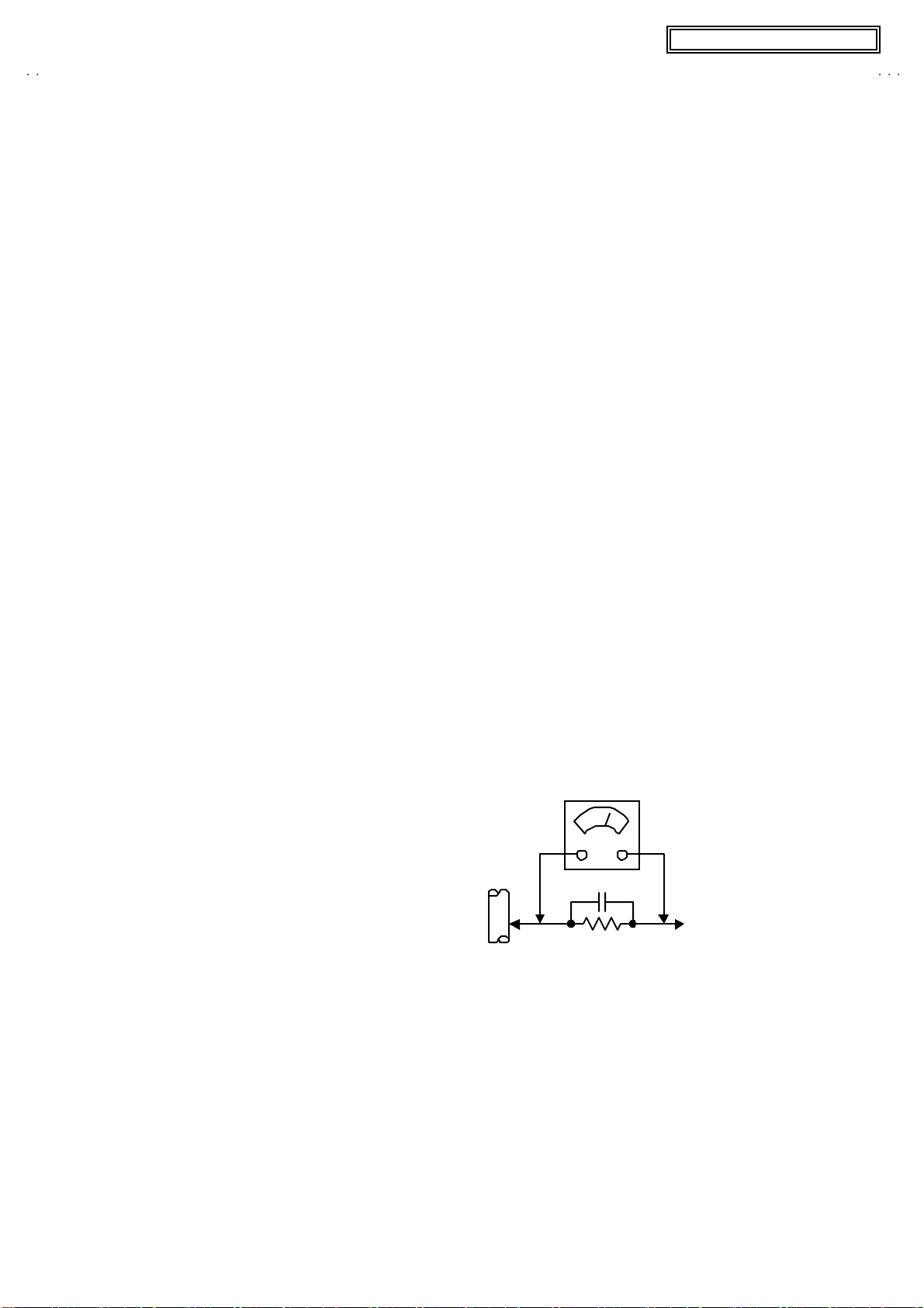
Alte rn at e Che ck M et hod
Plug th e AC l in e c ord d irect ly into the A C ou tlet ( d o not use a lin e
isol ati o n tran sfor m er dur i ng this c he c k.). Use an AC vo lt meter
having 1000
Connect a 1 500 Ω 10W resistor paralleled by a 0.15µF AC-type
cap acitor b etwe en an e xpos ed me tal part a nd a kn own g ood
ea rt h gr o und ( water p ipe, etc.) . M eas ur e t he AC volta ge acr oss
the resistor with the AC voltmeter. Move the resistor connection
to e ach expos ed met al pa rt, par ti c u l arly an y exp ose d m eta l par t
h aving a re turn pa th to th e ch assis, and me asure th e AC vo ltag e
acr os s t he res is tor. Now, re v er se the plug in the AC o utlet an d
repe at each m eas u re m ent . A ny volta ge measu red m us t not
exce ed 0 .7 5V A C (r .m. s.) . Thi s corresp onds to 3.5 mA AC
(r.m.s.).
Howeve r, in tropica l area, this must n ot exce ed 0 .3V AC ( r .m.s.).
This corresponds to 0.2mA AC (r.m.s.).
GOOD EARTH GROUND
Ω /
V or more sensitivit y in the following mann er.
AC VOLT MET ER
(HAVING 1000 Ω /V,
OR MOR E SENSIT IVITY)
0.15μF AC -T YPE
PLACE THIS PROBE
1500 Ω 10W
ON E A C H EX PO SE D
ME T AL PA RT
4
No.51955
Page 5

A
V42PD20E
S
SAFETY PRECAUTIONS
1. The des i gn of thi s pr odu ct c ont ai ns spe cial har d ware and many
circuit s and components specially for saf ety purposes. For
con tinu ed pr ot ecti on , n o chan g es sh ould b e ma de to the o rig i nal
d esign un less a uth or ized in writi n g by th e manu fac t urer .
Replacem ent p arts m ust b e i d entic al to thos e u sed in th e or i gi n al
ci rcu its. Se r v ic e sh ou ld be pe rf or me d b y qua li fi e d per s o nn el
on ly.
2. Alte r ation s of the desi g n or circ uitr y of th e pr od uct s ho ul d not b e
made. Any design alterations or additions will void the
manu fac t urer 's warra nt y and will f urth er r el i eve t he ma nufac tu rer
of r esp onsib ili ty for per s o na l injury or pr operty d am ag e res ul t ing
th erefr om.
3. Man y electr ical a nd me c ha ni cal p ar ts i n the pr od uc t h ave spe cial
saf ety- r el at ed ch ar act er ist i cs. Thes e ch aracter istics a re oft en not
evi d ent fr om visu al insp ectio n no r c an th e pr otect ion af for ded by
th em n ec ess ar y b e o bta in ed by using r e plac em ent c ompon en ts
4. The l ea ds in th e p r odu c ts ar e r ou ted an d d ress ed w it h t ies,
[UK MODEL]
rated for wattage, etc. Replacement parts which have these
sp ecial saf et y char acte ristics ar e id enti fie d in t he P art s List of
Se rvi c e Ma nu al. E lectr ical c ompon en ts h aving such feat ur es ar e
identified by shading on the schematics and by (!) on th e Pa rts
List i n th e Ser vice M an ual. Th e us e of a sub sti tu te r ep lac em en t
whic h d oe s n ot hav e t he sa me s af et y ch aracte ris ti c s as th e
reco mmen ded rep l acemen t p art s hown in th e P arts Li s t of
Se rvi c e Ma nu al m ay c ause sh ock, f ire, or o th er haz ards.
cl am ps, tu bing ’s , b arrie rs a nd t he lik e t o be s epa ra ted from live
p arts, h ig h t empe ra ture parts, movi ng parts an d / or sh ar p ed ge s
for t he preven tion of e lec tr i c sh ock and fire h azard. W hen
ser v ice i s r e qu ir ed , the or i gi n al l e ad r outi n g and dre s s sh ould b e
ob served , and it sh oul d b e c o nfirmed t hat th ey h av e b ee n
retu rn ed to no rmal, aft er r e- asse mblin g.
WARNING
1. The e quip me nt has b een d esign ed a nd m an ufact ured t o mee t
inte rn at iona l saf ety st and ards.
2. It i s th e l e ga l re spon s ibility of the rep aire r t o ensu re th at t hes e
saf ety st an dar ds are ma inta in ed.
3. Rep ai rs mu s t be mad e in accor d anc e with the relevan t saf ety
standards.
4. It is esse ntial th at s afet y cri ti ca l c ompon en ts ar e r epl a ced by
ap pr ove d p ar ts.
5. If mains voltage selector is provided, check setting for local
voltage.
No. 51955
5
Page 6
A
V42PD20ES
FEATURES
"
New c hassi s d esign ena bl e us e of an interac tive on screen
control.
"
The TELETEXT SYSTEM h as a built-in FASTEXT (UK system),
TOP (Germ an syst em) and W ST (world standard syst em)
system.
"
Pure FLAT PANEL reproduce fine textured.
" Be caus e th is TV un i t cor r esp on ds t o mul tipl e x br oa dca s t, u ser s
can enjoy music programs and sporting events with live realism.
" In ad diti on , BI LINGUAL pr o gram s can b e h eard in th ei r or i g in al
language.
" Built-in E CO (ECONOMY, ECOLOGY) sen sor MODE.
In acco rd ance with the br ig ht ness in a room, th e brigh tn ess
an d/ or con tr as t of th e pict ure c an be ad jus te d autom at ic al l y to
make the op ti mu m pi ctu re which is eas y on the e ye.
TV EXT-1 EXT-3
"
Users can make VCR dubbing of picture and sound by controlling
th e AV se lecto r t o s elect a n opt ion al s our ce at the E XT -2 ou tpu t
sh own i n figu re.
EXT-4
EXT-2
6
No.51955
Page 7
A
S
FUNCTIONS
FRON T TERMINAL
1 52 3 4
■■■■
FUNCT ION NAM E
1PC IN CONNECTOR (15pin D-sub connec tor)
2HEADPHONE JACK (MINI JACK)
3EXIT-4 TERMINAL
V42PD20E
4VO LUM E ( ) BUTTON
Press this button to display the volume level indicator.
Press the ⑤ up/d ow n ( ∨/∧) b utt ons to cha nge v o l um e w hi le
the volume level indicator is dis played.
5∨/∧
(UP/DOWN ) BUTTONS
Yo u can use th is b utto n as th e ∨/∧ bu tto ns of the PR
ch annel. P re s sing the ④ volume button makes this button
function as the volume - /+ butto ns.
LEFT SIDE TERMINAL
1
2
3
■■■■FUNCT ION NAM E
1
MAIN POWER SW
2
AC INLET
3
AERIAL SOCKET
4
AUDIO OUT (L, R) TERMINAL
5EXT-1(IN/OUT) TERMINAL
6EXT-2(IN/OUT) TERMINAL
7EXT-3(IN) TERMINAL
4
5
7
6
No. 51955
7
Page 8
A
V42PD20ES
i
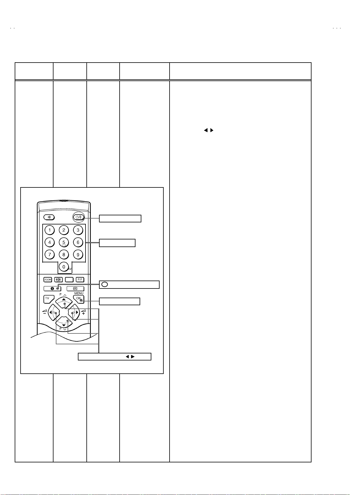
REMOTE CONTROL UNIT
1
2
3
4
5
6
7
15
16
17
18
23
24
■■■■FUNCT ION NAME
1
MUTI N G Key ( )
2
NUMBER (ten) Key
8
9
10
11
12
13
14
19
20
21
22
25
26
3 ZOO M Key
4
HYPER SOUND Key
5
INFORMATION Key ( )
6 TV Ke y
7
VOLUME -/+ Key
8
STAND-BY Key ( POWER)
9
PIP Key
A
CO LO UR K ey
B TEXT Key ( )
C
MENU / OK Key
D
PR C HAN NE L UP/ DOW N (∧/∨) Key
E FU NC TION ( / & ▲/▼) Key
F
MODE Key (F. T/L) : LIST⇔FLOF /TO P
G HO LD Key ( )
H
SUB PAG E Key ( )
I
STORE Key ( )
J SIZE Key ( )
K
REVERSAL Key ( )
L
INDEX Key ( )
M
DISPLAY CANCEL Key ( )
N
TV / TEXT / DVD Key
?
i
O CHANGE Key ( )
P
FREEZE Key
Q
SUB-PAGE (∧/∨) Key
8
No. 51955
Page 9
A
S
TECHNICAL INFORMATION
y
y
y
y
(
)
)
)
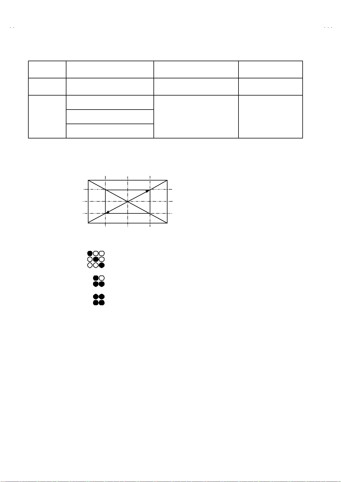
PDP (PLASMA DISPLAY PANEL) DESCRIPTION
! CAUTION
Alth ou gh a PD P i s ma de w i th high ly ad va nc ed p r ecisi on , th is do es n ot nec es sarily m ean a ll o f th e cel l s op er at e cor r ect ly. T he PDP
inevit ably i nc ludes cell th at do no t li gh t or ligh t co ns ta ntly.
If t he sp ecificat ions (PD P p er form an ce) ar e uncle ar at t he t ime of s hip me nt, an adeq uate d escr ip ti on can not be con veyed to t he customer.
In eve nt of i n quiries f rom c usto me rs re ga rd ing PD P p erfor m an ce, chec k th e f ollo w in g s pecifi cat i ons i n or d er to of fer a suita bl e reply.
!
CELL ARR ANGEMENT
The PDP is c ons tru cted of f r ont a nd rear glas s substrat es pr ovid ed with re spec tive di scha rge elec trod es. Be tween th ese , ne on f or
disch ar gi ng an d x eno n f or g ener ating ul tr aviolet r a ys are enclos ed.
On e p ict ur e elem en t (pixel ) i s com po sed of Red, Green an d Bl ue (R GB) cell s. Th e c ell pi tc h is 0.36 mm h or iz ontal (1.08 m m per p ixel) by
1.08mm vertical.
As s hown in Fig.1 , t he cel l s are ar r ang ed fo r each R/G /B c olour. A p ixel consists of each cell of R/G/B / colo ur.
The size of a c el l is 0. 36mm h ori zont al l y an d 1 .08m m v ert i cally.
Direction
Horizontal(H
V42PD20E
Ve rt ic al(V
1ST pixel
2nd pixel
767th pixel
line
768th pixel
line
line
line
1st pixel
arra
2nd pixel
arra
R G B R G B
RGBRGB
G BRG B
R
GBRGB
R
H 1.08mm
Pit ch of pixe l
Fig. 1 PIXEL (CELL) ARRANGEMENT
On e pixel
(1dot)
R cell
G cel l
B ce ll
1023th pixel
arra
1024th pixel
arra
R GBRG B
RGB RGB
G BRG B
R
GBRGB
R
H 0.36mm
Pit ch of cel l
V 1. 08 mm
Pit ch of p ixe l
Pitch of cell
!
PIXEL FAULT
The re ar e two p ixel f aults - b rig ht fault an d d ark f ault - tha t are respe ctivel y d efin ed as f ollows.
(1) BRIGHT FAULT
In this pi xel fault, a c ell tha t sh ould no t li gh t orig inally i s light in g or fl ash i ng on and o ff.
For check ing thi s pi xel f ault, inpu t A LL BL AC K SC R EE N an d fin d o ut the c ell th at is lig hti n g or f lashin g on and of f.
(2) DARK FAULT
In thi s pixel faul t, a cell that sh ould light or i gin al l y is not ligh ti ng or not fl as hing o n and of f or lighti n g with the bright nes s twic e as b ri gh te r
as originally ligh ting.
For check ing th is pi xel f au lt, in put 100% of eac h RG B c olour an d f ind out t he cell t hat is not ligh ting or n ot fl ash in g on an d off or lighting
wit h the br i ght ness as bright er as orig inally l i gh ting.
No. 51955
9
Page 10
A
V42PD20ES
(3) PIXEL FAULT S PECIFICATION
Screen display Criteria for number of faulted cell
Criteria for number of
consecutive faulted cell
Bright faultAll black screen
Red level 100% on entire screen
Gr ee n l ev el 10 0% on en tir e scr eenDark fault
Blue l eve l 10 0% o n ent ire scr een
(Note) A-zone : Center portion
(area enc losed by 1/4 verti call y f rom t he top a nd bot tom a nd 1/ 4 horiz ont all y fr om th e ri gh t and left s id es.)
B-zone : Other area
B zone
A zone
52.9cm
(Note) The c on s ecu tiv e p ixe l f ault t hat are di ag onal l y or in tensi v ely g enera ted s h al l be int erp r ete d a s f ollo ws :
A zone: 2 or less than 2 in each colour
B zone: 3 or less than 3 in each colour
A zone: 3 or less than 3 in each colour
B zone: 8 or less than 8 in each colour
(1/4H)(1/4H)
(1/4V )
(1/4V )
2 or Les s th an 2
con secut ivel y
2 or Les s th an 2
con secut ivel y
→→→→ cons ecut ive 3
→→→→ cons ecut ive 3
→→→→ cons ecut ive 4
10
No. 51955
Page 11
A
S
INSTALLATIONS
V42PD20E
1. SAFETY PRECAUT ION FOR PDP OPERATION
(1) Do no t pr e ven t th e r adi at ion of he at fr om bac k, top and flan k
si des of a PD P .
Preve ntin g the ra di a tion of h eat f rom eac h side cau ses high
te mp er atu r e w i thi n a PD P a nd m ay d am ag e the in ner c ircui t.
(2) Ins tal l a P DP in a p l ace where is well ven ti l ated .
Ambie nt t emper atur e sho ul d b e wi th in a r ang e of 0~~~~ 40℃℃℃℃ .
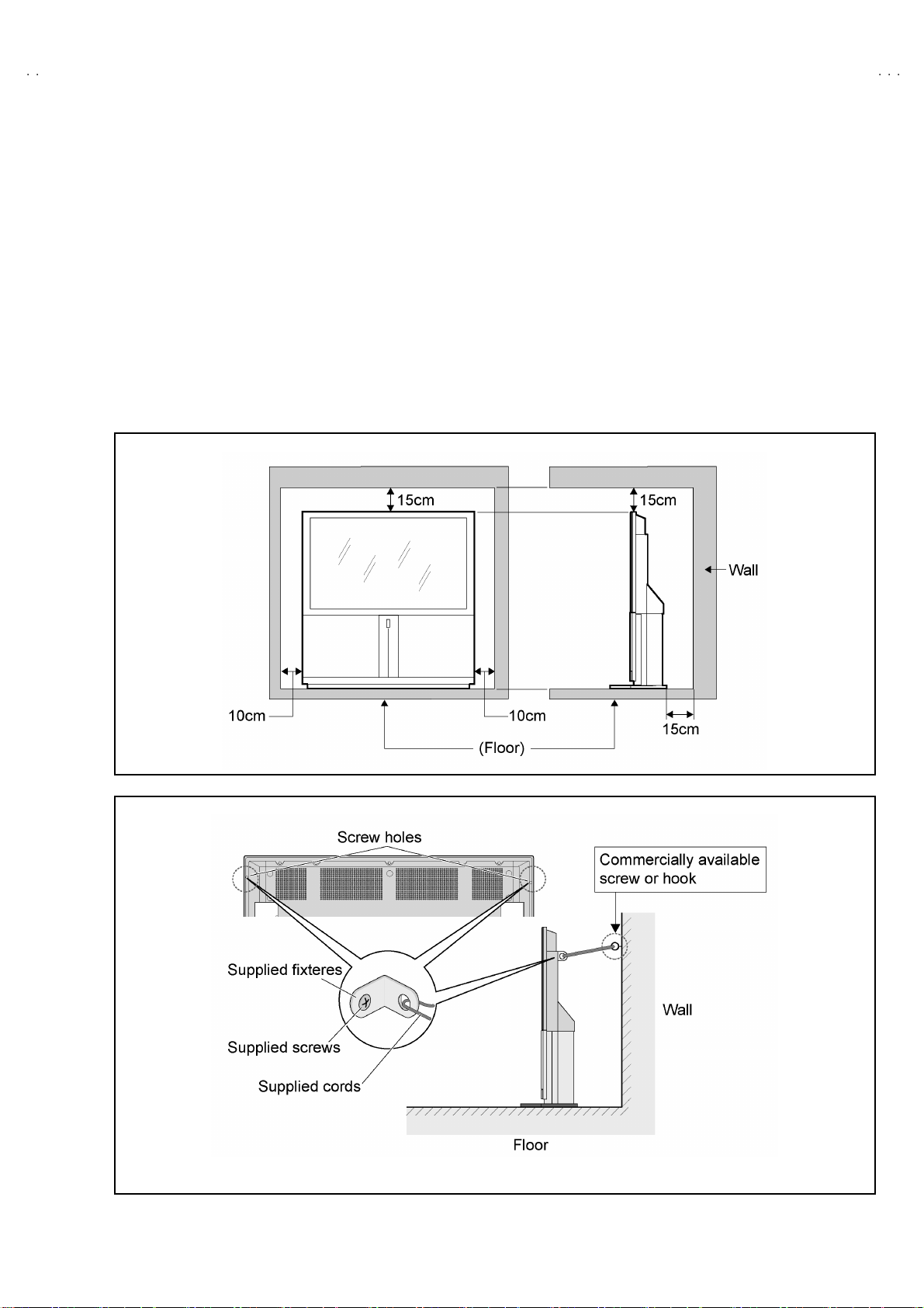
2. REQUIREMENTS FOR SETTING
The f ol l ow i ng m in imum sp ace mu st be kept wh en a PD P is
installed.
(3) Ins tal l in not du sty p lace. If dust co ver s th e a ir in ta ke h oles ,
inside ventilation effect will reduce. Then, it may damage the
inn er ci rcu it .
If the unit uses in such atmosphere, it will strongly require
regu l ar clean ing or main ten anc e.
No. 51955
11
Page 12

A
V42PD20ES
SPECIFIC SERVICE INSTRUCTIONS
PRECAUTIONS FOR PDP USE
1. PRE CAUTION DURING TRANSPORTATION
When this unit is delivered, the PDP body inside of the box will be
subject to constant of gravitation under the rough handling
(thr ow ing , dr opp in g, etc. ) ev en th ou gh a ri gid bo x is used.
In suc h a c as e, the PDP may b e da ma ged du ring tran sport ation .
In o rd er to a void an acc i d ent d ur i ng tr a ns p ort atio n, ca re mus t be
tak en to sel e ct a r eliab l e carrier. Onc e a relia ble carrier is select ed,
ad vis e them ho w to h an dle a PDP prop er l y d ur i ng tra nsp ortat i on.
In add ition, a PDP sho uld b e in sur ed for its p hys i cal da ma ge
before ship ment.
Thi s pr od uc t is fr ag ile bec aus e glass is wi d el y used . Thus the
follo win g r eq ui r em en ts fo r tr ans p or ta ti on s ho ul d be obs er ved.
(1) Do n't apply vibration and impact.
The glass of a PDP ma y be b ro ken when th e pac ka ge is
brought down on its side. When carrying the package, it must
alway s be ha ndle d w i th t wo p erson s w it h due c are n ot to a pp ly
vi br ati o n and imp act on the p ackag e.
(2) Do n't lay a PDP on its side.
A PD P s h ou ld al w ays b e placed uprig ht d ur i ng both
tr ans port ation a nd s afe keep i ng. Do n't la y it on its si de . The
p ane l of a PD P is very frag ile t o t he i mp act i n th e h or i zont al
directi on.
When a car car r ies a PDP , loa d it on b oar d th e car in para lle l
wit h th e mov i ng di r ect io n o f t he car . Don' t l a y seve ral PDP s
on e on t op an oth er.
During s af ekee pi ng , don 't la y mor e tha n tw o PD Ps on e on to p
an oth er e v en if they a r e kept u pr igh t.
2. RETANED-IMAGE AND BURN ING
(1) W hen t he s am e pat ter n is di s pl a yed c ontin uou sly for many
h our s, t he burn ing of th e screen is occu rre d in the sam e
mann er as for a CRT. T his will shorten the servic e life of a
PDP. I n orde r t o av o i d the b ur ni ng of th e s cr een, tu rn th e
display off wh en not neces sary. Also take such oth er
measu res as scr ol lin g the scr een an d using a sc re en save r. In
ad diti on , period ic all y d isp lay th e brigh tn es s re versal , t he
rever s a l t o t he c om ple me nt ary c ol ou r or th e i ns erti on of
animated image - all these will make the display on the screen
un if or m. Sinc e the hi gh er br i gh tn ess m ay cau se th e b urn ing,
us ers a re r eq ues t ed to us e n eut ra l colo ur s as much as
possible. Animated image will not cause the burning.
(2) W hen the scr ee n is switche d a fte r c ont in u ous di spla y, th e
reta in ed -i m ag e m ay be significan t beca use th e brigh tnes s of a
cer tain porti o n b ecom es hi gh er th an th at of oth er por tio ns.
Thi s is c ause d by a p heno me no n in wh ich a sur f ace elect rica l
disch ar ge of t he l i gh ted po rt ion i s m or e a c ti v at ed t ha n th e
n on- lig hted por ti o ns, r e s ul ti ng in h i gh er br i gh tness.
(3) This unit has functio ns such as “PIXEL SHIFT”, “COLOUR-
REVERSE” and “REFRESH”. They will reduce burning.
Please refer to th e in stru cti on book for d eta il.
3. INFR AR ED RAYS
Be caus e th e ne ar infrared r ays ( 80 0~1000 mm ) r a diat e fr o m t he
p ane l f ace , the ne ighb ori ng i nf rared ra y re mo te cont rolle rs,
infr ar e d c om mu ni cati o n sys tem s, etc. may m al f unc tion. In th es e
case s, tak e a me as u r e to pre ven t the t roub l e t o b e c aus ed b y
direct r ays (or r ef lecte d r ays) f r om t he scr ee n b y ch ang i ng t he
directi o n of the scr ee n fac e o r ke epin g a s afe dist ance b etw e en a
PDP and othe r de vic es .
4. OPTICAL FILTER (FRONT FILTER)
(1) Don' t exp ose the opti c a l f ilte r d ir ec tl y to th e su n for a lo ng
period of time.
Exposing directly to the sun for a long period of time may
ch ange th e s p ec ial prop er ty of th e op tical f ilter, re s ulti ng i n a
ch ange of co lo ur .
(2) Don' t wipe t he o ptica l filte r wi th s olvent s such as b enz e ne ,
thin ne r, etc.
Wiping t he optic al f ilt er w it h s o l ve nt s such as b enz e ne, th i nn er,
etc . m ay cau se ch ang e i n qu ali ty and pee l off the c oast in g on
th e su rf ace.
Lightl y wipe t he opt ic al fi lt er with a s o ft cloth w it h l ess f luff y (e. g.
pu re fl a nnel).
(3)
Be caus e the su rf ace of t he optica l fil ter i s fr agi l e, don' t scr ub o r
hit it wit h a hard materia l.
5. PRE CAUTION DURING CHANGING OF MONITOR
UNIT AR MOR PARTS
Extreme ca re mus t b e exer cised for a PDP whe n th e a r mor pa rt s
are c hange d.
(1) Sp ec i al att en ti on sh oul d be p aid no t to ap pl y pr essu re on th e
MO NI T OR U NIT gl ass surfac e dur in g t he w or k.
(2) Don' t t ouc h t he panel su rf ac e i n a ny way.
(3) W hen ch an gi ng t he M ONITOR UNIT arm or par ts ( re ar cover ,
fr on t p an el and o pti cal fi lter ), plac e t he p ane l ( PD P s i d e)
up side d own in pr i nc i ple . At thi s ti m e, a s u it ab le mat m us t b e
us ed so as to preve nt th e fron t s ide f r om dam a ging . Ho we ver,
exce ssi ve ly s of t ma teri al ( e. g. blan ket ) s h oul d not be us ed f or
this pur p ose in a ny wa y. If a blanket i s use d, th e s ur f ace of a
PDP is pr es surized by th e blank et when plac ing th e p anel
up side do wn.
Under such a c on dition , th e PDP m ay be b roken du rin g the
work.
6. OTHE R PRECAUTIONS
(1) Br ig h tne ss ch a nge in t h e scr een
In o rd er to sa ve t he power con sum ptio n, th e power is
con trolled ( w it h AP S f unction ) d epe nd ing on the brig htn ess of
th e scr een. For th is, the br i ght ness ma y c han ge aft er a s h or t
tim e wh en the p ictur e of th e s cr een i s ch ange d. Howev e r, this
ph en om en on is not a tr oubl e.
(2) Comp onent input setting
The component signals 1080i and 1035i are the same
fr eq ue nci es. S o, th e u nit d oes n ot d etec t th e s i gn al s
automatically.
In this c ase, set req uir ed s igna l by “HD SI GNAL MODE” in the
set up menu.
12
No. 51955
Page 13
A
S
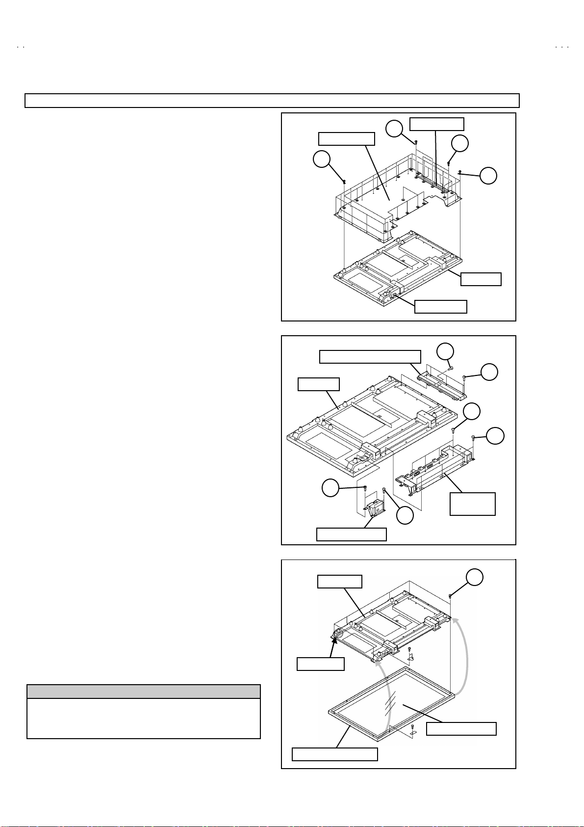
DISASSEMBLY PROCEDURE
U
U
SEPARATION
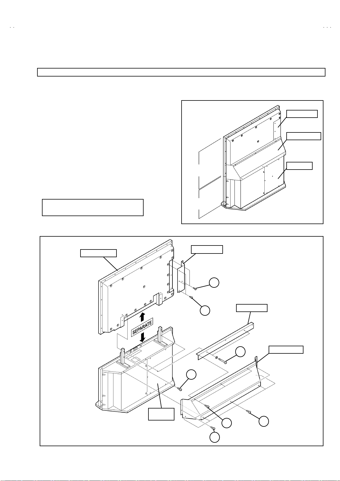
SEPARATING THE PDP MONITOR UNIT AND LOW ER BLOCK
[1] REMOVING THE BACK COVER
1. Rem ove the 5 screws marke d A a s sh own in Fig.2.
2. Rem ove the 2 screws marke d B a s sh own in Fig.2.
3. Rem ove the 3 screws marke d C a s sh own in Fig.2.
4. Remove the back cover toward you.
[2] RE M OVIN G THE SID E C OVER
5. Rem ove the 3 screws marke d D a s sh own in Fig.2.
6. Rem ove the 2 screws marke d E as shown in Fig.2.
[3] REMOVING THE BACK STAY
7. Remove the side cover.
8. Rem ove the 2 screws marke d F as shown in Fig.2.
[4] SEPARATING THE MONITOR UNIT LOWER BLOCK
9. Rem ove the 2 screws marke d G as sh ow n in F ig.2.
10 . Se para te the MO NI TOR UNIT and L OWER BL OC K
as s hown in Fig. 2.
* This separation should be performed by 2
or more persons.
MONITOR
NIT
LOWER
BLOCK
V42PD20E
SI DE COVER
BACK COVER
RECEIVER
MONI TOR UNIT
SI DE COVER
D
××××
(
G
(××××2)
3)
E
(×××× 2)
Fig. 1
BACK STAY
F
××××
(
2)
BACK COVER
RECEIVER
NIT
C
××××
(
3)
B
××××
(
2)
Fig. 2
No. 51955
A
(××××5)
13
Page 14

A
V42PD20ES
LOWER BLOCK
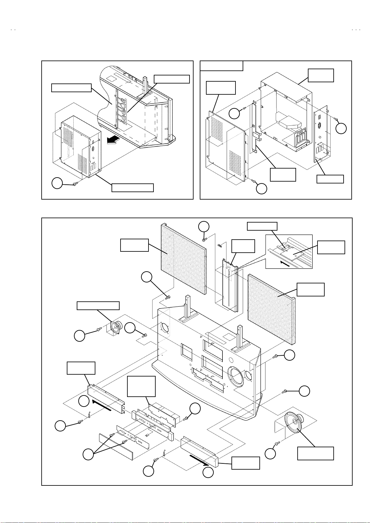
REMOVING THE LOWER BLOCK
[NOTE]
The peri p her y of the rece iver unit is a woo de n cabin et. Wh en th e
receiver unit is removed, hold it up slightly with both hands and
pu t a mat o r th e l i ke ( card boa r d, etc.) u nde r the recei v er un it s o
as to preve nt scr atch i ng the cab inet du r in g the remova l wor k.
Then remove the receiver unit by wit hdrawing it toward you.
[1] REMOVING THE RECEIVER UNI T
1. Rem ove th e 4 screws marked A as s h ow n i n Fig.3.
2. Slight ly rai se th e bo th si des o f th e rec eiver uni t b y hand an d
remove the receiver unit toward you.
*
Thus the connector should be securely inserted when the
receiver unit is installed again.
3. Unp lu g t he con nect or s fr om th e r e c eiver uni t.
4. Withdraw the receiver unit backward.
[2] REMOVING THE CASE COVER OF THE RECEIVER UNIT
• Take out th e RECEIVER UNIT.
1. Rem ove th e 10 screws marked A as sh own i n F ig .4.
2. Withdraw t he case cover toward you from ch assis case.
[3] REMOVING THE AV PLATE AND CHASSIS BEAM
• Take out th e RECEIVER UNIT.
• Take out th e CASE COVER.
1. Rem ove th e 6 screws marked B as s h ow n i n Fig.4.
2. Unp lu g t he con nect or s fr om th e AV PLATE
3. W ithdra w t he AV PLATE toward you .
4. Rem ove th e 2 screws marked C as shown in Fig. 4.
5. Withdraw t he chassis beam toward you from chassis case.
[4] REMOVING THE UNDER PANE L (L&R)
•
T ake out the RECEIVER UNIT.
1. Rem ove th e 2 screws marked D (L& R) as sh own in Fig.5.
2. Rem ove th e 4 screws marked H ( L& R) as sh ow n i n Fig.5.
3. As sh own Fig.5, remo ve th e un de r pa ne l (L& R ) i n th e arr ow
direction marked I.
[6] R EM OVIN G THE SP EAKER NET / CE NTER PANEL / FRONT
SW PWB / S W LEVER
1. R em ove th e 4 screws marked C (L& R si d e) as sh own in
Fig.5.
2. The n w it hdraw the SPEA KER NE T to ward you.
3. R em ove th e 4 screws marke d E as shown in Fig.5.
4. The n r emove th e C E NTE R PAN EL / FRONT SW PWB & SW
LE VER as sho wn in Fig.5.
[7] REMOVING THE SPEAKER
• Take ou t the SPEA KER NE T.
1. R em ove th e 4 screws marke d F as shown in Fig.5.
2. F ol low the sa me st eps when re mo ving th e oth er han d
sp eake r.
3. R em ove th e 4 screws marke d G as sh ow n in F ig.5.
CHECKIN G THE PW BOARD
1. To check the back side of the PW BOARD.
1) Pull out the chass is .
2) Erect the chas sis vertica lly so that you can easily check the
b ack side of the PW B OARD .
[CAUTION]
"
When er ect in g t he PW B OARD, b e caref ul so that th ere will be n o
con tact ing with ot her PW BOAR D .
"
Before turning ON power, make sure that the wire connector is
prop er l y con nected .0
"
When co nduc ti ng a ch eck w i th p ower su ppli ed , b e sure to c onfirm
th at t he EAR TH WI RE is connected to the PW BOA RD a nd
others PW BOAR D.
WIRE CLAMPIN G AND CABLE T Y ING
1. Be sure t o cl a mp th e wir e.
2. N ever r em o v e th e cable ti e use d f or tyi ng the wi re s to gethe r.
Should it be inadverten tly removed, be sure to tie the wires with a
new cable tie.
[5] REMOVING THE FRONT CONTROL PWB
•
T ake out the RECEIVER UNIT.
4. Rem ove th e 3(2+1) scr ews marked A as shown in Fig.5.
5. Rem ove the 6 screws marked B on th e F R ON T CO NTROL
PW B as sh ow n i n Fig.5.
* If nec essar y, t ak e off th e wire cl am p, con ne ctors, etc .
14
No. 51955
Page 15
A
S
SP EAKER BOX
CAS
CO
)
)
)
A
(××××4)
RECEIVER UNIT
Fig.3
CONNECT OR
RECEIVER UNIT
CASE
VE R
C
(××××2)
A
CHASSIS
BE A M
(×××× 10 )
Fig.4
V42PD20E
CHASSIS
E
B
(××××6)
AV PLA T E
H
(××××2)
SP EAKER (L&R
F
××××
(
4)
UNDER
I
SP EAKER
(×××× 2)
D
(×××× 1)
FRONT
C ONT RO L
PWB
CENTER
PANEL
SW LEVE R
FONT SW
PWB
E
(××××4)
C
SP EAKER
NE T (R
C
(×××× 2)
D
××××
(
1)
B
(×××× 6)
A
××××
(
2+1)
H
(××××2)
I
Fig.5
UNDER
PANEL (R
G
××××
(
4)
No. 51955
SUB WOOFER
SP EAKER
15
Page 16
A
V42PD20ES
MONITOR UNIT
REMOVING THE MONITOR UNIT
[1] REMOVING THE REAR COVER / SIDE COVER
* Take out th e MONITO R UNIT.
*
Take out the RECEIVER UNIT .
1. Rem ove th e 18 screws marked A as sh own i n F ig .1.
2. Rem ove th e 17 screws marked B as sh own i n F ig .1.
3. Rem ove th e 2 screws marked C as s h ow n i n Fig.1.
4. Rem ove th e 3 screws marked D as s h ow n i n Fig.1.
5. Withdraw the REAR & SIDE COVER toward you.
* If nec essar y, t ak e off th e wire cl am p, con ne ctors, p l ug. etc .
[2] RE M OVIN G THE SW PW B COVER
• Take out th e RE AR COVE R / SIDE C OVER.
1. Rem ove th e 2 screws marked A a s sh ow n i n Fig.2.
2. Rem ove th e 2 screws marked B as s h ow n i n Fig.2.
3. W ithdra w t he SW PW B CO VER to ward you .
[3] REMOVING THE SPEAKER / TERMINAL COVER
•
Take ou t th e RE AR COVE R / SIDE COVER.
•
Take ou t th e SW PW B C OV ER.
1. Rem ove th e 6 screws marked C as s h ow n i n Fig.2.
2. Rem ove th e 4 screws marked D as s h ow n i n Fig.2.
3. W i thdraw the S PE AKER an d TE RMINA L CO VER to ward
you.
REAR COVER
B
(××××17 )
INPUT TER M IN AL C OVER
PDP UNIT
C
××××
(
Fig.1
2)
SI DE COVER
POWER S W
F
D
(×××× 3)
PDP UNIT
(××××2)
D
A
××××
(
E
(××××5)
××××
(
18 )
4)
C
(××××6)
[4] RE M OVIN G THE IN PUT T ERMINAL CO VER
•
Take ou t th e RE AR COVE R / SIDE COVER.
1. Rem ove th e 5 screws marked E as shown in Fig.2.
2. Rem ove th e 2 screws marked F as shown in Fig.2.
3. Pu ll out the INPU T TE RMINAL COVE R back wa rd .
[5] REMOVING THE PDP UNIT
•
Take ou t th e RE AR COVE R / SIDE COVER.
•
Take ou t th e SW PW B C OV ER.
•
T ake out the TERMINAL COVER.
•
T ake out the INPUT TERMINA L COV ER.
1. Rem ove th e 6 screws marked A as s h ow n i n Fig.3.
2. Take o ut t he MONITOR UNIT f ro m the FR ONT PANEL
AS S’Y(wit h OP TICAL FI LTER) .
* The remo ve of P DP UNIT sh ou ld be per f or me d by 2 or mor e
persons.
CAUTION : Do not dama ge the gas in let
If t he gas in l et is dama ged, th e PDP UN IT mus t be re placed.
So extreme care should be taken not to damage the gas
inle t when y ou remove the PDP UNIT.
!!!!
B
××××
(
2)
SW PWB C OVER
PDP UNIT
GAS I NLET
FRONT PANEL ASS’Y
TERMINAL
COVER
A
(××××2)
Fig.2
A
(××××6)
OPTICAL FILTER
Fig.3
16
No. 51955
Page 17
A
S
REPLACEMENT OF MEMORY ICs
y
1. MEMORY ICs
This TV uses memor y IC. In the memory IC, th er e are memori zed data
for c orrec tly op erati n g t he vi deo and defl ec ti on circu i ts.
When r epl ac ing th e memory IC, b e su r e t o u se an IC w r it ten w it h t he
initial values of data.
2. PROCEDURES FOR REPLACING MEMORY ICs
PROCEDURE
SE RV I CE ME NU
1. IF 2. V/C
3. AUDIO 4. DEF
5. VSM PRESET 6. STATUS
7. PIP 8. - - -
9. SHIPPING (OFF) 0. BUS FREE
1-0 : S ELECT : EXITi
V42PD20E
(1) Power off
Switch the p ow er of f and di sco nnect t he pow e r pl u g.
(2) R epla ce ICs.
Be sure t o use a m em or y IC w r itt en wit h the in it ial set ting d ata.
(3) Powe r o n
Connect th e pow er p lu g and switc h t he pow e r on.
(4) Check and s et SY STEM CONSTANT SET
" The adjustment should not be done without signal.
1) Pr ess th e INFORMATI ON key and the MUTING key of the
REMO TE CONTROL UNIT simultaneous ly.
2) The SERVICE MENU screen of Fig. 1 will be displayed.
3) While th e S ERVIC E ME NU is dis pl a y ed, press t he
INFORM ATIO N key a nd MUTING key s imul t aneou sly, and th e
SYSTEM CONSTANT SET screen of Fig. 2 will be displayed.
4) Check th e se tting va lues of the S YSTEM CONSTA NT SET of
Tab le 1. If val u e is diff erent, selec t th e sett ing it em with th e
FUNCTION ▲▲▲▲ / ▼▼▼▼ key, a nd set th e c orrect value w ith th e
FUNCTION / key.
5) Pr ess the MENU(OK) key to memorize the setting value.
6) Pr ess the INFORMATION key, and re tur n to t he no rm al sc r e en.
Fig.1
SY STEM C O N STAN T S ET
1. DESTINATION
+ : STORE : EXIT
OK
E
i
Fig.2
2. DIGIPURE PRO
3. PIP
4. PI C & TEXT
5. TDA9178
6. FLAT
YE S
1 TUNER
YE S
YE S
YE S
REMOTE CONTROL UNIT KEY ASSIGNMENT
MUT ING
POWE R Ke
(5) Se tt in g of re ceive chann e ls
Se t th e r ec eiv e ch anne l.
For setting , r ef er to the OPE RATING INS TRUCTIONS.
(6) Setting of SERVICE MENU
Ve rif y the set ting it ems of the SE R VICE ME NU of Tab l e 2, and r es et
where n ecessary.
For setting , r ef er to the SE RVIC E ADJUSTMENTS.
(7) U ser se tting s
Check th e us er s ett ing values of T ab le 3, and i f s e tti ng valu e i s
diff erent , set th e c orrec t val u e.
INFORMATION
FUNCTION
▲/▼
ME NU
FUNCTION
/
For setting , r ef er to the OPE RATING INS TRUCTIONS.
No. 51955
17
Page 18
A
V42PD20ES
SETTING VALUE OF SYSTEM CONSTANT SET (TABLE 1)
Setting item Setting content Setting value
1. D ESTINATION E
2. Dig i Pur e YE S
3. PIP 1 TUNER
4. PIC & TEXT YE S
5. TD A917 8 YE S
6. FLAT YE S
EK EU EI
YE S NO
1 TUNER 2 TUNER
YE S NO
YE S NO
YE S NO
NO
SERVICE MENU SETTING ITEMS (TABLE 2)
Setting item Setting value Setting ite m Setting value
1. IF 1. VC O
2. ATT [ Do no t adjust]
2. V / C 1. R. GAIN
2. G. GAIN
3. B. GAIN
4. BRIGHT
5. CONTRAST
6. COLO UR
7. HUE
8. SHARP [ Don’t move]
9. VCO ADJUSTMENT
10 . VIDEO AGC [Don’t move ]
11 . SYNC S LICE [Don’t move]
12 . A MOV IE [ Don’t mo v e]
4. DEF 1. V-SHIFT
5. VS M PRESE T
COOL
NORMA L
WARM
2. V-SIZE
3. H-CENT
4. H-S IZ E
1. CONT.
2. BRIGHT
3. SHAR P
4. COLO UR
5. HUE
6. R . GAIN
7. G. GAIN
8. B. GAIN
3. AUDIO
[Do not a dju st]
1. ERR LI MIT
2. A2 ID THR
7. PIP
[Do not a dju st]
1. PIP VC O AD J
2. PIP VI D AGC
3. PIP SN C SL I
18
No. 51955
Page 19
A
S
USER SETTING VALUE (TABLE 3)
Setting item Setting value Setting item Setting value
SUB POWER ON VOLUME Appropriate sound volume
SHIPPING CHANNEL PR1 DISPLAY INDICATED
V42PD20E
PRES ET CH AN NEL
PICTURE SE TTING EX T SETTI NG
TINT (COLOUR TEMP.) NORMAL ID
PICTURE FEATURES FEATURES
DIGITAL VNR
Digi Pure
COLOUR S YST E M
4:3 AUTO ASPECT
PIP POS ITION
TONE
BALANCE
TV S PEAKER
3D SURROUND
See O PER ATING
INSTRUCTIONS.
AUT O
AUT O
TV : Ac co rd ing t o pr eset CH
EXT : AUTO
PA NO RA MI C
RIGHT BE LOW
SOUND SET TING INSTALL
CENTER
CENTER
L / R
OFF
ZOOM MODE PANORAMIC
BLANK
S-IN
DUBBING
SLEEP TIMER
BLUE BLACK
CHILD LO CK
DECODER (EXT-2)
LA NG UA G E
EDIT
BLANK
EXT- 1→EX T-2
OFF
ON
ID : No.0000, AL L CH : OFF
*
Press the “0” key in CHILD LOCK
menu to find to ID No.* ***.
ALL CH : OFF
ENGL ISH
PR CHANNEL ONLY
OTHERS : BLANK
No. 51955
19
Page 20
A
V42PD20ES
REPLACEMENT OF CHIP COMPONENT
! CAUTIONS
1. Avoid heating for more than 3 seconds.
2. Do n ot ru b the elect ro des an d the r esist p arts of the p att ern.
3. W hen r em oving a chip par t, mel t th e s older ad equately.
4. Do n ot reuse a ch ip p ar t afte r re mo v ing it .
! SOLDERING IRON
1. Use a hig h i ns ulatio n s ol der i ng i r on with a thi n poin ted e nd of it.
2. A 3 0 w s older i ng iron is r ec ommend ed for easily r em oving p ar ts.
!
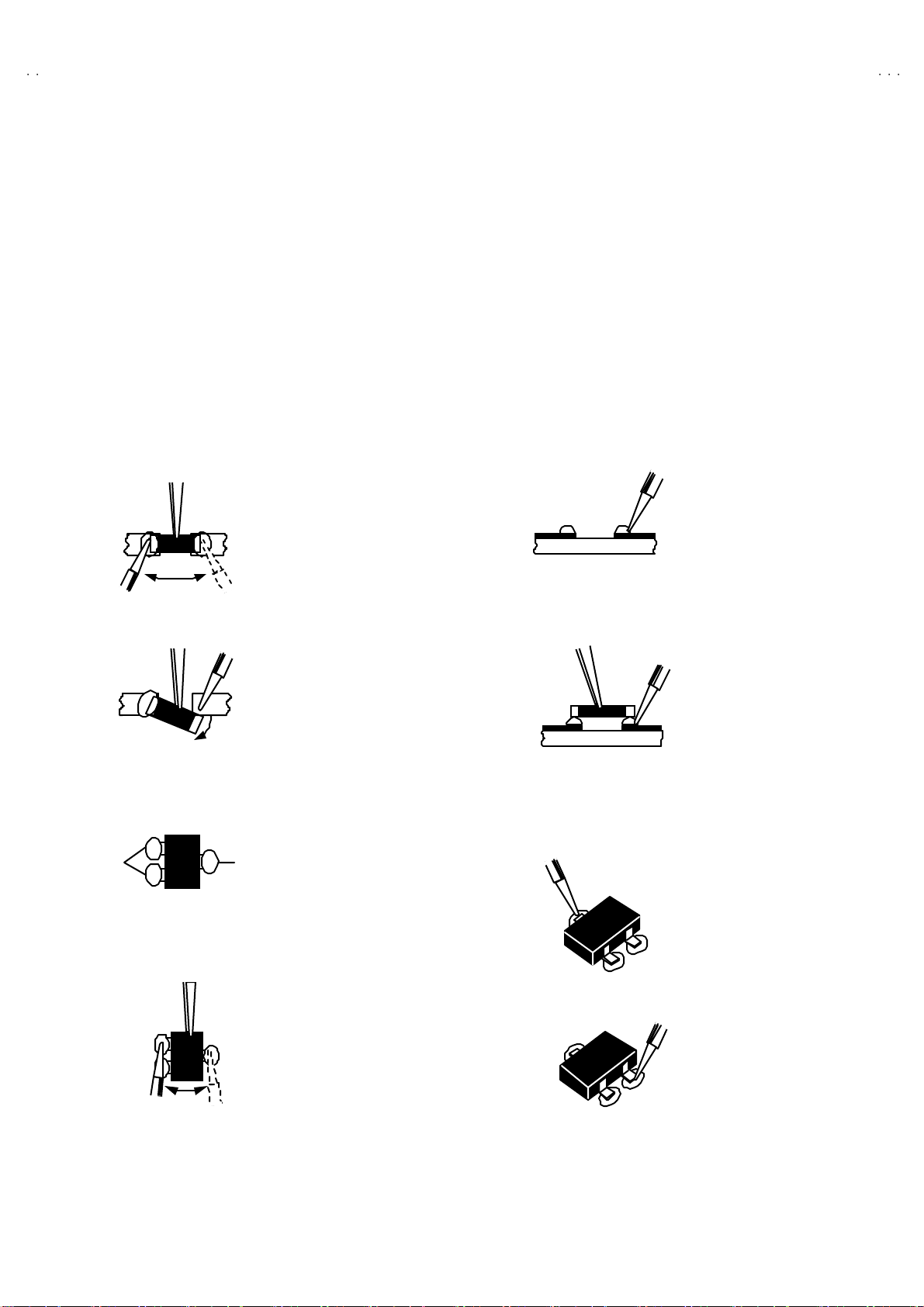
REPLACEMENT STEPS
1. How to remove Chip parts
####
Resi st o rs, capacitors , etc
(1) As sh own in the f ig ur e, pu sh th e pa rt w ith tw ee zer s and
alte rn at ely melt the s ol de r at eac h end.
(2) Sh if t with tweeze rs and r em ove th e c h i p p art.
#### Trans isto rs, d io des , va ria bl e r esist or s, etc
(1) Ap pl y e xt ra so ld er to eac h le ad .
2. How to install Chip parts
####
Resi st o rs, ca pacit ors , etc
(1) Apply solder to th e patt ern a s i ndicated in the fi g ure.
(2) Gr asp t he ch ip p art with tw ee z er s and pl ac e it on th e s old er.
The n hea t and me lt th e so lder a t both ends of t he chi p part.
#### Trans ist ors, diodes , va ria bl e r esistor s, etc
(1) Apply solder to th e patt ern a s i ndicated in the fi g ure.
(2) Grasp the ch ip p art wit h t weeze rs and p lace it on the s o l der .
(3) First s older lead A as indica ted in t he figure.
SOLDE R SO LD ER
(2) As sh own in the f ig ur e, pu sh th e pa rt w ith tw ee zer s and
alte rn at ely melt th e sol d er at each le ad . S hi ft an d r em ove the
chip part.
Note : A fte r re moving t he part, r emove rem ain ing solder fr o m the
pattern.
20
(4) The n solder le ads B and C .
No.51955
A
B
C
A
B
C
Page 21
A
S
SERVICE ADJUSTMENTS
BEFORE STARTING SERVICE ADJUSTMENT
1. Ther e ar e 2 w ays of ad ju st in g this TV: One is wi th t h e
REMOTE CONTROL UNI T and the other is the conventional
method using adjustment parts and components.
2. The setting (adjustment) using the REMOTE CONTROL
UNIT is made on the ba sis of th e initial se tting values . Th e
se tting va lu es whic h adjust the sc ree n to the o p t imum
condition can be different from the initial setting values.
3. Make s ur e th at conn ect i on i s c orrec t ly ma de t o AC p ower
source.
4. Tur n on th e pow e r of th e T V and m eas u r in g i ns tr um en t for
warmin g up f or at least 30 min ut es bef ore sta rt in g adju stm ent .
5. If th e r ec ei ve or i np ut sig nal is not sp eci fi ed , use t he m ost
ap pr op ri a te s ig na l f or a dj ust me nt.
6. Nev er tou ch p ar ts ( s uch as var i ab le r es ist ors, tr an s for m er s an d
condensers) not shown in the adjustment items of this service
adjustment.
7. Pr ep ar atio n f or ad j ustm en t (pr es etti n g)
Unles s oth erw is e sp eci fi ed in th e a dj us t ment it em s , p res e t th e
follo win g fu nct ions with th e REMOTE CONTROL UNIT
●
USER M ENU SE TT ING
TINT / CONTRAS T / BRIGHT
TR EBL E / BASS / BA LANCE CEN TER
V42PD20E
Setting Item Setting Position
Z OOM PA NO RA MI C
PICTURE MODE (VSM) NORMAL
/ SHARP / COLOUR
SLEEP TIMER OFF
ECO OFF
CENTER
MEASURING INSTRUMENT
AND FIXTURES
1. DC voltmeter (or digital voltmeter)
2. Oscilloscope
3. Sign al g en erat or (P attern g en erat or ( D igit al & Anal og) )
[PAL / S ECAM / NTSC]
4. Remote control unit
ADJUSTMENT ITEMS
< M ONI TO R >
!
Ch eck ing it em
•
Adju stment of PO WER VOL TAGE
< RE CE I VE R >
•
Checking of AFT CW VCO
!
VS M pr ese tt in g
•
Setting of VS M PR ESE T
!
V/C c ircu it adjust ment
•
Adjustmen t of WHI TE BA LANCE ( H i gh Li gh t)
•
Adju stment of SU B BR IGH T
•
Adjustment of CONTRAST
• Ad justm en t of SUB CO LOURⅠ
• Ad justm en t of SUB CO LOURⅡ
• Ad justm en t of SUB HUEⅠ
• Ad justm en t of SUB HUEⅡ
•
Check ing of MAIN COLOUR DECODER VCO
• Checking of SUB COLOUR DECODER VCO
! DEFLECTION circuit adjustment
•
Adju stment of V. POSITION
• Ad justm en t of V. SIZE
• Ad justm en t of H. PO SITIO N
• Ad justm en t of H. SI ZE
NOTE
This model (AV42PD20 ES) consist s of a MONITOR and a RECEIVER. However, the MONI TOR and RECEIVER cannot be activated
sep arat ely. T ryi ng the s epa ra te ac ti vation of th e MO NITOR o r RECEI VER may c ause a tr ou ble. Always tr y to ac ti vate th e MONITOR and
RECEIVE R as a uni t d ur i ng a s ervic e rep air.
No. 51955
21
Page 22
A
V42PD20ES
ADJUSTMENT PART LOCATIONS
!
RECEIVER
! MONITOR (PDP)
22
No. 51955
Page 23
A
V42PD20E
S
K
BASIC OPERATION SERVICE MENU
1. TOOL OF SERVICE MENU OPERATION
Operate the SERVICE MENU with the REMOTE CONTROL UNIT.
2. SERVICE MENU ITEMS
With the SERVI CE MENU, var i ou s sett ings ( ad ju s tm en ts) c an b e m ade , a nd th ey are b r oad ly classif i ed i n th e f ol lowing ite ms of set tings
(adjus tments ):
(1) 1. IF ・・・・・・・ ・・・・・・・・・・・・・ ・・・ This mode adjust s the se tting valu es o f th e IF circui t.
(2) 2.V /C
(3) 3.AUDIO ・・・・・・・ ・・・・・・・・・・・・ This mode adjusts the setting values of the multiplicity SOUND circuit.
(4) 4. DEF
(5) 5.V SM PRESE T ・・・・・・・・・・・・・ T hi s m ode adjust s th e in iti a l s ett in g va lues of CO OL, NORM AL and W ARM .
(VSM : Video Status Memory)
3. BASIC OPERATION OF SERVICE MENU
(1) How to enter SERVICE MENU
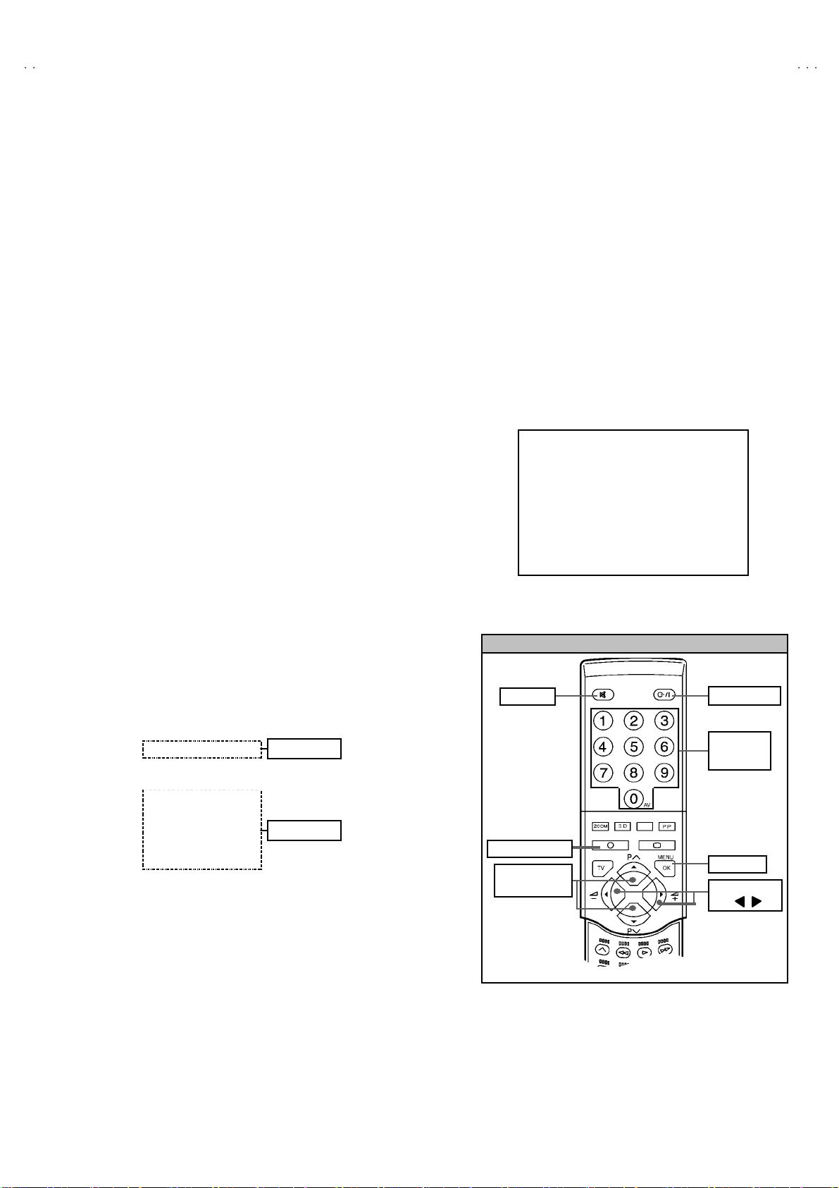
Press the IN FORM ATI ON key and th e MUTING key of the
(2) Selec tion of SUB MENU SCREEN
Press one of keys 1
SERVICE MENU
・・・・・・・ ・・・・・・・・・・・・・ ・・
・・・・・・・ ・・・・・・・・・・・・・ ・
REMO TE CONTROL UNIT (Fig. 2) simultaneously, and the
SERVICE MENU screen of Fig. 1 will be displayed.
~
5 (Fig. 2) of the REMOTE CONTROL
UNIT and select the SUB MENU SCREEN (See Fig. 3), form
the SERVICE MENU.
→
SUB ME NU
This mod e adjust s the se tting valu es o f th e VIDEO / CHROMA circu it.
This mod e adjust s the se tting valu es o f th e DEFLECTION cir cuit.
1. IF
2. V / C
3. AUDIO
4. DE F
No t t o ad just
5. VSM PRESE T
6. ST ATU S
7. PI P
8. - - -
No t t o ad just
9. SHIP PING (OFF )
0. BUS S F REE
SE RVICE MENU
SERVICE MENU
1. IF 2. V/C
3. AUDIO 4. DEF
5. VSM PRESET 6. STATUS
7. PIP 8. - - -
9. SHIPPING (OFF) 0. BUS FREE
1-0 : SELEC T : EXITi
Fig.1
REMOTE CONTROL UNI T KEY ASSIGNMENT
MUT ING
INFORMATION
FUNCTION
▲/▼
POWE R ke y
NUMBERS
(ten) key
ME NU/ O
FUNCTION
/
Fig.2
No. 51955
23
Page 24
A
V42PD20ES
)
SERVICE MENU FLOW CHAR T
Don't se lect under the adjustm ent
as this menu is s et in ON aft er the
inspection.
SUB MENU
SE RVICE MENU
SERVICE MENU
1. IF
3. AUD IO
5. VS M PR E S ET
7. PIP
9. SHIPPING(OF F)
1-0 : SELECT i : EXIT
2. V/C
4. DEF
6. ST ATUS
8. - - -
0. BUS FREE
Do no t adjust this Item.
1. V-SHIFT
2. V-SIZE
3. H -CENT
4. H -SIZ E
COOL
NORMAL
WARM
1. CONT.
2. BRIGHT
3. SHARP
4. COLOUR
5. HUE
6. R. GAIN
7. G. GAIN
8. B. GAIN
4. DEF
DE F F ULL
1. V- SHIFT
: STORE i : EXIT
OK
- / +
5. VS M PR E SET
VSM PRESET NORMAL
1.CONT
: STORE i : EXIT
OK
- / +
****DO NOT ADJUST
6. STATUS
STATUS
1.SOFT
: STORE i : EXIT
OK
- / +
*
**
**
Hz
** **
****
(****)
1.IF
IF SER VICE M ENU
1. VCO
2. AT T ON / OFF
1-2 : SELECT i : EXIT
1.VCO (CW
VCO (CW)
MAIN
TO O HIGH
ABOVE REF
JUST REF
BELOW REF
TO O LOW
**
**....**
****
**
****
MHz
i : EXIT
2. V/C
V/C PAL
1. R GAIN
- / +
: STORE i : EXIT
OK
****
Do no t adjust
this Item.
1. R . G AIN
2. G . GAIN
3. B . G AIN
4 . B R IG H T
5. C ONT.
6. C OLOUR
7. H UE
8. SHARP
9. VCO ADJ
10. VID AGC
11. SYNC SLI
12. A MO VIE
3. AUDIO
AUDIO
1. ERR LIMIT 0AH
C AD BITS =
: STORE i : EXIT
OK
* ***** **
1. ERR L IMIT
2. A2 ID THR
1. PIP VCO ADJ
2. PIP VID AGC
3. PIP S NC SL I
1.PIP VC O ADJ
: STORE i : EXIT
OK
- / +
7. PIP
PIP
*****
- / +
Fig.3
24
No. 51955
Page 25

A
S
(3) Setting methods
" Meth od of Set ting 1. IF as [V CO]
(The adju s tm ent sho ul d not b e done wi tho ut s ig na l.)
① 1 K ey ・・・・・・・ ・・・・・・・・・・・・・・・・・・ Se lect 1.IF.
② 1 K ey ・・・・・・・ ・・・・・・・・・・・・・ ・・・・ Select 1 . VC O (CW)
Check the arrow p osition b etwee n the “ABOVE REF. and BEL OW REF.
③ IN FORMATION K ey ・・・・・・・ ・・・・・ Retu rn t o the SERVICE MENU screen.
" Meth od of s ett in g 2.V/C, 4.DEF and 5.V SM PR ES ET .
① 2 ~5 K ey・・・・・・・ ・・・・・・・・・・・・・ ・・ Select one from 2. V/C , 4. DEF an d 5. VS M PRESE T.
② F UNCTION U P/ DOWN K ey ・・・・・・ Select s etting i tems.
③ FUNCTION LEFT/RIGHT K ey・・・・ Set (ad just) th e se tti ng valu es o f th e setting it ems.
④ MENU (OK) Key ・・・・・・・ ・・・・・・・・ Memorize the setting value.
(Bef ore st orin g t he sett in g values in m emor y, do not pres s th e C H , T V, POWE R ON / OFF k e y
- if you do, t he valu es wi ll n ot be s tor ed i n me mo r y. )
⑤ IN FORMATION K ey ・・・・・・・ ・・・・・ Ret urn to the SE RVICE ME NU scree n.
" Do n ot adjust 3. AUDIO, 6 . S TATU S, 7. PIP, 8. --- , 9 . S HIPPI NG (O FF) and 0. BUS FREE fu nction.
V42PD20E
(4) Rele as e of SER V ICE M E NU
1) After complet ing the ad justmen t, r et urn to the S ERVICE ME NU, then again press th e INFORMATION key to return to the normal
screen.
No. 51955
25
Page 26
A
V42PD20ES
INITIAL SETTING VALUE OF SERVICE MENU
1. Ad justment of the SERVICE MENU is made on the basis of the initial setting values ; however, the new setting values which
set the screen in its optim um condition may differ from the initial setting.
2. Do no t change the initial setting values of th e setting (Adjustment) items not li sted in “ ADJUSTM ENT”.
1.IF
SETTING ITEM Initial setting value
1.V CO
2.ATT O N/OFF Do n ot adjust th i s item.
2.V/C (VIDEO / CHROMA) ( is adjus t ment not to requ i re d )
Colour syst em
Setting item
1. R. GAIN -15
2. G. GA IN -15
3. B. GAIN -15
4. BR IG HT 20
5. CONT RAST 0
6. COLOUR -10
7. HUE 01 1
8. SHARP 0
9. VCO ADJUSTMENT Automatically optimized after adjustment
10 . VI DEO AGC 00
11 . SY NC SL ICE +07
12 . A. MOVIE 01
PA L SE C AM NT SC
Prop er valu e b y adjustmen t.
Se e “ad j ustm en t of VCO ” co ntents
Initial setting value
3.AUDIO (Do not adjust)
Setting item Variable range
1. ERR LIMIT 00H~FFH 10
2. A2 ID THR 00H~FFH 19
4.DEF ( is adjust ment not to requ ire d )
Setting item
1. V-SHIFT -03
2. V-SIZ E 00
3. H-CENT -06
4. H-S IZE 00
26
Initial setting value
(Fixed value )
VAL UE
FULL
50 Hz p
No. 51955
Page 27
A
S
5.VSM PRESET
VS M pr ese t mo d e
COOL NORMAL WARM
Setting item
1. CONT . +12 + 12 00
2. BRIG HT 00 00 00
3. SHARP -12 -12 -12
4. COLOUR 00 00 -01
5. HUE 00 00 00
6. R . G AIN 00 00 00
7. G. GAIN 00 0 0 00
8. B. G AIN 00 00 00
7.PIP ( i s adjust ment not to requ i re d )
Initial setting value
Setting item
PAL SE CAM
V42PD20E
NT S C
1. PIP VC O ADJ
2. PIP VI D AGC 00
3. PIP SN C SLI +07
No. 51955
27
Page 28
A
V42PD20ES
JU S
(AFC)TOO LO
this ite
arro
ADJUSTMENT
■ MONI TOR
Item
Ad j ust men t
of POWER
VOLTAGE
Measuring
instrume nt
DC
voltmeter
Signal
generator
Test point Adjustment part Description
TP-1 (+5V)
TP-2 (####)
TP-3 (+ 17 0V)
TP-4 (+ 60V)
VR1 (+5)
VR3 (+17 0V )
VR4 (+60 V)
**** Ad just ment of Vs(+17 0V ) v olt age.
1. Input the colour bar si g nal t o RGB inpu t te rminal .
2. Con nect the d ig ital vol t meter across TP3 an d TP 2 ( #).
3. Ad jus t th e VR 3 to s et th e v ol ta ge wi thi n ± 1V of th e volta ge (V s
as s hown on th e SE RIAL L ABEL) de signe d f or the PDP mo dul e.
****
Adjustment of Vd(+60V ) voltage.
1. Input the colour bar si g nal t o RGB inpu t te rminal .
2. Con nect the d ig ital vol t meter across TP4 an d TP 2 (#).
3. Ad jus t th e VR 4 to s et th e v ol ta ge wi thi n ± 1V of th e volta ge (V s
as s hown on th e SE RIAL LA BEL) de signe d f or the PDP mo dul e.
**** Ad just ment of +5V v o lt ag e.
1. Input the colour bar si g nal t o RGB inpu t te rminal .
2. Con nect the d ig ital vol t meter across TP1 an d TP 2 ( #).
3. C onf irm that the vol ta ge o f th e TP 1 an d TP2 (#) ha ve bec ome
5.1 V±0 .1V . If not , adjust t he VR1 a t th e + 5V ADJ of the POW ER
PWB so that the voltage become 5.1V±0.1V.
■RECEIVER
Check ing of
AFT CW VCO
Remote
control unit
IF SERVICE MENU
1. V CO
2. A TT O N/O FF
1-2 : SELECT
VCO M ENU
VCO(CW)
TOO H IGH
ABOVE REF
JUST REF
BELOW REF
TOO LOW
1. IF
Fig.1
Fig.2
i : EXIT
****
MHz
i : EXIT
1.V CO
Do no t sel ect
YE LLOW
" Und er n orm a l c ondi tions, no ad just me nt is r e quired
confirmation adjustment.
1. Se lect 1 .IF from the SERV ICE M ENU.
2. The n se lect 1.VCO from th e 1.IF S ERVICE ME NU (Fig.1) .
3. Recei v e an y bro adc ast ( 55 .75M Hz or 21 6.00MHz i s b est) .
4. In th e VCO ad jus tm ent scree n, th e yell ow al l ows poi nt ( Fig.2) to
th e ch ar ac t ers. C hec k the yellow allow posi tio n wh er e poi nt ed to
the character from “ABOVE REF” to “BELLOW REF” (Fig.2 &
m
Fig.3).
*Th e arr ow p os i ti on menu AF C volt age leve l.
V
TOO HIGH
w
ABOVE R EF.
T REF.
BELO W R EF.
W.
t
Fig.3
28
No. 51955
Page 29
A
S
VSM PR ESET S ETTI NG
V42PD20E
Item
Setting of
VS M PRESET
Measuring
instrume nt
Remote
control unit
Test point Ad justment part Description
1. CONT.
2. BR I G HT
3. SHARP
4. COLOUR
5. HUE
6. R. GAIN
7. G. GAIN
8. B. GAIN
1. Pr es s t he MEN U ( OK) key an d s elect COOL m od e wit h th e
remote control unit.
2. Se lect 5 .VSM P R ESET fr om th e S ER VIC E ME NU.
3. Ad ju s t the FUNCTIO N ▲ / ▼ a nd / key to b rin g th e set
val u es of 1.CON T ~ 8 .B G AIN to th e in itia l settin g valu es as
sh own i n the b efore table.
4. Pr ess the ME NU key a nd m em or iz e the s et va l ue.
5. Respectively select the VSM PRESET mode for NORMAL and
WAR M, an d make simi l ar a dj ust me nt as in 3 abo ve.
6. Press the MENU (OK) key and memorize t he set value .
★ Refer to OPERATING INSTRUCTIONS for the PICTURE
MO DE .
V/C (VIDEO/CHROMA) CIRCU IT ADJUSTMENT
●●●● The setting (adjustment) using the REMOTE CONTROL UNIT is made on the basis of the initial setting values.
●●●● The setting values which adjust the screen to the optimum condition can be different from the initial setting values.
Item
of WHITE
BALANCE
(Hi gh-Light)
Ad j ust men t
of
SUB BRIGHT
Ad j ust men t
of
SUB
CONTRAST
Measuring
instrume nt
Signal
generator
Remote
control unit
Remote
control unit
Remote
control unit
Test point Ad justment part Description
1. R. GAIN
2. G. GAIN
4 .BR IG HT 1. R eceive any br o adc ast.
5.CONTRAST 1. R eceive a PAL colo ur ba r s i gna l.
" Set the PICTURE MODE to NORMAL.Ad j ust men t
1. R eceive a bl ack a nd w hi te si gn al ( colour off ).
2. Select 2 . V/ C from th e S ERVICE MENU.
3. Modi f y 1.R . GAIN an d 2.G .GA IN valu e to s et th e w hi te b al a nc e
( high ligh t ).
4. Press the MENU (OK) key and memorize the set value .
5. C ha nge t he c on trast and b rig htn ess u p and d ow n with t he
remote c on trol u nit fr om Low –l i ght to Hig h –light , and chec k t ha t
th e trac kin g of th e wh it e bala nce is good.
2. Se lect 2 .V/C f rom the SE RVICE MEN U .
3. Select 4.BRIGHT with the FUNCTION ▲/▼ key.
4. Set the initial setting value with t he FUNCTION / key.
5. If th e brightn ess i s not the best with the initial se tting value,
make fine adjustment until you get the best brightness.
6. Press the MENU (OK) key and memorize the set valu e.
2. Sw i tch t he s ub po wer SW to OF F & O N.
3. Se lect 2 .V/C f rom the SE RVICE MEN U .
1. Select 5.CONTRAST with the FUNCTION ▲/▼ ke y.
5. Set the initial setting value with t he FUNCTION / key.
6. If the co ntrast is not the best with th e in itial se tting val ue, make
fine adjustment until you get the best contrast.
7. Press the MENU (OK) key and memorize the set valu e.
No. 51955
29
Page 30
A
V42PD20ES
Item
Ad j ust men t
of SUB
COLOURⅠⅠⅠⅠ
Measuring
instrume nt
Remote
control unit
Test point Ad justment part Description
6.COLOUR
SUB POWER key
[Method of adjustm ent without measuring instrument]
< PAL COLOUR >
1. Recei v e PA L broad cast.
2. Se le ct 2 .V/C f rom the SE RVICE MENU .
3. Se lect 6 .COLOUR with th e FUNCTION ▲/▼ key.
4. Set the initial s etting value for PAL COLOUR wit h the
FUNCTION / key.
5. If the co l our i s no t th e be st w it h th e i ni ti a l se t v alu e, m ake fine
adjustment until you get the best colour.
6. Press the MENU (OK) key and memorize the set value.
< SECAM COLOUR >
1. R eceive a SECAM b r oadc as t.
2. M ak e fi ne adj us tm en t of SEC A M COL OU R in th e sa me m an ner
as f or a bove.
FUNCTION
NUMBERS key
( INFORMATION ) key
i
MENU ( OK ) key
▲▲▲▲/▼▼▼▼
& / key
< NT SC 3. 5 8 C OL O UR >
1. Input a NTSC 3.58MHz CO MPOSITE V IDEO signal from the
EXT t erminal .
2. M ake s imi l ar fi ne adjus tm ent of N T SC 3. 58 CO LOUR i n t he
sam e mann er as f or a bo ve .
< NT SC 4. 4 3 C OL O UR >
1. Input a NTSC 4.43MHz COMPOSITE VIDEO s ignal from the
EXT t erminal .
2. Make similar fine adjustment of 4.43 COLOUR in the same
mann er as fo r abo v e.
30
No. 51955
Page 31

A
V42PD20E
S
(+)
5%
0%
5%
(+)
Item
Ad j ust men t
of SUB
COLOUR ⅡⅡⅡⅡ
7
Measuring
instrume nt
Signal
generator
Oscilloscope
Remote
control unit
W
CyYeG
Test point Ad justment part Description
[Method of adjustm ent using measur ing instrument]
< PAL COLOUR >
1. R eceive a PAL fu ll f ield co lour b ar sign al ( 75 % whi te ).
2. Se lect 2 .V/C f rom the SE RVICE MEN U .
3. Select 6 .COLOUR with th e FUNCTI ON ▲/▼ key.
4. Se t t he i ni t ial se tting value of PAL CO LOUR with t he
FUNCTION / key.
5. C on nect th e osc illosc ope be twee n TP -R a nd TP-E
6. Ad jus t PAL C OL OUR a nd br i n g th e val ue of (A) in th e t o
illustration (Fig.1) to -140mV(W-R).
7. Press the MENU (OK) key and memorize t he setting value.
Mg
Fig. 1
TP-R
####
TP-E(
[CRT
SOCKET
PWB ]
R
B
)
(W- R)
A
6.COLOUR
(-)
7
0%
Ye Mg
W
Cy G B
R
Fig. 2
< SECAM COLOUR >
1. R eceive a SECAM fu l l fi el d c olou r bar sig nal ( 7 5% whit e) .
2. Set the initial setting value of SECAM COLOUR with the
FUNCTION / key.
3. Ad jus t S ECAM COL OUR an d br in g th e val u e of (A) in the
illustration (Fig.2) to -140mV(W-R).
4. Press the MENU (OK) key and memorize t he setting value.
(W- R)
B
< NT SC 3. 5 8 C OL O UR >
(-)
1. Inp ut a N T SC 3.5 8MH z C OM POSI TE VIDEO sign al ( fu ll fi el d
colo ur bar with 75% whit e) from th e EXT terminal.
2. Set the init ial s etting value of NTSC 3.58 COLOUR wit h the
FUNCTION / key.
3. Ad just NTSC 3. 58 CO LOUR a nd br in g t he valu e o f (B) of th e
illustration (Fig.1) to -140mV(W -B).
4. Press the MENU (OK) key and memorize t he setting value.
< NT SC 4. 4 3 C OL O UR >
1. W hen NTSC 3 .58 adj ust me nt h as don e, t hen NTS C4.4 3
adjustment will be automatically set at the respective values.
No. 51955
31
Page 32

A
V42PD20ES
g
0%
(+)
(
)
(
)
Item
Ad j ust men t
of
SUB HUEⅠⅠⅠⅠ
Ad j ust men t
of
SUB HUEⅡⅡⅡⅡ
Measuring
instrume nt
Remote
control unit
Signal
generator
Oscilloscope
Remote
control unit
75%
Test point Ad justment part Description
7. HUE
TP-R
TP-E(#### )
[CRT
SOCKET
PWB]
W
Ye
M
7. HUE
B
R
0
(-)
[Method of adjustm ent without measuring instrument]
< NTSC 3.58 HUE >
1. Inp ut a N T SC 3.5 8MH z C OM POSI TE VIDEO signa l (f ul l f iel d
colo ur bar with 75% whit e) from th e EXT terminal.
2. Se lect 2 .V/C f rom the SE RVICE MEN U .
3. Se le c t 7 .HU E wi th th e FU NCT IO N ▲/▼ key.
4. Set the initial setting value of NTSC 3.58 HUE with t he
FUNCTION / key.
5. If you c ann ot g et the b est HUE wit h th e i ni ti al s ett ing val u e,
make fine adju stm en t un ti l you g et the bes t HUE.
6. Press the MENU (OK) key and memorize t he set value.
< NTSC 4.43 HUE >
1. When NTSC 3.58 is set, NTSC 4.43 will be automatically set at
the respective values.
[Method of adjustm ent using measur ing instrument]
< NTSC 3.58 HUE >
1. Inp ut a N T SC 3.5 8MH z C OM POSI TE VIDEO signa l (f ul l f iel d
colo ur bar with 75% whit e) from th e EXT terminal.
2. Se lect 2 .V/C f rom the SE RVICE MEN U .
2. Se le c t 7 .HU E wi th th e FU NCT IO N ▲/▼ key.
4. Set the initial setting value of NTSC 3.58 HUE with t he
FUNCTION / key.
5. C on nect th e osc illosc ope be twee n TP -R a nd TP-E
6. Adju s t N T SC 3 .5 8 HUE t o bring th e val u e of (B) in the
illustration to 30mV(W-Mg).
7. Press the MENU (OK) key and memorize t he setting value
Cy
GB
< NTSC 4.43 HUE >
1. When NTSC 3.58 is set, NTSC 4.43 will be automatically set at
the respective values.
32
No. 51955
Page 33

A
V42PD20E
S
Item
Check ing
of
MAIN COLOUR
DECODER VCO
Check ing
of
PIP COLOUR
DECODER VCO
MAIN
PICTURE
Measuring
instrume nt
Signal
generator
Remote
control unit
Signal
generator
Remote
control unit
Test point Ad justment part Description
9. VC O 1. Input a PA L hal f col ou r bar sign al ( 7 5% whit e) fr om the EX T
terminal.
2. Se lect 2 . V/ C from the SERVICE ME NU.
1. Se lect 9 . VCO adjustm ent with t he FUNCTION ▲/▼ key.
4. Pr es s the ME NU ( OK) ke y th en aut omati ca lly opt imi zed .
7. PI P 1. Select 7 . PIP f rom t he SERVI C E M ENU.
2. R eceive r a PA L h al f colou r bar ( 75% whit e) si g nal f or t he
SUB- PIC T U RE ( R ight- S id e pi ctur e)
3. Se le ct 1 . PIP VOC ADJ. w ith the F UNCTIO N ▲/▼ key.
4. Pr es s the ME NU ( OK) ke y th en aut omati ca lly opt imi zed .
SUB PICTURE
No. 51955
33
Page 34

A
V42PD20ES
DEFLECTION CIRCUIT ADJUSTMENT
"
When the FULL mode has been established, the setting of other modes will be don e automatically.
Ho wever, if the picture quality has not been optimized, adjust each mod e again, respectively.
" There are 5 aspe ct mo d es ( ①①①①FULL, ②②②②PANORAMIC, ③③③③ REGULAR, ④④④④16:9 ZOOM , ⑤⑤⑤⑤14:9 ZOOM) of the adjustment depending
upon the kind of signals.
"
The adjustment using the remote control unit is made on the basis of the initial setting values.
" The setting values whi ch adj ust the screen to the optimum condition can be different from the initial setting val ues.
Item
of V. POS ITION
Ad j ust men t
of V. SIZ E
Measuring
instrume nt
Signal
generator
Remote
control unit
Signal
generator
Remote
control unit
Test point Ad justment part Description
1. V- S HI FT
A
●Set th e A SPE CT MO DE to FULL.Ad j ust men t
1. Receive a circle pattern signal.
2. Se le ct 4 .DEF f rom t he SERVI CE M ENU .
3. Se le ct 1.V-SHIFT with t he FUNCT ION ▲/▼ key.
4. Adjust V-S HIFT to make A = B .
5. Check t he ad jus tm en t con di ti o n in o th er asp ect m od e. I f it i s a
wrong condition, re-adjust in “FULL” mode with 1. V-SHIFT.
6. Press the MENU (OK) key and memorize t he set value.
B
2.V-SI ZE 7. Receive a cross hat ch si g nal.
8. Select 2.V-SIZE and set the initial setting value t o zero(0).
9. Ad ju st t he V -SI Z E to t he vert ic al scr ee n si ze of th e picture
becomes the value given figure.
10. Press the MENU ( OK) key and memorize the set value.
Sc re en
size
( 96%)
34
Pi ct ur e
size
1 00%
No. 51955
Page 35

A
V42PD20E
S
(C)
(D)
Item
Adjustment of
H. POSIT ION
Measuring
instrume nt
Signal
generator
Remote
control unit
Test point Ad justment part Description
3 .H - CE NT. 11 . Recei ve a cross hat ch with circl e p att ern sign al.
12 . Se le ct 3 .H -CE NT an d set th e ini t ia l s ett i ng v alue .
13 . Ad ju s t H - CE NT to ma ke C=D.
14. Press the MENU (OK) key and memorize the set value.
Ad j ust men t
of H. SIZE
Signal
generator
Remote
control unit
Screen size(96%)
Picture size 100%
4.H-SIZE 15 . Recei ve a cross hat c h p att er n s ign al .
16 . Se le ct 4 .H - SIZE and se t th e i n iti a l s ett in g value t o zero(0 ).
17. Adjust the H-SIZE and make sure that the horizontal screen size
of th e p ict ure i s in the ta ble bel l ow.
18. Press the MENU (OK) key and memorize t he set value.
19 . Inp ut th e NT SC V IDEO s i gn al ( 60 Hz ) fr om t he EX T t er min al,
an d m ake su re that the hor i zon tal scr ee n si ze of the p ict ure
becomes the value given figure.
20. Press the MENU (OK) key and memorize the s et value.
No. 51955
35
Page 36

A
V42PD20ES
TROUBLESHOOTING
MONITOR UNIT DOES NOT WORK
(Whe n t he LED blinks with R ED and GREE N al t ernat ive ly)
1) Pres s the RE SE T SW whi le th e power is tur n ed off.
2) Then, wait for two sec onds after turning the power on.
3) Tun e t he power off af ter two s econ ds.
4) Rel ea s e t he RESET PW .
5) The main unit of PDP will be ac tivated when the power is tuned on.
MONI TOR UNIT
RECEIVER INPUT
TERMINAL
AUDIO IN
(sub woofer)
RESE T SW
36
No. 51955
Page 37

A
V42PD20E
S
PARTS LIST
CAUTION
! The pa rts identified b y the ! symbol are i m por t ant for t he s afe ty. W hene ver r epl acing the se par ts, be sure t o use s pec if i ed o nes to se cure
the safety .
!
T he pa rts n ot ind ic ated i n this P ar ts L ist a nd tho se whic h ar e fi l l ed with l i nes in the Parts No. c olumns will not be supplied.
! P. W. Board Ass'y will not be sup plied, but thos e which are filled with the Parts No. in the Parts No. columns will be supplied.
ABBREVIATIONS OF RESISTOR S, CAPACITORS AND TOLERANCES
RESISTORS CAPACITORS
C R Carbon Resistor C CAP. Ceramic Capacitor
F R Fusible Resistor E CAP. Electrolyt ic Capacitor
P R Plate Res istor M CAP. Mylar Capacitor
V R
HV R High Voltage Resistor MF CAP. Metalized Film Capacitor
MF R Metal Film Resistor MM CAP. Metalized Mylar Capacitor
MG R Metal Glazed Resistor MP CAP. Metalize d Polystyrol Capacitor
MP R M etal Plate Resi sto r PP CA P. Po lyp ropylen e Ca pa citor
OM R M etal Oxi de F ilm Resistor
CMF R Coating Metal Film Resistor TF CAP. Thin Film Capacitor
UNF R Non-Flammable Resi s to r MPP C AP . Metalize d Pol y pr op ylene Cap acito r
CH V R Chip Variable Resistor TAN. CAP. Tantalum Capacit or
CH MG R Chip Metal G lazed Resistor CH C CAP. Chip Ceramic Capac itor
COMP . R C om posit ion Re s ist or BP E CAP . Bi- Pola r E lectroly ti c Ca pacit or
LP TC R
Variable Res istor
Linear P ositiv e T emperat ur e C o effici e nt
Resistor
HV CAP. High Voltage Capacitor
PS CAP.
CH AL E CAP. Chip A luminum Electrolytic Capacitor
CH AL BP CAP.
CH TAN. E CAP.
Polystyrol Capacitor
Chip A lum i num B i- Po lar Cap acitor
Chip T ant alum Elec trol y tic Cap ac itor
CH AL BP E CAP.
Chip T ant alum Bi-Po l ar El ec tr o lytic C a pac itor
TOLERANCES
FGJ KMNRHZ P
±
1%
±
2%
±
5%
±
10 %
±
20 %
±
30 %
+30%
-10%
No. 51955
+50%
-10%
+80%
-20%
+100 %
-0%
37
Page 38

A
V42PD20ES
CONTENTS
!!!!
USING PW BOARD & REMOTE CONTROL UNIT
!!!!
EXPLOD ED VIEW PARTS LIST
!!!!
EXPLOD ED VIEW
!!!!
PRINTED WIRING BOARD PARTS LIST
"
MAIN PW BOARD ASS'Y
"
POWER PW BOARD ASS' Y
"
LINE FILTER PW BOARD ASS’Y
"
FRONT CONTRO L PW BOARD ASS'Y
"
FRONT SW PW BOARD ASS'Y
"
SPEAKER TERMINAL PW BOARD ASS'Y
"
MICOM PW BOARD ASS'Y
"
AV SW PW BOARD ASS'Y
"
100Hz PW BOARD ASS'Y
"
SIDE JACK PW BOARD ASS'Y
!
REM OT E CONT ROL U NI T PA RT S LIST ・・・・・・・ ・・・・・・・・・・・・・ ・・・・・・・・・・・・・・・・・・・・・・・・・・・・・・・・ ・・・・・・・・・・・・ ・・・・・・・ ・・・ 49
!
PA CK I N G ・・・・・・・ ・・・・・・・・・・・・・ ・・・・・・・・・・・・ ・・・・・・・・・・・・・・・・・・・・ ・・・・・・・・・・・・・・・・・・・ ・・・・・・・・・・・・・ ・・・・・・・・・・・・ ・・・・・・・ ・ 50
!
PACKING PARTS LIST・・・・・・・ ・・・・・・・・・・・・・ ・・・・・・・・・・・・・・・・・・・ ・・・・・・・・・・・・・ ・・・・・・・・・・・・・・・・・・・ ・・・・・・・・・・・・・・・・・・・・ 50
・・・・・・・ ・・・・・・・・・・・・・ ・・・・・・・・・・・・・・・・・・・ ・・・・・・・・・・・・・・・・・・・・・・・・・ ・・・・・・・ ・・・・・・・・・・・・・ ・・・・・・・ 39
・・・・・・・ ・・・・・・・・・・・・・ ・・・・・・・・・・・・・・・・・・・ ・・・・・・・・・・・・・・・・・・・・・・・・・ ・・・・・・・ ・・・・・・・ 39
・・・・・・・ ・・・・・・・・・・・・・ ・・・・・・・・・・・・・・・・・・・ ・・・・・・・・・・・・・・・・・・・・・・・・・ ・・・・・・・ ・・・・・・・・・・・・・ ・・ 42
・・・・・・・ ・・・・・・・・・・・・・ ・・・・・・・・・・・・・・・・・・・ ・・・・・・・・・・・・・・・・・・・・・・・・・ ・・・・・・・ ・・・・・・・・・・・・
・・・・・・・ ・・・・・・・・・・・・・ ・・・・・・・・・・・・ ・・・・・・・・・・・・・・・・・・・・ ・・・・・・・・・・・・・・・・・・・ ・・・・・・・・ 45
・・・・・・・ ・・・・・・・・・・・・・ ・・・・・・・・・・・・・・・・・・・ ・・・・・・・・・・・・・・・・・・・・・・・・・ ・・・・・・・ ・・ 45
・・・・・・・ ・・・・・・・・・・・・・ ・・・・・・・・・・・・ ・・・・・・・・・・・・・・・・・・・・ ・・・・・・・・・・・・・・・・・・・ ・・・・・・・・・
・・・・・・・ ・・・・・・・・・・・・・ ・・・・・・・・・・・・・・・・・・・ ・・・・・・・・・・・・・・・・・・・・・・・・・ ・・・・・・・ ・・・・・・・・・・・・・
・・・・・・・ ・・・・・・・・・・・・・ ・・・・・・・・・・・・・・・・・・・ ・・・・・・・・・・・・・・・・・・・・・・・・・ ・・・・・・・ ・・・・・・・・・・・・・ ・ 47
・・・・・・・ ・・・・・・・・・・・・・ ・・・・・・・・・・・・・・・・・・・ ・・・・・・・・・・・・・・・・・・・・・・・・・ ・・・・・・・ ・・・・・・・・・・・・・ ・ 48
・・・・・・・ ・・・・・・・・・・・・・ ・・・・・・・・・・・・ ・・・・・・・・・・・・・・・・・・・・ ・・・・・・・・・・・・・・・・・・・ ・・・・・・・・・
・・・・・・・ ・・・・・・・・・・・・・ ・・・・・・・・・・・・ ・・・・・・・・・・・・・・・・・・・・ ・・・・・・・・・・・・・
・・・・・・・ ・・・・・・・・・・・・・ ・・・・・・・・・・・・・・・・・・・ ・・・・・・・・・・・・・・・・・・・・・・・・・ ・・・・・ 45
~~~~
~~~~
38
40
41
44
45
46
49
USING PW BOARD & REMOTE CONTROL UNIT
Model
PW B AS S' Y
MAIN PWB SMF-1101A- U2
POWER PWB SMF-9101A-U2
LIN E F ILTER PWB
FRONT CONTRO L PWB
FRONT SW PWB SMF-8302A-U2
SPEAKER TERMIN AL PWB
MICOM PWB
AV SW PWB SMF0S301A-U2
100Hz PWB SMF0Z301A-U2
FRONT JACK PWB SMF0J301A-U2
REM OTE CO NTROL U NIT
AV42PD20ES
SMF-9102A-U2
SMF-8301A-U2
SMF-8303A-U2
SMF0M301A-U2
RM-C59-1C
38
No. 51955
Page 39

A
V42PD20E
S
EXPLODED VIEW PARTS LIST(
Ref.No. Part No. Part Name Description
!
!
V01 QLE0016-001 P.D.P.
1 LC11294-001A-U BACK COVER
2 QYSDSF4016M TAP SCREW (×2)
3 QYSDSP4016M SCREW (×3)
4 LC11299-001B-U WOOD CABI
5 LC20805-001C BACK STAY
6 QYSSSP4040N SCREW (×2)
7 LC11293-001-U BACK COVER
8 QYSBSAG4018M TAPPING SCREW (×5)
9 QYSBSBG4016M TAPPING SCREW (×3)
10 LC30789-002B-U WARNING LABEL
!
11 LC21119-001A-U RATING LABEL
!
!
12 LC21024-001A-U RATING LABEL
ⅠⅠⅠⅠ
)
EXPLODED VIEW(ⅠⅠⅠⅠ)
!
V01
12
!
11
!
1
3
(×3)
2
(×2)
4
5
7
6
(×2)
!
10
8
(×5)
9
(×3)
No. 51955
39
Page 40

A
V42PD20ES
EXPLODED VIEW PARTS LIST(
Ref.No. Part No. Part Name Description
!
!
13 QMPL200-055-K POWER CORD
14 QAM0378-001 A/V CABLE
15 WJJ0334-001A E-SI C WIRE C-C
16 WJJ0335-001A E-SI C WIRE C-C
17 QYSBSAG4018M TAPPING SCREW (×4)
18 LC11295-001A-U CHASSIS CASE
!
19 QNC0093-001 AC OUTLET
20 LC21023-001A-U CHASSIS BEAM
21 LC11296-001A-U CHASSIS CASE TOP
22 QYSBSB3008M TAPPING SCREW (×10)
24 LC11297-001A-U AV PLATE
25 QYSBSB3008M TAPPING SCREW (×6)
26 CE42112-002 PALJ CONNECTOR
27 QNC0085-002 AC INLET (with WASHER & NUT)
!
!
28 QSW0699-001 SEESAW SWITCH
29 CHGY0017-0B-UK E-COAXIAL ASSY
30 LC11067-001C SPEAKER NET (×2)
31 LC40312-004A RUBBER WASHER (×8)
32 LC41037-002A JVC MARK
33 LC20787-002A CENTER PANEL
34 LC31494-002A ACCESORRY LENS
35 LC31493-001B POWER KNOB
!
36 LC41042-001A LENS
!
37 LC41097-001A LED SHADE
38 LC20786-001A STAND (×2)
39 QYSPSAG4025M SCREW (×4)
40 QYSBSAG4018M TAPPING SCREW (×2)
41 QAS0107-001 SPEAKER (×2)
42 QAS0108-001 SPEAKER
43 LC31497-001B SIDE CAP
44 LC31495-001A UNDER PANEL(R)
45 LC11069-002A CONTROL BASE
46 CM48229-00A-C DOOR LATCH
47 LC31498-002B CONTROL SHEET
48 LC11068-002A DOOR
!
49 LC31495-002A UNDER PANEL(L)
50 LC31497-002B CAP
51 QQR0491-002 CORE FILTER (×7)
ⅡⅡⅡⅡ
)
EXPLODED VIEW(
!
13
14
15
16
51
ⅡⅡⅡⅡ
)
!
1819
4
21
20
22
(×10 )
23
29
26
24
!
28
!
27
26
40
17
(×4)
No. 51955
25
(×6)
Page 41

A
S
33
!
35
37
!
36
30
39
(×2)
34
38
31
(×4)
32
33
V42PD20E
31
(×4)
50
49
41
(×2)
!
48
47
40
45
46
51
(×2)
51
(×4)
30
38
39
(×2)
40
42
44
43
No. 51955
41
Page 42

A
V42PD20ES
PRINTED WIRING BOARD PARTS LIST
■■■■MAIN P.W. BOARD ASS’Y (SMF-1101A-U2)
!
Symbol No. Part No. Part Name Description
RESISTOR
R1002-03 NRSA63J-473X MG R 47kΩ 1/16W J
R1004-05 NRSA63J-101X MG R 100Ω 1/16W J
R1008-09 NRSA63J-0R0X MG R 0.0Ω 1/16W J
R1101-02 NRSA63J-0R0X MG R 0.0Ω 1/16W J
R1103 NRSA63J-222X MG R 2.2kΩ 1/16W J
R1104 NRSA63J-102X MG R 1kΩ 1/16W J
R1105 NRSA63J-561X MG R 560Ω 1/16W J
R1106 NRSA63J-331X MG R 330Ω 1/16W J
R1107 NRSA63J-0R0X MG R 0.0Ω 1/16W J
R1108 NRSA63J-102X MG R 1kΩ 1/16W J
R1109-11 NRSA63J-101X MG R 100Ω 1/16W J
R1151 NRSA63J-101X MG R 100Ω 1/16W J
R1153 NRSA63J-101X MG R 100Ω 1/16W J
R1155 NRSA63J-101X MG R 100Ω 1/16W J
R1157 NRSA63J-101X MG R 100Ω 1/16W J
R1301-02 NRSA63J-101X MG R 100Ω 1/16W J
R1303 NRSA63J-273X MG R 27kΩ 1/16W J
R1304 NRSA63J-103X MG R 10kΩ 1/16W J
R1305 QRK126J-101X C R 100Ω 1/2W J
R1306 QRK126J-101X C R 100Ω 1/2W J
R1307 QRK126J-101X C R 100Ω 1/2W J
R1308-10 NRSA63J-750X MG R 75Ω 1/16W J
R1311 NRSA63J-153X MG R 15kΩ 1/16W J
R1312 NRSA63J-563X MG R 56kΩ 1/16W J
R1314 NRSA63J-221X MG R 220Ω 1/16W J
R1315-17 NRSA63J-101X MG R 100Ω 1/16W J
R1318 NRSA63J-103X MG R 10kΩ 1/16W J
R1321-22 NRSA63J-0R0X MG R 0.0Ω 1/16W J
R1337-39 NRSA63J-101X MG R 100Ω 1/16W J
R1351 NRSA63J-152X MG R 1.5kΩ 1/16W J
R1352 NRSA63J-182X MG R 1.8kΩ 1/16W J
R1353 NRSA63J-562X MG R 5.6kΩ 1/16W J
R1354 NRSA63J-152X MG R 1.5kΩ 1/16W J
R1355 NRSA63J-822X MG R 8.2kΩ 1/16W J
R1356 NRSA63J-332X MG R 3.3kΩ 1/16W J
R1357-59 NRSA63J-473X MG R 47kΩ 1/16W J
R1360-62 NRSA63J-273X MG R 27kΩ 1/16W J
R1363-65 NRSA63J-561X MG R 560Ω 1/16W J
R1366-68 NRSA63J-102X MG R 1kΩ 1/16W J
R1369-71 NRSA63J-122X MG R 1.2kΩ 1/16W J
R1372-74 NRSA63J-101X MG R 100Ω 1/16W J
R1375 NRSA63J-822X MG R 8.2kΩ 1/16W J
R1391-93 NRSA63J-152X MG R 1.5kΩ 1/16W J
R1394-97 NRSA63J-332X MG R 3.3kΩ 1/16W J
R1398 NRSA63J-472X MG R 4.7kΩ 1/16W J
R1401 NRSA63J-332X MG R 3.3kΩ 1/16W J
R1402 NRSA63J-103X MG R 10kΩ 1/16W J
R1403 NRSA63J-331X MG R 330Ω 1/16W J
R1404 NRSA63J-221X MG R 220Ω 1/16W J
R1405 NRSA63J-151X MG R 150Ω 1/16W J
R1406 NRSA63J-392X MG R 3.9kΩ 1/16W J
R1407 NRSA63J-221X MG R 220Ω 1/16W J
R1408 NRSA63J-101X MG R 100Ω 1/16W J
R1409 NRSA63J-103X MG R 10kΩ 1/16W J
R1410 NRSA63J-152X MG R 1.5kΩ 1/16W J
R1491 NRSA63J-332X MG R 3.3kΩ 1/16W J
R1492 NRSA63J-103X MG R 10kΩ 1/16W J
R1501 NRSA63J-0R0X MG R 0.0Ω 1/16W J
R1504 NRSA63J-102X MG R 1kΩ 1/16W J
R1511 NRSA63J-472X MG R 4.7kΩ 1/16W J
R1512 NRSA63J-0R0X MG R 0.0Ω 1/16W J
R1513 NRSA63J-103X MG R 10kΩ 1/16W J
R1515 NRSA63J-0R0X MG R 0.0Ω 1/16W J
R1516 NRSA63J-103X MG R 10kΩ 1/16W J
R1521 NRSA63J-182X MG R 1.8kΩ 1/16W J
R1522 NRSA63J-332X MG R 3.3kΩ 1/16W J
R1523 NRSA63J-0R0X MG R 0.0Ω 1/16W J
R1524 NRSA63J-152X MG R 1.5kΩ 1/16W J
Symbol No. Part No. Part Name Description
!
RESISTOR
R1525 NRSA63J-332X MG R 3.3kΩ 1/16W J
R1526 NRSA63J-221X MG R 220Ω 1/16W J
R1527 NRSA63J-101X MG R 100Ω 1/16W J
R1528 NRSA63J-102X MG R 1kΩ 1/16W J
R1591 NRSA63J-0R0X MG R 0.0Ω 1/16W J
R1592 NRSA63J-332X MG R 3.3kΩ 1/16W J
R1593 NRSA63J-182X MG R 1.8kΩ 1/16W J
R1595 NRSA63J-222X MG R 2.2kΩ 1/16W J
R1596 NRSA63J-104X MG R 100kΩ 1/16W J
R1604 NRSA63J-104X MG R 100kΩ 1/16W J
R1605 NRSA63J-473X MG R 47kΩ 1/16W J
R1606 NRSA63J-273X MG R 27kΩ 1/16W J
R1607 NRSA63J-104X MG R 100kΩ 1/16W J
R1609 QRK126J-103X C R 10kΩ 1/2W J
R1610-12 NRSA63J-223X MG R 22kΩ 1/16W J
R1613 NRSA63J-561X MG R 560Ω 1/16W J
R1614 NRSA63J-153X MG R 15kΩ 1/16W J
R1615 NRSA63J-104X MG R 100kΩ 1/16W J
R1616-17 NRSA63J-333X MG R 33kΩ 1/16W J
R1618-19 NRSA63J-103X MG R 10kΩ 1/16W J
R1620-21 NRSA63J-334X MG R 330kΩ 1/16W J
R1623 NRSA63J-223X MG R 22kΩ 1/16W J
R1630 QRK126J-2R2X C R 2.2Ω 1/2W J
R1632 NRSA63J-104X MG R 100kΩ 1/16W J
R1671 NRSA63J-0R0X MG R 0.0Ω 1/16W J
R1673 NRSA63J-225X MG R 2.2MΩ 1/16W J
R1674 NRSA63J-223X MG R 22kΩ 1/16W J
R1675 NRSA63J-272X MG R 2.7kΩ 1/16W J
R1677 NRSA63J-0R0X MG R 0.0Ω 1/16W J
R1678 NRSA63J-153X MG R 15kΩ 1/16W J
R1680-81 NRSA63J-101X MG R 100Ω 1/16W J
R1701-02 NRSA63J-103X MG R 10kΩ 1/16W J
R1703-04 NRSA63J-102X MG R 1kΩ 1/16W J
R1705-08 NRSA63J-103X MG R 10kΩ 1/16W J
R1711-12 NRSA63J-101X MG R 100Ω 1/16W J
R1715 NRSA63J-102X MG R 1kΩ 1/16W J
R1716-17 NRSA63J-0R0X MG R 0.0Ω 1/16W J
R1721-23 NRSA63J-102X MG R 1kΩ 1/16W J
R1751 NRSA63J-561X MG R 560Ω 1/16W J
R1752 NRSA63J-102X MG R 1kΩ 1/16W J
R1772-76 NRSA63J-221X MG R 220Ω 1/16W J
R1951 QRK126J-220X C R 22Ω 1/2W J
CAPACITOR
C1001 NCB31HK-222X C CAP. 2200pF 50V K
C1002 QETN1HM-106Z E CAP. 10µF 50V M
C1004 NCB31CK-104X C CAP. 0.1µF 16V K
C1005 QETN1CM-108Z E CAP. 1000µF 16V M
C1006 NCB31HK-103X C CAP. 0.01µF 50V K
C1007 QETN1HM-106Z E CAP. 10µF 50V M
C1009 NCB31CK-104X C CAP. 0.1µF 16V K
C1010 QETN1HM-106Z E CAP. 10µF 50V M
C1101 NCB31CK-104X C CAP. 0.1µF 16V K
C1102 QETN1HM-106Z E CAP. 10µF 50V M
C1103 NCB31CK-104X C CAP. 0.1µF 16V K
C1104 QETN1CM-107Z E CAP. 100µF 16V M
C1105 QETN1HM-106Z E CAP. 10µF 50V M
C1106-07 NCB31CK-104X C CAP. 0.1µF 16V K
C1111 NCB31HK-103X C CAP. 0.01µF 50V K
C1116 NCB31HK-472X C CAP. 4700pF 50V K
C1117-18 NCB31HK-103X C CAP. 0.01µF 50V K
C1119-20 NDC31HJ-2R0X C CAP. 2.0pF 50V J
C1121 NCB31HK-103X C CAP. 0.01µF 50V K
C1122-23 NDC31HJ-102X C CAP. 1000pF 50V J
C1124-25 QETN1HM-106Z E CAP. 10µF 50V M
C1126 NCB31CK-104X C CAP. 0.1µF 16V K
C1127 QETN1HM-106Z E CAP. 10µF 50V M
42
No. 51955
Page 43

A
V42PD20E
S
Symbol No. Part No. Part Name Description
!
CAPACITOR
C1128 NCB31CK-104X C CAP. 0.1µF 16V K
C1129 NCF31AZ-105X C CAP. 1µF 10V Z
C1130 QETN1HM-106Z E CAP. 10µF 50V M
C1151-54 NCF31AZ-105X C CAP. 1µF 10V Z
C1155-56 NDC31HJ-102X C CAP. 1000pF 50V J
C1301 QETN1CM-107Z E CAP. 100µF 16V M
C1302-03 NCB31CK-104X C CAP. 0.1µF 16V K
C1305-09 NCB31CK-104X C CAP. 0.1µF 16V K
C1310 QETN1AM-228Z E CAP. 2200µF 10V M
C1311 NCB31CK-683X CHIP CAP. 0.068µF 16V K
C1312 NDC31HJ-271X CER.CAP. 270pF 50V J
C1313-15 NCB31HK-223X C CAP. 0.022 µF 50V K
C1316-18 NCB31HK-103X C CAP. 0.01µF 50V K
C1320 QETN0JM-228Z E CAP. 2200µF 6.3V M
C1321-23 NCB31HK-223X C CAP. 0.022 µF 50V K
C1331-33 QETN1CM-477Z E CAP. 470µF 16V M
C1337 QETN1EM-476Z E CAP. 47µF 25V M
C1338 QETN1CM-107Z E CAP. 100µF 16V M
C1349-51 QETN1HM-106Z E CAP. 10µF 50V M
C1352 QETN1EM-476Z E CAP. 47µF 25V M
C1401 NCB31EK-333X C CAP. 0.033µF 25V K
C1491 NCB31EK-473X C CAP. 0.047 µF 25V K
C1501-02 NDC31HJ-150X C CAP. 15pF 50V J
C1510 QETN1HM-106Z E CAP. 10µF 50V M
C1511 QETN1CM-107Z E CAP. 100µF 16V M
C1512 NCB31CK-104X C CAP. 0.1µF 16V K
C1513-14 NDC31HJ-471X C CAP. 470pF 50V J
C1522 QETN1EM-476Z E CAP. 47µF 25V M
C1523 NCB31CK-104X C CAP. 0.1µF 16V K
C1564 NCB31CK-104X C CAP. 0.1µF 16V K
C1591 NDC31HJ-471X C CAP. 470pF 50V J
C1596 NCB31CK-104X C CAP. 0.1µF 16V K
C1602-03 QFV71HJ-684Z MF CAP. 0.68µF 50V J
C1604-05 NCB31CK-104X C CAP. 0.1µF 16V K
C1606-07 QETN1CM-227Z E CAP. 220µF 16V M
C1608-09 QETM1EM-228 E CAP. 2200µF 25V M
C1610 QETN1HM-106Z E CAP. 10µF 50V M
C1612 QETN1HM-106Z E CAP. 10µF 50V M
C1613 NCF31AZ-105X C CAP. 1µF 10V Z
C1614 QETN1EM-476Z E CAP. 47µF 25V M
C1615 NCF31AZ-105X C CAP. 1µF 10V Z
C1616-17 QETN1HM-107Z E CAP. 100µF 50V M
C1621 QETN1HM-106Z E CAP. 10µF 50V M
C1622 QETN1EM-476Z E CAP. 47µF 25V M
C1623 NCF31AZ-105X C CAP. 1µF 10V Z
C1624 NCB31HK-103X C CAP. 0.01µF 50V K
C1671 QENC1HM-475Z BP E CAP. 4.7µF 50V M
C1672 QETN1HM-475Z E CAP. 4.7µF 50V M
C1673 QETN1HM-106Z E CAP. 10µF 50V M
C1674 NCB31HK-103X C CAP. 0.01µF 50V K
C1675 QETN1CM-107Z E CAP. 100µF 16V M
C1676-77 QETN1HM-106Z E CAP. 10µF 50V M
C1678 QENC1HM-475Z BP E CAP. 4.7µF 50V M
C1679 QETN1HM-106Z E CAP. 10µF 50V M
C1680 NCB31HK-472X C CAP. 4700pF 50V K
C1681 NCB31EK-273X C CAP. 0.027µF 25V K
C1682 QETN1HM-105Z E CAP. 1µF 50V M
C1683 QETN1CM-107Z E CAP. 100µF 16V M
C1684-85 NCF31AZ-105X C CAP. 1µF 10V Z
C1686-89 QETN1HM-106Z E CAP. 10µF 50V M
C1701 QETN1HM-106Z E CAP. 10µF 50V M
C1702 NCB31CK-563X CHIP CAP. 0.056 µF 16V K
C1751 NCB31CK-104X C CAP. 0.1µF 16V K
C1752-54 NCB31AK-474X C CAP. 0.47µF 10V K
C1755 NCB31CK-104X C CAP. 0.1µF 16V K
COIL
L1001 QQL244K-270Z PEAKING COIL
L1002-03 QQL244K-100Z COIL 10µH K
L1004 NQL092K-100X COIL 10µH
Symbol No. Part No. Part Name Description
!
COIL
L1101 QRN143J-0R0X C R 0.0Ω 1/4W J
L1102 QQL244K-4R7Z COIL 4.7µH K
L1112 QRN143J-0R0X C R 0.0Ω 1/4W J
L1301-02 NQL092K-1R5X INDUCTOR
L1501 QQL244K-180Z COIL 18µH K
DIODE
D1314-20 MA111-X SI.DIODE
D1593 MA111-X SI.DIODE
D1602-04 MA111-X SI.DIODE
D1608 MA111-X SI.DIODE
D1609 MA3051/M/-X ZENER DIODE
D1610-11 MA3270/H/-X ZENER DIODE
D1612-13 MA3150/M/-X ZENER DIODE
D1614 MA111-X SI.DIODE
D1771-74 MA3056/M/-X ZENER DIODE
D1951 1SR35-400A-T5 SI.DIODE
TRANSISTOR
Q1101-02 2SC2412K/QR/-X SI.TRANSISTOR
Q1301-03 2SC1740S/QR/-T SI.TRANSISTOR
Q1304-05 2SC2412K/QR/-X SI.TRANSISTOR
Q1306 2SA1037AK/QR/-X SI.TRANSISTOR
Q1307-09 2SC2412K/QR/-X SI.TRANSISTOR
Q1310-12 2SA1037AK/QR/-X SI.TRANSISTOR
Q1313 DTC124EKA-X DIGI.TRANSISTOR
Q1401-03 2SC2412K/QR/-X SI.TRANSISTOR
Q1501 2SC2412K/QR/-X SI.TRANSISTOR
Q1591 2SA1037AK/QR/-X SI.TRANSISTOR
Q1592 2SC2412K/QR/-X SI.TRANSISTOR
Q1601 2SA1037AK/QR/-X SI.TRANSISTOR
Q1604-05 2SA1037AK/QR/-X SI.TRANSISTOR
Q1606 DTC124EKA-X DIGI.TRANSISTOR
Q1607 DTC323TK-X DIGI.TRANSISTOR
Q1608 2SA1037AK/QR/-X SI.TRANSISTOR
Q1609-10 DTC323TK-X DIGI.TRANSISTOR
IC
IC1101 MSP3415DQGB3GHX I.C.(MONO-ANA)
IC1301 SDA9380 I.C.(M)
IC1303 TC4053BF/N/-XE I.C.(DIGI-MOS)
IC1501 TC74HC4538AF-X I.C.(DIGI-MOS)
IC1502 TC4053BF/N/-XE I.C.(DIGI-MOS)
IC1601 TDA2052V I.C.(MONO-ANA)
IC1602 BA4558F-X I.C.(M ONO-ANA)
IC1671 AN5285K I.C.(MONO-ANA)
IC1672 NJM2701M-X I.C.(MONO-ANA)
IC1701 JLC1562BF-X I.C.(DIGI-MOS)
IC1751 MAX3232CPE I.C.(MONO-ANA)
OTHERS
C1112 NRSA63J-0R0X MG R 0.0Ω 1/16W J
CN1002 QGA2501C1-11 W TO B CONNE
J1601 QNN0281-002 PIN JACK
K1001 NQR0389-003X FERRITE BEADS
K1101-02 NQR0389-003X FERRITE BEADS
K1301 NQR0413-003X BEADS CORE
LC1102 NQR0431-001X EMI FILTER
LC1301-03 NQR0431-001X EMI FILTER
TU1001 QAU0270-001 TUNER
X1101 CE42546-001Z CRYSTAL
X1501 QAX0549-001Z CRYSTAL
No. 51955
43
Page 44

A
V42PD20ES
■■■■POWER P.W. BOARD ASS’Y (SMF-9101A-U2)
!
Symbol No. Part No. Part Name Description
RESISTOR
R9902 QRF054K-3R3 UNF R 3.3Ω 5W K
!
R9903 QRF074K-5R6 UNF R 5.6Ω 7W K
R9904 QRL029J-683 OM R 68kΩ 2W J
R9909 QRL029J-683 OM R 68kΩ 2W J
!
R9910 QRZ9017-4R7 F R 4.7 Ω 1/4W J
R9911 QRE121J-152Y C R 1.5kΩ 1/2W J
R9913 QRT029J-R33 MF R 0.33Ω 2W J
R9914 QRX01GJ-3R3 MF R 3.3Ω 1W J
R9915 QRE141J-681Y C R 680Ω 1/4W J
R9916 QRE141J-332Y C R 3.3kΩ 1/4W J
!
R9932 QRZ9017-470 F R 47 Ω 1/4W J
R9933 QRE121J-272Y C R 2.7kΩ 1/2W J
R9934 QRE121J-564Y C R 560kΩ 1/2W J
R9935 QRE141J-472Y C R 4.7kΩ 1/4W J
R9936 QRX01GJ-3R9 MF R 3.9Ω 1W J
R9937 QRE121J-681Y C R 680Ω 1/2W J
R9941 QRE121J-331Y C R 330Ω 1/2W J
R9942 QRE121J-471Y C R 470Ω 1/2W J
R9943 QRE141J-103Y C R 10kΩ 1/4W J
R9944 QRE141J-103Y C R 10kΩ 1/4W J
R9945 QRE141J-563Y C R 56kΩ 1/4W J
R9946 QRE141J-103Y C R 10kΩ 1/4W J
R9949 QRE141J-101Y C R 100Ω 1/4W J
R9950 QRE141J-103Y C R 10kΩ 1/4W J
R9952 QRE141J-221Y C R 220Ω 1/4W J
R9953 QRE141J-472Y C R 4.7kΩ 1/4W J
R9954 QRE141J-103Y C R 10kΩ 1/4W J
R9955 QRE141J-332Y C R 3.3kΩ 1/4W J
R9956 QRE141J-332Y C R 3.3kΩ 1/4W J
R9957 QRE141J-822Y C R 8.2kΩ 1/4W J
R9960 QRE141J-103Y C R 10kΩ 1/4W J
R9963 QRG01GJ-102 OM R 1kΩ 1W J
R9967 QRE141J-153Y C R 15kΩ 1/4W J
R9968 QRE141J-102Y C R 1kΩ 1/4W J
CAPACITOR
C9904 QFZ9075-104 MPP CAP. 0.1µFAC275V M
!
C9906 QCZ9054-472 C CAP. 4700pFAC250V Z
!
!
C9907 QCZ9054-472 C CAP. 4700pFAC250V Z
!
C9908 QCZ9054-472 C CAP. 4700pFAC250V Z
!
C9909 QEZ0199-127 E CAP. 120µF 400V M
C9910 QCB32HK-152Z C CAP. 1500pF 500V K
C9911 QETN1HM-476Z E CAP. 47µF 50V M
C9912-13 QCB31HK-471Z C CAP. 470pF 50V K
C9914 QCZ0340-561 C CAP. 560pF 2kV K
C9916 QCB32HK-103 C CAP. 0.01µF 500V K
C9931 QCZ9054-472 C CAP. 4700pFAC250V Z
!
C9932 QCZ9054-472 C CAP. 4700pFAC250V Z
!
!
C9933 QCZ9054-472 C CAP. 4700pFAC250V Z
C9934 QETM2GM-226 E CAP. 22µF 400V M
!
C9936 QCZ0340-151 C CAP. 150pF 2kV K
C9937 QETN1HM-475Z E CAP. 4.7µF 50V M
C9938 QCB31HK-222Z C CAP. 2200pF 50V K
C9939 QFLC1HJ-103Z M CAP. 0.01µF 50V J
C9940 QCB31HK-471Z C CAP. 470pF 50V K
C9941 QETN1AM-108Z E CAP. 1000µF 10V M
C9942 QFLC1HJ-102Z M CAP. 1000pF 50V J
C9951-52 QETM1EM-338 E CAP. 3300 µF 25V M
C9953 QETN2AM-475Z E CAP. 4.7µF 100V M
C9954 QETM1CM-108 E CAP. 1000µF 16V M
C9955 QTMM1EM-228 E CAP. 2200µF 25V M
C9967 QFV71HJ-104Z MF CAP. 0.1µF 50V J
C9971 QFV71HJ-684Z MF CAP. 0.68µF 50V J
C9972 QETN1CM-107Z E CAP. 100µF 16V M
C9973 QCZ0120-104Z C CAP. 0.1µF 25V Z
C9974 QETN1CM-107Z E CAP. 100µF 16V M
C9976 QETN1AM-337Z E CAP. 330µF 10V M
C9978 QCZ0120-104Z C CAP. 0.1µF 25V Z
C9979 QETN1CM-107Z E CAP. 100µF 16V M
C9981 QCZ0120-104Z C CAP. 0.1µF 25V Z
C9982 QETN1CM-107Z E CAP. 100µF 16V M
!
Symbol No. Part No. Part Name Description
CAPACITOR
C9984 QCZ0120-104Z C CAP. 0.1µF 25V Z
C9985 QETN1CM-107Z E CAP. 100µF 16V M
C9987 QCZ0120-104Z C CAP. 0.1µF 25V Z
C9988 QETN1CM-107Z E CAP. 100µF 16V M
!
C9991 QCZ9079-222 C CAP. 2200pFAC250V M
!
C9993 QCZ9079-471 C CAP. 470pFAC250V K
TRANSFORMER
!
T9901 QQS0145-001 SWITCH.TRANSF.
T9931 QQS0151-001 SWICH.TRANSF.
!
COIL
L9951 QQL26AK-220Z COIL 22µH K
L9952 QQL26AK-330Z COIL 33µH K
L9960 QQL26AK-220Z COIL 22µH K
DIODE
D9901 G2SBA60 BRIDGE DIODE
!
D9902 RG1C-LFA1 SI.DIODE
D9904 AU01Z-T2 SI.DIODE
D9905 AU01Z-T2 SI.DIODE
D9906 MTZJ27B-T2 ZENER DIODE
D9907 1SS133-T2 SI.DIODE
D9910 MTZJ15B-T2 ZENER DIODE
D9912 MTZJ27B-T2 ZENER DIODE
!
D9931 S1WB/A/60-4101 SI.DIODE
D9933 AU01Z-T2 SI.DIODE
D9934 AU01Z-T2 SI.DIODE
D9935 1SS133-T2 SI.DIODE
D9941 RGP10J-5025-T3 SI.DIODE
D9943 MTZJ7.5B-T2 ZENER DIODE
D9944 NJM431L-T I.C.(MONO-ANA)
D9945 1SS133-T2 SI.DIODE
D9951-52 FMX-G12S SI.DIODE
D9953 AU01Z-T2 SI.DIODE
D9954 EU2-T3 SI.DIODE
D9955 FMX-G12S SI.DIODE
D9956 NJM431L-T I.C.(MONO-ANA)
D9961 MTZJ33B-T2 ZENER DIODE
D9962 1SS133-T2 SI.DIODE
D9963 1SS133-T2 SI.DIODE
D9964 1SS133-T2 SI.DIODE
D9965 1SS133-T2 SI.DIODE
D9966 1SS133-T2 SI.DIODE
D9967 1SS133-T2 SI.DIODE
TRANSISTOR
Q9941-42 2SC1740S/QR/-T SI.TRANSISTOR
IC
IC9901 STR-G6653 I.C.(HYBRID)
!
IC9931 STR-L472/F7 I.C.(HYBRID)
IC9961 BA12T I.C.(MONO-ANA)
IC9962 BA17809T I.C.(MONO-ANA)
IC9963 BA17808T I C
IC9964 BA05T I.C.(MONO-ANA)
IC9965 NJM2396F33 I.C.(MONO-ANA)
OTHERS
CN9004-05 QGB1506M1-16 CONNECTOR
CP9901 QMFZ043-2R0Z-J1 FUSE 2.0A
!
!
CP9931 QMFZ043-2R0Z-J1 FUSE 2.0A
!
CP9941 ICP-N25-Y I.C.PROTECT
CP9951 QMFZ034-4R0Z-J1 FUSE 4.0A
!
CP9952 QMFZ034-4R0Z-J1 FUSE 4.0A
!
K9901 QQR0679-001 FERRITE BEADS
!
PC9901 PC123FY2 I.C.(PH.COUPLER)
!
PC9931 PC123FY2 I.C.(PH.COUPLER)
RY9931 QSK0099-001 RELAY
!
44
No. 51955
Page 45

A
V42PD20E
S
■■■■LINE FILTER P.W. BOARD ASS’Y
(SMF -9102A-U2)
Symbol No. Part No. Part Name Description
!
CAPACITOR
!
C9901 QFZ9075-104 MPP CAP. 0.1µFAC275V M
!
C9902 QFZ9075-473 MPP CAP. 0.047µFAC275V M
C9903 QFZ9075-473 MPP CAP. 0.047µFAC275V M
!
OTHERS
!
!
!
F9901 QMF51D2-6R3J1 FUSE
F9902 QMF51D2-2R5-J1 FUSE
!
LF9901 QQR0810-001 LINE FILTER
!
LF9903 QQR1095-003 LINE FILTER
!
!
VA9901 QAF0052-621 VARISTOR
■
FRONT CONTROL P.W. BOARD ASS’Y
CEMG002-001Z FUSE CLIP
CEMG002-001Z FUSE CLIP
(SMF -8301A-U2)
!
Symbol No. Part No. Part Name Description
RESISTOR
R8001-02 QRE121J-101Y C R 100Ω 1/2W J
R8007 QRE121J-103Y C R 10kΩ 1/2W J
R8010 NRSA63J-103X MG R 10kΩ 1/16W J
R8012-13 NRSA63J-103X MG R 10kΩ 1/16W J
R8021-22 NRSA63J-102X MG R 1kΩ 1/16W J
R8035 QRE121J-151Y C R 150Ω 1/2W J
R8501-04 NRSA63J-0R0X MG R 0.0Ω 1/16W J
R8511 NRSA63J-101X MG R 100Ω 1/16W J
R8512 NRSA63J-471X MG R 470Ω 1/16W J
R8513 NRSA63J-101X MG R 100Ω 1/16W J
R8514 NRSA63J-471X MG R 470Ω 1/16W J
R8515-17 NRSA63J-750X MG R 75Ω 1/16W J
CAPACITOR
C8001-02 NCB31HK-103X C CAP. 0.01µF 50V K
C8005 NDC31HJ-680X C CAP. 68pF 50V J
C8010-11 NCB31HK-472X C CAP. 4700pF 50V K
C8019 QETN1CM-107Z E CAP. 100µF 16V M
C8021 NCB31CK-104X C CAP. 0.1µF 16V K
COIL
L8001 QQR0716-001Z LEAD CORE
L8002-03 QQL244K-5R6Z COIL 5.6µH K
L8010-11 QQL244K-270Z PEAKING COIL
L8012 QQR0716-001Z LEAD CORE
DIODE
D8018 MA3033-X ZENER DIODE
D8501-05 MA3056/M/-X ZENER DIODE
OTHERS
CN8002 QGA2501F1-11 W TO B CONNE
J8001 QNS0169-001 PIN JACK
J8003 QNZ0438-001 JACK
J8501 QNZ0061-001 CONNECTOR
LC8002 NQR0169-001X EMI FILTER
LC8503-05 NQR0169-001X EMI FILTER
S8001 QSW0619-003Z PUSH SWITCH MENU
S8002 QSW0619-003Z PUSH SWITCH CH DOUN
S8003 QSW0619-003Z PUSH SWITCH CH UP
LC40576-001A DSUB15P HOLDER
■■■■FRONT SW P.W. BOARD ASS’Y
(SMF -8302A-U2)
!
Symbol No. Part No. Part Name Description
RESISTOR
R8101 NRSA02J-103X MG R 10kΩ 1/10W J
R8102 NRSA02J-101X MG R 100Ω 1/10W J
R8201 NRSA02J-103X MG R 10kΩ 1/10W J
R8202 NRSA02J-221X MG R 220Ω 1/10W J
R8203 NRSA02J-103X MG R 10kΩ 1/10W J
R8204 NRSA02J-221X MG R 220Ω 1/10W J
R8901 QRE121J-105Y C R 1MΩ 1/2W J
CAPACITOR
C8001 QEKC1CM-476Z E CAP. 47µF 16V M
C8002 NCB21HK-104X C CAP. 0.1µF 50V K
C8101 NRSA02J-333X MG R 33kΩ 1/10W J
DIODE
D8201 GL3ED8 L.E.D.
TRANSISTOR
Q8201-02 2SA1037AK/QR/-X SI.TRANSISTOR
OTHERS
EF8001 CE41865-222Y EMI FILTER
S8101 QSW0619-003Z PUSH SWITCH
■■■■
SPEAKE R TERMINAL P.W. BOARD ASS’Y
LC30988-002A-H L.E.D.HOLDER
(SMF -8303A-U2)
!
Symbol No. Part No. Part Name Description
RESISTOR
!
R8001 QRF054K-1R8 UNF R 1.8Ω 5W K
!
R8002 QRF054K-1R8 UNF R 1.8Ω 5W K
CAPACITOR
C8001 QCS31HJ-120Z CH C CAP. 120pF 50V J
C8002 QCS31HJ-120Z CH C CAP. 120pF 50V J
No. 51955
45
Page 46

A
V42PD20ES
■■■■MICO M P.W. BOAR D ASS’Y (SMF0M301A-U2)
!
Symbol No. Part No. Part Name Description
RESISTOR
R0001 NRSA63J-102X MG R 1kΩ 1/16W J
R0002 NRSA63J-392X MG R 3.9kΩ 1/16W J
R0003-05 NRSA63J-102X MG R 1kΩ 1/16W J
R0006 NRSA63J-152X MG R 1.5kΩ 1/16W J
R0007-08 NRSA63J-102X MG R 1kΩ 1/16W J
R0009-11 NRSA63J-103X MG R 10kΩ 1/16W J
R0012 NRSA63J-273X MG R 27kΩ 1/16W J
R0013 NRSA63J-221X MG R 220Ω 1/16W J
R0014 NRSA63J-102X MG R 1kΩ 1/16W J
R0015 NRSA63J-473X MG R 47kΩ 1/16W J
R0016-17 NRSA63J-103X MG R 10kΩ 1/16W J
R0018-20 NRSA63J-102X MG R 1kΩ 1/16W J
R0022 NRSA63J-472X MG R 4.7kΩ 1/16W J
R0024 NRSA63J-472X MG R 4.7kΩ 1/16W J
R0027 NRSA63J-472X MG R 4.7kΩ 1/16W J
R0030 NRSA63J-472X MG R 4.7kΩ 1/16W J
R0032 NRSA63J-472X MG R 4.7kΩ 1/16W J
R0034-53 NRSA63J-0R0X MG R 0.0Ω 1/16W J
R0055 NRSA63J-0R0X MG R 0.0Ω 1/16W J
R0057-77 NRSA63J-0R0X MG R 0.0Ω 1/16W J
R0081 NCF31CZ-104X C CAP. 0.1µF 16V Z
R0087 NRSA63J-221X MG R 220Ω 1/16W J
R0089-91 NRSA63J-221X MG R 220Ω 1/16W J
R0092 NRSA63J-472X MG R 4.7kΩ 1/16W J
R0093 NRSA63J-221X MG R 220Ω 1/16W J
R0094 NRSA63J-472X MG R 4.7kΩ 1/16W J
R0095 NRSA63J-473X MG R 47kΩ 1/16W J
R0096 NRSA63J-221X MG R 220Ω 1/16W J
R0097 NRSA63J-102X MG R 1kΩ 1/16W J
R0099 NRSA63J-102X MG R 1kΩ 1/16W J
R0100-02 NRSA63J-102X MG R 1kΩ 1/16W J
R0103-06 NRSA63J-103X MG R 10kΩ 1/16W J
R0107 NRSA63J-102X MG R 1kΩ 1/16W J
R0110 NRSA63J-102X MG R 1kΩ 1/16W J
R0111 NRSA63J-103X MG R 10kΩ 1/16W J
R0112 NRSA63J-102X MG R 1kΩ 1/16W J
R0113-14 NRSA63J-103X MG R 10kΩ 1/16W J
R0119-20 NRSA63J-563X MG R 56kΩ 1/16W J
R0121 NRSA63J-182X MG R 1.8kΩ 1/16W J
R0122 NRSA63J-103X MG R 10kΩ 1/16W J
R0123 NRSA63J-682X MG R 6.8kΩ 1/16W J
R0124 NRSA63J-101X MG R 100Ω 1/16W J
R0125-28 NRSA63J-472X MG R 4.7kΩ 1/16W J
R0129 NRSA63J-823X MG R 82kΩ 1/16W J
R0130 NRSA63J-104X MG R 100kΩ 1/16W J
R0131 NRSA63J-0R0X MG R 0.0Ω 1/16W J
R0133 NRSA63J-0R0X MG R 0.0Ω 1/16W J
R0135 NRSA63J-102X MG R 1kΩ 1/16W J
R0136 NRSA63J-103X MG R 10kΩ 1/16W J
R0137-39 NRSA63J-222X MG R 2.2kΩ 1/16W J
R0144 NRSA63J-103X MG R 10kΩ 1/16W J
R0147 NRSA63J-472X MG R 4.7kΩ 1/16W J
R0151 NRSA63J-183X MG R 18kΩ 1/16W J
R0152-54 NRSA63J-221X MG R 220Ω 1/16W J
R0155-56 NRSA63J-101X MG R 100Ω 1/16W J
R0157 NRSA63J-0R0X MG R 0.0Ω 1/16W J
R0158 NRSA63J-221X MG R 220Ω 1/16W J
R0165 NRSA63J-103X MG R 10kΩ 1/16W J
R0166 NRSA63J-223X MG R 22kΩ 1/16W J
R0167 NRSA63J-103X MG R 10kΩ 1/16W J
R0168 NRSA63J-471X MG R 470Ω 1/16W J
R0201-02 NRSA63J-0R0X MG R 0.0Ω 1/16W J
CAPACITOR
C0001 QETN0JM-477Z E CAP. 470µF 6.3V M
C0002 NCF31CZ-104X C CAP. 0.1µF 16V Z
C0003 NCB11CK-225X C CAP. 2.2µF 16V K
C0004 QETN0JM-108Z E CAP. 1000µF 6.3V M
C0005-06 NCB11CK-225X C CAP. 2.2µF 16V K
!
Symbol No. Part No. Part Name Description
CAPACITOR
C0008 NCB11CK-225X C CAP. 2.2µF 16V K
C0012-13 NCF31CZ-104X C CAP. 0.1µF 16V Z
C0014 NCB31HK-682X C CAP. 6800pF 50V K
C0015 NDC31HJ-391X C CAP. 390pF 50V J
C0017 NDC31HJ-331X C CAP. 330pF 50V J
C0019 NEH71CM-476X E CAP. 47µF 16V M
C0020 NCF31CZ-104X C CAP. 0.1µF 16V Z
C0021 NEH71CM-476X E CAP. 47µF 16V M
C0022 NCF31AZ-105X C CAP. 1µF 10V Z
C0023 NCB31EK-333X C CAP. 0.033 µF 25V K
C0024 NCF31CZ-104X C CAP. 0.1µF 16V Z
C0027-28 NEH71CM-476X E CAP. 47µF 16V M
C0029 NDC31HJ-151X C CAP. 150pF 50V J
C0030-32 NCF31CZ-104X C CAP. 0.1µF 16V Z
C0034-39 NCF31CZ-104X C CAP. 0.1µF 16V Z
C0040 NDC31HJ-330X C CAP. 33pF 50V J
C0041 NDC31HJ-270X C CAP. 27pF 50V J
C0042-43 NCF31CZ-104X C CAP. 0.1µF 16V Z
C0045-47 NCF31CZ-104X C CAP. 0.1µF 16V Z
C0048 NEH71CM-476X E CAP. 47µF 16V M
C0049-50 NCF31CZ-104X C CAP. 0.1µF 16V Z
C0051 NEH71CM-476X E CAP. 47µF 16V M
C0052-57 NCF31CZ-104X C CAP. 0.1µF 16V Z
C0059-61 NEH71CM-106X E CAP. 10µF 16V M
C0062 NRSA63J-0R0X MG R 0.0Ω 1/16W J
C0063-65 NDC31HJ-820X C CAP. 82pF 50V J
COIL
L0001 NQL092K-4R7X INDUCTOR
L0003 NQL092K-4R7X INDUCTOR
L0005-08 NQL092K-4R7X INDUCTOR
L0009 NQL034K-4R7X INDUCTOR
L0010-14 NQL092K-4R7X INDUCTOR
L0015-16 NQL034K-4R7X INDUCTOR
L0017-22 NQL092K-1R5X INDUCTOR
DIODE
D0001-02 MA111-X SI.DIODE
D0003 MA3068/M/-X ZENER DIODE
D0004 MA3027-X ZENER DIODE
D0005-08 MA3056/M/-X ZENER DIODE
TRANSISTOR
Q0001-02 2SC2712/YG/-X SI.TRANSISTOR
Q0007-08 2SA1162/YG/-X SI.TRANSISTOR
Q0009-12 2SC2712/YG/-X SI.TRANSISTOR
Q0021-22 2SC2712/YG/-X SI.TRANSISTOR
IC
IC0001 SDA6000 I.C.(M)
IC0002 MR27V1652ERA IC
IC0003 K4S161622D-TC80 I.C.(D-RAM)
IC0004 AT24C32-42PD20E I.C. (SERVICE)
IC0005 S-80828ANNP-W I.C.(MONO-ANA)
IC0901 TA48M025F-X I.C.(M)
IC0902 TA48M033F-X I.C.(M)
OTHERS
CM42856-001 EP ROM SEAL
CEMS007-042 IC SOCKET
CN0007 QGB1505K1-50 CONNECTOR
K0001 NRSA63J-390X MG R 39Ω 1/16W J
K0002 NQR0389-003X FERRITE BEADS
K0003 NRSA63J-0R0X MG R 0.0Ω 1/16W J
K0004 NQR0389-003X FERRITE BEADS
K0005 NRSA63J-0R0X MG R 0.0Ω 1/16W J
LC0001 NQR0313-007X EMI FILTER
LC0002 NQR0431-001X EMI FILTER
X0001 QAX0669-001Z CRYSTAL
CEMS007-008 I.C.SOCKET
46
No. 51955
Page 47

A
S
■■■■AV SW P.W.BOARD ASS’Y
(SMF 0S301A- U2)
Symbol No. Part No. Part Name Description
!
RESISTOR
R0001-04 NRSA63J-103X MG R 10kΩ 1/16W J
R0005-06 NRSA63J-123X MG R 12kΩ 1/16W J
R0007-10 NRSA63J-103X MG R 10kΩ 1/16W J
R0011-12 NRSA63J-681X MG R 680Ω 1/16W J
R0013-14 NRSA63J-103X MG R 10kΩ 1/16W J
R0015 NRSA63J-104X MG R 100kΩ 1/16W J
R0110-11 NRSA63J-103X MG R 10kΩ 1/16W J
R0112-13 NRSA63J-823X MG R 82kΩ 1/16W J
R0114 NRSA63J-333X MG R 33kΩ 1/16W J
R0115 NRSA63J-473X MG R 47kΩ 1/16W J
R0116 NRSA63J-823X MG R 82kΩ 1/16W J
R0117 NRSA63J-223X MG R 22kΩ 1/16W J
R0118 NRSA63J-473X MG R 47kΩ 1/16W J
R0119 NRSA63J-153X MG R 15kΩ 1/16W J
R0120 NRSA63J-273X MG R 27kΩ 1/16W J
R0121 NRSA63J-222X MG R 2.2kΩ 1/16W J
R0122 NRSA63J-473X MG R 47kΩ 1/16W J
R0123 NRSA63J-823X MG R 82kΩ 1/16W J
R0124 NRSA63J-153X MG R 15kΩ 1/16W J
R0125 NRSA63J-223X MG R 22kΩ 1/16W J
R0126 NRSA63J-473X MG R 47kΩ 1/16W J
R0127 NRSA63J-273X MG R 27kΩ 1/16W J
R0128-29 NRSA63J-823X MG R 82kΩ 1/16W J
R0130-31 NRSA63J-391X MG R 390Ω 1/16W J
R0132 NRSA63J-222X MG R 2.2kΩ 1/16W J
R0133 NRSA63J-333X MG R 33kΩ 1/16W J
R0134 NRSA63J-222X MG R 2.2kΩ 1/16W J
R0135 NRSA63J-333X MG R 33kΩ 1/16W J
R0136 NRSA63J-103X MG R 10kΩ 1/16W J
R0137 NRSA63J-222X MG R 2.2kΩ 1/16W J
R0138-39 NRSA63J-333X MG R 33kΩ 1/16W J
R0140 NRSA63J-222X MG R 2.2kΩ 1/16W J
R0141 NRSA63J-333X MG R 33kΩ 1/16W J
R0142 NRSA63J-222X MG R 2.2kΩ 1/16W J
R0143-44 NRSA63J-333X MG R 33kΩ 1/16W J
R0145 NRSA63J-103X MG R 10kΩ 1/16W J
R0146 NRSA63J-473X MG R 47kΩ 1/16W J
R0147 NRSA63J-223X MG R 22kΩ 1/16W J
R0148-49 NRSA63J-391X MG R 390Ω 1/16W J
R0150-51 NRSA63J-104X MG R 100kΩ 1/16W J
R0152-67 NRSA63J-101X MG R 100Ω 1/16W J
R0168 NRSA63J-750X MG R 75Ω 1/16W J
R0169 NRSA63J-222X MG R 2.2kΩ 1/16W J
R0170 NRSA63J-333X MG R 33kΩ 1/16W J
R0171 NRSA63J-750X MG R 75Ω 1/16W J
R0172 NRSA63J-222X MG R 2.2kΩ 1/16W J
R0173 NRSA63J-333X MG R 33kΩ 1/16W J
R0174 NRSA63J-750X MG R 75Ω 1/16W J
R0175 NRSA63J-333X MG R 33kΩ 1/16W J
R0176 NRSA63J-103X MG R 10kΩ 1/16W J
R0177 NRSA63J-823X MG R 82kΩ 1/16W J
R0178 NRSA63J-153X MG R 15kΩ 1/16W J
R0179 NRSA63J-473X MG R 47kΩ 1/16W J
R0180 NRSA63J-273X MG R 27kΩ 1/16W J
R0181-82 NRSA63J-562X MG R 5.6kΩ 1/16W J
R0183-84 NRSA63J-102X MG R 1kΩ 1/16W J
R0185-90 NRSA63J-101X MG R 100Ω 1/16W J
R0191 NRSA63J-222X MG R 2.2kΩ 1/16W J
R0192-93 NRSA63J-101X MG R 100Ω 1/16W J
R0194-95 NRSA63J-221X MG R 220Ω 1/16W J
R0196 QRG01GJ-101 OM R 100Ω 1W J
R0197 QRK126J-181X C R 180Ω 1/2W J
R0198 NRSA63J-750X MG R 75Ω 1/16W J
R0199 NRSA63J-101X MG R 100Ω 1/16W J
R0200 NRSA63J-750X MG R 75Ω 1/16W J
R0201 QRK126J-151X C R 150Ω 1/2W J
R0202 NRSA63J-222X MG R 2.2kΩ 1/16W J
V42PD20E
!
Symbol No. Part No. Part Name Description
CAPACITOR
C0111-12 QETN1CM-477Z E CAP. 470µF 16V M
C0113-14 NCB31HK-102X C CAP. 1000pF 50V K
C0115-17 QETN1HM-106Z E CAP. 10µF 50V M
C0118-19 QETN1HM-105Z E CAP. 1µF 50V M
C0120 NCB31HK-103X C CAP. 0.01µF 50V K
C0121 QETN1HM-105Z E CAP. 1µF 50V M
C0122 QETN1HM-106Z E CAP. 10µF 50V M
C0123 QETN1HM-105Z E CAP. 1µF 50V M
C0124 NCB31HK-103X C CAP. 0.01µF 50V K
C0125 NCB31HK-102X C CAP. 1000pF 50V K
C0126-28 QETN1HM-106Z E CAP. 10µF 50V M
C0129 QETN1HM-105Z E CAP. 1µF 50V M
C0130 NCB31HK-103X C CAP. 0.01µF 50V K
C0131 QETN1HM-105Z E CAP. 1µF 50V M
C0132 NCB31HK-103X C CAP. 0.01µF 50V K
C0133 QETN1HM-106Z E CAP. 10µF 50V M
C0134 QETN1HM-105Z E CAP. 1µF 50V M
C0135 QETN1HM-106Z E CAP. 10µF 50V M
C0136 QETN1HM-105Z E CAP. 1µF 50V M
C0137 NCB31HK-103X C CAP. 0.01µF 50V K
C0138-39 QENC1HM-105Z E CAP. 1µF 50V M
C0140 QENC1EM-106Z BP E CAP. 10µF 25V M
C0141-47 NCB31HK-103X C CAP. 0.01µF 50V K
C0148 QETN1HM-106Z E CAP. 10µF 50V M
C0149 QENC1EM-106Z BP E CAP. 10µF 25V M
C0150-51 QETN1CM-107Z E CAP. 100µF 16V M
C0152 QETN1CM-477Z E CAP. 470µF 16V M
C0153 NCB31HK-103X C CAP. 0.01µF 50V K
C0154 QETN1CM-107Z E CAP. 100µF 16V M
C0155 NDC31HJ-150X C CAP. 15pF 50V J
C0156-57 NCF31AZ-105X C CAP. 1µF 10V Z
C0158 QETN1EM-476Z E CAP. 47µF 25V M
C0159-60 QETN1HM-106Z E CAP. 10µF 50V M
DIODE
D0109-13 MA3120/M/-X ZENER DIODE
TRANSISTOR
Q0101-02 2SC2412K/QR/-X SI.TRANSISTOR
Q0103-05 DTC323TK-X DIGI.TRANSISTOR
Q0106-09 2SC2412K/QR/-X SI.TRANSISTOR
Q0110 2SA1037AK/QR/-X SI.TRANSISTOR
Q0111 DTC323TK-X DIGI.TRANSISTOR
Q0112 2SA1037AK/QR/-X SI.TRA NSISTOR
Q0113-15 2SC2412K/QR/-X SI.TRANSISTOR
Q0116 2SA933AS/QR/-T SI.TRANSISTOR
Q0117 2SC1740S/QR/-T SI.TRANSISTOR
Q0118 2SC2412K/QR/-X SI.TRANSISTOR
Q0119 2SA1037AK/QR/-X SI.TRANSISTOR
Q0120-21 DTC323TK-X DIGI.TRANSISTOR
IC
IC0101 CXA2069Q I.C.(MONO-ANA)
IC0102 BA4558F-X I.C.(MONO-ANA)
OTHERS
CN0001 QGB1505K1-50 CONNECTOR
No. 51955
47
Page 48

A
V42PD20ES
■■■■100Hz P.W. BOARD ASS’Y (SMF0 Z301A-U2)
!
Symbol No. Part No. Part Name Description
RESISTOR
R0007-09 NRSA63J-0R0X MG R 0.0Ω 1/16W J
R0010-12 NRSA63J-101X MG R 100Ω 1/16W J
R0101 NRSA63J-332X MG R 3.3kΩ 1/16W J
R0102-03 NRSA63J-222X MG R 2.2kΩ 1/16W J
R0104 NRSA63J-332X MG R 3.3kΩ 1/16W J
R0105-06 NRSA63J-222X MG R 2.2kΩ 1/16W J
R0107-13 NRSA63J-750X MG R 75Ω 1/16W J
R0121 NRSA63J-0R0X MG R 0.0Ω 1/16W J
R0123 NRSA63J-0R0X MG R 0.0Ω 1/16W J
R0124-25 NRSA63J-101X MG R 100Ω 1/16W J
R0132-39 NRSA63J-100X MG R 10Ω 1/16W J
R0141 NRSA63J-100X MG R 10Ω 1/16W J
R0151 NRSA63J-332X MG R 3.3kΩ 1/16W J
R0152-53 NRSA63J-222X MG R 2.2kΩ 1/16W J
R0154 NRSA63J-750X MG R 75Ω 1/16W J
R0155-56 NRSA63J-101X MG R 100Ω 1/16W J
R0170 NRSA63J-0R0X MG R 0.0Ω 1/16W J
R0179-86 NRSA63J-100X MG R 10Ω 1/16W J
R0188 NRSA63J-100X MG R 10Ω 1/16W J
R0191-96 NRSA63J-750X MG R 75Ω 1/16W J
R0198 NRSA63J-103X MG R 10kΩ 1/16W J
R0201 NRSA63J-121X MG R 120Ω 1/16W J
R0202-03 NRSA63J-101X MG R 100Ω 1/16W J
R0204 NRSA63J-0R0X MG R 0.0Ω 1/16W J
R0217 NRSA63J-103X MG R 10kΩ 1/16W J
R0218 NRSA63J-333X MG R 33kΩ 1/16W J
R0219 NRSA63J-103X MG R 10kΩ 1/16W J
R0220 NRSA63J-822X MG R 8.2kΩ 1/16W J
R0221 NRSA63J-0R0X MG R 0.0Ω 1/16W J
R0223 NRSA63J-473X MG R 47kΩ 1/16W J
R0225 NRSA63J-0R0X MG R 0.0Ω 1/16W J
R0250 NRSA63J-0R0X MG R 0.0Ω 1/16W J
R0251 NRSA63J-222X MG R 2.2kΩ 1/16W J
R0252 NRSA63J-750X MG R 75Ω 1/16W J
R0254 NRSA63J-391X MG R 390Ω 1/16W J
R0255-56 NRSA63J-221X MG R 220Ω 1/16W J
R0257 NRSA63J-271X MG R 270Ω 1/16W J
R0258 NRSA63J-272X MG R 2.7kΩ 1/16W J
R0259 NRSA63J-472X MG R 4.7kΩ 1/16W J
R0261 NRSA63J-222X MG R 2.2kΩ 1/16W J
R0264 NRSA63J-391X MG R 390Ω 1/16W J
R0271 NRSA63J-222X MG R 2.2kΩ 1/16W J
R0274 NRSA63J-391X MG R 390Ω 1/16W J
R0281 NRSA63J-0R0X MG R 0.0Ω 1/16W J
R0291-92 NRSA63J-152X MG R 1.5kΩ 1/16W J
R0301-03 NRSA63J-104X MG R 100kΩ 1/16W J
R0304-05 NRSA63J-101X MG R 100Ω 1/16W J
R0306-08 NRSA63J-152X MG R 1.5kΩ 1/16W J
R0401 NRSA63J-473X MG R 47kΩ 1/16W J
R0402 NRSA63J-472X MG R 4.7kΩ 1/16W J
R0404 NRSA63J-0R0X MG R 0.0Ω 1/16W J
R0407 NRSA63J-0R0X MG R 0.0Ω 1/16W J
R0409 NRSA63J-0R0X MG R 0.0Ω 1/16W J
CAPACITOR
C0001 NCB31CK-104X C CAP. 0.1µF 16V K
C0002 NEH71CM-476X E CAP. 47µF 16V M
C0003 NCB31CK-104X C CAP. 0.1µF 16V K
C0004 NEH71CM-476X E CAP. 47µF 16V M
C0005 NCB31CK-104X C CAP. 0.1µF 16V K
C0006 NEH71CM-476X E CAP. 47µF 16V M
C0007-09 NDC31HJ-4R0X C CAP. 4.0pF 50V J
C0101 NEH71CM-106X E CAP. 10µF 16V M
C0102 NCB31EK-473X C CAP. 0.047µF 25V K
C0103 NEH71CM-476X E CAP. 47µF 16V M
C0104 NCB31HK-152X C CAP. 1500pF 50V K
C0105 NDC31HJ-102X C CAP. 1000pF 50V J
C0106 NCB31CK-104X C CAP. 0.1µF 16V K
C0107 NCF31CZ-224X C CAP. 0.22µF 16V Z
!
Symbol No. Part No. Part Name Description
CAPACITOR
C0108 NCB31HK-152X C CAP. 1500pF 50V K
C0109 NDC31HJ-391X C CAP. 390pF 50V J
C0110 NEH71CM-106X E CAP. 10µF 16V M
C0111 NCB31EK-473X C CAP. 0.047µF 25V K
C0112 NDC31HJ-331X C CAP. 330pF 50V J
C0113-18 NCF31CZ-224X C CAP. 0.22µF 16V Z
C0119-24 NDC31HJ-331X C CAP. 330pF 50V J
C0125-26 NDC31HJ-3R0X C CAP. 3.0pF 50V J
C0128 NCB31CK-104X C CAP. 0.1µF 16V K
C0129 NCF31CZ-224X C CAP. 0.22µF 16V Z
C0130 NDC31HJ-391X C CAP. 390pF 50V J
C0131 NCB31HK-152X C CAP. 1500pF 50V K
C0132 NCB31EK-473X C CAP. 0.047 µF 25V K
C0133 NCB31HK-152X C CAP. 1500pF 50V K
C0134 NCB31CK-683X CHIP CAP. 0.068 µF 16V K
C0136-37 NCB31CK-683X CHIP CAP. 0.068 µF 16V K
C0138 NCB31HK-152X C CAP. 1500pF 50V K
C0139 NCB31EK-473X C CAP. 0.047 µF 25V K
C0140 NEH71CM-476X E CAP. 47µF 16V M
C0141 NDC31HJ-100X C CAP. 10pF 50V J
C0151 NEH71CM-106X E CAP. 10µF 16V M
C0152 NCB31EK-473X C CAP. 0.047µF 25V K
C0153 NEH71CM-476X E CAP. 47µF 16V M
C0154 NCB31HK-152X C CAP. 1500pF 50V K
C0155 NCB31CK-104X C CAP. 0.1µF 16V K
C0156 NCF31CZ-224X C CAP. 0.22µF 16V Z
C0157 NCB31HK-152X C CAP. 1500pF 50V K
C0158 NDC31HJ-391X C CAP. 390pF 50V J
C0159 NEH71CM-106X E CAP. 10µF 16V M
C0160 NCB31EK-473X C CAP. 0.047µF 25V K
C0161 NDC31HJ-331X C CAP. 330pF 50V J
C0162-67 NCF31CZ-224X C CAP. 0.22µF 16V Z
C0169-73 NDC31HJ-331X C CAP. 330pF 50V J
C0174-75 NDC31HJ-3R0X C CAP. 3.0pF 50V J
C0176 NDC31HJ-331X C CAP. 330pF 50V J
C0177 NCB31CK-104X C CAP. 0.1µF 16V K
C0178 NCF31CZ-224X C CAP. 0.22µF 16V Z
C0179 NDC31HJ-391X C CAP. 390pF 50V J
C0180 NCB31HK-152X C CAP. 1500pF 50V K
C0181 NCB31EK-473X C CAP. 0.047 µF 25V K
C0182 NCB31HK-152X C CAP. 1500pF 50V K
C0183 NCB31CK-683X CHIP CAP. 0.068µF 16V K
C0185-86 NCB31CK-683X CHIP CAP. 0.068 µF 16V K
C0187 NCB31HK-152X C CAP. 1500pF 50V K
C0188 NCB31EK-473X C CAP. 0.047 µF 25V K
C0189 NEH71CM-476X E CAP. 47µF 16V M
C0191 NCB31CK-104X C CAP. 0.1µF 16V K
C0201 NEH71CM-476X E CAP. 47µF 16V M
C0202-05 NCB31CK-104X C CAP. 0.1µF 16V K
C0206 NEH71CM-476X E CAP. 47µF 16V M
C0207-11 NCB31CK-104X C CAP. 0.1µF 16V K
C0212-13 NDC31HJ-180X C CAP. 18pF 50V J
C0214-17 NCB31CK-104X C CAP. 0.1µF 16V K
C0218 NDC31HJ-561X C CAP. 560pF 50V J
C0219 NEH71CM-476X E CAP. 47µF 16V M
C0220-35 NCB31CK-104X C CAP. 0.1µF 16V K
C0237-38 NEH71CM-106X E CAP. 10µF 16V M
C0239-44 NCB31CK-104X C CAP. 0.1µF 16V K
C0251 NDC31HJ-4R0X C CAP. 4.0pF 50V J
C0252-53 NCB31CK-104X C CAP. 0.1µF 16V K
C0254 NDC31HJ-120X C CAP. 12pF 50V J
C0255 NDC31HJ-270X C CAP. 27pF 50V J
C0256 NEH71CM-106X E CAP. 10µF 16V M
C0261 NDC31HJ-4R0X C CAP. 4.0pF 50V J
C0262-63 NCB31CK-104X C CAP. 0.1µF 16V K
C0264 NDC31HJ-120X C CAP. 12pF 50V J
C0265 NDC31HJ-270X C CAP. 27pF 50V J
C0271 NDC31HJ-4R0X C CAP. 4.0pF 50V J
C0272-73 NCB31CK-104X C CAP. 0.1µF 16V K
C0274 NDC31HJ-120X C CAP. 12pF 50V J
C0275 NDC31HJ-270X C CAP. 27pF 50V J
C0301 NEH71CM-476X E CAP. 47µF 16V M
48
No. 51955
Page 49

A
S
!
Symbol No. Part No. Part Name Description
CAPACITOR
C0302-03 NCB31CK-104X C CAP. 0.1µF 16V K
C0402-03 NCB31CK-104X C CAP. 0.1µF 16V K
C0404 NDC31HJ-330X C CAP. 33pF 50V J
COIL
L0001-03 NQL092K-1R5X INDUCTOR
L0101 NQL034K-150X INDUCTOR
L0102-08 NQL092K-3R3X INDUCTOR
L0109 NQL034K-6R8X INDUCTOR
L0151 NQL034K-150X INDUCTOR
L0152-57 NQL092K-3R3X INDUCTOR
L0159 NQL034K-6R8X INDUCTOR
L0201-03 NQL034K-100X INDUCTOR
L0204 QQL244K-4R7Z COIL 4.7µH K
L0205-08 NQL034K-100X INDUCTOR
L0209-10 NQL092K-1R5X INDUCTOR
L0251 NQL092K-5R6X INDUCTOR
L0261 NQL092K-5R6X INDUCTOR
L0271 NQL092K-5R6X INDUCTOR
DIODE
D0201-04 MA111-X SI.DIODE
D0401 MA111-X SI.DIODE
TRANSISTOR
Q0101-02 2SA1037AK/QR/-X SI.TRANSISTOR
Q0151 2SA1037AK/QR/-X SI.TRANSISTOR
Q0201 2SA1037AK/QR/-X SI.TRANSISTOR
Q0251-52 2SA1037AK/QR/-X SI.TRANSISTOR
Q0253 2SC2412K/QR/-X SI.TRANSISTOR
Q0261 2SA1037AK/QR/-X SI.TRANSISTOR
Q0271 2SA1037AK/QR/-X SI.TRANSISTOR
Q0301-03 2SC2412K/QR/-X SI.TRANSISTOR
IC
IC0101 VPC3230D-QA-B3 I.C.(M)
IC0151 VPC3230D-QA-B3 I.C.(M)
IC0201 SAA4979H/V103BD I.C.(MONO-ANA)
IC0202 OM4994H I.C.(M)
IC0203-05 SAA4955HL/V1 I.C.(MONO-ANA)
V42PD20E
!
Symbol No. Part No. Part Name Description
IC
IC0206-10 TC7W08F-X I.C.(ECL-LOGIC)
IC0211 TC7WHU04FU-X I.C.(DIGI-MOS)
IC0301 TDA9178T/N1-X I.C.(MONO-ANA)
IC0401 S-80828ANNP-W I.C.(MONO-ANA)
IC0402 TC7WH34FU-X I.C.(DIGI-MOS)
OTHERS
CN0003 QGB1505K1-50 CONNECTOR
LC0010-12 NQR0313-009X EMI FILTER
LC0013 NQR0313-004X EMI FILTER
LC0014-15 NQR0313-007X EMI FILTER
X0101 QAX0655-001Z CRYSTAL
X0151 QAX0655-001Z CRYSTAL
X0201 QAX0273-001Z CRYSTAL
■ SIDE JACK P.W. BOARD ASS’Y
(SMF 0J301A- U2)
Symbol No. Part No. Part Name Description
!
RESISTOR
R0101-09 NRSA63J-750X MG R 75Ω 1/16W J
R0203-05 NRSA63J-750X MG R 75Ω 1/16W J
CAPACITOR
C0101-12 NCB31HK-472X C CAP. 4700pF 50V K
C0113-14 NCB31HK-103X C CAP. 0.01µF 50V K
DIODE
D0101-05 MA3056/M/-X ZENER DIODE
D0114-20 MA3056/M/-X ZENER DIODE
D0131 MA3056/M/-X ZENER DIODE
OTHERS
J0001-03 CE40529-006 SCART CONNECTOR
J0004 QNN0493-001 PIN JACK
K0101-06 CE42681-001Y BEADS CORE
REMOTE CONTROL UNIT PARTS LIST
!
Ref.No. Part No. Part Name Description
1 2 AA 02 77 70 BAT TE R Y CO V ER
2 2 AA 02 77 60 SLI DE CO VE R
(RM-C59-1C)
2
1
No. 51955
49
Page 50

A
V42PD20ES
PACKING
5
3
2
6
3
3
12
11
13 14 15!16
4
8
!!!
!
17 18
21
19
(×2)
!
10
8
!
9
7
1
3
20
(×2)
PACKING PARTS LIST
Ref.No. Part No. Part Name Description
!
1 AEM1071-001A-U BOX BASE
2 AEM1070-001A-U BOX SLEEVE
3 L C1 10 72 -0 02 A -U C US HI O N AS SY 4pc s i n 1s e t
4 AEM4120-001A-U POLY SHEET
5 AEM1067-001A-E POLY BAG
6 AEM1069-001A-U BOX TAP
7 RM-C59-1C REMOCON UNIT
8 QPA01203005 POLY BAG (×2)
9 Q MP L0 5 0- 25 0 -K P OW ER CO RD
!
10 QMPP070-250-K POWER CORD
!
11 AEM4123-001A-U ACCESSORY PACK
12 AEM3021-001A-E POLY BAG
!
13 LC41316-001A WIRE ASSY
14 LCT1119-001A-U INST.BOOK
!
15 LCT1120-001A-U INST.BOOK
!
!
16 LCT1121-001A-U INST.BOOK
!
17 BT-54013-1E WARRANTY CARD
18 42PD20ES-HSAE S.DIAGRAM (SERVICE)[ITALY EDITION]
19 AEM4119-001A-U BANDING (×2)
20 AEM4119-002A-U BANDING (×2)
21 AEM1064-002-E EURO LABEL
50
No. 51955
Page 51

A
S
Mem o
V42PD20E
No. 51955
51
Page 52

VICTOR COMPANY OF J APAN, LIMIT ED
HOME AV NETWORK BUSINESS UNIT 12, 3-chome, Moriya-cho, Kanagawa-ku, Yokohama, Kanagawa-prefecture, 221-8528, Japan
4
AV42PD20 ES-U #5
VP 0205
DP1058
Page 53

SERVICE MANUAL
PLASMA WIDE TELEVISION
BASIC CHASSIS
AV42PD20ES
MF
Supplementary
This model corresponded to the printed circuit board exchange in the PDP unit.
Therefore, this service manual describes only the information relevant to it.
For details other than those described in this manual, please refer to the AV42PD20ES service
manual (No.51955 2002/04).
TABLE OF CONTENTS
1. CONFIRMING THE MODEL NAME, SERIAL NUMBER, ID NUMBER AND CODE NUMBER
2. MAIN PARTS LOCATION
3. INSPECTION OF COMPONENTS ON THE PW BOARD
4. DISASSEMBLY PROCEDURE
5. CONFIRMING REFERENCE VOLTAGE
6. ADJUSTMENTS
7. PARTS LIST
㨯㨯
㨯
2
2
3
7
9
10
11
NOTES AT THE TIME OF PW BOARD EXCHANGE
It will become the cause of failure if dust adheres to the inside of a connector, or a flat wire and a
point-of-contact part.
When the PW board is exchanged, be careful of the dust and dirt of the inside of a connector, or
a flat wire and a point-of-contact part enough.
COPYRIGHT © 2004 Victor Company of Japan, Limited
No.51955B
2004/8
Page 54

عCONFIRMING ID NUMBER AND CODE NUMBER
NOTE : The panel's ID number is used when you reference the characteristic voltage value of the panel
on web site.
Voltage and CODE No.
SERIAL NO.
001200456
Vd=70V
Vs=182.1V
CODE AA-01
For example
CODE : AA
PANEL ID No.
212912220251
(12 figures)
عMAIN PARTS LOCATION
Flexible cable
Common-side A
Flexible cable
Common-side B
Flexible cable
Common-side C
COMMON
PWB
SIGNAL RELAY
PWB (left)
RECOVERY RELAY PWB
SIGNAL RELAY
PWB (right)
Heat-sink
DIGITAL PWB
Scan IC A
Flexible cable
Scan-side A
Scan IC B
Flexible cable
Scan-side B
SCAN PWB
Flexible cable
Scan-side C
Scan IC C
Flexible cable
Scan-side D
Scan IC D
2(No.51955B)
Page 55

عINSPECTION OF COMPONENTS ON THE PW BOARD
Diagnose the PW board in PDP unit by checking defects based on the following items.
1. INSPECTION OF FUSES
Measure the resistance of each fuse with a circuit tester, and check OK or NG.
1.1 Glass fuses (F1, F2) on the COMMON PWB 1.2 Glass fuses (F1, F2) on the SCAN PWB
R101
F1
F2
OK: Short
NG: Open
R101
OK: Approx. 2.2ǡ
NG: Open
F1
OK: Short
NG: Open
F2
1.4 Fuse resistances (R12, R29) on the SCAN PWB1.3 Fuse resistance (R101) on the COMMON PWB
R12
R12
R29
OK: Approx. 2.2ǡ
NG: Open
R29
OK: Approx. 4.7ǡ
NG: Open
2. INSPECTION OF ALARM LINES
According to the following procedures, measure with a circuit tester and check OK or NG.
2.1 The conduction between the pin 50 of the
connector [CN8] and GND on the SIGNAL
RELAY PWB (right)
2.2 The conduction between the pins of the
connector [CN3] on the SCAN PWB
OK: Short
NG: Open
GND
OK: Short
NG: Open
(No.51955B)3
Page 56

3. INSPECTION OF DATA ICS
According to the following procedures, measure with a circuit tester and check OK or NG.
3.1 The conduction between the fuse [F2] and
GND on the COMMON PWB
3.2 The conduction between the fuse [F2] and
GND on the SCAN PWB
OK: Open
F2
NG: Short
F2
Check the conduction between the fuse [F2] and the ground on the COMMON PWB or SCAN PWB.
In case of "short", one of the data ICs connecting the SIGNAL RELAY PWB may be defective, and
you should check whether there is any trace of damage on the data IC's surface after removing the
heat-sink on the data IC.
4. INSPECTION OF POWER ICS
According to the following procedures, measure with a circuit tester and check OK or NG.
OK: Open
NG: Short
The allocation of power ICs to be checked is shown below.
COMMON PWB SCAN PWB
PH2101
PH2101
PH2102
4(No.51955B)
Page 57

4.1 PH2101 on the COMMON PWB
Check each point of power IC as shown below.
PH2101
Check point
Between
A - G
B - H
C - D
E - F
4.2 PH2101 on the SCAN PWB
Check each point of power IC as shown below.
OK: Over 1kǡ
NG: Short
A
B
C
D
E
F
PH2101
G
H
Check point
PH2101
Between
A - G
B - H
C - D
E - F
OK: Over 1kǡ
NG: Short
A
B
C
D
E
F
PH2101
G
H
(No.51955B)5
Page 58

4.3 PH2102 on the SCAN PWB
Check each point of power IC as shown below.
A
B
PH2102
PH2102
Check point
Between
A - B
B - C
D - E
Between
F - G
H - I
J - K
OK: Over 1kǡ
NG: Short
5. INSPECTION OF SCAN IC DRIVERS
According to the following procedures, measure with a circuit tester and check OK or NG.
Scan IC drivers [A-D]
Check point
C
D
E
F
G
H
I
J
K
6(No.51955B)
Scan IC
NEGA
POSI
NEGA
POSI
Between NEGA - POSI
OK: Over 1kǡ
NG: Short
Page 59

عDISASSEMBLY PROCEDURE
[DISPLAY BLOCK]
1. Removing the AUDIO AMP MODULE
(1) Remove the 2 screws [A].
(2) Remove the 2 screws [B].
(3) Remove the AUDIO AMP MODULE.
2. Removing the POWER UNIT
(1) Remove the 6 screws [C].
(2) Remove the POWER UNIT.
3. Removing the SHIELD COVER
(1) Remove the 9 screws [D].
(2) Remove the SHIELD COVER.
4. Removing the TERMINAL PANEL
(1) Remove the 2 screws [E].
(2) Remove the TERMINAL PANEL.
5. Removing the DSP PWB
(1) Remove the 2 screws [F].
(2) Remove the DSP PWB.
6. Removing the MAIN PWB
Remove the SHIELD COVER.
Remove the TERMINAL PANEL.
(1) Remove the 4 screws [G].
(2) Remove the 2 screws [H].
(3) Remove the MAIN PWB.
7. Removing the SENSOR PWB(1)
(1) Remove the 1 screw [I].
(2) Remove the SENSOR PWB(1).
8. Removing the SENSOR PWB(2)
(1) Remove the 1 screw [J].
(2) Remove the SENSOR PWB(2).
NOTE : SENSOR PWB(1) and SENSOR
PWB (2) are included in MAIN PWB.
9. Removing the SUB PWB
(1) Remove the 2 screws [K].
(2) Remove the 1 screws [L].
(3) Remove the SUB PWB.
K
L
POWER UNIT
SUB PWB
AUDIO AMP MODULE
SENSOR PWB(1)
SHIELD COVER
TERMINAL PANEL
ABC D E
I J
SENSOR PWB(2)
MAIN PWB
DVI CONNECTOR
DSP PWB
H
G
F
G
Notes : Check the state of the detached cables and connectors.
(1) Check any dirt or peeling in the contact part of the flat cable, and any crack, crease, disconnection
and short-circuit of wires.
(2) Check any foreign substance in the connector's contact .
(3) Check the state of plugging the flat cable into the r, and confirm it locks completely.
(No.51955B)7
Page 60

[PDP(PANEL) BLOCK]
1. Removing the COMMON PWB
(1) Detach the 6 connectors.
(2) Remove the 7 screws [A].
(3) Remove the COMMON PWB.
2. Removing the DIGITAL PWB
(1) Detach the 5 connectors.
(2) Remove the 6 screws [B].
(3) Remove the DIGITAL PWB.
3. Removing the SCAN PWB
(1) Detach the 9 connectors.
(2) Remove the 6 screws [C].
(3) Remove the SCAN PWB.
A
COMMON PWB
4. Removing the SIGNAL RELAY PWB (left)
(1) Detach the 9 connectors.
(2) Remove the SIGNAL RELAY PWB (left).
5. Removing the SIGNAL RELAY PWB (right)
(1) Detach the 10 connectors.
(2) Remove the SIGNAL RELAY PWB (right).
B
SCAN PWB
DIGITAL PWB
C
Notes : Check the state of the detached cables and connectors.
8(No.51955B)
SIGNAL RELAY
PWB (left)
: Connector
SIGNAL RELAY
PWB (right)
(1) Check any dirt or peeling in the contact part of the flat cable, and any crack, crease, disconnection
and short-circuit of wires.
(2) Check any foreign substance in the connector's contact .
(3) Check the state of plugging the flat cable into the connector, and confirm it locks completely.
Page 61

CONFIRMING REFERENCE VOLTAGE
Each PDP panel has the characteristic voltage value.
In the adjustment after fix or exchange of a PW board,
this voltage value is used as reference.
You can get it from the vendor's web site on the Internet.
1. Getting the characteristic voltage value of the PDP unit
1.1 Access the following address by the Web browser of
your PC.
http://203.126.119.92/necpd/
1.2 After [NEC-ITLS] screen is displayed, click "Click here
to log on to NPD". (Fig. 1)
1.3 Type the following user name and password into the
dialog box and click "Enter" button. (Fig. 2)
Username: JVCJPN01
Password: jvckoseki (lower-case)
1.4 After [WELCOME TO NEC-ITLS] is displayed (Fig. 3),
click the "Voltage" icon in the "Enquiry" holder on the
upper left part of the window. (Fig. 4)
1.5 After [VOLTAGE ENQUIRY] is displayed (Fig. 5), enter
the panel ID number, which is shown on the panel
(refer to page 2), into the dialog box and click "GO".
Fig. 1
1.6 Then, the characteristic voltage value will be displayed.
(Fig. 6)
Fig. 5
Fig. 2
Fig. 3
Fig. 6
Fig. 4
(No.51955B)9
Page 62

ADJUSTMENTS
Item
Vsw
VOLTAGE
ADJUSTMENT
Measuring
instrument
DC voltmeter TP7
GND
[COMMON PWB]
Test point
Adjustment part
VR101
[COMMON PWB]
Description
(1 ) Measur e th e voltag e betwee n TP 7 and
GND on the COMMON PWB.
(2) Adjus t the voltag e sam e as the referenc e
data of Vsw shown in web site by VR101.
The adjustment accuracy is within 0.5V.
TP7(Vsw)
VR101
Vbw / Vp+
VOLTAGE
ADJUSTMENT
DC voltmeter TP32 (Vp+)
TP34 (Vbw)
GND
[SCAN PWB]
VR2 (Vbw)
VR1 (Vp+)
VR2 (Vbw)
[SCAN PWB]
(1) Measur e the voltag e betwee n TP3 4 an d
GND on the SCAN PWB.
(2) Adjus t the voltag e same as the referenc e
data of Vbw shown in web site by VR2.
The adjustment accuracy is within 0.5V.
(3) Measur e the voltag e betwee n TP3 2 an d
GND on the SCAN PWB.
(4) Adjus t the voltag e same as the referenc e
data of Vp+ shown in web site by VR1.
The adjustment accuracy is within 1.5V.
TP34 (Vbw)
VR1 (Vp+)
10(No.51955B)
TP32 (Vp+)
Page 63

PARTS LIST
[ DISPLAY BLOCK ]
PDP UNIT
5
4
1
2
3
Ref No.
1
2
3
4
5
Parts No. Parts name
N-093-6K-6M01
N-093-6G-5D01
N-03S-13-0231
N-03S-11-0034
N-093-6K-6S91
MAIN PWB
DSP PWB
AUDIO AMP MODULE
POWER UNIT
SUB PWB
Description
NOTES AT THE TIME OF PW BOARD EXCHANGE
It will become the cause of failure if dust adheres to the inside of a connector, or a flat wire and
a point-of-contact part.
When the PW board is exchanged, be careful of the dust and dirt of the inside of a connector, or
a flat wire and a point-of-contact part enough.
(No.51955B)11
Page 64

[ PDP(PANEL) UNIT ]
7
PDP UNIT
8
10 9
Ref No. Latest version
6
Parts No. Parts name
NE-9S899447
SCAN PWB
01K
611
Compatible version
7
8
9
10
11
NOTE : Version is indicated by the seal stuck on each PW board.
NE-9S899448
NE-9S899592
NE-9S899037
NE-9S899036
NE-9S899033
NE-9S899034
NE-9S899035
COMMON PWB
RECOVERY RELAY PWB
SIGNAL RELAY PWB
SIGNAL RELAY PWB
DIGITAL PWB
The written example of
the seal on a PWB
01G
02B
01A
01A
02A-14
02A-15
02A-16
01A
FK2600686
(right)
(left)
01A-05, 01A-11
01A-06, 01A-12
01A-07, 01A-13
Indication of Version
NOTES AT THE TIME OF PW BOARD EXCHANGE
It will become the cause of failure if dust adheres to the inside of a connector, or a flat wire and
a point-of-contact part.
When the PW board is exchanged, be careful of the dust and dirt of the inside of a connector, or
a flat wire and a point-of-contact part enough.
Victor Company of Japan, Limited
AV & MULTIMEDIA COMPA NY VIDEO DISPLAY CATEGORY 12, 3-chome, Moriya-cho, kanagawa-ku, Yokohama, kanagawa-prefecture, 221-8528, Japan
(No.51955B)
Printed in Japan
WPC
Page 65

SCHEMATIC DIAGRAMS
PLASMA WIDE TELEVISION
BASIC CHASSIS
AV42PD20ES
1 2 3
4 5 6
7 8
P
TV OK
P
AV42PD20ES
MF
CD-ROM No.SML200204
9
0
AV
MENU
TV
CONTENTS
NOTE ON USING CIRCUIT DIAGRAMS
SEMICONDUCTOR SHAPES
BLOCK DIAGRAM
CIRCUIT DIAGRAMS
PATTERN DIAGRAMS
COPYRIGHT 2002 VICTOR COMPANY OF JAPAN, LTD.
2-1
2-2
2-3
2-7
2-21
No.51955
Apr. 2002
Page 66

AV42PD20ES
STANDARD CIRCUI T DIAGRAM
NOTE ON USING CIRCUIT DIAGRAMS
1.SAFETY
The components identified by the symbol and shading are
critical for safety. For continued safety replace safety cri tical
components only with manufactures recommended parts.
2.SPECIFIED VOLTAGE AND WAVEFORM VALUES
The voltage and waveform values have been measured under the
following conditions.
(1)Input signal : Colour bar signal
(2)Setting positions of
each knob/button and
variable resistor
(3)Internal resistance of tester
:DC 20k
/V
(4)Os c illo scope sw eeping time
:H
20µS/div
:V
5mS/div
:Others
Sweeping time is
specified
(5)Voltage values
:All DC voltage values
Since the vol tage values o f signal cir cuit vary to some extent
according to adjustments, use them as reference values.
3.INDICAT ION OF PART S SYMBOL [EXAMPLE]
In the PW board
:R1209
R209
4.INDICATIONS ON THE CIRCUIT DIAGRAM
(1)Resistors
Resistance value
No unit :[
]
K
:[K
]
M
Rated allowa ble power
No indication :1/ 16 [W]
Others :As specified
Type
No indication
:Carbon resistor
OMR
:Oxide metal fi lm resistor
MFR
:Metal film resistor
MPR
:Metal plate resistor
UNFR
:Uninflammable resistor
FR
:Fusible resistor
Composition resist or 1/2 [W] is specified as 1/2S or C omp.
(2)Capacitors
: Original setting position
when shipped
5.NOTE FOR REPAIR ING S ERVI CE
This mode l's p ower circu it is p artly diffe rent in th e GND . The
difference of the GND is shown by the LIVE : ( ) side GND and the
ISOLATED(NEUTRAL) : ( ) side GND.Therefore, care must be
taken for the following points.
(1)Do not touch the LIVE side GND or the LIVE side GND and the
ISOLATED(NEUTRAL) side GND simultaneously. If the above
caution is not respected, an electric shock may be caused.
Therefore, make sure that the power cord is surely removed from
the receptacle when, for example, the chassis is pulled out.
(2)Do not short between the LIVE side GND an d ISOLATED(NEUTRAL)
side GND or never measure with a measuring apparatus measure
with a measuring apparatus ( oscilloscope, etc.) the LIVE side GND
and ISOLATED(NEUTRAL) side GND at the same time.
If the above precaution is not respected , a fuse or any parts will be broken.
Since the circuit diagram is a standard one, the ci rcuit and
circuit constants may be subject to change for improvement
without any notice .
NOTE
Due improvement in performance, some part numbers show
in the circuit diagram may not agree with those indic ated i n
the part list.
When ordering parts, pl ease use the numbers t hat appear
in the Pa rts List.
Type
MM
:M eta lized mylar capa c ito r
PP
:Polypropylene capacitor
MPP
:Metalized polypropylene capacitor
MF
:Metal ized film capacitor
TF
:Thin film capacitor
BP
:Bipolar electrolytic capacitor
TAN
:Tantalum capacitor
(3)Coils
No unit
:[
µ
H]
Others
:As specified
(4)Test point
:T est point
:Only test point display
(5)Connecting method
:Connector
:Wrapping or so ldering
:Receptacle
(6)Ground symbol
:LIVE side ground
:ISOLATED(NEUTRAL) s ide groun d
:EARTH ground
:DIGITAL ground
:[M ]
Capacitance value
1 or higher :[pF]
less than 1
:[µF]
Withstand voltage
No indication :DC50[V]
Others :DC withstand vol tage [V]
AC indicated
:AC withstand voltage [V]
Electrolytic Capacitors
47/50[Example]:Capacitance value [µF]/withstand voltage[V]
This model (AV42PD20ES) consists of a MONITOR and a RECEIVER.
However, the MONITOR and RECEIVER cannnot be activated
separately. Trying the separate activation of the MONITOR or
RECEIVER may cause a trouble. Always try to activate the MONITOR
and RECEIVER as a unit during a service repair.
No indication
:Ceramic capacitor
AV42PD20ES
MICOM PWB PATTERN
(PARTS SIDE)
AV42PD20ES
C055
R087
R088
R084
R082
R083
R078
R079
C057
C056
20 1
25
10
C0
52
C051
IC003
21
22
C070
IC
R103
R104
R105
R106
C013
R097
R099
R101
26
30
R146
R081
20
25
30
40
48
25
L015
R073
R071
R072
R074
49C0
C048
D010
D001
R094
R092
12C0
R093
R091
8
1
4
R077
R089R090
R096
R098
R100
R102
5
80
4
Q013
1
5
6
J2
R069R070
3
4
IC005
C061
R144
R111
R067R068
R095
R150
R113
R108
R110
50
40
IC012
30
R055R56
R05960R
R061R062
R057R058
R63 R064
R065R066
R075
R076
R147
2
R142
70
1
R107
R109
R112
R128
D008
R127
R126
R125
D006
50
C054
R145
R080
1015
65
96
97
D007
D005
49
L016
C053
24
20
10
1
35 40
50
60
110
100
X001
45 35 25
CN001
2-36
FRONT
R016
5
GND
R026
R028
R030
R027
R029
R031
R014
C003
R015
C022
Q010
D003
R012
15
D002
C025
C023
Q008
R130
R009
Q009
D004
R011
R010
R131R132R133
C026
R129
C024
10
C004
C019
5
Q012
7
20
C007
R017
R140
3.3V
C027
Q011
R006
K002
C058
C006
R008
R007
R013
C001
M
0
C021
SMF-0M001A
SMF-0M002A
SMF-0M301A
1
2
MICON PB
ASS'Y
VP0204
DP6060
Apr. 2002 No. 51955
5
1
IC002
42
K001
R046
R047
R049
R051
R053
40
120
62C0
40
R135
C046
C044
C059
30
R040
R039
R038
R037
R036
R035
R048
R050
R052
R034
R042
33
IC001
32
30
C031
20
LC001
R043
R044
R021
R045
R020
R019
R018
10
R005
R004
R001
R003
J1
1
1
128
R134
C060
R041
C028
No.51955
Page 67

AV42PD20ES
1
5
15
4042
1
4
1
5
10
15
30
35
40
45
50
20
22
10
30
35
5
8
25
2120
25
01.08.09
TOHO
CKM0389-F01-1
49
C002
C005
C008
C014
C015
C016
C017
C018
C029
C030
C036
C037
C038
C040
C041
CN001
IC002
IC004
IC901
IC902
L001
L007
L008
L009
Q001
R151
R148
Q007
R002
R022
R023
R024 R025
R032
R033
R119
R120
R122
R123
R136
R137
R138
R139
R141 R143
X001
UL MARK
R164
R156
R157
L022
K004
1
4
5
7
C001
R152
R165
C020
C032
C033
C034
C035
C039
C042
C043
C045
C047
C050
R153
L003
L005
L006
L010
L011
L012
L013
L014
Q002
R149
R085
R086
R114
R115
R116
R117
R118
R121
R124
R167
R168
R166
Q021
R161
R162
R163
R154
R155
C063
C064
C065
L017
L018
L019
L020
L021
C004
IC903
R158
K003
K005
LC002
Q022
AV42PD20ES
CONTENTS
SEMICONDUCTOR SHAPES
BLOCK DIAGRAM
CIRCUIT DIAGRAMS
MAIN PWB CIRCUIT DIAGRA M
SIDE JACK PWB CIRCUIT DIAG RAM
SPEAKER TERMINAL PWB CIRCUIT DIAG RAM
FRONT SW PWB CIRCUIT DIAG RAM
AV SW P WB CIRCUIT DIAGRAM
LINE FILTER & POWER PWB CIRCUIT DIAGRAM
FRONT CONTROL PWB CIRCUIT DIAG RAM
100Hz PWB CIRCUIT DIAGRAM
MICOM PWB CIRCUIT DIAGRAM
P ATTERN DIAGRAMS
MAIN PWB PATTERN
POWER PW B PATTERN
LINE FILTER PWB PATTERN
AV SW PWB PATTERN
SIDE JACK PWB PATTERN
FRONT CONTROL PWB PATTERN
FRONT SW PWB PATTERN
SPEAKER TERMINAL PWB PATTERN
100Hz PW B PATTERN
MICOM PW B PATTERN
2-2
2-3
2-7
2-11
2-12
2-12
2-13
2-15
2-17
2-19
2-21
2-23
2-27
2-28
2-29
2-30
2-31
2-31
2-32
2-33
2-35
MICOM PWB PATTERN
(SOLDER SIDE)
FRONT
SEMICONDUCTOR SHAPES
TRANSISTOR
ECB
1 N
BOTTOM VIE W
FRONT VIEW
E
C
B
ECB
BCE
(G)(D)(S)
IC
B O TT OM VI EW F R O NT VIEW TO P VIEW
OUT
E
IN
CHIP IC
2-2
N
N
IN OUTE
N
1
N
1 N
TO P VI EW
1
N
ECB
CHIP TR
TO P VI EW
1
C
BE
N
No.51955No.51955
2-35
Page 68

BLOCK DIAGRAM [1/2]
MAIN PWB
SIF
IC101
AV SW
IC101
MULTI SOUND
PROCESSOR
FUSE
LF901
R
L
R
L
M_CV/Y
VTV1
Y/C 4
AV SW PWB
M_C
REMOCON
KEY
FRONT CTRL
PWB
D901
T901
POWER PWB
SP R
SP L
V100, U100, Y100
IC301
DEF & RGB
PROCESSOR
TU001
TUNER
PIP_V
IC602
AMP
IC672
IC602
ALC
IC601
POWER
AMP
V 4
L 4
R 4
HEAD
PHONE
EXT 4
EXT-1
EXT-2
EXT-3
IC101
VIDEO
PROCESSOR
& CODEC
IC202
FIELD AND
LINE
CONVERTER
IC201
SAMPLE RATE
CONVERTER
IC301
ENHANCE
IC203
2.9Mbit FM
V,U,Y
IC204,205
2.9Mbit
FM
IC151
VIDEO
PROCESSOR
& CORDEC
IC001
MICRO COMPUTER
MICON PWB
100Hz PWB
IC003
EP ROM
IC004
MEMORY
IC003
PC IN
AC
INLET
F901
S901
PDP
MONITOR
D931
T931
LF903
LINE FILTER PWB
SD RAM
IC961
12V REG.
IC962
9V REG.
IC963
8V REG.
IC964
5V REG.
IC965
3.3V REG.
5V STB
A VCC
32V
12V
9V
8V
5V
3.3V
SIDE
JACK
PWB
SUB
WOOFER
L/R
L/R
VTV1
L/R
LTV/RTV
PC RGB,V/H
PC RGB
V/H
V1 L1/R1
V SEL
L SEL/R SEL
V2 Y2/C2
L2/R2
V4 Y4/C4
L4/R4
V3 Y3/C3
L3/R3
HP L/R
HP L/R
REMOCON
FRONT SW
PWB
SPEAKER
TERMINAL
PWB
IC102
L/R
L/R MON
L/R MON
FUSE
F902
IC303
RGB SW
IC502
TV/VGA SW
IC751
BUFFER
RXD/TXD
RXD/TXD
RXD/TXD
AMP
RGB
V/H
A V42PD20ES
AV42PD20ES
No.51955
2-3 2-4
No.51955
Page 69

BLOCK DIAGRAM (PDP MONITOR) [2/2]
AV42PD20ES
A V42PD20ES
PWR PWB
LED PWB
AUDIO UNIT
SP PWB
AUDIO OUT
NDR
26pin
SW7
LED CTL 1/2
REMIN
LM,RM
DET
R,G,B
G SYNC
PW
LD
AU
MUTE
BUFFER
VDD+M5
AUDIO / TU5V
REM IN
RXD/TXD
AMP
IC5712
AD8023
HD
VD
Analog video signal
Digital video signal
Single Line
Two or more Lines
REG
M+5V
TU 5V
SMUTE from CPU
HD
Y/G OUT
U/B OUT
V/R OUT
LPF
8MHz
LPF
18MHz
LPF
23MHz
SYNC SEP
BA7078
CTL1/CTL2
LEDCTL1/LEDCTL2
SDA6/SCL6
CONVERTER
CXA3506
BUFFER
BUFFER
BUFFER
BUFFER
HD OUT
VD OUT
TO CPU
TO A/D
TO G/A
REMIN
/PDAD
A/D
IC6501
SCL3/SDA3
RXD/TXD
SN74AHC2G66
STATE/POL
SCL4/SDA4
MHD/MVD
24/48bit
Clamp/Mask
DIV OUT
1/2CLK
8M,18M,23M
LPF_ON
SELECT
SW
IC6001,6002
,6003
*3
VD
SDIN1
CSSCR/
SIK1/SID1/RSTSCR
CSGA
To SCPD1
From SCPD1
SIK2/SID2
/CSGA/RSTYUMA
SDIN2
PRE G/A
YURI-A
IC7501
uPD65951
Matrix
de Matrix
Auto Position
Color,Tint
Timing
Generator
SCCLK0
ENPDP
SBD/SBK
To PDP
To OSD/PDP
DV_HS0
DV_VS0
DVCLK0
CSOSD
To OSD
SDIN2
SIK2/SID2/RSTGA
To G/A
PLS0/PLS1
SC_FS0
SC_HS0
SC_VS0
SYSTEM CONTROLLER CPU
SMUTE
VMUTE
BLKMARI
XRST/ENAMDP
OSDBUSY(AD port)
From OSD
To AUDIO
To PDP
/XPLLRST
POWER
POMUTE
To/From
POWER
To AMDP
To G/A
DSP UNIT
DDR Mem
IC8005
MT46V2M32
DIGITAL
SIGNAL PROCESSOR
IC8001
TMX5712B
AMDP2
I-P convert,edge-emphasis,NR
FLASH ROM
IC8006
SIGNAL PROCESSOR
SCPD1
BUFFER
IC8505
X' TAL
80MHz
X8501
SCL1/SDA1
SDA1/SLC1/ENAMDP/
XRST/XPLLRS
from CPU
5V 3V
CSSCR/SIK1
SDIN1
SID1/RSTSCR
DIGITAL
IC8501
Resolution-Convert
Screensize-convert
SDRAM
IC8502,3,4
64Mx3
LCX74
1/2f
LCX74
1/4f
48
40M
SCL5/SDA5
H/V/F
X' TAL
64.5MHz
10M
SCL6/SDA6
To ADC
RGB 24bit
H:853dot
V:480dot
BUFFER
PDADY
LCX04
PDADP
POSYNC
PUSH ROCK
SDIN2
POST G/A
TIRAMISU-A
IC9001
uPD65948
Gamma Converter
OSD Composer
Timing Gen.
Timing
Generator
Gamma Converter
OSD Composer
SYSTEM
KEY IN
SW
SIK2/SID2
/CSGA/RSTGA
C
BUFFER
ICxxx
GAMMA
MODULE(AD port)
PSS/ALARM
from MODULE
to CPU
OSD BUSY
OSD
IC9403
MB90098A
GA
Write Data
CD-IN
SCL2/SDA2
SIK3/SID3
/CSOSD
LCX574
RST
IC95__
E2P-ROM
IC9502
CAT24WC64
TRANSMITTER
DS90C383AMTD
X3
Q
LCX74
1/2f
3.3V
from CPU
PLCK/PLE
/CLE/PSSC
/SDA3/SCK3
/ENPDP
5V 3V
LVDS
IC9401
LVDS
TRANSMITTER
ICxxxx
Q
To/From CPU
SDA5/SCL5
To CPU
3V 5V
to CPU
PSS/
ALARM
VMUTE
AD1
AD2
POWER
SUPPLY
T-ALM1
POWER
POMUTE
(CPU/MUTE)
TEMP
SENSOR
PLASMA
MODULE
No.51955 No.51955
2-5 2-6
Page 70

A V42PD20ES
AV42PD20ES
CIRCUIT DIAGRAMS MAIN PWB CIRCUIT DIAGRAMS
AV SW PWB
GND
NOTE
GND
SC_R1
SC_G1
SC_B1
SC_B
SC_G
SC_R
SC_YS
X
:
:
BW
:
0
:
*1
:
*2
:
*3
:
*4
:
*5
:
*6
:
*7
:
*8
Y
GND
SC_YS2
GND
GND
GND
AV_LINK
CR
CB
SC_YS1
Y50
B-Y50
R-Y50
AV_LINK
YS2
OPTION(NON MOUNT)
IM-BW
NRSA63J-0R0X
2SC2412K/QR/-X
2SA1037AK/QR/-X
MA111-X
MA3120/M/-X
DTC124EKA-X
DTA124EKA-X
2SC1740S/QR/-T
2SA933AS/QR/-T
GND
M_CV/Y
M_CV/Y
GND
M_C
M_C
Y701
0
GND
A_MUTE
PIP_V
S_CV
A.MUTE
(1/2)
GND
SCL2
YS2/AFC2
NC
GND
L_SUB
GND
NC
GND
LTV1
TXT_CV
ATT_ON/OFF
SDA2
SCL29V9V
ATT
TXT_CV
LTV1
RTV1
SDA2
Y702
RTV1
X
L_SUB
A_SUB_GND
POW_ON/OFF
R_SUB
R_SUB
TU2_SW1
TU2_SW0
TU2_AFC
TU2_AFC
L_OUT
R_OUT
GND
GND
GND
32V5V5V
R
L
TU1_SW0
TU1_SW1
TU1_AFC
3D_MONO
3D_ST
MSP_RESET
AUDIO_MUTE
A.MUTE
AMP_MUTE
L_SUB
A_SUB_GND
R_SUB
AUDIO_R
AUDIO_L
A_M+VCC
A_M-VCC
A_GND
CN001
SDA1
SCL1
SDA2
SCL2
TU1_SW0
TU1_SW1
TU1_AFC
VTV1
LTV1
RTV1
A.MUTE
AMP_MUTE
R
L
L_SUB
R_SUB
AUDIO_R
AUDIO_L
VTV1
VTV1
AGC
QGB1505J1-50
SDA1
SCL1
SDA2
SCL2
AGC
VTV1
LTV1
RTV1
3D_MONO
3D_ST
ALC
ALC
MSP_RESET
AUDIO_MUTE
R
L
A_SUB_GND
32V
9V
5V
A_GND
8V
MAIN PWB
SMF-1101A-U2
C564
.1/16
[1/2]
525P
D951
1SR35-400A-T5
100Hz PWB
MICOM PWB
R-Y50
B-Y50
Y50
RGBGND
SC_YS1
GND
-(B-Y)100
-(R-Y)100
Y100
GND
GND
GND
HD
V100
U100
Y100
Y50
SCL2
SDA2
IC751
MAX3232CPE
D.GND
HD2OUT
NC
R341
X
SDA2
XR342
SCL2
C344
X
ADR HVCO
SYNC2IN
C345
DAC1
NC
X
SYNC1IN
C343
X
VD1OUT
VD2OUT
NC
525/OTH HD2IN
525/OTH
R951
22
R1/2
.1/16
VDOUT
TX
RX
TXDO
RXDO
1kR752
C755
.1/16
GNDVCC
C1+
V+
C751
IC302
X
R1IN
T1OUT
C1- C2+ C2- V-
C753
.47/10
CLPHD1OUT
HD3IN
VD3IN
DAC2
VCC
AFC
FILTER
A.GND
VD1IN
HD1IN
VD2IN
3.3V
C752
.47/10
NC
NC
R1OUT
X301
560
R751
R2OUTT1IN
T2IN
T2OUT
R2IN
C754
.47/10
Y301
0
X
R343
X
C342
X
XR344
C346
X
XR348
XR347
XR346
XR345
9V
C347
VDIN
HDIN
X
C341
X
IC501
TC74HC4538AF-X
H PULSE GEN.
0
R515
SCP
VOUT
H0UT
GND
VD
SCP
Y302
0
L501
QQL244K-180Z
C511
100/16
NC
1Q
GND
2Q2Q2A
8V8V8V
GND
GND
GND
3.3V
CLKOUT
18
3.3V
K301
Y304
NQR0413-003X
X
8V
R513
10k
X
R514
1B
1A
1Q
1CD
2B
2T2
2CD
R517
X
R516
10k
GND
GND
GND
GND
GND5V5V5V3.3V
525P
470pCHC513
1T1
1T2
2T1
VCC
470pCHC514
C512
.1/16
525P/OTH
M_CV/Y
M_CV/Y
GND
GND
S_CV
M_C
M_C
S_CV
SC_G
SC_R
SDA1
SCL1
R511
4.7k
R512
0
CH
C563
X
R324
X
R323
X
R528
1k
C522
47/25
R410
1.5k
SC_R1
GND
GND
SC_B1
SC_G1
SC_B
SC_YS
ATT
JLC1562BF-X
C501
15p
C502
15p
QAX0549-001Z
24.576MHz
R304
10k
NQR0431-001X
C320
2200/6.3
R322
0
NQL092K-1R5X
R321
0
C301
100/16
C523
.1/16
RGBGND
R-Y50
IC701
CH
CH
C348
R301
C302
VDD
TV_VD
SC_B2/
SC_R2/
B-Y50
Y50
X501
X
100
100R302
LC301
.1/16
L301
1.5
NQL092K-1R5X
VD
VGA_VD
SC_G2/
RGBGND
RGBGND
Y306
C701
10/50
NC
3.1V
3.6V
3.6V
3.1V
0V
2.3V
NC
NC
NC
0.2V
L302
HD
X
SCL1
1.5
SCL1
SDA1
MA3056/M/-X
SDA1
C702
.056/16
CLKI
X1
X2
CLEXT
TEST
SUBST
RESN
SCL1
SDA1
VDD(D)
VSS(D)
HD
H35K
H38K
PWM
VSYNC
TV_HD
QGA2501C5-06Z
CN003
QGB1505J1-50
Y305
X
D773
D774
MA3056/M/-X
4.8V
VDD
A0A1A2
0V
SWITCH
3.1V
VGA_HD
SDA2
100
R712
R501
0
X
R502
VGA/OTH
FH1_2
A
INH
CN0C1
SCL2
100
R711
3.6V
3.6V
SCL2
SDA2
R701
10k
R375
8.2k
NQR0431-001X
C308
.1/16
0V
3.1V
SSD
VSS(D)
HSYNC
VDD(A1)
3.1V
0.4V
LC302
NQR0431-001X
C303
.1/16
B
VEE
CFREE
2
I
SDA1
SCL1
SDA0
SCL0
GND
220R776
220R775
220R774
220R773
R772
IICFREE
SCL0
SDA0
SDA1
SCL1
MA3056/M/-X
3D_ST
3D_MONO
1kR721
R722
1k
10k
10k
10k
R708
R707
R706
0V
0V
4.5V0V0V
3D
3D_ST
3D_MONO
LR_CEN
ATT_ON/OFF
M.SW0
M.SW1
0V
0V
1.8V
4.8V
R704
10k
R7021kR703
1kR715
C352
47/25
IC303
TC4053BF/N/-XE
RGB SW
Q313
*5
LC303
18kR319
5.6kR318
NC
3.1V
SCP
SVM
VDD(D)
VSS(MC)
DEF & RGB PROCESSOR
VSS(A1)
FBP
VDD(A2)
VSS(A2)
0V
0.3V
3.1V
3.3k
R522
R521
1.8k
IC502
TC4053BF/N/-XE
TV/VGA SW
C
VSS
220
D771
MA3056/M/-X
D772
ALC
10k
R705
ALC
SUBTITLE
VSS
1k
100R317
3.7V1.1V0V
BOUT
IC301
SDA9380
E/W
NC
.033/25
12V
AGC
TXDO
GND
TXDO
AGC
RXDO
TU1_SW0
TU1_SW1
1kR723
R717
0
R716
0
A
B
B
Bout
VDD
Rout
B_VGA
R
R_VGA
G
INH
VEE
G_VGA
Gout
C310
Oct-2200
100R315
100R316
.1/16
C307
C323
7.9V
3.6V
3.7V
ROUT
GOUT
VDD(MC)
D/A
VD+
VD-
1.5V
NC
NC
R491
3.3k
C401
C305
.1/16
R401
3.3k
Q401
*1
R402
10k
0.022
0.5V
BIN
VDD(A3)
3.1V
R492
.047/25
R403
330
0.022
C322
10k
0.022
C321
0.5V 0.5V
GIN
VSS(A3)
C491
R409
10k
R314
220
0V
RIN
FBL1
FBL2
B/V1
G/U1
R/Y1
VSS(A4)
VIN
UIN
YIN
VDD(A4)
DCI
(Ik)
VREFC
VREFN
VBLO
VREFH
PROTON
IBEAM
(ABL)
BSOIN
VPROT
HPROT
HSAFE
0.2V
1.1V
0V
CH
R592
C591
470p
3.3k
R404
220
Q402
*1
OSD_EW
MSP_RESET
TU1_AFC
YS2/AFC2
GND
RXDO
TV_LINK/COMPULINK
C.V
RESET
RESET
TU1_AFC
AV_LINK
MSP_RESET
TXT_CV
R374
100
Q312
*2
R371
1.2k
C
VSS
C318
0.01
0.5V
C317
0.01
0.5V
C316
0.01
0.5V
C315
0.022
1V
C314
0.022
1V
C313
0.022
1V
3V
3.1V
R303
27k
2.5V
NC
C309
1.5V
.1/16
NC
1.3V
C311
.068/16
2.8V
X
C521
1kR504
R523
0
R593
1.8k
R405
150
R406
3.9k
YS2/AFC2
OSD_R
R365
Q309
R368
C306
.1/16
CH
DATA
STATUS
CLOCK
R
G
B
OSD_B
OSD_G
R359
560
47k
*1
C351
10/50
R362
27k
1k
VGA_VD
VGA_HD
*3D314
C312
270p
R311
15k
R312
56k
R524
1.5k
R525
3.3k
Q403
*1
PDP VD
R407
220
AUDIO_MUTE
AMP_MUTE
READY
GND
YS
PROTECT
H_PULSE
V_PULSE
AUDIO_MUTE
AMP_MUTE
OSD_YS
V_PULSE
H_PULSE
R373
100
Q311
*2
R370
1.2k
*3D316
*3D315
TP-B
Q303 E
1.2
Q501
*1
PDP HD
R527
R526
100
220
R408
100
GND
STBY_5V
GND
GND
STBY_5V
SCL1
SDA2
SDA1
SCL2
IIC_FREE
SDA0
SCL0
SDA1
SCL1
SDA0
SCL0
SCL2
SDA2
R358
R364
47k
560
Q308
*1
R3611kR367
27k
R394
X
R395
TP-G
Q302 E
1.3
C510
10/50
KEY1
IICFREE
R372
100
Q310
*2
C350
10/50
R369
1.2k
R396
X
R337
100
X
Q302
R338
*7
100
Q303
*7
R339
100
R307
100
R1/2
D317
*3
R351
1.5k
Q304
*1
R352
1.8k
TP-R
Q301 E
1.2
D593
R591
0
KEY1
POWER
POW_ON/OFF
Q305
*1
47/25
R594
*3
R596
100k
PLED2
PLED1
KEY2
KEY3
REMOCON
H/P_DET
POWER_DET
NC
GND
CN007
QGB1505J1-50
KEY2
KEY3
REMOCON
H/P_DET
POWER_DET
PLED1
PLED2
CN002
QGA2501C1-11
KEY1
KEY2
KEY3
H/P_DET
POWER_DET
PLED2
PLED1
R363
R357
560
47k
Q307
*1
C349
10/50
R3601kR366
27k
SCP
0R391
OSD_B
OSD_G
0R392
0R393
OSD_R
OSD_YS
C338
100/16
Q301
*7
C331
R308
470/16
75
R305
D311
100
X
R1/2
R309
R306
75
100
R1/2
D318
C337
X
C333
D312
470/16
X
R310
75
D313
X
R353
R355
5.6k
8.2k
Q306
*2
*3
R356
3.3k
R354
1.5k
R595
2.2k
C595
X
Q591
*2
C596
.1/16
Q592
*1
C332
470/16
V100
U100
Y100
RESET
H_PULSE
V_PULSE
AUDIO_R
TX
REMOCON
RX
AUDIO_L
NC
CN013
QGA2501C5-07Z
VGA_B
GND
VGA_G
VGA_R
VGA_VD
GND
VGA_HD
GND
GND
KEY1
KEY2
KEY3
H/P DET
POWER_DET
PLED2
PLED1
GND
STBY_5V
CN026
QNZ0576-001
GND
GND
STB5V
GND
R
GND
AUDIO_R
GND
rev
TXD
GND
HD
GND
G
DET
GND
REM_DET
GND
RXD
rev
GND
GND
AUDIO_L
GND
B
VD
GND
GND
FRONT CONTROL PWB
PDP MONITOR
QGB1506L1-16
CN004
NC
GND
GND
GND
GND
STBY_5V
PROTECT
P_ON/OFF
No.51955
NC
A_GND
NC
A_GND
A_GND
A_M-VCC
A_M-VCC
A_M+VCC
A_M+VCC
5V
5V
32V
3.3V
3.3V
GND
GND
GND
GND
CN005
9V9V8V
QGB1506L1-16
12V
12V
GND
GND
POWER PWB
2-7 2-8
No.51955
Page 71

MAIN PWB CIRCUIT DIAGRAM [2/2]
TU001
QAU0270-001
RF AGC
VIDEO OUT
TU1_SW0
TU1_SW1
TU1_AFC
TU1_AFC
TU1_SW0RTU1_SW1
C011
X
Y011
AM
0V
SIF
0V
SW0
1.8V
SW1
2.8V
AFC
3.9V
1.1V
1.7V
5V
GND
IFIN
Y001
NC
IF1
4.3V
NC
IF2
31.5V
TU2
NC
4.5V
PB
NC
NC
3.5V
SDA
3.6V
SCL
ADR
BT
AGC
9.8V
0.0022
X
0R009
0R008
10L004
0Y010
XY009
0Y008
XY007
Y004
0
C009
XR006
.1/16
0Y003
Y002
0
X
C008
X
QQL244K-100Z
10
L002
C007
C006
10/50
.01/50
NQR0389-003XK001
C004
.1/16
100R005
100R004
C003
X
3.9V
C002
R001
10/50
C001
X
10/50
1000/16
AGC
AGC
C010
C005
SDA1
SCL1
SDA1
SCL1
TU001 18
1.8
L003
10
Y005
0
L001
QQL244K-270Z
R002
47k
VTV1
32V
VTV1
32V
TU1_SW0
TU1_SW1
VTV1
TU1_AFC
Y006
27
SDA1
SCL1
AGC
R003
47k
AV42PD20ES
A V42PD20ES
FRONT CONTROL PWB
A.MUTE
SCL2
5V
R
L
9V
L
X
32V
R_SUB
L_SUB
A_SUB_GND
R157
100
R155
100
R156 X
X
100R151
100R153
R152
X
C129
1/10
8V
R158
R154
80%
C153
1/10
C154
1/10
C152
X
QRN143J-0R0X
C105
10/50
C106
.1/16
C124
7V
10/50
0V
C125
10/50
3.6V
AGNDC
C126
.1/16
80%
SC2_IN_L
3.7V
80%
3.7V
SC2_IN_R
NC
80%
80%
0
C102
10/50
3.6V
3.6V
2.5V
C128
.1/16
3.7V
K101
NQR0389-003X
C101
.1/16
ASG1
SC1_IN_L
SC1_IN_R
VREFTOP
MONO_IN
AVSS
C151
1/10
1/10
C127
10/50
L101
RTV1
LTV1
3.7V
3.7V
C122
C123
CH
CH
0.001
0.001
NC
8V
NC
CAPL_M
AHVSS
C117
0.01
AHVSUP
AVSUP
4.7V
VREF1
SC1_OUT_L
SC1_OUT_R
IC101
MSP3415DQGB3GHX
MULTI SOUND PROCESSOR
ANA_IN+
ANA_IN-
TESTEN
XTAL_IN
2.1V
1.4V
1.4V
CH
C118
0.01
C119
2p
C155
0.001
0V
0V
C156
CH
CH
0.001
NC
NC
DACM_L
DACM_R
XTAL_OUTNCD_CTR_OUT1
1.9V
NC
NC
CH
C120
2p
X101
CE42546-001Z
NC
NC
VREF2
D_CTR_OUT0
ADR_SEL
NC
18.432MHz
NC
NC
RESETQ
DVSUP
STANBY
4.7V
3.7V
C121
0.01
NC
NC
0V
DVSS
LC102
NQR0431-001X
4.7V
K102
NC
TP
NC
NC
NC
TP
K102
NC
TP
NQR0389-003X
NC
TP
R110
100
3.6V
SDA
3.6V
SCL
R109
100
MSP_RESET
100R111
L102
4.7
QQL244K-4R7Z
C104
100/16
C103
.1/16
SDA2
SCL2
MSP_RESET
SCL2
MSP_RESET
SDA2
SDA2
3D_ST
3D_MONO
3D_MONO
3D_ST
NCF31AZ-105X
C614
47/25
ALC
ALC
NCF31AZ-105X
C613
C615
AUDIO_MUTE
AMP_MUTE
AUDIO_MUTE
AMP_MUTE
R616
33k
C622
47/25
R617
33k
AUDIO_L
AUDIO_R
A_GND
A_M+VCC
A_M-VCC
AUDIO_L
AUDIO_R
A_M-VCC
A_M+VCC
A_GND
Q609
Q608
X
R632
X
A_GND
R620
330k
4.4V
9V
R618
10k
R619
10k
4.4V
4.4V
Vcc
GND
4.4V
4.4V
4.4V
0V
R621
330k
H/P_L
H/P_R
GND
CN0HP
QGA2501C5-03Z
C624
0.01
X
Q610
X
C617
C616
100/50
100/50
D612
MA3150/M/-X
IC602
BA4558F-X
AMP(HP)
D613
MA3150/M/-X
QNN0281-002J601
C621
10/50
SUB WOOFER
GND
IN
QRN143J-0R0X
C111
C112
R101
0
C130
10/50
L
R
IC671
AN5285K
ALC
LIN
LS1
LOUT
Vcc
VREF
GND
CTL
ROUT
LS2
C671
N
4.7/50
N
C672
4.7/50
R671
0
R672
X
C673
10/50
2.2M
R673
C676
10/50
R674
22k
C674
0.01
RIN
C678
N
4.7/50
N
C677
R677
10/50
R676 0
X
R675
2.7k
C675
100/16
ALC
Y601
X
NCF31AZ-105X
C684
NCF31AZ-105X
C680
0.0047
IC672
NJM2701M-X
NCB31EK-273X
XY602
L112
0.01
0
L111
CH
X
C113
X
C686
10/50
C685
LIN
RIN
LOUT
ROUT
FIL1
FIL2
VOL
TEST1
R678
15k
C681
0.027
C679
10/50
Y101
R103
2.2k
R102
0
0
CH
C114
X
C687
R681
10/50
100
SW1
TEST2
V+
VREFIN
C682
1/50
100/16
R105
BUFFER
9V
X
560
Q102
6.6V
*1
Q101
2.7V
AMP
R104
2.1V
1k
R107
0
R680
100
GND SW2
C683
3D_MONO
5.9V
*1
R106
R108
330
1k
C115
C116
X
0.0047
C688
10/50
C689
10/50
3D_ST
.1/16C107
GND1
Y603
0
A_GND
R614
15k
-IN
+IN
C623
NCF31AZ-105X
0V
560R613
R615
100k
Q607
0V
DTC323TK-X
R623
22k
-0.6V
0V
R630
QRK126J-2R2X
C604
.1/16
C605
.1/16
QFV71HJ-684Z
QFV71HJ-684Z
D610
MA3270/H/-X
C603
D611
C602
MA3270/H/-X
SW-OUT
NC
GND
GND
CN00S
QGA2501C5-04Z
WOOFER
AUDIO_L
AUDIO_R
A_M-VCC
A_M+VCC
AMP_MUTE
AUDIO_MUTE
220/16
220/16
C606
C607
D602
*3
Q601
POWER ON/OFF DET
R605
47k
A_GND
27kR606
IC601
POWER AMP
TDA2052V
OUT
+Vcc
MUTE
-Vcc
IN_MUTE
-10.2
-15.1
15.2V
0V
V
10/50
C610
22k
R611
QRK126J-103X
0V
V
22kR612
X C611
C612
10/50
R609
0V
R610
22k
QETM1EM-228 C608
2200/25
C609
2200/25
QETM1EM-228
D603
D614
*3
*2
D604
R601
D601
D606
X
A_GND
*3
*3
D608
D605
*3
X
X
Q602
X
X
C620
X
A_GND
R608
X
Q605
*5Q606
-10.2V
*2
-15.1V
R602
0V
-15.1V
X
A_GND
0V
R603
X
C601
X
D609
0V
R607
100k
MA3051/M/-X
*2Q604
-1.1V
0.1V
R604
100k
NOTE
X
:
OPTION(NON MOUNT)
BW
:
IM-BW
0
:
NRSA63J-0R0X
*1
:
2SC2412K/QR/-X
MAIN PWB
SMF-1101A-U2
(2/2)
:
*2
2SA1037AK/QR/-X
*3
:
MA111-X
*4
:
MA3120/M/-X
*5
:
DTC124EKA-X
*6
:
DTA124EKA-X
:
2SC1740S/QR/-T
*7
*8
:
2SA933AS/QR/-T
No.51955 No.51955
2-9 2-10
Page 72

A V42PD20ES
PDP UNIT
SP L
SP R
!
!
QGA2501C5-05Z
CN0LR
QGA2501C5-04Z
CN00L
QGA2501C5-03Z
CN00R
QRF054K-1R8
R001
QRF054K-1R8
R002
X
C001
X
C002
X
C004
X
C003
LIN
RIN
LOUT
ROUT
GND
GND
GND
GND
NC
SMF-8303A
SPEAKER TERMINAL PWB
1.8 5W
1.8 5W
AV42PD20ES
SIDE JACK PWB CIRCUIT DIAGRAM
K105
CE42681-001Y
K106
C113
0.01
D105
D101
*9
D102
*9
D103
C111
0.0047
C112
0.0047
*9
*9
D115
*9
D116
*9
C108
0.0047
D131
*9
C110
0.0047
D114
*9
C107
R107
75
R108
75
J004
QNN0493-001
CE42681-001Y
COMMON GND
V OUT
TV
GND(V IN)
GND(V OUT)
Y IN
GND(Y )
GND(R)
EXT-1
EXT-2
EXT-3
G IN
GND(G)
SLOW SW1
L IN
GND(B)
AUDIO GND
L OUT
TV
R IN
R OUT
TV
CE40529-006
COMMON GND
V /Y IN
22
SEL
V OUT
GND(V IN)
GND(V OUT)
Y IN
C2/R IN
NC(Y OUT)
S
SDA2
G IN
AV LINK
/SCL2
NC(G GND)
SLOW SW2
L IN
GND(B)
AUDIO GND
SEL
L
R IN
SEL
R
CE40529-006
COMMON GND
33
V /Y IN
GND(V IN)
NC(Y IN)
C IN
NC(Y OUT)
S
GND(R)
SDA3
NC(G IN)
SCL3
NC(G GND)
SLOW SW3
NC(B IN)
GND(B)
AUDIO GND
CE40529-006
V IN
1
S
RIN
NC
NC
B IN
1
1
S
B IN
2
OUT
2
OUT
NC
NC
S
3
L3IN
NC
R3IN
NC
Lout
Rout
S
J001
J002
J003
R101
75
0.0047C104
C106
R102
75
R103
75
R104
75
C101
R203
R106
R204
C105
0.0047
0.0047
0.0047
0.0047C103
75
75
75
0.0047
D120
*9
D117
0.0047C102
*9
D104
*9
D118*9D119
*9
C109
0.0047
No.51955
CE42681-001Y
K101
K102
CE42681-001Y
R105
75
CE42681-001Y
K103
R205
K104
75
CE42681-001Y
V1
SC_YS1
SC_R1
R109
75
SC_G1
SLOW1
SC_B1
L1
V2/Y2
SC_YS2
SC_G2
SLOW2
SC_B2
L2
R2OUT
V3/Y3
SLOW3
L3
R3
0.01C114
SIDE JACK PWB
SMF0J301A-U2
NOTE
X
:
OPTION(NON MOUNT)
BW
:
IM-BW
0
:
NRSA63J-0R0X
*1
:
2SC2412K/QR/-X
:
*2
2SA1037AK/QR/-X
*3
:
MA111-X
*4
:
MA3120/M/-X
*5
:
DTC124EKA-X
*6
:
DTA124EKA-X
*7
:
2SC1740S/QR/-T
*8
:
2SA933AS/QR/-T
*9
: MA3056/M/-X
2-11 2-12
CN00J
QGB1505K1-40
L_MONI
R_MONI
GND
V2Y2IN
YS2
R2IN
L2IN
SLOW2
R2OUT
L2OUT
GND
BU2IN
GR2IN
C2RE2IN
R1IN
L1IN
GND
GND
R1OUT
L1OUT
BU1IN
SLOW1
GR1IN
RE1IN
GNDGND(R)
V1OUT
YS1
V1IN
GND
V2OUT
GND
AV_LINK/SCL2
SDA2
GND
C3IN
GND
V3Y3IN
SLOW3
L3IN
R3IN
AV SW PWB
SPEAKER TERMINAL PWB CIRCUIT DIAGRAM
FRONT SW PWB CIRCUIT DIAGRAM
EF001
CE41865-222Y
C001
47/16
STN3.3V
GND
POWER_DET
GND
PLED1
PLED2
FRONT CONTROL PWB
QGA2501F1-07
GND
CN0PW
FRONT PANEL
No.51955
FRONT SW PWB
SMF-8302A-U2
C002
0.1
R201
10k
R203
10k
Q202
2SA1037AK/QR/-X
LED (RED) DRIVE
QRE121J-105YR901
CN00E
R102
100
C101
33k
Q201
LED (GREEN) DRIVE
R202
220
R204
220
R101
10k
S101
QSW0619-003Z
POWER
ON/OFF
2SA1037AK/QR/-X
POWER
D201
GL3ED8
Page 73

AV SW PWB CIRCUIT DIAGRAM
SIDE JACK
PWB
AV_LINK/SCL2
FRONT
CONTROL
PWB
L_MONI
R_MONI
GND
V2Y2IN
YS2
R2IN
L2IN
SLOW2
R2OUT
L2OUT
GND
BU2IN
GR2IN
C2RE2IN
R1IN
L1IN
GND
GND
R1OUT
L1OUT
BU1IN
SLOW1
GR1IN
RE1IN
GND
V1OUT
YS1
V1IN
GND
V2OUT
GND
SDA2
GND
C3IN
GND
V3Y3IN
SLOW3
L3IN
R3IN
QGB1505J1-40
GND
GND
GND
CN00J
R4
L4
Y4
C4
CN00F
QGA2501C5-08Z
R4
L4
V4
Y4
C4
R013
10k
R014
10k
Q121
DTC323TK-X
DTC323TK-X
470/16C111
470/16C112
AV42PD20ES
R001
C156
10k
R004
10k
R003
10k
R005
Q119
*2
SC_B2
SC_G2
12k
VCC
R006
12k
GND
R008
R007
10k
10k
C158
V2/Y2
R2
L2
SLOW2
R2OUT
L2OUT
C2
L1
SC_B1
SLOW1
SC_G1
SC_R1
TV_OUT
SC_YS1
V1
V2_OUT
SDA2
Q101
*1SW
SCL2
R110
Q102
10k
*1
SW
10kR111
AV_LINK
C3
V3/Y3
SLOW3
R3
R012
C159
680
10/50
IC102
BA4558F-X
C160
R011
10/50
680
R015
Q120
100k
SC_YS2
NCF31AZ-105X
NCF31AZ-105XC157
C115
R114
R137
2.2k
R139
33k
R140
2.2k
R142
2.2k
R144
33k
Q109
*1
SW
390
390
Q111
DTC323TK-X
MUTING
MUTING
C127
10/50
R143
10/50
Q110
33k
R145
C126
*2
DTC323TK-X
MUTING
R132
2.2k
R133
R134
2.2k
R136
10k
Q107
*1
SW
R138
33k
R141
10k
SLOW1
R130
10/50
390
R131
C116
390
10/50
Q112
*2
Q104
MUTING
R151
100k
C128
C129
1/50
C125
0.001
R158
C131
1/50
R135
33k
0.01C120
C117
10/50
R156
R157
C118
1/50
R159
1/50C119
C122
10/50
C123
1/50
C124
0.01
R169
2.2k
R170
33k
R172
2.2k
R173
33k
R177
82k
R178
15k
R179
27k
R2_OUT
L2_OUT
A.MUTE
33k
C121
1/50
33k
R146
47k
R147
22k
R150
100k
C138
1/50
R181
5.6k
R184
1k
100R15210/50
3.9V
V1
100R153
4.4V
L1
100
3.9V
Y1
100R154
4.4V
R1
100R160
4.4V
C1
100R155
S2-1
S-1
100
3.9V
V2
100
4.4V
L2
C130
3.9V
0.01
100
R161
R163
R164
R165
R166
R18047k
Y2
4.4V
R2
4.4V
C132
C2
0.01
S2-2
100
S-2
3.9V
100R162
V3
100
4.4V
L3
100
3.9V
Y3
100
4.4V
R3C3EXT3
100
4.4V
4.9V
100R167
C133
10/50
R168
1/50C134
75
R171
75
R174
75
R175
33k
R176
10k
Q113
*1
SW
Q114
*1
SW
R112
82k
R113
82k
Q105
R115
47k
C113
0.001
V4
L4
Y4
R4
R122
47k
C114
0.001
R2OUT
DTC323TK-X
R116
82k
R118
47k
R120
L2OUT
R128
R129
82k
Q103
MUTING
27k
82k
DTC323TK-X
MUTING
Q106 33k
R119
15k
R123
82k
R124
15k
R126
*1
SW
R121
2.2k
Q108
*1
SW
R12747k
27k
R148
R149
R002
10k
R009
10k
R01047/25
10k
V2/Y2
L2
R2
C2
SLOW2
R117
22k
V1
L1
R1
V3/Y3
R3
C3
SLOW3
R125
22k
A V42PD20ES
C139
1/50
N
N
1k
R183
R182
5.6k
C141
10/25
0.01
N
C140
4.4V
4.4V
4.5V
4.4V
R6
TV
LTV
RTV
TV1
EXT2
EXT1
S2-3
S-3V4L4Y4R4C4S2-4
3.9V
4.4V
C155
R185
15p
100
CH
D109
*4
10/50C135
1/50C136
0.01C137
SC_R1
SC_B1R1SC_G1
GND
GND
VTV1
SC_B1
SC_R1
SC_G1
C142
0.01
TV2
3.9V
100R186
R188
100
SC_YS1
3.9V
V6
SC_YS1
C143
0.01
4.2V
4.4V
L6
IC101
CXA2069Q
AV SW
EXT4
4.4V
4.4V
100
R187
*4
D110
9V
SC_B2
SC_G2
GNDV4GND
SC_B2
SC_G2
COUT1
R190
100
GND
D111
VGND
NC
*4
SC_YS2
SC_R2
0V
AV_LINK
SC_YS2
4.5V
AV_LINK
R189
NC
TRAP1
YOUT1
D.OUT
S-4L5V5
4.4V
C145
C144
0.01
SDA2
SCL2
M_CV/Y
GND
GND
M_CV/Y
A.MUTE
LTV1
RTV1
AV SW PWB
M_C
LTV1
C148
10/50
10/25
100
R199
4.7V
100
8.9V
R202
2.2k
VIDEO
BUFFER
R192
RTV1
NC
ALC
RTV1
C153
0.01
3.5V
100
R201
150
R1/2
L_SUBC4R_SUB
GND
Q118
VIDEO
BUFFER
4.1V
C154
100/16
L_SUB
*1
470/16
8.9V
Q117
*7
GND
R_SUB
M_CV/Y
ROUT
LOUT
R_SUB
L_SUB
C152
R200
75
R2_OUT
L2_OUT
NCNCNCNCNC
TU2_AFC
TU2_SW1
TU2_SW0
V2_OUT
*4D113
LOUT
ROUT
CN001
QGB1505K1-50
NC
5V
5V
32V
GND
GND
GND
L_OUT
R_OUT
Q115
*1
VIDEO BUFFER
100
R191
2.2k
4.4V
4.4V
4.8V
C147
0.01
4.3V
LOUT1
VOUT1
ROUT1
CIN1
4.4V
BIAS
5.3V
YIN1
N
MUTE
COUT2
TRAP2
PIP
ROUT2
VOUT2
LOUT2
VOUT3
ROUT3
YOUT3
LOUT3
COUT3
DCOUT
AGND
IRD
R5
ADR
4.4V
4.7V
C146
0.01
0.01
TV_OUT
M_C
M_C
GND
GND
PIP_V
A_MUTE
C149
NC
NC
R193
4.4V
4.7V
4.4V
Vcc
3.5V
C150
4.4V
100/16
NC
4.4V
NC
NC
R194
3.6V
220
SDA
220R195
SCL
3.6V
R196
100
OMF1
C151
100/16
R197
180
R1/2
Q116
R198
*8
VIDEO BUFFER
75
D112
*4
LTV1
SCL2
SDA2
NC
NC
9V
9V
SPA
SCL2
GND
SDA2
CV_A/D
TXT_CV
GND
SMF0S301A-U2
NOTE
OPTION(NON MOUNT)
:
X
IM-BW
:
BW
0
:
NRSA63J-0R0X
*1
:
2SC2412K/QR/-X
:
*2
2SA1037AK/QR/-X
*3
:
MA111-X
*4
:
MA3120/M/-X
*5
:
DTC124EKA-X
:
*6
DTA124EKA-X
:
*7
2SC1740S/QR/-T
:
*8
2SA933AS/QR/-T
*9
: MA3056/M/-X
MAIN PWB
No.51955 No.51955
2-13 2-14
Page 74

LINE FILTER & POWER PWB CIRCUIT DIAGRAM
A V42PD20ES
AV42PD20ES
AC INLET
QNC0085-002
AC230V 50Hz
(AC220~240V)
AC OUTLET
!
QNC0093-001
PDP MONITOR
LINE FILTER PWB
SMF-9102A-U2
!
T2.5AH
QMF51D2-2R5-J1
! LF903
QQR1095-003
C903
!
.047 AC275V MPP
QFZ9075-473
PD
CN0PD
Y904
X
MAIN
POWER
! S901
QSW0699-001
Y903
! C902
.047 AC275V MPP
QFZ9075-473
! LF901
QQR0810-001
Y901
X
X
Y902
X
!
C901
.1 AC275V MPP
QFZ9075-104
!
VA901
QAF0052-621
! F901
T6.3AH
QMF51D2-6R3J1
CN00W
W
F902
PS
CN0PS
CN0PS
BWY908
BWY907
LF904
!
C904
.1 AC275V
QFZ9075
-104
MPP
Y906
IC901
!
STR-G6653
DRIVE
OSC
OVP
TSD
OCP/FB
X
BW
BWY905
GND
VCC
D908
X
D910
MTZJ15B-T2
R903
C914
560p
2kV
C905
POWER PWB
SMF-9101A-U2
X
5.6 7W
QRF074K-5R6
5W
3.3
R902
!
R904
68k
OMF 2W
C913
470p
QRF054K-3R3
S1WB/A/60-4101
!
G2SBA60
K902
X
QRL029J-3R3
!
D901
D909
OMF 2W
D931
!
BW
R914
3.3
!
C931
.0047 AC250V
560k 1/2WR934
C936
150p
2kV
R936
OMF 1W
!
.0047 AC250V
QEZ0199-127
R913
0.33
OMF 2W
QRL029J-R33
!
C931~C933
QCZ9054-472
QCZ9054-472
STR-L472/F7IC931
GND GND
NC
3.9
C906~C908
QCZ9054-472C906
QCZ9054-472
QCZ9054-472
!
C907
.0047
AC250V
!
C908
.0047
AC250V
!
C909
120/400
R915
680
!
C932
.0047
AC250V
!
C933
.0047
AC250V
DRIVE
FB
Vcc
GND1
R937
680
1/2W
!
CP901
QMFZ043-2R0Z-J1
!
C934
22/400
QETM2GM-226
AU01Z-T2
GND1
C940
470p
CP
D903
X
K901
QQR0679-001
D906
MTZJ27B-T2
D907
*3
QMFZ043-2R0Z-J1
!
CP931
CP
D933
C937
4.7/50
D935
*3
D912
MTZJ27B-T2
C916
0.01/500
R905
X
R906
X
R907
X
D902
RG1C-LFA1
C910
1500p
QCB32HK-152Z
AU01Z-T2
C911
47/50
R916BWD911
3.3k
C935
X
D932
X
QRZ9017-470
D934
AU01Z-T2
R933
1/2W
2.7K
C938
0.0022
R908
X
D904
QRZ9017
D905
AU01Z-T2
R911
1.5k
1/2W
C912XR912
470p
C915
R931
!
47 1/4W
C939
0.01
R935
4.7K
R909
68k
OMF 2W
C917
X
2kV
!
R910
4.7 1/4W
x
R991
X
R932
-4R7
X
)
!
!
QQS0151-001
!
PC931
PC123FY2
MY
!
T901
QQS0145-001
PC901
PC123FY2!
FEEDBACK
RY931
QSK0099-001
!
C993
T931
D944
NJM431L-T
C992
X
C991
!
2200p
QCZ9079-222
D945
*3
470p AC250V
QCZ9079-471
D941
RGP10J-5025-T3
!
ICP-N25-Y
R941
330
1/2W
R942
470
1/2W
R943
D951
FMX-G12S
D952
FMX-G12S
K951
K952
K953
R952
220
AC 250V
R992
X
ISOLATEDLIVE ( )(
CP
CP941
10k
BW
BW
BW
D955
FMX-G12S
C963
D953
AU01Z-T2
C964
D954
EU2-T3
C965
R953
4.7k
1000/10
0.001
MY
C961
C962
X
X
X
C941
C942
X
X
R954
10k
D956
NJM431L-T
R950
10k
R960
10k
!
CP951
QMFZ034-4R0Z-J1
CP
CP
!
CP952
QMFZ034-4R0Z-J1
C953
4.7/100
QETN2AM-475Z
CP954
CP
BW
C954
1000/16
QETM1CM-108
33 QQL26AK-330Z
C955
3300/16
QETM1CM-338
C967
0.01
TF
MY
C957
X
R949
100
D943
MTZJ7.5B-T2
C951
QETM1EM-338
C952
QETM1EM-338
L951
22 QQL26AK-220Z
C972
100/16
L952
C976
330/10
R955
3.3k
R957
R956
8.2k
3.3k
6V
C971
0.68
TF
R961
X
R962
X
C973
.1/25
QCZ0120-104Z
QCZ0120-104Z
QRT039J-2R2
14V
R951
2.2
OMF 3W
.1/25
R948
C984
BW
Q942
*1
IC961
BA12T
IC964
BA05T
C968
470/16
R947
X
R963
1k
OMF 1W
QRG01GJ-102
C974
100/16
C985
100/16
R946
10k
Q941
*1
IC962
BA17809T
C978
.1/25
QCZ0120-104Z
BA17808T
C981
.1/25
QCZ0120-104Z
L964
BW
C987
.1/25
QCZ0120-104Z
R944
10k
R945
56k
NOTE
*1
2SC1740S/QR/-T
:
*2
2SA933AS/QR/-T
:
*3
1SS133-T2
:
BUS WIREBW
: : X NON MOUNT
(OPTION)
32V
C956
X
L961
BW
IC963
C986
X
IC965
NJM2396F33
IN
OUT
D957
C969
X
L960
22
QQL26AK-220Z
D961
MTZJ33B-T2
C975
X
L962
BW
C979
100/16
L963
BW
C982
100/16
SW
GND
X
P_ON/OFF
Q961
X
SW
R959
STBY_5V
A+VCC
A_GND
A-VCC
C980
X
C983
X
X
C988
100/16
R967
15k
R968
1k
L966
R958
D962
D963
D964
D965
D966
BW
*3
D967
X
GND
GND
GND
NC
NC
NC
NC
PROTECT
STBY_5V
GND
P_ON/OFF
NC
NC
A_GND
A_GND
A-VCC
A-VCC
A+VCC
A+VCC
CN004
QGB1506M1-16
PROTECT
MAIN PWB
32V
GND
5V
5V
GND
GND
3.3V
3.3V
GND
12V
9V
*3
*3
*3
*3
*3
C989
X
8V
5V
3.3V
GND
12V
12V
9V
9V
GND
8V
CN005
QGB1506M1-16
No.51955
2-15 2-16
No.51955
Page 75

FRONT CONTROL PWB CIRCUIT DIAGRAM
AV42PD20ES
A V42PD20ES
FRONT CTRL PWB
CN501
QGA2501F1-07
MAIN PWB
CN0PG
QGA2501F1-07
VS_GND
LC505
XR509
NQR0169-001X
XR510
XR507
LC504
NQR0169-001X
XR508
XR505
LC503
NQR0169-001X
XR506
C502
0R503
LC501
X
0R504
0R501
LC502
X
0R502
X
5%
MA3056/M/-X
C501
5%
D502
X
D501
MA3056/M/-X
R513
100
R511
100
R514
470
R512
470
QNZ0061-001
RGB PC INPUT
VS
J501
R
G
B
BHS
R51575R516
75
D503
MA3056/M/-X
G
D504
MA3056/M/-X
R
R517
75
D505
MA3056/M/-X
S001
QSW0619-003Z
MENU
CH DOWN
S002
CH UP
QSW0619-003Z
S003
QSW0619-003Z
R013
10k
R012
10k
R010
10k
L001
QQR0716-001Z
R007
10k
QRE121J-103Y
HEADPHONE JACK
C001
0.01
C002
0.01
R001
100
1/2W
R021
1k
Y002
X
C005
NDC31HJ-680X
J001
QNS0169-001
LR
L002
68P
SMF-8301A-U2
J003 QNZ0438-001
R4IN
C011
5.6
5.6
QQL244K-5R6Z
QQL244K-5R6Z
L003
R002
100
1/2W
R022
1k
C010
0.0047
0.0047
27QQL244K-270Z L010
L012
QQR0716-001Z
C021
NCB31CK-104X
Y008
X
J003
L4IN
L011
27
R017
EXT-4
J003
V4IN
Y001
X
QQL244K-270Z
C021
0.1
LC002
NQR0169-001X
X
Y004
CN00F
QGA2501F1-08
Y007
X
Y006
0
R016
J003
Y009
0
Y005
0
R015
X
X
LC001
X
FRONT SW PWB
C006
X
NOTE
*1
2SA1037AK/QR/-X
*2*3MA111-X
CN0HP
QGA2501F1-03
H/P_R
H/P_GND
H/P_L
GND
PLED1
STBY_5V
PLED2
POWER_DET
KEY2
KEY3
H/P DET
KEY1
GND
CN002
QGA2501F1-11
GND
R035
150 1/2W
D018
MA3033-X
C019
100/16
N
DTA124EKA-X
DTC124EKA-X
*4
MA3056/M/-X*5
MAIN PWB
No.51955 No.51955
2-17 2-18
GND
L4_IN
R4_IN
AV SW PWB
GND
V4_IN
GND
Y4_IN
C4_IN
Page 76

100Hz PWB CIRCUIT DIAGRAM
5V
C103
47/16
L101
15
NQL034K-150X
R101
3.3k
R102
BUFFER
3.3L102 75R107
3.3L103
3.3L104
3.3L105
3.3L106
3.3L107
3.3
3.3L152
3.3L153
3.3L154
3.3L156 75R195
3.3
2.2k
Q101
*2
R104
3.3k
R103
2.2k
R105
2.2k
CH
R106
Q102
2.2k
C141
*2
10p
80%
C107
BUFFER
0.22
C110
10/16
C112
330p
XR114
XR115
75R108
75R109
75R110
75R111
75R112
75R113
5V
10/16
L151
NQL034K-150X
C153
47/16
R151
3.3K
R152
2.2K
BUFFER
Q151
CH
*2
R153
2.2K
C168
X
80%
C156
0.22
CH
C161
330P
XR161
XR162
75R191
75R192
75R193
75R1943.3L155
75R154
M_C
M_CV/Y
YS
B
G
R
B_Y
Y
R_Y
L108
RGBGND
L102-L108
NQL092K-3R3X
S_CV
B
G
R
B_Y
Y
R_Y
L157 75R196
RGBGND
L152-L157
NQL092K-3R3X
L209
L210
NQL092K-1R5X
C218
120
560p
CH
GN
C217
0.1
CC
RST
P2.0
P1.2
PSENN
VDDO5
SAA4979H/V103BD
P0.0
TDO
VDDA1
YOUT
VSSA1
NC
CC
C207
0.1
M_DYUV7
Q7
M_DYUV6
Q6
M_DYUV5
Q5
NC
M_DYUV4
Q4
NC
M_DYUV3
Q3
NC
M_DYUV2
Q2
M_DYUV1
Q1
M_DYUV0
Q0
M27CLK
OIE2ANDRE2
MULTIP
0.1
CC
Vcc
1A
1B1Y 1Y
IC207
GND
SYNC_SW
INTLC
NMULTIP
M_DYUV7
Q7
M_DYUV6
Q6
M_DYUV5
Q5
NC
M_DYUV4
Q4
NC
M_DYUV3
Q3
NC
M_DYUV2
Q2
M_DYUV1
Q1
M_DYUV0
Q0
M27CLK
NOIE2ANDRE2
NINTLC
Vcc
1A
1B 1Y
2Y
2B
IC209
GND
2A
SYNC_SW
NMULTIP
TC7W08F-X
C003
0.1
C004
47/16
C002
47/16
LC011
EFA
3.3V
GND
GND
GND
L209
ALE
IC201
C208
RSTR2
RE2
RSTR2
CC
3.3V
1.5
R202
P1.3
UOUT
0.1
AV42PD20ES
SDA1
SCL1
L210
1.5
R203
100
100
R216
X
R243 XR244
X
R215
R280
X
P1.4
VDDA2
CC
*3D203
RE2
3.3V
X
47/16
LC012
GND
P1.5
VOUT
C209
C005
0.1
C006
EFA
GND
0
R281
SCL
SDA
VSSA2
AGND
CC
0.1
L207
NQL034K-100X
L208
NQL034K-100X
NINTLC
OIE2
NMULTIP
MULTIP
INTLC
RE2
CC
RE2
OIE2
NOIE2ANDRE2
MULTIP
D201
*3
NMULTIP
NINTLC
A.8V3.3V5V
8V8V8V
GND
NC
SNRST
BGEXT
R204
CC
C216
0.1
CC
NC
ADS
SNCL
SNDA
VSSD4
VSSO5
VDDD4
VDDA3
VSSO2HDVD
VSSA3
VDDI
CC
C210
0.1
CH
C212
0
18p
3.3V
5V
1Y
3A
0.1CCC244
Vcc
IC211
1A
3Y
2A
1Y
2B
Vcc
0.1
C243
IC210
1B
2Y
1A
SCP
EFGLC013
EFDLC014
EFDLC015
SCP
GND
VOUT
CLKOUT
UVO2
UVO1
UVO0
OSCO
CLKEXT
OSCI
NC
CH
C213
18p
2Y
GND
INVERTER
TC7WHU04FU-X
OIE2ANDRE2
2A
GND
SYNC_SW
TC7W08F-X
Y100
100
R010
1.5
L001
CH
4p
C007
GND
GND
H0UT
UVO3
VDD04
VDDD3
CLK32
CC
X201
QAX0273-001Z
12MHZ
U100
100
R011
1.5
L002
CH
CH
4p
C008
GND
Y100
-(B-Y)100
UVO4
VSSD3
3.3V
L204
QQL244K-4R7Z
A.8V
R254
390
C264
12P
C274
12P
UVA2
UVA3
VSSE
YG7
NCNCNC
Q252
*2
AMP
390
C254
12P
L261
5.6
NQL092K-5R6X
C261
4p
CH
C265
27P
L271
5.6
NQL092K-5R6X
C271
4p
CH
C275
27P
B_Y
NC
TDI
TCK
TMS
TDO
TRST
UVA0
UVA1
VSSE
YG6
YG5
YG4
YG3
YG2
YG1
YG0
VDDE
NCNCNC
NC
NC
CC
C222
0.1
R251
2.2k
L251
5.6
NQL092K-5R6X
C251
4p
CH
CH
CH
R253
C255
X
27P
R261
2.2k
CH
CH
R263
X
R271
2.2k
CH
CH
R273
X
A.8V
R321
X
Q321
X
INV
R322
X
A.8V
R331
X
Q331
X
INV
R332XR333
X
R_Y
100Hz PWB
C215
CC
0.1
UVO5
VSSO4
VDDO3
VSSO3
VDDO2
C211
0.1
V100
100
R012
C306
4p
C009
C305
GND
-(R-Y)100
C219
47/16
UVA4
UVA5
UVA6
UVA7
UVO6
UVO7
YO0
YO1
YO2
YO3
C214
CC
0.1
YO4
YO5
YO6
YO7
REO
R242
IE
X
REI
YI7
YI6
YI5
YI4
YI3
YI2
YI1
YI0
UVI7
UVI6
UVI5
UVI4
UVI3
UVI2
UVI1
UVI0
X
X
R226XR227XR228XR229XR230
R232
X
X
R231
0
R404
HOUT
1.5
L003
X
R311
X
Q306
X
X
MUTE_SW
R310
X
Q305
X
MUTE_SW
YA0
YA1
YA2
YA3
YA4
YA5
YA6
YA7
REA
VSSE
VSSI
VDDI
C220
VDDI
0.1
CC
VSSI
VSSE
REF
YF7
YF6
YF5
YF4
YF3
YF2
YF1
YF0
CC
VDDE
C221
UFV7
0.1
UFV6
UFV5
UFV4
UFV3
UFV2
UFV1
UFV0
VSSE
CLK32
X
VSSI
R241
X
X
X
X
R234
R236
R238
R240
X
X
X
R233
R235
R237
R239
R259
R257
270
R255
4.7K
220
C256
10/16
Q253
*1
AMP
R258
R256
R252
2.7K
220
75
R264
R274
390
A.8V
R345
R342
X
X
Q341
Q342
X
X
AMP
AMP
R344
R343
X
X
Y381
X
Y
R223
R224
R222
TEST
SNCL
VSSE
SNDA
SNRST
RAMTST2
FIELD AND LINE CONVERTER
X
C229
0.1
CC
VSSI
RAMTST1
IC202
R225
47K
X
0
REC
C228
0.1
CC
REC
VSSI
VDDI
VDDI
VSSE
VDDE
VDDE
JUMP0
JUMP1
YC3
YC4
YC5
YC6
YC7
UVC0
UVC1
UVC2
UVC3
YC3
YC4
YC5
YC6
YC7
UVC0
UVC1
UVC2
UVC3
OM4994H
UVG7
UVG6
UVG5
UVG4
UVG3
UVG2
UVG1
UVG0
VSSE
VSSI
VDDI
VDDE
VDDI
VSSI
VSSE
WED
UVD3
UVD2
UVD1
UVD0
YD7
YD6
VDDE
YD5
YD4
NCNCNCNCNCNCNC
A.8V
CC
C252
Q251
*2
BUFFER
A.8V
CC
C262
0.1
Q261
*2
BUFFER
A.8V
CC
C272
Q271
*2
BUFFER
Q322
X
BUFFER
R323
X
Q332
X
BUFFER
NC
NCNCNCNCNCNCNCNCNCNCNCNCNC
CC
C223
0.1
0.1
0.1
YUV_SW
IC351
X
Y_P
VDD
Y
YOUT
U_P
VOUT
UOUT
V_P
U
INH
VEE
VSS
YD3
CC
C224
0.1
Y351
Y371
A.8V
C351
X
C352
X
R341
X
V
A
B
C
525POTH
SMF0Z301A-U2
YC0
YC1
YC2
C230
0.1
C303
CC
Q9
Q10
RSTR
CC
C231
0.1
CC
L206
NQL034K-100X
CC
R305
100
YC0
YC2
YC3
Q8
YC4
Q7
YC5
Q6
YC6
Q5
NC
NC
YC7
Q4
NC
NC
UVC0
Q3
NC
NC
UVC1
Q2
UVC2
Q1
UVC3
Q0
SRCK
REC
3.3V
NQL034K-100XL205
5V
A.8V
Y302
X
Y303
Y301
X
X
BUFFER
Q303
*1
R308
1.5K
SCP
Y100
U100
V100
SDA1
SCL1
C302
0.1
BUFFER
Q301
*1
R306
1.5K
BUFFER
Q302
*1
0.1
R307
1.5K
YB0 YC1
YC0
YC1
YC2
VSSE
VSSE
YB0
YB1
YB2
YB3
YB4
YB5
CC
VDDE
YB6
YB7
UVB0
UVB1
UVB2
UVB3
WEB
VSSE
NC
NC
CC
VSSI
VDDI
VDDE
NC
NC
NC
NC
VDDI
VSSI
NC
NC
VSSE
NC
REE
UVE3
UVE2
UVE1
UVE0
YE7
YE6
YE5
YE4
YE3
YE2
YE1
YE0
VSSE
YD2
YD1
YD0
VSSE
0
0Y361
0
BUFFER
R351
X
R371
X
R361
Q371
X
X
BUFFER
Q361
X
BUFFER
YB1
YB2
YB0
YB1
YB2
YB3
YB3
YB4
YB4
YB5
YB5
YB6
C227
YB7
0.1
YB6
YB7
UVB0
UVB0
UVB1
UVB1
UVB2
UVB2
UVB3
UVB3
WEB
C226
0.1
WEB
CC
C225
0.1
R301
100K
R302
100K
R303
100K
CC
C253
0.1
CC
C263
CC
C273
0.1
R304
100
Q351
X
32MHz
0.1
D8
D7
D6
D5
D4
NC
NC
D3
D2
D1
D0
SWCK
SCP
NC
ADEXT1
ADEXT2
ADEXT3
YIN
ADR
UIN
VIN
TP
SCL
NC NC
ENHANCE
IC301
TDA9178T/N1-X
D9
D11
D10
Q11
GNDP
GNDP
GNDD
GNDQ
2.9Mbit FM
IC203
SAA4955HL/V1
WE
RSTWIEVDDD
VDDP
VDDP
VDDQOERE
NOTE
:
2SC2412K/QR/-X
*1
:
*2
2SA1037AK/QR/-X
:
*3
MA111-X
NQR0313-009X
:
EFA
NQR0313-003X
:
EFB
:
NQR0313-002X
EFC
EFD: NQR0313-007X
NQR0313-004X
:
EFG
: X
OPEN
NC
NC
CF
NC
VMOUT
NC
C301
47/16
VCC
YOUT
VEE
UOUT
VOUT
DEC_DIG
SDA
A V42PD20ES
P00
P01
P02
P03
P04
P05
P06
P07
P20
P21
P23
P22
P24
P25
P26
P26
P25
P24
P23
P22
P21
C132
C125
3p
CC
C128
0.1
CH
CH
C126
3p
X101
QAX0655-001Z
20.25MHz
C102
.047/25
GNDF
VRT
C101
10/16
I2CSEL
C104
ISGND
0.0015
VsupF
VOUT
NC
C105
1000p
CH
Cin
CC
Vin1
C106
0.1
Vin2
Vin3
Vin4
C108
0.0015
VsupAI
C109
390p
CH
GNDAI
VREF
C111
.047/25
FB1IN
CH
AISGND
X
XR118
XR117
XR116
R119
0.22
C113
330p
C119
C120
XR120
RGBGND
X151
20.25MHz
QAX0655-001Z
GNDF
C152
.047/25
VRT
C151
I2CSEL
C154
ISGND
0.0015
VsupF
VOUT
NC
Cin
NC
C155
0.1
Vin1
CC
Vin2
Vin3
Vin4
C157
0.0015
VsupAI
CH
C158
390P
GNDAI
C160
.047/25
VREF
C159
10/16
FB1IN
AISGND
X
XR165
XR163
XR164
R166
0.22
C162
330p
C169
C170
XR197
RGBGND
330p
C121
C174
330p
C171
ASGF
XTAL2
B1G1R1
80%
80%
CH
CH
330p
3P
CH
ASGF
XTAL2
B1R1G1
80%
80%
CH
CH
330p
C172
C173
NC
NC
NC
NC
VS
NC
CLK5
XTAL1
FPDAT
VSTBY
VIDEO PROCESSOR & CODEC
B2/Cb2in
ASGFNCVsupcap
0.22
0.22
0.22
0.22
0.22
80%
80%
80%
80%
C114
C115
C118
C117
C116
CH
330pCHC122
330p
C123
CH
C124
330p
CH
CC
C177
0.1
CH
C175
3P
NC
NC
NC
VS
NC
CLK5
XTAL1
FPDAT
VSTBY
VIDEO PROCESSOR & CODEC
G2/Y2in G2/Y2in
B2/Cb2in
ASGF
NC NC
R2/Cr2in R2/Cr2in
NC
0.22
0.22
0.22
0.22
0.22
80%
80%
80%
80%
C163
C164
C167
C166
C165
CH
330p
CH
330p
CH
330p
C176
CH
0Y001
0Y002
0Y003 0Y008
0Y004
0Y005
.047/25
C133
0.0015
NC
NC
NC
AVO
INTLC
VSUPY
FSY/HC
MSY/HS
IC101
VPC3230D-QA-B3
MAIN
VsupD
GND_D
GNDcap
SCL
0.22
C129
80%
100R125
100R124
C130
CH
390p
C131
0.0015
NC
NC
NC NC
AVO
INTLC
VSUPY
FSY/HC
MSY/HS
IC151
VPC3230D-QA-B3
SUB
Vsupcap
VsupD
GND_D
GNDcap
SCL
0.22
C178
80%
100R156
100R155
390P
C179
CH
C180
0.0015
0Y006
0Y011
0Y012
0Y007
0Y013
0Y014
0Y009 0Y021
0Y010
0Y015
GNDSY
SDA
0R123
GNDSY
SDA
0R170
C134
.068/16
C0C1C2
C3
GNDC
RES
TEST
VGAV
YcoeO
FFIE
NCNCNCNCNC
XR122
C135
R121
X
0
C401
.047/25C181
0.0015C182 .068/16
C0C1C2
RES
C183
C3
GNDC
TEST
VGAV
YcoeO
FFIE
FFIE
WE2
C184
X
0Y018
0Y016
0Y019
0Y017
0Y020
VsupC
FFWE
X
VsupC
FFWE
C4C5C6
25
GNDPA
FFRSTW
GNDOUT
C4C5C6
GNDPA25
FFRSTW
RSTW2
RGBGND
C7
Y0
Y1
Y2
Y3
VsupY
GNDY
Y4
Y5
Y6
Y7
GNDLLC
VsupLLC
LLC1
LLC2
VsupPA
FFRE
FFOE
CLK20
NC
RESET
IC401
S-80828ANNP-W
D401
Vcc
*3
R401
CC
C402
47k
0.1
R402
4.7k
C7
Y0
Y1
Y2
Y3
VsupY
GNDY
Y4
Y5
Y6
Y7
GNDLLC
VsupLLC
LLC1
LLC2
VsupPA
FFRE
FFOE
CLK20
NCNCNC
XY022
XY023
NC
NC
C140
47/16
C138
0.0015
3.3V
NQL034K-6R8X
C189
47/16
R188
.047/25
C187
0.0015
.068/16
C188
C136
.068/16
C137
.068/16
L159
C185
C186
.068/16
3.3V
L109
6.8
NQL034K-6R8X
10R132
10R133
10R134
10R135
10R136
10R137
10R138
10R139
10R141
C139
.047/25
CLOCK
BUFFER
GND
IC402
TC7WH34FU-X
VS
INTLC
3.3V
10R179
10R180
10R181
10R182
10R183
10R184
10R185
10R186
S27CLK
10
R198
10k
M_DYUV0
M_DYUV1
M_DYUV2
M_DYUV3
M_DYUV4
M_DYUV5
M_DYUV6
M_DYUV7
5V
R217
C238
RESET
10K
10/16
Q201
*2
R218
33K
M27CLK
5V
C204
L202
XR408
XR406
R405
Vcc
SCL1
10
NQL034K-100X
M27CLK
R409
0
3.3V
X
R221
0
R407
CC
0
C403
0.1
CH
R403
C404
X
33P
R250
0
INTLC
0 Y101
0Y102
0 Y103
0Y104
0 Y105
0Y106
0 Y107
0Y108
OE
D0
D1
D2
D3
D4
D5
D6
D7
GND LE
IC251
GATE_CLOCK
IC206
TC7W08F-X
SDA1
CN003
QGB1505K1-50
R220
R219
C237
8.2K
10K
10/16
MULTIP
RSTR2
RE2
OIE2
M27CLK
M_DYUV0
CC
M_DYUV1
M_DYUV2
M_DYUV3
M_DYUV4
M_DYUV5
M_DYUV6
M_DYUV7
RE2
R290
X
L203
10
NQL034K-100X
NINTLC
X
S27CLK
VCC
C191
Q0
Q1
Q2
WE2
Q3
Q4
FFIE
Q5
Q6
RSTW2
Q7
VS
IC207
S27CLK
WE2
FFIE
RSTW2
VS
SDA1
SCL1
Y
B_Y
RGBGND
Y50
SCL1
SDA1
B-Y50
RGBGND
RGBGND
SC_G2/
SC_B2/
P20
XR205
0.1
R-Y50
SC_R2/
47/16
R_Y
RGBGND
C201
3.3V
R245
CC
C202
R249
R265
X
RGBGND
P07
0.1
CC
X
X
YS
3.3V
C206
47/16
C239
R291
1.5K
SC_YS1
B
P03
P05
P04GNP06
L201
10
NQL034K-100X
CC
CC
C2030.1
0.1
CC
XR214
0.1
C205
D8
D7
D6
D5
D4
NC
D3
D2
D1
D0
SWCK
RSTWOD
0.1
XR247
D8
D7
D6
D5
D4
NC
D3
D2
D1
D0
SWCK
RSTWEV
G
SC_B1
SC_R1
SC_G1
ALE
VDDO1
RSTR2
RE2
OIE2
VSSO1
RSTW2
DI10
DI11
DI12
DI13
DI14
DI15
DI16
DI17
VSSD1
LLC1
VDDD1
VDDP
DI20
DI21
DI22
DI23
DI24
DI25
DI26
DI27
VSSD2
LLC2
VDDD2
TCK
TDI
TMS
R
GND
ALEGN5V
GND5VGND
CN0UH 5V
X
P00
P02
P01
P21
P22
P23
P24
P25
P26
NC
BCE
P2.7
P2.6
P2.5
P2.4
P2.3
P2.2
SAMPLE RATE CONVERTER
P0.2
P0.7
P0.6
P0.5
P0.4
P0.3
TRST
P07
P06
P05
P04
P03
P02
P01
D9
SAA4955HL/V1
RSTW
1A
1B
2Y 2Y
GND
SYNC_SW
D9
Q9
D11
D10
Q11
Q10
GNDP
GNDP
GNDD
GNDQ
2.9Mbit FM
IC204
WE
IE
VDDD
VDDP
VDDP
VDDQOERE
RSTR
0.1
0.1
CC
CC
R246
X
C232
C233
1.5KR292
Vcc
2B 2B
IC206
D204
2A 2A
*3
Q9
D11
D10
Q11
Q10
GNDP
GNDP
GNDD
GNDQ
2.9Mbit FM
IC205
SAA4955HL/V1
WE
RSTWIEVDDD
VDDP
VDDP
VDDQOERE
RSTR
CC
CC
0.1
0.1
C234
C235
0.1CCC241 0.1CCC242
Vcc
1A
1B2Y1Y
2B
IC208
D202
GND
2A
*3
SYNC_SW
TC7W08F-X
M_C
S_CV
M_CV/Y
525POTH
X
0R009
0R007
LC009
X
LC007
X
LC008
LC010
0R008
5V5V5V
M_C
GND
GND
GND
GND
GND
S_CV
M_CV/Y
525P/OTH
R201
P20
P2.1
P0.1
P00
Q8
SRCK
C240
Q8
SRCK
XR248
C001
0.1
CC
EFA
MAIN PWB
No.51955
2-19 2-20
No.51955
Page 77

AV42PD20ES
A V42PD20ES
MICOM PWB CIRCUIT DIAGRAM
NOTE
*1: 2SC2712/YG/-X
*2: 2SA1162/YG/-X
*3: MA111-X
*4: 2SK1374-X
*5: MA3056/M/-X
X: OPEN
0:00CHIP BUS WIRE
COMPULINK
TV_LINK
R013
220
Q012
T_VLINK
D003
MA3068/M/-X
C056
0.1
C057
0.1
R157
0
R012
27k
D002
*3
*1
LDQM
CSSDRAM
CSROM
D0
D1
D2
D3
D4
D5
D6
D7
WR
A15
A14
A11
A10
A0
A1
A2
B
AA16
A15
A14
A13
A12
A11
A10
A9
A8
AA19
AA18
AA17
A7
A6
A5
A4
A3
A2
A1
A0
T_VLINK
T_V
Q008
LINK
*2
Q010
*1
Q009
R011
T_VLINK
10k
R016
10k
R017
10k
IC003
K4S161622D-TC80
16MB SD-RAM
VCC
DQ1
DQ2
VSS
DQ3
DQ4
VCC
DQ5
DQ6
VSS
DQ7
DQ8
VCC
LDQM
WE
CAS
RAS
CS
A11
A10
A0
A1
A2
A3
VCC
IC012
MX23L1610TC1001
16MB_MASK_ROM
BYTE
A16
A15
A14
A13
A12
A11
A10
A9
A8
A19
VSS
WE
A18
A17
A7
A6
A5
A4
A3
A2
A1
A0
CE VSS
R140
X
C021
47/16
C022
*1
Q011
T_VLINK
*1
VSS
DQ16
DQ15
VSS
DQ14
DQ13
VCC
DQ12
DQ11
VSS
DQ10
DQ9
VCC
UDQM
CLK
CKE
VSS
R009
R010
10k
NC
NC
A9
A8
A7
A6
A5
A4
VCC
VCC
1
10k
R008
1k
R015
47k
D15
D14
D13
D12
D11
D10
D9
D8
UDQM
CLK
CKE
A9
A8
A7
A6
A5
A4A3
K005
VSS
VSS
D15
D7
D14
D6
D13
D5
D12
D4
NC
D11
D3
D10
D2
D9
D1
D8
D0
OE
VSS
C022
NCF31AZ-105X
R007
1k
R006
1.5k
R014
1k
L016
4.7
NQL034K-4R7X
IC002
C051
C052
47/16
0.1
C053
0.1
C054
0.1
R165
10k
C055
0.1
BB B B
B
0
D15
D7
D14
D6
D13
D5
D12
D4
D11
D3
D10
D2
D9
D1
D8
D0
RD
MR27V1652ERA
16MB EPROM
AA18
A18
AA17
A17
A7
A7
A6
A6
A5
A5
A4
A4
A3
A3
A2
A2
A1
A1
A0
CSROM
R145
R146
E
VSS
RD
X
G
D0
Q0
D8
Q8
D1
X
Q1
D9
Q9
D2
Q2
D10
Q10
D3
Q3
D11
Q11
NCF31CZ-104X
WR
A10
CKE
UDQM
LDQM
CSSDRAM
XR078
XR079
XR080
0.1
XR082
XR083
R081
L015
4.7
NQL034K-4R7X
C048
47/16
C049
0.1
AA19
A19
A8
A8
A9
A9
A10
A10
A11
A11
A12
A12
A13
A13
A14
A14
A15
A15
AA16A0
A16
BYTE
VSS
Q15
Q7
Q14
Q6
Q13
Q5
Q12
Q4
VCC
K003
0
A11
A12
XR084
XR085
NQR0389-003X
K004
D15
D7
D14
D6
D13
D5
D12
D4
C050
0.1
A13
A14
A15
XR086
220R087
XR088
No.51955 No.51955
AFC1
AFC2
AGC
P.DET
REMOCON
KEY1
KEY2
KEY3
R023
AA16
AA17
AA18
AA19
C028
47/16
1kR001
3.9kR002
R019
QRE141J-102Y
A19 A18 A17
4.7kR022X
4.7kR024X
R025
LC001
NQR0313-007X
R042
R043
B
C024
C0260R131
NQR0389-003X
1kR003
1kR004
1kR005
1kR018
1k
1kR020
XR026
4.7K
R027
R029
0.1
X
C027
47/16
C029
150p CH
XR028X
R031
0
0
0R044
0R045
CN0J1
R143
X
R141
TMODE
X
TMODE
TCK
TMS
TDI
TDO
3.3V
GND
C058
X
X
TDO
TCK
TDI
TMS
CN0J2
X
R142
GND
RESET
TXDO
RXDO
TRIG_IN
TRIG_OUT
X
TRIG_IN
TRIG_OUT
RXD0
TXD0
MICOM PWB
SMF0M301A-U2
C019
47/16
R139
C018
2.2k
C020
0.1
Q007
R130
R129
C023
100k
82k
0.033
NCB31EK-333X
R132
X
R133
K002
0
REMOCON
R151
18k
TV_LINK
PLED2
PLED1
TV_LINK OUT
A16
4.7kR030
4.7kR032
C031
0.1
R034
R035
R036
R037
R038
X
X
R039
R033
R040
R041
C032
0.1
L003
4.7
A16
A17
A18
A19
D004
MA3027-X
C025
X
R134
X
C060
10/16
TMODE
TCK
TMS
TDI
TDO
KEY1
KEY2
KEY3
POWER
LC001
A16
A8
A7
A9
A6
A5
A10
A11
A12
12V
1kR135
R136
10k
P5.3
P5.2
P5.1
P5.0
TMODE
TCK
TMS
TDI
TDO
P2.8
P2.9
P2.10
P2.11
P2.12
P2.13
P2.14
P2.15
0.1C030
VSS33
4.7L001
VDD33
P4.5
P4.4
A19
A19
A18
A18
A17
A17
VSS25
VDD25
A16
0
A8
0
A7
0
A9
0
A6
0
A5
0
A10
0
A11
0
A12
VSS33
VDD33
A4A3A2A1A0
A0A1A2
A3
A4
GND
AFC1
C.V
AFC1
NQR0431-001X
MSP_RST
R152
220
L017
1.5
C063
82p
CH
AFC2
RESET
OSD_EW
MSP_RESET
TV_LINK/COMPULINK
A13
YS2/AFC2
B
RXDO
TXDO
AGC
AGC
GND
TXDO
RXDO
X
R137
2.2k
R138
*2
2.2k
C046
C044
X
C062
0
4.7L012
VDDA
CVBS2
IC001
SDA6000
CSSDRAM
CLKEN
CKE
CSROM
R158
220
L022
1.5
PROTECT
READY
D_READY
PROTECT
0.1
C043
B
VSSA
CSROMRDUDQM
RD
UDQM
39K001
YS
H_PULSE
YS
H_PULSE
R124
C042
R
G
LDQMD6WR
WR
LDQM
C034
NQL092K-1R5X
V_PULSE
V_PULSE
AMP_MUTTING
X001
QAX0669-001Z
C041
27p
100
0.1
4.7L011
VSSA
VDDA
D15
0
D15
0.1
R0620R0610R0600R0590R0580R057XR0560R055
GND
M.ENA/AUDIO_MUTTING
VDDA
A13
R
4.7L014
0.1
C047
VSSA
RAS/A14
0
A15
A14
C033
R153
L018
1.5
C064
CH
CLOCK
R
D_CLOCK
0.1
CVBS1A
CAS/A15
X
R0530R0520R0510R0500R0490R0480R0470R046
LC002
220
82p
G
C059
10/16
CH
G
4.7L013
0.1
C045
VSSA
VDDA
CVBS1B
MICRO COMPUTER
VSS33
VDD33
MEMCLK
CLK
CSSDRAM
R154
220
L019
1.5
C065
82p
B
STATUS
DATA
B
D_ DATA
D_ STATU S
MAIN PWB
2-21 2-22
CH
XTAL2
VSS33
4.7
SDA2
XTAL1
VDD33D7D0
L005
SDA2
B
G
R
R125
4.7k
R126
4.7k
R127
4.7k
R128
4.7k
R123
Q001
*1
INV
R120
6.8k
10kR103
IC005
S-80828ANNP-W
R095
47k
D001
*3
0.1
NCB31HK-682X
Q002
*1
INV
RESET
GNDOUT
Vcc
C012
0.1
6.8k
C014
0.0068
R121
1.8k
MSP_RST
D005*5D006*5D007*5D008
*5
5V
2.5V
3.3V
V_PULSE
PROTECT
H_PULSE
IC901
TA48M025F-X
C005
2.2/16
B1
C004
1000/6.3
QETN0JM-108Z
QETN0JM-477Z
C001
C002
470/6.3
0.1
C003
2.2/16
B1
IC902
TA48M033F-X
CLOCK
DATA
STAT US
READY
R150
X
Q013
X
R147
4.7k
R167
10k
Q022
*1
SW
Q021
*1
SW
R166
R168
22k
470
C008
2.2/16
B1
IC903
X
GND
RESET
Cd
VIN
VOUT
R161
X
R162
X
R164
C070
X
R163
D010
X
C007
47/16
RESET&REC
GND
NC
X
X
C006
2.2/16
B1
R122
10k
C015
X
C017
CH
330p
R119
56k
C016
R111
10k
R149
R148
X
X
0R202
0R201
AUDIO_MUTE
R093
R092
220
4.7k
R091
220
SCL0
Vss SDA0
IC004
AT24C32-42PD20E
X
R144
10k
10kR106
10kR105
10kR104
R094
4.7k
Vcc
TEST
A0A1A2
C013
C040
33p
CH
6MHZ
SDA2
SDA1
SCL2
SCL1
4.7L010
BLANK
D14D8D1
0R066
0R065
D8D6D1
D14
SCL1
SCL1
SDA0
HSYNC
COR/RSTOUT
0R068
0R067
C035
R156
100
L021
1.5
NQL092K-1R5X
SCL0
IIC_FREE
XR118
VSYNC
0.1
GND
P6.6
VSS33
P6.5
VDD33
4.7
L006
STB_5V
X R117
X R116
P6.4
TRIG_OUT
D13D9D5
D9
D13
GND
STB_5V
IIC_FREE
X R115
P6.3
TRIG_IN
0
D5
GND
P6.2
VDD25
VSS25
VDD33
VSS33
RSTIN
VDD33
VSS33
R0710R0700R069
L009
NQL034K-4R7X
4.7
10kR114
P5.15
P5.14
P3.15
P3.13
P3.12
RXD0
TXD0
P3.9
P3.8
P3.7
P3.6
P3.5
P3.4
P3.3
P3.2
P3.1
P3.0
D11
D3
D4
D10
D12
D2
KEY1
KEY1
POWER
H.P_DET
C061
10kR113
L009
10/16
TRIG_OUT
TRIG_IN
1kR112
1kR110
PROTECT
XR109
S.SW0
XR108
S.SW1
1kR107
MSP_RESET
RXD0
TXD0
L008
0.1C038
0.1C037
4.7
1kR102
CLOCK
DATA
1kR101
STATUS
1kR100
READY
1kR099
XR098
PWR_DET
AMP_MUTE
1kR097
220R096
SDA0
220R090
SCL0
220R089
0R077
D11
0R076
D3
0R075
D4
4.7L007
0R074
C036
D10
0.1
0R073
D12
0R072
D2
P.D E T
KEY3
KEY2
REMOCON
KEY3
PLED1
REMOCON
PLED2
H/P_DET
POWER_DET
CN007
QGB1505K1-50
GND
NC
KEY2
C039
0.1
VSS33
VDD33
0R064
0R063
D7
D0
R155
100
L020
1.5
SCL2
SDA1
SCL2
SDA1
YS
SDA2
SCL2
SDA1
SCL1
Page 78

PATTERN DIAGRAMS MAIN PWB PATTERN (SOLDER SIDE)
A V42PD20ES
AV42PD20ES
TOP
C513
C514
R356
Q306
4945
1
169
C512
R351
D317
50
R774
R775
IC501
R355
L501
W002
A
C511
R772
R773
A
W001
D772
R776
9
8
7
6
5
4
3
2
D773D774
D771
1
1
C1
5
6
0
Y001
C312
C306
C313
C314
C315
R002
C155
33
34
C128
5
C101
C303
R401
IF1
30
C102
30
R322
C156
40
LC302
C401
Y702
L002
32
33
C309
IC303
D
44
R324
30
C316
Y701
SDA
X101
C118
C117
Y305
10
R314
10
25
R005
R109
60
LC303
C307
R004
SCL
L001
C104
R110
50
49
LC301
R304
CN005
C103
L102
R108
C320
C310
ADR
C107
1
64
30
Q102
C302
C308
BT
C003
C348
R501
R316
R315
125
L301
L302
20
C318
15
C007
TU2
R111
1
C352
IC101
20
40
IC301
16
NC
17
48
K101
15
PB
K001
K102
10
49
C004
C121
12
20
NC
LC102
11
C119 C120
45
16
50
RGB/DEF
10
C006
IF2
2223
35
40
C317
18
16
C001
R103
R302
R301
R502
R001
C005
R319
R318
R317
35
C002
AGC
R102
Y306
D314
R352
R515
C337
C114
X501
C501
C563
8
C502
Q305
C130
Y101
Q101
40
TU001
R104
Q313
R354
MSP
R105
R512
R511
R517
R516
BCDFGHIJKLM
R375
D316
D315
Q304
D318
R106
C116
R107
R513
R514
R353
C115
ML J I H F B
R608
C688C689
R722
R630
R601
CN002
CN007
R708
D606
R721
D610
R606
R605
D601
151011
R681
R680
R707
14
Q602
C620
9
8
R715
S
1
R706
D602
2
R705
D614
R607
R602
D605
C683
R712
R717
7
8
5
R723
R716
Q601
D603
C687
R711
C606
D604
R604
R603
C621
C682
10
D611
9
C602 C603
C608
C609
15
25
C701
14
C702
2
J601
R701
16
1
131226
1
R702
IC701
R703
R704
CN026
C604
8
7
C605
6
5
W006
4
3
2
1
0
K E
D608
C601
Q605
C686
D609
C623
R614
C679
R678
C331
C332
C333
C607
1
IC672
14
15
R408
R527
C684C685
Q604
Q606
R623
R615
Q607
C510
R609
C681
D311
D312
R612
C680
Q403
R526
D313
R611
20
HP
R407
R308
R309
C612
C624
C678
Q501
R307
C611
53
C610
Y602
R305
R306
R310
7
13
25
R406
R524
1
R676
R405
C
BE
E
C
BE C B
IC601
HS601
R677
R525
Q303
C677
30
R391
R613
R610
46
2
Q301
Q302
R338
R392
C676
R393
C751
16
1
R337
R339
R674
35
C755
R675
C753
15
C338
C673
R394
IC671
40
R395
IC751
C675
R396
5
C754
C752
R673
1510
C674
R751
10
R632
Q610
C672
R752
8
9
R528
Y603
C617
C671
4945
C523
16
1
D613
Y601
50
IC502
SP-13A
Q608
Q609
C616
R620
D612
8
1
R621
AUDIO
R671
R672
MICOM
C522
R410
CKG0246-B00-1
C613
R616
IC602
5
4
C615
R617
CL001
R360
R366
Q307 Q308
9
R363 R364
R369
R372
Q310
8
R618
C622
R619
C349
R357
CN013
7
R367
R370
TOHO
02.01.22
W003
C614
W004
C350
R361 R362
Q309
R358
R368
R371
R373
Q311
Q312
15
16
G C
CN001
2
R359
15
100Hz
C351
R365
R374
TU/IF
CN004
R347
R348
10
C111
CN003
C343
C345
5
R345
C564
L111
C596
Y302
1
Q592
2
C112
R346
24
1
R152R154R156R158
Y304
C346
R596
C011
1
C347
R344
C595
R595
D951
AV SEL
/9V
AM
C113
R157
R151
Q591
2
20
D593
R951
VIDEOOUT
AFC/
Y009
Y010
L004
R008
R101
SIF
SW1
SW0
Y006
Y005
L112
C129
Y011
R009
R155
R153
5
R343
X301
51012
IC302
R342
Q402
15
R341
R591
R594
10
R409
R404
C152
C341
C342
C344
R403
13
C153
C154
C151
R492
L003
15
R521
C491
R593
R402
AGCRF
Y008
/GND
Y301
R592
C521
Q401
C323
5V
C591
Y007
Y004
R312
E
/AFC
R006
C124
R504
R523
C322
AUDIOOUT
OUTVIDEO
C010
Y002
C008
C105
C125
L101
20
K301
R323
C311
R311
W005
/9V
GND/
Y003
C321
C009
INIF
C123
C301
C106
C127
R522
C305
R303
1
IN
C126
9
R003
IF
25
R491
NC/
C122
R321
No.51955
2-23 2-24
No.51955
Page 79

MAIN PWB PATTERN (PARTS SIDE)
AV42PD20ES
A V42PD20ES
TOP
MAIN PB ASS'Y
C344
13
12
C341
10
E
C301
2520
D
16
15
C352
RGB/DEF
35
30 40
MLKJ IHGF
16
0
262512
13
1
CN026
1
2
14
15
2
C701
CN007
1
3
4
5
10
TP-B
R307
C333
TP-G
C331 C332
C510
TP-R
R305 R306
2515
Q303
Q302
TP-GND
B
C
EB
C338
C
EB
C
E
Q301
IC751
158
30
3520
‚e‚k‚n‚v
C522
9101516
45
40
50
MICOM
C349
75 1
CN013
C350
15
SIZE 328x244
C351
100Hz
10
CN004
IC302
CN003
24
1
2
1
C595
C347
R951
D951
1 1
SMF-1101A
20
5
15
10
X301
51
C
10
2
1
55
CN005
C310
X501
C320
50
4515
C337
B
L501
C511
A
0
6
5
C1
1
1
2
3
4
C102
C125
C105
C010
GND/AUDIOOUT
NC/
IFIN/9V
IFIN
C127
X101
L102
C130
MSP
C
L001
SCL
ADR
BT
C002
C005
TU001
AGC
3530252015
40
50
45
B
A
C104
PB
NC
IF1
L002
51
NC
IF2
TU2
C007
10
D
SDA
5
6
7
8
9
C124
L003
SW1
RF AGC
VIDEOOUT/AFC
AFC/VIDEOOUT
CN001
E
L101
5V/GND
C675
5
6
C609
7
8
C608
C602
9
M
C688
C686
C620
C687
C678
R609
C607
K
HP
13
C612
C610
1375
C611
C679
C682
C683
C621
C601
C606
L
C676
C677
IC601
246
C673
HS601
J
J601
C689
CN002
151011
C603
R630
14
S
1510
C672
IC671
C671
C617
C616
L111
C622
CL001
HI
TU/IF
C614
G
AUDIO
L112
AM
/9V
SIF
SW0
AV SEL
F
No.51955 No.51955
2-25 2-26
Page 80

A V42PD20ES
AV42PD20ES
POWER PWB PATTERN
CKF1641-B00-1
TZ-1
TOHO
02.01.23
R954
C957
2
D956
C967
Q961
1
R952
R953
L952
C976
R951
HS965
41
C969
BEC
W017
IC964
OUT
C985
R956
R957
R955
IN
G
C984
L964
C986
R959
PC901
C955
Y951
IC965
R958
C987
C988
3
4
C968
R992
C965
W013
C915
HS955
D957
L966
R991
1
R912
W007
W011
2
C913
C912
R911
D955
HS961
C974
C989
OUT
W012
5
W016
D910
R916
D911
D904
C910
C991
K953
IN
IC961
W005
D906
C911
D908
24
IC901
3
5
2
D954
C973
1
W001
C914
K901
C964
R962
W008
OUT IN
L962
15
1610
D907
D905
R910
1
18 17 16 15 14
G
L961
C975
C980
W010
D902
4
K952
C979
D909
C917
CP954
C983
D964
R913
K902
HS901
6
T901
13 121110
K951
L951
C972
IC962
G
L963
D963
D967
C954
D966
R914
D965
C916
R908
8
C963
D953
C978
IC963
D962
W022
R968
R915
R909
C953
R961
R967
R907
D903
R906
C981
OUT IN
C982
W009
R963
D961
G
R905
C971
D952
C962
HS963
W015
LIVE
C956
W021
ISOLATED
HS952
CP952
TOP
C909
CP901
D951
C961
C952
C906
C908
C907
HS951
CP951
1155
R950
R904
R960
C951
R948
Q942
R947
R945
Q941
R946
R944
C942
R942
R941
CN004CN005
D901
D945
C
R943
W003
102
R903
RY931
BE
BE
D944
PC931
12
W014
16
C993
W020
3
4
C938
R935
C939
W006
T931
R949
R933
D934
R932
D943
1
L960
R934
D912
2
C941
C905
D935
R937
D933
W002
W004
9
C937
IC931
1
8
Y907
Y908
Y906
Y905
R902
C931
C940
210
4
5
67
D941
CP941
C932
C936
W018
D932
R936
R931
LF904
D931
CL003
C934
C933
C904
CP931
C935
PS
2
1
C992
LINE FILTER PWB PATTERN
PS
21
F902
1
LF901
Y902
Y901
F901
TOP
C903
2
C902
C901
1
Y903
VA901
W
Y904
2
PD
LF903
02.01.23
LIVE
CKF1642-B00-1
TOHO
TZ-1
No.51955
2-27 2-28
No.51955
Page 81

AV42PD20ES
20
2
1
5
10
15
21
20
21
15
10
52
1
21
20 15 10 5
TOHO
CKF1644-B00-1
1
2
"02,01,21"
TZ-1
J001
J002
J003
D117
C101
C102
C103
C104
C105
C106
C107
C108
R104
R105
R106
R107
R108
W025
C109
C110
C111
C112
R109
R203
R204
R205
W002
W003
W004
W005
W006W007
W008
D118
W011
W013
W014
W015
W016
W017
D119
C113
1
2
5
10
15
20
25
30
35
40
39
1
2
3
4
K101
K102
K103
K104
D101
D102
D103
D104
D114
D115
D116
R101
R102
R103
J
J004
W001
W009 W010
D105
W012
K106
K105
D120
D131
W018
W019
W020
W021
W022
W023
W024
C114
A V42PD20ES
AV SW PWB PATTERN
A
C159
C160
R011 R012
W042
W041
W037
W028
W027
W020
W031 W032 W033
W022
A
R015
Q1
19
Q120
W142
1
2
3
4
5
0
R013
R014
R006
R008
R007
W0
17
W058
W001
Q121
1
5
15
35 25
40
45
W125
CKF1638-B00-1
BCD
IC
W121
W091
50
W056
102
1
4
W003
CN001
1020
W038
W009
30
W015
W057
W055
W052
W040
Q107
R010
R002
C157
W048
W034
C158
R001
C156
W049
W039
R113
W035
8
5
W043
R112
Q105
W076
C113
R005
W013
R003
W006
W008
W046
W050
W067
R004
W045
C115
R130
R131
Q112
Q106
C152
R193
W065
C147
W066
R199
R009
W072
Q104
R192
W068
W059
R202
W047
C149
52
C148
89
R1
R191
Q115
W073
W012
W054
R151
C116
R136
W010
R116
R118 R119
W014
B
R115
W004
W051
R120
TZ-1
W011
D112
R198
W124
R117
W123
W092
W005
EB
Q117
R201
W060
Q118
W150
C153
C150
W064
51
W069
C143
C141
R1
82
W070
C139
R183
W053
W078
W080
BE
Q116
R197
C111
"02,01,22"
C
FRONT
R200
D113
R194
R195
33
W143
W144
IC101
64
C142
R181
R152
C140
W131
C138
R184
W088
W132
R114
C154
R196
C151
W021
TOHO
5
1
W136
W096
C112
W002
1
W087
W134
W130
W018
R1
W023
Q109
R144
W097
R153
C129
W019
35
R132
W024
10
W062
C146
32
C128
C145
R190
R159
C120
R158
R134
W025
C144
R187
W1
28
C131
W086
W026
R126
R161
R154
15
R127
R145
C130
R160
R138
R137
R133
D110D111
R186
C155
20
19
C132
R155
R121
W077
W133
R124
Q108
W081
W036
R123
W063
D109
C118
C119
W030
R139
W135
W082
W044
20
D
R185
W089
R141
W083
C114
W007
W147
W101
R140
R129
W149
Q102
W102
C1
R1
W084
W061
W127
R188
R167
21
43
R142
25
R166
R164
R163
W085
W071
W126
C135
W112
C134
W111
W106
W148
C123
R128
W119
J
W140
C137
C133
C124
R156
R170
R162
R157
W098
W094
W100
W122
W120
W103
W016
W141
W029
R165
W074
W079
W114
W118
W116
R125
R122
W145
R169
C136
R173
Q110
W113
E
R110
R111
C4
GND
Y4
GND
V4
Q101
W075
L4
GND
R4
8
R174
W151
W152
W153
W154
15
W146
R172
R149
R150
C117
C122
W090
R176
Q114
R177
R179
C125
W110
W109
4030
35
E
W137
W138
R168
Q103
W108
W115
R178R180
W104W105
R146
R147
W139
W117
R171
F
C126
Q111
W107
C127
R148
R175
Q1
13
SIDE JACK PWB PATTERN
TOP
0
1
2
3
4
5
No.51955 No.51955
2-29 2-30
Page 82

FRONT CONTROL PWB PATTERN
ABCDEFGHI
0
1
5
CN002
W002
R010
1011
R035
1
AB
C019
S003
PG
W010
S002
W015
W004
W003
W017
W001
5
R012
R013
71
R007
S001
D018
TOHO
"02,01,22"
CKF1636-B00-1
12
14
C010
TZ-1
C011
13
11
9
DEC
TOP
A V42PD20ES
L012
W005
7
10
Y009
8
1
AV42PD20ES
W016
R002
C006
C005
J001
Y002
8
9
L010
7
2
C001
L011
C002
1
3
4
L002
51
6
5
L003
R001
R505
R506
W014
F
8
W011
C021
Y001
W012
L001
6
3
J003
4
2
5
W013
FGH
LC002
Y004
R017
R022
R507
R508
HP
R021
13
Y006
R015R016
Y005
LC001
Y007
Y008
W006
LC503
LC504
15
D503
D504
15
11
W007
R515
R516
J501
R517
D5
5
7
R512
R514
C502
106
CN501
15
C501
D502
R513
LC505
R503
R509
R510
R511
W
8
R504
LC501
D501
R501
R502
W009
LC502
I
0
1
FRONT SW PWB PATTERN
CKF1637-B00-1
TZ-1
TOHO
"02,01,18"
PG
1
W001
R201 R202
W003
W002
R203
57
C002
C001
EF001
Q201
W004
Q202
R204
C101
R102
R101
S101
/
R901
321
EARTH
13
D201
TOP
SPEAKER TERMINAL PWB PATTERN
LR
1341
C003 C004
CKF1640-B00-1
TZ-1
TOHO
02.01.23
R002
C001 C002
R001
FRONT
LR
15
No.51955
2-31 2-32
No.51955
Page 83

AV42PD20ES
A V42PD20ES
100Hz PWB PATTERN
(SOLDER SIDE) (PARTS SIDE)
FRONT FRONT
C227
R233
R229
R230
C205
C211
C210
C251
IC301
R231
R232
R236
R235
R234
R237
1
KATAYAMA
01.09.21
CKM0390-G01-1
C221
C220
R240
R239
R238
C214
R216
R241
C203
Q342
Y381
16
R342
R345
1
24
R242
2
1
R215
Q341
C215
R202
C217
R290
R344
R281
R203
R343
5
CN003
UL MARK
L209
C216
R280
5
210
R250
Y019
C136
21
20
L210
15
UH
C232
C233
1
C242
Y018
10
15
1
R121
R122
8
20
C137
R245
IC209
L204
R228
R227
R226
Y015
Y014
C213
X201
C212
Y013
C208
C207
Y012
R214
C271
C262
C261
8
IC351
9
12
Y016
13
C303
5
R3
R304
C134
C239
C240
4
25
Y010
Y011
X101
R115
R116
R247
Y023
5
4
5
IC207
4
5
4
35
R114
R120
C185
C186
R265
R117
40
R118
Y009
R119
Y008
C175
X151
C174
Y022
Y017
50
45
C132
C133
IC206
8
1
8
1
8
5
1
IC208
C241
30
R109
R192
R152
R165
L104
C170
C168
C158
L102
R008
R110
R193
L154
Q151
R153
C157
R107
LC008
R164
L105
C171
L151
R154
R111
R194
L155
C154
C153
R108
R009
R163
L106
C172
C151
C161
C162
LC009
R112
R195
L156
C119
R151
R191
R162
L107
C173
C113
C159
L1
C120
C163
L103
C169
52
R105
C114
C160
R102
R106
C141
C152
70
C155
C156
80
C164
L1
65
R166
53
X151
64
IC151
R197
C105
R103
1
C165
C177
60
C178
C179
Q101
Q102
C180
C166
IC101
C101
C102
C104
C103
R101
L101
C108
C107
R104
C112
C110
C106
C115
C116
C117
C121
C122
C123
C124
50
C189
C182 C183
C181
10
R170
C167
R155
R156
R113
R196
C125
C111
C118
20
R161
70
80
R292
L108
C176
L1
X101
65
C109
C184
57
24
D203
R007
64
1
41
40
25
C187
C188
D204
30
4
LC007
LC010
SMF-0Z003A
SMF-0Z004A
SMF-0Z005A
SMF-0Z201A
SMF-0Z301A
SMF-0Z501A
C126
C128
60
C129
C130
C131
L159
R402
C191
1
10
IC210
1
85
C002
C001
Z0
C140
50
10 2420
C135
R125
R124
R401
R249
41
C243
58
IC211
L208
C004
253035404550
IC203
R132
R133
R134
R135
R136
20
R137
22
R138
R139
23
C231
41
40
30
25
R4
6
4
C401
4
1
R123
5
2
3
R405
D401
C402
IC401
C404
R409
R403
40
IC204
44
20
IC251
1
10
11
11
12
44
1
C244
10
11
12
L207
LC011 LC013
11
12
L109
Q201
1
IC402
R407
C003
10
R141
8
20
L205
R219
C201
C138
C139
R408
C403
R220
34
22
R218
C237
33
34
33
LC012
1520
1
33
30
R225
C230
L206
R217
L201
15
UH
R246
30
23
15
22
3023
R248
C235
D201
C234
IC205
D202
R291
C005
C006
34
R223
R222
10
44
40
10
R224
20
30
C229
21
R179
R180
R181
R182
R183
R184
R185
R186
R188
1
C228
C238
40
R243R244
20
C218
R201
10
2
R205
R404
160
97
100
110
120
128
Y108
Y107
Y106
Y105
Y104
Y103
Y102
Y101
Y020
41
96
1
C202
L202
LC014
IC202
Y021
R204
5
IC201
150
50
Q321
R321
LC015
R331
Y003
21
90
R322
R332
C226
10
C204
Q331
C254
Q332
140
60
C252
R221
Q322
R3
23
Y004
CN003
80
R256
R252R254
R253
R251
Q251
C225
C255
C009
L003
20
R012
70
R258
Q253
Y351
R333
R301
R302
130
R341
R303
R308
70
C265
R361
Q301
Q
Q303
80
30
L251
R263
R261
C351
361
Q302
Q306
121
C352
C263
120
65
C272
64
Q252
Q261
Y361
Q
Q305
81
60
L261
371
110
100
90
50
40
R371
C273
C305
C222
X201
L203
R259
R255
C264
R271
C302
C219
C223
Y006
C301
Y302
Y001
L204
Y007
C209
Y005
R257
Y303
Y002
L002
L001
C224
100Hz PB ASS'Y
C206
C256
R274
C274
L271
R264
C275
R273
Q271
Y371
R351
Q351
C253
Y301
R310
R311
C306
R011
C008
R010
C007
R306 R307
No.51955 No.51955
2-33 2-34
Page 84

VICTOR COMPANY OF JAPAN, LIMITED
HOME AV NETWORK BUSINESS UNIT. 12, 3-chome, Moriya-cho, Kanagawa-ku, Yokohama, Kanagawa-prefecture, 221-8528, Japan
Printed in Japan
VP 0204
DP6060
Page 85

AV42PD20ES
ENGLISH
DEUTSCH
FRANÇAIS
NEDERLANDS
CASTELLANO
ITALIANO
PORTUGUÊS
COLOUR TELEVISION
FARBFERNSEHGERÄT
TELEVISEUR COULEUR
KLEURENTELEVISIE
TELEVISOR A COLOR
TELEVISORE A COLORI
TELEVISOR A CORES
INSTRUCTIONS
BEDIENUNGSANLEITUNG
MANUEL D’INSTRUCTIONS
GEBRUIKSAANWIJZING
MANUAL DE INSTRUCCIONES
ISTRUZIONI
INSTRUÇÕES
1
Page 86

Warning
DO NOT cut off the mains plug from this equipment. If
the plug fitted is not suitable for the power points in your
home or the cable is too short to reach a power point, then
obtain an appropriate safety approved extension lead or
adaptor or consult your dealer.
If nonetheless the mains plug is cut off, remove the fuse and
dispose of the plug immediately, to avoid a possible shock
hazard by inadvertent connection to the mains supply.
If a new mains plug has to be fitted, then follow the
instruction given below:
Important
Do not make any connection to the larger terminal which is
marked with the letter E or by the safety earth symbol or
coloured green or green-and-yellow.
The wires in the mains lead on this product are coloured in
accordance with the following code:
Blue: Neutral
Brown: Live
Guidelines for safe operation
This equipment has been designed and manufactured to comply with international safety standards. However, as with any electrical
appliance, care must be taken to ensure optimal results and operational safety.
• Before attempting to use this equipment, read the operating instructions thoroughly.
• Ensure that all electrical connections (including the mains plug, extension leads, etc.) have been made in accordance with the
manufacturer’s instructions.
• If ever in doubt about the installation, operation or safety of this equipment, consult your dealer.
• Handle all glass panels or covers with care.
• Never operate this equipment if it appears damaged or operates abnormally. Turn the power off, disconnect the main power plug
and consult your dealer.
• Never remove any affixed panels or covers. Doing so may result in electrical shock.
• Never leave this equipment operating unattended unless otherwise specifically stated that it is designed to do so or in standby
mode. Only use the designated power switch to turn off the power and ensure that all potential users are instructed how to do so.
Make special arrangements for infirm or handicapped persons.
• Never watch TV while operating a motor vehicle. It is illegal to watch TV while driving.
• Never listen to headphones at high volume. Doing so may damage your hearing.
• Never obstruct the ventilation of this equipment. Doing so may cause overheating and result in a malfunction or damage.
• Never use makeshift stands or attempt to affix legs with wood screws. When using a manufacturer’s approved stand or legs, use
only the fixtures provided and follow the installation instructions.
• Never allow this equipment to be exposed to rain or moisture.
• Never allow anyone, especially children, to insert anything into an opening in the case. Doing so may result in a fatal electrical
shock.
• Never guess or take chances with electrical equipment of any kind. It is better to be safe than sorry.
As these colours may not correspond with the coloured
marking identifying the terminals in your plug proceed as
follows:
The wire which is coloured blue must be connected to the
terminal which is marked with the letter N or coloured
black.
The wire which is coloured brown must be connected to the
terminal which is marked with the letter L or coloured red.
When replacing the fuse only a correctly rated approved
type should be used and be sure to re-fit the fuse cover.
If in doubt — consult a competent electrician.
How to replace the fuse
Open the fuse compartment with a
blade screwdriver, and replace the
fuse.
Fuse
2
Page 87

Thank you for buying this JVC colour television.
To make sure you understand how to use your new TV, please read this manual thoroughly before you begin.
WARNING: TO PREVENT FIRE OR SHOCK HAZARD, DO NOT EXPOSE THIS APPLIANCE TO RAIN OR
MOISTURE.
WARNING
Always use the power cords which are supplied with the TV.
Two power cords are supplied with this TV. Use the power cord which best suits the area in which you live, and insert it into a correctly
earthed outlet.
Failure to use the supplied power cord or to insert it into a correctly earthed outlet may result in electric shocks.
WARNING
The flat design of this TV means that it is more likely to fall over than an ordinary TV. When installing this TV, ensure that the measures
for preventing the TV from falling over are taken as shown below.
If the measures for preventing the TV from falling over are not taken, in the case of an earthquake or shocks, the TV may fall over and
break or cause injuries.
Screw holes
Commercially available
screw or hook
Supplied fixtures
Supplied screws
Supplied cords
Floor
Wall
Use the supplied fixtures, screws and cords as well as commercially available screws or hooks to carry out the measures to prevent the
TV from falling over.
Use the supplied screws to firmly fix the supplied fixtures to the back of the TV.
Use the supplied cords to secure the fixtures on the back of the TV with commercially available screws or hooks which have been
affixed to a solid object such as a wall or pillar.
Ensure enough space for ventilation by keeping the TV as far away from the wall as possible without pulling the cable too tight.
While carrying out the measures to prevent the TV from falling over, ensure that there is enough space for ventilation.
CAUTION:
• Operate only from the power source specified (AC 220 – 240 V,
50 Hz) on the unit.
• Avoid damaging the AC plug and power cord.
• When you are not using this unit for a long period of time, it is
recommended that you disconnect the power cord from the
main outlet.
• The ambient temperature for using this unit is 0° to 40°C (32°
to 104°F). Using the unit outside of this range may lead to it not
working correctly or being broken.
ENGLISH
CAUTION
When moving the TV, always hold it at the specified places. Holding at anywhere other than the specified places may result in injuries
or the TV being damaged or broken.
• Be careful not to trap your feet when lowering the TV.
• To ensure safety, the TV should always be carried by two or more people.
Hold it here so that it doesn’t fall
forwards or backwards.
Hold the TV here in order to
lift it safely.
1
Page 88

Burn-in
A characteristic of Plasma Display Panels (PDPs) is that displaying the same image for a long time causes a part of the image to stay
on the screen (this is called phosphor burn-in).
In order to prevent this burn-in, avoid displaying the same image for long periods of time or using the TV in the regular mode as much
as possible.
If burn-in occurs, display moving images such as video software. If the burn-in is not too bad, it may gradually become less noticeable.
However, once burn-in has occurred, it will never totally disappear. If still images are frequently displayed, it is recommended that
the brightness be reduced, the screen be scrolled or the display position be changed, or the TV be used in full mode.
Point defects
PDPs use collections of fine pixels to display images. While there is no problem with more than 99.99% of these pixels, please
understand that a very small number of pixels may not light or may light all the time.
Effect on infrared devices
There may be interference while using infrared devices such as infrared cordless headphones.
Note
The remote controller supplied with this unit is a Class 1 LED product.
Avoid improper installation and never position the unit where good ventilation is impossible.
When installing this TV, distance recommendations must be maintained between the floor and wall, as well as installation in a tightly
enclosed area or piece of furniture.
Keep to the minimum distance guidelines shown for safe operation.
Failure to take the following precautions may cause damage to the television or
remote control.
DO NOT block the TV’s ventilation openings or holes.
(If the ventilation openings or holes are blocked by a newspaper or cloth, etc., the heat may not be able
to get out.)
DO NOT place anything on top of the TV.
(such as cosmetics or medicines, flower vases, potted plants, cups, etc.)
DO NOT allow objects or liquid into the cabinet openings.
(If water or liquid is allowed to enter this equipment, fire or electric shock may be caused.)
DO NOT place any naked flame sources, such as lighted candles, on the TV.
The surface of the TV screen is easily damaged. Be very careful with it when handling the TV.
Should the TV screen become soiled, wipe it with a soft dry cloth. Never rub it forcefully.
Never use any cleaner or detergent on it.
If there is a fault, unplug the unit and call a service technician. Do not attempt to repair it yourself or remove the rear cover.
CONTENTS
Setting up your TV . . . . . . . . . . . . . . . . . . . . . . . . . . . . . . . . . . . . . . . . . . . . . . . . . . . . . . . . . . 3
TV buttons and functions . . . . . . . . . . . . . . . . . . . . . . . . . . . . . . . . . . . . . . . . . . . . . . . . . . . . . 7
Remote control buttons and functions . . . . . . . . . . . . . . . . . . . . . . . . . . . . . . . . . . . . . . . . . . . . 8
Teletext function . . . . . . . . . . . . . . . . . . . . . . . . . . . . . . . . . . . . . . . . . . . . . . . . . . . . . . . . . . . 13
Using the TV’s menu. . . . . . . . . . . . . . . . . . . . . . . . . . . . . . . . . . . . . . . . . . . . . . . . . . . . . . . . 15
Displaying a computer screen . . . . . . . . . . . . . . . . . . . . . . . . . . . . . . . . . . . . . . . . . . . . . . . . . 26
Additional menu operations. . . . . . . . . . . . . . . . . . . . . . . . . . . . . . . . . . . . . . . . . . . . . . . . . . . 28
Additional preparation. . . . . . . . . . . . . . . . . . . . . . . . . . . . . . . . . . . . . . . . . . . . . . . . . . . . . . . 30
CH/CC numbers . . . . . . . . . . . . . . . . . . . . . . . . . . . . . . . . . . . . . . . . . . . . . . . . . . . . . . . . . . . 32
Troubleshooting. . . . . . . . . . . . . . . . . . . . . . . . . . . . . . . . . . . . . . . . . . . . . . . . . . . . . . . . . . . . 34
Specifications. . . . . . . . . . . . . . . . . . . . . . . . . . . . . . . . . . . . . . . . . . . . . . . . . . . . . . . . . . . . . . 36
2
Page 89

Setting up your TV
Caution
• Turn off all the equipment including the TV before connecting anything.
Connecting the aerial and VCR
• The connecting cables are not provided.
• For further details, refer to the manuals provided with the devices to be connected.
If connecting a VCR, follow AAAA → BBBB → CCCC.
If not connecting a VCR, follow 1111.
To operate T-V LINK functions, a T-V LINK compatible
VCR must be connected to the EXT-2 terminal on the TV.
For details about T-V LINK functions, see “T-V LINK
FUNCTIONS” on page 6.
• A video can be viewed from the VCR without
performing C. For details, refer to your VCR instruction
manual.
• To connect additional external devices, please see
“Additional preparation” on page 30.
• To connect speakers and amplifier, please see
“Connecting Speakers/Amplifier” on page 31.
• When a decoder is connected to a T-V LINK compatible
VCR, set the DECODER (EXT-2) function to ON. For
details, see “Using the DECODER (EXT-2) function”
on page 29. Otherwise, you will not be able to view
scrambled channels.
Right side Panel
AC IN
220-240V
Right side
of the TV
AUDIO OUT
EXT-1EXT-2EXT-
21-pin SCART
Cable
VCR
AV IN/OUT
Terminal
1
Aerial socket (3)
2
EXT-1 terminal (3, 19, 30)
3
EXT-2 terminal (3, 6, 19, 30)
4
EXT-3 terminal (19, 30)
5
AUDIO OUT terminal (31)
6
AC INLET (4)
7
Main power switch (4, 7)
L R
3
S S
75-ohm
Coaxial
Cable
75-ohm
Coaxial
Cable
To Aerial
Input
To Aerial
Output
Aerial
ENGLISH
AUDIO OUT
L R
EXT-1EXT-2EXT-
3
S S
3
Page 90

Setting up your TV
Connecting the power cord to the AC
outlet
Caution
• Operate only from the power source specified (AC 220
– 240 V, 50 Hz) on the unit.
• Failure to use the supplied power cord or to insert it
into a correctly earthed outlet may result in electric
shocks.
Use the supplied power cord which best suits the area in
which you live.
Insert the power cord into the AC inlet on the right side of
the TV.
Attaching the ferrite cores
Attach ferrite cores to the power cord.
Using the power cord without ferrite cores may lead to
noise (interference).
Open the ferrite core, insert the power cord and close the
ferrite core.
Attach a ferrite core to each end of the power cord.
Ferrite core
Power cord
Supplied ferrite cores
Putting the batteries into the remote
control
Use two AAA/R03 dry cell batteries.
Insert the batteries from the - end, making sure the + and
- polarities are correct.
• Follow the warnings printed on the batteries.
• Battery life is about six months to one year, depending
on your frequency of use.
• The batteries we supply are only for setting up and
testing your TV, please replace them as soon as
necessary.
• If the remote control does not work properly, replace the
batteries.
Initial settings
When the TV is first turned on, it enters the initial setting
mode, and the JVC logo is displayed. Follow the
instructions on the on-screen display to make the initial
settings.
0
AV
MENU
P
TV OK
Blue button
PIP
Supplied ferrite cores
AC INLET
AC IN
220-240V
Power cord
Insert the AC plug into a correctly earthed outlet.
P
1 Turn the power on by pressing the side of the
main power switch marked “BBBB”
The Power lamp lights red (for power on), then green
(for TV on) and the JVC logo is displayed.
Right side of the TV
Main power switch
A (Standby)
button
Power lamp
Power lamp
• If the power lamp stays red and does not change to
green:
Your TV is in the standby mode. Press the A
(Standby) button on the television or the #
(Standby) button on the remote control to turn your
TV on.
• The JVC logo does not appear when your TV has
already been turned on once. In this case, use the
“LANGUAGE” and “AUTO PROGRAM” functions
to make the initial settings. For details, see
“INSTALL” on page 22.
4
Page 91

Setting up your TV
2 Press the aaaa button
The LANGUAGE menu appears.
LANGUAGE
BACK
TV OK
D0002(E)-EN
3 Press the 5555 and 6666 buttons to choose
ENGLISH. Then press the aaaa button
English is set for the on-screen display description. The
COUNTRY menu appears as a sub-menu of the AUTO
PROGRAM function.
There are two COUNTRY menus. Pressing the yellow
button changes the COUNTRY menu as follows:
D0003-EN
TV OK
BACK
START
MORE
TV OK
BACK
START
MORE
4 Press the 5555 and 6666 buttons to choose the
country where you are
5 Press the blue button to start the AUTO
PROGRAM function
The AUTO PROGRAM menu appears and received TV
channels are automatically registered in the programme
numbers (PR).
• To cancel the AUTO PROGRAM function:
Press the b button.
AUTO PROGRAM
20%
BACK
TV OK
D0004-EN
CH 10
EDIT
PR ID
AV
01
02
03
04
05
06
07
08
09
TV OK
BACK
MOVE
CH/CC
CH
21
BBC1
CH
22
CH
23
CH
24
CH
25
CH
26
CC
01
CC
02
CC
03
ID
INSERT
DELETE
MANUAL
After the TV channels have been registered in
the programme numbers (PR), the EDIT menu
appears
• You can edit the programme numbers (PR) using the
EDIT/MANUAL function. For details, see “EDIT/
MANUAL” on page 23.
• If you do not need to use the EDIT/MANUAL
function, go to the next step.
If “ACI START/ACI SKIP” appears in the AUTO
PROGRAM menu:
You can use the ACI (Automatic Channel Installation)
function to decode the ACI data and complete the
registration of all the TV channels quickly. For details of
the ACI function and how to use it, refer to “Using the
ACI function” on page 28.
If you don’t want to use the ACI function, press the 6
buttons to choose ACI SKIP and then press a.
6 Press the aaaa button to display the T-V LINK
menu
T-V LINK
DOWNLOAD TV VCR
BACK
TV OK
EXIT
D0005-EN
7 If you do not have a T-V LINK compatible VCR
connected:
Press the b button to exit the T-V LINK menu.
The T-V LINK menu disappears.
If you have a T-V LINK compatible VCR
connected to the EXT-2 terminal:
Follow “Downloading the data to VCR” on page 28 to
transmit the programme number (PR) data.
Now, the initial settings are complete, and you can
watch the TV
• If your TV can detect the TV channel name from the TV
channel broadcast signal, the TV channel name is
assigned to the programme number (PR) to which the
TV channel has been set. However, which TV channels
are set to which programme numbers (PR) will depend
on the area in which you live.
When the COUNTRY setting is UNITED KINGDOM:
• BBC1, BBC2, ITV, Channel 4 and Channel 5 are
automatically set to the programme numbers PR1 to
PR5. If the TV doesn’t receive one of these TV channels,
that programme number (PR) will not be set. Programme
number PR6 is not normally set.
• In some areas you may get TV reception from more than
one transmitter, for example different ITV regions. In
this case each TV channel could be set twice. If this
happens, the first set of channels will have the stronger
signal. If you want to delete the second set of channels,
you will have to do it manually (see “EDIT/MANUAL”
on page 23).
• If a TV channel you want to view is not set to a
programme number (PR), you can set it using the
MANUAL function. For details, see “EDIT/MANUAL”
on page 23.
• The AUTO PROGRAM function does not set the
programme number PR 0 (AV) for your video cassette
recorder. You will need to set this using the MANUAL
function.
For users in the UK:
If you have any problems setting up your new TV,
please call the Helpline on 0870 330 5000.
Users other than those in the UK:
If you have any problems setting up your new TV,
please contact your local dealer.
ENGLISH
5
Page 92

Setting up your TV
T-V LINK FUNCTIONS
When a T-V LINK compatible VCR is connected to the
EXT-2 Terminal on the TV, it is easier to set up the VCR
and to view videos. T-V LINK uses the following features:
To use T-V LINK functions:
A T-V LINK compatible VCR is necessary.
The VCR must be connected to the EXT-2 terminal on the
TV by a fully wired SCART cable.
A “T-V LINK compatible VCR” means a JVC VCR with
the T-V LINK logo or a VCR with one of the following
logos. However, these VCRs may support some or all of the
features described below. For details, refer to your VCR
instruction manual.
“Q-LINK” (a trademark of Panasonic Corporation)
“Data Logic” (a trademark of Metz Corporation)
“Easy Link” (a trademark of Phillips Corporation)
“Megalogic” (a trademark of Grundig Corporation)
“SMARTLINK” (a trademark of Sony Corporation)
Pre-set Download
Download the registered data on the TV channels from the
TV to the VCR.
The Preset Download function automatically begins when
the initial setting is complete or whenever the AUTO
PROGRAM or EDIT/MANUAL operations are performed.
• This function can be operated using your VCR controls.
When “FEATURE NOT AVAILABLE” is displayed:
If “FEATURE NOT AVAILABLE” is displayed, the
download was not performed correctly. Before trying to
download again, ensure the following:
• The VCR power is turned on.
• The VCR is T-V LINK compatible.
• The VCR is connected to the EXT-2 terminal.
• The SCART cable is fully wired.
Direct Rec
“What You See Is What You Record”
You can record to VCR the images that you are currently
viewing on TV by a simple operation. For details, read the
manual for your VCR. Operate via the VCR. “VCR IS
RECORDING” is displayed.
In the following conditions, the VCR will stop
recording if the TV is turned off, if the TV channel
or input is switched, or if the menu is displayed on
the TV:
• When recording images from an external device
connected to the TV.
• When recording a TV channel after it has been
unscrambled on a decoder.
• When recording a TV channel by using the TV’s output
because that TV channel cannot be properly received on
the VCR’s tuner.
• When the VCR is not ready (for example, when there is
no tape inserted), “NO RECORDING” is displayed.
TV Auto Power On/VCR Image View
When the VCR starts playing, the TV automatically turns
on and the images from EXT-2 terminal are displayed on
the screen.
When the VCR menu is operated, the TV automatically
turns on and the images from EXT-2 terminal are displayed
on the screen.
• This function does not operate if your TV’s main power
is turned off. Set your TV’s main power to on (standby
mode).
The T-V LINK function will not work while the external
input RGB/PC is chosen.
• Operation via the TV is not possible.
• Generally, the VCR cannot record a TV channel that
cannot be received properly by the VCR’s tuner, even
though you can view that TV channel on the TV.
However, some VCRs can record a TV channel by using
the TV’s output if that channel can be viewed on the TV,
even though the TV channel cannot be received properly
by the VCR’s tuner. For details, refer to your VCR
instruction manual.
6
Page 93

TV buttons and functions
See the pages in brackets for details.
1 Remote control sensor
2 Power lamp (4, 7)
3 Headphone jack (mini jack) (30)
4 P p buttons/ q buttons (8)
5 r (Volume) button (7)
6 EXT-4 terminal (19, 30)
7 PC terminal (26)
8 A (Stand by) button (4)
9 Main power switch
Turn the Main power on
Press the side of the main power switch marked
“BBBB”.
The Power lamp lights red and your TV is in the standby
mode.
• If the Power lamp lights green, the TV is already on.
To turn the Main power off:
Press the side of the main power switch marked “C”.
The Power lamp goes off.
If you are not going to use the TV for a long period of time,
be sure to disconnect the AC plug from the AC socket.
ENGLISH
Turn the TV on from standby mode
Press the A (Standby) button on the television or
the P pppp buttons to turn the TV on from the
standby mode.
Choose a TV channel
Press the P pppp buttons to choose a programme
number (PR) or an EXT terminal
Adjust the volume
1 Press the rrrr (Volume) button
The volume level indicator appears.
2 Press the qqqq buttons while the volume level
indicator is displayed
• The buttons on the TV cannot be used to change the
volume of the headphones.
7
Page 94

Remote control buttons and functions
1 Muting button
2 Number buttons
3 ZOOM button
4 3D SOUND button
5 Information button
6 b button
7 5 buttons
1 2 3
4 5 6
7 8 9
0
AV
MENU
P
TV OK
PIP
8 Standby button
9 Colour buttons
0 a button
- 6 buttons
= VCR/DVD/Teletext control buttons
~ VCR P DVD switch g (Text) button
! PIP button
@ FREEZE button
# SUB-P p buttons
$ SWAP button
Turn the TV on or off from standby
mode
Press the
####
(standby) button to turn the TV on or
off.
When the TV is turned on, the power lamp changes from
P
F
.T/L
red to green.
• The power can be turned on by pressing the b button,
6 buttons or Number buttons.
Choose a TV channel
FREEZE
SUB-P
TV
Use the number buttons:
Enter the programme number (PR) of the
channel using the number buttons.
Example:
•PR6 → press 6
•PR12 → press 1 and 2
Use the
Press the
buttons:
6666
buttons to choose the
6666
programme number (PR) you want.
8
Page 95

Remote control buttons and functions
Use the PR LIST:
1 Press the
PR LIST
Pressing the h (information) button changes the display
as follows:
PR LIST
PR ID
AV
01
02
03
04
05
06
07
08
09
TV OK
D0011-EN
2 Press the 5555 and 6666 buttons to choose a
programme number (PR). Then press the a
button
• For programme numbers (PR) with the CHILD
LOCK function set, the n (CHILD LOCK) mark is
displayed next to the programme number (PR) in the
PR LIST.
• You cannot use the 6 buttons to choose a
programme number (PR) with the CHILD LOCK
function set.
• Even if you try to choose a programme number (PR)
with the CHILD LOCK function set, the n (CHILD
LOCK) mark will appear, and you cannot watch the
TV channel. To watch the TV channel, see “CHILD
LOCK” on page 21.
• To prevent screen burn-in, the PR LIST menu
automatically disappears from the screen if no TV
operation has been performed for about one minute.
Also, the programme number automatically dim.
(Information) button to display the
hhhh
BBC1
+10-10
12:00
No indication
Adjust the volume
Press the 5555 buttons to adjust the volume.
The Volume indicator appears and the volume changes as
you press the q buttons.
To listen to the sound using headphones:
See “HEADPHONE” on page 18.
Muting the sound
Press the
(muting) button to turn off the
llll
sound.
Pressing the l (muting) button again restores the previous
volume level.
Watch images from external devices
Use the o
Press the o
terminal.
o button:
oo
o button to choose an EXT
oo
TV mode
Programme
numbers
PR 1 – PR
99
EXT modes
EXT-1
EXT-2
or
Use the
Press the
buttons:
6666
buttons to choose an EXT
6666
terminal.
Use the PR LIST:
1 Press the
PR LIST
2 Press the 5555 and 6666 buttons to choose an
EXT terminal. Then press the aaaa button
• The EXT terminals are registered after the
programme number PR 99.
• You can choose a video input signal from the SVIDEO signal (Y/C signal) and regular video signal
(composite signal). For details, see “S-IN (S-VIDEO
input)” on page 19.
• If you do not have a clear picture or no colour
appears, change the colour system manually. See
“COLOUR SYSTEM” on page 17.
• If you choose an EXT terminal with no input signal,
the EXT terminal number becomes fixed on the
screen.
• This TV set has a function which can automatically
change over the input according to a special signal
output from an external device. (The EXT-4 terminal
does not support it.)
• The PR LIST cannot be used to choose the input from
a PC. Use another method when choosing the input
from a PC.
To return to a TV channel:
Press the b button, the 6 buttons or the Number
buttons.
To use the programme number PR 0 (AV):
When the TV and VCR are connected only by the aerial
cable, choosing the programme number PR 0 (AV) allows
you to view images from the VCR. Set the VCR RF channel
to the programme number PR 0 (AV) manually. For details,
see “EDIT/MANUAL” on page 23.
Pressing the o button changes the choice as follows:
Programme
numbers
PR 1 – PR 99
• The VCR RF channel is sent as the RF signal from the
VCR.
• Also refer to your VCR instruction manual.
(Information) button to display the
hhhh
TV mode
EXT modes
EXT-1PR 0
EXT-4
or
EXT-2
or
EXT-3
or
ENGLISH
EXT-4
or
EXT-3
or
9
Page 96

Remote control buttons and functions
ZOOM function
You can change the screen size according to the picture
aspect ratio. Choose the optimum one from the following
ZOOM modes.
AUTO:
For any picture format except Normal Picture (4:3 Aspect
Ratio), the picture will be automatically displayed in the
optimum screen size.
For Normal Picture (4:3 Aspect Ratio), the picture
displayed using 4:3 AUTO ASPECT menu. For details, see
“4:3 AUTO ASPECT” on page 17.
• AUTO may not function properly with poor signal
quality. In this case, choose an optimum ZOOM mode
manually.
• This TV supports WSS (wide-screen signals). When
broadcasts with WSS are received with the ZOOM mode
set at AUTO, the most suitable ZOOM mode is
automatically chosen according to the WSS received.
REGULAR:
Use to view a normal picture (4:3 aspect ratio) as this is its
original shape.
PANORAMIC:
This mode stretches the left and right sides of a normal
picture (4:3 Aspect Ratio) to fill the screen, without making
the picture appear unnatural.
• The top and bottom of the picture are slightly cut off.
14:9 ZOOM:
This mode zooms up the Wide Picture (14:9 Aspect Ratio)
to the upper and lower limits of the screen.
Choose the ZOOM mode
c
1 Press the
c
button to display the ZOOM
cc
menu
ZOOM
AUTO
REGULAR
PANORAMIC
14 : 9 ZOOM
16 : 9 ZOOM
FULL
BACK
TV OK
D0009-EN
2 Press the 6666 buttons to choose a ZOOM mode.
Then press the aaaa button
The picture expands and the chosen ZOOM mode is
displayed in about 5 seconds.
• The ZOOM mode may be automatically changed due
to the control signal from an external device. When
you want to return to the previous ZOOM mode,
choose the ZOOM mode again.
Adjusting the visible area of the picture
If subtitles or the top (or bottom) of the picture are cut off,
adjust the visible area of the picture manually.
1 Press the c
The ZOOM menu appears.
2 Press the aaaa button to display the ZOOM mode
indicator
Indicator is displayed.
16 : 9 ZOOM
D0010-EN
3 While it is displayed, press the 6666 buttons to
adjust the visible area vertically
• You cannot adjust the visible area in REGULAR or
FULL mode.
c button
cc
16:9 ZOOM:
This mode zooms up the Wide Picture (16:9 Aspect Ratio)
to the full screen.
FULL:
This mode uniformly stretches the left and right sides of a
normal picture (4:3 aspect ratio) to fill the wide TV screen.
Use for pictures with a 16:9 aspect ratio that have been
squeezed into a normal picture (4:3 aspect ratio), you can
restore their original dimensions.
3D SOUND function
You can enjoy sounds with a wider ambience.
Press the iiii (3D SOUND) button to turn the 3D
SOUND function on or off
• The 3D SOUND function does not work properly with
mono sound.
• The 3D SOUND function can be also turned on or off by
using the SOUND SETTING menu. For details, see “3D
SOUND” on page 18.
10
Page 97

Remote control buttons and functions
Displaying the current time
You can display the Current Time on the screen.
Press the
(Information) button to display the
hhhh
current time
Pressing the h (Information) button changes the display as
follows:
PR LIST
PR ID
AV
01
02
03
04
05
06
07
08
09
TV OK
D0011-EN
BBC1
+10-10
12:00
No indication
• This TV uses teletext data to set the current time. If the
TV has not received a TV channel that has teletext
programmes since it was turned on, the time display is
blank. To view the current time, choose a TV channel
that has teletext programmes. The time will still be
displayed as long as you do not turn off the TV, even if
you choose other TV channels.
• When watching videos, an incorrect current time is
sometimes displayed.
Return to TV channel instantly
You can return to a TV channel instantly.
Using the PIP function
(picture in picture)
You can view two pictures (Main-picture and sub-picture).
You can view a TV programme received by the TV and a
video programme from an external device at the same time.
• If a device which can receive broadcast programmes
(such as a satellite tuner or VCR) is connected to the
TV’s EXT terminal, both the broadcast programme
received by that device and the broadcast programme
received by the TV can be viewed at the same time.
• With just the TV, two broadcast programmes cannot be
viewed at the same time.
• In twin pictures mode, compared to the normal picture
the two pictures are vertically stretched.
1 Press the
Pressing the P button changes the PIP mode as
follows:
PPPP
button
Twin pictures mode
Main-
picture
Picture in picture mode
Main-
picture
Subpicture
Subpicture
ENGLISH
Press the bbbb button
The TV returns to the TV mode and a TV channel appears.
Using the FREEZE function
You can view the current programme as a still picture.
F
1 Press the
The still picture of the current picture will appear.
current programme
To cancel the FREEZE function:
Press the F button again.
• The FREEZE function does not work while a subpicture is displayed.
• The still picture cannot be output from the TV.
• Compared to the normal picture the two pictures are
vertically stretched.
• To prevent screen burn-in, the FREEZE function is
automatically cancelled if no TV operation has been
performed for about 15 minutes.
F
FF
D0049-EN
button
still picture
Cancel the PIP function
Main-
picture
D0050-EN
• When the P button is pressed while watching a TV
programme, the picture from an EXT terminal is
displayed as the sub-picture.
Press the U p buttons to change the sub-
picture to the picture from another EXT terminal.
• When the P button is pressed while watching a
picture from an EXT terminal, the picture from a TV
channel or the picture from another EXT terminal is
displayed as the sub-picture.
Press the U p buttons to change the sub-
picture to the picture from another TV channel or
another EXT terminal.
• The main-picture and sub-picture must be different.
• If the main-picture signal is poor, the quality of the
sub-picture may also be poor.
• If the pictures have different standards, the top and
bottom of one of them may be missing.
• The sub-picture will disappear if the TV receives a
control signal from the external device.
• The ZOOM function does not work in the twinpicture mode.
• The STEREO / I • II function does not work in the
EXT modes even if you are viewing a TV programme
in the sub-picture.
• The BLUE BACK function does not work in the twin
picture mode or the picture-in-picture mode.
• The sub-picture cannot be output from the TV.
11
Page 98

Remote control buttons and functions
Listening to the sound of the sub-picture:
You can listen to the sound of the sub-picture with the
headphones while listening to the sound of the mainpicture from the TV speakers.
For details, see “HEADPHONE” on page 18.
Changing the position of the sub-picture:
You can choose one of four positions.
For details, see “Using the PIP function (picture in
picture)” on page 11.
Swapping the main-picture and sub-picture:
Press the S button.
The main-picture and sub-picture will be swapped.
A
A
D0051-EN
B
B
Operating a JVC brand VCR or DVD
player
You can operate a JVC brand VCR or DVD player.
Pressing the button that looks the same as the original
remote control button of a device makes the function work
in the same way as the original remote control.
1 Set the VCR PPPP DVD Switch to the VCR or DVD
position
VCR:
When you are operating the VCR, set the switch to the
VCR position.
DVD:
When you are operating the DVD player, set the switch
to the DVD position.
2 Press the VCR/DVD Control Button to control
your VCR or DVD player
• If your device is not made by JVC, these buttons
cannot be used.
• Even if your device is made by JVC, some of these
buttons or any one of the buttons may not work,
depending on the device.
• You can use the p buttons to choose a TV channel.
The VCR will receive or choose the chapter the DVD
player plays back.
• Some DVD player models use the p buttons for
both operating of Fast forward/backward functions
and choosing the chapter. In this case, the 253
buttons do not work.
12
Page 99

Teletext function
PIP
MENU
P
TV OK
P
F.T/ L
FREEZE
SUB-P
Basic operation
You can view three types of teletext broadcasts on the TV:
FLOF (Fastext), TOP and WST.
1 Choose a TV channel with a teletext broadcast
2 Set the VCR PPPP DVD switch to the
position
3 Press gggg (Text) button to display the teletext
Pressing g (Text) button changes the mode as follows:
TV mode
TEXT
---
TEXT
---
D0043-EN
Text mode
• In TV and Text mode, compared to the normal
picture the two pictures are vertically stretched.
4 Choose a teletext page by pressing the 6666
buttons, Number buttons or Colour buttons
To return to the TV mode:
Press the b button or g (Text) button.
• If you have trouble receiving teletext broadcasts,
consult your local dealer or the teletext station.
• The ZOOM function will not operate in the TV and
text mode or Text mode.
• No menu operations are possible when viewing a
teletext programme.
• Language display depends on the country which was
set on the COUNTRY menu. If characters on a
Teletext programme do not appear properly, change
the COUNTRY Setting to your country’s. For details,
see “Changing the COUNTRY setting” on page 29.
(Text)
PPPP
TEXT
---
TEXT
---
Text mode
Using the List Mode
You can store the numbers of your favourite teletext pages
in memory and call them up quickly using the colour
buttons.
To store the page numbers:
1 Press B
2 Press a Colour button to choose a position.
3 Press and hold down
B button to engage the List mode
BB
The stored page numbers are displayed at the bottom of
the screen.
Then press the Number buttons to enter the
page number
PIP
1 2 3
4 5 6
7 8 9
0
AV
AAAA
(Store) button
The four page numbers blink white to indicate that they
are stored in memory.
To call up a stored page:
1 Press the B
2 Press a colour button to which a page has been
assigned
To exit the List mode:
Press the B button again.
B button to engage the List mode
BB
PIP
Hold
You can hold a teletext page on the screen for as long as
you want, even while several other teletext pages are being
received.
Press the CCCC (Hold) button
Hold indication
To cancel the Hold function:
Press C (Hold) button again.
• In order to prevent burn-in, the Hold function is
cancelled after 15 minutes.
ENGLISH
13
Page 100

Teletext function
Sub-page
Some teletext pages include sub-pages that are
automatically displayed.
You can hold any sub-page, or view it at any time.
1 Press the DDDD (Sub-page) button to operate the
Sub-page function
Sub-page numbers are displayed at the left of the screen.
Colour* Meaning of sub-page number
Yellow Currently being displayed.
White Can be displayed.
Blue or Red Cannot be displayed and it is not sent.
* Background colour of the sub-page number.
2 Press the 6666 buttons to choose a sub-page
number
To cancel the Sub-page function:
Press the D (Sub-page) button again.
Reveal
Some teletext pages include hidden text (such as answers to
a quiz).
You can display the hidden text.
Each time you press the
hidden or revealed
EEEE
(Reveal) button, text is
Cancel
You can search for a teletext page while watching TV.
1 Press the Number button to enter a page
number, or press a Colour button
The TV searches for a teletext page.
2 Press HHHH (Cancel) button
The TV programme appears. When the TV finds the
teletext page, its page number appears in the upper left
of the screen.
3 Press HHHH (Cancel) button to return to a teletext
page when the page number is on the screen
• The TV mode cannot be resumed even by pressing
the H (Cancel) button. A TV programme is
temporarily displayed instead of the teletext
programme.
Size
You can double the height of the teletext display.
Press the
FFFF
(size) button.
Index
You can return to the index page instantly.
GGGG
Press
FLOF (Fastext)/TOP/WST:
Returns to page 100 or a previously specified page.
List mode:
Returns to the page number displayed in the lower left area
of the screen.
(Index) button
14
 Loading...