

Page 1
SERVICE MANUAL
FLAT COLOR TELEVISION
YA25620051
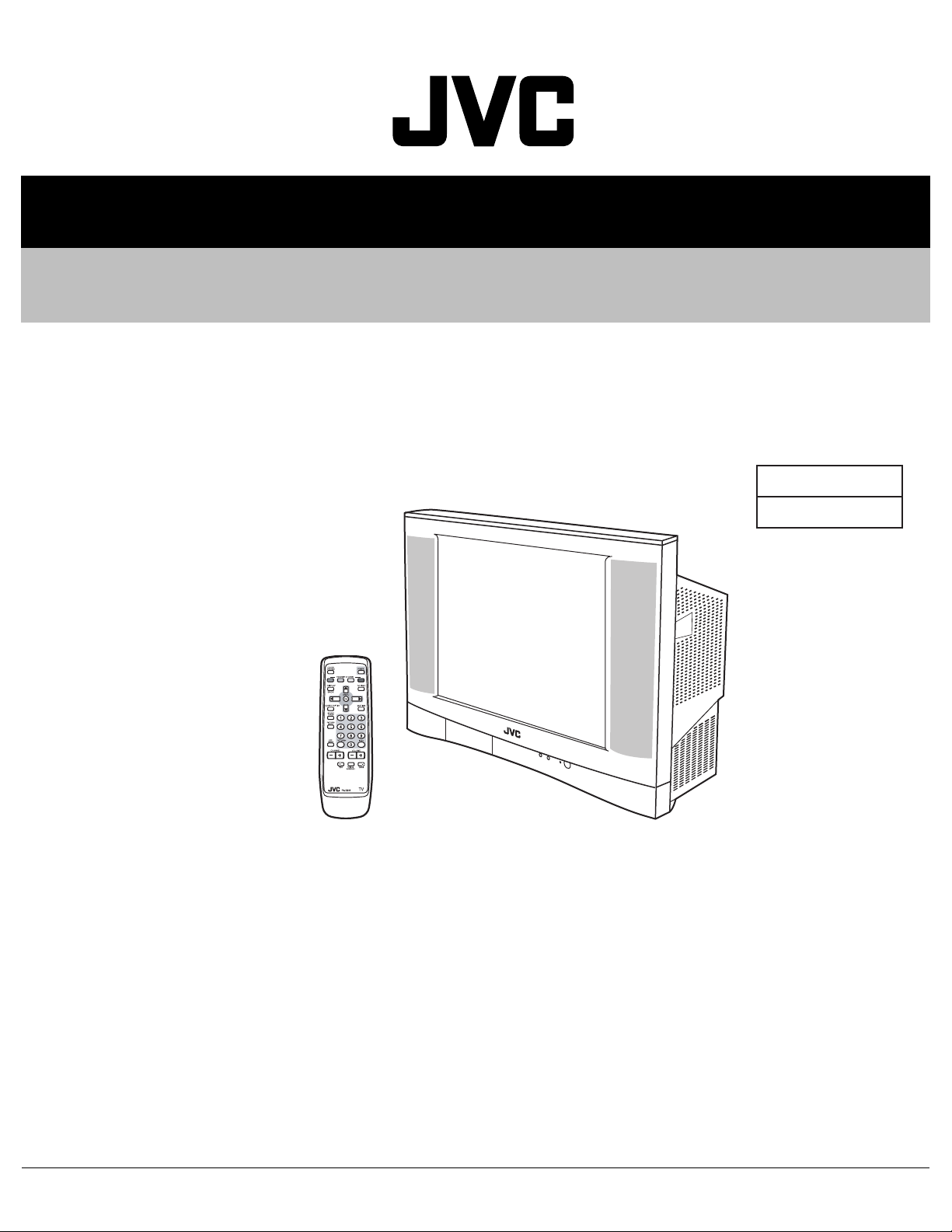
AV-29VT15/R,
AV-29VT35
/R
BASIC CHASSIS
CW
TABLE OF CONTENTS
1 PRECAUTION. . . . . . . . . . . . . . . . . . . . . . . . . . . . . . . . . . . . . . . . . . . . . . . . . . . . . . . . . . . . . . . . . . . . . . . . . 1-3
2 SPECIFIC SERVICE INSTRUCTIONS . . . . . . . . . . . . . . . . . . . . . . . . . . . . . . . . . . . . . . . . . . . . . . . . . . . . . . 1-4
3 DISASSEMBLY . . . . . . . . . . . . . . . . . . . . . . . . . . . . . . . . . . . . . . . . . . . . . . . . . . . . . . . . . . . . . . . . . . . . . . . 1-8
4 ADJUSTMENT . . . . . . . . . . . . . . . . . . . . . . . . . . . . . . . . . . . . . . . . . . . . . . . . . . . . . . . . . . . . . . . . . . . . . . . 1-14
5 TROUBLESHOOTING . . . . . . . . . . . . . . . . . . . . . . . . . . . . . . . . . . . . . . . . . . . . . . . . . . . . . . . . . . . . . . . . . 1-32
COPYRIGHT © 2005 Victor Company of Japan, Limited
No.YA256
2005/4
Page 2
SPECIFICATION
Items
Dimensions (W × H × D) 81.2cm × 58.42cm × 52.05cm
Mass 41kg 43.4kg
TV RF System M / N
Color System TV Mode
Video Mode
Stereo System MTS (Multi-Channel Television Sound)
Receiving Frequency VHF Low
VHF High
Intermediate
Frequency
Color Sub Carrier Frequency 3.58MHz (NTSC)
Aerial Input Terminal 75Ω unbalanced, coaxial
Power Input AC110V-AC240V, 50Hz / 60Hz (Operating Voltage 90V ~ 260V)
Power Consumption 166W (Max.) / 109W (Avg.) 215W (Max.) / 130W (Avg.)
Picture Tube A68QCU770X52TD
Screen Size Visible size :67.6cm (Diagonal) / 55.4cm × 41.4cm (H × V)
High Voltage 32kV -1.5kV / +1.0kV (at zero beam current)
Speaker 6.5cm × 13cm, Oval type × 26.5cm × 13cm, oval type × 2
Audio Output 10W + 10W 7W + 7W + 13W
Video / Audio Input
[1/2/3]
Video / Audio Output Video
Headphone 3.5mm stereo mini jack × 1
Remote Control Unit RM-C1288-1H
S-Video [1] Mini-DIN 4 pin × 1
Video [1/2/3] 1V(p-p), negative sync, 75Ω, RCA pin jack × 3
Audio [1/2/3] 500mV(rms) (-4dBs ), high impedance, RCA pin jack × 6
Component
Video [2]
NTSC / PAL-M / PAL-N
NTSC / PAL-M / PAL-N
46.25 MHz ~ 140.25 MHz (AS0 ~ S6)
147.25 MHz ~ 423.25 MHz (S7 ~ S36)
UHF
431.25 MHz ~ 863.25 MHz (S37 ~ C57)
CATV
Mid : X ~ Z, S1 ~ S10
Super: S11 ~ S20
Hyper: S21 ~ S41
VIF 38.0MHz
SIF 33.5MHz (4.5MHz)
29-inch, aspect ratio 4:3, flat square face type, tinted
Y: 1V(p-p), positive (negative sync provided), 75Ω
C: 0.286V(p-p) (Burst signal), 75Ω
RCA pin jack × 3
Y:1V(p-p), positive (negative sync), 75Ω
Cb/Cr:0.7V(p-p), 75Ω
1V(p-p), 75Ω, RCA pin jack × 1
Audio
500mV(rms)(-4dBs), Low impedance (400Hz when modulated 100%), RCA pin jack × 2
(AA/R06/UM-3 battery × 2)
AV-29VT15/R AV-29VT35/R
Contents
13cm, round type × 1 (Bass blaster unit)
Design & specifications are subject to change without notice.
1-2 (No.YA256)
Page 3

SECTION 1
PRECAUTION
1.1 SAFETY PRECAUTIONS
(1) The design of this product contains special hardware,
many circuits and components specially for safety
purposes. For continued protection, no changes should be
made to the original design unless authorized in writing by
the manufacturer. Replacement parts must be identical to
those used in the original circuits. Service should be
performed by qualified personnel only.
(2) Alterations of the design or circuitry of the products should
not be made. Any design alterations or additions will void
the manufacturer's warranty and will further relieve the
manufacturer of responsibility for personal injury or
property damage resulting therefrom.
(3) Many electrical and mechanical parts in the products have
special safety-related characteristics. These
characteristics are often not evident from visual inspection
nor can the protection afforded by them necessarily be
obtained by using replacement components rated for
higher voltage, wattage, etc. Replacement parts which
have these special safety characteristics are identified in
the parts list of Service manual. Electrical components
having such features are identified by shading on the
schematics and by ( ) on the parts list in Service
manual. The use of a substitute replacement which does
not have the same safety characteristics as the
recommended replacement part shown in the parts list of
Service manual may cause shock, fire, or other hazards.
(4) Don't short between the LIVE side ground and
ISOLATED (NEUTRAL) side ground or EARTH side
ground when repairing.
Some model's power circuit is partly different in the GND.
The difference of the GND is shown by the LIVE : ( ) side
GND, the ISOLATED (NEUTRAL) : ( ) side GND and
EARTH : ( ) side GND.
Don't short between the LIVE side GND and ISOLATED
(NEUTRAL) side GND or EARTH side GND and never
measure the LIVE side GND and ISOLATED (NEUTRAL)
side GND or EARTH side GND at the same time with a
measuring apparatus (oscilloscope etc.). If above note will
not be kept, a fuse or any parts will be broken.
(5) If any repair has been made to the chassis, it is
recommended that the B1 setting should be checked or
adjusted (See B1 POWER SUPPLY check).
(6) The high voltage applied to the picture tube must conform
with that specified in Service manual. Excessive high
voltage can cause an increase in X-Ray emission, arcing
and possible component damage, therefore operation
under excessive high voltage conditions should be kept to
a minimum, or should be prevented. If severe arcing
occurs, remove the AC power immediately and determine
the cause by visual inspection (incorrect installation,
cracked or melted high voltage harness, poor soldering,
etc.). To maintain the proper minimum level of soft X-Ray
emission, components in the high voltage circuitry
including the picture tube must be the exact replacements
or alternatives approved by the manufacturer of the
complete product.
(7) Do not check high voltage by drawing an arc. Use a high
voltage meter or a high voltage probe with a VTVM.
Discharge the picture tube before attempting meter
connection, by connecting a clip lead to the ground frame
and connecting the other end of the lead through a 10kΩ
2W resistor to the anode button.
(8) When service is required, observe the original lead dress.
Extra precaution should be given to assure correct lead
dress in the high voltage circuit area. Where a short circuit
has occurred, those components that indicate evidence of
overheating should be replaced. Always use the
manufacturer's replacement components.
(9) Isolation Check (Safety for Electrical Shock Hazard)
After re-assembling the product, always perform an
isolation check on the exposed metal parts of the cabinet
(antenna terminals, video/audio input and output terminals,
Control knobs, metal cabinet, screw heads, earphone jack,
control shafts, etc.) to be sure the product is safe to operate
without danger of electrical shock.
a) Dielectric Strength Test
The isolation between the AC primary circuit and all metal
parts exposed to the user, particularly any exposed metal
part having a return path to the chassis should withstand a
voltage of 3000V AC (r.m.s.) for a period of one second. (.
. . . Withstand a voltage of 1100V AC (r.m.s.) to an
appliance rated up to 120V, and 3000V AC (r.m.s.) to an
appliance rated 200V or more, for a period of one second.)
This method of test requires a test equipment not generally
found in the service trade.
b) Leakage Current Check
Plug the AC line cord directly into the AC outlet (do not use
a line isolation transformer during this check.). Using a
"Leakage Current Tester", measure the leakage current
from each exposed metal part of the cabinet, particularly
any exposed metal part having a return path to the chassis,
to a known good earth ground (water pipe, etc.). Any
leakage current must not exceed 0.5mA AC (r.m.s.).
However, in tropical area, this must not exceed 0.2mA AC
(r.m.s.).
Alternate Check Method
Plug the AC line cord directly into the AC outlet (do not
use a line isolation transformer during this check.). Use
an AC voltmeter having 1000Ω per volt or more
sensitivity in the following manner. Connect a 1500Ω
10W resistor paralleled by a 0.15µF AC-type capacitor
between an exposed metal part and a known good earth
ground (water pipe, etc.). Measure the AC voltage
across the resistor with the AC voltmeter. Move the
resistor connection to each exposed metal part,
particularly any exposed metal part having a return path
to the chassis, and measure the AC voltage across the
resistor. Now, reverse the plug in the AC outlet and
repeat each measurement. Any voltage measured must
not exceed 0.75V AC (r.m.s.). This corresponds to
0.5mA AC (r.m.s.).
However, in tropical area, this must not exceed 0.3V AC
(r.m.s.). This corresponds to 0.2mA AC (r.m.s.).
AC VOLTMETER
(HAVING 1000 /V,
OR MORE SENSITIVITY)
0.15 F AC-TYPE
PLACE THIS PROBE
1500 10W
GOOD EARTH GROUND
ON EACH EXPOSED
ME TAL PAR T
(No.YA256)1-3
Page 4
SECTION 2
SPECIFIC SERVICE INSTRUCTIONS
2.1 FEATURES
• New chassis design enables use of an interactive on-screen control.
• Pure flat CRT produces fine textured picture in every detail.
• Wide range voltage (110V ~ 240V) for AC power input.
• With AUDIO/VIDEO/S-VIDEO/COMPONENT input terminals.
2
C bus control utilizes single chip ICs.
•I
• By means of AUTO PROGRAM, the TV stations can be selected automatically and the TV channels can also be rearranged
automatically.
• Built-in DIGITAL ECO MODE (ECONOMY, ECOLOGY).
In accordance with the brightness in a room, the brightness and/or contrast of the picture can be adjusted automatically to make the
optimum picture which is easy on the eye.
• Built-in OFF TIMER & RETURN +.
2.2 MAIN DIFFERENCE LIST
Items AV-29VT15/R AV-29VT35/R
BASS BLASTER None BASS BLASTER UNIT
AUDIO OUTPUT 10W + 10W 7W + 7W + 13W
POWER CONSUMPTION 166W (Max.) / 109W (Avg.) 215W (Max.) / 130W (Avg.)
1-4 (No.YA256)
Page 5
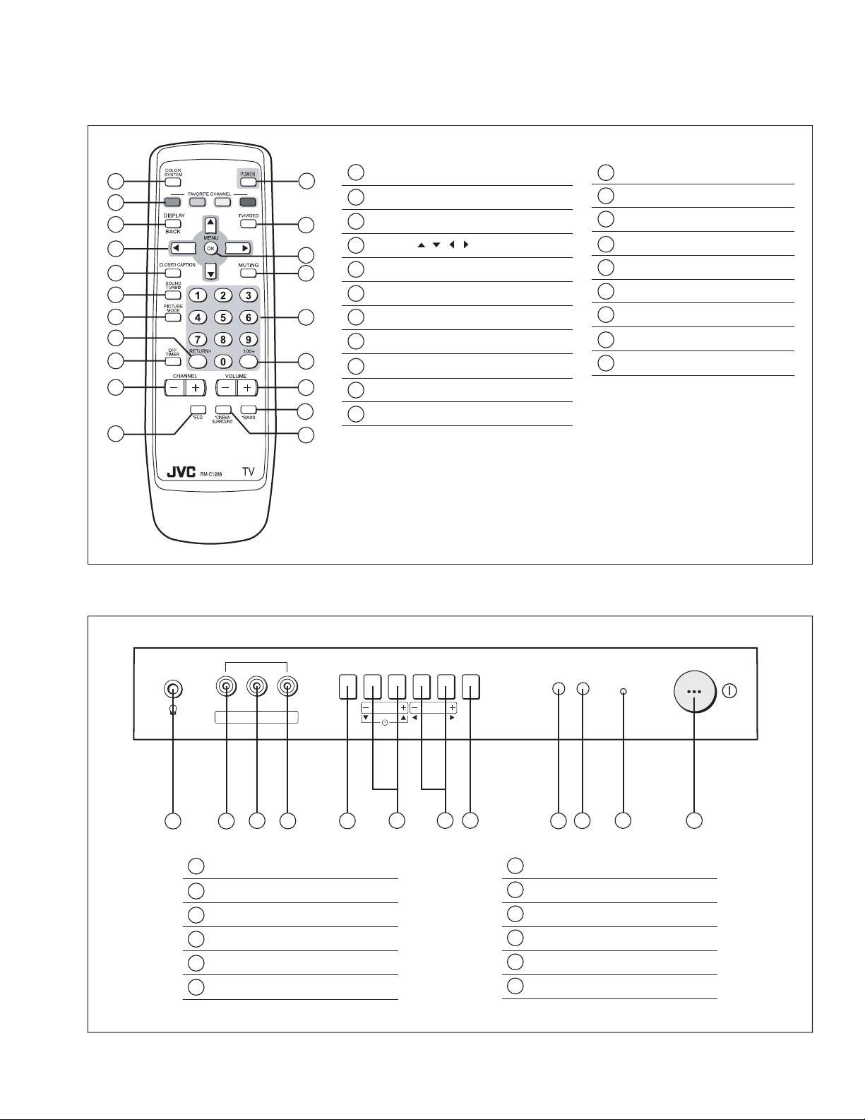
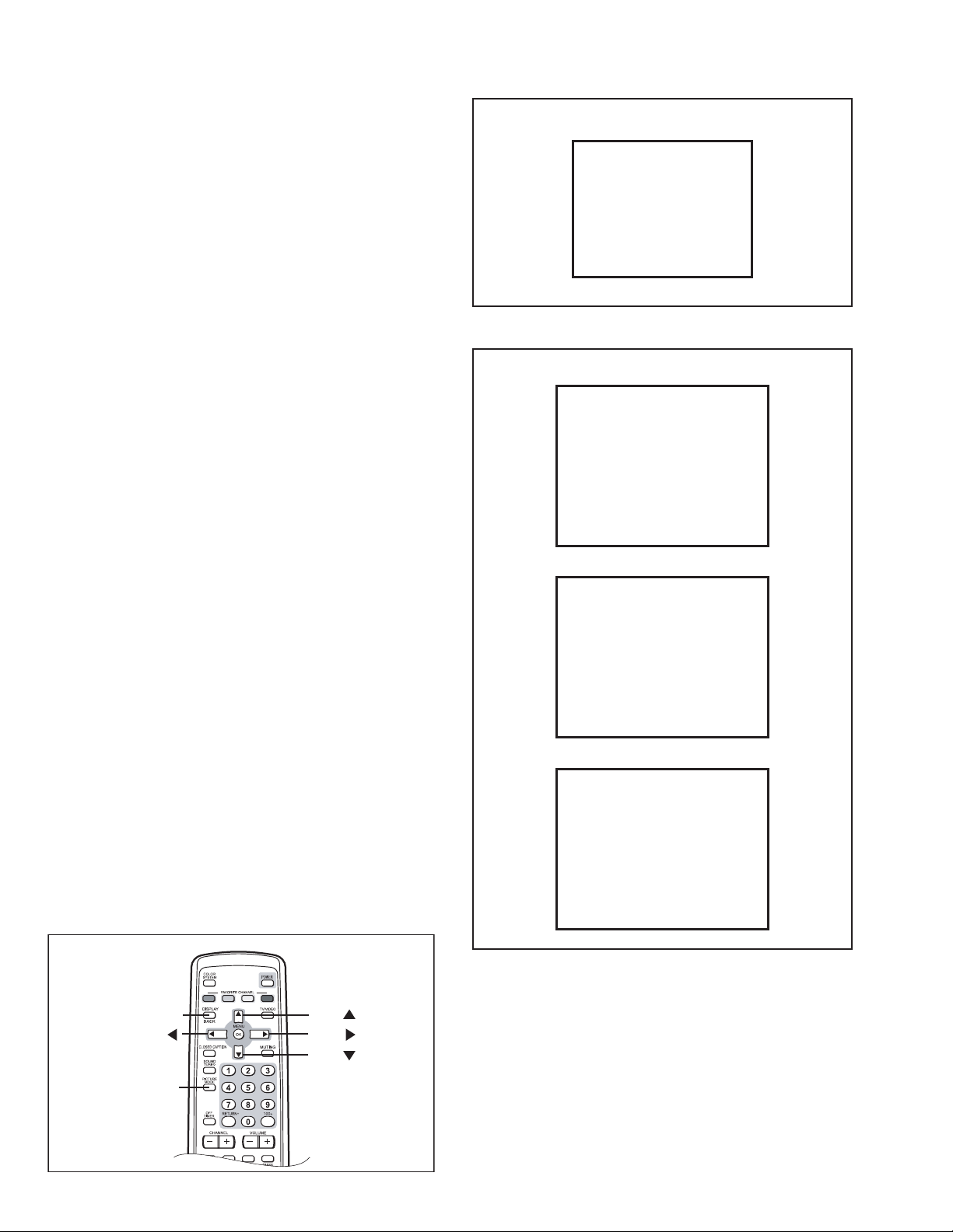
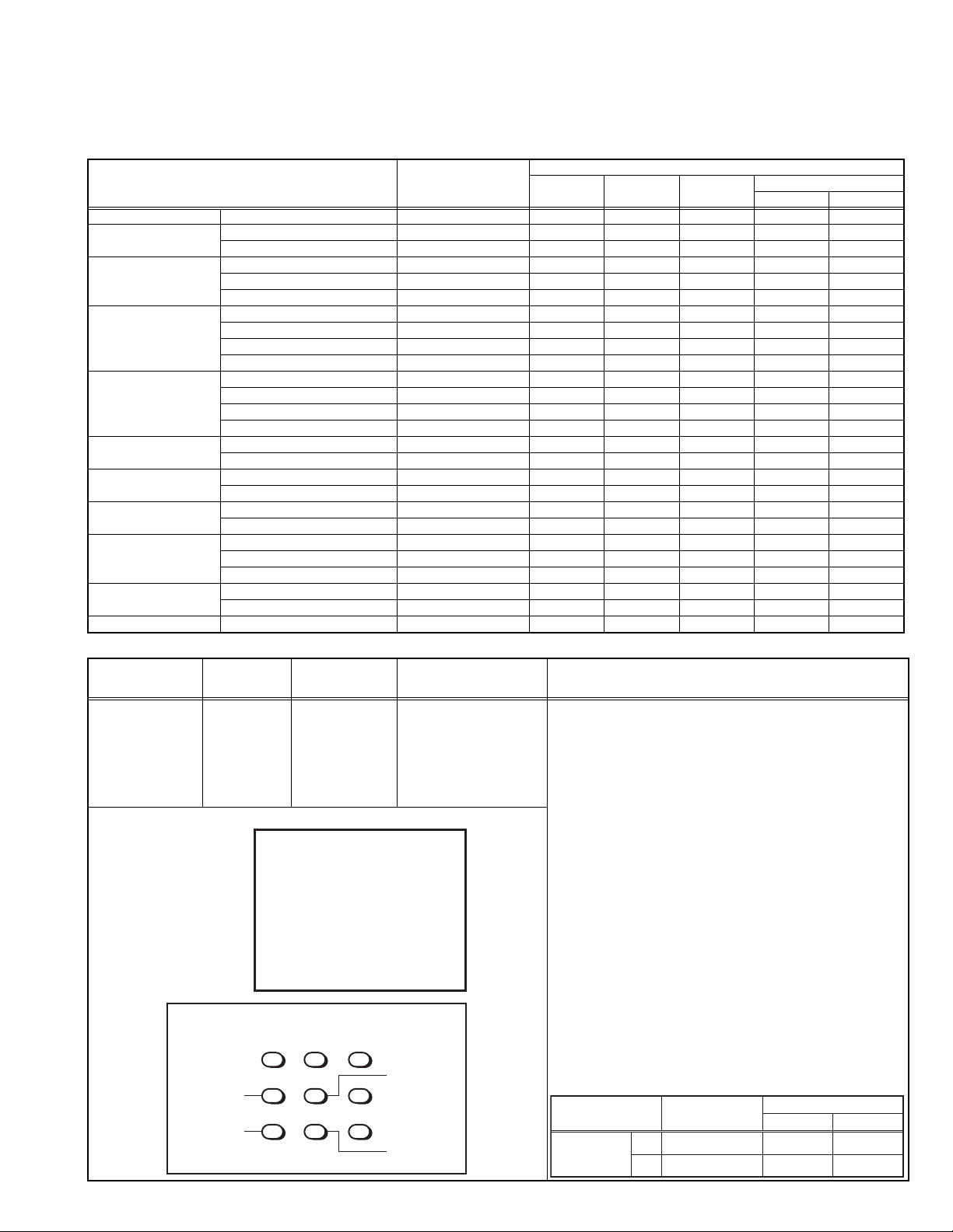
2.3 FUNCTIONS
REMOTE CONTROL UNIT
RM-C1288-1H
10
11
COLOR SYSTEM key
1
12
2
3
4
5
13
14
15
6
7
16
8
9
17
18
19
1
FAVORITE CHANNEL keys
2
DISPLAY BACK key
3
MENU ( / , / ) keys
4
CLOSED CAPTION key
5
SOUND TURBO key
6
7
PICTURE MODE key
8
RETURN + key
9
OFF TIMER key
CHANNEL (-/+) keys
10
ECO key
11
POWER key
12
TV / VIDEO key
13
14
MENU (OK) key
MUTING key
15
16
Number keys
17
100+ key
18
VOLUME (-/+) keys
19
BASS key [AV-29VT35/R]
20
CINEMA SURROUND key
20
FRONT PANEL CONTROLS
L/MONO
VR
IN (VIDEO-3)
1
2
HEADPHONE jack
1
IN (VIDEO-3) : VIDEO
2
IN (VIDEO-3) : AUDIO L/MONO
3
IN (VIDEO-3) : AUDIO R
4
MENU (OK) button
5
CHANNEL (-/+) buttons
6
10
POWER
11 12
CHANNEL
MENU
OK
3
4
5
VOLUME
6 7
TV/VIDEO
EXIT
8
9
7
VOLUME (-/+) buttons
8
TV/VIDEO EXIT buttons
9
Remote control sensor
10
ECO sensor
11
POWER lamp
12
MAIN POWER button
(No.YA256)1-5
Page 6
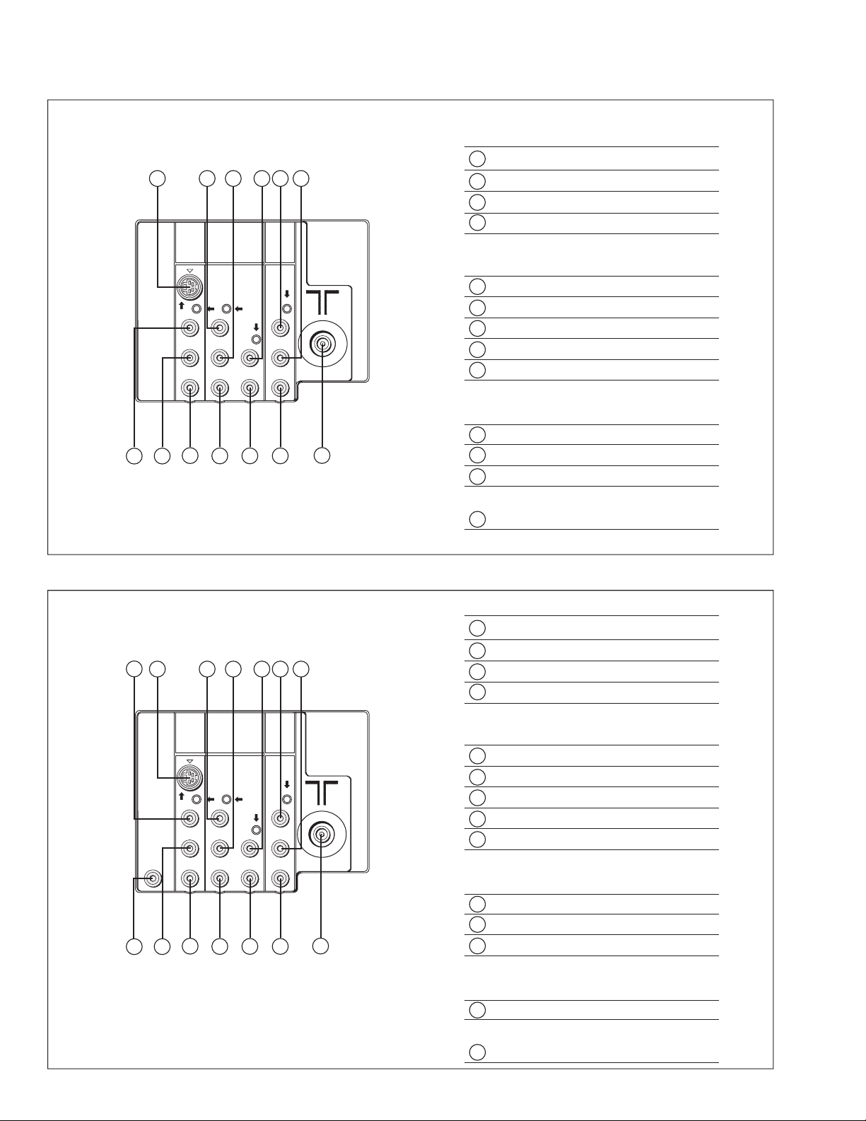
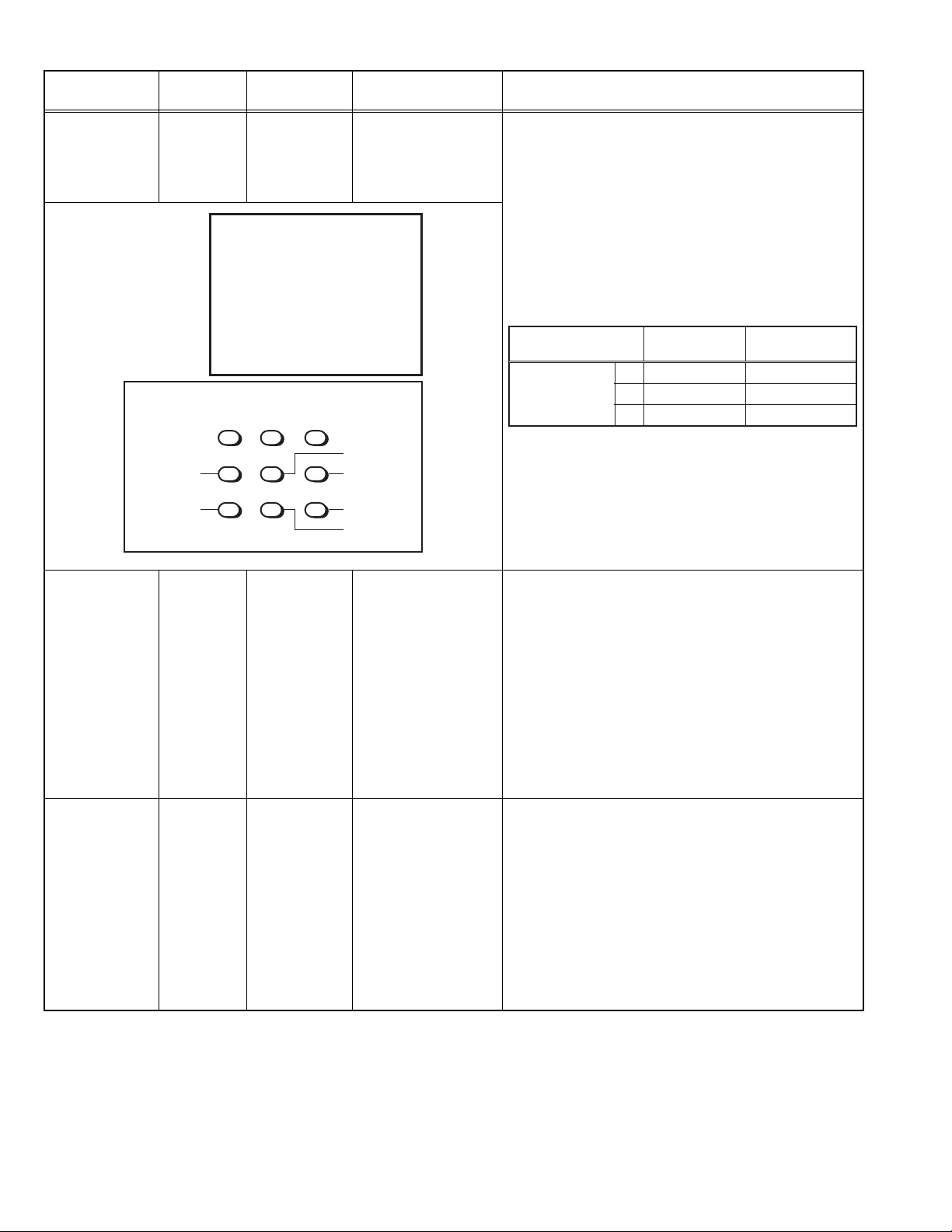
REAR TERMINAL
[AV-29VT15/R]
2
1
3
VIDEO-1
INPUT
S
OVER
V
L
/
MONO
R
4
5 6 10 118
COMPONENT
(VIDEO-2)
INPUT
Y
/
V
L
B
C
/
MONO
C
R
9
7
OUTPUT
V
L
RR
12
13
VIDEO-1 INPUT TERMINAL
S-VIDEO
1
VIDEO
2
AUDIO L/MONO
3
AUDIO R
4
COMPONENT (VIDEO-2) INPUT TERMINAL
Y/VIDEO
5
6
B
C
C
R
7
8
AUDIO L/MONO
9
AUDIO R
OUTPUT TERMINAL
VIDEO
10
11
AUDIO L
12
AUDIO R
[AV-29VT35/R]
2
BASS
SPEAKER
13
1
OUT
3
VIDEO-1
INPUT
S
OVER
V
L
/
MONO
R
4
5 6 10 118
COMPONENT
(VIDEO-2)
INPUT
Y
/
V
L
B
C
/
MONO
C
R
9
7
OUTPUT
V
L
RR
12
14
13
Aerial input terminal
VIDEO-1 INPUT TERMINAL
S-VIDEO
1
VIDEO
2
AUDIO L/MONO
3
AUDIO R
4
COMPONENT (VIDEO-2) INPUT TERMINAL
Y/VIDEO
5
6
C
B
C
R
7
8
AUDIO L/MONO
9
AUDIO R
OUTPUT TERMINAL
VIDEO
10
11
AUDIO L
12
AUDIO R
1-6 (No.YA256)
BASS BLASTER UNIT OUTPUT TERMINAL
13
BASS SPEAKER OUT
14
Aerial input terminal
Page 7
2.4 MAIN CPU [MAIN PWB : IC701] PIN FUNCTION
Pin no. Pin name I/O Remark
1VssP2 -GND
2 VssC4 - GND
3 V1.8C4 I 1.8V (Digital)
4 V3.3A3 I 3.3V
5 VrefP_Sdac I 3.3V (Positive)
6 VrefN_Sdac - GND
7 VrefP_Sdac I 3.3V (Negative)
8 VrefN_Sdac - GND
9 VrefP_Sdac I 3.3V (Positive)
10 XtalIn I 24.567MHz for system clock
11 XtalOut O 24.567MHz for system clock
12 VssA1 - GND
13 NECK I V-guard input/ I/O switch
14 CONT I 1.8V regulator control
15 V5P1 I +5V
16 Ph2 - Phase-2 filter
17 Ph1 - Phase-1 filter
18 Gnd1 - GND
19 SecPll - SECAM PLL decoupling
20 Dec8G - Bandgap decoupling
21 EW O East-West drive output
22 VDRB- O Vertical drive B output
23 VDRA+ O Vertical drive A output
24 Vif1 I Video IF input 1
25 Vif2 I Video IF input 2
26 Vsc - Vertical sawtooth capacitor
27 Iref I Reference current input
28 GndIF - GND
29 Sif1 I Sound IF input 1
30 Sif2 I Sound IF input 2
31 AGC O Tuner AGC output
32 EHT I EHT/overvoltage protection input
33 Ssif/RefIn/Avl/RefOut O
34 L3 I Audio-L3 input (left signal)
35 R3 I Audio-R3 input (right signal)
36 L_OUT O Audio L output
37 R_OUT O Audio R output
38 DecsDem - Decoupling sound demodulator
39 QssO/AmO/AudeEm O QSS intercarrier output / AM output /
40 Gnd2 - GND
41 PllIf - IF-PLL loop filter
42 SifAgc - AGC sound IF
43 IfVo/FmRo/DvbO O Not used
44 NC O Not used
45 V8AudioSwitches I 8V
46 AgcSsif - AGC capacitor second sound IF
47 V5P2 I 5V
48 V_OUT O Video output
49 L1 I Audio-L1 input
50 R1 I Audio-R1 input
51 V3 I Video V3 input
52 C4 I Not used
53 Audio2InL I Not used
54 Audio2InR I Not used
55 V2/Y I Video 2 input
56 L2 I Audio L2 input (Left signal)
57 R2 I Audio R2 input (right signal)
58 Y3/Cvbs I S-Video Y1 input
59 C1 I S-Video C1 input
60 AudioLsL O Audio L output for audio power amplifier
61 AudioLsR O Audio R output for audio power amplifier
62 HP_L O Headphone L
63 HP_R O Headphone R
Automatic Volume Levelling/ sound IF input /
subcarrier reference output / external reference
signal input for I signal mixer for DVB operation
deemphasis / (front-end audio out)
Pin no. Pin name I/O Remark
64 CVBSO/PIP O CVBS / PIP output
65 SVM O Scan velocity modulation output
66 FbiSo I Flyback input/sandcastle output
67 Hout O Horizontal output
68 VssComb - GND
69 V5Comb I 5V
70 Vin/R2/Pr I PIP R input
71 Uin/B2/Pb I PIP B input
72 Yin/G2/Y I PIP G input
73 Ysync I Not used
74 Yout O Not used
75 Uout/INSSW2 I YUV insertion input
76 NC O Not used
77 INSSW3 I YUV insertion input
78 R3/Pr I Component PR input (Video-2)
79 G3/Y I Component Y input (Video-2)
80 B3/Pb I Component PB input (Video-2)
81 Gnd3 - GND
82 V5P3 I 5V
83 BCL I Beam current limiter input
84 BLKIN I Black current input
85 Rout O R output
86 Gout O G output
87 Bout O B output
88 V3.3A1 I 3.3V
89 RefAdN - GND
90 V3.3RefAdP I 3.3V (Positive)
91 RefAd I 3.3/2V
92 GndA - GND
93 V1.8A I 1.8V
94 V3.3A2 I 3.3V
95 VssADC - GND
96 V1.8ADC I 1.8V
97 REMOTE I Remote control
98 PW_LED I POWER LED control
99 P11/TO I POWER LED control
100 V1.8C2 I 1.8V
101 VssC2 - GND
102 COMPONENT-PIP - Not used
103
COMB_SW_NT3.5/OTHER
104 VER_PROTECT O X-ray protect
105 S_REDUCE O Sound control
106 P00/I2SDI1 O Not used
107 POWER O SUB POWER control
108 SCL1 I I2C bus clock
109 SDA1 I/O I2C bus clock
110 V3.3P I 3.3V
111 ROTATION O ROTATION
112 3.58/OTHER O
113 A_MUTE O Audio muting
114 4.5/OTHER O NTSC 4.43 detection
115 PROT I Protect
116 ECO_IN I ECO sensor level detection
117 V1.8C1 I 1.8V (Digital)
118 DecV1V8 I 1.8V
119 KEY_IN I Key scan data
120 VDO_DET I Video DET input
121 VSSC1+P1 - Digital GND
122 P24/PWM3 I S-Video DET input
123 P25/PWM4 O GTVA_reset
124 V1.8C3 I 1.8V (Digital)
125 VssC3 - GND
126 P12/Int2 I External interrupt
127 SDA0 I/O I2C bus data (for memory)
128 SCL0 I I2C bus clock (for memory)
- Not used
NTSC 3.58 detection
(No.YA256)1-7
Page 8

SECTION 3
DISASSEMBLY
3.1 DISASSEMBLY PROCEDURE
3.1.1 REMOVING THE TWIN PORT BASS BLASTER UNIT
[AV-29VT35/R]
• Unplug the power supply cord.
(1) Disconnect the TWIN PORT BASS BLASTER UNIT's cord
from the rear of the TV set.
(2) Remove the TWIN PORT BASS BLASTER UNIT by pulling
it upwards.
NOTE:
After removing the TWIN PORT BASS BLASTER UNIT,
proceed to the following procedure.
3.1.2 REMOVING THE REAR COVER
• Unplug the power cord.
(1) Remove the 16 screws [A] as shown in Fig.1.
(2) Withdraw the REAR COVER toward you.
CAUTION:
When reinstalling the rear cover, carefully push it inward after
inserting the MAIN PWB into the REAR COVER groove.
3.1.3 REMOVING THE CHASSIS (CHASSIS BASE AND
CONTROL BASE)
• Remove the REAR COVER.
(1) Slightly raise the both sides of the CHASSIS by hand and
remove the 2 claws [B] under the CHASSIS from the front
cabinet as shown in Fig.1.
(2) Withdraw the CHASSIS backward.
(If necessary, take off the wire clamp, connectors etc.)
NOTE:
When conducting a check with power supplied, be sure to
confirm that the CRT earth wire is connected to the CRT
SOCKET PWB and the MAIN PWB.
3.1.6 REMOVING THE SPEAKER
• Remove the REAR COVER.
(1) Remove the 2 screws [G] as shown in Fig.1.
(2) Withdraw the SPEAKER backward.
(3) Follow the same steps when removing the other hand
SPEAKER.
3.1.7 CHECKING THE MAIN PW BOARD
• To check the back side of the MAIN PWB.
(1) Pull out the CHASSIS and CONTROL BASE. (Refer to the
procedure described in REMOVING THE CHASSIS)
(2) Put the CHASSIS in upright position with the MAIN PWB's
solderside faced to the right. The FBT must be positioned
on top. (Viewed from the rear)
(3) Put the CONTROL PWBs in an appropriate position, taking
care not giving tension to the ribbon cables that connect to
the MAIN PWB.
CAUTIONS:
• Use insulating materials, if necessary, to avoid possible
electrical contacts between PWBs and expose terminals,
etc.
• Before turning on power, make sure that the CRT earth wire
and other connectors are properly connected.
• When repairing, connect the DEG. COIL to the DEG.
connector on the MAIN PWB.
3.1.8 WIRE CLAMPING AND CABLE TYING
(1) Be sure to clamp the wire.
(2) Never remove the cable tie used for tying the wires
together.
Should it be inadvertently removed, be sure to tie the wires
with a new cable tie.
3.1.4 REMOVING THE AV TERMINAL BOARD
• Remove the REAR COVER.
(1) Remove the 4 screws [C] as shown in Fig.1.
(2) When you pull out the AV TERMINAL BOARD in the
direction of arrow [D] as shown in Fig.1, it can be removed.
3.1.5 REMOVING THE CONTROL BASE
• Remove the REAR COVER.
• Remove the CHASSIS.
(1) While pushing down the 2 claws [E] as shown in Fig. 2 and
pull out the CONTROL BASE in the direction of arrow [F]
as shown in Fig. 2, the control base can be removed.
(If necessary, take off the wire, connectors etc.)
1-8 (No.YA256)
Page 9
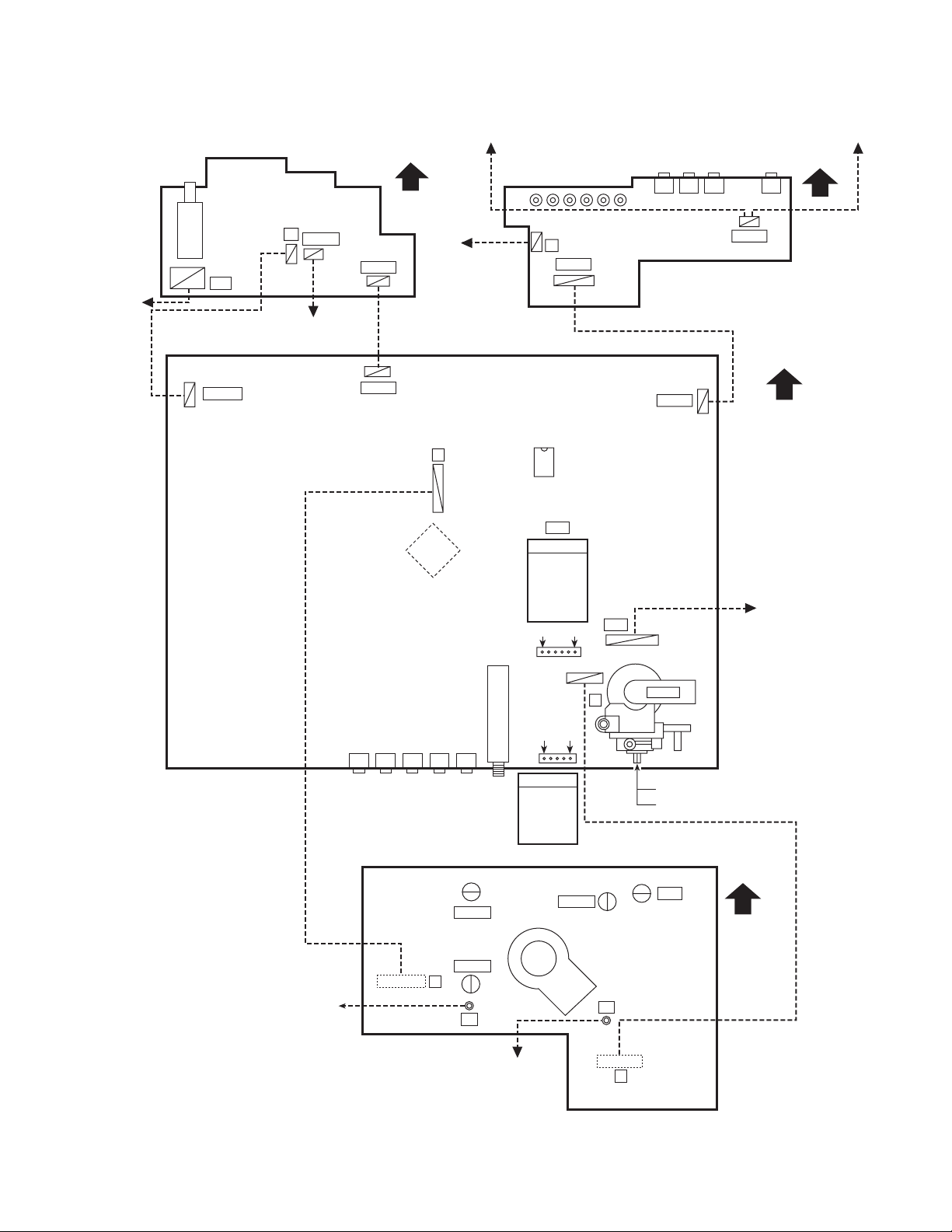
FRONT CABINET
PICTURE TUBE
SPEAKER
(X2)
[FRONT SIDE]
CONTROL BASE
E
G
F
CHASSIS
BASE
Fig.2
SPEAKER
G
REAR COVER
FRONT CONTROL
PWB (1/2)
(X2)
CONTROL BASE
CRT
SOCKET PWB
CHASSIS
BASE
CLAW B
(under side)
BASS SPEAKER OUT JACK
[AV-29VT35/R]
Fig.2
FRONT CONTROL PWB (2/2)
CLAW B
(under side)
MAIN PWB
FBT
AV TERMINAL
BOARD
D
C
(×4)
Fig.1
A
(×16)
TWIN PORT
BASS BLASTER UNIT
[AV-29VT35/R]
(No.YA256)1-9
Page 10
3.2 REPLACEMENT OF MEMORY IC
3.2.1 MEMORY IC
This TV uses the following memory IC.
Memory IC: IC702 on MAIN PWB
The memory IC memorizes data for correctly operating the video
and deflection circuits. When replacing the memory IC, be sure
to use the same type IC written with the initial values of data. In
other words, use the specific IC listed in "PRINTED WIRING
BOARD PARTS LIST". For its mounting location, refer to
"ADJUSTMENT LOCATIONS".
3.2.2 PROCEDURE FOR REPLACING MEMORY IC
1. Power off
Switch the power off and unplug the power cord from the wall
outlet.
2. Replacing the memory IC
Replace the memory IC with new one. Be sure to use the
memory IC written with the initial data values.
3. Power on
Plug the power cord into the wall outlet and switch the power on.
4. Check and setting of SYSTEM CONSTANT SET:
(1) Press the [DISPLAY] key and the [PICTURE MODE] key
on the remote control unit simultaneously.
The SERVICE MENU screen will be displayed.(See
Fig.1.)
(2) In the SERVICE MENU, press the [DISPLAY] key and
[PICTURE MODE] key simultaneously. Then, the
SYSTEM CONSTANT SET screen will be
displayed.(See Fig.2.)
(3) Check whether the setting values of the SYSTEM
CONSTANT SET are the same as those indicated in
Table 1.
If the value is different, select the setting item with the
MENU [] / [] key, and set the correct value with the
MENU [] / [] key.
(4) Press the [DISPLAY] key twice to return to the normal
screen.
5. Receive channel setting
Refer to the OPERATING INSTRUCTIONS and set the
receive channels (channels preset).
6. User setting
Check the user setting values in Table 2 and Table 3. If setting
value is different, set the correct value.
For setting, refer to the OPERATING INSTRUCTIONS.
7. Setting of SERVICE MENU
Verify the setting for each setting item in the SERVICE
MENU.(See Table 4.) If readjustment is necessary, perform
adjustment referring to "ADJUSTMENTS PROCEDURE".
NAME OF REMOTE CONTROL KEYS
SERVICE MENU
SERVICE MENU
1. IF
3. AUDIO
5. VSM W/B
7. PLUG & PLAY (ON)
1-7 : SELECT DISPLAY : EXIT
******* **** ***** *****
**** **** *** ***
2. V/C
4. DEF
6. S TATUS
Fig.1
SYSTEM CONSTANT-1
SYSTEM CONSTANT
SYSTEM OTHERS
COMB
TILT
SUPER BASS
: SEL : OPE
SET 1
YES
YES
NO
DISP : EXIT
SYSTEM CONSTANT-2
SYSTEM CONSTANT SET 2
SOUND
BLUE BACK MUTE
ECO SENSOR
: SEL : OPE
STEREO
NO
YES
DISP : EXIT
SYSTEM CONSTANT-3
SYSTEM CONSTANT SET 3
SURROUND
: SEL : OPE
YES
NOPICTURE BOOSTER
YESCOMPONENT
YESS INPUT
DISP : EXIT
Fig.2
DISPLAY / BACK
PICTURE
MODE
1-10 (No.YA256)
MENU
MENU
MENU
MENU
Page 11
3.2.3 FACTORY SETTING VALUE
SETTING OF SYSTEM CONSTANT SET
Setting item Setting content
SYSTEM OTHERS
COMB YES
TILT YES
SUPER BASS YES
SOUND STEREO
BLUE BACK MUTE NO
ECO SENSOR YES
SURROUND YES
PICTURE BOOSTER NO
COMPONENT YES
S INPUT YES
TAIWAN OTHERS
YES NO
YES NO
YES NO
STEREO PB MONO
YES NO
YES NO
YES NO
YES NO
YES NO
YES NO
AV-29VT15/R AV-29VT35/R
Setting
NO
value
Table 1
(No.YA256)1-11
Page 12
SETTING OF BASIC FUNCTIONS
Setting item Setting value
POWER Off
SUB POWER On
VOLUME 15
COLOR SYSTEM PAL-N
PICTURE MODE (VSM) BRIGHT
CINEMA SURROUND OFF
SUPER BASS ON [AV-29VT35/R]
OFF TIMER OFF
CLOSED CAPTION OFF
CHANNEL POSITION CH02
Table 2
SETTING OF MENU SCREEN
Setting item Setting value
INPUT TV
VNR AUTO
COMPRESS (16:9) OFF
PICTURE TILT
AUTO SHUTOFF OFF
CHILD LOCK OFF
BLUE BACK ON
VIDEO-2 SET VIDEO
AUTO PROGRAM
CHANNEL SUMMARY
WHITE BALANCE COOL
TINT Center
COLOR Center
BRIGHT Center
PICTURE Maximum
DETAIL Center
BALANCE Center
SOUND MODE DYNAMIC
SOUND TURBO OFF
AI VOLUME ON
MTS STEREO
FAVORITE CH RED CH02
FAVORITE CH GREEN CH03
FAVORITE CH YELLOW CH04
FAVORITE CH BLUE CH05
AI ECO SENSOR OFF
AI ECO DISPLAY ON
Refer to OPERATING INSTRUCTIONS
Refer to OPERATING INSTRUCTIONS
SERVICE MENU SETTING ITEMS
Setting item Setting value
1. IF 1. VCO
2. DELAY POINT
2. V/C 1. SCREEN
2. CUTOFF(B/G)
3. WDR(R/G/B)
4. BRIGHT(TV/VDO 1/2/3)
5. CONT(TV/VDO 1/2/3/TV 16:9/VDO 16:9)
6. COLOR(TV/VDO1/2/3/DVD)
7. TINT(TV/VDO 1/2/3)
8. SHARP [Do not adjust]
9. Y DELAY [Do not adjust]
10. TINT DVD [Do not adjust]
11. AMP T. SHARP
3. AUDIO
[Do not adjust]
4. DEF 1. V-SHIFT
5. VSM W/B
(BRIGHT/STANDARD/SOFT)
(COOL/WARM/NORMAL)
6. STATUS
[Display only]
7. PLUG & PLAY(ON)
[Display only]
1. DCXO ADJ
2. NICAM lower ERRLIM
3. NICAM upper ERRLIM
4. A2 ID THR
5. MENU EQUALIZER
2. V-SLOPE
3. V-SIZE
4. H-CENT
5. H-SIZE
6. TRAPEZ
7. EW-PIN
8. COR-UP
9. COR-LO
10. ANGLE
11. BOW
12. V-S.CR
13. V-LIN
14. V-ZOOM
15. V-SCROLL
1. BRIGHT
2. CONT
3. COLOR
4. SHARP
5. HUE
1. R DRIVE
2. G DRIVE
3. B DRIVE
Table 4
1-12 (No.YA256)
Table 3
Page 13
3.3 REPLACEMENT OF CHIP COMPONENT
3.3.1 CAUTIONS
(1) Avoid heating for more than 3 seconds.
(2) Do not rub the electrodes and the resist parts of the pattern.
(3) When removing a chip part, melt the solder adequately.
(4) Do not reuse a chip part after removing it.
3.3.2 SOLDERING IRON
(1) Use a high insulation soldering iron with a thin pointed end of it.
(2) A 30w soldering iron is recommended for easily removing parts.
3.3.3 REPLACEMENT STEPS
1. How to remove Chip parts
2. How to install Chip parts
[Resistors, capacitors, etc.]
(1) As shown in the figure, push the part with tweezers and
alternately melt the solder at each end.
(2) Shift with the tweezers and remove the chip part.
[Transistors, diodes, variable resistors, etc.]
(1) Apply extra solder to each lead.
SOLDER
SOLDER
[Resistors, capacitors, etc.]
(1) Apply solder to the pattern as indicated in the figure.
(2) Grasp the chip part with tweezers and place it on the
solder. Then heat and melt the solder at both ends of the
chip part.
[Transistors, diodes, variable resistors, etc.]
(1) Apply solder to the pattern as indicated in the figure.
(2) Grasp the chip part with tweezers and place it on the
solder.
(3) First solder lead A as indicated in the figure.
(2) As shown in the figure, push the part with tweezers and
alternately melt the solder at each lead. Shift and remove
the chip part.
NOTE :
After removing the part, remove remaining solder from the
pattern.
A
B
C
(4) Then solder leads B and C.
A
B
C
(No.YA256)1-13
Page 14
SECTION 4
ADJUSTMENT
4.1 ADJUSTMENT PREPARATION
(1) You can make the necessary adjustments for this unit with either the remote control unit or with the adjustment
equipment and parts as given below.
(2) Adjustment with the remote control unit is made on the basis of the initial setting values, however, the new setting
values used for setting the screen to its optimum condition may differ from the initial settings.
(3) Make sure that AC power is turned on correctly.
(4) Turn on the power for the set and test equipment before use, and start the adjustment procedures after waiting at least 30
minutes.
(5) Unless otherwise specified, prepare the most suitable reception or input signal for adjustment.
(6) Never touch any adjustment parts, which are not specified in the list for this variable resistors, transformers, trimmer capacitors,
etc.
4.2 PRESETTING BEFORE ADJUSTMENT
Unless otherwise specified in the adjustment instructions, preset the following functions with the remote control unit.
User mode setting position
Setting item Setting value
PICTURE MODE (VSM) BRIGHT
TINT, COLOR, BRIGHT,DETAIL Center
PICTURE Maximum
VNR OFF
AI ECO SENSOR OFF
BALANCE Center
SOUND TURBO OFF
CINEMA SURROUND OFF
COMPRESS 4:3
4.3 MEASURING INSTRUMENT AND FIXTURES
(1) DC voltmeter (or Digital voltmeter)
(2) Oscilloscope
(3) Signal generator (Pattern generator) [PAL/SECAM/NTSC]
(4) Remote control unit
4.4 ADJUSTMENT ITEMS
B1 VOLTAGE
FOCUS ADJUSTMENT
IF CIRCUIT ADJUSTMENTS
• IF VCO adjustment
• DELAY POINT (AGC TAKE-OVER) adjustment
VIDEO CIRCUIT ADJUSTMENTS
• WHITE BALANCE (Low light) adjustment
• WHITE BALANCE (High light) adjustment
• SUB BRIGHT adjustment
• SUB CONTRAST adjustment
• SUB COLOR 1 adjustment
• SUB COLOR 2 adjustment
• SUB TINT 1 adjustment
• SUB TINT 2 adjustment
AUDIO SETTING
DEFLECTION CIRCUIT ADJUSTMENTS
• V.SLOPE adjustment
• V.POSITION adjustment
• V.HEIGHT adjustment
• H.POSITION adjustment
• H. WIDTH adjustment
• SIDE PIN adjustment
• TRAPEZIUM adjustment
• V.S-CURVE adjustment
• CORNER adjustment
• H. PARALLEL adjustment
• H.BOW adjustment
VSM PRESET SETTING
CONVERGENCE ADJUSTMENTS
• STATIC CONVERGENCE adjustment
• DYNAMIC CONVERGENCE adjustment
1-14 (No.YA256)
Page 15
4.5 ADJUSTMENT LOCATIONS
FRONT CONTROL PWB ASS’Y (1/2) FRONT CONTROL PWB ASS’Y (2/2)
POWER
CORD
S901
PW
MAIN PWB ASS’Y
CN00W
W
CNDEG
DEG COIL
CN001
CN001
FRONT
ROTATION COIL
T
IC701
SPEAKER (L)
1
8
S805
S804
R
IC702
I2C
CN00C
1. 5V
2. SCL0
3. SDA0
4. SCL1
5. SDA1
6. GND
GND 5V
S806 S802
CN002
16
S803S801
HV
J804 J803 J802
CN002
16
CN00S
FRONT
J801
FRONT
DEF YOKE
SPEAKER (R)
CRT EARTH
(BRAIDED ASS'Y)
J804J801J805 J802 J803
TU001
CRT SOCKET PWB ASS’Y
TP-47R
TP-47G
18
T
E2
CRT EARTH
(BRAIDED ASS'Y)
GND B1
CN00X
1. B1
2. NC
3. X-RAY2
4. X-RAY1
5. GND
61
U
15
TP-47B
E1
16
HVT
UPPER : FOCUS
LOWER : SCREEN
(SOLDER SIDE)
TOP
TP-E
U
(No.YA256)1-15
Page 16
4.6 BASIC OPERATION IN SERVICE MENU
Operate the SERVICE MENU with the remote control unit.
4.6.1 SERVICE MENU ITEMS
With the SERVICE MENU, various settings (adjustments) can be made, and they are broadly classified in the following items of settings:
1. IF For entering/adjusting the setting values (adjustment values) of the IF circuit.
2. V/C For entering/adjusting the setting values (adjustment values) of the VIDEO circuit.
3. AUDIO For entering/adjusting the setting values (adjustment values) of the AUDIO circuit.
4. DEF For entering/adjusting the setting values (adjustment values) of the DEFLECTION circuit.
5. VSM W/B For setting the values of STANDARD, SOFT, BRIGHT and COOL, NORMAL, WARM.
6. STATUS This is not used for service.
7. PLUG & PLAY (ON) This is not used for service.
4.6.2 BASIC OPERATION IN SERVICE MENU
1. HOW TO ENTER SERVICE MENU
Press the [DISPLAY] key and the [PICTURE MODE] key on the remote control unit simultaneously.
The SERVICE MENU screen will be displayed. (See Fig. 1 on the next page.)
2. SELECTION OF SUB MENU SCREEN
Press one of the keys 1 to 6 on the remote control unit, and select the SUB MENU SCREEN from the SERVICE MENU. (See Fig.1 on the next page.)
SERVICE MENU → SUB MENU
1. IF 5. VSM W/B
2. V/C 6. STATUS
3. AUDIO 7. PLUG & PLAY (ON)
4. DEF
3. METHOD OF SETTING
NOTES:
• Once the setting values are set, they are memorized automatically.
• It must not be adjusted without inputting a signal.
(1) 1. IF
[1.VCO ] : Under normal conditions, no adjustment is required.
(a) [1] key Select 1. IF.
(b) [1] key Select 1. VCO.
(c) [DISPLAY] key When this is pressed twice, you will return to the SERVICE MENU.
[2.DELAY POINT ]
(a) [1] key Select 1. IF.
(b) [2] key Select 2. DELAY POINT.
(c) MENU [] / [] key Adjust the setting value.
(d) [DISPLAY] key When this is pressed twice, you will return to the SERVICE MENU.
(2) 2. V/C, 3. AUDIO and 4. DEF
(a) [2] ~[4] keys Select one from 2. V/C, 3. AUDIO and 4. DEF
(b) MENU [] / [] key Select setting items.
(c) MENU [] / [] key Adjust the setting values of the setting items.
Use the number keys on the remote control unit for setting the WHITE BALANCE.
For the setting, refer to each item concerned.
(d) [DISPLAY] key When this is pressed, you will return to the SERVICE MENU.
(3) 5. VSM W/B
(a) [5] keys Select 5. VSM W/B.
(b) MENU [OK] key Select preset items.
(c) MENU [] / [] key Adjust setting items.
(d) MENU [] / [] key Adjust the setting values of the setting items.
(e) [DISPLAY] key When this is pressed, you will return to the SERVICE MENU.
(4) 6. STATUS
This is for display only.
(5) 7. PLUG & PLAY (ON)
This is not used for service.
4. Release of SERVICE MENU
After completing the setting, return to the SERVICE MENU by pressing the [DISPLAY] key, then again press the [DISPLAY] key to
return to the normal screen.
1-16 (No.YA256)
Page 17
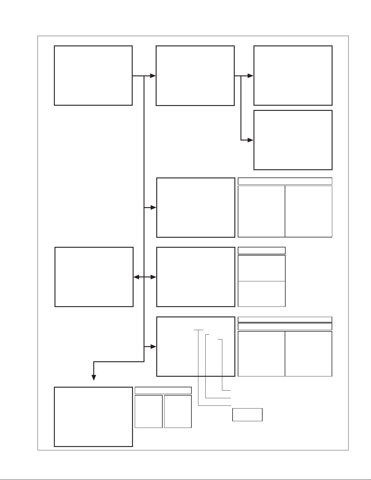
4.6.3 SERVICE MENU FLOW CHART
SERVICE MENU
SERVICE MENU
1. IF
3. AUDIO
5. VSM W/B
7. PLUG & PLAY (ON)
1-7 : SELECT DISPLAY : EXIT
******* **** ***** *****
**** **** *** ***
2. V/C
4. DEF
6. STATUS
IF SERVICE MENU
1. VCO
2. DELAY POINT
V/C
1. SCREEN
1. IF
2. V/C
PAL
HBC
WBC
BRI
VCO (CW)
TOO HIGH
ABOVE REFERENCE
JUST REFERENCE
BELOW REFERENCE
TOO LOW
DELAY POINT
AGC TAKEOVER
Setting item
1. SCREEN
2. CUTOFF (B/G)
**
**
**
3. WDR (R/G/B)
4. BRIGHT (TV/VDO1/2/3)
5. CONT (TV/VDO1/2/3/TV
16:9/VDO16:9)
6. COLOUR (TV/VDO1/2/3/
DVD)
7. TINT (TV/VDO1/2/3)
8. SHARP (TV/VDO1/2/3)
Y DELAY (TV/VDO1/2/3
9.
/S-VDO)
10. TINT DVD
11. AMP T.SHARP
*****
**
MHz
6. STATUS
STATUS
V/C STATUS
ECO EOF NOL VNR
***********
COSMIC STATUS
** ** ** ** ** ** ** **
5. VSM W/B
VSM PRESET BRIGHT
1. BRIGHT
***
1. BRIGHT
2. CONT
3. COLOUR
4. SHARP
5.HUE
Setting item
1. R-DRIVE
2. G-DRIVE
3. B-DRIVE
3. AUDIO
AUDIO
1. DCXO ADJ. =
NOT NICAM
0002
0009
000A
***
*******
*******
*******
4. DEF
DEF FULL 50Hz
1. V-SHIFT
***
(**)
Setting item
1. DCXO ADJ
2. NICAM lower ERRLIM
3. NICAM upper ERRLIM
4. A2 ID THR
MENU EQUALIZER
DYNAMIC
MUSIC
NEWS
USER
4 : 3 / 16 : 9
Setting item
1. V-SHIFT
2. V-SLOPE
3. V-SIZE
4. H-CENT
5. H-SIZE
6. TRAPEZ
7. EW-PIN
8. COR-UP
Setting value (Hexadecimal)
Setting value
Sereen size
FULL
COMPRESS
9. COR-LO
10. ANGLE
11. BOW
12. V-S. CR
13. V-LIN
14. V-ZOOM
15. V-SCROLL
Fig.1
(No.YA256)1-17
Page 18
4.7 ADJUSTMENT PROCEDURE
4.7.1 B1 VOLTAGE
Item
B1 VOLTAGE
check
Measuring
instrument
Signal
generator
B1 (pin 1)
GND (pin 5)
[CN00X
DC voltmeter
connector in
MAIN PWB]
4.7.2 FOCUS ADJUSTMENT
Item
FOCUS
adjustment
Measuring
instrument
Signal
generator
Test point Adjustment part Description
(1) Receive a black and white signal.
(2) Connect a DC voltmeter between B1 and GND
(between pins 1 and 5 of the connector CN00X).
(3) Make sure that the voltage is DC134.5V ± 2V.
Test point Adjustment part Description
FOCUS VR
[In HVT]
Notes:
• Set PICTURE MODE (VSM) to "BRIGHT".
• The final adjustment of CONVERGENCE must be
done after the FOCUS adjustment. (CONVERGENCE
is affected by the FOCUS adjustment.)
If any aeviation in CONVERGENCE is found, PURITY
must be adjusted to restore the convergence.
(1) Receive a crosshatch signal.
(2) Adjust the FOCUS VR so that the vertical and
horizontal lines will be clear and in fine detail on the
screen.
(3) Make sure that the picture is in focus even when the
screen gets darkened.
4.7.3 IF CIRCUIT ADJUSTMENTS
Item
IF VCO
check
DELAY POINT
(AGC
Measuring
instrument
Remote
control unit
VCO (CW)
TOO HIGH
ABOVE REFERENCE
JUST REFERENCE
BELOW REFERENCE
TOO LOW
DISPLAY : EXIT
Remote
control unit
. MHz
TAKE-OVER)
adjustment
Adjustment item
NTSC 3.58
VHF UHF
2. DELAY POINT
(AGC TAKE-OVER)
28
Test point Adjustment part Description
[1. IF]
1. VCO (CW)
Note:
• Under normal conditions, no adjustment is required.
(1) Receive a broadcast signal.
Receiving frequency
(2) Select 1. IF from the SERVICE MENU.
(3) Select 1. VCO.
(4) Check the characters color of the JUST
REFERENCE displayed to yellow.
YELLOW
(5) Press the [DISPLAY] key three times to return to
normal screen.
[1. IF]
2. DELAY POINT
(1) Receive a black and white broadcast signal (color off).
(2) Select 1. IF from the SERVICE MENU.
(3) Select 2. DELAY POINT.
(4) Adjust in order to eliminate any noise or beat from
the image. Any increase above the initial value
Initial setting value
OTHERS
VHF UHF
produces the noise and any decrease below it
produces the beat.
(5) Press the [DISPLAY] key three times to return to the
normal screen.
28
28
28
(6) Turn to other channels and make sure that there are
no irregularities.
1-18 (No.YA256)
Page 19
4.7.4 VIDEO CIRCUIT ADJUSTMENTS
• The setting (adjustment) using the remote control unit is made on the basis of the initial setting values.
• The setting values which adjust the screen to the optimum condition can be different from the initial setting values.
• Do not change the initial setting values of the setting (adjustment) items not listed in "ADJUSTMENT PROCEDURE".
• The initial setting values in parenthesis ( ) are fixed offset values, needing no further adjustment.
Initial setting value
Adjustment item Variable range
1. SCREEN BRI 0 ~ 63 32 32 32 32 32
2. CUTOFF B 0 ~ 63 (-32 ~ +31) 11 11 11 (-3) (-3)
G 0 ~ 63 (-32 ~ +31) 7 7 7 (-5) (-5)
3. WDR R 0 ~ 63 (-32 ~ +31) 32 32 32 (0) (0)
G 0 ~ 63 (-32 ~ +31) 32 32 32 (0) (0)
B 0 ~ 63 (-32 ~ +31) 45 45 45 (0) (0)
4. BRIGHT RF 0 ~ 63 (-32 ~ +31) 39 39 39 --- --VIDEO 1(COMPOSITE/S) (-32 ~ +31) (+1) (+1) (+1) --- --VIDEO 2(COMPONENT) (-32 ~ +31) (+1) (+1) (+1) (+3) (+3)
VIDEO 3(COMPOSITE) (-32 ~ +31) (+2) (+2) (+2) --- ---
5. CONT. RF 0 ~ 63 32 32 32 --- --VIDEO (-32 ~ +31) (+2) (+2) (+2) (+2) (+2)
RF 16:9 (-32 ~ +31) (0) (0) (0) --- --VIDEO 16:9 (-32 ~ +31) --- --- --- --- ---
6. COLOR RF 0 ~ 63 (-32 ~ +31) 42 32 37 --- --VIDEO 0 ~ 63 (-32 ~ +31) (+1) (+4) (-3) (+7) (+2)
7. TINT RF 0 ~ 63 (-32 ~ +31) --- --- 27 --- --VIDEO (-32 ~ +31) --- --- (+1) --- ---
8. SHARP RF 0 ~ 63 28 28 28 --- --VIDEO 0 ~ 63 40 40 40 15 15
9. Y DELAY RF 0 ~ 15 11 11 14 --- --VIDEO 0 ~ 15 997-----S-VIDEO 0 ~ 15 9 10 11 --- ---
10. TINT DVD VIDEO, S-VIDEO 0 ~ 63 34 36 32 --- --COMPONENT (-32 ~ +31) --- --- --- (0) (-2)
11. AMP T.SHARPRF, VIDEO 0 ~ 63 00000
PAL SECAM
NTSC3.58
COMPONENT (V-2)
525i 625i
Item
WHITE
BALANCE
(Low light)
adjustment
Measuring
instrument
Signal
generator
Remote
control unit
B CUTOFF (
B CUTOFF (
Test point Adjustment part Description
V/C
2. CUTOFF
REMOTE CONTROL UNIT
12 3
4
)
789
)
PAL
(B)
(G)
56
[2. V/C]
2. CUTOFF (B)
2. CUTOFF (G)
SCREEN VR
[In HVT]
(**)
**
)
(
**
**
G CUTOFF ( )
G CUTOFF (
)
Note:
• Set PICTURE MODE (VSM) to "BRIGHT".
- COMPOSITE WHITE BALANCE -
(1) Receive a PAL black and white signal (color off).
(2) Select 2. V/C from the SERVICE MENU.
(3) Select 2. CUTOFF (B) and (G).
(4) Set each value to initial setting value with the [4] /
[7] keys and [5] / [8] keys.
(5) Turn the SCREEN VR fully counterclockwise, then
slowly turn it clockwise to where a red, blue or
green color is faintly visible.
(6) Use the [4] / [7] and [5] / [8] keys to adjust so that
the other 2 colors appear white.
(7) Turn the SCREEN VR to where the single
horizontal line glows faintly.
(8) Press the [DISPLAY] key twice to return to the
normal screen.
- COMPONENT WHITE BALANCE -
(1) Receive a PAL component black and white signal
(color off).
(2) Select VIDEO-2 SET from the MENU and set
VIDEO-2 SET to COMPONENT.
(3) Adjust COMPONENT WHITE BALANCE in the
same way as ”COMPOSITE WHITE BALANCE”.
Adjustment Item
2. CUT OFF
B 0 ~ 63(-32~+31)
G (-5)
Variable
range
0 ~ 63(-32~+31)
Initial setting value
COMPOSITE COMPONENT
11
7
(-3)
(No.YA256)1-19
Page 20
Item
WHITE
BALANCE
(High light)
adjustment
Measuring
instrument
Signal
generator
Remote
control unit
Test point Adjustment part Description
[2. V/C]
3. WDR (R)
3. WDR (G)
3. WDR (B)
Notes:
• Proceed to the following adjustment after having
completed the WHITE BALANCE (Low light) adjustment.
• Set PICTURE MODE (VSM) to "BRIGHT".
(1) Receive a PAL black and white signal (color off).
(2) Select 2. V/C from the SERVICE MENU.
(3) Select 3. WDR (R), (G) and (B).
V/C
3. WDR
PAL
(R)
(G)
(B)
(**)
**
(
**
**(**
)
**
)
(4) Set each value to initial setting value with the [4] to
[9] keys.
(5) Use the [4] to [9] keys to produce a white screen.
(6) Press the [DISPLAY] key twice to return to the normal
screen.
SUB BRIGHT
adjustment
SUB
CONTRAST
adjustment
REMOTE CONTROL UNIT
12 3
4
R DRIVE (
) B DRIVE ()
R DRIVE (
)
56
789
Remote
control unit
Remote
control unit
G DRIVE ()
B DRIVE (
)
G DRIVE (
)
[2. V/C]
4. BRIGHT
[2. V/C]
5. CONT
Adjustment Item
3. WDR G 32
Variable Initial setting
range value
R32
0 ~ 63
0 ~ 63
B45
0 ~ 63
Notes:
• Proceed to the following adjustment after having
completed the WHITE BALANCE (Low light) and
WHITE BALANCE (High light) adjustment.
• Set PICTURE MODE (VSM) to "BRIGHT".
(1) Receive a broadcast.
(2) Select 2. V/C from the SERVICE MENU.
(3) Select 4. BRIGHT.
(4) Set the initial setting value.
(5) If the brightness is not best with the initial setting value,
make fine adjustment until you get the best brightness.
(6) Press the [DISPLAY] key twice to return to the
normal screen.
Notes:
• Proceed to the following adjustment after having
completed the SUB BRIGHT adjustment.
• Set PICTURE MODE (VSM) to "BRIGHT".
(1) Receive a broadcast.
(2) Select 2. V/C from the SERVICE MENU.
(3) Select 5. CONT.
(4) Set the initial setting value.
(5) If the contrast is not best with the initial setting value,
make fine adjustment until you get the best contrast.
(6) Press the [DISPLAY] key twice to return to the
normal screen.
1-20 (No.YA256)
Page 21

Item
SUB COLOR 1
adjustment
Measuring
instrument
Remote
control unit
Test point Adjustment part Description
[2. V/C]
6. COLOUR
[Method of adjustment without measuring instrument]
Notes:
• Proceed to the following adjustment after having
completed the SUB CONTRAST adjustment.
• Set PICTURE MODE (VSM) to "BRIGHT".
- PAL-M COLOR -
(1) Receive a PAL-M broadcast.
(2) Select 2. V/C from the SERVICE MENU.
(3) Select 6. COLOUR.
(4) Set the initial setting value for PAL-M COLOR.
(5) If the color is not best with the initial setting value,
adjust until you get the best color.
(6) Press the [DISPLAY] key twice to return to the
normal screen.
- PAL-N COLOR -
(1) Receive a PAL-N broadcast.
(2) Press the [COLOR SYSTEM] key to select the PAL-
N color system.
(3) Adjust PAL-N COLOR in the same way as for "PAL-
M COLOR".
- SECAM COLOR -
(1) Receive a SECAM broadcast.
(2) Press the [COLOR SYSTEM] key to select the
SECAM color system.
(3) Adjust SECAM COLOR in the same way as for
"PAL-M COLOR".
- NTSC 3.58 COLOR -
(1) Receive a NTSC 3.58MHz broadcast.
(2) Press the [COLOR SYSTEM] key to select the
NTSC 3.58 color system.
(3) Adjust NTSC 3.58 COLOR in the same way as for
"PAL-M COLOR".
(No.YA256)1-21
Page 22
Item
SUB COLOR 2
adjustment
SUB TINT 1
adjustment
Measuring
instrument
Signal
generator
Oscilloscope
Remote
control unit
Y
W
Signal
generator
Remote
control unit
Test point Adjustment part Description
TP-47G
TP-E
[CRT SOCKET
PWB]
[2. V/C]
6. COLOUR
[Method of adjustment using measuring instrument]
Notes:
• Proceed to the following adjustment after having
completed the SUB CONTRAST adjustment.
• Set PICTURE MODE (VSM) to "BRIGHT".
- PAL-M COLOR -
(1) Receive a PAL-M color bar signal (full field color bar
75% white).
(2) Select 2. V/C from the SERVICE MENU.
(3) Select 6. COLOUR.
B
M
R
C
G
(A)
(–)
0V
(+)
(4) Set the initial setting value of PAL-M COLOR.
(5) Connect the oscilloscope between TP-47G and TP-E.
(6) Adjust PAL-M COLOR to set the value (A) in the
figure to +10V.
- PAL-N COLOR -
(1) Receive a PAL-N color bar signal (full field color bar
75% white).
(2) Select 2. V/C from the SERVICE MENU.
(3) Select 6. COLOUR.
(4) Set the initial setting value of PAL-N COLOR.
(5) Connect the oscilloscope between TP-47G and TP-E.
(6) Adjust PAL-N COLOR to set the value (A) in the figure
to +8V.
- SECAM COLOR -
(1) Receive a SECAM color bar signal (color bar 75%
white).
(2) Press the [COLOR SYSTEM] key to select the
SECAM color system.
(3) Set the initial setting value of SECAM COLOR.
(4) Adjust SECAM COLOR to set the value (A) in the
figure to ---.
- NTSC 3.58 COLOR -
(1) Receive a NTSC 3.58 color bar signal (full field color
bar 75% white).
(2) Press the [COLOR SYSTEM] key to select the
NTSC 3.58 color system.
(3) Set the initial setting value of NTSC 3.58 COLOR.
(4) Adjust NTSC 3.58 COLOR to set the value (A) in the
figure to +6V.
[2. V/C]
7. TINT
[Method of adjustment without measuring instrument]
Notes:
• Proceed to the following adjustment after having
completed the SUB CONTRAST adjustment.
• Set PICTURE MODE (VSM) to "BRIGHT".
- NTSC 3.58 TINT -
(1) Receive a NTSC 3.58 color bar signal (full field color
bar 75% white).
(2) Press the [COLOR SYSTEM] key to select the
NTSC 3.58 color system.
(3) Select 2. V/C from the SERVICE MENU.
(4) Select 7. TINT.
(5) Set the initial setting value of NTSC 3.58.
(6) If you cannot get the best tint with the initial setting
value, make fine adjustment until you get the best
tint.
(7) Press the [DISPLAY] key twice to return to the
normal screen.
1-22 (No.YA256)
Page 23
Item
SUB TINT 2
adjustment
Measuring
instrument
Signal
generator
Oscilloscope
Remote
control unit
Test point Adjustment part Description
TP-47G
TP-E
[CRT SOCKET
PWB]
[2. V/C]
7. TINT
[Method of adjustment using measuring instrument]
Notes:
• Proceed to the following adjustment after having
completed the SUB CONTRAST adjustment.
• Set PICTURE MODE (VSM) to "BRIGHT".
- NTSC 3.58 TINT -
(1) Receive a NTSC 3.58 color bar signal (full field color
bar 75% white).
(2) Press the [COLOR SYSTEM] key to select the
NTSC 3.58 color system.
(3) Select 2. V/C from the SERVICE MENU.
(4) Select 7. TINT.
(5) Set the initial setting value of NTSC 3.58.
(6) Connect the oscilloscope between TP-47G and TP-E.
(7) Adjust NTSC 3.58 TINT to set the value (B) in the
figure to +5V.
(B)
B
M
R
C
W
G
Y
(–)
0V
(+)
(8) Press the [DISPLAY] key twice to return to the
normal screen.
4.7.5 AUDIO SETTING
This submenu is for display only, no adjustment is required.
Function Item 100Hz 300Hz 1kHz 3kHz 8kHz
MENU EQUALIZER DYNAMIC +9 +5 -2 +5 +10
MUSIC +1+2+6+5+6
NEWS -6 +1 +6 +1 -6
USER 00000
(No.YA256)1-23
Page 24
4.7.6 DEFLECTION CIRCUIT ADJUSTMENTS
• The setting (adjustment) using the remote control unit is made on the basis of the initial setting values.
• The setting values which adjust the screen to the optimum condition can be different from the initial setting values.
• When performing deflection circuit adjustment, adjusts PAL signal (fv: 50 Hz) in 4:3 mode and 16:9 mode respectively, and adjust
the NTSC signal (fv: 60 Hz) similarly.
Note:
Proceed to the following adjustment after having completed the adjustments of SUB BRIGHT and SUB PICTURE.
4. DEF
Variable range Initial setting value
Adjustment item
4:3
50Hz
Others
50Hz 60Hz 50Hz 60Hz
4:3 COMPRESS (16:9)
1. V-SHIFT 0 ~ 63 -32 ~ +31 0* 0* 0* 0*
2. V-SLOPE 0 ~ 63 -32 ~ +31 0* 0* 0* 0*
3. V-SIZE 0 ~ 63 -32 ~ +31 +15* 0* -4* -2*
4. H-CENT 0 ~ 63 -32 ~ +31 +35* 0* 0* 0*
5. H-SIZE 0 ~ 63 -32 ~ +31 +45* 0* 0* 0*
6. TRAPEZ 0 ~ 63 -32 ~ +31 0* 0* 0* 0*
7. EW-PIN 0 ~ 63 -32 ~ +31 -12* 0* 0* 0*
8. COR-UP 0 ~ 63 -32 ~ +31 0* 0* 0* 0*
9. COR-LO 0 ~ 63 -32 ~ +31 0* 0* 0* 0*
10. ANGLE 0 ~ 63 -32 ~ +31 0* 0* 0* 0*
11. BOW 0 ~ 63 -32 ~ +31 0* 0* 0* 0*
12. V-S.CR 0 ~ 63 -32 ~ +31 0* 0* 0* 0*
13. V-LIN 0 ~ 63 -32 ~ +31 0* 0* 0* 0*
14. V-ZOOM 0 ~ 63 -32 ~ +31 (+25) 0 -23* +3*
15. V-SCROLL 0 ~ 63 -32 ~ +31 (+32) (0) (0) (0)
NOTE: The value with an asterisk * is variable for adjustment. The values in parenthesis ( ) are fixed values.
COMPRESS: OFF (4:3)
Item
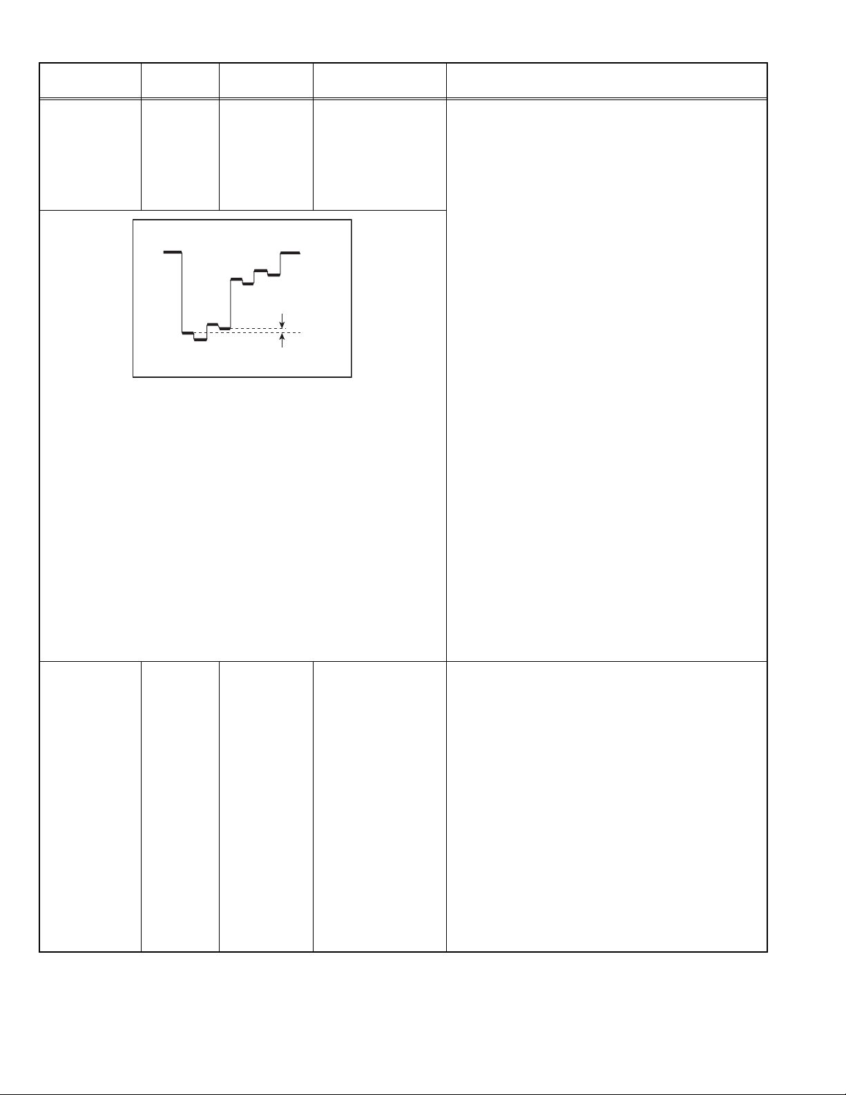
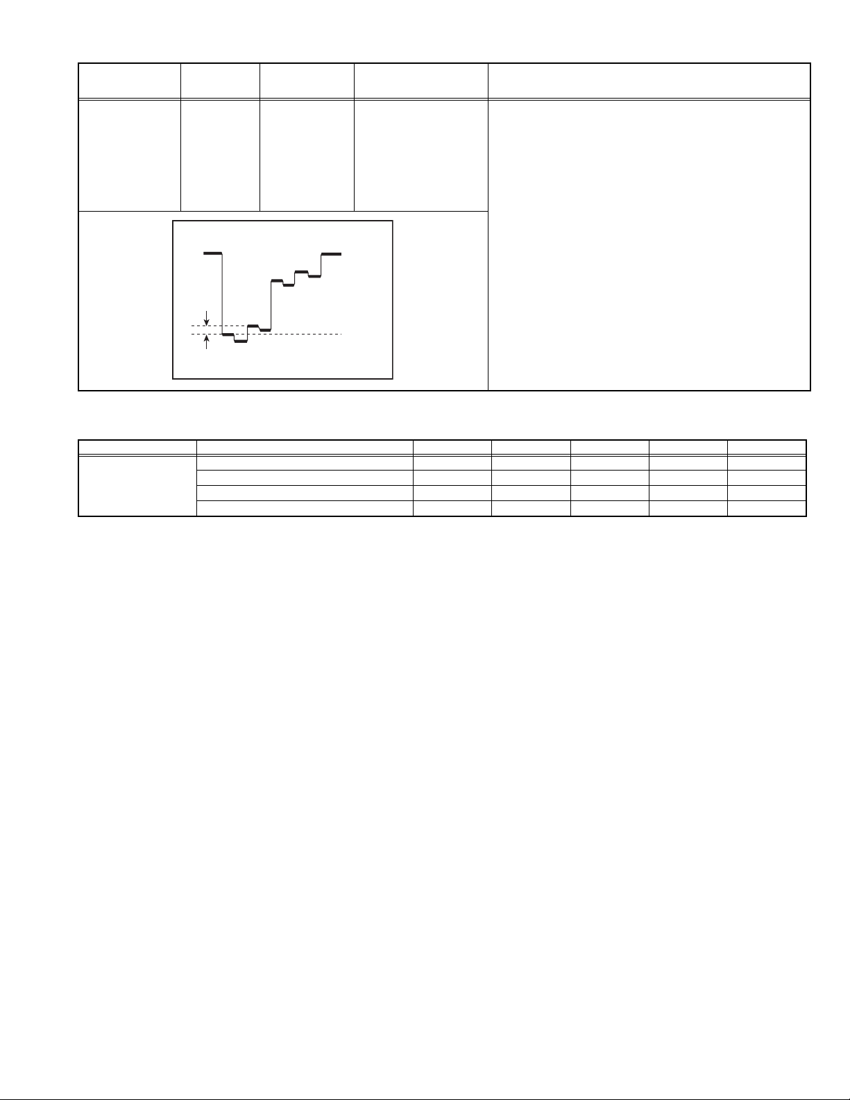
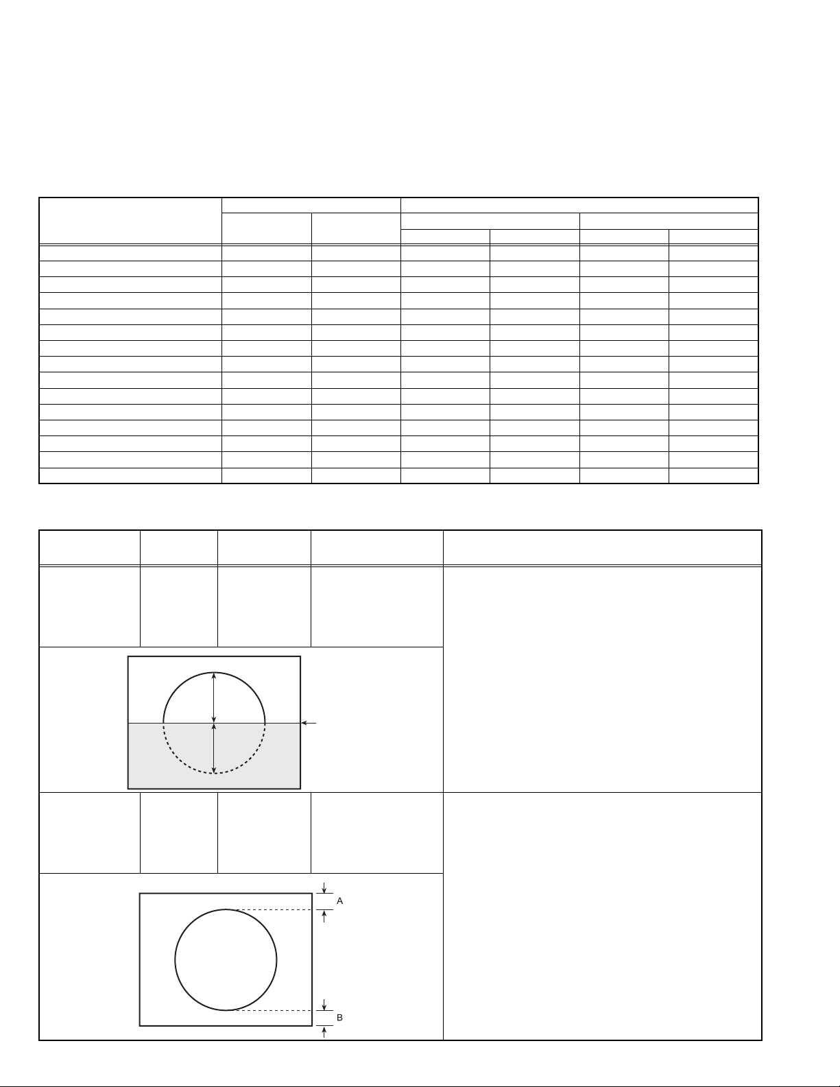
V. SLOPE
adjustment
Measuring
instrument
Signal
generator
Test point Adjustment part Description
[4. DEF]
2. V-SLOPE
- PAL V. SLOPE -
(1) Receive a PAL circle pattern signal of vertical
frequency 50Hz.
Remote
control unit
(2) Select 4. DEF from the SERVICE MENU.
(3) Select 2. V-SLOPE.
(4) Set the initial setting value of 2. V-SLOPE.
(5) Adjust 2. V-SLOPE to make "A = B".
(6) Press the [DISPLAY] key twice to return to
A
Blanking
line
B
SERVICE MENU screen.
- NTSC V. SLOPE -
(1) Receive a NTSC circle pattern signal of vertical
frequency 60Hz.
(2) Make similar adjustment of NTSC V-SLOPE in the
same way as for "PAL V-SLOPE".
V. POSITION
adjustment
1-24 (No.YA256)
Signal
generator
Remote
control unit
[4. DEF]
1. V-SHIFT
- PAL V. POSITION -
(1) Receive a PAL circle pattern signal of vertical
frequency 50Hz.
(2) Select 1. V-SHIFT.
(3) Set the initial setting value of 1. V-SHIFT.
(4) Adjust 1. V-SHIFT to make "A = B".
- NTSC V. POSITION -
(1) Receive a NTSC circle pattern signal of vertical
frequency 60Hz.
(2) Make similar adjustment of NTSC V. POSITION in
the same way as for "PAL V. POSITION".
Page 25
Item
V. HEIGHT
adjustment
Screen
size
92%
Measuring
instrument
Signal
generator
Remote
control unit
Test point Adjustment part Description
[4. DEF]
3. V-SIZE
14. V-ZOOM
- PAL V. HEIGHT -
(1) Receive a PAL crosshatch signal.
(2) Select 3. V-SIZE.
(3) Set the initial setting value of 3. V-SIZE.
(4) Select 14. V-ZOOM.
(5) Set the initial setting value of 14. V-ZOOM.
(6) Adjust 14. V-ZOOM to make the vertical screen size
to 92% of the picture size.
Picture
size
100%
- NTSC V. HEIGHT -
(1) Receive a NTSC crosshatch signal.
(2) Make similar adjustment of NTSC V. HEIGHT in the
same way as for "PAL V. HEIGHT".
H. POSITION
adjustment
H. WIDTH
adjustment
Signal
generator
[4. DEF]
4. H-CENT
Remote
control unit
CD
Signal
generator
[4.DEF]
5. H-SIZE
Remote
control unit
Screen size 91%
- PAL H. POSITION -
(1) Receive a PAL circle pattern signal.
(2) Select 4. H-CENT.
(3) Set the initial setting value of 4. H-CENT.
(4) Adjust 4. H-CENT to make "C = D".
- NTSC H. POSITION -
(1) Receive a NTSC circle pattern signal.
(2) Make similar adjustment of NTSC H. POSITION in
the same way as for "PAL H. POSITION".
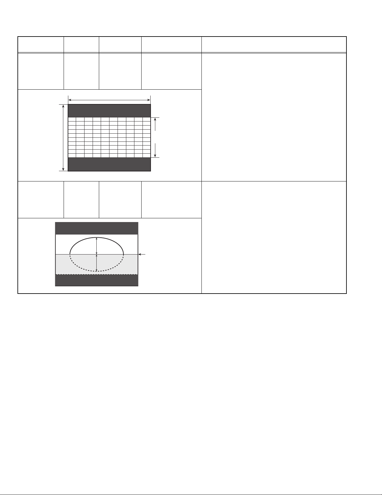
- PAL H. WIDTH -
(1) Receive a PAL crosshatch signal.
(2) Select 5. H-SIZE.
(3) Set the initial setting value of 5. H-SIZE.
(4) Adjust 5. H-SIZE to make the horizontal screen size
to 91% of the picture size.
- NTSC H. WIDTH -
(1) Receive a NTSC crosshatch signal.
(2) Make similar adjustment of NTSC H. WIDTH in the
same way as for "PAL H. WIDTH".
Picture size 100%
(No.YA256)1-25
Page 26
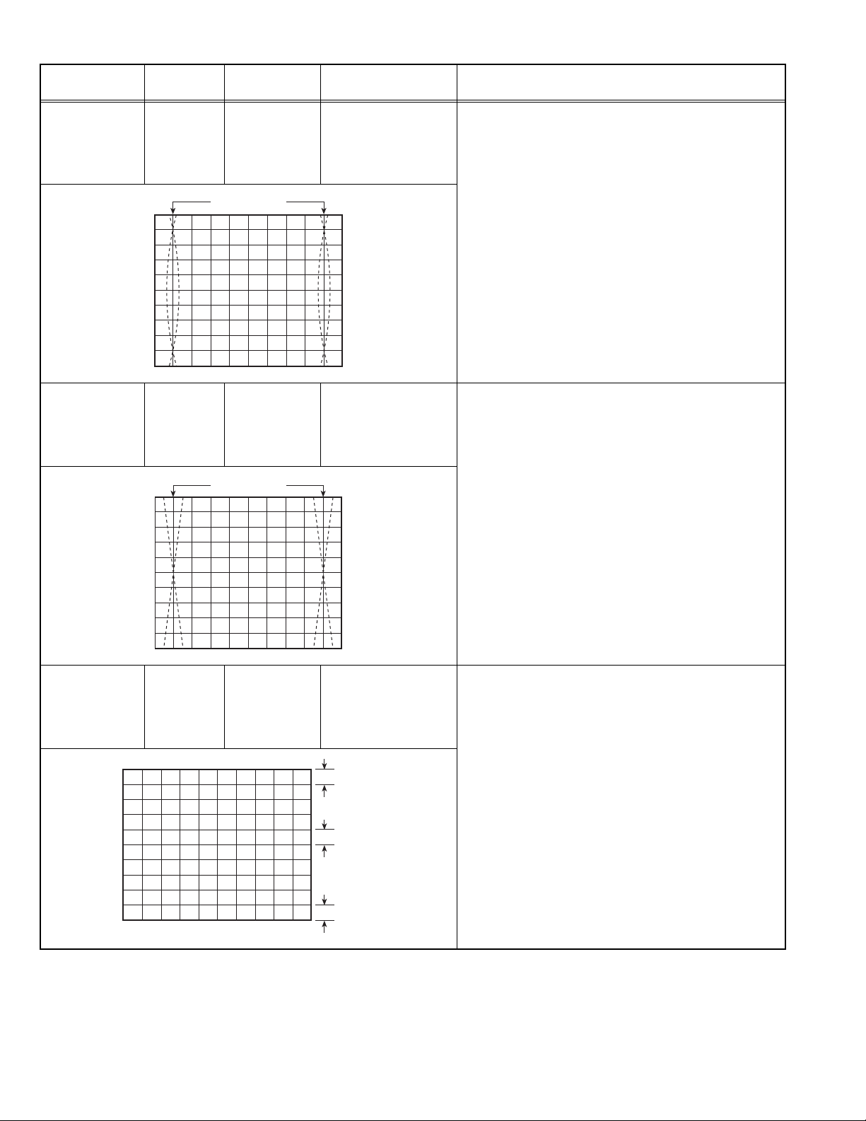
Item
SIDE PIN
adjustment
Measuring
instrument
Signal
generator
Remote
control unit
Test point Adjustment part Description
[4. DEF]
7. EW-PIN
- PAL SIDE PIN -
(1) Receive a PAL crosshatch signal.
(2) Select 7. EW-PIN.
(3) Set the initial setting value of 7. EW-PIN.
(4) Adjust 7. EW-PIN so that the first vertical lines at the
left and right edges on the screen are straight.
Straight
- NTSC SIDE PIN -
(1) Receive a NTSC crosshatch signal.
(2) Make similar adjustment of NTSC SIDE PIN in the
same way as for "PAL SIDE PIN".
TRAPEZIUM
adjustment
V.LINEARITY
adjustment
Signal
generator
Remote
control unit
Signal
generator
Remote
control unit
Parallel
[4.DEF]
6. TRAPEZ
[4. DEF]
12. V-S. CR
13. V-LIN
TOP
CENTER
- PAL TRAPEZIUM -
(1) Receive a PAL crosshatch signal.
(2) Select 6. TRAPEZ.
(3) Set the initial setting value of 6. TRAPEZ.
(4) Adjust 6. TRAPEZ so that the vertical lines at the left
and right edges on the screen are in parallel.
- NTSC TRAPEZIUM -
(1) Receive a NTSC crosshatch signal.
(2) Make similar adjustment of NTSC TRAPEZIUM in
the same way as for "PAL TRAPEZIUM".
- PAL V. LINEARITY -
(1) Receive a PAL crosshatch signal.
(2) Select 12. V-S.CR.
(3) Set the initial setting value of 12. V-S. CR.
(4) Select 13. V-LIN.
(5) Set the initial setting value of 13. V-LIN.
(6) Adjust 12. V-S. CR and 13. V-LIN so that the spaces
of each line on TOP, CENTER and BOTTOM
become uniform.
- NTSC V. LINEARITY -
(1) Receive a NTSC crosshatch signal.
(2) Make similar adjustment of NTSC V-S. CR in the
same way as for "PAL V-S. CR".
1-26 (No.YA256)
BOTTOM
Page 27
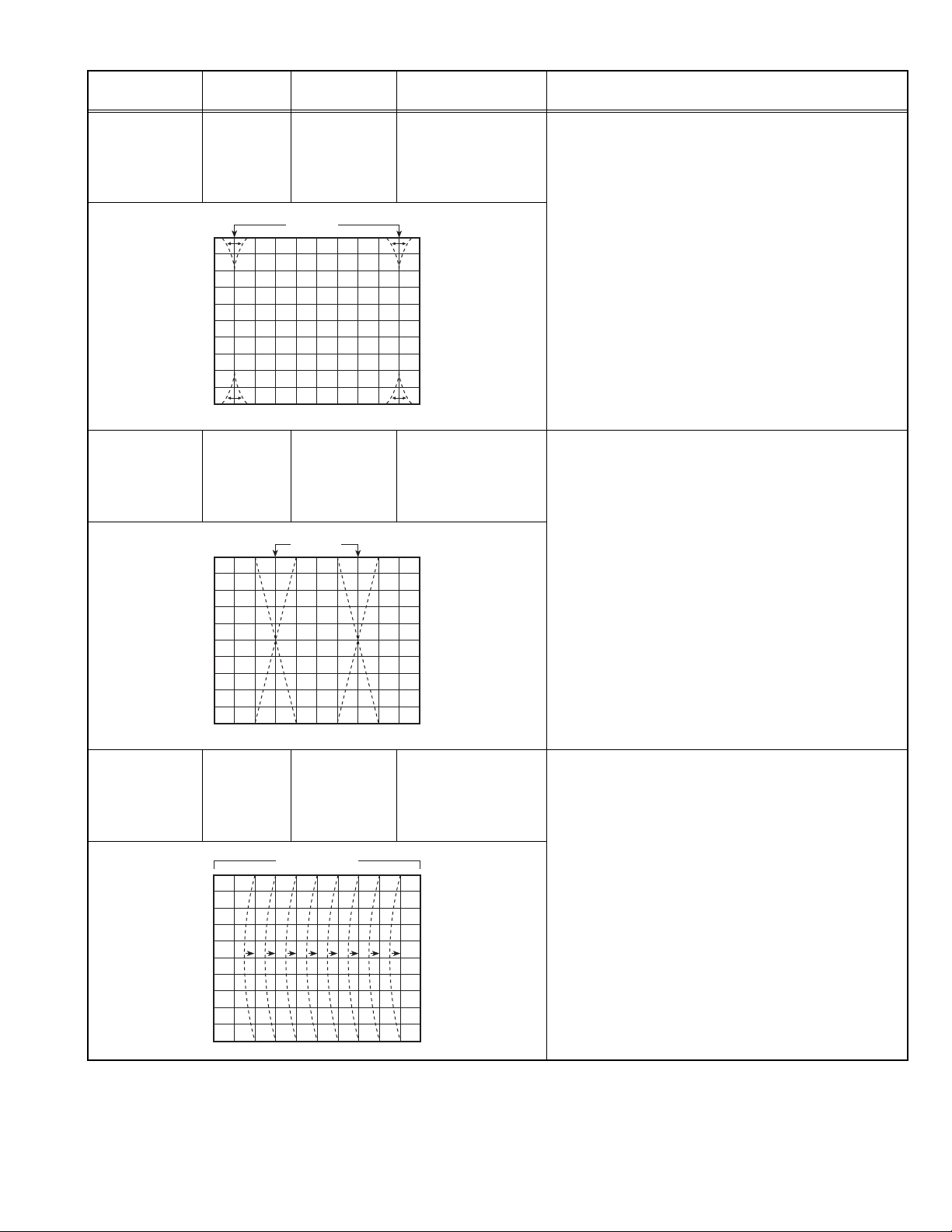
Item
CORNER PIN
adjustment
Measuring
instrument
Signal
generator
Remote
control unit
Test point Adjustment part Description
[4. DEF]
8. COR-UP
9. COR-LO
- PAL CORNER PIN -
(1) Receive a PAL crosshatch signal.
(2) Select 8. COR-UP.
(3) Set the initial setting value of 8. COR-UP.
(4) Select 9. COR-LO.
(5) Set the initial setting value of 9. COR-LO.
Straigt
(6) Adjust 8. COR-UP and 9. COR-LO so that the
vertical lines at the four corners on the screen are
straight.
- NTSC CORNER PIN -
(1) Receive a NTSC crosshatch signal.
(2) Make similar adjustment of NTSC CORNER in the
same way as for "PAL CORNER".
H. PARALLEL
adjustment
H. BOW
adjustment
Signal
generator
Remote
control unit
Signal
generator
Remote
control unit
Parallel
Straight
[4.DEF]
10. ANGLE
[4.DEF]
11. BOW
- PAL H. PARALLEL -
(1) Receive a PAL crosshatch signal.
(2) Select 10. ANGLE.
(3) Set the initial setting value of 10. ANGLE.
(4) Adjust 10. ANGLE to optimize the trapezium
distortion at the center of the screen.
- NTSC H. PARALLEL -
(1) Receive a NTSC crosshatch signal.
(2) Make similar adjustment of NTSC H. PARALLEL in
the same way as for "PAL H. PARALLEL".
- PAL H. BOW -
(1) Receive a PAL crosshatch signal.
(2) Select 11. BOW.
(3) Set the initial setting value of 11. BOW.
(4) Adjust 11. BOW to optimize the horizontal arc
distortion.
- NTSC H. BOW -
(1) Receive a NTSC crosshatch signal.
(2) Make similar adjustment of NTSC H. BOW in the
same way as for "PAL H. BOW".
(3) Press the [DISPLAY] key twice to return to the
normal screen.
(No.YA256)1-27
Page 28
COMPRESS : ON (16:9)
Item
V. HEIGHT
adjustment
Measuring
instrument
Signal
generator
Remote
control unit
Screen
size
V. SLOPE
adjustment
Signal
generator
Remote
control unit
Test point Adjustment part Description
[4.DEF]
14. V. ZOOM
3. V-SIZE
- PAL V. HEIGHT -
(1) Receive a PAL crosshatch signal of vertical
frequency 50Hz.
(2) Press the [MENU] key and select PICTURE.
(3) Select PICTURE FEATURES.
Screen size
(4) Select COMPRESS (16 : 9) and set COMPRESS to
ON.
(5) Select 4. DEF from the SERVICE MENU.
(6) Set the initial setting value of 14. V. ZOOM.
(7) Select 3. V-SIZE.
(8) Set the initial setting value of 3. V-SIZE.
Vertical
amplitude
(9) Adjust 3. V-SIZE to set the vertical amplitude of the
image to 305mm.
- NTSC V. HEIGHT -
(1) Receive a NTSC crosshatch signal of vertical
frequency 60Hz.
(2) Make similar adjustment of NTSC V. HEIGHT in
the same way as for "PAL V. HEIGHT".
[4.DEF]
2. V-SLOPE
- PAL V. SLOPE -
(1) Receive a PAL circle pattern signal of vertical
frequency 50Hz.
(2) Select 4. DEF from the SERVICE MENU.
(3) Select 2. V-SLOPE.
(4) Set the initial setting value of 2. V-SLOPE.
(5) Adjust 2. V-SLOPE to make "A = B".
(6) Press the [DISPLAY] key to return to SERVICE
A
Blanking
B
line
MENU screen.
- NTSC V. SLOPE -
(1) Receive a NTSC circle pattern signal of vertical
frequency 60Hz.
(2) Make similar adjustment of NTSC V-SLOPE in the
same way as for "PAL V-SLOPE".
1-28 (No.YA256)
Page 29

Item
SIDE PIN
adjustment
Measuring
instrument
Signal
generator
Remote
control unit
Test point Adjustment part Description
[4. DEF]
7. EW-PIN
- PAL SIDE PIN -
(1) Receive a PAL crosshatch signal.
(2) Select 7. EW-PIN.
(3) Set the initial setting value of 7. EW-PIN.
(4) Adjust 7. EW-PIN so that the first vertical lines at the
left and right edges on the screen are straight.
Straight
- NTSC SIDE PIN -
(1) Receive a NTSC crosshatch signal.
(2) Make similar adjustment of NTSC SIDE PIN in the
same way as for "PAL SIDE PIN".
TRAPEZIUM
adjustment
CORNER PIN
adjustment
Signal
generator
Remote
control unit
Signal
generator
Remote
control unit
Parallel
Straigt
[4. DEF]
6. TRAPEZ
[4. DEF]
8. COR-UP
9. COR-LO
- PAL TRAPEZIUM PIN -
(1) Receive a PAL crosshatch signal.
(2) Select 6. TRAPEZ.
(3) Set the initial setting value of 6. TRAPEZ.
(4) Adjust 6. TRAPEZ so that the vertical lines at the left
and right edges on the screen are in parallel.
- NTSC TRAPEZIUM PIN -
(1) Receive a NTSC crosshatch signal.
(2) Make similar adjustment of NTSC TRAPEZIUM in
the same way as for "PAL TRAPEZIUM".
- PAL CORNER PIN -
(1) Receive a PAL crosshatch signal.
(2) Select 8. COR-UP.
(3) Set the initial setting value of 8. COR-UP.
(4) Select 9. COR-LO.
(5) Set the initial setting value of 9. COR-LO.
(6) Adjust 8. COR-UP and 9. COR-LO so that the
vertical lines at the four corners on the screen are
straight.
- NTSC CORNER PIN -
(1) Receive a NTSC crosshatch signal.
(2) Make similar adjustment of NTSC CORNER in the
same way as for "PAL CORNER".
(3) Press the [DISPLAY] key twice to return to the
normal screen.
(No.YA256)1-29
Page 30

VIDEO - 2 SET: COMPONENT
Item
H. POSITION
adjustment
Measuring
instrument
Signal
generator
Remote
control unit
CD
4.7.7 VSM PRESET SETTING
Test point Adjustment part Description
[4. DEF]
4. H-CENT
(1) Receive a PAL circle pattern signal to VIDEO-2
component terminal.
(2) Select VIDEO-2 SET from the MENU and set
VIDEO-2 SET to COMPONENT.
(3) Select 4. DEF from the SERVICE MENU.
(4) Select 4. H-CENT.
(5) Set the initial setting value of 4. H-CENT.
(6) Adjust 4. H-CENT to make "C=D".
(7) Press the [DISPLAY] key twice to return to the
normal screen.
Item
VSM
PRESET
setting
Measuring
instrument
Remote
control unit
SUB MENU 5. VSM W/B
VSM PRESET BRIGHT
1. BRIGHT
Test point Adjustment part Description
[5. VSM W/B]
1. BRIGHT
2. CONT
3.COLOR
4. SHARP
5. HUE
1. R-DRIVE
2. G-DRIVE
3. B-DRIVE
(1) Select 5. VSM W/B from the SERVICE MENU.
(2) Select BRIGHT with the MENU [OK] key.
(3) Set the value of 1. BRIGHT ~ 5. HUE to the values
shown in the table.
(4) Respectively select the VSM PRESET mode for
SOFT and STANDARD.
(5) Select COOL with the MENU [OK] key.
(6) Set the values of 1. R-DRIVE ~ 3. B-DRIVE to the
value shown in the table.
(7) Select the W/B preset for WARM and NORMAL,
respectively.
(8) Press the [DISPLAY] key twice to return to the
normal screen.
***
[Setting Values for SUB 5. VSM W/B]
VSM preset
BRIGHT STANDARD SOFT
Setting item
1. BRIGHT 0+2
2. CONT +15 -3
3. COLOUR 00
4. SHARP 00
5. HUE 00
W/B preset
COOL WARMNORMAL
Setting item
1. R-DRIVE 0
2. G-DRIVE 0
3. B-DRIVE 0
0
0
0
0
+2
0
-10
-10
+10
-4
-12
1-30 (No.YA256)
Page 31

4.7.8 CONVERGENCE
STATIC CONVERGENCE ADJUSTMENT
(1) Input a crosshatch signal.
(2) Using 4-pole convergence magnets, overlap the red and
blue lines in the center of the screen (Fig.1) and turn them
to magenta (red/blue).
(3) Using 6-pole convergence magnets, overlap the magenta
(red/blue) and green lines in the center of the screen and
turn them to white.
(4) Repeat 2 and 3 above, and make best convergence.
(FRONT VIEW)
Fig.1
(FRONT VIEW)
DYNAMIC CONVERGENCE ADJUSTMENT
(1) Move the deflection yoke up and down and overlap the lines
in the periphery. (Fig. 2)
(2) Move the deflection yoke left to right and overlap the lines in
the periphery. (Fig. 3)
(3) Repeat 1 and 2 above, and make best convergence.
(4) Adjust XV by XV coil. (Fig.4)
• After adjustment, fix the wedge at the original position. Fasten
the retainer screw of the deflection yoke. Fix the P/C magnets
with glue.
RED
RED
BLUE
BLUE
GREEN
GREEN
Fig.2
(FRONT VIEW)
GREEN GREEN
RED
BLUE
Fig.3
BLUE
BLUE
RED
GREENGREEN
BLUE
RED
RED
RED
GREEN
BLUE
BLUE
GREEN
RED
(FRONT VIEW)
Xv
GREEN
Fig.4
(No.YA256)1-31
Page 32

SECTION 5
TROUBLESHOOTING
5.1 SELF CHECK FUNCTIONS
5.1.1 OUTLINE
This model has self check functions given below. When an abnormality has been detected, the SUB POWER is turned off and POWER
LED flashes to inform of the failure. An abnormality is detected by the signal input state of the control line connected to the
microcomputer.
5.1.2 SELF CHECK ITEMS
Check item Details of detection Method of detection State of abnormality
B1 over-current protection An over-current on the low B1
line is detected.
CRT neck broken protection Operation of CRT neck
protection circuit.
5.1.3 SELF CHECK INDICATING FUNCTION
When an abnormality has been detected at about 5 seconds
after the power was turned on, the SUB POWER is turned off
immediately and the POWER LED flashes.
The main microcomputer
detects the possible abnormality
at 24-msec. intervals and judges
the results in every 16 time. Of
the 16 times, if NG is detected
more than 9 times, it is judged
that there is an abnormality.
After about
5 seconds
When an abnormality has been
detected, the SUB-POWER is
turned off. While the SUBPOWER is being turned off, the
POWER key on the remote
control unit is not operational
until the power cord is
disconnected and connected
again.
Detection of
an abnormality
Powe r o n
Port
[ INDICATION BY THE POWER LED]
Item LED flashing intervals
B1 over-current protection / CRT neck broken protection 0.3 seconds
Start of
detection
Flashing LED
SUB-POWER OFF
1-32 (No.YA256)
Page 33

Victor Company of Japan, Limited
AV & MULTIMEDIA COMPANY VIDEO DISPLAY CATEGORY 12, 3-chome, Moriya-cho, kanagawa-ku, Yokohama, kanagawa-prefecture, 221-8528, Japan
(No.YA256)
Printed in Japan
VPT
Page 34

SERVICE MANUAL
FLAT COLOR TELEVISION
YA256B20055
BASIC CHASSIS
AV-29VT15/Z
Supplementary
AV-29VT15/Z is the models whose production place was changed based on AV-29VT15/R.
Therefore, this service manual describes only the items which differ from those of the AV-29VT15/R service
manual.
For details other than those described in this manual, please refer to the AV-29VT15/R service manual
(No.YA256, 2005/4).
HOW TO IDENTIFY MODELS
CW
"AV-29VT15ZAT" is added at the bottom of the Rating label.
AV-29VT15
Indicated
AV-29VT15ZAT
COPYRIGHT © 2005 Victor Company of Japan, Limited
No.YA256B
2005/5
Page 35

DIFFERENCE LIST
USING P.W. BOARD (Page 3-3)
P.W.B ASS'Y Name AV-29VT15/R AV-29VT15/Z DESCRIPTION
MAIN P.W.B SCW-1132A-Y2 SCW-1134A-H2 Non compatible
CRT SOCKET P.W.B SCW-3020A-Y2 SCW-3001A-H2 Non compatible
FRONT CONTROL P.W.B SCW-8010A-Y2 SCW-8001A-H2 Non compatible
EXPLODED VIEW PARTS LIST-1 (Page 3-3)
Ref. No.
100 GG10239-016A-HK GG10239-019A-H FRONT CABINET ASS'Y Inc. 101/102
101 GG20027-030A-H GG20027-033A-H DOOR
AV-29VT15/R AV-29VT15/Z
Part No.
PART NAME DESCRIPTION
EXPLODED VIEW PARTS LIST-2 (Page 3-4)
Ref. No.
V01 A68QCU770X52TD A68QCU770X52S PICTURE TUBE (ITC) Inc.DEF YOKE/PC MAGNET
12 GG10192-010A-HK GG10192-010A-H REAR COVER
16 QMPR830-165-JC QMPR340-165-K2 POWER CORD 1.65m BLACK
26 LC40226-005A-H LC40226-004A-H SPACER
27 GG20057-001A-H GG20057-002A-H SP HOLDER
29 GG20084-001A-D GG20024-001B-H RATING LABEL
40 SCW-1132A-Y2 SCW-1134A-H2 MAIN PWB
41 SCW-3020A-Y2 SCW-3001A-H2 CRT SOCKET PWB
42 SCW-8010A-Y2 SCW-8001A-H2 FRONT CONTROL PWB
AV-29VT15/R AV-29VT15/Z
Part No.
PART NAME DESCRIPTION
PRINTED WIRING BOARD PARTS LIST
MAIN P.W. BOARD ASS'Y (Page 3-7)
Part No.
Ref. No.
SCW-1132A-Y2 SCW-1134A-H2
D423 GP10DE-5009-T2 1N4003SG-T2 SI DIODE
C705 NDC31HJ-3R0X --- C CAPACITOR Delete
C706 NDC31HJ-3R0X --- C CAPACITOR Delete
CRT SOCKET P.W. BOARD ASS'Y (Page 3-10)
Part No.
Ref. No.
SCW-3020A-Y2 SCW-3001A-H2
D203 FR105SGT-T2 FR105GT-T3 SI DIODE
D204 FR105SGT-T2 FR105GT-T3 SI DIODE
CN0VM --- WJM0048-002A-E E-SI C WIRE C-F Addition
1-2 (No.YA256B)
PART NAME DESCRIPTIONAV-29VT15/R AV-29VT15/Z
PART NAME DESCRIPTIONAV-29VT15/R AV-29VT15/Z
Page 36

FRONT CONTROL P.W. BOARD ASS'Y (Page 3-11)
Part No.
Ref. No.
SCW-8010A-Y2 SCW-8001A-H2
R303 NRSA63J-124X NRSA63J-334X MG RESISTOR 330kΩ 1/16W J
PART NAME DESCRIPTIONAV-29VT15/R AV-29VT15/Z
PACKING PARTS LIST (Page 3-16)
Ref. No.
1 GG10359-001A-D GG10044-080A-H PACKING CASE
2 GG10193-007A-D GG10193-001E-H CUSHION ASS'Y 8pcs in 1set
6 GG30124-004A-D GG30097-004A-H POLY BAG
7 GG30123-001A-D GG30096-001A-H POLY BAG INST.
9 GGT0080-001A-D GGT0082-001A-H INST BOOK
14 GG40050-001A-D ---- POS LABEL Delete
AV-29VT15/R AV-29VT15/Z
Part No.
PART NAME DESCRIPTION
(No.YA256B)1-3
Page 37

SECTION 1
PRECAUTION
Please refer to "AV-29VT15/R (No.YA256)" about this section.
SECTION 2
SPECIFIC SERVICE INSTRUCTIONS
Please refer to "AV-29VT15/R (No.YA256)" about this section.
SECTION 3
DISASSEMBLY
Please refer to "AV-29VT15/R (No.YA256)" about this section.
SECTION 4
ADJUSTMENT
Please refer to "AV-29VT15/R (No.YA256)" about this section.
SECTION 5
TROUBLESHOOTING
Please refer to "AV-29VT15/R (No.YA256)" about this section.
1-4 (No.YA256B)
Page 38

Victor Company of Japan, Limited
AV & MULTIMEDIA COMPANY DISPLAY CATEGORY 12, 3-chome, Moriya-cho, Kanagawa-ku, Yokohama-city, Kanagawa-prefecture, 221-8528, Japan
(No.YA256B)
Printed in Japan
VPT
Page 39

COLOR TELEVISION EQUALIZER • CINEMA SURROUND • COMPONENT INPUT
Contents
AV-29VT15 AV-21VT15
AV-29VT35
AV-25VT15
Knowing your TV’s features ....................................................... 3
Remote control buttons and basic functions .............................. 4
TV buttons and functions ........................................................... 6
Setting up your TV ..................................................................... 7
Basic setting for picture.............................................................. 9
Advanced setting for picture ..................................................... 11
Basic setting for sound............................................................. 12
Advanced setting for sound ..................................................... 13
Favorite channel and video setting .......................................... 14
Customized setting .................................................................. 15
TV channel presetting .............................................................. 17
Additional preparation .............................................................. 18
Troubleshooting ....................................................................... 20
Specifications ........................................................................... 21
INSTRUCTIONS
GGT0080-001A-D
Page 40

Thank you for buying this JVC color television.
To make sure you understand how to use your new TV, please read this manual thoroughly before you begin.
WARNING: TO PREVENT FIRE OR SHOCK HAZARD, DO NOT
CAUTION: TO ENSURE PERSONAL SAFETY, OBSERVE THE
1 Operate only from the power source indicated on the rear of the TV.
2 Avoid damaging the power cord and mains plug. When unplugging the
TV, grasp the mains plug. Do not pull on the power cord.
3 Never block or cover the ventilation openings.
Never install the TV where good ventilation is unattainable.
When installing this TV, leave spaces for ventilation around the TV of
more than the minimum distances as shown.
4 Do not allow objects or liquid into the cabinet openings.
5 In the event of a fault, unplug the unit and call a service technician. Do
not attempt to repair it yourself or remove the rear cover.
6 The surface of the TV screen is easily damaged. Be very careful with it
when handling the TV. Should the TV screen become soiled, wipe it
with a soft dry cloth. Never rub it forcefully. Never use any cleaner or
detergent on it.
EXPOSE THIS APPLIANCE TO RAIN OR MOISTURE.
FOLLOWING RULES REGARDING THE USE OF THIS TV.
15 cm
10 cm 10 cm
15 cm
7 If you are not going to use this TV for a long period of time, be sure to
disconnect the AC plug from the AC socket.
8 The apparatus shall not be exposed to dripping or splashing and that
no objects filled with liquids, such as vases, shall be placed on the
apparatus.
2
Page 41

Knowing your TV’s features
Main features
MTS You can listen to the stereo sound or SAP from TV program broadcasting by MTS system.
CLOSED CAPTION You can display dialog on the screen from TV broadcasting with Closed Caption system.
FAVORITE CH (Channel) You can register up to four favorite channels for quick recall with one press.
AI ECO TV detects the brightness of your room and automatically adjust the picture brightness to a
AI VOLUME TV adjusts the volume automatically to the same level for all TV channels to avoid sudden
VNR You can reduce the picture noise when viewing noisy TV programs or video sources.
(SAP: Second audio program.)
You may also be able to display some information in text form if available.
suitable level for a better eye care.
change of the volume when selecting different TV channel.
1
Confirm your TV’s functions
Some functions written in this instruction manual may not be available for your TV.
2
Please see the chart below and check the functions that are equipped for your TV’s model number. The
model number is indicated at the rear of your TV. When you press a button concerned to a function that is
not available for your TV, it does not work and the logo “Ø” appears on the screen. For a function that is
not available for your TV, it is not displayed in the menu.
Model No.
No.
Function
1 *ECO __ _
2 *BASS _ ––
– PICTURE TILT __ –
– COMPRESS (16:9) __ _
AV-29VT35
AV-29VT15
AV-25VT15
AV-21VT15
3
Page 42

Remote control buttons and basic functions
No. Press To
1 POWER Turn on or off the TV from standby mode.
2 MENU/OK Display menu and confirm selected function.
3 5 / ∞ / 2 / 3 Select and adjust menu function.
4 CHANNEL -/+ Select the desired channel number.
5 VOLUME -/+ Adjust the volume level.
6 TV/VIDEO Select TV or video terminal input.
7 MUTING Turn off the volume.
8
DISPLAY/BACK
9
CLOSED CAPTION
! 0~9, 100+ Select the program number. For three digits program number, press 100+, then press the
" RETURN
Press this button again to resume the volume.
Display the program number or video terminal number on the screen.
On the other hand, you can use this button to return to the previous menu.
Display information in text which are broadcasted by some TV channels.
number button.
+
a) Return to the frequently view channel with one touch.
1 Choose the channel you want to register.
2 Press and hold RETURN+ button until “RETURN PLUS PROGRAMMED!” appears.
To cancel, press and hold RETURN+ button until “RETURN PLUS CANCELED!” appears.
b) Return to the previously viewed channel, if you have not set or have canceled the Return
channel as above.
4
Page 43

Remote control buttons and basic functions (continued)
How to operate menus and menus locations
To
Display the MENU
Display the top
menu
Display the 2nd
menu
Display the 3rd
menu
Return to the
previous menu
Choose the setting
of a function
Adjust the effect
level of a function
Display the sub
menu of a function.
Press the MENU/OK button 2.
Press 5/∞ buttons 3 to choose a
menu title. Then press MENU/OK
button 2.
Press 5/∞ buttons 3 to choose a
menu title. Then press MENU/OK
button 2.
Press 5/∞ buttons 3 to choose a
menu title. Then press MENU/OK
button 2.
Press the DISPLAY/BACK button*
8.
Press 5/∞ buttons 3 to choose
a function. Then press the 2/3
buttons 3 to change the setting.
Press 5/∞ buttons 3 to choose
a function. Then press the 2/3
buttons 3 to adjust the effect
level.
Press the 5/∞ buttons 3 to
choose a function. Then press
MENU/OK buttons 2 to display
the sub menu.
The following chart shows locations of functions in menus. In this manual,
location of a function is described as follows:
MENU Top menu
MENU 2nd menu
Top menu
Note: Some functions have the 4th menus as the sub-menus.
* To exit the menu, the on screen display will show BACK indicated in
blue. But it doesn’t refer to the blue button on the remote control.
Instead, it refers to the DISPLAY/BACK button on the remote control.
Operation
2nd menu
Note
To exit the MENU,
press the DISPLAY/
BACK button* 8 or
choose EXIT menu.
Press ∞ button 3 to
display the next page
for more functions.
–
Press the MENU/OK
button 2 to exit from
the menu.
–
3rd menu
Top menu 2nd menu Location 3rd menu Location
MENU INPUT EXT. INPUT P.16 – –
DISPLAY P.16 – –
CLOSED CAPTION P.15 – –
PICTURE PICTURE MODE P.9 – –
*If you want to
adjust PICTURE
SETTING menu,
you must set
PICTURE MODE
menu to USER.
SOUND AI VOLUME P.13 – –
*If you want to
adjust
EQUALIZER
menu, you must
set SOUND
MODE menu to
USER.
FEATURES OFF TIMER P.15 – –
INSTALL AUTO PROGRAM P.17 – –
EXIT – – – –
PICTURE SETTING P.10 – –
WHITE BALANCE P.10 – –
PICTURE – VNR P.15
FEATURES
MTS P.13 – –
SOUND MODE P.12 – –
EQUALIZER P.13 – –
BALANCE P.12 – –
SOUND TURBO P.12 – –
CINEMA SURROUND
SUPER BASS
CHILD LOCK P.15 – –
AI ECO SENSOR P.11 – –
CHANNEL SUMMARY
LANGUAGE
BLUE BACK P.11 – –
AUTO SHUTOFF P.16 – –
VIDEO-2 SETTING P.16 – –
AI ECO DISPLAY P.11 – –
FAVORITE CH SETTING
VIDEO SETTING P.14
COLOR SYSTEM P.9
COMPRESS (16:9) P.11
PICTURE TILT P.11
P.13 – –
P.12 – –
P.17 – –
P.16 – –
P.14
5
Page 44

TV buttons and functions
The illustrations shown below is for AV-29VT35 only,
which are used for explanation purpose.
Your TV may not look exactly the same as illustrated.
Front of the TV
AV-29VT35
!9 8765
VR
L/MONO
IN (VIDEO-3)
MENU
CHANNEL
VOLUME
TV/VIDEO
OK
EXIT
2
34
POWE
1
R
Rear of the TV
AV-29VT35
COMPONENT
VIDEO-1
(VIDEO-2)
OUTPUT
INPUT
V
Y
/
V
LRRL
C
B
/
MONO
C
R
#
$
"
BASS
SPEAKER
OUT
&
INPUT
S
OVER
V
L
/
MONO
R
%
No. Button/terminal Description Page
1 L (main power) Press to turn on or turn off the TV’s main power. –
2 POWER lamp Indicate the TV is being turned on or off. –
No color: TV’s main power is being turned off.
Red: TV’s main power is being turned on.
Note: When you turn off the power switch while TV is in standby
mode, the light of power lamp will be off in 10 -15 seconds.
3 ECO sensor –
4 Remote control sensor –
5 TV/ VIDEO Press to select TV or video mode. –
6 VOLUME -/+ Press to adjust the volume level. –
7 CHANNEL -/+ Press to select the desired channel. –
8 MENU Press to display the menu. –
9 IN (VIDEO-3) Video and audio input jacks for VIDEO-3 mode. 18
IN (VIDEO-2) Video and audio input jacks for VIDEO-2 mode. 18
! Headphone jack. 18
" Aerial socket. 7
# OUTPUT Video and audio output jacks. (The component video
signal cannot be output.) 18
$ COMPONENT Video or component video, and audio input jacks for
(VIDEO-2) INPUT VIDEO-2 mode. You can select the input signal by setting
the “VIDEO-2 SETTING” function (see page 16). 18
% VIDEO-1 INPUT
&
BASS SPEAKER OUT
Video or S-VIDEO, and audio input jacks for VIDEO-1 mode
Twin Port Bass Blaster Unit output terminal. 19
7
How to operate the menus with the TV button
TV button
Work as same as the button on the
remote control unit
Note
MENU MENU/OK button To display main menu and exit
menu after finish setting.
CHANNEL -/+ ∞/5 button To select menu function.
VOLUME -/+ 2/3 button To adjust the desired function.
6
Page 45

Setting up your TV
CAUTION
• Turn off the equipment including the TV before connecting.
1 Connecting the aerial cable.
VHF/UHF outdoor aerial
75-ohm coaxial cable (not supplied)
If you connect a VCR, connect the aerial output jack of your VCR
and the aerial jack on the TV with the aerial cable. Then connect the
output jacks of your VCR and the VIDEO-1 input jacks of the TV
with the video cable (or S-VIDEO cable if available) and audio
cables. For details, see the manual of your VCR.
Rear of TV
COMPONENT
VIDEO-1
(VIDEO-2)
OUTPUT
INPUT
INPUT
S
OVER
V
Y
V
/
V
LRRL
L
C
B
/
/
MONO
To video
output
To S-video
output
VCR
To audio
output
To aerial input
To RF
output
The illustration shown is just a sample. It may not be same as your
TV.
MONO
C
R
R
2 Connecting the compatible main plug to the AC outlet.
3 Inserting batteries into the remote control.
Insert two batteries by following the + and polarities and inserting the - end first.
CAUTION:
Follow the cautions printed on the batteries.
Notes:
• Use AA/R6/UM-3 dry cell batteries.
• It the remote control does not work properly, fit
new batteries. The supplied batteries are for
testing, not regular use.
4 Turn on the TV by pressing the main power button.
JVC logo appears on the screen.
VHF/UHF outdoor aerial
7
Page 46

Setting up your TV (continued)
5 Making the initial settings
Set up your TV by pressing MENU/OK button or waiting for 15 seconds, then the TV will operate by following steps as below:
LANGUAGE
ENGLISH
ESPAÑOL
Ê
S
PORTUGU
BACK
■
OK
AUTO PROGRAM
AIR
CABLE
BACK
■
OK
AUTO PROGRAM
22%
OK
CH 12
AUTO PROGRAM
SETUP TOUR RESTART?
OK
RESTART
■
NO
.
• Press 5/∞ button to
select your desired
language.
• Press 5/∞ button to
select AIR or CABLE,
press the MENU/OK
button.TV will start
searching for the
channels.
If the JVC logo does not appear, use AUTO PROGRAM function to make the initial settings. This function is located in the INSTALL
menu.
If the JVC logo appears, although you had made the initial settings, press the TV/VIDEO button to exit from initial settings.
• To stop AUTO
PROGRAM, press
MENU/OK button.
• Press the red button to
cancel the SETUP TOUR
RESTART function.
If you want to make initial
settings again when the
next time you turn on the
TV, press the MENU/OK
button to activate the
SETUP TOUR RESTART
function.
CHANNEL SUMMARY
CH/CC SKIP
CH02
■
CH03
■
CH04 ■
.
CH05
■
CH06
CH07
CH08
BACK ■
OK
• To complete the initial
setting, press the
MENU/OK button. To
set undesired
channels to be
skipped, see page 17.
■
SKIP
■
CANCEL
.
8
Page 47

Basic setting for picture
COLOR SYSTEM
You can select the appropriate color system when the picture is
not clear or no color appears.
Press the COLOR SYSTEM button to select a setting.
AUTO NTSC PAL-M PAL-N
.
To operate this function with a menu:
❇
MENU PICTURE menu
COLOR SYSTEM
For the color system in each country or region, see the table
below:
Area
South America
Argentina, Paraguay, Uruguay
Brazil
Chile, Peru, Bolivia, Colombia, Venezuela, Ecuador,
etc.
Country or Region
PICTURE FEATURES menu
System
PAL-N
PAL-M
NTSC
PICTURE MODE
You can choose the desired picture setting with one-touch.
Press the PICTURE MODE button to select a setting.
SOFT Softens contrast and sharpness.
BRIGHT Heightens contrast and sharpness.
STANDARD Standard picture setting.
USER You can change this picture setting as you like.
*TINT can only be adjusted in NTSC signal and 525i component
video signal.
To operate this function with a menu:
MENU PICTURE menu
To return the USER setting to the default, press the blue button
when the PICTURE SETTING menu appears.
❇ About the basic operations of the menu, please see the “How
to operate menus and menus locations” on page 5.
Select USER and adjust following items in the
PICTURE SETTING menu. (PICTURE, BRIGHT,
DETAIL, COLOR, TINT*)
PICTURE MODE
9
Page 48

Basic setting for picture (continued)
Adjusting the picture – USER
You can adjust the desired picture setting when selecting USER
in PICTURE MODE.
1 Select the USER in PICTURE MODE under PICTURE menu.
❇
MENU
USER
PICTURE menu
PICTURE MODE
2 Select the PICTURE SETTING in PICTURE menu, then adjust
the setting.
❇
MENU
PICTURE 2 : Lower 3 : Higher
BRIGHT 2 : Darker 3 : Brighter
DETAIL 2 : Softer 3 : Higher
COLOR 2 : Lighter 3 : Deeper
TINT* 2 : Reddish 3 : Greenish
*TINT can only be adjusted in NTSC signal and 525i component
video signal.
PICTURE menu
PICTURE SETTING
WHITE BALANCE
You can change the white balance of the picture to better match
the type of video being viewed.
Select the WHITE BALANCE in the PICTURE menu, then choose
the desired setting.
❇
MENU
NORMAL Normal white balance.
COOL Bluish white.
WARM Reddish white.
❇ About the basic operations of the menu, please see the “How
to operate menus and menus locations” on page 5.
PICTURE menu
WHITE BALANCE
10
Page 49
Advanced setting for picture
AI ECO SENSOR (ECO)
You can adjust TV screen contrast according to the brightness of
your room.
Press the ECO button to select the desired mode.
1 Mild contrast (recommended).
2 Even contrast.
OFF Cancel the function.
To operate this function with a menu:
❇
MENU
FEATURES menu
AI ECO SENSOR
You can display the graphic of AI ECO SENSOR on the screen.
Select the AI ECO DISPLAY in the INSTALL menu, then choose
ON or OFF.
❇
MENU INSTALL menu
AI ECO DISPLAY
Correcting the Slanting Picture (PICTURE TILT)
You can correct the picture tilt caused by the earth’s magnetic force.
1 Select the PICTURE TILT in the PICTURE FEATURES menu
under PICTURE menu, then press MENU/OK button.
❇
MENU
PICTURE TILT
The following display appears.
PICTURE menu
PICTURE TILT
PICTURE FEATURES menu
2 Press the 5/∞ buttons until the picture become level. Then
press the MENU/OK button.
COMPRESS (16:9)
You can convert a normal picture (4:3 aspect ratio) into a wide
picture (16:9 aspect ratio).
Select the COMPRESS (16:9) in the PICTURE FEATURES menu
under PICTURE menu, then choose ON or OFF.
❇
MENU
COMPRESS (16:9)
BLUE BACK
You can set the TV to automatically change to a blue screen and
mute the sound if the signal is weak or absent, or when there is
no input from an antenna.
Select the BLUE BACK in the INSTALL menu, then choose ON or
OFF.
❇
MENU
If you wish to continue viewing the poor picture, cancel the BLUE
BACK function.
❇ About the basic operations of the menu, please see the “How
to operate menus and menus locations” on page 5.
PICTURE menu
INSTALL menu
PICTURE FEATURES menu
BLUE BACK
BACK ■
OK
11
Page 50

Basic setting for sound
SUPER BASS (BASS)
You can enjoy powerful bass sound with the Twin Port Bass
Blaster unit.
Press the BASS button to select ON or OFF.
To operate this function with a menu:
❇
MENU
SOUND menu
SUPER BASS
For attaching the Twin Port Bass Blaster unit, please see in page
19.
SOUND MODE
You can choose the desired sound setting.
Select the SOUND MODE in SOUND menu, then choose the
setting.
❇
MENU
USER You can change this sound setting as you like.
DYNAMIC Emphasize on both vocal sound and music.
MUSIC Emphasize on music effect.
NEWS Emphasize on vocal sound.
SOUND menu
Select USER and adjust the frequencies in EQUALIZER
(100, 300, 1K, 3K, 8K Hz).
For details, see “EQUALIZER” on page 13.
SOUND MODE
BALANCE
You can adjust the volume balance between the left and right
speakers.
Select the BALANCE in SOUND menu, then adjust the setting.
❇
MENU
SOUND menu
BALANCE
SOUND TURBO
You can enjoy the emphatic low and high frequency levels.
Press the SOUND TURBO to select ON or OFF.
To operate this function with a menu:
❇
MENU SOUND menu
❇ About the basic operations of the menu, please see the “How
to operate menus and menus locations” on page 5.
SOUND TURBO
12
Page 51

Advanced setting for sound
CINEMA SURROUND
You can enjoy an enhanced sound for wider audience.
Press the CINEMA SURROUND button to select a setting.
OFF Cancel the function.
HIGH Listen to sound with more wider audience effect.
LOW Listen to sound with less wider audience effect.
MONO Listen to mono sound with stereo effect.
To operate this function with a menu:
❇
MENU
SOUND menu
CINEMA SURROUND
If slight volume distortion occurs when you select HIGH mode,
change the setting to LOW mode. The CINEMA SURROUND
effect will be less noticeable.
If you use CINEMA SURROUND and SOUND TURBO together,
volume distortion might occurs.
MTS
You can enjoy the stereo and SAP broadcasted programs.
Select the MTS in SOUND menu, then choose the desired mode.
❇
MENU
STEREO Select stereo sound.
SAP Select second audio programs.
MONO Select monaural sound.
This function is not available in video mode.
SOUND menu MTS
EQUALIZER
You can adjust the sound level of each frequencies when selecting
USER mode in SOUND MODE.
1 Select the USER in SOUND MODE under SOUND menu.
❇
MENU
SOUND menu
SOUND MODE USER
2 Select the EQUALIZER in SOUND menu.
❇
MENU SOUND menu
EQUALIZER
The following display appears.
EQUALIZER
IIIIIIIIIIII
IIIIIIIIIIIIIIIII
OK
IIIIIIIIIIIIIIIIIIIIIIIII
IIIIIIIIIIIIIIIIIIIIIII
IIIIIIIIIIII
100 300 1K 3K 8K Hz
BACK ■
3 Select and adjust the desired frequencies.
.
4 Press the MENU/OK button to exit the menu.
Adjust high frequency will affect higher pitch sound and vice versa.
AI VOLUME
You can adjust the volume of all the channels and video inputs to
the same level automatically.
Select the AI VOLUME in SOUND menu, then choose ON or OFF.
❇
MENU
SOUND menu
AI VOLUME
❇ About the basic operations of the menu, please see the “How
to operate menus and menus locations” on page 5.
13
Page 52
Favorite channel and video setting
To register the favorite channel
4 Select the desired item that you wish to adjust.
You can register and recall 4 favorite channels by using the color
buttons (red, green, yellow, blue).
1 In TV mode, select a TV channel (CH02-CH69, CC01-CC125)
you desired to register.
*TINT can only be adjusted in NTSC signal.
5 Press the MENU/OK button to exit the menu.
2 Press and hold a color button for 3 seconds or more.
“FAVORITE CHANNEL ■ PROGRAMMED!” appears on the
screen and current channel is registered.
3 To register other favorite channels, repeat Step 1 to 2.
To recall the favorite channel, press the color button.
When the TV is in menu mode, favorite channel function is not available.
To adjust favorite channel setting
(FAVORITE CH SETTING)
You can adjust the picture and sound settings for the favorite channels.
1 Display the PICTURE menu and select FAVORITE CH
SETTING in PICTURE FEATURES menu.
❇
MENU PICTURE menu
FAVORITE CH SETTING
PICTURE FEATURES menu
You can adjust the picture and sound settings for video inputs.
1 Display the PICTURE menu and select VIDEO SETTING in
2 Select VIDEO STATUS in VIDEO SETTING menu, then
3 Select EFFECT, then press 2/3 button
2 Select FAVORITE CHANNEL in FAVORITE CH SETTING
menu, then choose the desired favorite channel.
❇
FAVORITE CH SETTING
3 Select EFFECT, then press 2/3 button
to choose ON.
To cancel the settings, choose OFF.
14
FAVORITE CHANNEL
FAVORITE CH SETTING
FAVORITE CHANNEL
PICTURE
BRIGHT
DETAIL
COLOR
TINT
SOUND MODE USER
EFFECT ON
BACK ■
OK
.
■
CH02
4 Select the desired item that you wish to adjust.
*TINT can only be adjusted in NTSC signal and 525i component video signal.
5 Press the MENU/OK button to exit the menu.
❇ About the basic operations of the menu, please see the “How
PICTURE BRIGHT DETAIL COLOR
SOUND MODE (USER, DYNAMIC, MUSIC, NEWS)
TINT*
To adjust the video setting (VIDEO SETTING)
PICTURE FEATURES menu.
❇
MENU PICTURE menu
VIDEO SETTING
choose the desired video input.
❇
VIDEO SETTING VIDEO STATUS
to choose ON.
To cancel the settings, choose OFF.
PICTURE BRIGHT DETAIL COLOR
SOUND MODE (USER, DYNAMIC, MUSIC, NEWS)
to operate menus and menus locations” on page 5.
PICTURE FEATURES menu
VIDEO SETTING
VIDEO STATUS VIDEO-1
PICTURE
BRIGHT
DETAIL
COLOR
TINT
SOUND MODE USER
EFFECT ON
BACK ■
OK
■
RESET
TINT*
Page 53

Customized setting
VNR
You can reduce the picture noise.
Select the VNR in the PICTURE FEATURES menu under
PICTURE menu, then choose a setting of VNR function.
❇
MENU
VNR
OFF VNR is turned off.
AUTO Effect of VNR is automatically controlled.
MIN Effect of VNR becomes minimum level.
MAX Effect of VNR becomes maximum level.
PICTURE menu
PICTURE FEATURES menu
If you select MAX, the picture becomes softer even if the original
picture is sharp.
CLOSED CAPTION
If they are included in a program, you can view closed captions or
text information.
Press the CLOSED CAPTION button to select a setting.
OFF CLOSED CAPTION TEXT
1 Select the CLOSED CAPTION in INPUT menu, then choose
CAPTION or TEXT.
❇
MENU
INPUT menu
CLOSED CAPTION
2 Press the 2/3 button to select the desired caption or text
channel.
CHILD LOCK
You can disable the front control buttons of the TV.
Select the CHILD LOCK in the FEATURES menu, then choose
ON or OFF.
❇
MENU
FEATURES menu
CHILD LOCK
OFF TIMER
You can set the TV to turn off automatically to standby mode after
a set time.
Press the OFF TIMER button to select a desired period of time.
OFF TIMER
0 120
10
BACK ■
OK
To operate this function with a menu:
❇
MENU
FEATURES menu
When the elapsed of time left one minute, “GOOD NIGHT!”
appears on the screen.
You can display the OFF TIMER menu again to confirm or
change the remaining time.
❇ About the basic operations of the menu, please see the “How
to operate menus and menus locations” on page 5.
You can set the period of time
to a maximum of 120 minutes
in 10 minutes step.
OFF TIMER
15
Page 54

Customized setting (continued)
AUTO SHUTOFF
You can set the TV to turn off automatically when no signal is
received for about 15 minutes or longer after the end of a
broadcast.
Select AUTO SHUTOFF in INSTALL menu, then choose ON or
OFF.
❇
MENU INSTALL menu
AUTO SHUTOFF
The AUTO SHUTOFF function does not turn off the TV’s main
power.
The AUTO SHUTOFF function is not available in video mode.
VIDEO-2 SETTING
You can set the VIDEO-2 SETTING according to the video signal
output from the external devices connected to the VIDEO-2
terminal.
Select the VIDEO-2 SETTING in INSTALL menu, then choose a
setting.
❇
MENU INSTALL menu
VIDEO If a normal video signal (composite video signal) is
input.
COMPONENT If a component video signal (Y/CB/CR) is input.
For connecting methods, see “Additional Preparation” on page
18.
VIDEO-2 SETTING
EXT. INPUT (TV/VIDEO)
You can select TV or video terminal input with one touch.
Press the TV/VIDEO button to select an input.
To operate this function with a menu:
❇
MENU
INPUT menu
EXT. INPUT
DISPLAY
You can display the program number and video terminal number
on the screen.
Press the DISPLAY button to display the indication on the screen.
To operate this function with a menu:
❇
MENU
INPUT menu
DISPLAY
LANGUAGE
You can choose your desired on screen display language.
Select the LANGUAGE in the INSTALL menu, then choose a
language.
❇
MENU
❇ About the basic operations of the menu, please see the “How
to operate menus and menus locations” on page 5.
INSTALL menu
LANGUAGE
16
Page 55

TV channel presetting
To register the TV channels automatically
You can register the TV channels into the TV’s channel list
automatically.
1 Display the INSTALL menu.
❇
MENU
INSTALL menu
2 Choose AUTO PROGRAM, then press the MENU/OK button.
3 Press the 5/∞ button to select AIR or CABLE, then press the
MENU/OK button.
AUTO PROGRAM function starts, and the channels received
are registered automatically.
4 “SETUP TOUR RESTART?” appears.
To start the SETUP Press the MENU/OK button. Then proceed to
TOUR step 5 of “Setting up your TV” on page 8.
To skip the SETUP Press the Red button.
TOUR
5 The CHANNEL SUMMARY menu appears.
For details of “SETUP TOUR”, see page 8.
CHANNEL SUMMARY
You can set undesired channels to be skipped.
Channels are to be skipped cannot be selected by the
CHANNEL -/+ button.
1 Display the INSTALL menu.
❇
MENU
INSTALL menu
2 Choose CHANNEL SUMMARY, then press the MENU/OK
button.
CHANNEL SUMMARY menu appears.
CHANNEL SUMMARY
CH/CC SKIP
CH02
■
CH03
■
CH04
■
CH05
■
CH06
CH07
CH08
BACK ■
OK
.
■
■
SKIP
CANCEL
.
3 Choose the channel which you want to skip.
The skip can be set to all channels of AIR (CH02-CH69) and
CABLE (CC01-CC125).
4 Press the yellow button to skip the channel.
To cancel the skip, press the blue button.
5 Press the MENU/OK button to exit the menu.
❇ About the basic operations of the menu, please see the “How
to operate menus and menus locations” on page 5.
17
Page 56
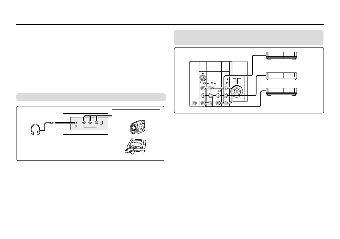
Additional preparation
The illustrations shown in this section are for AV-29VT35 and AV21YT15 only, which are used for explanation purpose. Your TV
may not look exactly the same as illustrated.
Before connecting
• Read the manuals provided with the devices for the proper
connection.
• Turn off all the devices including the TV.
• Note that connecting cables are not supplied.
Connecting to front video input terminal
Front of TV
Headphones
AV-29VT35
Camcorder or TV game
R
L/MONO
V
MENU
OK
IN (VIDEO-3)
.
Connecting to rear component/video input
terminal and output terminal
Rear of TV
AV-29VT35
COMPONENT
VIDEO-1
(VIDEO-2)
OUTPUT
INPUT
V
Y
/
V
LRRL
C
B
/
MONO
C
R
BASS
SPEAKER
OUT
S
OVER
V
L
R
INPUT
/
MONO
When you use VIDEO-1 INPUT, you should choose to connect
S-VIDEO or video input. If S-VIDEO connector and video input
are connected at the same time, no picture displays on the
screen and the message “PLEASE DISCONNECT VIDEO-1
CABLE!” appears. In this case, you should disconnect either SVIDEO or video input.
When connecting to COMPONENT (VIDEO-2) input, depending
on the connection, choose the appropriate video input using the
menu (see page 16).
VCR (for playing)
DVD player (composite signals)
VCR (for recording)
DVD player
(component video signals)
.
.
18
Page 57

Additional preparation (continued)
Attaching the Twin Port Bass Blaster Unit
<AV-29VT35 only>
The Twin Port Bass Blaster Unit is packaged together with the
TV. Before you use the TV, mount the Twin Port Bass Blaster unit
correctly on the TV.
• The SUPER BASS (BASS) function do not work unless the
Twin Port Bass Blaster Unit is connected correctly to the TV.
For details on the SUPER BASS (BASS) function, see page
12.
1 Place the unit on top of the TV making sure that the mounting
pin on the bottom of the unit fits into the mounting hole on the
top of the TV.
• When you mount the unit, make sure that the mounting pin
fits properly into the mounting hole. Otherwise, it may slide
off the top of the TV. This may cause damage or cause
unexpected injury.
Twin Port
Bass Blaster
Unit
CAUTION:
The Twin Port Bass Blaster Unit is just placed on top of the TV
and is not held in place by a screw. When using the unit, pay
attention to the following cautions. Otherwise, the unit or TV may
fall over and be damaged, or cause unexpected injury.
• Do not rest your hands or elbows on the Twin Port Bass
Blaster Unit.
• Do not move the TV with the Twin Port Blaster Unit mounted
on top of the TV. Before you move the TV, be sure to remove
the unit.
• Do not move the TV by holding the Twin Port Bass Blaster
Unit.
2
Firmly insert the Twin Port Bass Blaster Unit connector into the
BASS SPEAKER OUT terminal.
COMPONENT
VIDEO-1
(
)
OUTPUT
VIDEO-2
INPUT
INPUT
S
OVER
Y
BASS
SPEAKER
OUT
V
L
R
/
MONO
C
C
V
/
V
B
/
R
19
Page 58

Troubleshooting
If a problem occurs when you are using the TV, check the below
troubleshooting guide before calling for repair.
• No picture,
no sound
• Snowy picture
• Stripes appear on
the picture
• Double-pictures
(ghosting) occur
• Poor picture
• White and bright still
image look as if it
were colored
• Top of the image
from software
products or video
tape is distorted
• Poor sound
• Stereo or bilingual
sound is unclear
• Deactivate the BLUE BACK function if it is turned
on.
• Check the aerial cable and its connection with the
TV.
• Interference occurs caused by other devices such
as an amplifier, personal computer, or a hair drier.
Move such devices away from your TV.
• Interference occurs caused by signal reflecting
from mountains or building. Try to adjust the
aerial’s direction or use a better directionality
antenna.
• Choose the appropriate color system. Refer to
“COLOR SYSTEM” on page 9.
• Adjust the COLOR or BRIGHT setting. Refer to
“Adjusting the picture - USER” on page 10.
• Inevitable phenomenon due to the nature of the
picture tube. This is not a malfunction.
• This is due to the condition of the video signal
whereby the image was not recorded properly.
This is not a malfunction.
• Adjust the sound frequency properly. Refer to
“EQUALIZER” on page 13.
• TV channel reception is poor. Change the stereo/
bilingual mode to mono sound (see page 13).
• Cannot operate the
remote control
• Cannot operate the
menus
• Cannot operate the
front control buttons
• TV is turned off
suddenly
• Color patches
appear at the corner
of the screen
• Picture is tilted
• Image takes a short
period to be
displayed
• TV may emitted
crackling sound
• Feel a slight electric
shock when
touching the TV
screen
• The batteries may be exhausted. Replace with
new batteries (see page 7).
• Ensure that you are operating the remote less
than seven meters from the front of your TV.
• Press TV/VIDEO button to return to TV mode and
try operating the menus.
• Deactivate the CHILD LOCK function if it is turned
on (see page 15).
• This may due to the AUTO SHUTOFF function is
activated. Press the POWER button to turn on the
TV.
• This may due to the magnetized device such as a
speaker near to your TV. Keep the device apart
from your TV. Alternately, you can also use the
magnetic-shielded speaker.
• This may due to the earth magnetism. Refer to
“PICTURE TILT” on page 11 to correct the tilt.
• Image required time to stabilize before display.
This is not a malfunction.
• This is due to a sudden change in temperature
and it is not a malfunction. If the crackling sound
is too frequent, request your service technician for
inspection.
• This is due to the static electricity of the picture
tube and it will not harm the human body. This is
not a malfunction.
20
Page 59

Specifications
TV RF systems
M, N
Color systems
NTSC, PAL-M, PAL-N
Receiving channels
VHF low channel (VL), VHF high channel (VH), UHF channel (U)
Receives cable channels in mid band, super band and hyper band.
External input / output
VIDEO-1: S-video input, VIDEO input, AUDIO L/R input
VIDEO-2/COMPONENT: VIDEO input, AUDIO L/R input, COMPONENT VIDEO (Y/CB/CR) input
VIDEO-3: VIDEO input, AUDIO L/R input
OUTPUT: VIDEO output, AUDIO L/R output
Headphone jack: Stereo mini jack (3.5 mm diameter)
Sound-multiplex systems
MTS (Multi-Channel Television Sound)
Design and specifications subject to change without notice.
21
Page 60

MEMO
22
Page 61

MEMO
23
Page 62

© 2004 Victor Company of Japan, Limited
1204-FLE-JMT
Page 63

PARTS LIST
CAUTION
J The parts identified by the symbol are important for the safety . Whenever replacing these parts, be sure to use specified ones to secure the
safety.
J The parts not indicated in this Parts List and those which are filled with lines --- in the Parts No. columns will not be supplied.
J P.W. BOARD Ass'y will not be supplied, but those which are filled with the Parts No. in the Parts No. columns will be supplied.
ABBREVIATIONS OF RESISTORS, CAPACITORS AND TOLERANCES
RESISTORS CAPACITORS
CR Carbon Resistor C CAP. Ceramic Capacitor
FR Fusible Resistor E CAP. Electrolytic Capacitor
PR Plate Resistor M CAP. Mylar Capacitor
VR Variable Resistor CH CAP. Chip Capacitor
HV R High Voltage Resistor HV CAP. High Voltage Capacitor
MF R Metal Film Resistor MF CAP. Metalized Film Capacitor
MG R Metal Glazed Resistor MM CAP. Metalized Mylar Capacitor
MP R Metal Plate Resistor MP CAP. Metalized Polystyrol Capacitor
OM R Metal Oxide Film Resistor PP CAP. Polypropylene Capacitor
CMF R Coating Metal Film Resistor PS CAP. Polystyrol Capacitor
UNF R Non-Flammable Resistor TF CAP. Thin Film Capacitor
CH V R Chip Variable Resistor MPP CAP. Metalized Polypropylene Capacitor
CH MG R Chip Metal Glazed Resistor TAN. CAP. Tantalum Capacitor
COMP. R Composition Resistor CH C CAP. Chip Ceramic Capacitor
LPTC R Linear Positive Temperature Coefficient Resistor BP E CAP. Bi-Polar Electrolytic Capacitor
CH AL E CAP. Chip Aluminum Electrolytic Capacitor
CH AL BP CAP. Chip Aluminum Bi-Polar Capacitor
CH TAN. E CAP. Chip Tantalum Electrolytic Capacitor
CH AL BP E CAP. Chip Tantalum Bi-Polar Electrolytic Capacitor
RESISTORS
FGJ KMNRHZ P
±1% ±2% ±5% ±10% ±20% ±30%
+30%
-10%
+50%
-10%
+80%
-20%
+100%
-0%
(No.YA256)3-1
Page 64

CONTENTS
USING P.W. BOARD & REMOTE CONTROL UNIT ................................................................................................... 3-3
EXPLODED VIEW PARTS LIST -1 ............................................................................................................................. 3-3
EXPLODED VIEW -1 ................................................................................................................................................... 3-3
EXPLODED VIEW PARTS LIST -2 ............................................................................................................................. 3-4
EXPLODED VIEW -2 ................................................................................................................................................... 3-5
EXPLODED VIEW PARTS LIST -3 [AV-29VT35/R] ................................................................................................... 3-6
EXPLODED VIEW -3 ................................................................................................................................................... 3-6
PRINTED WIRING BOARD PARTS LIST [AV-29VT15/R] ......................................................................................... 3-7
MAIN P.W. BOARD ASS'Y (SCW-1132A-Y2) ................................................................................................... 3-7
CRT SOCKET P.W. BOARD ASS'Y (SCW-3020A-Y2) ................................................................................... 3-10
FRONT CONTROL P.W. BOARD ASS'Y (SCW-8010A-Y2) ........................................................................... 3-11
PRINTED WIRING BOARD PARTS LIST [AV-29VT35/R] ....................................................................................... 3-12
MAIN P.W. BOARD ASS'Y (SCW-1133A-Y2) ................................................................................................. 3-12
CRT SOCKET P.W. BOARD ASS'Y (SCW-3020A-Y2) ................................................................................... 3-15
FRONT CONTROL P.W. BOARD ASS'Y (SCW-8010A-Y2) ........................................................................... 3-15
REMOTE CONTROL UNIT PARTS LIST (RM-C1288-1H) ....................................................................................... 3-16
PACKING ................................................................................................................................................................... 3-16
PACKING PARTS LIST ............................................................................................................................................. 3-16
3-2(No.YA256)
Page 65

USING P.W. BOARD & REMOTE CONTROL UNIT
P.W.B ASS'Y AV-29VT15/R AV-29VT35/R
MAIN P.W.B SCW-1132A-Y2 SCW-1133A-Y2
CRT SOCKET P.W.B SCW-3020A-Y2 ←
FRONT CONTROL P.W.B SCW-8010A-Y2 ←
REMOTE CONTROL UNIT RM-C1288-1H ←
EXPLODED VIEW PARTS LIST -1
Ref.No. Part No. Part Name Description Local
1 GG20028-003A-H OPERATION SHEET
2 CM48229-00A-C DOOR LATCH
3 LC41540-002C JVC MARK
4 QYNSS2000P PUSH NUT M2
5 CM35235-003-H SPRING
6 GG30050-001C-H REMOCON LENS
7 GG30049-001D-H LED LENS
100 GG10239-016A-HK FRONT CABINET ASS'Y Inc.101,102
101 GG20027-030A-H DOOR
102 GG30048-003A-H POWER KNOB
EXPLODED VIEW -1
100
3
4
6
7
1
101
2
5
102
(No.YA256)3-3
Page 66

EXPLODED VIEW PARTS LIST -2
Ref.No. Part No. Part Name Description Local
V01 A68QCU770X52TD PICTURE TUBE(ITC) Inc.DEF YOKE,PC MAGNET
L01 QQW0187-001 DEG COIL Inc.ROTATION COIL
T522 QQH0184-001 FB TRANSF
11 QYSBSFG4016ZA TAP SCREW M4 x 16mm(x11)
12 GG10192-010A-HK REAR COVER AV-29VT15/R
12 GG10192-011A-HK REAR COVER AV-29VT35/R
13 QYSBSF3012MA TAP SCREW M3 x 12mm(x4)
14 LC11064-008A-H AV TERMINAL BOARD AV-29VT15/R
14 LC11064-007A-H AV TERMINAL BOARD AV-29VT35/R
15 CM23167-A01-H POWER CORD CLAMP
16 QMPR830-165-JC POWER CORD 1.65m BLACK
17 LC11061-002A-H CHASSIS BASE
18 LC11062-003A-H CONTROL BASE
19 QUQ212-0916CH FFC WIRE 9pin 16cm
20 WJS0052-001A E-FL/RB WIRE
23 A48457-3-H SPRING
24 WJY0018-001A BRAIDED ASS'Y
25 CHGB0017-0C BRAIDED SUB ASS'Y (x2)
26 LC30103-001B-H CHASSIS ADAPTER (x2)
27 GG40046-001A-H TAP SCREW (x4)
28 LC40226-004A-H SPACER (x4)
29 GG20057-001A-H SP HOLDER (x4)
30 QAS0139-001 SPEAKER (x2) SP01,SP02
31 GG20084-001A-D RATING LABEL AV-29VT15/R
31 GG20084-002A-D RATING LABEL AV-29VT35/R
40 SCW-1132A-Y2 MAIN PWB AV-29VT15/R
40 SCW-1133A-Y2 MAIN PWB AV-29VT35/R
41 SCW-3020A-Y2 CRT SOCKET PWB
42 SCW-8010A-Y2 FRONT CONTROL PWB
3-4(No.YA256)
Page 67

EXPLODED VIEW -2
27
27
26
L01
28
FRONT CABINET
V01
22
26
24
25
23
42
18
24
21
27
27
26
41
19
26
25
28
42
20
40
T522
14
17
BASS SPEAKER OUT JACK
[AV-29VT35/R]
15
16
12
11
TWIN PORT
BASS BLASTER UNIT
[AV-29VT35/R]
29
13
(No.YA256)3-5
Page 68

EXPLODED VIEW PARTS LIST -3 [AV-29VT35/R]
Ref.No. Part No. Part Name Description Local
50 LC40352-001A-H RUBBER SHEET (x4)
51 QYSBSFG4016ZA TAP SCREW M4 x 16mm(x13)
52 GG10141-001C-H BASS BOTTOM
53 LC41211-001A SOUND ABSORBER
54 QYSBSFG4016ZA TAP SCREW M4 x 16mm(x4)
55 QAS0118-001 SPEAKER SP03
56 WJJ0266-002A E-SIC WIRE C-C
57 GG30022-001A-H BASS DUCT R (x2)
58 GG10140-001C-H BASS TOP
EXPLODED VIEW -3
50
51
50
53
54
51
55
51
51
52
57
54
3-6(No.YA256)
57
56
58
Page 69

PRINTED WIRING BOARD PARTS LIST [AV-29VT15/R]
MAIN P.W. BOARD ASS'Y (SCW-1132A-Y2)
Ref No. Part No. Part Name Description Local
IC401 LA78041 IC
IC601 AN5277 IC
IC701 TDA12027-NTSC IC(MCU) (SERVICE)
IC702 AT24C16-29VT35R IC (SERVICE)
IC921 STR-W6756-F5 SW IC
IC951 SE135N IC
IC972 BA33BC0T REGULATOR IC
IC973 PQ120RDA1SZ IC
IC974 MM1561JF-X IC
IC975 PQ050RDA1SZ IC
IC976 MM1561JF-X IC
Q101 2SC5397/CD/-T TRANSISTOR
Q341 2SA1530A/QR/-X TRANSISTOR
Q461 RDN050N20 POWER MOS FET
Q521 BSN304-T TRANSISTOR
Q522 TT2142-YD TRANSISTOR
Q571 2SA1208/ST/Z1-T TRANSISTOR
Q572 UN2212-X DIGI TRANSISTOR
Q601 2SA1530A/QR/-X TRANSISTOR
Q602 2SA1530A/QR/-X TRANSISTOR
Q603 UN2226-X DIGI TRANSISTOR
Q605 UN2226-X DIGI TRANSISTOR
Q607 2SC3928A/QR/-X TRANSISTOR
Q608 2SC3928A/QR/-X TRANSISTOR
Q609 UN2212-X DIGI TRANSISTOR
Q611 UN2212-X DIGI TRANSISTOR
Q702 2SC3928A/QR/-X TRANSISTOR
Q703 2SA1530A/QR/-X TRANSISTOR
Q704 2SC3928A/QR/-X TRANSISTOR
Q705 SSM3K02F-X MOS FET
Q706 SSM3K02F-X MOS FET
Q707 2SC3928A/QR/-X TRANSISTOR
Q708 2SA1530A/QR/-X TRANSISTOR
Q791 DTC124ESA-T DIGI TRANSISTOR
Q801 KTA1267/YG/-T TRANSISTOR
Q803 UN2226-X DIGI TRANSISTOR
Q804 UN2226-X DIGI TRANSISTOR
Q805 2SA1530A/QR/-X TRANSISTOR
Q921 2SC3852A POW TRANSISTOR
Q951 2SC3928A/QR/-X TRANSISTOR
Q952 2SC3928A/QR/-X TRANSISTOR
Q957 2SC3928A/QR/-X TRANSISTOR
Q958 2SA1013/RO/-T TRANSISTOR
D341 MA111-X SI DIODE
D342 MA111-X SI DIODE
D343 MA111-X SI DIODE
D345 MA111-X SI DIODE
D423 GP10DE-5009-T2 SI DIODE
D471 1SR124-400A-T2 SI DIODE
D472 MA111-X SI DIODE
D521 RH3G-F1 SI DIODE
D522 RU4AM-LFT2 SI DIODE
D523 FR105GT-T3 SI DIODE
D524 MA8091/H/-X Z DIODE
D530 FR105GT-T3 SI DIODE
D551 FR105GT-T3 SI DIODE
D552 FR105GT-T3 SI DIODE
D554 MA8051/L/-X Z DIODE
D571 MA8075/H/-X Z DIODE
D581 FR105GT-T3 SI DIODE
D601 MA111-X SI DIODE
D603 MA111-X SI DIODE
D604 MA8300/H/-X Z DIODE
D605 MA8300/H/-X Z DIODE
D607 MA111-X SI DIODE
D701 MA111-X SI DIODE
D702 MA8091/H/-X Z DIODE
D704 MA8091/H/-X Z DIODE
D705 MA8039/H/-X Z DIODE
D706 MA8036-X Z DIODE
D707 MA111-X SI DIODE
D708 MA111-X SI DIODE
D709 MA111-X SI DIODE
D710 MA8091/H/-X Z DIODE
D711 MA111-X SI DIODE
D712 MA111-X SI DIODE
D714 MA8030/H/-X Z DIODE
D751 MA8091/H/-X Z DIODE
D753 MA8091/H/-X Z DIODE
D791 MA8062/M/-X Z DIODE
Ref No. Part No. Part Name Description Local
D801 NCB21HK-152X C CAPACITOR 1500pF 50V K
D802 NCB21HK-152X C CAPACITOR 1500pF 50V K
D803 NCB21HK-152X C CAPACITOR 1500pF 50V K
D804 NCB21HK-152X C CAPACITOR 1500pF 50V K
D810 MA8091/H/-X Z DIODE
D811 MA8091/H/-X Z DIODE
D812 MA8091/H/-X Z DIODE
D813 MA8091/H/-X Z DIODE
D814 MA8091/H/-X Z DIODE
D815 MA8091/H/-X Z DIODE
D901 GSIB460-S1 BRIDGE DIODE
D921 RGP10J-5025-T3 SI DIODE
D922 1SS133-T2 SI DIODE
D923 MA111-X SI DIODE
D924 MA8330/M/-X Z DIODE
D925 RGP10J-5025-T3 SI DIODE
D926 RGP10M-5010-T3 SI DIODE
D927 MA111-X SI DIODE
D928 MA8240/M/-X Z DIODE
D929 MA111-X SI DIODE
D930 MA8240/M/-X Z DIODE
D931 MA8062/M/-X Z DIODE
D932 MTZJ36A-T2 Z DIODE
D933 MTZJ9.1C-T2 Z DIODE
D934 MTZJ9.1C-T2 Z DIODE
D935 MTZJ9.1C-T2 Z DIODE
D936 1SS133-T2 SI DIODE
D951 RU4AM-LFT2 SI DIODE
D952 FMX-G12S SI DIODE
D953 FR105GT-T3 SI DIODE
D954 FR105GT-T3 SI DIODE
D955 FMX-G12S SI DIODE
D957 MA8039/H/-X Z DIODE
D959 NRSA63J-0R0X MG RESISTOR 0Ω 1/16W J
D960 NRSA63J-0R0X MG RESISTOR 0Ω 1/16W J
D962 MA8330/M/-X Z DIODE
D970 MA8082/M/-X Z DIODE
D971 MA111-X SI DIODE
D972 1SR124-400A-T2 SI DIODE
D973 MA111-X SI DIODE
D975 MA111-X SI DIODE
D977 MA111-X SI DIODE
C001 NCB31HK-103X C CAPACITOR 0.01uF 50V K
C002 QETN1HM-106Z E CAPACITOR 10uF 50V M
C003 NCB31HK-104X C CAPACITOR 0.1uF 50V K
C004 QETN1CM-477Z E CAPACITOR 470uF 16V M
C005 NCB31HK-222X C CAPACITOR 2200pF 50V K
C006 QETN1CM-336Z E CAPACITOR 33uF 16V M
C101 NCB31HK-103X C CAPACITOR 0.01uF 50V K
C102 NCB31HK-103X C CAPACITOR 0.01uF 50V K
C103 NCB31HK-103X C CAPACITOR 0.01uF 50V K
C104 QETN1EM-476Z E CAPACITOR 47uF 25V M
C106 NCB31HK-103X C CAPACITOR 0.01uF 50V K
C109 NRSA63J-0R0X MG RESISTOR 0Ω 1/16W J
C110 NCB31HK-104X C CAPACITOR 0.1uF 50V K
C111 QETN1CM-477Z E CAPACITOR 470uF 16V M
C341 QETN1CM-227Z E CAPACITOR 220uF 16V M
C422 QCS32HJ-560Z C CAPACITOR 56pF 500V J
C423 NDC31HJ-102X C CAPACITOR 1000pF 50V J
C424 QFLC2AJ-683Z M CAPACITOR 0.068uF 100V J
C427 QETN1VM-108Z E CAPACITOR 1000uF 35V M
C428 QEHR1VM-107Z E CAPACITOR 100uF 35V M
C430 QFLC2AJ-563Z M CAPACITOR 0.056uF 100V J
C431 NCB31HK-104X C CAPACITOR 0.1uF 50V K
C435 NCF21HZ-334X C CAPACITOR 0.33uF 50V Z
C436 NCF21HZ-334X C CAPACITOR 0.33uF 50V Z
C471 QETN1HM-106Z E CAPACITOR 10uF 50V M
C520 NRSA63J-0R0X MG RESISTOR 0
C521 QCB31HK-332Z C CAPACITOR 3300pF 50V K
C522 QFLC1HJ-223Z M CAPACITOR 0.022uF 50V J
C523 QETN1VM-476Z E CAPACITOR 47uF 35V M
C524 QFZ0196-202 MPP CAPACITOR 2000pF 1.5kV H
C525 QFZ0196-123 MPP CAPACITOR 0.012uF 1.5kV H
C526 QFZ0196-252 MPP CAPACITOR 2500pF 1.5kV H
C527 QFZ0197-204 MPP CAPACITOR 0.2uF 250V J
C528 QFP32JJ-223 PP CAPACITOR 0.022uF 630V J
C529 QENC2AM-225Z BP E CAPACITOR 2.2uF 100V M
C530 QCB32HK-561Z C CAPACITOR 560pF 500V K
C531 QEZ0195-475Z BP E CAPACITOR 4.7uF 50V M
C532 QETN2EM-106Z E CAPACITOR 10uF 250V M
C551 QCB32HK-561Z C CAPACITOR 560pF 500V K
C552 QCB32HK-561Z C CAPACITOR 560pF 500V K
C553 QEHR1EM-108Z E CAPACITOR 1000uF 25V M
Ω
1/16W J
(No.YA256)3-7
Page 70

Ref No. Part No. Part Name Description Local
Ref No. Part No. Part Name Description Local
C554 QEHR1EM-108Z E CAPACITOR 1000uF 25V M
C555 QFLC2AJ-103Z M CAPACITOR 0.01uF 100V J
C571 QETM2CM-227 E CAPACITOR 220uF 160V M
C572 QETN1CM-107Z E CAPACITOR 100uF 16V M
C573 QETN1EM-476Z E CAPACITOR 47uF 25V M
C581 QFVF1HJ-104Z MF CAPACITOR 0.1uF 50V J
C582 QFZ0197-204 MPP CAPACITOR 0.2uF 250V J
C601 QETN1HM-106Z E CAPACITOR 10uF 50V M
C602 QETN1HM-106Z E CAPACITOR 10uF 50V M
C603 NCB31CK-224X C CAPACITOR 0.22uF 16V K
C604 NCB31CK-224X C CAPACITOR 0.22uF 16V K
C605 NCB31CK-224X C CAPACITOR 0.22uF 16V K
C606 NCB31CK-224X C CAPACITOR 0.22uF 16V K
C607 QETN1CM-227Z E CAPACITOR 220uF 16V M
C608 QETN1CM-227Z E CAPACITOR 220uF 16V M
C609 QETN1HM-336Z E CAPACITOR 33uF 50V M
C610 QETN1HM-106Z E CAPACITOR 10uF 50V M
C613 QETN1HM-106Z E CAPACITOR 10uF 50V M
C656 QETN1HM-107Z E CAPACITOR 100uF 50V M
C661 QETN1CM-227Z E CAPACITOR 220uF 16V M
C701 NCB31CK-224X C CAPACITOR 0.22uF 16V K
C702 NCB31CK-224X C CAPACITOR 0.22uF 16V K
C703 QETN1CM-477Z E CAPACITOR 470uF 16V M
C704 NCB31HK-104X C CAPACITOR 0.1uF 50V K
C705 NDC31HJ-3R0X C CAPACITOR 3pF 50V J
C706 NDC31HJ-3R0X C CAPACITOR 3pF 50V J
C707 NCB31HK-104X C CAPACITOR 0.1uF 50V K
C708 QETN1CM-107Z E CAPACITOR 100uF 16V M
C709 NCB31HK-103X C CAPACITOR 0.01uF 50V K
C710 NCB31HK-682X C CAPACITOR 6800pF 50V K
C711 QETN1HM-225Z E CAPACITOR 2.2uF 50V M
C712 QFVF1HJ-224Z MF CAPACITOR 0.22uF 50V J
C713 QETN1HM-106Z E CAPACITOR 10uF 50V M
C714 NCB31HK-223X C CAPACITOR 0.022uF 50V K
C715 NCB31HK-102X C CAPACITOR 1000pF 50V K
C716 NCB31HK-102X C CAPACITOR 1000pF 50V K
C717 NCB31HK-473X C CAPACITOR 0.047uF 50V K
C718 QFVF1HJ-104Z MF CAPACITOR 0.1uF 50V J
C719 NCB31HK-103X C CAPACITOR 0.01uF 50V K
C720 NCB31HK-102X C CAPACITOR 1000pF 50V K
C723 NCB21CK-105X C CAPACITOR 1uF 16V K
C724 NCB21CK-105X C CAPACITOR 1uF 16V K
C725 NCB31HK-104X C CAPACITOR 0.1uF 50V K
C726 QETN1HM-106Z E CAPACITOR 10uF 50V M
C727 NCB31HK-332X C CAPACITOR 3300pF 50V K
C728 NCB31HK-104X C CAPACITOR 0.1uF 50V K
C729 QETN1HM-225Z E CAPACITOR 2.2uF 50V M
C730 QETN1HM-227Z E CAPACITOR 220uF 50V M
C731 NCB31HK-104X C CAPACITOR 0.1uF 50V K
C732 QETN1HM-225Z E CAPACITOR 2.2uF 50V M
C733 QETN1HM-106Z E CAPACITOR 10uF 50V M
C734 NCB31HK-104X C CAPACITOR 0.1uF 50V K
C735 NCB31HK-104X C CAPACITOR 0.1uF 50V K
C736 NCB31HK-103X C CAPACITOR 0.01uF 50V K
C737 NCB31HK-104X C CAPACITOR 0.1uF 50V K
C738 NCB21CK-105X C CAPACITOR 1uF 16V K
C739 NCB21CK-105X C CAPACITOR 1uF 16V K
C740 NCB31HK-104X C CAPACITOR 0.1uF 50V K
C741 NCB31HK-104X C CAPACITOR 0.1uF 50V K
C742 QETN1HM-106Z E CAPACITOR 10uF 50V M
C743 QETN1HM-106Z E CAPACITOR 10uF 50V M
C744 NCB31HK-104X C CAPACITOR 0.1uF 50V K
C745 NCB31HK-104X C CAPACITOR 0.1uF 50V K
C746 NCB31HK-104X C CAPACITOR 0.1uF 50V K
C747 QETN1HM-106Z E CAPACITOR 10uF 50V M
C748 NCB31HK-104X C CAPACITOR 0.1uF 50V K
C749 NCB31HK-104X C CAPACITOR 0.1uF 50V K
C750 NCB31HK-104X C CAPACITOR 0.1uF 50V K
C751 NCB31HK-104X C CAPACITOR 0.1uF 50V K
C752 NCB31HK-104X C CAPACITOR 0.1uF 50V K
C753 NCB31HK-104X C CAPACITOR 0.1uF 50V K
C754 NCB31HK-104X C CAPACITOR 0.1uF 50V K
C755 QETN1HM-106Z E CAPACITOR 10uF 50V M
C756 NCB31HK-104X C CAPACITOR 0.1uF 50V K
C757 NDC31HJ-561X C CAPACITOR 560pF 50V J
C758 NCB31CK-224X C CAPACITOR 0.22uF 16V K
C759 QETN1CM-107Z E CAPACITOR 100uF 16V M
C760 NCB31CK-224X C CAPACITOR 0.22uF 16V K
C761 NCB31HK-104X C CAPACITOR 0.1uF 50V K
C762 QETN1CM-107Z E CAPACITOR 100uF 16V M
C763 NCB31CK-224X C CAPACITOR 0.22uF 16V K
C764 NCB31HK-104X C CAPACITOR 0.1uF 50V K
C765 QETN1CM-107Z E CAPACITOR 100uF 16V M
C766 NCB31CK-224X C CAPACITOR 0.22uF 16V K
C767 NCB31CK-224X C CAPACITOR 0.22uF 16V K
C768 NCB31CK-224X C CAPACITOR 0.22uF 16V K
C769 NCB31HK-104X C CAPACITOR 0.1uF 50V K
C770 NCB31HK-104X C CAPACITOR 0.1uF 50V K
C772 NCB31CK-224X C CAPACITOR 0.22uF 16V K
C773 QETN1HM-225Z E CAPACITOR 2.2uF 50V M
C774 NCB31HK-104X C CAPACITOR 0.1uF 50V K
C775 NCB31CK-224X C CAPACITOR 0.22uF 16V K
C776 NCB31HK-104X C CAPACITOR 0.1uF 50V K
C777 NCB31HK-104X C CAPACITOR 0.1uF 50V K
C778 QETN1CM-476Z E CAPACITOR 47uF 16V M
C779 QETN1HM-106Z E CAPACITOR 10uF 50V M
C780 NCB31HK-104X C CAPACITOR 0.1uF 50V K
C781 NCB21CK-105X C CAPACITOR 1uF 16V K
C782 NCB21CK-105X C CAPACITOR 1uF 16V K
C783 QETN1HM-105Z E CAPACITOR 1uF 50V M
C785 NCB21EK-224X C CAPACITOR 0.22uF 25V K
C789 QETN1HM-476Z E CAPACITOR 47uF 50V M
C790 NDC31HJ-270X C CAPACITOR 27pF 50V J
C792 NCB31HK-104X C CAPACITOR 0.1uF 50V K
C802 QETN1HM-106Z E CAPACITOR 10uF 50V M
C803 QETN1HM-106Z E CAPACITOR 10uF 50V M
C804 QETN1CM-477Z E CAPACITOR 470uF 16V M
C901 QFZ9072-224 MM CAPACITOR 0.22uF AC250V K
C902 QFZ9077-104 MPP CAPACITOR 0.1uF 250V M
C903 QCZ9015-102Z C CAPACITOR 1000pF AC250V Z
C904 QCZ9015-102Z C CAPACITOR 1000pF AC250V Z
C905 QCZ9015-102Z C CAPACITOR 1000pF AC250V Z
C906 QEZ0649-337 E CAPACITOR 330uF 400V M
C915 QCZ0325-391 C CAPACITOR 390pF 2kV K
C917 QCB32HK-181Z C CAPACITOR 180pF 500V K
C921 QETN1HM-226Z E CAPACITOR 22uF 50V M
C922 NCB31HK-104X C CAPACITOR 0.1uF 50V K
C924 QETN1HM-105Z E CAPACITOR 1uF 50V M
C925 QETN2AM-226Z E CAPACITOR 22uF 100V M
C926 QFLC1HJ-472Z M CAPACITOR 4700pF 50V J
C928 QFLC1HJ-102Z M CAPACITOR 1000pF 50V J
C929 QCB32HK-103 C CAPACITOR 0.01uF 500V K
C931 QCZ0364-102 C CAPACITOR 1000pF 2kV K
C940 QCZ0364-122 C CAPACITOR 1200pF 2kV K
C945 QETN1HM-226Z E CAPACITOR 22uF 50V M
C949 QETN1AM-228Z E CAPACITOR 2200uF 10V M
C950 NCB31HK-104X C CAPACITOR 0.1uF 50V K
C951 QCZ0364-561 C CAPACITOR 560pF 2kV K
C952 QCB32HK-222Z C CAPACITOR 2200pF 500V K
C953 QCB32HK-222Z C CAPACITOR 2200pF 500V K
C954 QCB32HK-222Z C CAPACITOR 2200pF 500V K
C955 QCB32HK-222Z C CAPACITOR 2200pF 500V K
C956 QEZ0203-227 E CAPACITOR 220uF 160V M
C957 QETN1AM-228Z E CAPACITOR 2200uF 10V M
C958 QETN1EM-337Z E CAPACITOR 330uF 25V M
C959 QETN1VM-337Z E CAPACITOR 330uF 35V M
C960 QETM1VM-228 E CAPACITOR 2200uF 35V M
C962 NRSA63J-0R0X MG RESISTOR 0Ω 1/16W J
C963 NCB31HK-102X C CAPACITOR 1000pF 50V K
C964 QETN1VM-107Z E CAPACITOR 100uF 35V M
C965 NCB31HK-104X C CAPACITOR 0.1uF 50V K
C967 QETN1CM-477Z E CAPACITOR 470uF 16V M
C968 QETN1CM-477Z E CAPACITOR 470uF 16V M
C975 QETN1AM-477Z E CAPACITOR 470uF 10V M
C976 NCB31HK-472X C CAPACITOR 4700pF 50V K
C977 QETN1HM-476Z E CAPACITOR 47uF 50V M
C978 QETN1HM-476Z E CAPACITOR 47uF 50V M
C979 QETN1HM-475Z E CAPACITOR 4.7uF 50V M
C980 QETN1CM-107Z E CAPACITOR 100uF 16V M
C981 QETN1CM-107Z E CAPACITOR 100uF 16V M
C982 QETN1CM-476Z E CAPACITOR 47uF 16V M
C983 QETN1HM-106Z E CAPACITOR 10uF 50V M
C984 QETN1HM-476Z E CAPACITOR 47uF 50V M
C985 QETN1CM-476Z E CAPACITOR 47uF 16V M
C986 NCB31HK-104X C CAPACITOR 0.1uF 50V K
C987 QETN1HM-105Z E CAPACITOR 1uF 50V M
C989 NCB31HK-104X C CAPACITOR 0.1uF 50V K
C991 QCZ9079-471 C CAPACITOR 470pF AC250V K
C992 QCZ9079-471 C CAPACITOR 470pF AC250V K
C993 QCZ9079-102 C CAPACITOR 1000pF AC250V M
Ω
R001 NRSA63J-221X MG RESISTOR 220
R002 NRSA63J-221X MG RESISTOR 220
R003 NRSA63J-392X MG RESISTOR 3.9kΩ 1/16W J
R004 NRSA63J-273X MG RESISTOR 27k
R005 NRSA63J-820X MG RESISTOR 82Ω 1/16W J
R101 NRSA63J-0R0X MG RESISTOR 0
R102 NRSA63J-822X MG RESISTOR 8.2kΩ 1/16W J
R103 NRSA63J-182X MG RESISTOR 1.8k
R104 NRSA63J-101X MG RESISTOR 100
R105 NRSA63J-220X MG RESISTOR 22Ω 1/16W J
R106 NRSA63J-270X MG RESISTOR 27Ω 1/16W J
R315 NRSA63J-0R0X MG RESISTOR 0
R316 NRSA63J-0R0X MG RESISTOR 0
1/16W J
Ω
1/16W J
Ω
1/16W J
Ω
1/16W J
Ω
1/16W J
Ω
1/16W J
Ω
1/16W J
Ω
1/16W J
3-8(No.YA256)
Page 71

Ref No. Part No. Part Name Description Local
Ref No. Part No. Part Name Description Local
R317 NRSA63J-0R0X MG RESISTOR 0Ω 1/16W J
R341 NRSA63J-0R0X MG RESISTOR 0Ω 1/16W J
R343 NRSA63J-0R0X MG RESISTOR 0Ω 1/16W J
R344 NRSA63J-0R0X MG RESISTOR 0Ω 1/16W J
R345 NRSA63J-0R0X MG RESISTOR 0Ω 1/16W J
R411 NRSA63J-472X MG RESISTOR 4.7kΩ 1/16W J
R412 NRSA63J-472X MG RESISTOR 4.7kΩ 1/16W J
R426 NRSA63J-472X MG RESISTOR 4.7kΩ 1/16W J
R427 NRSA63J-682X MG RESISTOR 6.8kΩ 1/16W J
R430 NRSA63J-472X MG RESISTOR 4.7kΩ 1/16W J
R432 QRX01GJ-1R2 MF RESISTOR 1.2Ω 1W J
R433 QRE121J-3R9Y C RESISTOR 3.9Ω 1/2W J
R434 NRSA63J-682X MG RESISTOR 6.8kΩ 1/16W J
R438 NRSA63J-105X MG RESISTOR 1MΩ 1/16W J
R440 QRG01GJ-331 OMF RESISTOR 330Ω 1W J
R448 QRE121J-1R0Y C RESISTOR 1Ω 1/2W J
R452 NRSA63J-0R0X MG RESISTOR 0Ω 1/16W J
R455 NRSA63J-331X MG RESISTOR 330Ω 1/16W J
R458 NRSA63J-0R0X MG RESISTOR 0Ω 1/16W J
R460 QRE121J-823Y C RESISTOR 82kΩ 1/2W J
R462 NRSA63J-0R0X MG RESISTOR 0Ω 1/16W J
R464 QRL039J-330 OMF RESISTOR 33Ω 3W J
R470 NRSA63J-0R0X MG RESISTOR 0Ω 1/16W J
R471 NRSA63J-105X MG RESISTOR 1MΩ 1/16W J
R472 NRSA63J-124X MG RESISTOR 120kΩ 1/16W J
R473 NRSA63J-683X MG RESISTOR 68k
R474 NRSA63J-224X MG RESISTOR 220k
R520 NRSA63J-471X MG RESISTOR 470Ω 1/16W J
R521 NRSA63J-104X MG RESISTOR 100kΩ 1/16W J
R522 QRE121J-220Y C RESISTOR 22Ω 1/2W J
R523 QRL029J-271 OMF RESISTOR 270Ω 2W J
R524 QRL039J-121 OMF RESISTOR 120Ω 3W J
R525 QRL039J-121 OMF RESISTOR 120Ω 3W J
R527 QRL039J-393 OMF RESISTOR 39kΩ 3W J
R528 QRE121J-471Y C RESISTOR 470Ω 1/2W J
R530 QRZ9017-4R7 FUSI RESISTOR 4.7Ω 1/4W J
R533 QRZ9017-4R7 FUSI RESISTOR 4.7Ω 1/4W J
R551 QRZ9021-1R0 FUSI RESISTOR 1Ω 1W J
R552 QRZ9021-1R0 FUSI RESISTOR 1Ω 1W J
R554 NRSA63J-182X MG RESISTOR 1.8kΩ 1/16W J
R571 QRZ0225-2R2 UNF RESISTOR 2.2Ω 7W K
R572 QRA14CF-1202Y CMF RESISTOR 12kΩ 1/4W F
R573 NRSA63J-332X MG RESISTOR 3.3kΩ 1/16W J
R574 QRE121J-183Y C RESISTOR 18kΩ 1/2W J
R575 NRSA63J-222X MG RESISTOR 2.2kΩ 1/16W J
R581 QRE121J-822Y C RESISTOR 8.2kΩ 1/2W J
R582 QRE121J-823Y C RESISTOR 82kΩ 1/2W J
R583 QRE121J-184Y C RESISTOR 180kΩ 1/2W J
R601 NRSA63J-222X MG RESISTOR 2.2kΩ 1/16W J
R602 NRSA63J-222X MG RESISTOR 2.2kΩ 1/16W J
R603 NRSA63J-102X MG RESISTOR 1kΩ 1/16W J
R604 NRSA63J-103X MG RESISTOR 10kΩ 1/16W J
R606 QRE121J-2R2Y C RESISTOR 2.2Ω 1/2W J
R607 QRE121J-2R2Y C RESISTOR 2.2Ω 1/2W J
R609 NRSA63J-273X MG RESISTOR 27kΩ 1/16W J
R610 NRSA63J-104X MG RESISTOR 100k
R611 NRSA63J-822X MG RESISTOR 8.2kΩ 1/16W J
R612 NRSA63J-104X MG RESISTOR 100k
R614 NRSA63J-104X MG RESISTOR 100k
R618 NRSA63J-103X MG RESISTOR 10kΩ 1/16W J
R620 NRSA63J-103X MG RESISTOR 10kΩ 1/16W J
R621 NRSA63J-222X MG RESISTOR 2.2kΩ 1/16W J
R622 NRSA63J-103X MG RESISTOR 10kΩ 1/16W J
R623 NRSA63J-333X MG RESISTOR 33k
R624 NRSA63J-683X MG RESISTOR 68k
R626 NRSA63J-271X MG RESISTOR 270
R628 NRSA63J-271X MG RESISTOR 270
R629 NRSA63J-332X MG RESISTOR 3.3k
R631 NRSA63J-332X MG RESISTOR 3.3k
R632 NRSA63J-102X MG RESISTOR 1k
R701 NRSA63J-123X MG RESISTOR 12k
R702 NRSA63J-101X MG RESISTOR 100Ω 1/16W J
R703 NRSA63J-101X MG RESISTOR 100
R704 NRSA63J-101X MG RESISTOR 100
R705 NRSA63J-393X MG RESISTOR 39kΩ 1/16W J
R706 NRSA63J-221X MG RESISTOR 220
R707 NRSA63J-563X MG RESISTOR 56kΩ 1/16W J
R708 NRSA63J-104X MG RESISTOR 100k
R709 NRSA63J-105X MG RESISTOR 1MΩ 1/16W J
R711 NRSA63J-562X MG RESISTOR 5.6k
R712 NRSA63J-103X MG RESISTOR 10kΩ 1/16W J
R713 NRSA63J-562X MG RESISTOR 5.6k
R714 NRSA63J-103X MG RESISTOR 10k
R715 NRSA63J-391X MG RESISTOR 390Ω 1/16W J
R716 NRSA63J-562X MG RESISTOR 5.6kΩ 1/16W J
R717 NRSA63J-103X MG RESISTOR 10k
R718 NRSA63J-562X MG RESISTOR 5.6k
Ω
1/16W J
Ω
1/16W J
Ω
1/16W J
Ω
1/16W J
Ω
1/16W J
Ω
1/16W J
Ω
1/16W J
Ω
1/16W J
Ω
1/16W J
Ω
1/16W J
Ω
1/16W J
Ω
1/16W J
Ω
1/16W J
Ω
1/16W J
Ω
1/16W J
Ω
1/16W J
Ω
1/16W J
Ω
1/16W J
Ω
1/16W J
Ω
1/16W J
Ω
1/16W J
Ω
1/16W J
R719 NRSA63J-103X MG RESISTOR 10kΩ 1/16W J
R722 NRSA63J-471X MG RESISTOR 470Ω 1/16W J
R723 NRSA63J-471X MG RESISTOR 470Ω 1/16W J
R724 NRSA63J-102X MG RESISTOR 1kΩ 1/16W J
R725 NRSA63J-470X MG RESISTOR 47Ω 1/16W J
R726 NRSA63J-273X MG RESISTOR 27kΩ 1/16W J
R727 NRSA63J-103X MG RESISTOR 10kΩ 1/16W J
R728 NRSA63J-101X MG RESISTOR 100Ω 1/16W J
R730 NRSA63J-151X MG RESISTOR 150Ω 1/16W J
R731 NRSA63J-102X MG RESISTOR 1kΩ 1/16W J
R732 NRSA63J-102X MG RESISTOR 1kΩ 1/16W J
R733 NRSA63J-101X MG RESISTOR 100Ω 1/16W J
R734 NRSA63J-101X MG RESISTOR 100Ω 1/16W J
R735 NRSA63J-101X MG RESISTOR 100Ω 1/16W J
R736 NRSA63J-101X MG RESISTOR 100Ω 1/16W J
R737 NRSA63J-332X MG RESISTOR 3.3kΩ 1/16W J
R738 NRSA63J-103X MG RESISTOR 10kΩ 1/16W J
R739 NRSA63J-750X MG RESISTOR 75Ω 1/16W J
R740 NRSA63J-153X MG RESISTOR 15kΩ 1/16W J
R741 NRSA63J-221X MG RESISTOR 220Ω 1/16W J
R742 NRSA63J-101X MG RESISTOR 100Ω 1/16W J
R743 NRSA63J-332X MG RESISTOR 3.3kΩ 1/16W J
R744 NRSA63J-101X MG RESISTOR 100Ω 1/16W J
R745 NRSA63J-332X MG RESISTOR 3.3kΩ 1/16W J
R746 NRSA63J-103X MG RESISTOR 10kΩ 1/16W J
R747 NRSA63J-101X MG RESISTOR 100
R748 NRSA63J-272X MG RESISTOR 2.7k
R749 NRSA63J-102X MG RESISTOR 1kΩ 1/16W J
R751 NRSA63J-102X MG RESISTOR 1kΩ 1/16W J
R752 NRSA63J-101X MG RESISTOR 100Ω 1/16W J
R753 NRSA63J-122X MG RESISTOR 1.2kΩ 1/16W J
R754 NRSA63J-221X MG RESISTOR 220Ω 1/16W J
R755 NRSA63J-122X MG RESISTOR 1.2kΩ 1/16W J
R756 NRSA63J-101X MG RESISTOR 100Ω 1/16W J
R757 NRSA63J-472X MG RESISTOR 4.7kΩ 1/16W J
R758 NRSA63J-332X MG RESISTOR 3.3kΩ 1/16W J
R759 NRSA63J-332X MG RESISTOR 3.3kΩ 1/16W J
R760 NRSA63J-101X MG RESISTOR 100Ω 1/16W J
R761 NRSA63J-101X MG RESISTOR 100Ω 1/16W J
R762 NRSA63J-221X MG RESISTOR 220Ω 1/16W J
R763 NRSA63J-221X MG RESISTOR 220Ω 1/16W J
R764 NRSA63J-221X MG RESISTOR 220Ω 1/16W J
R765 NRSA63J-221X MG RESISTOR 220Ω 1/16W J
R768 NRSA63J-101X MG RESISTOR 100Ω 1/16W J
R771 NRSA63J-102X MG RESISTOR 1kΩ 1/16W J
R772 NRSA63J-562X MG RESISTOR 5.6kΩ 1/16W J
R773 NRSA63J-103X MG RESISTOR 10kΩ 1/16W J
R774 NRSA63J-562X MG RESISTOR 5.6kΩ 1/16W J
R775 NRSA63J-103X MG RESISTOR 10kΩ 1/16W J
R776 NRSA63J-153X MG RESISTOR 15kΩ 1/16W J
R777 NRSA63J-101X MG RESISTOR 100Ω 1/16W J
R779 NRSA63J-103X MG RESISTOR 10kΩ 1/16W J
R780 NRSA63J-104X MG RESISTOR 100kΩ 1/16W J
R781 NRSA63J-472X MG RESISTOR 4.7kΩ 1/16W J
R782 NRSA63J-122X MG RESISTOR 1.2kΩ 1/16W J
R783 NRSA63J-153X MG RESISTOR 15k
R784 NRSA63J-103X MG RESISTOR 10kΩ 1/16W J
R785 NRSA63J-103X MG RESISTOR 10k
R790 NRSA63J-102X MG RESISTOR 1k
R791 QRE121J-102Y C RESISTOR 1kΩ 1/2W J
R792 QRE123J-330X C RESISTOR 33Ω 1/2W J
R793 NRSA63J-101X MG RESISTOR 100Ω 1/16W J
R794 NRSA63J-222X MG RESISTOR 2.2kΩ 1/16W J
R795 NRSA63J-104X MG RESISTOR 100k
R796 NRSA63J-0R0X MG RESISTOR 0
R801 NRSA63J-750X MG RESISTOR 75
R802 NRSA63J-0R0X MG RESISTOR 0
R803 NRSA63J-0R0X MG RESISTOR 0
R804 NRSA63J-151X MG RESISTOR 150
R805 NRSA63J-750X MG RESISTOR 75
R806 NRSA63J-750X MG RESISTOR 75
R807 QRE121J-101Y C RESISTOR 100Ω 1/2W J
R809 NRSA63J-0R0X MG RESISTOR 0
R810 NRSA63J-391X MG RESISTOR 390
R811 NRSA63J-823X MG RESISTOR 82kΩ 1/16W J
R812 NRSA63J-391X MG RESISTOR 390
R813 NRSA63J-823X MG RESISTOR 82kΩ 1/16W J
R814 NRSA63J-104X MG RESISTOR 100k
R815 NRSA63J-750X MG RESISTOR 75Ω 1/16W J
R816 NRSA63J-750X MG RESISTOR 75
R901 QRF154K-2R2 UNF WW RESISTOR 2.2Ω 15W K
R902 QRL039J-823 OMF RESISTOR 82k
R921 QRE121J-101Y C RESISTOR 100
R922 QRZ0237-R18 UNF WW RESISTOR 0.18Ω 3W J
R923 QRT029J-R47 MF RESISTOR 0.47Ω 2W J
R924 NRSA63J-333X MG RESISTOR 33k
R929 NRSA63J-102X MG RESISTOR 1k
Ω
1/16W J
Ω
1/16W J
Ω
1/16W J
Ω
1/16W J
Ω
1/16W J
Ω
1/16W J
Ω
1/16W J
Ω
1/16W J
Ω
1/16W J
Ω
1/16W J
Ω
1/16W J
Ω
1/16W J
Ω
1/16W J
Ω
1/16W J
Ω
1/16W J
Ω
1/16W J
Ω
1/16W J
Ω
1/16W J
Ω
3W J
Ω
1/2W J
Ω
1/16W J
Ω
1/16W J
(No.YA256)3-9
Page 72

Ref No. Part No. Part Name Description Local
Ref No. Part No. Part Name Description Local
R930 QRL039J-473 OMF RESISTOR 47kΩ 3W J
R932 QRZ9017-100 FUSI RESISTOR 10Ω 1/4W J
R933 NRSA63J-103X MG RESISTOR 10kΩ 1/16W J
R934 QRE121J-182Y C RESISTOR 1.8kΩ 1/2W J
R935 QRE121J-102Y C RESISTOR 1kΩ 1/2W J
R951 QRE121J-102Y C RESISTOR 1kΩ 1/2W J
R953 QRE121J-332Y C RESISTOR 3.3kΩ 1/2W J
R954 QRE121J-332Y C RESISTOR 3.3kΩ 1/2W J
R955 NRSA63J-0R0X MG RESISTOR 0Ω 1/16W J
R956 NRSA63J-0R0X MG RESISTOR 0Ω 1/16W J
R957 NRSA63J-153X MG RESISTOR 15kΩ 1/16W J
R958 NRSA63J-183X MG RESISTOR 18kΩ 1/16W J
R959 NRSA63J-153X MG RESISTOR 15kΩ 1/16W J
R960 QRE121J-223Y C RESISTOR 22kΩ 1/2W J
R962 QRL029J-223 OMF RESISTOR 22kΩ 2W J
R970 QRE121J-182Y C RESISTOR 1.8kΩ 1/2W J
R973 NRSA63J-103X MG RESISTOR 10kΩ 1/16W J
R974 NRSA63J-102X MG RESISTOR 1kΩ 1/16W J
R975 NRSA63J-222X MG RESISTOR 2.2kΩ 1/16W J
R976 NRSA63J-391X MG RESISTOR 390Ω 1/16W J
R978 NRSA63J-332X MG RESISTOR 3.3kΩ 1/16W J
R980 NRSA63J-562X MG RESISTOR 5.6kΩ 1/16W J
R981 NRSA63J-103X MG RESISTOR 10kΩ 1/16W J
R991 QRZ9046-825Z C RESISTOR 8.2MΩ 1/2W K
L001 QQL244K-8R2Z PEAKING COIL 8.2uH K
L002 QQL244J-4R7Z PEAKING COIL 4.7uH J
L003 QQL244J-4R7Z PEAKING COIL 4.7uH J
L101 QQL244K-1R0Z PEAKING COIL 1uH K
L421 QQL26AK-220Z CHOKE COIL 22uH K
L521 QQLZ036-821 COIL 820uH K
L522 QQR1243-001 LINEARITY COIL
L530 QQL244K-220Z PEAKING COIL 22uH K
L701 NQL092K-100X COIL 10uH K
L702 NQL092K-100X COIL 10uH K
L703 NQL092K-100X COIL 10uH K
L704 NQL092K-100X COIL 10uH K
L705 NQL092K-100X COIL 10uH K
L706 NQL092K-100X COIL 10uH K
L707 NQL092K-100X COIL 10uH K
L708 NQL092K-100X COIL 10uH K
L709 NQL092K-100X COIL 10uH K
L710 NQL092K-100X COIL 10uH K
L711 NQL092K-100X COIL 10uH K
L712 NQL092K-100X COIL 10uH K
L713 NQL092K-100X COIL 10uH K
L714 NRSA63J-0R0X MG RESISTOR 0Ω 1/16W J
L715 NQL092K-100X COIL 10uH K
L716 NQL092K-100X COIL 10uH K
L717 NQL092K-100X COIL 10uH K
L951 QQLZ026-480 COIL 48uH ±7%
L952 QQL26AK-820Z CHOKE COIL 82uH K
L954 QQL244J-5R6Z COIL 5.6uH J
L972 QQL244J-5R6Z COIL 5.6uH J
L973 QQL244J-5R6Z COIL 5.6uH J
L975 QQL26AK-820Z CHOKE COIL 82uH K
T521 QQR1229-001 DRIVE TRANSF
T921 QQS0267-001 SW TRANSF
PC901 PS2581AL1/QW/ PHOTO COUPLER
CF101 QAX0349-001 C TRAP 47.25MHz
CP650 ICP-N38-Y IC PROTECTOR 1.5A
CP952 ICP-N38-Y IC PROTECTOR 1.5A
CP953 ICP-N38-Y IC PROTECTOR 1.5A
CP954 ICP-N38-Y IC PROTECTOR 1.5A
CP955 ICP-N75-Y IC PROTECTOR 2.7A
J801 QNZ0454-002 PIN JACK VIDEO1 IN
J802 QNN0349-002 PIN JACK COMP/VIDEO2 IN
J803 QNN0348-001 PIN JACK VIDEO2 L R IN
J804 QNN0349-001 PIN JACK OUTPUT
K107 QQR1114-001Z FERRITE BEADS
K702 QQR1113-001Z FERRITE BEADS
K901 QQR1114-001Z FERRITE BEADS
K902 QQR1113-001Z FERRITE BEADS
K921 QQR1114-001Z FERRITE BEADS
K922 QQR1113-001Z FERRITE BEADS
K951 QQR1114-001Z FERRITE BEADS
K952 QQR1114-001Z FERRITE BEADS
K953 QQR1113-001Z FERRITE BEADS
K954 QQR1113-001Z FERRITE BEADS
K955 QQR1113-001Z FERRITE BEADS
LC801 QQR1199-001 EMI FILTER
LC802 QQR1199-001 EMI FILTER
LC803 QQR1199-001 EMI FILTER
LC804 QQR1199-001 EMI FILTER
LF902 QQR1356-001 LINE FILTER
SF102 QAX0723-001 SAW FILTER
TU001 QAU0353-002 TUNER
X701 QAX0799-001Z CRYSTAL
CRT SOCKET P.W. BOARD ASS'Y (SCW-3020A-Y2)
Ref No. Part No. Part Name Description Local
IC351 TDA6107AJF/N1 IC
Q203 KTC3199/YG/-T TRANSISTOR
Q204 KTC3199/YG/-T TRANSISTOR
Q206 KTA1267/YG/-T TRANSISTOR
Q208 2SA2140/QP/ POW TRANSISTOR
Q209 2SC5993/QP/ POW TRANSISTOR
D201 MA111-X SI DIODE
D202 MA111-X SI DIODE
D203 RGP10J-5025-T3 SI DIODE
D204 RGP10J-5025-T3 SI DIODE
D350 MA8075/M/-X Z DIODE
D354 EU01N-T2 SI DIODE
D355 EU01N-T2 SI DIODE
D356 EU01N-T2 SI DIODE
D357 EU01N-T2 SI DIODE
C201 QETN1CM-227Z E CAPACITOR 220uF 16V M
C203 QETN1HM-106Z E CAPACITOR 10uF 50V M
C204 NDC31HJ-471X C CAPACITOR 470pF 50V J
C205 NCB31HK-561X C CAPACITOR 560pF 50V K
C206 QETN1HM-335Z E CAPACITOR 3.3uF 50V M
C207 QCS31HJ-5R0Z C CAPACITOR 5pF 50V J
C209 QETN1CM-107Z E CAPACITOR 100uF 16V M
C211 NDC31HJ-821X C CAPACITOR 820pF 50V J
C212 QCB32HK-472Z C CAPACITOR 4700pF 500V K
C213 NCB31HK-102X C CAPACITOR 1000pF 50V K
C214 QETN2CM-106Z E CAPACITOR 10uF 160V M
C215 QCB32HK-472Z C CAPACITOR 4700pF 500V K
C216 QETN2CM-106Z E CAPACITOR 10uF 160V M
C217 QETN1AM-107Z E CAPACITOR 100uF 10V M
C218 QETN1AM-107Z E CAPACITOR 100uF 10V M
C219 QETN1AM-337Z E CAPACITOR 330uF 10V M
C220 QCS32HJ-680Z C CAPACITOR 68pF 500V J
C351 NDC31HJ-102X C CAPACITOR 1000pF 50V J
C352 QETN2EM-475Z E CAPACITOR 4.7uF 250V M
C353 QFKC2EK-104Z MM CAPACITOR 0.1uF 250V K
C359 QCZ0131-222 C CAPACITOR 2200pF 2kV K
R207 NRSA63J-0R0X MG RESISTOR 0Ω 1/16W J
R208 NRSA63J-153X MG RESISTOR 15kΩ 1/16W J
R209 NRSA63J-152X MG RESISTOR 1.5kΩ 1/16W J
R210 NRSA63J-272X MG RESISTOR 2.7k
R211 NRSA63J-152X MG RESISTOR 1.5kΩ 1/16W J
R212 NRSA63J-151X MG RESISTOR 150
R213 NRSA63J-221X MG RESISTOR 220
R214 QRJ146J-100X UNF C RESISTOR 10Ω 1/4W J
R219 NRSA63J-470X MG RESISTOR 47Ω 1/16W J
R220 NRSA63J-470X MG RESISTOR 47Ω 1/16W J
R221 NRSA63J-122X MG RESISTOR 1.2kΩ 1/16W J
R222 QRE121J-563Y C RESISTOR 56k
R223 QRE121J-563Y C RESISTOR 56k
R224 NRSA63J-122X MG RESISTOR 1.2k
R225 NRSA63J-390X MG RESISTOR 39
R226 QRE121J-2R7Y C RESISTOR 2.7
R227 QRE121J-2R7Y C RESISTOR 2.7
R228 NRSA63J-390X MG RESISTOR 39
R229 QRE121J-121Y C RESISTOR 120
R232 QRL029J-391 OMF RESISTOR 390Ω 2W J
R351 NRSA63J-101X MG RESISTOR 100
R352 NRSA63J-101X MG RESISTOR 100
R353 NRSA63J-101X MG RESISTOR 100
R354 NRSA63J-101X MG RESISTOR 100Ω 1/16W J
R355 QRC121K-561Z COMP RESISTOR 560Ω 1/2W K
R356 QRC121K-561Z COMP RESISTOR 560
R357 QRC121K-561Z COMP RESISTOR 560Ω 1/2W K
R358 QRZ0107-152Z C RESISTOR 1.5k
R359 QRZ0107-152Z C RESISTOR 1.5kΩ 1/2W K
R360 QRZ0107-152Z C RESISTOR 1.5k
R369 QRZ9023-1R2 FUSI RESISTOR 1.2Ω 2W J
R374 QRZ0107-474Z C RESISTOR 470kΩ 1/2W K
L351 QQL244J-5R6Z COIL 5.6uH J
FR201 QRZ9021-561 FUSI RESISTOR 560Ω 1W J
Ω
1/16W J
Ω
1/16W J
Ω
1/16W J
Ω
1/2W J
Ω
1/2W J
Ω
1/16W J
Ω
1/16W J
Ω
1/2W J
Ω
1/2W J
Ω
1/16W J
Ω
1/2W J
Ω
1/16W J
Ω
1/16W J
Ω
1/16W J
Ω
1/2W K
Ω
1/2W K
Ω
1/2W K
3-10(No.YA256)
Page 73

Ref No. Part No. Part Name Description Local
Ref No. Part No. Part Name Description Local
K201 QQR1114-001Z FERRITE BEADS
K202 QQR1114-001Z FERRITE BEADS
K203 QQR1114-001Z FERRITE BEADS
K205 QQR1114-001Z FERRITE BEADS
K206 QQR1114-001Z FERRITE BEADS
K208 QQR1113-001Z FERRITE BEADS
SK351 QNZ0536-001 CRT SOCKET
FRONT CONTROL P.W. BOARD ASS'Y (SCW-8010A-Y2)
Ref No. Part No. Part Name Description Local
IC301 S9066-11 PHOTO CONDUCTOR
IC481 LA6515 IC
IC801 RPM7238-H5 IR DETECT UNIT
Q481 2SC3928A/QR/-X TRANSISTOR
Q482 2SA1530A/QR/-X TRANSISTOR
Q955 2SC3928A/QR/-X TRANSISTOR
D801 LH22440-T16 LED POWER(RED)
D803 MA8091/H/-X Z DIODE
D804 NCB21HK-152X C CAPACITOR 1500pF 50V K
D805 NCB21HK-152X C CAPACITOR 1500pF 50V K
D956 MA111-X SI DIODE
D957 MA111-X SI DIODE
C301 QETN1HM-105Z E CAPACITOR 1uF 50V M
C481 NCB31CK-224X C CAPACITOR 0.22uF 16V K
C482 NCB31CK-224X C CAPACITOR 0.22uF 16V K
C483 NCB31CK-224X C CAPACITOR 0.22uF 16V K
C484 NCB31CK-224X C CAPACITOR 0.22uF 16V K
C485 QETN1CM-476Z E CAPACITOR 47uF 16V M
C487 QFLC1HJ-103Z M CAPACITOR 0.01uF 50V J
C488 QETN1HM-105Z E CAPACITOR 1uF 50V M
C489 NDC31HJ-561X C CAPACITOR 560pF 50V J
C490 QETN1HM-226Z E CAPACITOR 22uF 50V M
C601 QETN1EM-108Z E CAPACITOR 1000uF 25V M
C602 QETN1EM-108Z E CAPACITOR 1000uF 25V M
C801 NCB31HK-104X C CAPACITOR 0.1uF 50V K
C802 QETN1CM-107Z E CAPACITOR 100uF 16V M
C901 QFZ9072-224 MM CAPACITOR 0.22uF AC250V K
C902 QFZ9072-224 MM CAPACITOR 0.22uF AC250V K
C965 QETN1CM-107Z E CAPACITOR 100uF 16V M
R301 NRSA63J-0R0X MG RESISTOR 0Ω 1/16W J
R303 NRSA63J-334X MG RESISTOR 330kΩ 1/16W J
R304 NRSA63J-0R0X MG RESISTOR 0Ω 1/16W J
R305 NRSA63J-0R0X MG RESISTOR 0Ω 1/16W J
R307 NRSA63J-0R0X MG RESISTOR 0Ω 1/16W J
R482 NRSA63J-124X MG RESISTOR 120kΩ 1/16W J
R483 NRSA63J-683X MG RESISTOR 68k
R484 NRSA63J-682X MG RESISTOR 6.8kΩ 1/16W J
R485 NRSA63J-562X MG RESISTOR 5.6k
R486 NRSA63J-333X MG RESISTOR 33k
R487 NRSA63J-332X MG RESISTOR 3.3kΩ 1/16W J
R488 NRSA63J-154X MG RESISTOR 150kΩ 1/16W J
R489 NRSA63J-104X MG RESISTOR 100kΩ 1/16W J
R491 NRSA63J-0R0X MG RESISTOR 0Ω 1/16W J
R492 NRSA63J-103X MG RESISTOR 10k
R494 NRSA63J-683X MG RESISTOR 68k
R495 NRSA63J-152X MG RESISTOR 1.5k
R496 NRSA63J-223X MG RESISTOR 22k
R497 NRSA63J-562X MG RESISTOR 5.6k
R499 QRE121J-561Y C RESISTOR 560
R601 QRE121J-271Y C RESISTOR 270
R602 NRSA63J-102X MG RESISTOR 1k
R603 NRSA63J-102X MG RESISTOR 1kΩ 1/16W J
R604 QRE121J-271Y C RESISTOR 270
R801 NRSA63J-102X MG RESISTOR 1k
R802 NRSA63J-470X MG RESISTOR 47
R803 NRSA63J-471X MG RESISTOR 470Ω 1/16W J
R806 NRSA63J-0R0X MG RESISTOR 0Ω 1/16W J
R809 NRSA63J-0R0X MG RESISTOR 0
R811 NRSA63J-0R0X MG RESISTOR 0Ω 1/16W J
R812 NRSA63J-181X MG RESISTOR 180
R813 NRSA63J-221X MG RESISTOR 220Ω 1/16W J
R814 NRSA63J-331X MG RESISTOR 330
R815 NRSA63J-471X MG RESISTOR 470
R816 NRSA63J-821X MG RESISTOR 820Ω 1/16W J
R901 QRZ0107-474Z C RESISTOR 470kΩ 1/2W K
R960 NRSA63J-223X MG RESISTOR 22k
R961 NRSA63J-473X MG RESISTOR 47k
Ω
1/16W J
Ω
1/16W J
Ω
1/16W J
Ω
1/16W J
Ω
1/16W J
Ω
1/16W J
Ω
1/16W J
Ω
1/16W J
Ω
1/2W J
Ω
1/2W J
Ω
1/16W J
Ω
1/2W J
Ω
1/16W J
Ω
1/16W J
Ω
1/16W J
Ω
1/16W J
Ω
1/16W J
Ω
1/16W J
Ω
1/16W J
Ω
1/16W J
L401 QQL244K-820Z PEAKING COIL 82uH K
F901 QMF51E2-4R0J4 FUSE 4A AC250V
J801 QNS0155-001 3.5 JACK HEADPHONE
J802 QNN0279-003 PIN JACK VIDEO3 V IN
J803 QNN0279-002 PIN JACK VIDEO3 L IN
J804 QNN0657-001 PIN JACK VIDEO3 R IN
K401 QQR1114-001Z FERRITE BEADS
K403 QQR1114-001Z FERRITE BEADS
LC801 QQR1199-001 EMI FILTER
LF901 QQR1356-001 LINE FILTER
RY901 QSK0061-002 RELAY
S801 QSW0619-003Z TACT SWITCH CH+
S802 QSW0619-003Z TACT SWITCH CHS803 QSW0619-003Z TACT SWITCH MENU
S804 QSW0619-003Z TACT SWITCH TV/VIDEO
S805 QSW0619-003Z TACT SWITCH VOL+
S806 QSW0619-003Z TACT SWITCH VOL-
S901 QSW0750-001 PUSH SWITCH POWER
TH901 QAD0145-2R3 P THERMISTOR 2.3
VA901 QAF0060-621 VARISTOR 620V
LC41232-001A-H EE HOLDER
CM36626-B01-H LED HOLDER
Ω
(No.YA256)3-11
Page 74

PRINTED WIRING BOARD PARTS LIST [AV-29VT35/R]
MAIN P.W. BOARD ASS'Y (SCW-1133A-Y2)
Ref No. Part No. Part Name Description Local
IC401 LA78041 IC
IC601 AN7585 IC
IC651 RC4558D-X IC
IC701 TDA12027-NTSC IC(MCU) (SERVICE)
IC702 AT24C16-29VT35R IC (SERVICE)
IC921 STR-W6756-F5 SW IC
IC951 SE135N IC
IC972 BA33BC0T REGULATOR IC
IC973 PQ120RDA1SZ IC
IC974 MM1561JF-X IC
IC975 PQ050RDA1SZ IC
IC976 MM1561JF-X IC
Q101 2SC5397/CD/-T TRANSISTOR
Q341 2SA1530A/QR/-X TRANSISTOR
Q461 RDN050N20 POWER MOS FET
Q521 BSN304-T TRANSISTOR
Q522 TT2142-YD TRANSISTOR
Q571 2SA1208/ST/Z1-T TRANSISTOR
Q572 UN2212-X DIGI TRANSISTOR
Q601 2SA1530A/QR/-X TRANSISTOR
Q602 2SA1530A/QR/-X TRANSISTOR
Q603 UN2226-X DIGI TRANSISTOR
Q604 UN2226-X DIGI TRANSISTOR
Q605 UN2226-X DIGI TRANSISTOR
Q606 UN2226-X DIGI TRANSISTOR
Q607 2SC3928A/QR/-X TRANSISTOR
Q608 2SC3928A/QR/-X TRANSISTOR
Q609 UN2212-X DIGI TRANSISTOR
Q610 UN2212-X DIGI TRANSISTOR
Q611 UN2212-X DIGI TRANSISTOR
Q702 2SC3928A/QR/-X TRANSISTOR
Q703 2SA1530A/QR/-X TRANSISTOR
Q704 2SC3928A/QR/-X TRANSISTOR
Q705 SSM3K02F-X MOS FET
Q706 SSM3K02F-X MOS FET
Q707 2SC3928A/QR/-X TRANSISTOR
Q708 2SA1530A/QR/-X TRANSISTOR
Q791 DTC124ESA-T DIGI TRANSISTOR
Q801 KTA1267/YG/-T TRANSISTOR
Q803 UN2226-X DIGI TRANSISTOR
Q804 UN2226-X DIGI TRANSISTOR
Q805 2SA1530A/QR/-X TRANSISTOR
Q921 2SC3852A POW TRANSISTOR
Q951 2SC3928A/QR/-X TRANSISTOR
Q952 2SC3928A/QR/-X TRANSISTOR
Q957 2SC3928A/QR/-X TRANSISTOR
Q958 2SA1013/RO/-T TRANSISTOR
D341 MA111-X SI DIODE
D342 MA111-X SI DIODE
D343 MA111-X SI DIODE
D345 MA111-X SI DIODE
D423 GP10DE-5009-T2 SI DIODE
D471 1SR124-400A-T2 SI DIODE
D472 MA111-X SI DIODE
D521 RH3G-F1 SI DIODE
D522 RU4AM-LFT2 SI DIODE
D523 FR105GT-T3 SI DIODE
D524 MA8091/H/-X Z DIODE
D530 FR105GT-T3 SI DIODE
D551 FR105GT-T3 SI DIODE
D552 FR105GT-T3 SI DIODE
D554 MA8051/L/-X Z DIODE
D571 MA8075/H/-X Z DIODE
D581 FR105GT-T3 SI DIODE
D601 MA111-X SI DIODE
D602 MA111-X SI DIODE
D603 MA111-X SI DIODE
D604 MA8300/H/-X Z DIODE
D605 MA8300/H/-X Z DIODE
D606 MA8300/H/-X Z DIODE
D607 MA111-X SI DIODE
D608 MA111-X SI DIODE
D609 MA111-X SI DIODE
D651 MA8062/M/-X Z DIODE
D701 MA111-X SI DIODE
D702 MA8091/H/-X Z DIODE
D704 MA8091/H/-X Z DIODE
D705 MA8039/H/-X Z DIODE
D706 MA8036-X Z DIODE
D707 MA111-X SI DIODE
Ref No. Part No. Part Name Description Local
D708 MA111-X SI DIODE
D709 MA111-X SI DIODE
D710 MA8091/H/-X Z DIODE
D7 11 MA 111 - X SI DIO D E
D712 MA111-X SI DIODE
D714 MA8030/H/-X Z DIODE
D751 MA8091/H/-X Z DIODE
D753 MA8091/H/-X Z DIODE
D791 MA8062/M/-X Z DIODE
D801 NCB21HK-152X C CAPACITOR 1500pF 50V K
D802 NCB21HK-152X C CAPACITOR 1500pF 50V K
D803 NCB21HK-152X C CAPACITOR 1500pF 50V K
D804 NCB21HK-152X C CAPACITOR 1500pF 50V K
D810 MA8091/H/-X Z DIODE
D811 MA8091/H/-X Z DIODE
D812 MA8091/H/-X Z DIODE
D813 MA8091/H/-X Z DIODE
D814 MA8091/H/-X Z DIODE
D815 MA8091/H/-X Z DIODE
D901 GSIB460-S1 BRIDGE DIODE
D921 RGP10J-5025-T3 SI DIODE
D922 1SS133-T2 SI DIODE
D923 MA111-X SI DIODE
D924 MA8330/M/-X Z DIODE
D925 RGP10J-5025-T3 SI DIODE
D926 RGP10M-5010-T3 SI DIODE
D927 MA111-X SI DIODE
D928 MA8240/M/-X Z DIODE
D929 MA111-X SI DIODE
D930 MA8240/M/-X Z DIODE
D931 MA8062/M/-X Z DIODE
D932 MTZJ36A-T2 Z DIODE
D933 MTZJ9.1C-T2 Z DIODE
D934 MTZJ9.1C-T2 Z DIODE
D935 MTZJ9.1C-T2 Z DIODE
D936 1SS133-T2 SI DIODE
D951 RU4AM-LFT2 SI DIODE
D952 FMX-G12S SI DIODE
D953 FR105GT-T3 SI DIODE
D954 FR105GT-T3 SI DIODE
D955 FMX-G12S SI DIODE
D957 MA8039/H/-X Z DIODE
D959 NRSA63J-0R0X MG RESISTOR 0Ω 1/16W J
D960 NRSA63J-0R0X MG RESISTOR 0Ω 1/16W J
D962 MA8330/M/-X Z DIODE
D970 MA8082/M/-X Z DIODE
D971 MA111-X SI DIODE
D972 1SR124-400A-T2 SI DIODE
D973 MA111-X SI DIODE
D975 MA111-X SI DIODE
D977 MA111-X SI DIODE
C001 NCB31HK-103X C CAPACITOR 0.01uF 50V K
C002 QETN1HM-106Z E CAPACITOR 10uF 50V M
C003 NCB31CK-104X C CAPACITOR 0.1uF 16V K
C004 QETN1CM-477Z E CAPACITOR 470uF 16V M
C005 NCB31HK-222X C CAPACITOR 2200pF 50V K
C006 QETN1CM-336Z E CAPACITOR 33uF 16V M
C101 NCB31HK-103X C CAPACITOR 0.01uF 50V K
C102 NCB31HK-103X C CAPACITOR 0.01uF 50V K
C103 NCB31HK-103X C CAPACITOR 0.01uF 50V K
C104 QETN1EM-476Z E CAPACITOR 47uF 25V M
C106 NCB31HK-103X C CAPACITOR 0.01uF 50V K
C109 NRSA63J-0R0X MG RESISTOR 0Ω 1/16W J
C110 NCB31CK-104X C CAPACITOR 0.1uF 16V K
C111 QETN1CM-477Z E CAPACITOR 470uF 16V M
C341 QETN1CM-227Z E CAPACITOR 220uF 16V M
C422 QCS32HJ-560Z C CAPACITOR 56pF 500V J
C423 NDC31HJ-102X C CAPACITOR 1000pF 50V J
C424 QFLC2AJ-683Z M CAPACITOR 0.068uF 100V J
C427 QETN1VM-108Z E CAPACITOR 1000uF 35V M
C428 QEHR1VM-107Z E CAPACITOR 100uF 35V M
C430 QFLC2AJ-563Z M CAPACITOR 0.056uF 100V J
C431 NCB31HK-104X C CAPACITOR 0.1uF 50V K
C435 NCF21HZ-334X C CAPACITOR 0.33uF 50V Z
C436 NCF21HZ-334X C CAPACITOR 0.33uF 50V Z
C471 QETN1HM-106Z E CAPACITOR 10uF 50V M
C520 NRSA63J-0R0X MG RESISTOR 0
C521 QCB31HK-332Z C CAPACITOR 3300pF 50V K
C522 QFLC1HJ-223Z M CAPACITOR 0.022uF 50V J
C523 QETN1VM-476Z E CAPACITOR 47uF 35V M
C524 QFZ0196-202 MPP CAPACITOR 2000pF 1.5kV H
C525 QFZ0196-123 MPP CAPACITOR 0.012uF 1.5kV H
C526 QFZ0196-252 MPP CAPACITOR 2500pF 1.5kV H
Ω
1/16W J
3-12(No.YA256)
Page 75

Ref No. Part No. Part Name Description Local
Ref No. Part No. Part Name Description Local
C527 QFZ0197-204 MPP CAPACITOR 0.2uF 250V J
C528 QFP32JJ-223 PP CAPACITOR 0.022uF 630V J
C529 QENC2AM-225Z BP E CAPACITOR 2.2uF 100V M
C530 QCB32HK-561Z C CAPACITOR 560pF 500V K
C531 QEZ0195-475Z BP E CAPACITOR 4.7uF 50V M
C532 QETN2EM-106Z E CAPACITOR 10uF 250V M
C551 QCB32HK-561Z C CAPACITOR 560pF 500V K
C552 QCB32HK-561Z C CAPACITOR 560pF 500V K
C553 QEHR1EM-108Z E CAPACITOR 1000uF 25V M
C554 QEHR1EM-108Z E CAPACITOR 1000uF 25V M
C555 QFLC2AJ-103Z M CAPACITOR 0.01uF 100V J
C571 QETM2CM-227 E CAPACITOR 220uF 160V M
C572 QETN1CM-107Z E CAPACITOR 100uF 16V M
C573 QETN1EM-476Z E CAPACITOR 47uF 25V M
C581 QFVF1HJ-104Z MF CAPACITOR 0.1uF 50V J
C582 QFZ0197-204 MPP CAPACITOR 0.2uF 250V J
C601 QETN1HM-106Z E CAPACITOR 10uF 50V M
C602 QETN1HM-106Z E CAPACITOR 10uF 50V M
C603 NCB31CK-224X C CAPACITOR 0.22uF 16V K
C604 NCB31CK-224X C CAPACITOR 0.22uF 16V K
C605 NCB31CK-224X C CAPACITOR 0.22uF 16V K
C606 NCB31CK-224X C CAPACITOR 0.22uF 16V K
C607 QETN1CM-227Z E CAPACITOR 220uF 16V M
C608 QETN1CM-227Z E CAPACITOR 220uF 16V M
C609 QETN1HM-336Z E CAPACITOR 33uF 50V M
C611 NCB31CK-224X C CAPACITOR 0.22uF 16V K
C612 NCB31CK-224X C CAPACITOR 0.22uF 16V K
C613 QETN1HM-106Z E CAPACITOR 10uF 50V M
C614 QETM1VM-228 E CAPACITOR 2200uF 35V M
C617 QETN1HM-475Z E CAPACITOR 4.7uF 50V M
C651 QETN1CM-476Z E CAPACITOR 47uF 16V M
C652 NDC31HJ-101X C CAPACITOR 100pF 50V J
C653 NCB31HK-103X C CAPACITOR 0.01uF 50V K
C654 QETN1HM-106Z E CAPACITOR 10uF 50V M
C655 QETN1HM-106Z E CAPACITOR 10uF 50V M
C656 QETN1HM-107Z E CAPACITOR 100uF 50V M
C657 QENC1HM-106Z BP E CAPACITOR 10uF 50V M
C658 QENC1HM-106Z BP E CAPACITOR 10uF 50V M
C660 NCF31CZ-474X C CAPACITOR 0.47uF 16V Z
C661 QETN1CM-227Z E CAPACITOR 220uF 16V M
C701 NCB31CK-224X C CAPACITOR 0.22uF 16V K
C702 NCB31CK-224X C CAPACITOR 0.22uF 16V K
C703 QETN1CM-477Z E CAPACITOR 470uF 16V M
C704 NCB31CK-104X C CAPACITOR 0.1uF 16V K
C705 NDC31HJ-3R0X C CAPACITOR 3pF 50V J
C706 NDC31HJ-3R0X C CAPACITOR 3pF 50V J
C707 NCB31CK-104X C CAPACITOR 0.1uF 16V K
C708 QETN1CM-107Z E CAPACITOR 100uF 16V M
C709 NCB31HK-103X C CAPACITOR 0.01uF 50V K
C710 NCB31HK-682X C CAPACITOR 6800pF 50V K
C711 QETN1HM-225Z E CAPACITOR 2.2uF 50V M
C712 QFVF1HJ-224Z MF CAPACITOR 0.22uF 50V J
C713 QETN1HM-106Z E CAPACITOR 10uF 50V M
C714 NCB31HK-223X C CAPACITOR 0.022uF 50V K
C715 NCB31HK-102X C CAPACITOR 1000pF 50V K
C716 NCB31HK-102X C CAPACITOR 1000pF 50V K
C717 NCB31HK-473X C CAPACITOR 0.047uF 50V K
C718 QFVF1HJ-104Z MF CAPACITOR 0.1uF 50V J
C719 NCB31HK-103X C CAPACITOR 0.01uF 50V K
C720 NCB31HK-102X C CAPACITOR 1000pF 50V K
C723 NCB21CK-105X C CAPACITOR 1uF 16V K
C724 NCB21CK-105X C CAPACITOR 1uF 16V K
C725 NCB31HK-104X C CAPACITOR 0.1uF 50V K
C726 QETN1HM-106Z E CAPACITOR 10uF 50V M
C727 NCB31HK-332X C CAPACITOR 3300pF 50V K
C728 NCB31CK-104X C CAPACITOR 0.1uF 16V K
C729 QETN1HM-225Z E CAPACITOR 2.2uF 50V M
C730 QETN1HM-227Z E CAPACITOR 220uF 50V M
C731 NCB31CK-104X C CAPACITOR 0.1uF 16V K
C732 QETN1HM-225Z E CAPACITOR 2.2uF 50V M
C733 QETN1HM-106Z E CAPACITOR 10uF 50V M
C734 NCB31CK-104X C CAPACITOR 0.1uF 16V K
C735 NCB31CK-104X C CAPACITOR 0.1uF 16V K
C736 NCB31HK-103X C CAPACITOR 0.01uF 50V K
C737 NCB31CK-104X C CAPACITOR 0.1uF 16V K
C738 NCB21CK-105X C CAPACITOR 1uF 16V K
C739 NCB21CK-105X C CAPACITOR 1uF 16V K
C740 NCB31CK-104X C CAPACITOR 0.1uF 16V K
C741 NCB31CK-104X C CAPACITOR 0.1uF 16V K
C742 QETN1HM-106Z E CAPACITOR 10uF 50V M
C743 QETN1HM-106Z E CAPACITOR 10uF 50V M
C744 NCB31CK-104X C CAPACITOR 0.1uF 16V K
C745 NCB31CK-104X C CAPACITOR 0.1uF 16V K
C746 NCB31CK-104X C CAPACITOR 0.1uF 16V K
C747 QETN1HM-106Z E CAPACITOR 10uF 50V M
C748 NCB31CK-104X C CAPACITOR 0.1uF 16V K
C749 NCB31CK-104X C CAPACITOR 0.1uF 16V K
C750 NCB31CK-104X C CAPACITOR 0.1uF 16V K
C751 NCB31CK-104X C CAPACITOR 0.1uF 16V K
C752 NCB31CK-104X C CAPACITOR 0.1uF 16V K
C753 NCB31CK-104X C CAPACITOR 0.1uF 16V K
C754 NCB31CK-104X C CAPACITOR 0.1uF 16V K
C755 QETN1HM-106Z E CAPACITOR 10uF 50V M
C756 NCB31HK-104X C CAPACITOR 0.1uF 50V K
C757 NDC31HJ-561X C CAPACITOR 560pF 50V J
C758 NCB31CK-224X C CAPACITOR 0.22uF 16V K
C759 QETN1CM-107Z E CAPACITOR 100uF 16V M
C760 NCB31CK-224X C CAPACITOR 0.22uF 16V K
C761 NCB31CK-104X C CAPACITOR 0.1uF 16V K
C762 QETN1CM-107Z E CAPACITOR 100uF 16V M
C763 NCB31CK-224X C CAPACITOR 0.22uF 16V K
C764 NCB31CK-104X C CAPACITOR 0.1uF 16V K
C765 QETN1CM-107Z E CAPACITOR 100uF 16V M
C766 NCB31CK-224X C CAPACITOR 0.22uF 16V K
C767 NCB31CK-224X C CAPACITOR 0.22uF 16V K
C768 NCB31CK-224X C CAPACITOR 0.22uF 16V K
C769 NCB31CK-104X C CAPACITOR 0.1uF 16V K
C770 NCB31CK-104X C CAPACITOR 0.1uF 16V K
C772 NCB31CK-224X C CAPACITOR 0.22uF 16V K
C773 QETN1HM-225Z E CAPACITOR 2.2uF 50V M
C774 NCB31CK-104X C CAPACITOR 0.1uF 16V K
C775 NCB31CK-224X C CAPACITOR 0.22uF 16V K
C776 NCB31CK-104X C CAPACITOR 0.1uF 16V K
C777 NCB31CK-104X C CAPACITOR 0.1uF 16V K
C778 QETN1CM-476Z E CAPACITOR 47uF 16V M
C779 QETN1HM-106Z E CAPACITOR 10uF 50V M
C780 NCB31CK-104X C CAPACITOR 0.1uF 16V K
C781 NCB21CK-105X C CAPACITOR 1uF 16V K
C782 NCB21CK-105X C CAPACITOR 1uF 16V K
C783 QETN1HM-105Z E CAPACITOR 1uF 50V M
C785 NCB21EK-224X C CAPACITOR 0.22uF 25V K
C789 QETN1HM-476Z E CAPACITOR 47uF 50V M
C790 NDC31HJ-270X C CAPACITOR 27pF 50V J
C792 NCB31CK-104X C CAPACITOR 0.1uF 16V K
C802 QETN1HM-106Z E CAPACITOR 10uF 50V M
C803 QETN1HM-106Z E CAPACITOR 10uF 50V M
C804 QETN1CM-477Z E CAPACITOR 470uF 16V M
C901 QFZ9072-224 MM CAPACITOR 0.22uF AC250V K
C902 QFZ9077-104 MPP CAPACITOR 0.1uF 250V M
C903 QCZ9015-102Z C CAPACITOR 1000pF AC250V Z
C904 QCZ9015-102Z C CAPACITOR 1000pF AC250V Z
C905 QCZ9015-102Z C CAPACITOR 1000pF AC250V Z
C906 QEZ0649-337 E CAPACITOR 330uF 400V M
C915 QCZ0325-391 C CAPACITOR 390pF 2kV K
C917 QCB32HK-181Z C CAPACITOR 180pF 500V K
C921 QETN1HM-226Z E CAPACITOR 22uF 50V M
C922 NCB31CK-104X C CAPACITOR 0.1uF 16V K
C924 QETN1HM-105Z E CAPACITOR 1uF 50V M
C925 QETN2AM-226Z E CAPACITOR 22uF 100V M
C926 QFLC1HJ-472Z M CAPACITOR 4700pF 50V J
C928 QFLC1HJ-102Z M CAPACITOR 1000pF 50V J
C929 QCB32HK-103 C CAPACITOR 0.01uF 500V K
C931 QCZ0364-102 C CAPACITOR 1000pF 2kV K
C940 QCZ0364-122 C CAPACITOR 1200pF 2kV K
C945 QETN1HM-226Z E CAPACITOR 22uF 50V M
C949 QETN1AM-228Z E CAPACITOR 2200uF 10V M
C950 NCB31HK-104X C CAPACITOR 0.1uF 50V K
C951 QCZ0364-561 C CAPACITOR 560pF 2kV K
C952 QCB32HK-222Z C CAPACITOR 2200pF 500V K
C953 QCB32HK-222Z C CAPACITOR 2200pF 500V K
C954 QCB32HK-222Z C CAPACITOR 2200pF 500V K
C955 QCB32HK-222Z C CAPACITOR 2200pF 500V K
C956 QEZ0203-227 E CAPACITOR 220uF 160V M
C957 QETN1AM-228Z E CAPACITOR 2200uF 10V M
C958 QETN1EM-337Z E CAPACITOR 330uF 25V M
C959 QETN1VM-337Z E CAPACITOR 330uF 35V M
C960 QETM1VM-228 E CAPACITOR 2200uF 35V M
C962 NRSA63J-0R0X MG RESISTOR 0
C963 NCB31HK-102X C CAPACITOR 1000pF 50V K
C964 QETN1VM-107Z E CAPACITOR 100uF 35V M
C965 NCB31CK-104X C CAPACITOR 0.1uF 16V K
C967 QETN1CM-477Z E CAPACITOR 470uF 16V M
C968 QETN1CM-477Z E CAPACITOR 470uF 16V M
C975 QETN1AM-477Z E CAPACITOR 470uF 10V M
C976 NCB31HK-472X C CAPACITOR 4700pF 50V K
C977 QETN1HM-476Z E CAPACITOR 47uF 50V M
C978 QETN1HM-476Z E CAPACITOR 47uF 50V M
C979 QETN1HM-475Z E CAPACITOR 4.7uF 50V M
C980 QETN1CM-107Z E CAPACITOR 100uF 16V M
C981 QETN1CM-107Z E CAPACITOR 100uF 16V M
C982 QETN1CM-476Z E CAPACITOR 47uF 16V M
C983 QETN1HM-106Z E CAPACITOR 10uF 50V M
C984 QETN1HM-476Z E CAPACITOR 47uF 50V M
C985 QETN1CM-476Z E CAPACITOR 47uF 16V M
Ω
1/16W J
(No.YA256)3-13
Page 76

Ref No. Part No. Part Name Description Local
Ref No. Part No. Part Name Description Local
C986 NCB31CK-104X C CAPACITOR 0.1uF 16V K
C987 QETN1HM-105Z E CAPACITOR 1uF 50V M
C989 NCB31CK-104X C CAPACITOR 0.1uF 16V K
C991 QCZ9079-471 C CAPACITOR 470pF AC250V K
C992 QCZ9079-471 C CAPACITOR 470pF AC250V K
C993 QCZ9079-102 C CAPACITOR 1000pF AC250V M
R001 NRSA63J-221X MG RESISTOR 220Ω 1/16W J
R002 NRSA63J-221X MG RESISTOR 220Ω 1/16W J
R003 NRSA63J-392X MG RESISTOR 3.9kΩ 1/16W J
R004 NRSA63J-273X MG RESISTOR 27kΩ 1/16W J
R005 NRSA63J-820X MG RESISTOR 82Ω 1/16W J
R101 NRSA63J-0R0X MG RESISTOR 0Ω 1/16W J
R102 NRSA63J-822X MG RESISTOR 8.2kΩ 1/16W J
R103 NRSA63J-182X MG RESISTOR 1.8kΩ 1/16W J
R104 NRSA63J-101X MG RESISTOR 100Ω 1/16W J
R105 NRSA63J-220X MG RESISTOR 22Ω 1/16W J
R106 NRSA63J-270X MG RESISTOR 27Ω 1/16W J
R315 NRSA63J-0R0X MG RESISTOR 0Ω 1/16W J
R316 NRSA63J-0R0X MG RESISTOR 0Ω 1/16W J
R317 NRSA63J-0R0X MG RESISTOR 0Ω 1/16W J
R341 NRSA63J-0R0X MG RESISTOR 0Ω 1/16W J
R343 NRSA63J-0R0X MG RESISTOR 0Ω 1/16W J
R344 NRSA63J-0R0X MG RESISTOR 0Ω 1/16W J
R345 NRSA63J-0R0X MG RESISTOR 0Ω 1/16W J
R411 NRSA63J-472X MG RESISTOR 4.7k
R412 NRSA63J-472X MG RESISTOR 4.7k
R426 NRSA63J-472X MG RESISTOR 4.7kΩ 1/16W J
R427 NRSA63J-682X MG RESISTOR 6.8kΩ 1/16W J
R430 NRSA63J-472X MG RESISTOR 4.7kΩ 1/16W J
R432 QRX01GJ-1R2 MF RESISTOR 1.2Ω 1W J
R433 QRE121J-3R9Y C RESISTOR 3.9Ω 1/2W J
R434 NRSA63J-682X MG RESISTOR 6.8kΩ 1/16W J
R438 NRSA63J-105X MG RESISTOR 1MΩ 1/16W J
R440 QRG01GJ-331 OMF RESISTOR 330Ω 1W J
R448 QRE121J-1R0Y C RESISTOR 1Ω 1/2W J
R452 NRSA63J-0R0X MG RESISTOR 0Ω 1/16W J
R455 NRSA63J-331X MG RESISTOR 330Ω 1/16W J
R458 NRSA63J-0R0X MG RESISTOR 0Ω 1/16W J
R460 QRE121J-823Y C RESISTOR 82kΩ 1/2W J
R462 NRSA63J-0R0X MG RESISTOR 0Ω 1/16W J
R464 QRL039J-330 OMF RESISTOR 33Ω 3W J
R470 NRSA63J-0R0X MG RESISTOR 0Ω 1/16W J
R471 NRSA63J-105X MG RESISTOR 1MΩ 1/16W J
R472 NRSA63J-124X MG RESISTOR 120kΩ 1/16W J
R473 NRSA63J-683X MG RESISTOR 68kΩ 1/16W J
R474 NRSA63J-224X MG RESISTOR 220kΩ 1/16W J
R520 NRSA63J-471X MG RESISTOR 470Ω 1/16W J
R521 NRSA63J-104X MG RESISTOR 100kΩ 1/16W J
R522 QRE121J-220Y C RESISTOR 22Ω 1/2W J
R523 QRL029J-271 OMF RESISTOR 270Ω 2W J
R524 QRL039J-121 OMF RESISTOR 120Ω 3W J
R525 QRL039J-121 OMF RESISTOR 120Ω 3W J
R527 QRL039J-393 OMF RESISTOR 39kΩ 3W J
R528 QRE121J-471Y C RESISTOR 470Ω 1/2W J
R530 QRZ9017-4R7 FUSI RESISTOR 4.7Ω 1/4W J
R533 QRZ9017-4R7 FUSI RESISTOR 4.7Ω 1/4W J
R551 QRZ9021-1R0 FUSI RESISTOR 1Ω 1W J
R552 QRZ9021-1R0 FUSI RESISTOR 1Ω 1W J
R554 NRSA63J-182X MG RESISTOR 1.8kΩ 1/16W J
R571 QRZ0225-2R2 UNF RESISTOR 2.2Ω 7W K
R572 QRA14CF-1202Y CMF RESISTOR 12kΩ 1/4W F
R573 NRSA63J-332X MG RESISTOR 3.3kΩ 1/16W J
R574 QRE121J-183Y C RESISTOR 18k
R575 NRSA63J-222X MG RESISTOR 2.2k
R581 QRE121J-822Y C RESISTOR 8.2k
R582 QRE121J-823Y C RESISTOR 82k
R583 QRE121J-184Y C RESISTOR 180k
R601 NRSA63J-222X MG RESISTOR 2.2k
R602 NRSA63J-222X MG RESISTOR 2.2k
R603 NRSA63J-102X MG RESISTOR 1k
R604 NRSA63J-103X MG RESISTOR 10kΩ 1/16W J
R605 NRSA63J-822X MG RESISTOR 8.2k
R606 QRE121J-2R2Y C RESISTOR 2.2
R607 QRE121J-2R2Y C RESISTOR 2.2Ω 1/2W J
R609 NRSA63J-273X MG RESISTOR 27k
R610 NRSA63J-104X MG RESISTOR 100kΩ 1/16W J
R611 NRSA63J-822X MG RESISTOR 8.2k
R612 NRSA63J-104X MG RESISTOR 100kΩ 1/16W J
R613 NRSA63J-104X MG RESISTOR 100k
R614 NRSA63J-104X MG RESISTOR 100kΩ 1/16W J
R615 NRSA63J-104X MG RESISTOR 100k
R617 NRSA63J-103X MG RESISTOR 10k
R618 NRSA63J-103X MG RESISTOR 10kΩ 1/16W J
R619 NRSA63J-822X MG RESISTOR 8.2kΩ 1/16W J
R620 NRSA63J-103X MG RESISTOR 10k
R621 NRSA63J-222X MG RESISTOR 2.2k
Ω
1/16W J
Ω
1/16W J
Ω
1/2W J
Ω
1/16W J
Ω
1/2W J
Ω
1/2W J
Ω
1/2W J
Ω
1/16W J
Ω
1/16W J
Ω
1/16W J
Ω
1/16W J
Ω
1/2W J
Ω
1/16W J
Ω
1/16W J
Ω
1/16W J
Ω
1/16W J
Ω
1/16W J
Ω
1/16W J
Ω
1/16W J
R622 NRSA63J-103X MG RESISTOR 10kΩ 1/16W J
R623 NRSA63J-333X MG RESISTOR 33kΩ 1/16W J
R624 NRSA63J-683X MG RESISTOR 68kΩ 1/16W J
R625 QRE121J-2R2Y C RESISTOR 2.2Ω 1/2W J
R626 NRSA63J-271X MG RESISTOR 270Ω 1/16W J
R627 NRSA63J-271X MG RESISTOR 270Ω 1/16W J
R628 NRSA63J-271X MG RESISTOR 270Ω 1/16W J
R629 NRSA63J-332X MG RESISTOR 3.3kΩ 1/16W J
R630 NRSA63J-332X MG RESISTOR 3.3kΩ 1/16W J
R631 NRSA63J-332X MG RESISTOR 3.3kΩ 1/16W J
R632 NRSA63J-102X MG RESISTOR 1kΩ 1/16W J
R651 NRSA63J-122X MG RESISTOR 1.2kΩ 1/16W J
R653 NRSA63J-0R0X MG RESISTOR 0Ω 1/16W J
R654 NRSA63J-0R0X MG RESISTOR 0Ω 1/16W J
R655 NRSA63J-223X MG RESISTOR 22kΩ 1/16W J
R656 NRSA63J-333X MG RESISTOR 33kΩ 1/16W J
R657 NRSA63J-333X MG RESISTOR 33kΩ 1/16W J
R658 NRSA63J-223X MG RESISTOR 22kΩ 1/16W J
R659 NRSA63J-203X MG RESISTOR 20kΩ 1/16W J
R660 NRSA63J-393X MG RESISTOR 39kΩ 1/16W J
R661 NRSA63J-223X MG RESISTOR 22kΩ 1/16W J
R662 NRSA63J-103X MG RESISTOR 10kΩ 1/16W J
R663 NRSA63J-223X MG RESISTOR 22kΩ 1/16W J
R664 NRSA63J-223X MG RESISTOR 22kΩ 1/16W J
R701 NRSA63J-123X MG RESISTOR 12kΩ 1/16W J
R702 NRSA63J-101X MG RESISTOR 100
R703 NRSA63J-101X MG RESISTOR 100
R704 NRSA63J-101X MG RESISTOR 100Ω 1/16W J
R705 NRSA63J-393X MG RESISTOR 39kΩ 1/16W J
R706 NRSA63J-221X MG RESISTOR 220Ω 1/16W J
R707 NRSA63J-563X MG RESISTOR 56kΩ 1/16W J
R708 NRSA63J-104X MG RESISTOR 100kΩ 1/16W J
R709 NRSA63J-105X MG RESISTOR 1MΩ 1/16W J
R711 NRSA63J-822X MG RESISTOR 8.2kΩ 1/16W J
R712 NRSA63J-103X MG RESISTOR 10kΩ 1/16W J
R713 NRSA63J-822X MG RESISTOR 8.2kΩ 1/16W J
R714 NRSA63J-103X MG RESISTOR 10kΩ 1/16W J
R715 NRSA63J-391X MG RESISTOR 390Ω 1/16W J
R716 NRSA63J-822X MG RESISTOR 8.2kΩ 1/16W J
R717 NRSA63J-103X MG RESISTOR 10kΩ 1/16W J
R718 NRSA63J-822X MG RESISTOR 8.2kΩ 1/16W J
R719 NRSA63J-103X MG RESISTOR 10kΩ 1/16W J
R720 NRSA63J-152X MG RESISTOR 1.5kΩ 1/16W J
R721 NRSA63J-152X MG RESISTOR 1.5kΩ 1/16W J
R722 NRSA63J-471X MG RESISTOR 470Ω 1/16W J
R723 NRSA63J-471X MG RESISTOR 470Ω 1/16W J
R724 NRSA63J-102X MG RESISTOR 1kΩ 1/16W J
R725 NRSA63J-470X MG RESISTOR 47Ω 1/16W J
R726 NRSA63J-273X MG RESISTOR 27kΩ 1/16W J
R727 NRSA63J-103X MG RESISTOR 10kΩ 1/16W J
R728 NRSA63J-101X MG RESISTOR 100Ω 1/16W J
R730 NRSA63J-151X MG RESISTOR 150Ω 1/16W J
R731 NRSA63J-102X MG RESISTOR 1kΩ 1/16W J
R732 NRSA63J-102X MG RESISTOR 1kΩ 1/16W J
R733 NRSA63J-101X MG RESISTOR 100Ω 1/16W J
R734 NRSA63J-101X MG RESISTOR 100
R735 NRSA63J-101X MG RESISTOR 100Ω 1/16W J
R736 NRSA63J-101X MG RESISTOR 100
R737 NRSA63J-332X MG RESISTOR 3.3k
R738 NRSA63J-103X MG RESISTOR 10kΩ 1/16W J
R739 NRSA63J-750X MG RESISTOR 75Ω 1/16W J
R740 NRSA63J-153X MG RESISTOR 15kΩ 1/16W J
R741 NRSA63J-221X MG RESISTOR 220Ω 1/16W J
R742 NRSA63J-101X MG RESISTOR 100
R743 NRSA63J-332X MG RESISTOR 3.3k
R744 NRSA63J-101X MG RESISTOR 100
R745 NRSA63J-332X MG RESISTOR 3.3k
R746 NRSA63J-103X MG RESISTOR 10k
R747 NRSA63J-101X MG RESISTOR 100
R748 NRSA63J-272X MG RESISTOR 2.7k
R749 NRSA63J-102X MG RESISTOR 1k
R751 NRSA63J-102X MG RESISTOR 1kΩ 1/16W J
R752 NRSA63J-101X MG RESISTOR 100
R753 NRSA63J-122X MG RESISTOR 1.2k
R754 NRSA63J-221X MG RESISTOR 220Ω 1/16W J
R755 NRSA63J-122X MG RESISTOR 1.2k
R756 NRSA63J-101X MG RESISTOR 100Ω 1/16W J
R757 NRSA63J-472X MG RESISTOR 4.7k
R758 NRSA63J-332X MG RESISTOR 3.3kΩ 1/16W J
R759 NRSA63J-332X MG RESISTOR 3.3k
R760 NRSA63J-101X MG RESISTOR 100Ω 1/16W J
R761 NRSA63J-101X MG RESISTOR 100
R762 NRSA63J-221X MG RESISTOR 220
R763 NRSA63J-221X MG RESISTOR 220Ω 1/16W J
R764 NRSA63J-221X MG RESISTOR 220Ω 1/16W J
R765 NRSA63J-221X MG RESISTOR 220
R768 NRSA63J-101X MG RESISTOR 100
Ω
1/16W J
Ω
1/16W J
Ω
1/16W J
Ω
1/16W J
Ω
1/16W J
Ω
1/16W J
Ω
1/16W J
Ω
1/16W J
Ω
1/16W J
Ω
1/16W J
Ω
1/16W J
Ω
1/16W J
Ω
1/16W J
Ω
1/16W J
Ω
1/16W J
Ω
1/16W J
Ω
1/16W J
Ω
1/16W J
Ω
1/16W J
Ω
1/16W J
Ω
1/16W J
Ω
1/16W J
3-14(No.YA256)
Page 77

Ref No. Part No. Part Name Description Local
Ref No. Part No. Part Name Description Local
R771 NRSA63J-102X MG RESISTOR 1kΩ 1/16W J
R772 NRSA63J-822X MG RESISTOR 8.2kΩ 1/16W J
R773 NRSA63J-103X MG RESISTOR 10kΩ 1/16W J
R774 NRSA63J-822X MG RESISTOR 8.2kΩ 1/16W J
R775 NRSA63J-103X MG RESISTOR 10kΩ 1/16W J
R776 NRSA63J-153X MG RESISTOR 15kΩ 1/16W J
R777 NRSA63J-101X MG RESISTOR 100Ω 1/16W J
R779 NRSA63J-103X MG RESISTOR 10kΩ 1/16W J
R780 NRSA63J-104X MG RESISTOR 100kΩ 1/16W J
R781 NRSA63J-472X MG RESISTOR 4.7kΩ 1/16W J
R782 NRSA63J-122X MG RESISTOR 1.2kΩ 1/16W J
R783 NRSA63J-153X MG RESISTOR 15kΩ 1/16W J
R784 NRSA63J-103X MG RESISTOR 10kΩ 1/16W J
R785 NRSA63J-103X MG RESISTOR 10kΩ 1/16W J
R790 NRSA63J-102X MG RESISTOR 1kΩ 1/16W J
R791 QRE121J-102Y C RESISTOR 1kΩ 1/2W J
R792 QRE123J-330X C RESISTOR 33Ω 1/2W J
R793 NRSA63J-101X MG RESISTOR 100Ω 1/16W J
R794 NRSA63J-222X MG RESISTOR 2.2kΩ 1/16W J
R795 NRSA63J-104X MG RESISTOR 100kΩ 1/16W J
R796 NRSA63J-0R0X MG RESISTOR 0Ω 1/16W J
R801 NRSA63J-750X MG RESISTOR 75Ω 1/16W J
R802 NRSA63J-0R0X MG RESISTOR 0Ω 1/16W J
R803 NRSA63J-0R0X MG RESISTOR 0Ω 1/16W J
R804 NRSA63J-151X MG RESISTOR 150Ω 1/16W J
R805 NRSA63J-750X MG RESISTOR 75
R806 NRSA63J-750X MG RESISTOR 75
R807 QRE121J-101Y C RESISTOR 100Ω 1/2W J
R809 NRSA63J-0R0X MG RESISTOR 0Ω 1/16W J
R810 NRSA63J-391X MG RESISTOR 390Ω 1/16W J
R811 NRSA63J-823X MG RESISTOR 82kΩ 1/16W J
R812 NRSA63J-391X MG RESISTOR 390Ω 1/16W J
R813 NRSA63J-823X MG RESISTOR 82kΩ 1/16W J
R814 NRSA63J-104X MG RESISTOR 100kΩ 1/16W J
R815 NRSA63J-750X MG RESISTOR 75Ω 1/16W J
R816 NRSA63J-750X MG RESISTOR 75Ω 1/16W J
R901 QRF154K-2R2 UNF WW RESISTOR 2.2Ω 15W K
R902 QRL039J-823 OMF RESISTOR 82kΩ 3W J
R921 QRE121J-101Y C RESISTOR 100Ω 1/2W J
R922 QRZ0237-R18 UNF WW RESISTOR 0.18Ω 3W J
R923 QRT029J-R47 MF RESISTOR 0.47Ω 2W J
R924 NRSA63J-333X MG RESISTOR 33kΩ 1/16W J
R929 NRSA63J-102X MG RESISTOR 1kΩ 1/16W J
R930 QRL039J-473 OMF RESISTOR 47kΩ 3W J
R932 QRZ9017-100 FUSI RESISTOR 10Ω 1/4W J
R933 NRSA63J-103X MG RESISTOR 10kΩ 1/16W J
R934 QRE121J-182Y C RESISTOR 1.8kΩ 1/2W J
R935 QRE121J-102Y C RESISTOR 1kΩ 1/2W J
R951 QRE121J-102Y C RESISTOR 1kΩ 1/2W J
R953 QRE121J-332Y C RESISTOR 3.3kΩ 1/2W J
R954 QRE121J-332Y C RESISTOR 3.3kΩ 1/2W J
R955 NRSA63J-0R0X MG RESISTOR 0Ω 1/16W J
R956 NRSA63J-0R0X MG RESISTOR 0Ω 1/16W J
R957 NRSA63J-153X MG RESISTOR 15kΩ 1/16W J
R958 NRSA63J-183X MG RESISTOR 18kΩ 1/16W J
R959 NRSA63J-153X MG RESISTOR 15k
R960 QRE121J-223Y C RESISTOR 22kΩ 1/2W J
R962 QRL029J-223 OMF RESISTOR 22k
R965 QRT039J-R47 MF RESISTOR 0.47
R970 QRE121J-182Y C RESISTOR 1.8kΩ 1/2W J
R973 NRSA63J-103X MG RESISTOR 10kΩ 1/16W J
R974 NRSA63J-102X MG RESISTOR 1kΩ 1/16W J
R975 NRSA63J-222X MG RESISTOR 2.2kΩ 1/16W J
R976 NRSA63J-391X MG RESISTOR 390
R978 NRSA63J-332X MG RESISTOR 3.3k
R980 NRSA63J-562X MG RESISTOR 5.6k
R981 NRSA63J-103X MG RESISTOR 10k
R991 QRZ9046-825Z C RESISTOR 8.2MΩ 1/2W K
L001 QQL244K-8R2Z PEAKING COIL 8.2uH K
L002 QQL244J-4R7Z PEAKING COIL 4.7uH J
L003 QQL244J-4R7Z PEAKING COIL 4.7uH J
L101 QQL244K-1R0Z PEAKING COIL 1uH K
L421 QQL26AK-220Z CHOKE COIL 22uH K
L521 QQLZ036-821 COIL 820uH K
L522 QQR1243-001 LINEARITY COIL
L530 QQL244K-220Z PEAKING COIL 22uH K
L651 QQL244J-4R7Z PEAKING COIL 4.7uH J
L701 NQL092K-100X COIL 10uH K
L702 NQL092K-100X COIL 10uH K
L703 NQL092K-100X COIL 10uH K
L704 NQL092K-100X COIL 10uH K
L705 NQL092K-100X COIL 10uH K
L706 NQL092K-100X COIL 10uH K
L707 NQL092K-100X COIL 10uH K
L708 NQL092K-100X COIL 10uH K
L709 NQL092K-100X COIL 10uH K
Ω
1/16W J
Ω
1/16W J
Ω
1/16W J
Ω
Ω
Ω
1/16W J
Ω
1/16W J
Ω
1/16W J
Ω
1/16W J
2W J
3W J
L710 NQL092K-100X COIL 10uH K
L711 NQL092K-100X COIL 10uH K
L712 NQL092K-100X COIL 10uH K
L713 NQL092K-100X COIL 10uH K
L714 NRSA63J-0R0X MG RESISTOR 0Ω 1/16W J
L715 NQL092K-100X COIL 10uH K
L716 NQL092K-100X COIL 10uH K
L717 NQL092K-100X COIL 10uH K
L951 QQLZ026-480 COIL 48uH ±7%
L952 QQL26AK-820Z CHOKE COIL 82uH K
L954 QQL244J-5R6Z COIL 5.6uH J
L972 QQL244J-5R6Z COIL 5.6uH J
L973 QQL244J-5R6Z COIL 5.6uH J
L975 QQL26AK-820Z CHOKE COIL 82uH K
T521 QQR1229-001 DRIVE TRANSF
T921 QQS0267-001 SW TRANSF
PC901 PS2581AL1/QW/ PHOTO COUPLER
CF101 QAX0349-001 C TRAP 47.25MHz
CP650 ICP-N50-Y IC PROTECTOR 2.0A
CP952 ICP-N38-Y IC PROTECTOR 1.5A
CP953 ICP-N38-Y IC PROTECTOR 1.5A
CP954 ICP-N38-Y IC PROTECTOR 1.5A
CP955 ICP-N75-Y IC PROTECTOR 2.7A
J801 QNZ0454-002 PIN JACK VIDEO1 IN
J802 QNN0349-002 PIN JACK COMP/VIDEO2 IN
J803 QNN0348-001 PIN JACK VIDEO2 L R IN
J804 QNN0349-001 PIN JACK OUTPUT
J805 QNS0100-001 3.5 JACK
K107 QQR1114-001Z FERRITE BEADS
K702 QQR1113-001Z FERRITE BEADS
K901 QQR1114-001Z FERRITE BEADS
K902 QQR1113-001Z FERRITE BEADS
K921 QQR1114-001Z FERRITE BEADS
K922 QQR1113-001Z FERRITE BEADS
K951 QQR1114-001Z FERRITE BEADS
K952 QQR1114-001Z FERRITE BEADS
K953 QQR1113-001Z FERRITE BEADS
K954 QQR1113-001Z FERRITE BEADS
K955 QQR1113-001Z FERRITE BEADS
LC801 QQR1199-001 EMI FILTER
LC802 QQR1199-001 EMI FILTER
LC803 QQR1199-001 EMI FILTER
LC804 QQR1199-001 EMI FILTER
LF902 QQR1356-001 LINE FILTER
SF102 QAX0723-001 SAW FILTER
TU001 QAU0353-002 TUNER
X701 QAX0799-001Z CRYSTAL
BASS SPEAKER OUT
CRT SOCKET P.W. BOARD ASS'Y (SCW-3020A-Y2)
REFER TO PARTS LIST IN PAGE 3-10 FOR THIS P.W. BOARD.
FRONT CONTROL P.W. BOARD ASS'Y (SCW-8010A-Y2)
REFER TO PARTS LIST IN PAGE 3-11 FOR THIS P.W. BOARD.
(No.YA256)3-15
Page 78

REMOTE CONTROL UNIT PARTS LIST (RM-C1288-1H)
Ref No. Part No. Part Name Description Local
R25-8566 BATTERY COVER
PACKING
2
2
11
Set SP. WIRE
on this space
4
5
8 9 10
7
12
3
6
13
2
2
PACKING PARTS LIST
Ref.No. Part No. Part Name Description Local
1 GG10359-001A-D PACKING CASE AV-29VT15/R
1 GG10359-002A-D PACKING CASE AV-29VT35/R
2 GG10193-007A-D CUSHION ASS'Y 8pcs in 1set
3 GG20011-008A-H SUPPORT PAD
4 GG20011-009A-H SUPPORT PAD
5 GG20011-009A-H SUPPORT PAD AV-29VT15/R
5 GG20011-010A-H SUPPORT PAD AV-29VT35/R
6 GG30124-004A-D POLY BAG
7 GG30123-001A-D POLY BAG INST.
8 ------------ BATTERY AA/R6 (x2)
9 GGT0080-001A-D INST BOOK
10 CEAB004-001 MATCHING UNIT
11 RM-C1288-1H REMOCON UNIT
12 GG10202-001C-H BASS CUSHION 2pcs in 1set AV-29VT35/R
13 GG30124-007A-D POLY BAG AV-29VT35/R
14 GG40050-001A-D POS LABEL
3-16(No.YA256)
14
1
Page 79

SCHEMATIC DIAGRAMS
FLAT COLOR TELEVISION
YA25620051
AV-29VT15/R,
AV-29VT35
CD-ROM No.SML200504
/R
BASIC CHASSIS
CW
COPYRIGHT © 2005 Victor Company of Japan, Limited
No.YA256
2005/4
Page 80

AV-29VT15/R, AV-29VT35
/R
STANDARD CIRCUIT DIAGRAM
NOTE ON USING CIRCUIT DIAGRAMS
1.SAFETY
The components identified by the symbol and shading are
critical for safety. For continued safety replace safety ciritical
components only with manufactures recommended parts.
2.SPECIFIED VOLTAGE AND WAVEFORM VALUES
The voltage and waveform values have been measured under the
following conditions.
(1)Input signal : Colour bar signal
(2)Setting positions of
each knob/button and
variable resistor
(3)Internal resistance of tester
(4)Oscilloscope sweeping time
(5)Voltage values
Since the voltage values of signal circuit vary to some extent
according to adjustments, use them as reference values.
: Original setting position
when shipped
: DC 20kΩ/V
: H
: V
: Othters
: All DC voltage values
20µs / div
5ms / div
Sweeping time is
specified
3.INDICATION OF PARTS SYMBOL [EXAMPLE]
In the PW board
: R209
R209
Type
No indication
MM
PP
MPP
MF
TF
BP
TAN
(3)Coils
No unit
Others
(4)Power Supply
Respective voltage values are indicated
(5)Test point
: Test point
(6)Connecting method
: Ceramic capacitor
: Metalized mylar capacitor
: Polypropylene capacitor
: Metalized polypropylene capacitor
: Metalized film capacitor
: Thin film capacitor
: Bipolar electrolytic capacitor
: Tantalum capacitor
: [µH]
: As specified
: B1
: 9V
: Connector
: Receptacle
: Only test point display
: Wrapping or soldering
: B2 (12V
: 5V
)
4.INDICATIONS ON THE CIRCUIT DIAGRAM
(1)Resistors
Resistance value
No unit : [Ω]
K
M
Rated allowable power
No indication : 1/16 [W]
Others : As specified
Type
No indication
OMR
MFR
MPR
UNFR
FR
Composition resistor 1/2 [W] is specified as 1/2S or Comp.
(2)Capacitors
Capacitance value
1 or higher : [pF]
less than 1
Withstand voltage
No indication : DC50[V]
Others : DC withstand voltage [V]
AC indicated
Electrolytic Capacitors
47/50[Example]: Capacitance value [µF]/withstand voltage[V]
: [kΩ]
: [MΩ]
: Carbon resistor
: Oxide metal film resistor
: Metal film resistor
: Metal plate resistor
: Uninflammable resistor
: Fusible resistor
: [µF]
: AC withstand voltage [V]
(7)Ground symbol
: LIVE side ground
: ISOLATED(NEUTRAL) side ground
: EARTH ground
: DIGITAL ground
5.NOTE FOR REPAIRING SERVICE
This model's power circuit is partly different in the GND. The
difference of the GND is shown by the LIVE : ( ) side GND and the
ISOLATED(NEUTRAL) : ( ) side GND. Therefore, care must be
taken for the following points.
(1)Do not touch the LIVE side GND or the LIVE side GND and the
ISOLATED(NEUTRAL) side GND simultaneously. if the above
caution is not respected, an electric shock may be caused.
Therefore, make sure that the power cord is surely removed from
the receptacle when, for example, the chassis is pulled out.
(2)Do not short between the LIVE side GND and ISOLATED(NEUTRAL
side GND or never measure with a measuring apparatus measure
with a measuring apparatus ( oscilloscope, etc.) the LIVE side GND
and ISOLATED(NEUTRAL) side GND at the same time.
If the above precaution is not respected, a fuse or any parts will be broken.
Since the circuit diagram is a standard one, the circuit and
circuit constants may be subject to change for improvement
without any notice.
NOTE
Due improvement in performance, some part numbers show
in the circuit diagram may not agree with those indicated in
the part list.
When ordering parts, please use the numbers that appear
in the Parts List.
)
(No.YA256)2-1
Page 81

CONTENTS
SEMICONDUCTOR SHAPES ......................................................................2-2
USING P.W. BOARD...................................................................................... 2-2
BLOCK DIAGRAM........................................................................................2-3
CIRCUIT DIAGRAMS
MAIN PWB CIRCUIT DIAGRAM [AV-29VT15/R] (1/2) ................................................................................ 2-5
MAIN PWB CIRCUIT DIAGRAM [AV-29VT15/R] (2/2) ................................................................................ 2-7
MAIN PWB CIRCUIT DIAGRAM [AV-29VT35/R] (1/2) ................................................................................ 2-9
MAIN PWB CIRCUIT DIAGRAM [AV-29VT35/R] (2/2) ............................................................................... 2-11
CRT SOCKET PWB CIRCUIT DIAGRAM ................................................................................................. 2-13
FRONT CONTROL PWB CIRCUIT DIAGRAM .......................................................................................... 2-15
PATTERN DIAGRAMS
MAIN PWB PATTERN .............................................................................................................................. 2-17
CRT SOCKET PWB PATTERN ................................................................................................................. 2-19
FRONT CONTROL PWB PATTERN ......................................................................................................... 2-20
VOLTAGE CHARTS .................................................................................. 2-21
WAVEFORMS ............................................................................................ 2-22
SEMICONDUCTOR SHAPES
TRANSISTOR
BOTTOM VIEW FRONT VIEW TOP VIEW
CHIP TR
E
C
B
ECB
B
(G)E(S)C(D)
ECB
ECB
IC
BOTTOM VIEW FRONT VIEW TOP VIEW
OUT
E
IN
IN OUTE
1 N
1 N
1
CHIP IC
TOP VIEW
1
N
1
N
C
BE
N
USING P.W. BOARD
P.W. BOARD ASS'Y NAME
MAIN P.W. BOARD
CRT SOCKET P.W.B
FRONT CONTROL P.W.B
2-2(No.YA256)
AV-29VT15/R
SCW-1132A-H2
SCW-3020A-H2
SCW-8010A-H2
AV-29VT35/R
SCW-1133A-H2
Page 82

BLOCK DIAGRAM
VIDEO-1
S_VIDEO
INPUT
VIDEO-2
COMPONENT
VIDEO
INPUT
OUTPUT
VIDEO-3
INPUT
(FRONT)
AC IN
J801
S-VIDEO
J802
J803
J804
VIDEO
J802
VIDEO
J803
AUDIO-L
J804
AUDIO-R
CB
CR
MAIN PWB
IC701 MAIN MICRO COMPUTER
IF㨯VIDEO㨯RGB㨯SYNC㨯DEF. PROCESS
108,109
SCL
SDA
TU001
TUNER
SW1
Y1
C1
CVBS1
V
L1
L
R1
R
V2/Y
Y
PB
PR
L2
L
R2
R
V-OUT
L-OUT
L
R-OUT
R
V3
L3
R3
TV/VIDEO
VOL+
IF
REMOCON
RECEIVER
VOL- CH+ CH- MENU
S901
POWER SW
F901
IC702
MAIN MEMORY
SF102
SAW FILTER
POWER
LED
127,128
3, 6
IC481
ROTATION
FRONT CONTROL PWB (1/2)
111
98,99
119
122
24, 25
97
79
80
78
55
58
59
51
49
50
56
57
34
35
48
36
37
SCL1, SDA1
SCL0, SDA0
ROTATION
LED
REMOTE
KEY_IN
SV_DET
VIF IN
Y
PB
PR
V2
Y/V1
C1
V3
L1
R1
L2
R2
L3
R3
VOUT
LOUT
ROUT
ROTATION
2, 8
SIF DETECT
VIF DETECT/AGC/AFT
SOUND TRAP
VIDEO
SELECT
AUDIO
SELECT
COIL
I2C
BUS
I/O
PORT
MICRO
COMPUTER
VIDEO
C
IDENT.
Y
COMB FILTER
Y DELAY ADJ.
AUDIO
SELECT
COLOUR
DEMOD
AUDIO
CONTROL
D901
RECT
IC921
POWER
REG
DIGITAL SIGNAL PROCESS
PEAKING SCAN
VELOCITY MOD.
U/V DELAY
SKIN TONE
U/V TINT
SATURATION
B-Y R-Y
BASE-BAND
DELAY LINE
SYNC
SEP.
A_L
A_R
T921
SW
TRANSF.
PC901
VOLTAGE
FEEDBACK
60
61
RRGGB
B
RGB MATRIX
&
GAMMA
V. DRIVE
PARABOLA GENERATE
H. DRIVE
1.8V REG
1.8V REG
IC972
3.3V REG
IC975
5V REG
IC973
12V REG
L951
IC951
ERROR
AMP
OSD
SELECT
IC974
IC976
3.3V_STB
5V
ROUT
GOUT
BOUT
SVM
VDA,VDB
EWD
HOUT
1.8V
V1.8V
8V
12V
32V
85
86
87
65
22, 23
21
65
9
3
1, 7
IC451
PARABOLA AMP
B1
IC601
AUDIO AMP
IC401
V. OUT
PARABOLA DRIVE
T522
FBT
Q522
H. OUT
BASS
20
13
23
5
Q461
FOCUS
SCREEN
EHV
R
G
IC351
B
RGB OUT
Q208,Q209
VM OUT
CRT SOCKET
PWB
[AV-29VT35/R]
J805
BASS SPEAKER OUT
FRONT CONTROL
PWB (2/2)
V
DEF YOKE
H
DY01
V01
VM
COIL
J801
HEADPHONE
SPEAKER L
SPEAKER R
2-4(No.YA256)(No.YA256)2-3
Page 83

CIRCUIT DIAGRAMS
MAIN PWB CIRCUIT DIAGRAM [AV-29VT15/R] (1/2)
CN00C
QGA2501C5-06Z
VCCWPSCL
A0A1A2
IC974
MM1561JF-X
X
R109
X
Q102
Q001
X
Y005
0
C778
47/16
C777
.1
R760
SDA
VSS
C965C983
.1
C106
.01
MC
X
R110
C105
X
C108
BL_GND
3.3V_STB
A_VCC
A_GND
H_DRIVE
P_ON/OFF
VDRA+
VDRB-
PROTECT
VER_PROTECT
D706
MA8036-X
IC702
IC976
MM1561JF-X
R978
3.3K
C986
C985
47/16 .1
STB1
8V
5V
12V
3.3V
NECK
HFB
ABL
EW
32V
TU001
QAU0353-002
TUNER
K103
IF
R005
NC
QAX0349-001
32V
C001
MC
LOCK
L002
5V
BM
R001
220
SDA
SCL
R002
220
AS
BT
C005
.0022
AGC
MC
R004
27K
X
R101
0
82
CF101
.01
C003
.1
L001
QQL244K-8R2Z
C002
10/50
QQL244J-4R7Z
C004
470/16
33/16
C006
x
K101
C101
.01
MC
L003
QQL244J-4R7Z
8.2K1.8K
R104
R102R103
R003
3.9K
MC
.01
47/25
C103
C104
R006
X
X
R008
R007
Y981
Y973
X
470/16
L101
QQL244K-1R0Z
100
Q101
22
R105
R106
C102
X
Q002
X
X
C111
0
C109
2SC5397/CD/-T
27
MC
X
R108
.01
X
D001
DGS
Y006
!
10/50
C110
.1
R107
X
D101
X
Y007
X
Y004
X
Q103
X
DGS
0
MAIN PWB ASS'Y (1/2)
SCW-1132A-H2 [AV-29VT15/R]
Note: 1. Refer to part list for the part number of IC701 and IC702.
ޓޓ 2. Refer to page 2-23 for voltages of this circuit diagram.
3. Refer to page 2-24 for waveforms of this circuit diagram.
19
18
CN002
0
Y709
Y_GND
Y_GND
V3
SDA1
SCL1
*4
L713
.22
3.3K
3.3K
10K
C768
R745
R743
R784
100
R744
100
R742
SDA1
SCL1
V3.3P
Audio2InL
.1
C744
C736
.01
MC
.1
C745
*8
D702
C735
0
Y707
V3
Y814 Y813
XBW
FRONT CONTROL
PWB ASS'Y
CN002
17
16
15
14
13
12
11
10
X
Y708
L3
GND_INR3KEYIN
12V
220
R741
POWER
Audio2InR
D703
C737
75
*3
D711
D712
R785
S_REDUCE
P00/I2SDI1
V2/YL2R2
X
CH
.1
R716
5.6K
V2/Y
L2
*3
10K
1
C738
10K
R717
ROTATION
W-L1
VER_PROTECT
1
C739
CH
C740
5.6K
10K
R718
R719
R2
PW
.1
R739
9 8 7 6 5 4 3 2 1
B_MUTE
L_AOUT
A_GND
1.8V
VER_PROTECT
W-B1
.22
C767
VssC2
COMPONANT-PIP
COMB_SW_NT3.5/OTHER
Y3/CvbsC1AudOutLsL
*8
D710
.1
*8
.1
C741
D704
C742
0
Y710
R768
100
C743
10/50 10/50
C1
Y1/CVBS1
C1_GND
A_GND
A_VCC
R_AOUT
*4
L712
V1.8C2
AudOutLsR
X
R720
HP_L
X
R797
X
R769
PW_LED
HP_L
X
R721
HP_R
P_ON/OFF
PW_LED
PW_LED
V3.3RefAdP
Uout/INSSW2
HP_R
X
R798
X
R770
B_MUTE
REMOTE
100
R736
V1.8ADC
Yin/G2/Y
Uin/B2/Pb
Vin/R2/Pr
VssComb
0
Y702
CVBSO/PIP
8V
REMOTE
VssADC
V3.3A2
V1.8A
GndA
RefAd
RefAdN
V3.3A1
Bout
Gout
Rout
BLKIN
V5P3
Gnd3
B3/Pb
G3/Y
R3/Pr
INSSW3
Yout
Ysync
V5Comb
Hout
FbiSo
CVBSO/PIP
LC701
12V
BCL
NC
X
Y703
0
Y724
CVBSO/PIP_GND
A_MUTE
Y601
X
Y602
X
CP650
!
ICP-N38-Y
CRT SOCKET
PWB ASS'Y
CN00T
CN00T
QJK002-083633
12V
D341
H_DRIVE
OFF_MUTE
Q602
Q607
*1
R313
X
QUY160-150Y
*2
R610C609
100K33/50
*3
D342
*3
D343
*3
R310
X
Q306
X
C343
R314
X
X
QUY160-100Y
K701
R617
R601
2.2K
R662
X
R602
2.2K
R603
1K
R611
8.2K
C610
R623 R620
33K 10K
R341
0
D344
R342
X
220/16
X301
C302
CH
X
R307
CH
C303
X
X
R308
C342
CH
X
R309
X
X
R311
R312
Q305
X
Y715
Y301
X
X
R612
100K
10/50
Q608
*1
X
C304
X
C305
X
K301
X
ANALOG
DIGITAL
NCNCNCNCNCNCNC
RIN
BINRFGND
10K
C601
C656
10/50X100/50
R618
C655
X
100K
R613
R614
X
Q603
Q604
UN2226-X
R621
2.2K
C613
10/50
Q341
*2
X
R343
0
C341
X
IC301
X
X
C306
X
C307
X
C308
X
Y716
0
AUDIO AMP
IC601
AN5277
LINNCB_MUTE
L_OUT
L_R_MUTE
D602
X
10/50
C602
.22.222.2
C603C604R606
X
10K
R605
R604
X
1/2W
R619
Y603
QUY160-075Y
R615
X
X
Q605
Q606
UN2226-X
D608
D609
X
X
C617
X
R344
0
D345
*3
000
R315
NC
GND_B
VCC
B_OUT
STB
XX
C612 C611
X
R625
R345
Y303
BW
0
Y302
X
R320 R321
XX
R319
X
C316
X
C315
X
Q307
C314
X
X
C313
X
C312
X
C311
X
L303
X
C310
X
L302
C309
X
X
R316
R317
L301
X
BASS
R_AOUT
L_AOUT
X
ROUT
C614
C605
.22
X
C606
.22
D605
D604
D606
MA8300/H/-X
MA8300/H/-X
R607
2.2
1/2W
X
270
R626
R627
X
*5
Q609
Q610
R318
X
W-B
R632
1K
220/16
C661
R628
Q611
L304
X
C317
X
CVBSO/PIP
CVBSO/PIP_GND
3.3V
NECK
PB_GND
V2/Y_GND
PR_GND
X
W-L
270
*5
5V
12V
5V
SCL1
SDA1
PB
V2/Y
PR
C1_GND
C1
S_V_DET
Y1/CVBS1
Y_GND
VDO_DET
L1
R1
GND
BASS
A_GND
V2/Y
V2/Y_GND
PB
PB_GND
PR
PR_GND
L2
R2
5V
V_OUT
L_OUT
R_OUT
OFF_MUTE
GND GND
QQR1199-001
R809
0
C809
X
LC801
QQR1199-001
QQR1199-001
D753
*8
QQR1199-001
R808
KTA1267/YG/-T
Y604
BW
Y711
BW
Y712
0
Y713
0
Y714
BW
Y717
QUY160-075Y
Y718
0
Y719
0
Y720
QUY160-125Y
Y721
X
Y722
0
Y725
X
Y728
QQR1114-001Z
Y815
X
LC802
LC803
LC804
X
R801
Y801
Y819
BW
75XX
Y802
D814
D815
*8
*8
R802
0
D801
Y818
0
.0015
R803
0
D802
.0015
D810
Y803
X
*8
Y816
Y804
X
0
Y805
X
R805
D811
Y806
X
*8
Y807
X
Y808
X
Y817
0
D803
.0015
D804
.0015
R807
C804
100
470/16
1/2W
D813
Q801
*8
C802
10/50
R810
D805
R812
C803
390
10/50
XX
D806
Q803
UN2226-X
Q805
*2
100K
R814
K107
QQR1114-001Z
K601
QUY160-150Y
K702
QQR1113-001Z
GND
GND
R816
75
S1
VIDEO-1
J801
S-VIDEO
QNZ0454-002
V1
INPUT
L1
R1
J805
OPEN
X
R804
150
D751
*8
J802
J802
QNN0349-002
QNN0349-002
75
R806
75
D812
*8
R815
75
QNN0349-001
R811
82K
390
R813
82K
Q804
UN2226-X
J804
J803
QNN0348-001
VIDEO-2
COMPONENT
VIDEO
INPUT
OUTPUT
V1.8A
L711
*4
C766
C765
.22
100/16
C764
.1
L710
*4
C763
L709
*4
.22
C761
C762
.1
100/16
L708
*4
C760
L707
.22
*4
C759
100/16
C758
.22
R735
R734
100
100
R733
100
C757
R732
560p
1k
R731
CH
1k
MC
D708
C756
.1
C779
C753
10/50
.1
R730
C752
.1
150
C751
.1
R782
1.2K
R729
X
C780
.1
C750
.1
C749
.1
C748
.1
C746
.1
R726
27K
R724
R778
X
Y_GND
D601
*3
D607
*3
D603
*3
C607
220/16
C608
220/16
L706
*4
*3
C755
10/50
C754
.1
Y705
0
Y706
0
C747
10/50
L716
*4
100
R728
10k
R727
R725
47
*1
Q702
1K
X
R723
R722
470
470
5V
ABL
HFB
R629
3.3K
R630
X
R631
3.3K
Q601
*2
R608
R609
X
27K
R622
10K
R616
R624
X
68K
FRONT CONTROL
PWB ASS'Y
CN001
9 8 7 6 5 4 3 2 1
CN001
QGF1220C2-09
220
220
220
220
R762
R763
R764
R765
12V
ECO_IN
3.3k
PROTECT
SSM3K02F-X
G
3.3K
R758
SCLO
SDAO
1.8V
Q706
D
G
S
D
S
*4
L715
4.7K
R757
.1
C776
VssC3
P12/Int2
V1.8C3
VDO_DET
S_V_DET
R755
1.2K
R740
15K
15K
R776
100
*3
D709
.22
C775
MA8039/H/-X
R777
1/50
C783
D705
R754
S_V_DET
VDO_DET
P25/PWM4
VssC1+P1
MAIN MICRO COMPUTER/
IF㨯VIDEO㨯RGB㨯SYNC㨯DEF.PROCESS
L3R3L_OUT
R_OUT
DecsDem
QssO/AmO/AudeEm
Gnd2
Ssif/RefIn/Avl/RefOut
1
1
X
C723
C724
5.6K
R711
10K
10K
5.6K
R713
R712
R714
R3
L3
R_OUT
L_OUT
X
CF701
X
X
R653
R654
C651
X
R652
X
Y012 Y011 Y726 Y727 Y723
QUY160-100Y
BW X X X
GND GND GND
PllIf
390
3300p
R715
MC
C727
.1
.1
C728
C725
MC
10/50
C726
Q701
X
C722Y701
X
X
IC651
X
R655
X
C652
R656
X
X
KEYIN
R753
1.2K
.1
2.2/50
C774
C773
220
KEY_IN
DecV1V8
SifAgc
IfVo/FmRo/DvbONCV8AudioSwitches
C729
2.2/50
*4
L704
8V
R766
X
R767
X
C657
R663
X
R664
X
X
R658R657 R659
X
1.8V
ECO_IN
0
.22
L714
C772
0
Y704
R751
100
R752
V1.8C1
ECO_IN
C732
.1
220/50
C731
C730
X
N
N
C658
X
X
X
C660
X
5V
PROT
SDA1
SCL1
5V
V1.8A
R796
D707
0
100
R761
C982
47/16
QAX0723-001
Y008
0
C107
X
Y003
X
X
SCL0
SDA0
100
R974
1K
STB1
Q791
DTC124ESA-T
Y791
X
PW
P_ON/OFF
R737
3.3K
CONT
1.8V
R738
W-A2
10K
X
Q704
*1
D713
H_DRIVE
P_ON/OFF
PROTECT
VER_PROTECT
4.5/OTHER
3.58/OTHER
SF102
SF101
X
Y009
QUY160-100Y
Y010
QUY160-150Y
VDRA+
VDRB-
STB1
A_VCC
A_GND
NECK
SDA1
SCL1
Q708
*2
R795 Q707
100K *1
SCL0
SDA0
L701
1.8V
*4
L702
*4
L703
*4
R792
33
8V
5V
5V
12V
L717
3.3V
*4
NECK
CONT
HFB
ABL
C707
EW
C708
100/16
EW
VDRB-
VDRA+
Q703
R779
10K
*2
C789
R780
R781
100K
4.7K
R794
2.2K
*3
C792
.1
R790
1K
470/16
C703
C705
C706
3p
GND
.1
C711
2.2/50
C713
10/50
C714
.022
C715
.001
R703
100
C716
.001
C717
/16
.047
C719
R706
C720
R707
56K
R708
100K
K104
QUY160-150Y
47/50
X
C791
Q705
SSM3K02F-X
W-C2
15K
R783
R759
R793
100
W-C1
W-A1
VssP2
VssC4
C701
.22
V1.8C4
C702
.22
V3.3A3
VrefP_Sdac
CH
VrefN_Sdac
27p
.1
VrefP_Sdac
C790
C704
VrefN_Sdac
VrefP_Sdac
3p
XtalIn
CH
XtalOut
CH
X701
VssA1
R756
100
NECK
CONT
C785
.22
V5P1
C709
.01
MC
Ph2
R701C710
12K6800p
MC
Ph1
Gnd1
C712
.22
SecPll
Dec8G
MC
R702
100
EW
MC
VDRB-
MC
VDRA+
R704
100
Vif1
Vif2
Vsc
C718
.1
Iref
R705
39K
GndIF
Sif1
Sif2
MC
.01
220
AGC
.001
MC
EHT SVM
R709
C721
1M
X
D701
*3
R710
ABL
12V
CF702
X
L651
R651
X
D651
X
QGF1220C2-19
PW_LED
REMOTE
5V
PROT
A_MUTE
ROTATION
4.5/OTHER
3.58/OTHER
MA8030/H/-X
D714
.1
X
2.7K
C769
R748
C771
X.1
100
1K
R750 C770
1K
2.2/50
10k
R747
R771
1K
R746
R749
PROT
A_MUTE
ROTATION
4.5/OTHER
3.58/OTHER
IC701
AgcSsif
V5P2
V_OUTL1R1V3C4
1
1
C781
C782
.1
10K
10K
5.6K
5.6K
10/50
X
*4
C734
R774
R775
R773
R772
C733
C786
L705
R1
5V
L1
V_OUT
5V
HP_R
HP_L
IC651
C659
X
X
R660
C654
X
C653
X
R661
XX
GND GND GND
(No.YA256)2-5 2-6(No.YA256)
Page 84
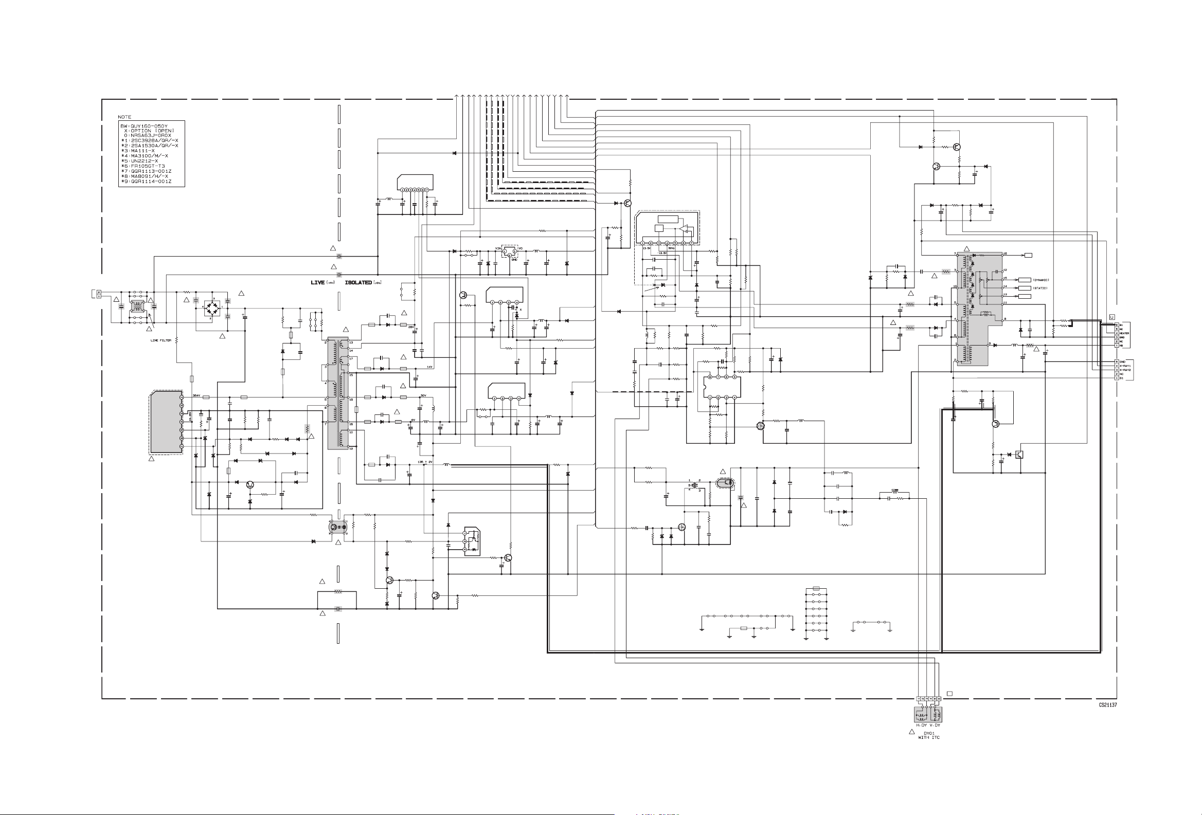
MAIN PWB CIRCUIT DIAGRAM [AV-29VT15/R] (2/2)
Y905
FRONT
CONTROL
PWB ASS'Y
CN00W
CN00W
QGA7901C1-02
X
Y906
X
!
QFZ9072-224
C901
Y907
Y908
!
X
!
X
QQR1356-001
!
QFZ9077-104
C902
LF902
IC921
STR-W6756-F5
S/GND
VCC
OLP
FB
OCP
D
NC
R901
QRF154K-2R2
!
R902
QRL039J-823
K901
*9
C903
QCZ9015-102Z
D933
MTZJ9.1C-T2
D901
GSIB460-S1
K923
BW
C922
C924
1/50
.1
1K
R929
D935
MTZJ9.1C-T2
D934
MTZJ9.1C-T2
D932
MTZJ36A-T2
!
C905
.001
AC400V
QCZ9015-102Z
QRL039J-473
C906
QEZ0649-337
!
C904
QCZ9015-102Z
K922
*7
C931
QCZ0364-102
R923
.47
C928
2W
1000P
R922
D927
*3
R921
R924
33K
D923
*3
D924
MA8330/M/-X
D925
Q921 D921
2SC3852A RGP10J-5025-T3
C921
22/50
D930
MA8240/M/-X
D928
100
1/2W MA8240/M/-X
K902
QQR1113-001Z
RGP10J-5025-T3
R930
47K
K921
*9
C926
QFLC1HJ-472Z
R934
QRZ0237-R18
1.8K
R933
10K
K924
BW
D926
RGP10M-5010-T3
D936
1SS133-T2
QCB32HK-181Z
C925
22/100
QCB32HK-103
1SS133-T21/2W
D929
C917
C929
.01/500
QCZ0325-391
D922
*3
C915
MA8062/M/-X
QCZ9079-471
QCZ9079-471
Y911
Y912
QUY160-100Y
R932
!
R935
1K
1/2W
D931
R991
QRZ9046-825Z
C993
QCZ9079-102
C991
C992
QUY160-100Y
QRZ9017-100
!
8.2M
!
.001
AC400V
!
!
X
FR901
T921
QQS0267-001
PC901
PS2581AL1/QW/
VER_PROTECT
VDRB-EWVDRA+
NECK
R791
QRE121J-102Y
L972
L973
QQL244J-5R6Z
C984
D977
*3
QQL26AK-820Z
C967
470/16
47/50
L975
C978
C981
100/16
R976
MA8082/M/-X
R962
QRL029J-223
STB1
STB
PROTECT
VER_PROTECT
STB1
EW
EW
VDRB-
VDRB-
VDRA+
VDRA+
NECK
NECK
ABL
ABL
HFB
HFB
PROTECT
3.3V_STB
P_ON/OFF
H_DRIVE
32V
12V
VER_PROTECT
5V
8V
PROTECT
3.3V_STB
STB1
A_VCC
3.3V_STB
D791
MA8062/M/-X
12V
D973
*3
PROTECT
390
P_ON/OFF
8V
D970
PROTECT
12V
D975
*3
5V
C968
470/16
32V
STB
D962
MA8330/M/-X
STB
A_VCC
P_ON/OFF
H_DRIVE
D472
*3
R471
1M
C471
10/50
1SR124-400A-T2
D471
NCF21HZ-334X
NCF21HZ-334X
R475
Q471
120K
R472
L421
QQL26AK-220Z
C435
C436
R448
1
1/2W
R520
470
X
X
C422
X
D422
QRL039J-121
QRL039J-121
R521
100K
MA8091/H/-X
Vcc -Vcc
C423
QCS32HJ-560Z
R437
X
QRG01GJ-331
QFLC2AJ-563Z
R524
R525
C523
47/35
C520
0
D524
V.OUT
IC401
LA78041
THERMAL
PROTECTION
PUMP
UP
.001
R438
1M
C424
QFLC2AJ-683Z
R439
X
1/2W
R440
C430
QRE121J-3R9Y
C451
X
H_DRIVE
BSN304-T
D520
V.OUT
AMP
R473
68K
6.8K
R474
R427
220K
C428
QEHR1VM-107Z
C420
X
D423
GP10DE-5009-T2
C427
1000/35
C431
.1
R434
6.8K
R435
C429
R430
4.7K
R431
X
1/2W
R433
C452
Q521
G
X
X
X
R451
X
R452
C454
0
X
R455
330
R432
QRX01GJ-1R2
IC451
X
R458
0
X
QQR1229-001
R470
R462
0
0
R463
X
R461
X
Q522
T521
D
C521
.0033
S
!
TT2142-YD
R522
22
1/2W
270
R523
QRL029J-271
C522
MY
.022
QFLC1HJ-223Z
Y982 Y980 Y979 Y978 Y974
QUY160-100Y QUY160-200Y QUY160-125Y QQR1114-001Z
GND GND
4.7K
R426
X
R454
X
R453
R456
X
QUY160-100Y
R411
4.7K
RDN050N20
C524
QFZ0196-202
!
BW
K102
Q461
4.7K
R412
R457
X
R459
X
R460
82K
1/2W
G
QUY160-125Y
GNDGND
C453
D
S
C526
QFZ0196-252
Y975
X
R464
QRL039J-330
D522
RU4AM-LFT2
D521
D451
RH3G-F1
X
L521
QQLZ036-821
C531
QEZ0195-475Z
C525
QFZ0196-123
C528
.022
QFP32JJ-223
400V
C542
X
C529
QENC2AM-225Z
QUY160-075Y
GNDGND
C527
QFZ0197-204
C582
QFZ0197-204
QRL039J-393
K105
QUY160-150Y
Y961
QUY160-125Y
Y976
QUY160-200Y
Y983
BW
Y971
X
Y915
BW
Y984
D554
MA8051/L/-X
L523
X
D523
*6
R527
Y914 Y913
X
GND GND
R555
X
C530
QCB32HK-561Z
QUY160-125Y
C556
R554
1.8K
!
L522
QQR1243-001
X
R551
QRZ9021-1R0
QEHR1EM-108Z
R552
QRZ9021-1R0
C554
QEHR1EM-108Z
R528
470
1/2W
D555
X
!
C553
FR
D594
X
C555
QFLC2AJ-103Z
MY
1
Q591
X
R591
X
QCB32HK-561Z
QCB32HK-561Z
R597
D591
X
C591
X
R533
!
QRZ9017-4R7
C551
D551
*6
D552
*6
C552
QRZ0225-2R2
X
Q592
X
R596
X
R595
D593
X
X
C593R594
XX
R592
D592
X
X
4.7
R572
QRA14CF-1202Y
R571
C571
220/160
QETM2CM-227
!
100/16
C572
T522
QQH0184-001
C592R593
XX
FBT
D530
*6
R574
18K
1/2W
R575
2.2K
QQL244K-220Z
R573
3.3K
Q571
2SA1208/ST/Z1-T
D571
MA8075/H/-X
C573
47/25
EHT
FOCUS2
FOCUS1
SCREEN
R582
82K
1/2W
R583
C532
10/250
180K
R581
1/2W
8.2K
1/2W
D581
C581
.1
*6
L530
R530
QRZ9017-4R7
!
C580
X
Q572
*5
CN00U
QJK002-063231
CRT SOCKET
PWB ASS'Y
CN00U
CN00X
QGA2501F1-05
ADJUSTMENT
CONNECTOR
HFB
ABL
3.3V
3.3V_STB
A_GND
A_VCC8V5V
BL_GND
D976
SUB
VIN
C963
.001
C958
L952
QQL26AK-820Z
R971
X
C971
X
D972
1SR124-400A-T2
L954
QQL244J-5R6Z
C949
2200/10
L951
QQLZ026-480
D958
QUY160-100Y
C950
.1
Q952
*1
X
D961
X
Y972
QUY160-075Y
2SA1013/RO/-T
R958
18K
R972
X
C975
470/10
D974
X
Q958
R960
22K
1/2W
C979
4.7/50
R977
X
BW
Y977
C989
.1
IC951
SE135N
22/50
R959
15K
IC971
X
VONCGNDCNCONT
L971
X
C974
C973
X
X
C972
X
R965
Y965
X
BW
C955
QCB32HK-222Z
FMX-G12S
C953
QCB32HK-222Z
D953
*6
C954
QCB32HK-222Z
D954
*6
C952
D952
FMX-G12S
QCZ0364-122
RU4AM-LFT2
C951
R950
X
Q951
*1
R956
0
!
CP955
ICP-N75-Y
CP
D955
C960
2200/35
C962
0
!
CP953K953
ICP-N38-Y
CP
330/25
!
CP954
ICP-N38-Y
CP
C959
330/35
!
CP952
ICP-N38-Y
CP
C957
2200/10
C964
100/35
C940
D951
C956
QEZ0203-227
R953
3.3K
1/2W
R954
D959
D960
3.3K
1/2W
0
0
R955
0
C969
R957
X 15K
K955
*7
!
*7
K954
*7
K957
QCB32HK-222Z
X
K952
*9
K951
*9
QCZ0364-561
R951
1K
1/2W
R952
X
1/2W
!
D957
MA8039/H/-X
12V
C976
4700p
PQ120RDA1SZ
VINVOGND
R970
1.8K
1/2W
PQ050RDA1SZ
VINVOGND
R980
5.6K
C945
32V
IC972
BA33BC0T
IC973
C961
IC975
R973
10K
X
H_DRIVE
PROTECT
P_ON/OFF
CONT
C994
C987
1/50
R975
2.2K
Q957
*1
D971
100/16
CONT
*3
C980
QQL244J-5R6Z
C977
47/50
47/50
R981
10K
MAIN PWB ASS'Y (2/2)
SCW-1132A-H2 [AV-29VT15/R]
Note: 1. Refer to page 2-23 for voltages of this circuit diagram.
2. Refer to page 2-24 for waveforms of this circuit diagram.
CN0HV
QGZ5003C1-06
HV
!
DEF YOKE
2-8(No.YA256)(No.YA256)2-7
Page 85

MAIN PWB CIRCUIT DIAGRAM [AV-29VT35/R] (1/2)
D706
C777
.1
VCCWPSCL
IC702
A0A1A2
IC974
!
MM1561JF-X
C965C983
10/50
C110
.1
R107
X
D101
X
X
0
R109
Y007
X
X
Q102
Y004
X
Q103
X
X
C108
Q001
X
DGS
Y005
0
Y006
0
BL_GND
3.3V_STB
A_VCC
A_GND
H_DRIVE
P_ON/OFF
VDRA+
VDRB-
PROTECT
VER_PROTECT
MA8036-X
IC976
MM1561JF-X
R978
Y981
3.3K
X
C986
C985
47/16 .1
STB1
8V
5V
12V
3.3V
NECK
HFB
ABL
EW
32V
TU001
QAU0353-001
TUNER
X
L001
K103
R101
0
R001
220
L002
C005
.0022
R005
82
CF101
QAX0349-001
C001
.01
QQL244J-4R7Z
C003
.1
R002
220
QQL244K-8R2Z
C002
10/50
C004
470/16
33/16
C006
R003
IF
NC
32V
LOCK
5V
BM
SDA
SCL
AS
BT
AGC
R004
27K
Y973
X
x
K101
C101
.01
3.9K
X
R008
L003
QQL244J-4R7Z
8.2K1.8K
R102R103
.01
C103
X
R007
QQL244K-1R0Z
100
R104
22
R105
47/25
C104
R006
X
Q002
C111
470/16
L101
C109
Q101
2SC5083/L-P/-T
27
R106
R108
.01
C102
X
D001
DGS
X
MAIN PWB ASS'Y (1/2)
SCW-1133A-H2 [AV-29VT35/R]
QGA2501C5-06Z
SDA
VSS
.1
X
R110
X
19
18
CN002
0
Y709
Y_GND
Y_GND
V3
SDA1
SCL1
*4
L713
.22
3.3K
3.3K
10K
C768
R745
R743
R784
100
R742
R744
SDA1
SCL1
V3.3P
Audio2InL
.1
C736
C744
.01
.1
C745
*8
D702
C735
0
Y707
V3
Y728
QQR1114-001Z
GND GND
Y814 Y813
XBW
FRONT CONTROL
PWB ASS'Y
CN002
16
X
Y708
L3
GND_INR3KEYIN
220
R741
POWER
Audio2InR
D703
C737
75
15
14
13
10K
R785
BASS_ON/OFF
V2/YL2R2
X
CH
.1
R716
8.2K
L2
V2/Y
GND
12
*3
D711
S_REDUCE
1
C738
10K
R717
11
12V
*3
D712
VER_PROTECT
CH
C739
10K
8.2K
R718
R719
R2
9 8 7 6 5 4 3 2 1
10
ROTATION
W-L1
1
.1
C740
Y1/CVBS1
17
PW
100
.1
R739
B_MUTE
L_AOUT
A_GND
1.8V
VER_PROTECT
W-B1
.22
C767
VssC2
COMPONANT-PIP
COMB_SW_NT3.5/OTHER
Y3/CvbsC1AudOutLsL
D710
*8
.1
*8
C741
D704
C742
0
Y710
100
R768
C743
10/50 10/50
C1
C1_GND
A_GND
A_VCC
R_AOUT
L712
V1.8C2
AudOutLsR
R720
1.5K
X
R769
HP_L
*4
PW_LED
HP_L
PW_LED
X
1.5K
R797
R721
X
R770
HP_R
P_ON/OFF
REMOTE
100
R736
PW_LED
V1.8ADC
V3.3RefAdP
Uout/INSSW2
Yin/G2/Y
Uin/B2/Pb
Vin/R2/Pr
VssComb
HP_R
X
R798
CVBSO/PIP
8V
B_MUTE
REMOTE
VssADC
V3.3A2
V1.8A
GndA
RefAd
RefAdN
V3.3A1
Bout
Gout
Rout
BLKIN
BCL
V5P3
Gnd3
B3/Pb
G3/Y
R3/Pr
INSSW3
Yout
Ysync
V5Comb
Hout
FbiSo
CVBSO/PIP
LC701
Y702
0
12V
C766
.22
C764
.1
C763
C761
C758
.22
C779
10/50
C752
C751
NC
C746
X
Y703
0
X
Y724
CVBSO/PIP_GND
A_MUTE
Y601
X
Y602
X
CP650
!
ICP-N50-Y
CRT SOCKET
PWB ASS'Y
CN00T
CN00T
QJK002-083633
12V
*3
V1.8A
L711
*4
C765
100/16
L710
*4
L709
.22
*4
C762
.1
100/16
L708
*4
C760
L707
.22
*4
C759
100/16
R735
R734
100
100
R733
100
C757
R732
560p
1k
R731
CH
1k
L706
D708
C756
.1
C753
.1
R730
150
.1
.1
R782
1.2K
R729
X
C780
.1
C750
.1
C749
.1
C748
.1
.1
27K
R726
1K
R724
X
R778
R722
Y_GND
R630
R631
D603
*3
C607
220/16
C608
220/16
*4
*3
C755
10/50
C754
.1
Y705
0
Y706
0
C747
10/50
L716
*4
100
R728
10k
R727
47
R725
*1
Q702
R723
470
470
5V
3.3K
R629
3.3K
3.3K
D601
*3
D607
*3
Q601
*2
R608
X
R609
27K
R616
X
D341
D342
*3
D343
*3
R310
X
Q306
R313
X
X
R314
C343
X
X
QUY160-100Y
K701
QUY160-150Y
ABL
H_DRIVE
HFB
OFF_MUTE
R617
10K
2.2K
R601
10K
R662
2.2K
R602
1K
R603
R611
8.2K
Q602
*2
C610
R610C609
100K33/50
R623 R620
33K 10K
Q607
R622
*1
10K
R341
0
R342
X
C302
X
R307
C303
X
R308
X
R309
X
X
R311
R312
Q305
X
C304
X
C305
Y715
Y301
X
K301
X
ANALOG
DIGITAL
NCNCNCNCNCNCNC
RIN
BINRFGND
10K
C601
C656
R618
10/50
100/50
C655
10/50
R612
100K
R613
R614
X
100K
Q603
Q604
UN2226-X
UN2226-X
R621
2.2K
Q608
*1
C613R624
10/5068K
Q341
*2
D344
X
R343
0
C341
220/16
X301
X
IC301
X
X
C342
X
X
X
C306
X
C307
X
C308
X
Y716
0
AUDIO AMP
IC601
AN7585
LINNCB_MUTE
L_OUT
L_R_MUTE
D602
*3
C602
10/50
.22.222.2
C603C604R606
8.2K
10K
R605
R604
R619R615
8.2K
Y603
QUY160-075Y
100K
100K
Q605
Q606
UN2226-X
UN2226-X
D608
D609
*3 *3
C617
4.7/50
R344
R345
0
R320 R321
XX
C316
X
C315
X
C314
X
C313
X
C312
X
C311
X
C310
X
C309
X
0
0
R315
R316
L301
X
L_AOUT
NC
STB
ROUT
C605
.22
C606
.22
R607
2.2
1/2W
270
R626
*5
Q609
0
R317
D604
R319
X
Q307
X
R_AOUT
C614
QETM1VM-228
D605
MA8300/H/-X
MA8300/H/-X
270
R627
*5
Q610
Y303
BASS
BW
Y302
L303
L302
X
X
X
D606
R318
W-B
MA8300/H/-X
0
D345
*3
GND_B
VCC
B_OUT
.22 .22
C612 C611
1/2W
2.2
R625
1/2W
X
CVBSO/PIP_GND
R632
1K
270
R628
*5
Q611
CVBSO/PIP
C661
L304
X
C317
X
3.3V
NECK
PB_GND
V2/Y_GND
PR_GND
W-L
220/16
12V
SCL1
SDA1
V2/Y
5V
5V
PB
PR
OFF_MUTE
C1_GND
C1
S_V_DET
Y1/CVBS1
Y_GND
VDO_DET
L1
R1
GND
BASS
A_GND
V2/Y
V2/Y_GND
PB
PB_GND
PR
PR_GND
L2
R2
5V
V_OUT
L_OUT
R_OUT
GND GND
QQR1199-001
R809
0
C809
X
Y009
QUY160-100Y
Y010
QUY160-150Y
Y604
BW
Y711
BW
Y719
0
Y720
QUY160-125Y
Y721
X
Y722
0
LC801
NCB21HK-152X
QQR1199-001
LC803
QQR1199-001
D753
*8
QQR1199-001
NCB21HK-152X
R808
X
KTA1267/YG/-T
Y801
Y802
D814
*8
R802
0
D801
R803
0
Y803
LC802
Y804
Y805
Y806
Y807
LC804
D803
Q801
Q805
*2
GND
R816
75
Y819
R801
75XX
BW
D815
*8
Y818
0
D802
NCB21HK-152X
D810
R804
X
*8
150
D751
Y816
X
*8
0
X
R805
75
D811
X
*8
X
R806
Y817
0
D804
NCB21HK-152X
R807
100
1/2W
C802
10/50
C803
10/50
Q803
Y725
GND
D812
*8
C804
470/16
D813
*8
R811
390
R810
R812
390
100K
R814
X
Y815
X
K601
QUY160-150Y
K702
QQR1113-001Z
K107
QQR1114-001Z
Y717
QUY160-075Y
Y712
0
Y713
0
Y714
BW
Y718
0
75
R815
75
QNN0349-001
82K
R813
82K
Q804
J804
UN2226-X
Y808
X
D805
XX
D806
UN2226-X
S1
J801
QNZ0454-002
V1
L1
R1
J805
QNS0100-001
J802
J802
QNN0349-002
QNN0349-002
J803
QNN0348-001
VIDEO-1
S-VIDEO
INPUT
BASS SPEAKER
OUT
VIDEO-2
COMPONENT
VIDEO
INPUT
OUTPUT
FRONT CONTROL
PWB ASS'Y
CN001
9 8 7 6 5 4 3 2 1
CN00C
220
220
220
220
R762
R763
R764
R765
PROT
5V
SDA1
SCL1
C778
47/16
R760
100
R761
C982
47/16
QAX0723-001
C106
.01
Y008
0
C107
X
Y003
X
X
C105
V1.8A
SCL0
100
SDA0
R974
1K
STB1
Q791
DTC124ESA-T
Y791
X
PW
P_ON/OFF
R737
3.3K
CONT
1.8V
R738
W-A2
10K
X
Q704
*1
D713
STB1
8V
A_VCC
A_GND
5V
12V
3.3V
NECK
H_DRIVE
HFB
ABL
EW
P_ON/OFF
VDRA+
VDRB-
PROTECT
VER_PROTECT
4.5/OTHER
3.58/OTHER
SF102
SF101
X
SDA1
SCL1
1.8V
VDRB-
VDRA+
5V
R796
0
SCL0
SDA0
L703
5V
NECK
CONT
EW
R781
4.7K
D707
*3
Q708
*2
R795 Q707
100K *1
R790
L701
*4
L702
*4
*4
R792
X
470/16
C703
L717
*4
C707
.1
C708
100/16
C713
C714
C715
R703
C716
R794
2.2K
C792
.1
1K
C706
3p
GND
C711
2.2/50
.001
C717
.047
K104
QUY160-150Y
W-C2
.1
C704
C705
3p
C709
.01
10/50
.022
.001
100
R704
/16
C719
R706
220
R707
56K
R708
100K
R779
Q703
10K
*2
R780
C789
100K
47/50
X
C791
Q705
SSM3K02F-X
15K
R783
R759
100
R793
W-C1
W-A1
VssP2
VssC4
C701
.22
V1.8C4
C702
.22
V3.3A3
VrefP_Sdac
CH
VrefN_Sdac
27p
VrefP_Sdac
C790
VrefN_Sdac
VrefP_Sdac
XtalIn
CH
XtalOut
CH
X701
VssA1
R756
100
NECK
CONT
C785
.22
V5P1
Ph2
R701C710
12K6800p
Ph1
Gnd1
C712
.22
SecPll
Dec8G
100
R702
EW
VDRB-
VDRA+
100
Vif1
Vif2
Vsc
C718
.1
Iref
R705
39K
GndIF
Sif1
Sif2
.01
AGC
C720
.001
EHT SVM
R709
C721
1M
x
D701
*3
R710
ABL
12V
CF702
L651
QQL244J-4R7Z
R651
1.2K
D651
MA8062/M/-X
1.8V
PROTECT
Q706
SSM3K02F-X
D
G
S
D
G
S
*4
.22
C775
L715
4.7K
R757
3.3K
R758
3.3k
.1
C776
SCLO
SDAO
VssC3
V1.8C3
P12/Int2
L3R3L_OUT
Ssif/RefIn/Avl/RefOut
x
x
R652
R_OUT
1
1
C723
C724
R711
8.2K
L3
X
QUY160-100Y
GND GND GND
.1
C725
10K
10K
8.2K
R713
R712
R714
R3
R_OUT
L_OUT
X
CF701
x
R653
0
R654
0
C651
47/16
Y012 Y011 Y726 Y727 Y723
BW X X X
CN001
MA8039/H/-X
D705
P25/PWM4
S_V_DET
100
R777
S_V_DET
C783
QGF1220C2-09
R755
1.2K
R740
15K
R776
D709
1/50
VssC1+P1
VDO_DET
15K
*3
R754
VDO_DET
12V
ECO_IN
1.8V
KEYIN
ECO_IN
R753
1.2K
.1
0
.22
2.2/50
L714
C774
C772
C773
0
Y704
220
100
R752
V1.8C1
ECO_IN
KEY_IN
DecV1V8
1K
R751
PW_LED
PROT
X
D714
C771
PROT
REMOTE
A_MUTE
4.5/OTHER
MA8030/H/-X
X.1
R750 C770
1K
R749
4.5/OTHER
A_MUTE
5V
100
R747
IC701
QGF1220C2-19
3.58/OTHER
.1
2.7K
R748
C769
1K
10k
R771
3.58/OTHER
ROTATION
R746
ROTATION
MAIN MICRO COMPUTER/
IF㨯VIDEO㨯RGB㨯SYNC㨯DEF.PROCESS
DecsDem
QssO/AmO/AudeEm
Gnd2
PllIf
SifAgc
IfVo/FmRo/DvbONCV8AudioSwitches
AgcSsif
V5P2
V_OUTL1R1V3C4
1
390
3300p
R715
C727
C729
.1
C728
10/50
C726
Q701
x
C722Y701
x
R663
22K
R664
IC651
RC4558D-X
R655
22K
C652
R656
100p
33K
CH
2.2/50
C732
2.2/50
.1
*4
220/50
X
C731
L704
C730
C786
8V
R766
x
R767
x
C657
10/50
NN
C658
10/50
22K
C659
X
R658R657 R659
22K33K 20K
R660
39K 22K
C660
.47
NCF31CZ-474X
GND GND
1
C781
C782
.1
10K
10K
8.2K
8.2K
10/50
*4
C734
R774
R775
R773
R772
C733
L705
R1
5V
L1
V_OUT
5V
HP_R
HP_L
IC651
RC4558D-X
C654
10/50
C653
.01
R661
Note: 1. Refer to part list for the part number of IC701 and IC702.
ޓޓ 2. Refer to page 2-23 for voltages of this circuit diagram.
3. Refer to page 2-24 for waveforms of this circuit diagram.
(No.YA256)2-9 2-10(No.YA256)
Page 86

MAIN PWB CIRCUIT DIAGRAM [AV-29VT35/R] (2/2)
X
FRONT
CONTROL
PWB ASS'Y
CN00W
CN00W
QGA7901C1-02
Y905
X
Y906
!
QFZ9072-224
C901
X
Y907
X
Y908
!
LF902
QQR1356-001
STR-W6756-F5
QFZ9077-104
C902
!
IC921
S/GND
NC
VCC
OLP
FB
OCP
QRF154K-2R2
D
R901
!
R902
QRL039J-823
K901
*9
D933
C903
QCZ9015-102Z
C922
.1
R929
MTZJ9.1C-T2
1K
GSIB460-S1
K923
BW
D901
C905
!
QCZ9015-102Z
!
C904
QCZ9015-102Z
K922
C924
C931
QCZ0364-102
1/50
C928
1000P
D935
R921
MTZJ9.1C-T2
100
1/2W MA8240/M/-X
D923
MTZJ9.1C-T2
D932
MTZJ36A-T2
*3
K902
QQR1113-001Z
D925
*6
C921
22/50
D934
.001
AC400V
C906
QEZ0649-337
*7
R923
.47
2W
D927
*3
R924
33K
D924
MA8330/M/-X
Q921 D921
2SC3852A
D930
MA8240/M/-X
QRL039J-473
R922
QRZ0237-R18
D928
R933
R930
47K
K921
*9
C926
QFLC1HJ-472Z
R934
1.8K
10K
K924
BW
D926
RGP10M-5010-T3
D936
1SS133-T2
QCB32HK-181Z
C925
22/100
QCB32HK-103
1SS133-T21/2W
D929
C917
C929
.01/500
QCZ0325-391
D922
*3
*6
Y912
C915
D931
MA8062/M/-X
!
QCZ9079-471
!
QCZ9079-471
Y911
QUY160-100Y
QUY160-100Y
!
R932
QRZ9017-100
R935
1K
1/2W
QRZ9046-825Z
C993
.001
QCZ9079-102
C991
C992
R991
8.2M
AC400V
X
FR901
!
T921
QQS0267-001
PC901
PS2581AL1/QW/
!
!
VER_PROTECT
VDRB-EWVDRA+
NECK
R791
QRE121J-102Y
L972
L973
QQL244J-5R6Z
C984
D977
*3
QQL26AK-820Z
C967
470/16
47/50
L975
C978
C981
100/16
R976
MA8082/M/-X
R962
QRL029J-223
390
STB1
470/16
D973
*3
D970
C968
VER_PROTECT
3.3V_STB
D791
MA8062/M/-X
P_ON/OFF
D975
*3
D962
MA8330/M/-X
PROTECT
P_ON/OFF
H_DRIVE
3.3V_STB
A_VCC
PROTECT
PROTECT
P_ON/OFF
STB1
A_VCC
STB1
VDRB-
VDRA+
NECK
STB
PROTECT
EW
EW
VDRB-
VDRA+
NECK
ABL
ABL
HFB
HFB
3.3V_STB
D472
*3
R471
1M
C471
10/50
D471
1SR124-400A-T2
NCF21HZ-334X
NCF21HZ-334X
R472
120K
QQL26AK-220Z
C435
C436
R448
1
1/2W
R520
470
R475
X
Q471
X
L421
C423
C422
QCS32HJ-560Z
R437
QFLC2AJ-563Z
R524
QRL039J-121
R525
QRL039J-121
C520
0
R521
100K
MA8091/H/-X
PUMP
UP
Vcc -Vcc
.001
X
QFLC2AJ-683Z
R439
1/2W
R440
QRG01GJ-331
C430
C451
C523
47/35
D524
V.OUT
IC401
AN15526A
V.OUT
THERMAL
PROTECTION
D422
X
R438
1M
C424
X
R433
QRE121J-3R9Y
X
Q521
H_DRIVE
BSN304-T
D520
X
AMP
QEHR1VM-107Z
GP10DE-5009-T2
C431
.1
R430
C429
X
4.7K
R431
X
1/2W
R432
QRX01GJ-1R2
C452
22/50
T521
QQR1229-001
D
C521
G
.0033
S
6.8K
R473
68K
R427
R474
220K
C428
C420
X
D423
C427
1000/35
6.8K
R434
R435
X
R451
680
1/2W
C454
R452
X
2.7K
R455
12K
IC451
UPC358G2-XE
R458
33K
R470
R462
X
1.2K
R463
R461
1K
5.6K
Q522
!
TT2142-YD
R522
22
1/2W
270
R523
QRL029J-271
C522
MY
.022
QFLC1HJ-223Z
Y982 Y980 Y979 Y978 Y974
QUY160-100Y QUY160-200Y QUY160-125Y QUY160-150Y
GND GND
QUY160-100Y
4.7K
R411
4.7K
R426
R453
22K
R454
5.6K
R456
5.6K
2SD1267A/QP/
!
BW
K102
Q461
C524
QFZ0196-202
R412
4.7K
R457
82K
R459
8.2K
R460
22K
1/2W
QUY160-125Y
GNDGND
C526
QFZ0196-252
Y975
C453
10/50
R464
QRL039J-330
D522
31DF6N-FC5
D451
MA8043/L/-X
D521
RH3G-F1
QQR1138-001
C531
4.7/250
QEZ0195-475Z
C525
QFZ0196-123
C528
.022
QFP32JJ-223
C556
X
D555
X
R554
R555
X
X
C530
QCB32HK-561Z
QUY160-125Y
1.8K
!
L522
QQR1243-001
R551
!
1
QRZ9021-1R0
QEHR1EM-108Z
R552
QRZ9021-1R0
R528
470
1/2W
D554
MA8051/L/-X
L521
400V
C542
X
QENC2AM-225Z
QFZ0197-204
C529
K105
QUY160-150Y
Y961
X
Y976
QUY160-200Y
Y983
BW
Y971
X
Y915
BW
Y984
QUY160-075Y
GNDGND
C582
R527
QRL039J-393
GND GND
L523
X
C527
QFZ0197-204
D523
*6
Y914 Y913
32V
12V
VER_PROTECT
5V
8V
PROTECT
12V
8V
12V
5V
32V
STB
STB
H_DRIVE
FR
C553
FR
QCB32HK-561Z
C554
QEHR1EM-108Z
D594
X
Q591
X
R591
C555
QFLC2AJ-103Z
MY
QCB32HK-561Z
C552
D591
C591
X
X
X
QRZ9017-4R7
C551
D551
*6
D552
*6
R597
X
Q592
X
R596
X
R595
D593
X
X
C593R594
XX
R592
D592
X
X
!
R533
4.7
R572
QRA14CF-1202Y
R571
QRZ0225-2R2
C571
220/160
QETM2CM-227
!
QQH0184-001
C572
100/16
C592R593
XX
FBT
T522
D530
EU2-T3
R574
18K
1/2W
R575
2.2K
QQL244K-220Z
R573
3.3K
Q571
2SA1208/ST/Z1-T
D571
MA8075/H/-X
C573
47/25
EHT
FOCUS2
FOCUS1
SCREEN
R582
82K
1/2W
R583
10/250
180K
1/2W
R581
1/2W
8.2K
C532
D581
C581
.1
*6
L530
R530
QRZ9017-4R7
!
C580
X
Q572
*5
CN00U
QJK002-063231
CRT SOCKET
PWB ASS'Y
CN00U
CN00X
QGA2501F1-05
ADJUSTMENT
CONNECTOR
HFB
ABL
P_ON/OFF
3.3V
3.3V_STB
A_GND
A_VCC8V5V
BL_GND
D976
SUB
VIN
C963
.001
L952
QQL26AK-820Z
R971
X
C971
X
D972
1SR124-400A-T2
L954
QQL244J-5R6Z
C949
2200/10
L951
QQLZ026-480
D958
QUY160-100Y
C950
.1
Q952
*1
X
D961
X
Y972
QUY160-075Y
2SA1013/RO/-T
R958
18K
R972
X
C975
470/10
D974
X
Q958
R960
22K
1/2W
C979
4.7/50
R977
X
BW
Y977
C989
.1
IC951
SE135N
22/50
R959
15K
IC971
X
VONCGNDCNCONT
L971
X
C974
C973
X
X
C972
X
Y965
X
R965
QRT039J-R47
C955
QCB32HK-222Z
FSF05A20
C953
QCB32HK-222Z
D953
*6
C954
QCB32HK-222Z
D954
*6
C952
D952
FSF05A20
QCZ0364-122
31DF6N-FC5
C951
R950
X
Q951
*1
R956
0
!
CP955
ICP-N75-Y
CP
D955
C960
2200/35
C962
0
!
CP953K953
ICP-N38-Y
CP
C958
330/25
!
CP954
ICP-N38-Y
CP
C959
330/35
!
CP952
ICP-N38-Y
CP
C957
2200/10
C964
100/35
C940
D951
C956
QEZ0203-227
R953
3.3K
1/2W
R954
D959
D960
3.3K
1/2W
0
0
R955
0
C969
R957
X 15K
K955
*7
*7
K954
*7
K957
X
QCB32HK-222Z
K952
*9
K951
*9
QCZ0364-561
R951
1K
1/2W
R952
X
1/2W
!
D957
MA8039/H/-X
12V
BA33BC0T
C976
4700p
PQ120RDA1SZ
VINVOGND
R970
1.8K
1/2W
PQ050RDA1SZ
VINVOGND
R980
5.6K
C945
PROTECT
32V
H_DRIVE
IC972
QQL244J-5R6Z
C977
47/50
IC973
CONT
C994
D971
*3
C980
100/16
R973
10K
C961
47/50
X
IC975
CONT
C987
1/50
R981
10K
R975
2.2K
Q957
*1
MAIN PWB ASS'Y (2/2)
SCW-1133A-H2 [AV-29VT35/R]
Note: 1. Refer to page 2-23 for voltages of this circuit diagram.
2. Refer to page 2-24 for waveforms of this circuit diagram.
HV
CN0HV
QGZ5003C1-06
!
DEF YOKE
2-12(No.YA256)(No.YA256)2-11
Page 87

CRT SOCKET PWB CIRCUIT DIAGRAM
CN00T
QGA2501C5-08Z
MAIN PWB
ASS'Y(1/2)
CN00T
CRT SOCKET PWB ASS'Y
SCW-3020A-H2
D363
X
100
R351
R352
100
R353
100
R354
D350
MA8075/M/-X
CN0E1
100
Q373
R350
X
IC351
TDA6107AJF/N1
C351
1000p
CH
C352
4.7/250
QRC121K-561Z
C353
QFKC2EK-104Z
D357
EU01N-T2
L351
QQL244J-5R6Z
Q371
X
Q372
X
X
D371
X
CN0E2
R371
X
R372
R373
X
Q374
X
X
QRC121K-561Z
R355
R356
EU01N-T2
EU01N-T2
D354
D355
R375
X
R376
X
QRZ0107-152Z
QRC121K-561Z
R359
1.5K
R357
QRZ0107-152Z
TP-47G
R360
1.5K
QRZ0107-152Z
EU01N-T2
D356
R377
X
C371
X
D372
X
R358
1.5K
SG352
X
SG351
X
C360
TP-E
X
TP-47B
SG353
TP-47R
!
R369
QRZ9023-1R2
!
SK351
QNZ0536-001
X
!
SK351
QNZ0536-001
SG354
X
C358
X
C359
.0022
!
R374
470K
QRZ0107-474Z
CN0SC
QGZ0017C1-01Z
QGA2501C5-06Z
MAIN PWB
ASS'Y(2/2)
CN00U
CN00U
HB
GNDH
HEATER
C201
220/16
K207
QUY160-150Y
R201 R204
XX
C202
R202
X
N
R203
HB
GNDH
R221
1.2K
R222
56K
1/2W
R223
56K
1/2W
R224
1.2K
HEATER
R227
2.7
1/2W
R225
39
R226
2.7
1/2W
Q208
2SA2140/QP/
K203
QQR1114-001Z
Q209
2SC5993/QP/
R228
39
R229
QRE121J-121Y
C217
100/10
D203
RGP10J-5025-T3
R232
390
QRL029J-391
K205
QQR1114-001Z
K204
QUY160-150Y
D204
RGP10J-5025-T3
C218
100/10
C219
330/10
OMR
WJM0048-002A
C220
QCS32HJ-680Z
CN0VM
GNDH
*3
*3
K202
QQR1114-001Z
Q203
*6
R212
150
R213
220
K201
QQR1114-001Z
C207
5p
QCS31HJ-5R0Z
R211
C205
560p
C206
3.3/50
1.5K
D201
D202
Q202
Q201
X
X
R205
X
X
R206
X
R207
0
C203
X
10/50
R208
15K
R209
1.5K
C204
R210
NDC31HJ-471X
2.7K
R214
10
1/4W
GNDH
K206
Q204
*6
Q206
*7
QQR1114-001Z
Q205
X
R216
X
Q207
X
R215
X
C208
C210
X
R217
X
R218
560
FR201
!
QRZ9021-561
C209
100/16
K208
Y353
X
R219
47
X
X
Y354
R220
47
X
QCB32HK-472Z
C216
10/160
C215
.0047
QQR1113-001Z
C214
10/160
C213
1000p
C212
C211
820p
CH
GNDH
(No.YA256)2-13 2-14(No.YA256)
Page 88

A
FRONT CONTROL PWB CIRCUIT DIAGRAM
L01
!
ROTATION COIL
CN00R
QGA2501C5-03Z
VIDEO-3
INPUT
J804
R3 L3 V3
J803
QNN0279-002 QNN0279-003QNN0657-001
J802
J801
QNS0155-001
D805
NCB21HK-152X
K402
QUY160-100Y
C489
560p
CH
R494
68K
R493
X
R807
X
BL_GND
12V
ROTATION
C490
22/50
M_GND
R806
0
AUDIO_R
QSW0619-003Z
QSW0619-003Z
QSW0619-003Z
M_GND
KEYIN
K403
QQR1114-001Z
R808
X
S803
S802
S801
QSW0619-003Z
S806
QSW0619-003Z
S805
QSW0619-003Z
S804
X
Y804
R809
0
A_GND
MAIN PWB
ASS'Y (2/2)
CN00W
!
QGZ5004C1-02
DEG COIL
CN0PW
QGA7901C1-02
!
C110V-AC240V
50Hz/60Hz
CN00W
WJK0200-008A-E
CNDEG
QSW0750-001
!
TH901
QAD0145-2R3
Y901
!
S901
QFZ9072-224
LF901
QQR1356-001
X
X
Y902
!
QFZ9072-224
QRZ0107-474Z
!
F901
QMF51E2-4R0J4
!
C902
!
C901
!
R901
VA901
!
QAF0060-621
Y903
X
!
QSK0061-002
X
Y904
RY901
Q955
*1
D956
*3
R960
22K
R961
47K
D957
R499
QRE121J-561Y
C487
QFLC1HJ-103Z
C965
100/16
IC481
LA6515
*3
R491
0
L401
QQL244K-820Z
.22
C483
NCB31CK-224X
C485
47/16
C484
.22
NCB31CK-224X
K401
QQR1114-001Z
R496
22K
Q481
*1
R495
1.5K
R492
10K
D491
X
R801
1K
R803
470
D801
IC801
RPM7238-H5
C802
100/16
C801
.1
R802
47
LH22440-T16
POWER_LED( RED)
D802
R481
QUY153-050Y
C481
.22
IC301
S9066-11
R301
0
X
R302
R305
0
R306
X
D301
X
R303
330K
x
R304
0
C301
1/50
Q301
X
R307
0
NCB31CK-224X
C482
.22
NCB31CK-224X
R483
68K
R484
6.8K
R482
120K
R486
R485
33K
5.6K
R487
3.3K
R488
150K
Q482
*2
R489
100K
R497
5.6K
C488
1/50
X
R490
9 8 7 6 5 4 3 2 1
MAIN PWB ASS'Y(1/2)
CN001
CN001
QGF1220C2-09
CN002
QGF1220C2-19
V_GND
AUDIO_L
A_GND
AUDIO_R
M_GND
123456789
MAIN PWB ASS'Y(1/2)
FRONT CONTROL PWB ASS'Y
D803Y802
MA8091/H/-X
D804
NCB21HK-152X
X
C803
C804
QUY153-050Y
X
Y801
X
12V
BL_GND
ROTATION
VIDEO
M_GND
AUDIO_L
KEYIN
101112131415161718
CN002
R811
0
R812
180
R813
220
R814
330
R815
470
R816
820
B_MUTE
R810
X
V_GND
L
LC801
QQR1199-001
X
Y803
R601
R602
R
QRE121J-271Y
1K
C601
1000/25
D601
X
SPEAKER
19
R604
1K
R603
LLRR
+- - +
QRE121J-271Y
C602
1000/25
D602
QGA2501C5-04Z
X
CN00S
SCW-8010A-H2
2-16(No.YA256)(No.YA256)2-15
Page 89

T
PATTERN DIAGRAMS
MAIN PWB PATTERN
B1
C522
Q521
C521
C523
HS522
Y708
Y709
R522
CN002
R523
T521
Q461
Q522
W216
R520
R521
C520
D520
D524
C524
C526
W193
W048
W087
R464
Y725
R456
R454
R453
R460
Y722
IC451
Y721
W174
C
R795
C792
R572
D7
C777
C424
W202
W025
E4
R978
Q707
D707
R796
R794
R791
91
Y981
R974
W175
Q791
Y791
R779
W032
R780
W194
Q703
W086
D706
C778
R737
C785
W004
W023
W120
C471
R435
R430
R426
C429
R412
R427
R434
IC401
C431
HS401
C427
W114
E5
R530
R762
R763
R764
R765
CN00C
C532
CN00U
R5
83
C581
W062
R581
C573
R
5
9
1
R597
D594
R596
Q592
D591
D593
D592
C591
R592
Q708
R573
W172
W204
R555
D554
Q591
C420
D708
R575
R574
W125
W211
R582
C592
W181
C789
R411
W098
W182
IC702
C572
W176
W185
D571
R593
W084
W123
W122
W095
W038
R554
C556
CN00X
W177
R781
R761
R755
R777
W124
W035
C106 C107
W002
R709
W203
Q571
R595
C593
R594
W113
R731
C571
R743
R745
R760
Y007
W192
L715
C775
R793
R757
R758
R759
D
W115
C111
W197
R962
C109
D701
Q572
W131
W034
W121
W054
W1
86
W173
W017
W091
W135
L703
R753
R776
R740
C7 03
W022
Y010
W163
W142
W042
C708
R702
Y003
D
L001
K101
R748
W102
W130
W170
R746
R784
W021
W158
W148
W147
R751
R752
R749
L714
71R7
C774
W136
R792
D709
R754
C
C776
W005
C704
C790
L702
R756
C7
07
C713
R703
R704
C105
D101
Q103
R103
R104
R107
R102
C101
W083
Y011
W141
W080
W082
L717
CF101
R708
W009
R005
C001
W079
D001
Q002
Q001
R007
Y005
W187
R001
Y006
R002
D962
C002
TU001
K103
C791
R527
W013
D552
C552
W033
D472
R439
C436
D423
D422
L421
C553
W057
D713
Q704
C435
C986
R471
A
Q471
R738
D551
C554
C965
R4 75
R552
W058
R448
W198
C551
R571
W201
D471
R437
C423
D555
IC976
Y973
W196
C428
C983
L530
C982
R473
C422
R551
W001
W028
IC974
C985
R474
R472
R438
C580
D581
D530
R462
R463
R470
R458
R461
R459
R452
R455
C454
C451
R457
C531
C542
C528
525
C
CN0HV
T522
521
D
R451
D451
C582
W019
D522
C527
L521
R533
L522
C452
W031
L523
R433
R431
R525
R524
C530
R528
C453
C529
D523
C430
C555
R432
W027
0
4
4
R
C711
R750
W143
W024
W076
W169
L713
W171
W1
W205
Q101
Y726
W077
W180
W179
R345
R342
D345
R343
R309
C308
C307
C306
R312
R344
L706
W139
R742
R744
R110
K105
C809
R003
K301
W166
Y716
L301
W160
Y303
W036
W190
C341
C7
55
L707
R7 36
L
12
L7
C767
IC701
R705
Y723
C718
Y008
Q102
Y004
C7 19
Y711
W220
R713
W047
R707
R711
C720
W043
W044
W046
W060
W045
W133
Y980
Y976
D813
K102
C802
W006
D806
R810
D805
Q803 Q804
C804
R815
R814
R811
C769
R7
47
W168
41R7
38
D7
05
L701
C702
C701
R701
C710
C714
C709
C716
L101
L003
R101
C005
W161
R785
D7
14
R7
C715
W078
W132
W178
Y302
W165
W164
Q341
D344
D341
D343
D342
R341
B
W137
L709
L711
D711
D712
W014
C7 63
L710
C7
68
W144
W011
C770
W146
Y7 04
C772
C771
W191
W217
Q705
C773
Q706
C7
A
83
83
R7
90
C705
X701
C706
C712
SF102
C717
Y727
SF101
R109
C103
C110
W110
C108
C104
C102
R108
R105
R106
Y012
R706
W075
R809
R808
Y982
Q801
R807
L002
Y009
C004
R006
C003
R008
C006
R004
K107
Y701
Q307
Y301
CF702
R813
66C7
W073
Y728
R310
Q306
65
W055
10R7
W003
CF701
Q805
L708
C7
R812
C803
R318
R321
R320
R319
W167
C315
C316
C312
C313
C314
C317
W088
R311
Q305
X301
R314
C3
02
C303
R313
C343
C761
C758
C760
35
R7
C759
C764
C762
R734
C732
C728
C726
W049
C7 25
21
C7
W039
C722
R767
R712
C724
C723
R714
Q701
W061
Y979
Q611
R626
R627
Q609
Q610
W053
W0
40
LC804
Y808
W212
Y807
D804
R806
D803
Y813
R7
74
R772
R766
R775
C7
R732
CN00T
C780
R715
R718
D753
Y817
CN001
L304
C310
L303
L302
C311
IC301
Y715
C3
05
W063
R3
07
R308
C342
57
W052
R316
R315
C750
C748
C749
C304
R782
R317
19
W2
R7
54
33
C7
W215
W051
W2
13
C747
W214
C7
56
W117
C779
C753
W094
C7
51
W218
C746
W068
W067
W064
C738
W070
W072
C745
Y705
C744
R632
C661
Y805
D811
R717
R628
LC803
R805
J802J803J804
W059
C736
W056
R730
C7
29
L704
C727
C734
C731
C739
C730
R719
W118
K104
R716
R630
R629
B
Y806
Y816
D812
W101
W119
W188
R804
LC802
D810
D751
Y803
Y804
W108
W020
LC801
Y815
Y801
R631
HS601
R802
D609
R612
R614
W208
C602
R618
R613
J801
Y978
Y975
F
W018
W066
C741
R602
D815
C309
R729
W065
C733
L
Q604
Q603
Y802
D801
W111
Y712
C786
Q605
R801
W189
R601
D608
W050
K701
W129
L651
E
R604
W1
C658
Y7
13
Y717
C617
Y714
L705
W107
W106
R662
D814
34
W104
W105
R816
W184
W085
W089
R654
C743
R773
C655
C6
C781
Y724
R7
W069
R617
51
W037
22
C782
C601
C654
C735
Y961
D607
Y819
R803
W209
W071
W026
W041
Y604
W206
W207
W112
Y974
Y818
W097
D802
Y984
C657
Y718
LC701
E
W096
C609
W016
W116
Y720
W074
C656
R619
R615
Y601
J805
R954
Q957
R957
Q952
R951
W199
R973
K957
R950
W092
W090
W210
Y907
C984
D957
C961
W195
Y912
Y908
C981
R930
D958
Y911
IC951
LF902
FR901
R975
C950
W008
D971
R976
C994
K921
R958
R952
R953
D926
C969
Y906
R932
R956
PC901
Y905
C915
K924
C931
C929
C902
K922
D936
D922
C945
C906
C917
R934
C901
C926
D934
D921
C925
C905
R933
IC921
R924
D923
R991
C
9
HS921
W183
0
D928
4
D927
R923
D929
D924
R901
D930
C993
Q921
D931
D901
D925
C928
K902
CN00W
R922
K923
C921
D935
D932
R921
C903
C922
R929
D933
C991
FRON
R902
K901
C924
R935
C992
W128
R769
W151
D975
Y710
D702
C989
R965
K601
R770
R798
R721
Y707
R725
Y965
R621
R622
C614
R977
R616
W150
Y702
R981
R623
R620
W127
W145
W149
R624
W156
Y983
C974
CP952
C613
D977
C605
C606
D972
C957
D955
W103
W109
F
D952
D961
D976
W093
C952
R971
W157
W162
Y814
L951
C960
C972
R972
C971
C978
L971
C973
K952
CP955
C955
D951
D973
Y972
L972
IC971
CP953
K955
C958
K953
W159
K951
C977
D953
C962
C954
Y971
C975
D974
Q958
T921
W010
K954
C940
R970
C951
C979
R960
C953
C956
C976
IC972
C964
R955
D959
HS972
C980
D960
IC973
CP954
D954
C963
Y913
W081
Q951
L973
D970
W030
L954
C959
Y914
Y915
R959
R980
W153
W154
W155
W152
R663
R664
D651
R656
R655
R651
R652
C660
C652
R653
IC651
R657R658
C659C653
R659
R660
R661
W140
Q702
L716
Y703
C742
C968
R625
D604
Y603
D602
R605
Q606
C608
Q602
Q601
W126
Y602
C610
C603
C604
R739
C987
R608
R610
R603
D601
R606
R728
C611
R609
Y706
Y719
D605
C607
R727
W029
IC975
R611
D603
R797
C737
C752
W015
IC601
R726
R768
D710
C740
D704
C949
D606
W012
R724
L952
R778
R720
K702
Y977
C612
CP650
C967
R723
W007
D703
L975
R607
Q608
Q607
(No.YA256)2-17 2-18(No.YA256)
Page 90

CRT SOCKET PWB PATTERN
D801
IC801
VA901
D802
C901
CN00W
R901
C802
Y901
Y902
Y903
Y904
CN0PW
S901
RY901
R802 C801
R803
LF901
CN001
R801
R301
R302
R303
W108
C902
W111
W107
R961
W109
R304
R305
R306
R307
C301
D301
Q301
IC301
Q955
R960
CNDEG
TH901
C965
D957
D956
F901
FRONT
FRONT
()
()
R811
CN00S
J801
C489
IC481
C601
R602
C485
W112
R
R814
C803
S801 S802 S803
S804
S805 S806
R481
R490
C481
C482
C483
C484
R482
R483
R484
R485
R486
R487
R488
R489
R491
CN002
C488
R806
R807
R808
R809
C804
LC801
R604
C602
W102
W103
W104
Q481
Q482
R492
R497
R494
R493
R495
R496
W110
K401
K402
W105
W106
R601
R810
Y802
Y801
Y803
R603
D491
W101
W113
R812
R813 R815 R816
Y804
D803
C487
D804
D601
D602
R499
L401
K403
W114
J802
J803
J804
D805
FRONT CONTROL PWB PATTERN
TOP
()
HS351
C201
D350
R350
Q373
R373
Q374
Q372
R372
R377
W003
Q371
R376
R371
D372
R375
IC351
W002
D371
D363
R351
W001
R352
C351
C353
C352
CN0E3
R354
R353
K207
Y353
C371
L351
CN00T
D357
SG352
R356
R359
W004
CN0E2
D355
TP-47R
TP-47G
R355
R357
SG353
D354
SK351
D356
R358
R360
W007
W008
TP-47B
SG351
SG354
W009
R369
CN0SC
W010
C359
C360
TP-E
R374
W015
W014
CN00U
C358
CN0E1
W011
W012
Y354
C218
C206
K206
C219
R210
R205
R203
R227
R229
W005
R228
R224
C215
C212
C211
C213
R220
R213
W013
Q201
R206
D204
R219
C202
R202
Q209
K203
D203
R223
W021
R215
R214
C205
R212
Q203
R207
R201
K205
W020
C203
Q202
C204
R226
Q204
Q205
Q207
Q206
D202
R208
R204
R209
R232
C214
C220
K208
W019
CL001
R225
K204
C208
K201
C217
R217
C210
R218
R216
D201
W017
W016
C209
R211
Q208
R221
R222
CN0VM
W018
C216
K202
C207
FR201
2-20(No.YA256)(No.YA256)2-19
Page 91

VOLTAGE CHARTS
WAVEFORMS
<MAIN PWB>
PIN NO.
VOLTAGE(V)
PIN NO.
VOL AGE(V)
IC401
1 0.5
2 13.8
3 -11.7
4 -13.3
5 0
6 14.1
7 0.6
IC451
1 1.6
2 4.2
3 4.1
4 0
5 2.2
6 2.2
7 4.4
8 11.8
IC601
1 0
2 0
3 31.0
4 0
5 0
6 0
7 15.6
8 0.6
9 0
10 32.4
11 19.1
12 15.6
IC701
1 0
2 0
3 1.7
4 3.2
5 3.2
6 0
7 3.2
8 0
9 3.2
10 1.6
11 1.5
12 0
13 0
14 0
15 0
16 1.9
17 0
18 0
19 0
20 2.3
21 2.1
22 1.4
23 1.4
24 1.9
25 1.9
26 2.4
27 2.0
28 0
29 1.9
30 1.9
31 2.0
32 1.8
33 0.6
34 2.2
35 2.1
36 0
37 3.5
38 2.3
39 2.5
40 0
41 2.0
42 1.8
43 2.0
44 0
45 8.3
46 0
47 4.9
48 1.2
49 2.2
50 2.2
51 1.4
52 1.6
53 2.2
54 2.2
55 1.4
56 2.2
57 0
58 0
59 0
60 3.6
61 3.5
62 3.6
63 3.5
64 0
PIN NO.
PIN NO.
65 2.0
66 0.3
67 1.6
68 0
69 4.9
70 1.3
71 1.4
72 1.3
73 1.9
74 1.7
75 0.1
76 0
77 3.2
78 1.2
79 1.2
80 0
81 0
82 4.9
83 2.3
84 3.7
85 1.9
86 2.0
87 2.0
88 3.2
89 0
90 3.2
91 1.5
92 0
93 1.8
94 3.1
95 0
96 1.7
97 3.1
98 0
99 0
100 1.8
101 0
102 3.2
103 3.2
104 0.7
105 0
106 0
107 0
108 1.9
109 1.9
110 3.2
111 1.6
112 3.2
113 0
114 3.2
115 0
116 2.6
117 1.8
118 1.8
119 3.2
120 3.1
121 0
122 3.2
123 0
124 1.8
125 0
126 3.2
127 3.1
128 3.1
IC702
1 0
2 0
3 0
4 0
5 3.1
6 3.0
7 0
8 3.2
IC921
1 297.5
3 0
4 19.9
5 0.2
6 1.0
7 1.3
IC951
1 135.3
2 24.9
3 0
IC972
1 6.4
2 0
3 3.3
IC973
1 15.8
2 11.8
3 0
4 2.8
VOLTAGE(V)
VOL AGE(V)
PIN NO.
VOLTAGE(V)
PIN NO.
VOL AGE(V)
IC974
1 0
2 0
3 0
4 0.5
5 2.9
6 0
7 3.2
IC976
1 1.8
2 0
3 0
4 0.5
5 2.9
6 0
7 3.2
Q101
E 2.1
C 11.6
B 2.9
Q461
E 0
C 19.7
B 0.5
Q521
E 0
C 0
B 1.6
Q522
E 0
C 131.0
B -0.1
Q571
E 135.2
C 0
B 134.9
Q572
E 0
C 3.2
B 0
Q601
E 8.2
C 0.2
B 8.2
Q602
E 0.2
C -0.3
B 0
Q603
E 0
C 0
B -0.4
Q605
E 0
C 0
B -0.3
Q607
E 0
C 0
B 0.6
Q608
E 0
C 21.6
B 0
Q702
E 1.3
C 4.7
B 2.0
Q703
E 3.2
C 0
B 3.2
Q801
E 1.9
C 0
B 1.2
Q803
E 0
C 0
B -0.4
Q804
E 0
C 0
B -0.5
Q805
E 0.2
C -0.5
B 0
Q921
E 20.4
C 53.8
B 20.8
PIN NO.
PIN NO.
Q951
E 0
C 28.3
B 0.1
Q952
E 0
C 0
B 0.7
Q957
E 0
C 30.3
B 0.1
Q958
E 30.4
C 6.4
B 30.3
TU001
1 2.2
2 3.7
3 0
4 1.9
5 1.9
6 4.9
7 4.9
8 0
9 35.0
10 0
11 0
<CRT SOCKET PWB>
VOLTAGE(V)T T T T
VOL AGE(V)
PIN NO.
PIN NO.
IC351
1 2.0
2 2.0
3 2.0
4 0
5 5.0
6 0
7 130.8
8 127.0
9 0
Q203
E 1.1
C 7.3
B 1.8
Q204
E 7.0
C 11.8
B 7.3
Q206
E 7.1
C 0
B 7.3
Q208
E 125.1
C 64.1
B 124.4
Q209
E 2.7
C 64.1
B 3.2
VOLTAGE(V)
VOL AGE(V)
<FRONT CONTROL PWB>
PIN NO.
VOLTAGE(V)T T
PIN NO.
VOL AGE(V)
IC481
1 6.2
2 6.2
3 7.3
4 7.4
5 0
6 8.0
7 8.0
8 8.5
9 8.4
10 11.8
IC801
1 3.1
2 3.2
3 0
Q481
E 0.8
C 6.6
B 1.4
Q482
E 7.3
C 0
B 6.6
Q955
E 0
C 11.8
B 0
-MAIN PWB-
IC401-1
[V]
0.8Vp-p
IC701-10
[0.2us/div] [0.2us/div]
2.4Vp-p
IC701-66
[H]
5.4Vp-p
T522-2
[H]
9.0Vp-p
Q461-G
[V]
0.6Vp-p
-CRT SOCKET PWB-
IC351-7
[H]
150Vp-p
(No.YA256)2-21 2-22(No.YA256)
IC401-3
IC701-11
IC701-67
T522-3
Q461-D
IC351-8
30Vp-p
3.0Vp-p
4.0Vp-p
64Vp-p
17Vp-p
110Vp-p
[V]
[H]
[H]
[V]
[H]
IC401-5
IC701-21
IC701-74
T522-4
Q521-G
IC351-9
55Vp-p
30mVp-p
1.0Vp-p
130Vp-p
4.5Vp-p
180Vp-p
[H]
[H]
[H]
IC401-6
[V]
28Vp-p
IC701-22
[V]
1.2Vp-p
IC701-85
2.0Vp-p
T522-5
130Vp-p
Q521-D
50Vp-p
[H]
[H]
[H]
IC401-7
[V]
[V]
0.6Vp-p
[H]
[H]
IC701-65
[H]
5.4Vp-p
IC701-23
IC701-86
T522-7
1.8Vp-p
1.5Vp-p
IC701-48
[V][V]
1.7Vp-p
IC701-87
[H]
2.4Vp-p
T522-9
[H] [H]
26Vp-p
Q522-B
[H][H]
2.8Vp-p
135Vp-p
Q522-C
[H]
1050Vp-p
Page 92

Victor Company of Japan, Limited
AV & MULTIMEDIA COMPANY VIDEO DISPLAY CATEGORY 12, 3-chome, Moriya-cho, kanagawa-ku, Yokohama, kanagawa-prefecture, 221-8528, Japan
(No.YA256)
Printed in Japan
VPT
 Loading...