

Page 1

SCHEMATIC DIAGRAMS
COLOUR TELEVISION
AV29BF10ENS
AV29BF10EPS
AV29BF10ENS AV29BF10EPS AV29BF10EES
AV29BF10EES
CD-ROM No.SML200203
CONTENTS
NOTE ON USING CIRCUIT DIAGRAMS
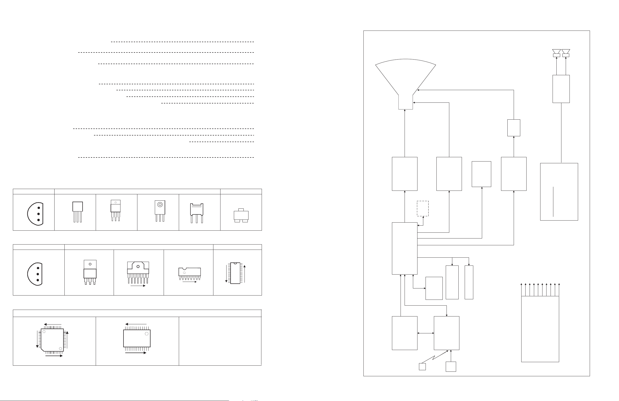
SEMICONDUCTOR SHAPES
BLOCK DIAGRAM
WAVEFORM DIAGRAMS
CIRCUIT DIAGRAMS
PATTERN DIAGRAMS
VOLTAGE TABLES
COPYRIGHT 2002 VICTOR COMPANY OF JAPAN, LTD.
2-1
2-2
2-3
2-4
2-5
2-17
2-21
No.51936
Mar. 2002
Page 2

AV29BF10ENS
STANDARD CIRCUIT DIAGRAM
NOTE ON USING CIRCUIT DIAGRAMS
1.SAFETY
The components identified by the symbol and shading are
critical for safety. For continued safety replace safety critical
components only with manufactures recommended parts.
2.SPECIFIED VOLTAGE AND WAVEFORM VALUES
The voltage and waveform values have been measured under the
foll owing conditions.
(1)Input signal : Colour bar signal
(2)Setting positions of
each knob/button and
variable resistor
(3)Internal resistance of tester
:DC 20k
/V
(4)Oscilloscope sweeping time
:H
20µS/div
:V
5mS/div
:Others
Sweeping time is
specified
(5)Voltage values
:All DC voltage values
Sin ce the voltage val ues of signa l circuit vary to some exten t
according to adjustments, use them as reference values.
3.INDICATIONS ON THE CIRCUIT DIAGRAM
(1)Resistors
Resistance value
No unit :[
]
K
:[K
]
M
Ty pe
No indication
:Carbon resistor
OM R
:Oxi de metal film resistor
MFR
:Met al film resistor
MPR
:Metal plate resistor
UNFR
:Uninflammable resistor
FR
:Fusible resistor
Compositi on resistor 1/2 [W] is spec ified a s 1/2S or Comp.
(2)Capacitors
: Original setting position
when shipped
4.NOTE FOR RE PAIRI NG SERVICE
This model's power circuit is partly different in the GND. The
difference of the GND is shown by the LIVE side GND and the
ISOLATED(NEUTRAL) side GND.Therefore, care must be
taken for the following points.
(1)Do not touch the LIVE side GND or the LIVE side GND and the
ISOLATED(NEUTRAL) side GND simultaneously. If the above
caution is not respected, an electric shock may be caused.
Therefore, make sure that the power cord is surely removed from
the receptacle when, for e xample, the chassis is pulled out.
(2)Do not short between the LIVE side GND and ISOLATED(NEUTRAL)
side GND or never measure with a measuring apparatus measure
with a measuring apparatus ( oscilloscope, etc.) the LIVE side GND
and ISOLATED(NEUTRAL) side GND at t he same time.
If the above precaution is not respected , a fuse or any parts will be broken.
Since the circuit diagram is a standard one, the circuit and
circuit constants may be subject to change for improvement
without any notice.
NOTE
Due improvement in performance, some part numbers show
in th e circui t diag ram may not agree with th ose indicate d in
the part list.
When ordering parts, please use the numbers that appear
in the Parts List.
Ty pe
MM
:Metalized mylar capacitor
PP
:Polypropylene capacitor
MPP
:Metalized polypropylene capacitor
MF
:Metalized film capacitor
TF
:Thin film capacitor
BP
:Bipolar electrolytic capacitor
TAN
:Tantalum capacitor
(3) Coi ls
No unit
:[
µ
H]
Others
:As specified
:[M ]
Capacitance value
1 or higher :[pF]
less than 1
:[µF]
Withstand voltage
No indication :DC5 0[V]
Others :DC withstand voltage [V]
AC indicated
:AC withstand voltage [V]
Electrolytic Capacitors
47/50[Example]:Capac itance value [µF]/withstand voltage[V]
No indication
:Ceramic capacitor
AV29BF10ENS
AV29BF10EPS
AV29BF10EES
AV29BF10EPS
AV29BF10EES
WAVEFORM DIAGRAMS
MAIN PWB
AV29BF10ENS
AV29BF10EPS
AV29BF10EES
Q600 C
1.3Vp-p(H)
IC200 31pin
1.8Vp-p(H)
IC200 40pin
IC200 56pin IC600 5pin
0.7Vp-p(H) 80Vp-p(H)
CRT SOCKET PWB
2-4
IC600 7pin
0.6Vp-p(H) 1400Vp-p(H)
IC900 7pin IC900 8pin IC900 9pin
3.5Vp-p(H)
Q600 B
25Vp-p(H)
IC200 32pin
2Vp-p(H)
IC200 33pin
2Vp-p(H)
IC600 1pin
0.6Vp-p(V)
No.51936
Q602 C
110Vp-p(H)100Vp-p(H)100Vp-p(H)
Mar. 2002 No. 51936
Page 3
AV29BF10ENS
TUNER
PLL
(channel/frequency)
VIDEO PROCESSOR
TDA 8885 H
(BOCMA)
(PHILIPS)
RGB AMPLIFIER
TDA 6108
(PHILIPS)
TV TEXT PRO
SDA 555X
(SIEMENS)
COMB FILTER
TDA 9181
(PHILIPS)
IR
KEY
PAD
VERTICAL AMPLIFIER
STV 9379FA
(ST)
E/W
CORRECTION
HORIZONTAL
OUTPUT
BU 2508
FBT
FRONT AV IN
SCART 1
------------------------------
SCART 2
SMPS
MC 44608
(MOTOROLA)
+
PASSIVE PFC
SOUND PROCESSOR
G/S NICAM STEREO (MSP 3410 G)
MICRONAS
CRT
VIDEO
SWITCH
TEA 6415
(ST)
150V DC
+3.3V
+3.3V (ST-BY)
+8V
+5V
-14V(audio)
+14V(audio)
+2.5V(ST-BY)
+14V
+22V
MAIN AUDIO
AMPLIFIER
TDA 7265 (
ST
)
8 ohm
12W
8 ohm
12W
AV29BF10EPS
AV29BF10EES
CONTENTS
AV29BF10ENS
AV29BF10EPS
AV29BF10EES
BLOCK DIAGRAM
SEMICONDUCTOR SHAPES
BLOCK DIAGRAM
WAVEFORM DIAGRAMS
CIRCUIT DIAGRAMS
MAIN PWB CIRCUIT DIAGRAM
CRT SOCKET PWB CIRCUIT DIAGRAM
FRONT CONTROL PWB CIRCUIT DIAGRAM
FRONT AV + HEADPHONE JACK PWB CIRCUIT DIAGRAM
PATTERN DIAGRAMS
MAIN PWB PATTERN
CRT SOCKET PWB PATTERN
FRONT CONTROL & FRONT AV + HEADPHONE JACK PWB PATTERN
VOLTAGE TABLES
SEMICONDUCTOR SHAPES
TRANSISTOR
BOTTOM V IEW
E
C
B
ECB
BCE
(G)(D)(S )
FRONT VI EW
ECB
ECB
2-2
2-3
2-4
2-5
2-15
2-15
2-16
2-17
2-19
2-20
2-21
TOP VIEW
CHIP TR
C
BE
IC
BOTTOM VIEW FRONT VIEW TOP VIEW
OUT
E
CHIP IC
IN
N
N
N
1
N
IN OUTE
1 N
TOP VIEW
1
N
1 N
1
N
2-2
No.51936No.51936
2-3
Page 4

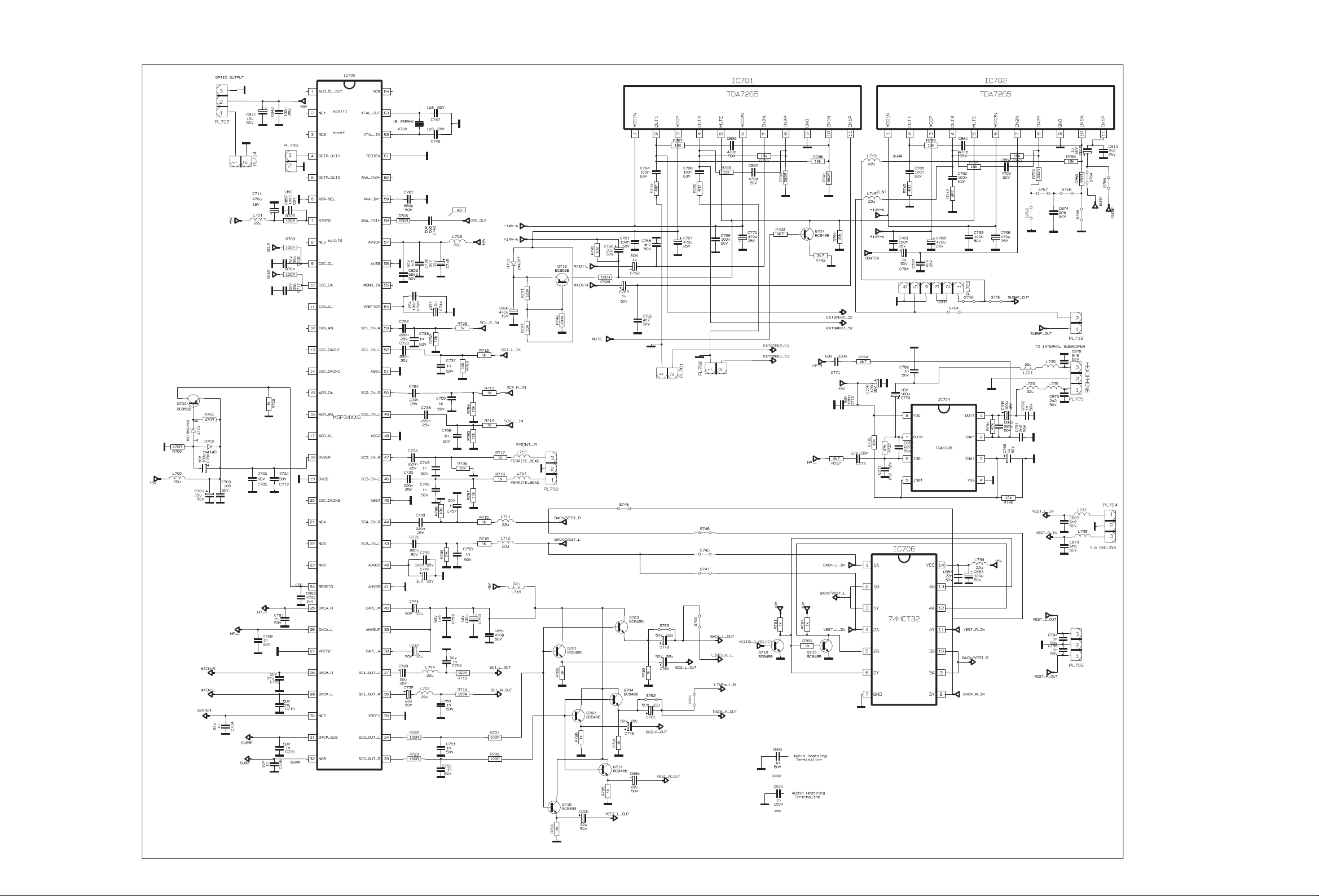
CIRCUIT DIAGRAMS
MAIN PWB CIRCUIT DIAGRAM (1/5)
AV29BF10ENS
A V29BF10EPS
A V29BF10EES
AV29BF10ENS
AV29BF10EPS
AV29BF10EES
MAIN PWB VE-20082209(A V29BF10ENS), VE-20083311(A V29BF10EPS), VE-20082155(A V29BF10EES)
No.51936
2-5 2-6
No.51936
DIFFERENCE LIST
AV29BF10ENS AV29BF10EPS / EES
C368
CAP CER 4.7NF 50V K B
J116
KISA DEVRE TEL. 0.6MM
CAB2
CABLE 1P R2.6(55CM)
C372
CAP SMD 100PF 50V J(0603)
C369
CAP SMD 4.7NF 50V K (0603)
R213
RES SMD 1/16W 10K V (0603)
Z200
FILTER SAW K9356
L223
FERRITE BEAD ACB2012H-300
Z201
FILTER SAW K9358M
J216
KISA DEVRE TEL. 0.6MM
J276
KISA DEVRE TEL. 0.6MM
C610
OPEN
R317
OPEN
D211
OPEN
Q205
OPEN
A-A
OPEN
J111
OPEN
E
OPEN
CAB4
OPEN
CAB5
OPEN
C379
OPEN
C380
OPEN
C381
OPEN
C382
OPEN
C383
OPEN
R419
OPEN
R418
OPEN
R268
OPEN
R416
OPEN
S200
OPEN
S201
OPEN
C-C
OPEN
C241
OPEN
B-B
OPEN
J305
OPEN
J306
OPEN
CAP CER 47NF 50V Z B
OPEN
OPEN
OPEN
CAP SMD 47NF 50V K (0603)
RES SMD 1/16W 22K J (0603)
FILTER SAW K9356M
OPEN
FILTER SAW OFWK3953M
OPEN
OPEN
CAP CER 100PF 50V J CH
RES CF 1/4W 100R J
DIODE 1N4148 SMD
TR BC848B SMD
CABLE BLACK 1P 12CM
KISA DEVRE TEL. 0.6MM
CABLE 1P R2.6 (35CM)
CABLE 0.6MM BLUE 2 CM
CABLE 0.6MM BLUE 2 CM
CAP SMD 220PF 50V J (0603)
CAP SMD 4.7NF 50V K (0603)
CAP SMD 4.7NF 50V K (0603)
CAP SMD 4.7NF 50V K (0603)
CAP SMD 4.7NF 50V K (0603)
RES SMD 1/16W 1KJ (0603)
RES SMD 1/16W 2.2KJ (0603)
RES SMD 1/16W 33KJ (0603)
RES SMD 1/16W 6.8KJ (0603)
JUMPER SMD 0603
JUMPER SMD 0603
CABLE 1P R2.6 (19CM)
CAP SMD 100NF 16V K R (0603)
CABLE 1P R2.6 (16CM)
KISA DEVRE TEL. 0.6MM
KISA DEVRE TEL. 0.6MM
Page 5
MAIN PWB CIRCUIT DIAGRAM (2/5)
AV29BF10ENS
A V29BF10EPS
A V29BF10EES
AV29BF10ENS
A V29BF10EPS
A V29BF10EES
MAIN PWB VE-20082209(A V29BF10ENS), VE-20083311(A V29BF10EPS), VE-20082155(A V29BF10EES)
No.51936 No.51936
2-7 2-8
Page 6

MAIN PWB CIRCUIT DIAGRAM (3/5)
AV29BF10ENS
A V29BF10EPS
A V29BF10EES
AV29BF10ENS
AV29BF10EPS
AV29BF10EES
MAIN PWB VE-20082209(A V29BF10ENS), VE-20083311(A V29BF10EPS), VE-20082155(A V29BF10EES)
No.51936
2-9
2-10
No.51936
Page 7

MAIN PWB CIRCUIT DIAGRAM (4/5)
AV29BF10ENS
A V29BF10EPS
A V29BF10EES
AV29BF10ENS
A V29BF10EPS
A V29BF10EES
MAIN PWB VE-20082209(A V29BF10ENS), VE-20083311(A V29BF10EPS), VE-20082155(A V29BF10EES)
No.51936 No.51936
2-11 2-12
Page 8

MAIN PWB CIRCUIT DIAGRAM (5/5)
AV29BF10ENS
A V29BF10EPS
A V29BF10EES
AV29BF10ENS
AV29BF10EPS
AV29BF10EES
MAIN PWB VE-20082209(A V29BF10ENS), VE-20083311(A V29BF10EPS), VE-20082155(A V29BF10EES)
No.51936
2-13 2-14
No.51936
Page 9

CRT SOCKET PWB CIRCUIT DIA GRAM
AV29BF10ENS
A V29BF10EPS
A V29BF10EES
AV29BF10ENS
A V29BF10EPS
A V29BF10EES
FRONT CONTROL PWB CIRCUIT DIA GRAM
CRT SOCKET PWB VE-20072781
(AV29BF10EES), VE-20062535(AV29BF10ENS, AV29BF10EPS)
FRONT AV + HEADPHONE JACK PWB CIRCUIT DIAGRAM
FRONT AV + HEAD PHONE JACK PWB
VE-20083088
FRONT CONTROL PWB
VE-20083267
No.51936 No.51936
2-15 2-16
Page 10

PATTERN DIAGRAMS MAIN PWB PATTERN (PARTS SIDE)
AV29BF10ENS
A V29BF10EPS
A V29BF10EES
AV29BF10ENS
AV29BF10EPS
AV29BF10EES
No.51936
2-17 2-18
No.51936
Page 11

CRT SOCKET PWB PATTERN (PARTS SIDE)
AV29BF10ENS
A V29BF10EPS
A V29BF10EES
TOP
AV29BF10ENS
A V29BF10EPS
A V29BF10EES
FRONT CONTROL PWB PATTERN
(PARTS SIDE)
TOP
FRONT AV + HEADPHONE JACK
PWB PATTERN (PARTS SIDE)
FRONT
CRT SOCKET PWB PATTERN (SOLDER SIDE)
TOP
No.51936 No.51936
2-19 2-20
Page 12

AV29BF10ENS
AV29BF10EPS
AV29BF10EES
IC600
PIN NO.
1
2
3
4
IC700
PIN NO.
1
2
3
4
5
6
7
8
9
10
11
12
13
14
15
16
17
18
19
20
21
22
23
24
25
26
27
28
29
30
31
32
IC701
PIN NO.
1
2
3
4
5
6
IC704
PIN NO.
1
2
3
4
VOLTAGE
0
0
0
0
VOLTAGE
2.4
0
0
4.9
0
0
4.9
0
4.5
4.5
2.4
2.4
2.4
1.3
1.3
1.3
1.3
4.9
0
1.3
0
0
0
4.8
0
0
0
0
0
0
0
0
VOLTAGE
-15.0
-0.2
14.8
-0.1
2.4
-15.0
VOLTAGE
2.4
2.4
2.4
0
PIN NO.
5
6
7
PIN NO.
33
34
35
36
37
38
39
40
41
42
43
44
45
46
47
48
49
50
51
52
53
54
55
56
57
58
59
60
61
62
63
64
PIN NO.
7
8
9
10
11
PIN NO.
5
6
7
8
VOLTAGE
0.4
15.4
7.5
VOLTAGE
3.6
3.6
0
3.6
3.6
6.8
7.8
6.8
0
3.6
3.6
3.6
0
3.6
3.6
0
3.6
3.6
0
3.6
3.6
2.5
NC
0
4.9
1.4
1.4
NC
0
2.3
2.2
NC
VOLTAGE
0
0
0
0
0
VOLTAGE
2.4
2.4
2.4
4.9
E (D) C (S) B (G)
Q100
Q101
Q102
Q103
Q104
Q105
Q106
Q107
Q200
Q209
Q210
Q211
Q212
Q215
Q216
Q218
Q228
Q229
Q500
Q501
Q502
Q503
Q504
Q505
Q506
Q507
Q508
Q510
Q511
Q512
Q513
Q514
Q515
Q516
Q517
Q600
Q602
Q604
Q605
Q700
Q701
Q701
Q703
Q704
Q707
Q716
237
0
410
0
0
0
147.3
7.8
1.4
1.3
3.6
0.6
2.7
3.4
3.4
0.7
2.2
1.4
4.6
4.6
3.0
3.1
3.2
0
0
0
0
4.2
2.5
2.5
0
0
0
0
0
0
0
0
7.5
4.9
3.0
3.0
3.0
3.0
2.4
14.9
CRT SOCKET PWB
IC900
PIN NO.
1
2
3
4
5
Q100
Q101
VOLTAGE
2.7
2.7
3.6
0
5.6
E(D) C(S) B(G)
237
0
0
14.6
0
1.3
0
0
146.9
8.4
7.7
0
0
7.8
0
0
0
7.8
7.7
7.7
3.0
3.0
4.6
4.6
3.2
2.0
0.1
3.3
2.5
3.0
14.8
-15.0
5.7
7.8
7.5
2.6
3.1
0
-158.5
32.8
0
4.8
7.8
7.8
7.8
7.8
2.4
2.4
PIN NO.
6
7
8
9
0
14.6
1.2
0
1.9
0
0.6
0.6
0
163.8
2.0
0.6
2.9
0.3
0
2.8
2.8
1.3
2.7
2
2.2
2.3
2.2
2.3
2.6
0
0.7
0.5
0.5
7.6
3.2
3.2
0.3
7.5
0
0
0
14.1
-0.1
2.9
7.5
4.1
3.6
3.6
3.6
3.6
3.0
14.9
VOLTAGE
199
116
111.5
111.9
1.2
0
VOLTAGE TABLES
MAIN PWB
IC100
PIN NO.
1
2
3
4
IC102
PIN NO.
1
2
3
IC106
PIN NO.
1
2
3
4
IC107
PIN NO.
1
2
3
4
IC200
PIN NO.
1
2
3
4
5
6
7
8
9
10
11
12
13
14
15
16
17
18
19
20
21
22
23
24
25
26
27
28
29
30
31
32
VOLTAGE
8.4
7.3
4.9
13.7
VOLTAGE
8.3
0
4.9
VOLTAGE
1.0
0
4.9
0
VOLTAGE
2.6
1.4
0.1
0
VOLTAGE
1.8
1.8
2.1
3.6
3.8
0
2.4
1.8
1.8
2.5
3.0
7.2
3.3
2.3
3.0
4.6
4.5
3.8
0
1.2
3.6
2
7.0
3.6
0
2.8
2.8
2.2
3.7
5.4
2.7
2.7
IC101
PIN NO.
IC103
PIN NO.
PIN NO.
PIN NO.
PIN NO.
33
34
35
36
37
38
39
40
41
42
43
44
45
46
47
48
49
50
51
52
53
54
55
56
57
58
59
60
61
62
63
64
AV29BF10ENS
AV29BF10EPS
AV29BF10EES
IC201
VOLTAGE
1
2
3
1
2
3
2.0
3.3
8.4
VOLTAGE
14.6
0
7.8
PIN NO.
1
2
3
4
5
6
7
8
9
10
VOLTAGE
3.1
4.5
2.7
4.5
2.7
3.6
7.5
2.7
7.5
3.6
PIN NO.
11
12
13
14
15
16
17
18
19
20
VOLTAGE
3.0
0
2.7
2.8
2.0
2.0
2.8
2.8
0
2.7
IC203
VOLTAGE
5
6
7
8
5
6
7
8
1.9
13.7
0
188.1
VOLTAGE
1.0
0
1.3
13.6
VOLTAGE
2.6
2.9
3.3
3.7
3.3
0.1
3.3
3.2
0
0
0
0
0
2.5
0
0
3.9
4.9
1.5
1.5
7.8
2.8
3.9
1.6
0.3
2.8
3.8
0
0
2.9
2.4
2.4
PIN NO.
1
2
3
4
5
6
7
8
IC500
PIN NO.
1
2
3
4
5
6
7
8
9
10
11
12
13
14
15
16
17
18
19
20
21
22
23
24
25
26
IC502
PIN NO.
1
2
3
4
IC503
PIN NO.
1
2
3
4
VOLTAGE
1.4
0
1.5
0
1.3
0
2.9
0.6
VOLTAGE
3.2
0
1.9
3.2
3.2
3.2
3.2
0
2.4
0
3.3
0.8
2.4
0
2.4
0
0
1.5
0.6
1.1
3.2
3.2
3.2
3.6
3.0
3.0
VOLTAGE
0
0
0
0
VOLTAGE
3.1
4.2
4.2
-12.1
PIN NO.
9
10
11
12
13
14
15
16
PIN NO.
27
28
29
30
31
32
33
34
35
36
37
38
39
40
41
42
43
44
45
46
47
48
49
50
51
52
PIN NO.
5
6
7
8
PIN NO.
5
6
7
8
VOLTAGE
0
0.7
4.9
4.9
0
1.5
3.2
0.8
VOLTAGE
0
3.2
0
3.2
3.2
3.2
3.2
0.4
0.5
0
2.4
0.3
0.2
0.1
0.2
2.4
0
3.2
0
0
1.0
1.3
3.2
3.2
0
3.2
VOLTAGE
3.0
3.0
3.2
3.2
VOLTAGE
4.2
4.2
3.0
12.0
2-22
No.51936No.51936
2-21
Page 13

AV29BF10ENS
AV29BF10EPS
AV29BF10EES
IC600
PIN NO.
1
2
3
4
IC700
PIN NO.
1
2
3
4
5
6
7
8
9
10
11
12
13
14
15
16
17
18
19
20
21
22
23
24
25
26
27
28
29
30
31
32
IC701
PIN NO.
1
2
3
4
5
6
IC704
PIN NO.
1
2
3
4
VOLTAGE
0
0
0
0
VOLTAGE
2.4
0
0
4.9
0
0
4.9
0
4.5
4.5
2.4
2.4
2.4
1.3
1.3
1.3
1.3
4.9
0
1.3
0
0
0
4.8
0
0
0
0
0
0
0
0
VOLTAGE
-15.0
-0.2
14.8
-0.1
2.4
-15.0
VOLTAGE
2.4
2.4
2.4
0
PIN NO.
5
6
7
PIN NO.
33
34
35
36
37
38
39
40
41
42
43
44
45
46
47
48
49
50
51
52
53
54
55
56
57
58
59
60
61
62
63
64
PIN NO.
7
8
9
10
11
PIN NO.
5
6
7
8
VOLTAGE
0.4
15.4
7.5
VOLTAGE
3.6
3.6
0
3.6
3.6
6.8
7.8
6.8
0
3.6
3.6
3.6
0
3.6
3.6
0
3.6
3.6
0
3.6
3.6
2.5
NC
0
4.9
1.4
1.4
NC
0
2.3
2.2
NC
VOLTAGE
0
0
0
0
0
VOLTAGE
2.4
2.4
2.4
4.9
E (D) C (S) B (G)
Q100
Q101
Q102
Q103
Q104
Q105
Q106
Q107
Q200
Q209
Q210
Q211
Q212
Q215
Q216
Q218
Q228
Q229
Q500
Q501
Q502
Q503
Q504
Q505
Q506
Q507
Q508
Q510
Q511
Q512
Q513
Q514
Q515
Q516
Q517
Q600
Q602
Q604
Q605
Q700
Q701
Q701
Q703
Q704
Q707
Q716
237
0
410
0
0
0
147.3
7.8
1.4
1.3
3.6
0.6
2.7
3.4
3.4
0.7
2.2
1.4
4.6
4.6
3.0
3.1
3.2
0
0
0
0
4.2
2.5
2.5
0
0
0
0
0
0
0
0
7.5
4.9
3.0
3.0
3.0
3.0
2.4
14.9
CRT SOCKET PWB
IC900
PIN NO.
1
2
3
4
5
Q100
Q101
VOLTAGE
2.7
2.7
3.6
0
5.6
E(D) C(S) B(G)
237
0
0
14.6
0
1.3
0
0
146.9
8.4
7.7
0
0
7.8
0
0
0
7.8
7.7
7.7
3.0
3.0
4.6
4.6
3.2
2.0
0.1
3.3
2.5
3.0
14.8
-15.0
5.7
7.8
7.5
2.6
3.1
0
-158.5
32.8
0
4.8
7.8
7.8
7.8
7.8
2.4
2.4
PIN NO.
6
7
8
9
0
14.6
1.2
0
1.9
0
0.6
0.6
0
163.8
2.0
0.6
2.9
0.3
0
2.8
2.8
1.3
2.7
2
2.2
2.3
2.2
2.3
2.6
0
0.7
0.5
0.5
7.6
3.2
3.2
0.3
7.5
0
0
0
14.1
-0.1
2.9
7.5
4.1
3.6
3.6
3.6
3.6
3.0
14.9
VOLTAGE
199
116
111.5
111.9
1.2
0
MAIN PWB
IC100
PIN NO.
1
2
3
4
IC102
PIN NO.
1
2
3
IC106
PIN NO.
1
2
3
4
IC107
PIN NO.
1
2
3
4
IC200
PIN NO.
1
2
3
4
5
6
7
8
9
10
11
12
13
14
15
16
17
18
19
20
21
22
23
24
25
26
27
28
29
30
31
32
VOLTAGE
8.4
7.3
4.9
13.7
VOLTAGE
8.3
0
4.9
VOLTAGE
1.0
0
4.9
0
VOLTAGE
2.6
1.4
0.1
0
VOLTAGE
1.8
1.8
2.1
3.6
3.8
0
2.4
1.8
1.8
2.5
3.0
7.2
3.3
2.3
3.0
4.6
4.5
3.8
0
1.2
3.6
2
7.0
3.6
0
2.8
2.8
2.2
3.7
5.4
2.7
2.7
IC101
PIN NO.
IC103
PIN NO.
PIN NO.
PIN NO.
PIN NO.
33
34
35
36
37
38
39
40
41
42
43
44
45
46
47
48
49
50
51
52
53
54
55
56
57
58
59
60
61
62
63
64
AV29BF10ENS
AV29BF10EPS
AV29BF10EES
IC201
VOLTAGE
1
2
3
1
2
3
2.0
3.3
8.4
VOLTAGE
14.6
0
7.8
PIN NO.
1
2
3
4
5
6
7
8
9
10
VOLTAGE
3.1
4.5
2.7
4.5
2.7
3.6
7.5
2.7
7.5
3.6
PIN NO.
11
12
13
14
15
16
17
18
19
20
VOLTAGE
3.0
0
2.7
2.8
2.0
2.0
2.8
2.8
0
2.7
IC203
VOLTAGE
5
6
7
8
5
6
7
8
1.9
13.7
0
188.1
VOLTAGE
1.0
0
1.3
13.6
VOLTAGE
2.6
2.9
3.3
3.7
3.3
0.1
3.3
3.2
0
0
0
0
0
2.5
0
0
3.9
4.9
1.5
1.5
7.8
2.8
3.9
1.6
0.3
2.8
3.8
0
0
2.9
2.4
2.4
PIN NO.
1
2
3
4
5
6
7
8
IC500
PIN NO.
1
2
3
4
5
6
7
8
9
10
11
12
13
14
15
16
17
18
19
20
21
22
23
24
25
26
IC502
PIN NO.
1
2
3
4
IC503
PIN NO.
1
2
3
4
VOLTAGE
1.4
0
1.5
0
1.3
0
2.9
0.6
VOLTAGE
3.2
0
1.9
3.2
3.2
3.2
3.2
0
2.4
0
3.3
0.8
2.4
0
2.4
0
0
1.5
0.6
1.1
3.2
3.2
3.2
3.6
3.0
3.0
VOLTAGE
0
0
0
0
VOLTAGE
3.1
4.2
4.2
-12.1
PIN NO.
9
10
11
12
13
14
15
16
PIN NO.
27
28
29
30
31
32
33
34
35
36
37
38
39
40
41
42
43
44
45
46
47
48
49
50
51
52
PIN NO.
5
6
7
8
PIN NO.
5
6
7
8
VOLTAGE
0
0.7
4.9
4.9
0
1.5
3.2
0.8
VOLTAGE
0
3.2
0
3.2
3.2
3.2
3.2
0.4
0.5
0
2.4
0.3
0.2
0.1
0.2
2.4
0
3.2
0
0
1.0
1.3
3.2
3.2
0
3.2
VOLTAGE
3.0
3.0
3.2
3.2
VOLTAGE
4.2
4.2
3.0
12.0
No.51936No.51936
2-212-22
Page 14

AV29BF10ENS
AV29BF10EPS
AV29BF10EES
VICTOR COMPANY OF JAPAN, LIMITED
HOME AV NETWORK BUSINESS UNIT. 12, 3-chome, Moriya-cho, Kanagawa-ku, Yokohama, Kanagawa-prefecture, 221-8528, Japan
Printed in Japan
VP 0203
DP8080
 Loading...