

Page 1
SERVICE MANUAL
COLOR TELEVISION
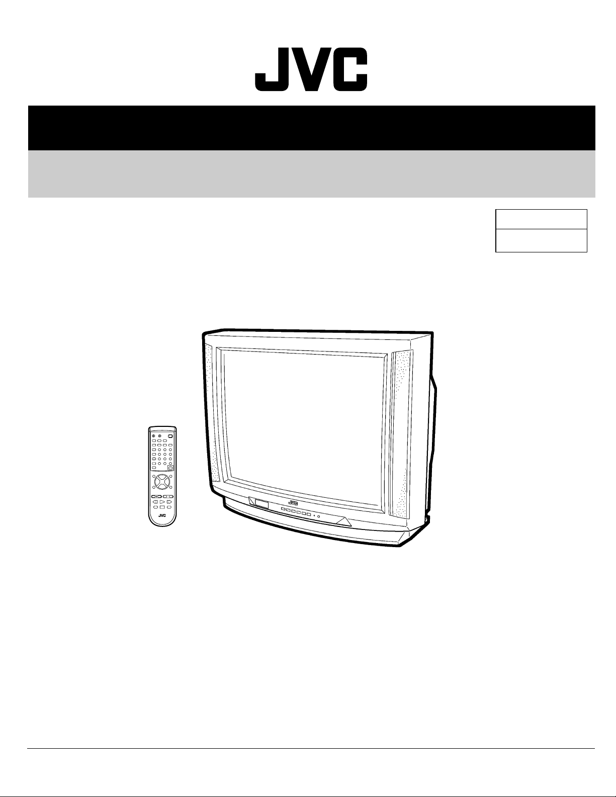
AV-27D502
BASIC CHASSIS
AC
AV-27D502
AV-27D502
TV
/R
/S
CONTENTS
a SPECIFICATIONS ....................................................................................................................................2
a SAFETY PRECAUTIONS ........................................................................................................................3
a FEATURES ..............................................................................................................................................5
a MAIN DIFFERENCE LIST........................................................................................................................6
a HOW TO IDENTIFY MODELS ..................................................................................................................6
a FUNCTIONS .............................................................................................................................................7
a SPECIFIC SERVICE INSTRUCTIONS ....................................................................................................8
a SERVICE ADJUSTMENTS ....................................................................................................................12
¤ STANDARD CIRCUIT DIAGRAM (APPENDIX) .................................................................................. 2-1
a PARTS LIST ...........................................................................................................................................31
COPYRIGHT © 2001 VICTOR COMPANY OF JAPAN, LTD.
No. 51797
Mar. 2001
Page 2

AV-27D502
SPECIFICATIONS
Items Contents
Dimensions (W × H × D)
················································································································································································································
Mass
················································································································································································································
TV RF System
················································································································································································································
Color Sound System
················································································································································································································
TV Receiving Channels and Frequency
VL Band
VH Band
UHF Band
················································································································································································································
CATV Receiving Channels and Frequency
Low Band
High Band
Mid Band
Super Band
Hyper Band
Ultra Band
Sub Mid Band
TV/CATV Total Channel
················································································································································································································
Intermediate Frequency
Video IF Carrier
Sound IF Carrier
Color Sub Carrier
················································································································································································································
Power Input
Power Consumption
················································································································································································································
Picture Tube
High Voltage
················································································································································································································
Speaker
Audio Power Output
················································································································································································································
Video / Audio Input (1 / 2 / 3)
29-5/8” × 23-1/4” × 19-1/2” / 75.2cm × 59.1cm × 49.4cm
71.3 Ibs/32.4kg
CCIR(M)
NTSC, BTSC System (Multi Channel Sound)
(02~06) 54MHz~88MHz
~13) 174MHz~216MHz
(07
(14
~69) 470MHz~806MHz
(02~06, A-8) by (02~06&01)
(07~13) by (07~13)
(A~1) by (14~22)
(J~W) by (23~36) (54MHz~804MHz)
(W+1~W+28) by (37~64)
(W+29~W+84) by (65~125)
(A8, A4~A1) by (01, 96~99)
180 Channels
45.75MHz
41.25MHz (4.5MHz)
3.58MHz
120V AC, 60Hz
123W
27” (68cm) Measured Diagonally
29kV±1.3kV (at zero beam current)
2” × 4-3/4” / 5 × 12cm Oval type × 2
5W × 2
Video(1,3) : 1Vp-p, 75Ø (RCA pin jack)
Audio(1,2,3) : 500mVrms ( -4dBs ), High Impedance (RCA pin jack)
S-Video ( Input 1 / 2 Over )
Y : 1Vp-p Positive (negative sync provided, when terminated with 75Ø)
C : 0.286Vp-p (burst signal, when terminated with 75Ø)
Component Input ( Input 2 )
Y : 1Vp-p positive (negative sync provided, when terminated with 75Ø)
PB/PR : 0.7Vp-p 75 Ø
—
—
················································································································································································································
Audio Output
(Variable)
················································································································································································································
AV Compu link EX Input
················································································································································································································
Antenna terminal
················································································································································································································
Remote Control Unit
Variable : More then 0~1550mVrms (+6dBs)
Low impedance (400Hz when modulated 100%)
3.5mm mini jack
75Ø(VHF/UHF) Terminal, F-Type Connector
RM-C301G-2A
(AA/R6/UM-3 battery × 2)
(RCA pin jack)
Design & specifications are subject to change without notice.
2 No. 51797
Page 3
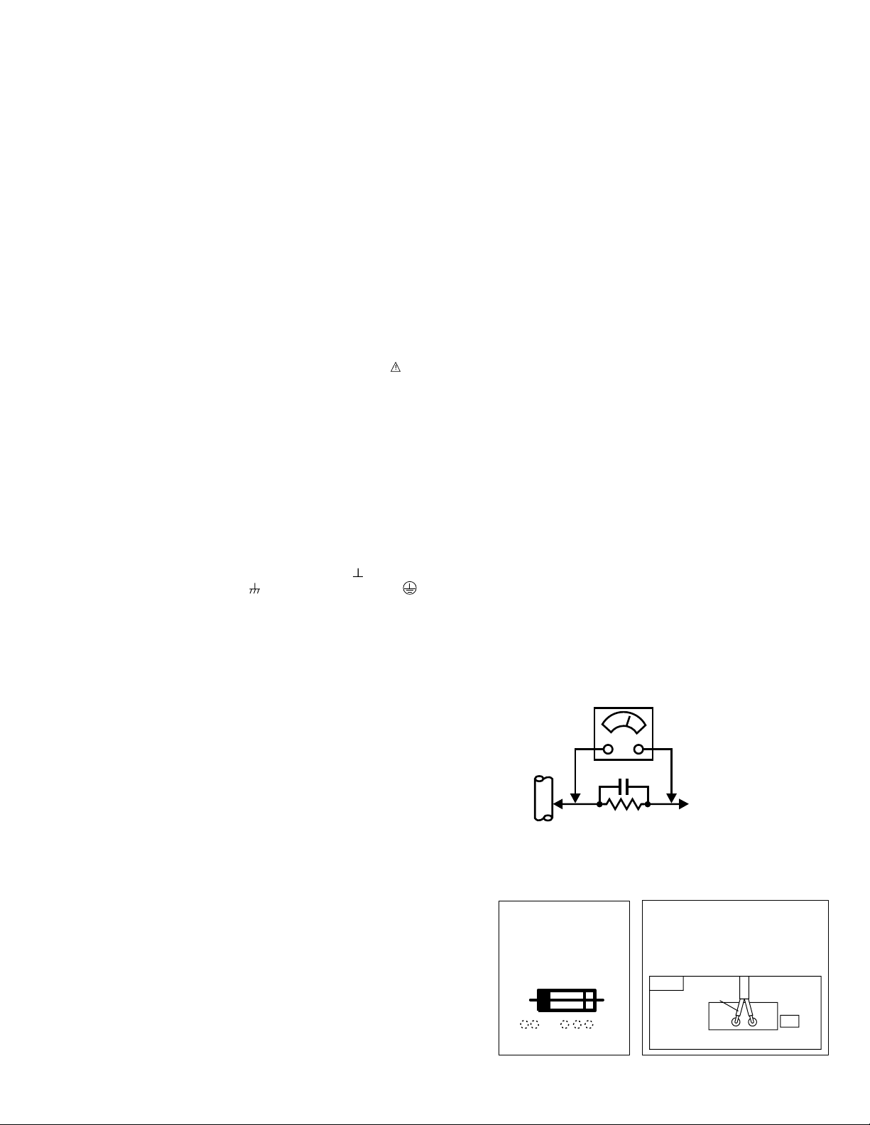
GOOD
EARTH
GROUND
0.15 µF AC-TYPE
AC VOLTMETER
(HAVING 1000Ø/V,
OR MORE SENSITIVITY)
PLACE THIS PROBE
ON EACH EXPOSED
METAL PART
1500Ø 10W
A V
This mark shows a fast
POWER CORD
REPLACEMENT WARNING
Connecting thr white line side of
power cord to “WHT” character side.
operating fuse, the
letters indicated below
show the rating.
PWB
WHT
PW
White line side
SAFETY PRECAUTIONS
1. The design of this product contains special hardware, many circuits
and components specially for safety purposes. For continued protection, no changes should be made to the original design unless
authorized in writing by the manufacturer. Replacement parts must
be identical to those used in the original circuits. Service should be
performed by qualified personnel only.
2. Alterations of the design or circuitry of the products should not be
made. Any design alterations or additions will void the manufacturer's warranty and will further relieve the manufacturer of responsibility for personal injury or property damage resulting therefrom.
3. Many electrical and mechanical parts in the products have special
safety-related characteristics. These characteristics are often not
evident from visual inspection nor can the protection afforded by
them necessarily be obtained by using replacement components
rated for higher voltage, wattage, etc. Replacement parts which have
these special safety characteristics are identified in the parts list of
Service manual. Electrical components having such features are
identified by shading on the schematics and by ( ) on the
parts list in Service manual. The use of a substitute replacement
which does not have the same safety characteristics as the recommended replacement part shown in the parts list of Service manual
may cause shock, fire, or other hazards.
4. Use isolation transformer when hot chassis.
The chassis and any sub-chassis contained in some products are
connected to one side of the AC power line. An isolation transformer
of adequate capacity should be inserted between the product and
the AC power supply point while performing any service on some
products when the HOT chassis is exposed.
5. Don't short between the LIVE side ground and ISOLATED (NEU-
TRAL) side ground or EARTH side ground when repairing.
Some model's power circuit is partly different in the GND. The difference of the GND is shown by the LIVE : ( ) side GND, the
ISOLATED(NEUTRAL) : ( ) side GND and EARTH : ( ) side
GND. Don't short between the LIVE side GND and
ISOLATED(NEUTRAL) side GND or EARTH side GND and never
measure with a measuring apparatus (oscilloscope etc.) the LIVE
side GND and ISOLATED(NEUTRAL) side GND or EARTH side
GND at the same time.
If above note will not be kept, a fuse or any parts will be broken.
6. If any repair has been made to the chassis, it is recommended that
the B1 setting should be checked or adjusted (See ADJUSTMENT
OF B1 POWER SUPPLY).
7. The high voltage applied to the picture tube must conform with that
specified in Service manual. Excessive high voltage can cause an
increase in X-Ray emission, arcing and possible component damage, therefore operation under excessive high voltage conditions
should be kept to a minimum, or should be prevented. If severe
arcing occurs, remove the AC power immediately and determine
the cause by visual inspection (incorrect installation, cracked or
melted high voltage harness, poor soldering, etc.). To maintain the
proper minimum level of soft X-Ray emission, components in the
high voltage circuitry including the picture tube must be the exact
replacements or alternatives approved by the manufacturer of the
complete product.
8. Do not check high voltage by drawing an arc. Use a high voltage
meter or a high voltage probe with a VTVM. Discharge the picture
tube before attempting meter connection, by connecting a clip lead
to the ground frame and connecting the other end of the lead through
a 10kØ 2W resistor to the anode button.
9. When service is required, observe the original lead dress. Extra
precaution should be given to assure correct lead dress in the high
voltage circuit area. Where a short circuit has occurred, those components that indicate evidence of overheating should be replaced.
Always use the manufacturer's replacement components.
No. 51797 3
AV-27D502
10. Isolation Check
(Safety for Electrical Shock Hazard)
After re-assembling the product, always perform an isolation check
on the exposed metal parts of the cabinet (antenna terminals, video/
audio input and output terminals, Control knobs, metal cabinet,
screwheads, earphone jack, control shafts, etc.) to be sure the product is safe to operate without danger of electrical shock.
(1) Dielectric Strength Test
The isolation between the AC primary circuit and all metal parts
exposed to the user, particularly any exposed metal part having a
return path to the chassis should withstand a voltage of 1100V AC
(r.m.s.) for a period of one second.
(. . . . Withstand a voltage of 1100V AC (r.m.s.) to an appliance rated
up to 120V, and 3000V AC (r.m.s.) to an appliance rated 200V or
more, for a period of one second.)
This method of test requires a test equipment not generally found in
the service trade.
(2) Leakage Current Check
Plug the AC line cord directly into the AC outlet (do not use a line
isolation transformer during this check.). Using a “Leakage Current
Tester”, measure the leakage current from each exposed metal part
of the cabinet, particularly any exposed metal part having a return
path to the chassis, to a known good earth ground (water pipe, etc.).
Any leakage current must not exceed 0.5mA AC (r.m.s.).
However, in tropical area, this must not exceed 0.2mA AC (r.m.s.).
Alternate Check Method
•
Plug the AC line cord directly into the AC outlet (do not use a line
isolation transformer during this check.). Use an AC voltmeter having 1000 ohms per volt or more sensitivity in the following manner.
Connect a 1500Ø 10W resistor paralleled by a 0.15µF AC-type capacitor between an exposed metal part and a known good earth
ground (water pipe, etc.). Measure the AC voltage across the resistor with the AC voltmeter. Move the resistor connection to each exposed metal part, particularly any exposed metal part having a return path to the chassis, and measure the AC voltage across the
resistor. Now, reverse the plug in the AC outlet and repeat each
measurement. Any voltage measured must not exceed 0.75V AC
(r.m.s.). This corresponds to 0.5mA AC (r.m.s.).
However, in tropical area, this must not exceed 0.3V AC (r.m.s.).
This corresponds to 0.2mA AC (r.m.s.).
11. High voltage hold down circuit check.
After repair of the high voltage hold down circuit, this circuit shall be
checked to operate correctly.
See item “How to check the high voltage hold down circuit”.
Page 4
AV-27D502
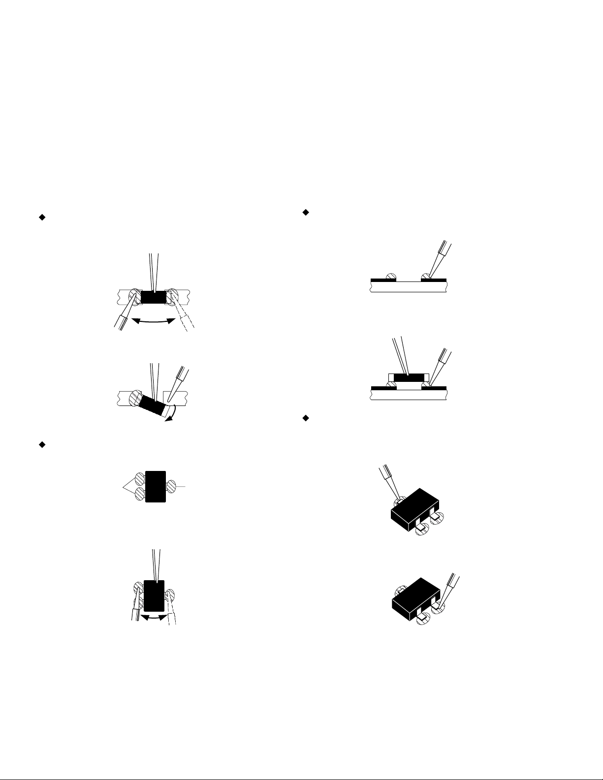
REPLACEMENT OF CHIP COMPONENT
CAUTIONS
a
1. Avoid heating for more than 3 seconds.
2. Do not rub the electrodes and the resist parts of the pattern.
3. When removing a chip part, melt the solder adequately.
4. Do not reuse a chip part after removing it.
SOLDERING IRON
a
1. Use a high insulation soldering iron with a thin pointed end of it.
2. A 30w soldering iron is recommended for easily removing parts.
REPLACEMENT STEPS
a
1. How to remove Chip parts
Resistors, capacitors, etc.
(1) As shown in the figure, push the part with tweezers and alter-
nately melt the solder at each end.
2. How to install Chip parts
Resistors, capacitors, etc.
(1) Apply solder to the pattern as indicated in the figure.
(2) Shift with tweezers and remove the chip part.
Transistors, diodes, variable resistors, etc.
(1) Apply extra solder to each lead.
SOLDER
(2) As shown in the figure, push the part with tweezers and alter-
nately melt the solder at each lead. Shift and remove the chip
part.
SOLDER
(2) Grasp the chip part with tweezers and place it on the solder.
Then heat and melt the solder at both ends of the chip part.
Transistors, diodes, variable resistors, etc.
(1) Apply solder to the pattern as indicated in the figure.
(2) Grasp the chip part with tweezers and place it on the solder.
(3) First solder lead A as indicated in the figure.
A
B
C
(4) Then solder leads B and C.
A
Note : After removing the part, remove remaining solder from the
pattern.
4 No. 51797
B
C
Page 5
FEATURES
IC702
E2PROM 4k bit
IC701
MAIN MICON
IF2
SCL 1 SDA 1
SCL 0 SDA 0
AFC 2
AFC 1
Remote
control
unit
IC301
PIP
CONTROL
IC001
MTS, TONE
SURROUND CONTROL
TU001
TUNER 1
TU001
TUNER 2
IC101
1 CHIP
CONTROL
IC501
AVSW
CONTROL
Full-square CRT (cathode ray tube) reproduces fine textured pic-
•
ture in every detail.
I2C bus control utilizes single chip ICs.
•
Built in Twin Tuner system.
•
Built-in HYPER-SURROUND system.
•
Built-in BBE.
•
Adoption of the Picture-In-Picture (PIP) function.
•
3 LINE DIGITAL COMB FILTER circuit improved picture quality.
•
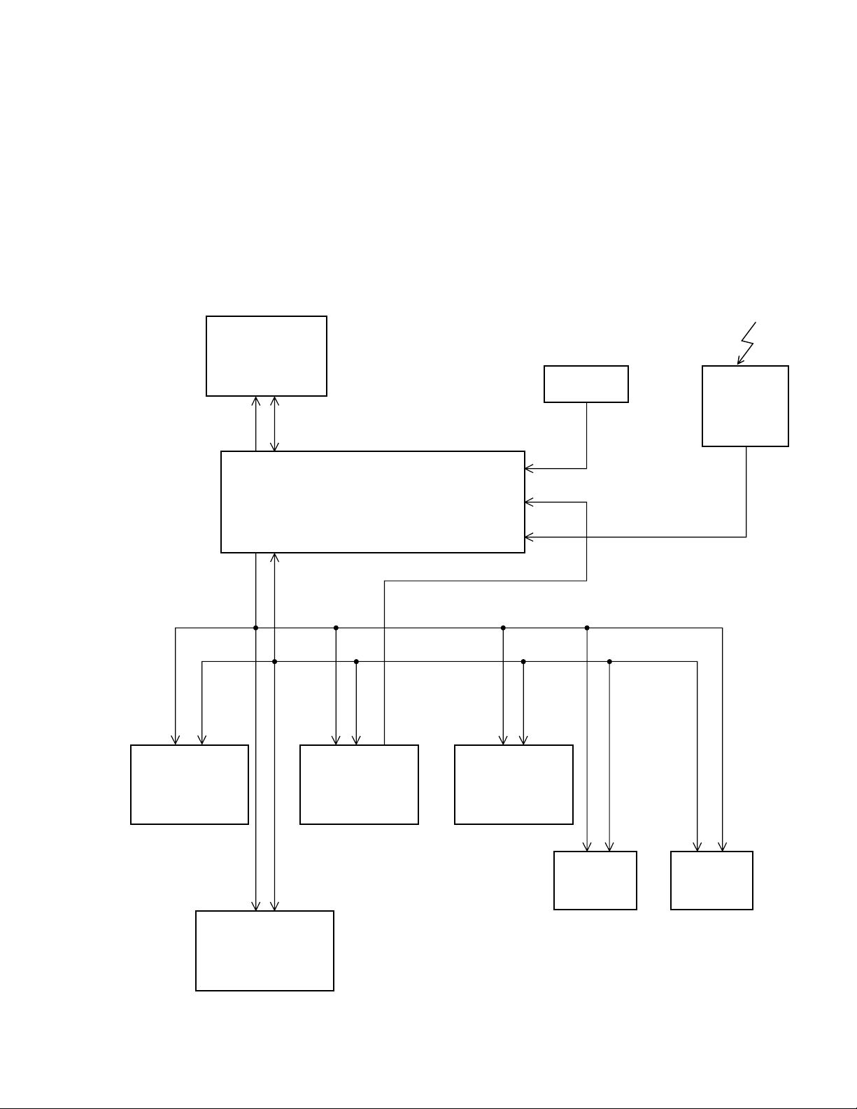
a SYSTEM BLOCK DIAGRAM
AV-27D502
Component input terminal for talking best advantage of Component
•
Video Signal.
Audio Video input terminal. (S-input ×2, V-input ×2)
•
Variable audio output terminal.
•
Closed-caption broadcasts can be viewed.
•
With AV COMPU LINK EX terminal.
•
No. 51797 5
Page 6
AV-27D502
MAIN DIFFERENCE LIST
!
Part name
MAIN PWB SAC-1507A-M2 SAC-1506A-M2
CRT SOCKET PWB SAC-3507A-M2 SAC-3506A-M2
! PICTURE TUBE A68ADT25X01 A68QDN891X001
Model
AV-27D502/R AV-27D502/S
HOW TO IDENTIFY MODELS
The difference between AV-27D502/R and AV-27D502/S is in the PICTURE TUBE.
As the result of the difference in PICTURE TUBE, the MAIN PWB also differ.
!
Part name
! RATING LABEL LC31139-001A-A
------------------------------------------------------------------------------------------------
Model
AV-27D502/R AV-27D502/S
INDICATED AV-27D502
INDICATED AV-27D502
INDICATED “R”
INDICATED “S”
6 No. 51797
Page 7
FUNCTIONS
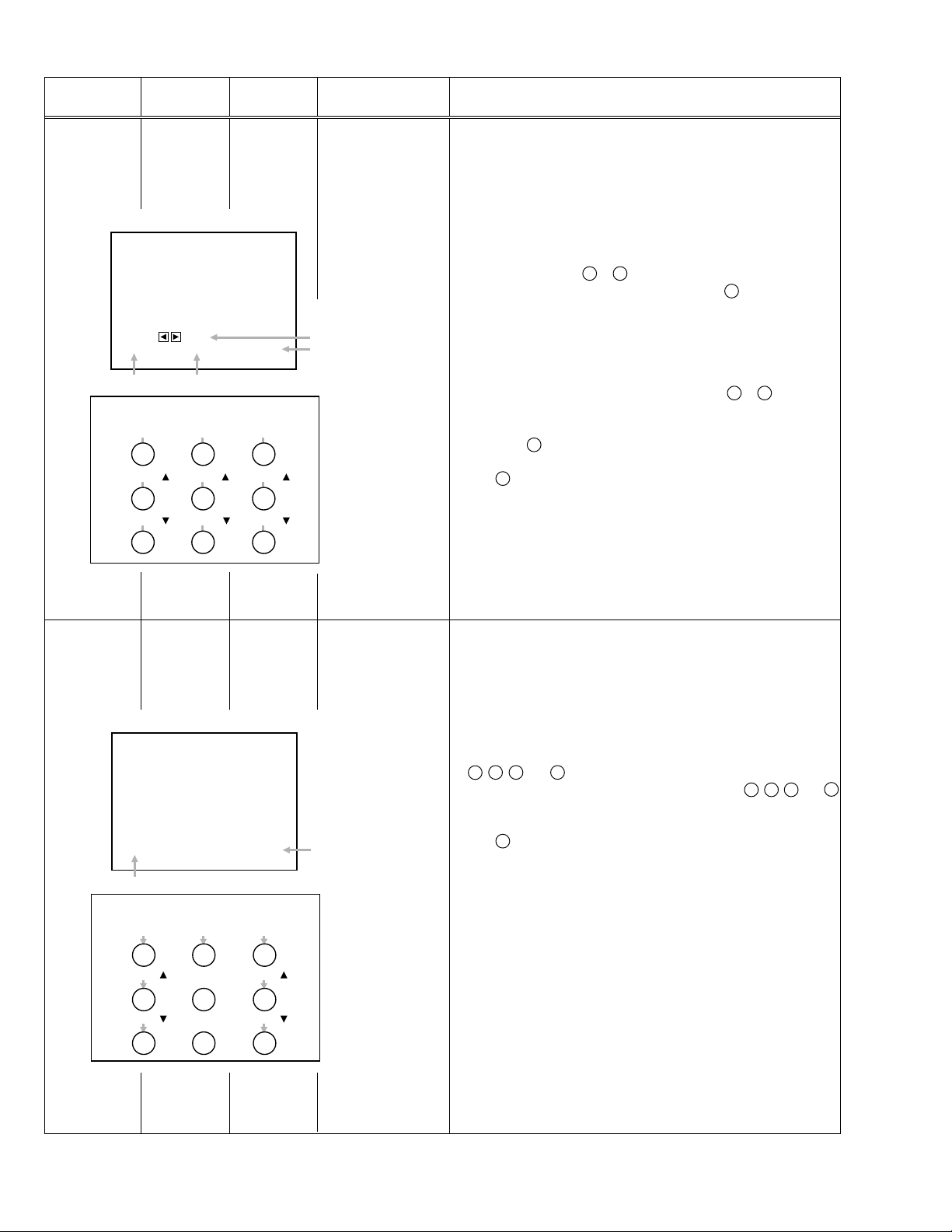
a FRONT PANEL
MENU
CHANNEL
OPERATE
VOLUME
POWER
AV-27D502
ON TIMER
MENU
CHANNEL
VOLUME
a FRONT PANEL DOOR OPENED
INPUT3
VIDEO
L/MONO-AUDIO-R
INPUT3 VIDEO/AUDIO TERMINAL
a REAR PANEL
POWER
a REMOTE CONTROL UNIT
(RM-C301G-2A)
CATV
VCR
CHANNEL
FREEZE
BBE
VOL
VCR CHANNEL
PREV NEXT
DVD
POWER
PIP
ON/MOVE
SWAP
INPUT
100+
1
4
7
CH
CH
+
VCR/DVD
POWER
2
5
8
0
VOL
+
3
6
9
RETURN+
LIGHT
V CHIP
EXIT
PIP OFF
TV/VCR
TV
SOURCE
VIDEO STATUS
DISPLAY
SLEEP TIMER
HYPER SURROUND
RM-C301G
MUTING
MENU
PLAY FFREW
REC STOP
OPEN/CLOSE STILL/PAUSE
PAUSE
TV
No. 51797 7
Page 8

AV-27D502
SPECIFIC SERVICE INSTRUCTIONS
DISASSEMBLY PROCEDURE
REMOVING THE REAR COVER
1. Unplug the power supply cord.
2. Remove the 12 screws marked A as shown in Fig.1.
3. Withdraw the REAR COVER toward you.
[CAUTION]
When reinstalling the rear cover, carefully push it inward after in-
•
serting the MAIN PWB into the rear cover groove.
REMOVING THE CHASSIS
After removing the rear cover.
•
1. Slightly raise the both sides of the chassis by hand and remove the
3 claws marked B under the chassis from the front cabinet as
shown in Fig.1.
2. Withdraw the chassis backward along the rail in the arrow direction
marked C as shown in Fig.1.
(If necessary, take off the wire clamp, connector’s etc.)
When conducting a check with power supplied, be sure to confirm
*
that the CRT earth wire is connected to the CRT SOCKET PWB
and the MAIN PWB.
REMOVING THE TERMINAL BOARD
After removing the rear cover.
•
1. Remove the 4 screws marked D as shown in Fig.1.
2. When you pull out the TERMINAL BOARD in the direction of arrow
marked E as shown in Fig.1, it can be removed.
REMOVING THE SPEAKER
After removing the rear cover.
•
1. Remove the 4 screws marked K as shown in Fig.1.
2. Withdraw the speaker backward.
3. Follow the same steps when removing the other hand speaker.
CHECKING THE MAIN PW BOARD
1. To check the back side of the MAIN PW Board.
1) Pull out the chassis. (Refer to REMOVING THE CHASSIS).
2) Erect the chassis vertically so that you can easily check the back
side of the MAIN PW Board.
[CAUTION]
When erecting the chassis, be careful so that there will be no con-
•
tacting with other PW Board.
Before turning on power, make sure that the CRT earth wire and
•
other connectors are properly connected.
WIRE CLAMPING AND CABLE TYING
1. Be sure clamp the wire.
2. Never remove the cable tie used for tying the wires together.
Should it be inadvertently removed, be sure to tie the wires with a
new cable tie.
REMOVING THE FRONT CONTROL AND FRONT AV
INPUT PW BOARDS
After removing the rear cover and chassis.
•
1. Remove the 3 screws marked F and the 2 screws marked J as
shown in Fig.1.
2. Then remove the FRONT CONTROL PWB and FRONT AV INPUT
PWB.
(If necessary, take off the wire, connector’s etc.)
REMOVING THE LF PW BOARD
After removing the rear cover and chassis.
•
1. Lift the left side of the LF PWB while pressing the 2 PWB stoppers
marked G in the arrow direction marked H as shown in Fig.1.
2. Then remove the LF PWB.
(If necessary, take off the wire, connector’s etc.)
8 No. 51797
Page 9
FRONT CABINET
PICTURE TUBE
SPEAKER
K
(x4)
CRT SOCKET PWB
FRONT AV INPUT PWB
AV-27D502
SPEAKER
REAR COVER
(x2)
J
CLAW
(x3)
F
CLAW
B
K
(x4)
FRONT CONTROL
PWB
PWB
STOPPER
G
H
LF PWB
PWB
G
STOPPER
AV SELECTOR PWB
B
C
PIP PWB
CHASSIS BASE
MAIN PWB
E
D
(x4)
A
(x12)
Fig.1
No. 51797 9
Page 10

AV-27D502
MEMORY IC REPLACEMENT
1. Memory IC
This model use a memory IC.
This memory IC stores data for proper operation of the video and deflection circuits.
When replacing, be sure to use an IC containing this (initial value) data.
2. Memory IC replacement procedure
Procedure Screen display
(1) Power off
Switch off the power and disconnect the power cord from the outlet.
(2) Replace the memory IC
Initial value must be entered into the new IC.
(3) Power on
Connect the power cord to the outlet and switch on the power.
(4) System constant check and setting
1) Press SLEEP TIMER key and, while the indication of “SLEEP TIMER
0 MIN.” is being displayed, press DISPLAY key and VIDEO STATUS
key on the remote control unit simultaneously.
2) The SERVICE MENU screen of Fig.1 is displayed.
3) While the SERVICE MENU is displayed, again simultaneously press
the DISPLAY and VIDEO STATUS keys to display the Fig.2 SYSTEM
CONSTANT screen.
4) Refer to the SYSTEM CONSTANT table and check the setting items.
Where these differ, select the setting item with the MENU UP/DOWN
key and adjust the setting with the MENU LEFT/RIGHT keys. (The
letters of the selected item are displayed in yellow.)
5) After adjusting, release the MENU LEFT/RIGHT key to store the
setting value.
6) Press the EXIT key twice to return the normal screen.
(5) Receive channel setting
Refer to the OPERATING INSTRUCTIONS(USER'S GUIDE) and set the
receive channels (Channels Preset) as described.
(6) User settings
Check the user setting items according to Table 2.
Where these do not agree, refer to the OPERATING INSTRUCTIONS (USER'S GUIDE) and set the items as described.
SERVICE MENU
PICTURE SOUND
THEATER OTHERS
PIP
LOW LIGHT HIGH LIGHT
RF AFC1 RF AFC2
VCO(CW) I2C BUS CTRL
SELECT BY
OPERATE BY
Fig.1
SYSTEM CONSTANT
MODEL :99–
PURITY : NO
CCD : YES
V-CHIP : YES
CAN V-CHIP : YES
EXIT BY
99999
999999999 999
SELECT BY
OPERATE BY
Fig.2
EXIT BY
EX
IT
EX
IT
(7) SERVICE MENU setting
Verify what to set in the SERVICE MENU, and set whatever is
necessary.(Fig.1) Refer to the SERVICE ADJUSTMENT for setting.
10 No. 51797
Page 11
AV-27D502
TABLE 1 (System Constant setting)
Setting item Setting content Setting value
AV-27F802 AV-32F802 AV-36F802 AV-27F702 AV-32F702
MODEL AV-27D502
AV-36D502 AV-32D502 AV-27D502 AV-36F702
AV-32D302 AV-36D302 AV-32D202 AV-36D202
AV-36230 AV-32230 AV-36260 AV-32260 AV-27260
PURITY
CCD
V-CHIP
CAN V-CHIP
YES NO
YES NO
YES NO
YES NO
TABLE 2 (User setting value)
Setting item Setting value
1. Use remote controller keys
POWER OFF
CHANNEL CH-02
VOLUME 5
INPUT TV
HYPER SURROUND OFF
BBE ON
DISPLAY OFF
SLEEP TIMER 0
VIDEO STATUS CHOICE
PIP SOURCE CH-04
PIP ON (PIP POSITION) LEFT LOWR SIDE
2. Setting of MENU
NO
YES
YES
YES
PICTURE ADJUST
TINT CENTER
COLOR CENTER
PICTURE CENTER
BRIGHT CENTER
DETAIL CENTER
NOISE MUTING ON
SET VIDEO STATUS ALL CENTER
SOUND ADJUST
BASS CENTER
TREBLE CENTER
BALANCE CENTER
MTS STEREO
CLOCK/TIMERS
SET CLOCK Unnecessary to set
ON/OFF TIMER NO
INITIAL SETUP
TV SPEAKER ON
COMPONENT-IN NO
LANGUAGE ENG
CLOSED CAPTION OFF
AUTO TUNER SETUP TUNER MODE: AIR
CHANNEL SUMMARY Unnecessary to set
V-CHIP OFF
SET LOCK CODE Unnecessary to set
No. 51797 11
Page 12

AV-27D502
SERVICE ADJUSTMENTS
ADJUSTMENT PREPARATION:
1. You can make the necessary adjustments for this unit with either the remote control unit or with the adjustment equipment and parts
as given below.
2. Adjustment with the remote control unit is made on the basis of the initial setting values, however, the new setting values which set the
screen to its optimum condition may differ from the initial settings.
3. Make sure that AC power is turned on correctly.
4. Turn on the power for the set and test equipment before use, and start the adjustment procedures after waiting at least 30 minutes.
5. Unless otherwise specified, prepare the most suitable reception or input signal for adjustment.
6. Never touch any adjustment parts, which are not specified in the list for this adjustment-variable resistors, transformers, capacitors, etc.
7. Presetting before adjustment.
Unless otherwise specified in the adjustment instructions, preset the following functions with the remote control unit.
User mode setting position
•
VIDEO STATUS STANDARD
HYPER SURROUND OFF
BASS, TREBLE, BALANCE CENTER
TINT, COLOR, PICTURE,
BRIGHT, DETAIL
CENTER
MEASURING INSTRUMENT
1. DC voltmeter(or digital voltmeter)
2. Oscilloscope
3. Signal generator ( Pattern generator ) [NTSC]
4. Remote control unit
5. TV audio multiplex signal generator
6. Frequency counter
7. Resistor (1MØ)
ADJUSTMENT ITEMS
Check of B1 POWER SUPPLY
•
RF AGC adjustment
•
FOCUS adjustment
•
WHITE BALANCE adjustment
•
WHITE BALANCE (Low Light) adjustment
WHITE BALANCE (High Light) adjustment
PIP HIGH LIGHT WHITE BALANCE Adjustment
BRIGHT adjustment
•
SUB BRIGHT adjustment
CONTRAST adjustment
•
SUB CONTRAST adjustment
DEFLECTION adjustment
•
V CENTER and TRAPEZIUM adjustment
V-SIZE and V-LINEARITY adjustment
H POSITION adjustment
PIP DISPLAY POSITION adjustment
CHROMA adjustment
•
SUB COLOR adjustment
SUB TINT adjustment
MTS circuit adjustment
•
INPUT LEVEL check
STEREO VCO adjustment
SAP VCO adjustment
FILTER check
SEPARATION adjustment
12 No. 51797
Page 13

ADJUSTMENT LOCATIONS
AV-27D502
FRONT CONTROL PWB FRONT AV INPUT PWB
POWER
VOL CH MENU
FRONT FRONT
007
006
LINE FILTER
PWB
FRONT FRONT
P
F901
125V 5A
PW
E3
E1
MAIN PWB
CN006
SS
IC701 CPU
CN003
CN007
CN004
IC702
MPX
HV
DEG
Q511
Heatsink
R507
P
AV SELECTOR PWB
J501
J502
CN002 CN001
FRONT
TOP
CN001
CN002
J503
J601
TU001
TU001
PIP PWB
TU001
FRONT
TOP
CN003
CN005
S1
UPPER : FOCUS
LOWER : SCREEN
TP-B
E2
TOP
CN005
CRT SOCKET PWB
TP-R
TP-G
CN004
TP-E
(SOLDER SIDE)
No. 51797 13
Page 14

AV-27D502
BASIC OPERATION OF SERVICE MENU
1. TOOL OF SERVICE MENU OPERATION
Operate the SERVICE MENU with the REMOTE CONTROL UNIT.
2. SERVICE MENU ITEMS
In general, basic setting (adjustments) items or verifications are performed in the SERVICE MENU.
PICTURE ............................... This sets the setting values (adjustment values) of the VIDEO/CHROMA and DEFLECTION circuits.
•
SOUND .................................. This sets the setting values (adjustment values) of the AUDIO circuit.
•
THEATER .............................. This is used when the THEATER MODE is adjusted.
•
OTHERS ................................ This is used when the OTHERS MODE is adjustment.
•
PIP ......................................... This sets the setting values (adjustment values) of the PIP circuit.
•
LOW LIGHT ........................... This sets the setting values (adjustment values) of the WHITE BALANCE circuit.
•
HIGH LIGHT .......................... This sets the setting values (adjustment values) of the WHITE BALANCE circuit.
•
RF AFC1 ................................ This is used when the RF AFC1 MODE is verified. [Do not adjust]
•
RF AFC2 ................................ This is used when the RF AFC2 MODE is verified. [Do not adjust]
•
VCO (CW) .............................. This is not used for service.
•
I2C BUS CTRL ...................... This is used when ON/OFF of the I2C BUS CTRL is set. [Fixed ON]
•
3. Basic Operations of the SERVICE MENU
(1) How to enter the SERVICE MENU.
Press SLEEP TIMER key and, while the indication of “SLEEP TIMER 0 MIN.” is being displayed, press DISPLAY key and VIDEO STATUS
key on the remote control unit simultaneously to enter the SERVICE MENU screen 1 shown in the next figure page.
(2) SERVICE MENU screen selection
Press the UP / DOWN key of the MENU to select any of the following items.
(The letters of the selected items are displayed in yellow.)
PICTURE
•
THEATER
•
PIP
•
LOW LIGHT
•
RF AFC1
•
VCO(CW)
•
(3) Enter the any setting ( adjustment ) mode
PICTURE, SOUND and OTHERS mode
•
1) If select any of PICTURE, SOUND or OTHERS items, and the LEFT / RIGHT key is pressed from SERVICE MENU ( MAIN MENU ), the
screen 2 will be displayed as shown in figure page later.
2) Then the UP / DOWN key is pressed, the PICTURE mode screen 3 or the SOUND mode screen 4 or the OTHER mode screen 5 is
displayed, and the PICTURE, SOUND or OTHERS setting can be performed.
PIP mode
•
1) If select the PIP item, and the LEFT/RIGHT key is pressed from SERVICE MENU (MAIN MENU), the screen 6 will be displayed as shown
in figure page later.
2) Then the UP/DOWN key is pressed, the PIP mode screen 7 is displayed, and the PIP setting can be performed.
THEATER, LOW LIGHT, HIGH LIGHT, RF AFC1, RF AFC2, VCO(CW) and I2C BUS CTRL mode
•
1) If select any of THEATER / LOW LIGHT / HIGH LIGHT / RF AFC1 / RF AFC2 / VCO (CW) / I2C BUS CTRL items, and the LEFT / RIGHT
key is pressed from SERVICE MENU ( MAIN MENU ), the screens 8 9 10 11 12 13 14 will be displayed as shown in figure page
later.
2) Then the settings or verifications can be performed.
SOUND
•
OTHERS
•
HIGH LIGHT
•
RF AFC2
•
I2C BUS CTRL
•
14 No. 51797
Page 15
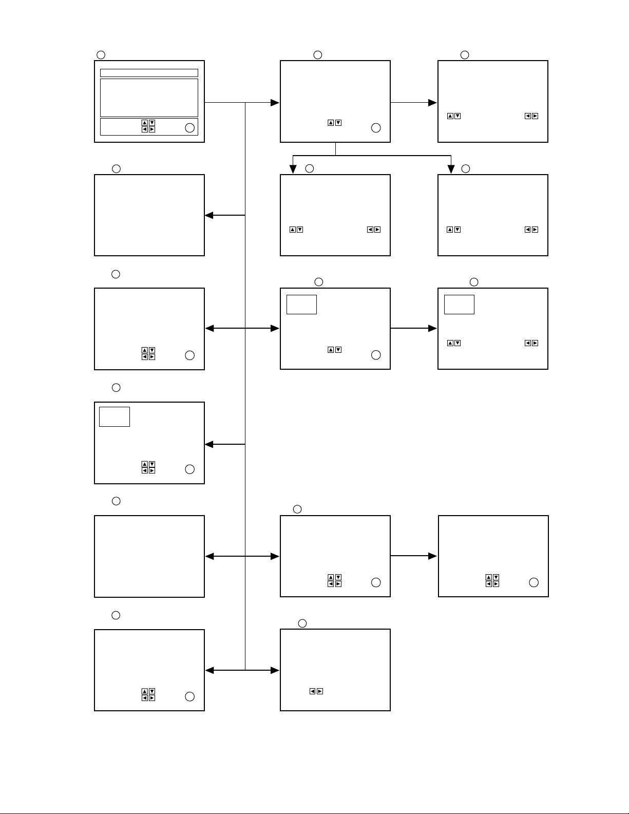
AV-27D502
1
SERVICE MENU (MAIN MENU) SCREEN PICTURE MODE
SERVICE MENU
PICTURE SOUND
THEATER OTHERS
PIP
LOW LIGHT HIGH LIGHT
RF AFC1 RF AFC2
VCO(CW) I2C BUS CTRL
SELECT BY
OPERATE BY
10
HIGH LIGHT MODE
HIGH LIGHT
999 999
11
RF AFC1 MODE
EXIT BY
EX
IT
[DO NOT ADJUST]
TOO HIGH GOOD TOO LOW
RF AFC1 ON
FINE
SELECT BY
OPERATE BY
EXIT BY
999
EX
IT
2
SELECT BY
4
SOUND MODE OTHERS MODE
1. NOISE DET.
STATUS
6
SCREEN PIP MODE
SELECT BY
EXIT BY
999
99999999
EXIT BY
EX
IT
EX
IT
3
1. BRIGHT
STATUS
5
1. OSD POS. 999
1. PIP BR
STATUS
7
999
99999999
999
99999999
12
RF AFC2 MODE
[DO NOT ADJUST]
TOO HIGH GOOD TOO LOW
RF AFC2 ON
FINE
SELECT BY
OPERATE BY
13
VCO (CW) MODE
999
EXIT BY
[DO NOT USE]
HIGH LEVEL
REFERENCE LEVEL
LOW LEVEL
SYNC : YES
14
I2C BUS CTRL MODE
[FIXED ON]
I2C BUS ON
SELECT BY
OPERATE BY
EXIT BY
EX
IT
8
THEATER MODE (1/2) THEATER MODE (2/2)
TINT 999 B CUT. 999
COLOR 999 R DRIVE 999
PICTURE 999 B DRIVE 999
BRIGHT 999 DC REST. 999
DETAIL 999 BLK ST. 999
R CUT. 999 GMM PNT 999
G CUT. 999
SELECT BY
OPERATE BY
9
LOW LIGHT MODE
EX
IT
BRIGHT
999 999
999
EXIT BY
PAGE 1/2
999
EX
IT
CD MAT. 99 CMP CD M 99
RY GAIN 99 CMP RY G 99
GY PHASE 99 CMP GY P 99
CORING 99 CMP COR 99
SELECT BY
OPERATE BY
PAGE 2/2
EXIT BY
EX
IT
No. 51797 15
Page 16
AV-27D502
(4) Setting method
1) UP / DOWN key of the MENU
Select the SETTING ITEM.
2) LEFT / RIGHT key of the MENU
Setting (adjust) the SETTING VALUE of the SETTING ITEM.
When the key is released the SETTING VALUE will be stored (memorized).
3) EXIT key
Returns to the previous screen.
(5) Releasing SERVICE MENU
1) After returning to the SERVICE MENU upon completion of the setting (adjustment) work, press the EXIT key again.
¤ The settings for LOW LIGHT and HIGH LIGHT are described in the WHITE BAL-
ANCE page of ADJUSTMENT.
1. BRIGHT
STATUS
SETTING ITEM
99999999
PICTURE MODE
999
INITIAL
SETTING VALUE
(Adjust)
SETTING VALUE
16 No. 51797
Page 17

AV-27D502
INITIAL SETTING VALUE OF SERVICE MENU
1. Adjustment of the SERVICE MENU is made on the basis of the initial setting values; however, the new setting values which set the
screen in its optimum condition may differ from the initial setting.
2. Do not change the initial setting values of the setting (Adjustment) items not listed in “ADJUSTMENT”.
PICTURE MODE
•
The four setting items in the video mode No.6 EXT BRI., No.7 EXT PIC., No.8 EXT COL. and No.9 EXT TINT are linked to the items in the TV
MODE No.1 BRIGHT, No.2 PICTURE, No.3 COLOR and No.4 TINT, respectively. When the setting items in the TV mode are adjusted, the
values in the setting items in the video mode are revised automatically to the same values in the TV mode.(The initial setting values given in ( )
are off-set values.)
When the four items (No.6, 7, 8 and 9) are adjusted in the video mode, the setting values in each item are revised independently.
No. Setting (Adjustment) item Variable range Initial setting value
1 BRIGHT 000 — 127 063
2 PICTURE 000 — 127 080
3 COLOR 000 — 127 072
4 TINT 000 — 127 065
5 TV DETAIL 000 — 063 045
6 EXT BRIGHT ±025 ±001
7 EXT PICT. ±025 ±002
8 EXT COLOR ±025 ±002
9 EXT TINT ±025 –004
10 EXT DETAIL 000 — 063 045
11 CMP BRIGHT ±025 –003
12 CMP PICT. ±025 +006
13 CMP COLOR 000 — 127 080
14 CMP TINT 000 — 127 068
15 CMP DETAIL 000 — 063 050
16 CMP R CUT ±025 –011
17 CMP G CUT ±025 ±000
18 CMP B CUT ±025 –001
19 CMP R DRV ±025 ±000
20 CMP B DRV ±025 ±000
21 WPL 000 / 001 001
22 B. B. SW 000 / 001 000
23 C TRAP 000 / 001 000
24 CORING 000 / 001 000
25 CMP CORING 000 / 001 001
26 TV SHARPF 000 / 001 001
27 EXT SHARPF 000 / 001 001
28 CMP SHARPF 000 / 001 001
29 RGB CONT 000 — 063 031
30 TV ID SENS 000 / 001 000
31 EXT ID SEN 000 / 001 001
32 F ID 000 / 001 000
33 Y MUTE 000 / 001 000
34 AUDIO ATT 000 — 127 127
35 SUB CONT 000 — 015 008
No. 51797 17
Page 18

AV-27D502
No. Setting (Adjustment) item Variable range Initial setting value
36 R Y GAIN 000 / 001 001
37 CMP R Y GA 000 / 001 001
38 G Y PHASE 000 / 001 000
39 CMP G Y PH 000 / 001 000
40 CD MATRIX 000 — 003 003
41 CMP CD MAT 000 — 003 002
42 BLACK ST 000 — 003 001
43 DC REST 000 — 003 001
44 COLOR GMM 000 / 001 000
45 UV/CBCR 000 / 001 001
46 AT FLESH 000 / 001 000
47 ABL GAIN 000 — 003 000
48 ABL ST PNT 000 — 003 003
49 RGB ABCL 000 / 001 001
50 TV BPF TOF 000 / 001 000
51 EXT BPF TOF 000 / 001 000
52 GMM PNT 000 — 003 003
53 SVM GAIN 000 — 003 003
54 CMP SVM GA 000 — 003 003
55 SVM PHASE 000 / 001 000
56 AUDIO SW 000 / 001 000
57 BUZZ 000 / 001 000
58 IF FREQ 000 / 001 000
59 RF AGC 000 — 063 045
60 AFT MUTE 000 / 001 000
61 AFT SENS 000 / 001 001
62 R/G DRV SW 000 / 001 001
63 BLK SW 000 / 001 000
64 V S COR 000 — 015 012
65 V LIN 000 — 015 007
66 V SIZE 000 — 127 074
67 V AGC 000 / 001 000
68 V CENTER 000 — 063 053
69 TV AFC 000 — 003 000
70 EXT AFC 000 — 003 002
71 V POSI 000 — 007 000
72 H POSI 000 — 031 016
73 H SIZE 000 — 063 023
74 TV V FREQ 000 — 003 000
75 EXT V FREQ 000 — 003 003
76 SIDE PIN 000 — 063 027
77 STAND BY 000 / 001 000
78 TRAPEZ 000 — 063 035
79 V RAMP REF 000 / 001 001
80 V 48HZ 000 / 001 000
81 V EHT 000 — 007 000
82 TOP PIN 000 — 031 010
18 No. 51797
Page 19

AV-27D502
No. Setting (Adjustment) item Variable range Initial setting value
83 H EHT 000 — 007 000
84 BTM PIN 000 — 031 012
85 V BLK LOW 000 — 003 000
86 V BLK UP 000 — 003 000
87 CAPTION IN 000 / 001 000
88 H BLK 000 / 001 000
89 SCREEN 000 / 001 000
90 ACB SW 000 / 001 000
91 ACB PULSE 000 — 015 007
92 OVER MODU 000 / 001 001
93 APACON LIM 000 / 001 001
94 TEST 000 — 255 128
95 RF S/N TY 000 — 002 002
96 EXT S/N TY 000 — 002 002
97 RF SN YC E 000 — 255 005
98 RF SN YC F 000 — 255 016
99 RF SN YC G 000 — 063 032
100 RF SN YC H 000 — 255 025
101 EX SN YC E 000 — 255 005
102 EX SN YC F 000 — 255 016
103 EX SN YC G 000 — 063 032
104 EX SN YC H 000 — 255 025
105 RF SN VC 1 000 — 063 000
106 RF SN VC 2 000 — 063 007
107 RF SN VC 3 000 — 063 014
108 RF SN VC 4 000 — 063 021
109 EX SN VC 1 000 — 063 000
110 EX SN VC 2 000 — 063 007
111 EX SN VC 3 000 — 063 014
112 EX SN VC 4 000 — 063 021
113 COR LEVEL 000 — 003 003
114 VNR CHK 000 — 255 003
115 YC SN TIME 000 — 255 005
116 VC SN TIME 000 — 255 005
117 VM DATA A ±127 +008
118 VM DATA B ±127 –004
119 VM DATA C ±127 –016
120 VM DATA D 000 / 001 000
121 VC SN STOP 000 — 255 010
122 CH MUTE 00/001 000
123 VM OFF TY 000/001 000
124 VC VM OFF 000/001 001
125 YC VM OFF 000 — 255 255
126 F LOCK 000 — 002 002
127 VF LOCK EX 000/001 000
128 PURI RGB 000 — 063 031
129 PURI BCK 000/001 000
No. 51797 19
Page 20

AV-27D502
SOUND MODE
•
No. Setting (Adjustment) item Variable range Initial setting value
1 NOISE DET. 000 / 001 001
2 IN LEVEL 000 — 063 025
3 FH MONITOR 000 / 001 000
4 STEREO VCO 000 — 063 030
5 PILOT CAN. 000 / 001 000
6 FILTER 000 — 063 030
7 LOW SEP. 000 — 063 028
8 HI SEP. 000 — 063 025
9 5FH MON. 000 / 001 000
10 SAP VCO 000 — 063 003
11 IN GAIN 000 / 001 000
12 FIL. OFFSET ±010 ±000
13 BBE BASS ±010 +003
14 BBE TRE ±010 +003
THEATER MODE
•
Setting (Adjustment) item Variable range Initial setting value
TINT ±20 –06
COLOR ±20 –03
PICTURE ±50 –15
BRIGHT ±20 ±00
DETAIL ±20 +03
R CUT. ±20 ±00
G CUT. ±20 ±00
B CUT. ±20 ±00
R DRIVE ±99 +07
B DRIVE ±99 –25
DC REST. 00 — 03 01
BLK ST. 00 — 03 00
GMM PNT 00 — 03 01
CD MATRIX 00 — 03 01
RY GAIN 00 / 01 01
GY PHASE 00 / 01 00
CORING 00 / 01 01
CMP CD M 00 — 03 01
CMP RY G 00 / 01 01
CMP GY P 00 / 01 00
CMP COR 00 / 01 01
20 No. 51797
Page 21

AV-27D502
OTHERS MODE
•
No. Setting (Adjustment) item Variable range Initial setting value
1 OSD POS. 000 — 007 002
2 CCD POS. 000 — 015 003
3 EOSEL 000 / 001 000
4 MENU COLOR 000 — –030 –010
5 MENU PICT. 000 — –030 –010
6 MENU BRI. 000 — –030 –010
PIP MODE
•
No. Setting (Adjustment) item Variable range Initial setting value
1 PIP BR 000 — 015 005
2 PIP PICT 030 — 045 045
3 PIP TINT 000 — 063 036
4 PIP COL 000 — 015 010
5 P R CUT 000 — 015 003
6 P G CUT 000 — 015 000
7 P B CUT 000 — 015 002
8 P R DR 000 — 255 052
9 P G DR 000 — 255 055
10 P B DR 000 — 255 060
11 LEFT POS. 000 — 255 020
12 RIGHT POS. 000 — 255 017
13 UPPER POS. 000 — 127 012
14 LOWER POS. 000 — 127 011
15 PICT LOCK 000 / 001 001
16 SELDEL 000 — 015 000
17 AGCFIX 000 / 001 001
18 AGCADST 000 / 001 000
19 AGC 000 — 015 007
20 VSPDEL 000 — 031 000
21 VSPISQ 000 / 001 001
22 YCOR 000 / 001 001
23 XFREQF 000 / 001 001
24 WTCHDG 000 / 001 001
25 COLON 000 / 001 000
26 ACQNEW 000 / 001 000
27 DSTDET 000 / 001 001
28 CRIBEOK 000 / 001 000
29 FCBEOK 000 / 001 000
30 NOCRID 000 / 001 000
31 NONSED 000 / 001 000
No. 51797 21
Page 22
AV-27D502
LOW LIGHT MODE
•
Setting (Adjustment) item Variable range Initial setting value
R CUTOFF 0 — 255 085
G CUTOFF 0 — 255 085
B CUTOFF 0 — 255 085
HIGH LIGHT MODE
•
Setting (Adjustment) item Variable range Initial setting value
R DRIVE 0 — 127 060
B DRIVE 0 — 127 060
RF AFC1 MODE
•
Setting (Adjustment) item Variable range Initial setting value
RF AFC1 ON / OFF ON
FINE -77 — +77 ± × ×
RF AFC2 MODE
•
Setting (Adjustment) item Variable range Initial setting value
RF AFC2 ON / OFF ON
FINE -77 — +77 ± × ×
I2C BUS CTRL MODE
•
Setting (Adjustment) item Variable range Initial setting value
I2C BUS ON/OFF [FIXED ON]
DO NOT
ADJUST
DO NOT
ADJUST
DO NOT
ADJUST
22 No. 51797
Page 23
ADJUSTMENTS
B1 POWER SUPPLY
Item
Measuring
instrument
AV-27D502
Test point Adjustment part Description
Check of
B1 POWER
SUPPLY
DC Voltmeter R507 C504
ADJUSTMENT OF RF AGC
Item
RF AGC
adjustment
Measuring
instrument
1. Receive a black-and-white signal.
side (B1)
Q511
heatsink ( )
Test point Adjustment part Description
No.59 RF AGC
2. Connect the DC Voltmeter to R507 C504 side (B1) and Q511 heatsink
( ).
3. Confirm that the voltage is DC134V .
1. Receive a broadcast.
2. Select the No.59 RF AGC of the PICTURE MODE.
3. Press the MUTE key of the remote control unit and turn off color.
4. With the LEFT key of the remote control unit, get noise in the screen
picture. (0 side of setting value)
5. Press the RIGHT key of the remote control unit and stop when noise
disappears from the screen.
6. Change to other channels and make sure that there Is no irregularity.
7. Press the MUTE key and get color out.
+2V
-2V
ADJUSTMENT OF FOCUS
Item
FOCUS
adjustment
Measuring
instrument
Signal
generator
Test point Adjustment part Description
FOCUS VR
[In HVT]
H VR
[In HVT]
Notes:
• Proceed to the following this adjustment after having completed the
adjustments of B1 POWER SUPPLY, SUB BRIGHT and PICTURE.
• Set VIDEO STATUS to “STANDARD”.
• The final adjustment of convergence must be done after the FOCUS
adjustment. (Convergence is changed by FOCUS adjustment.)
1. Receive a crosshatch signal.
2. While looking at the screen center, adjust the FOCUS VR so that
the horizontal lines will be clear and in fine detail.
3. Adjust the H VR so that the vertical lines will be clear and in fine
detail.
4. Make sure that the picture is in focus even when the screen gets
darkened.
No. 51797 23
Page 24
AV-27D502
ADJUSTMENT OF WHITE BALANCE
Item
Measuring
instrument
Test point Adjustment part
Description
WHITE
BALANCE
(Low Light)
Adjustment
Signal
generator
[LOW LIGHT] MODE
BRIGHT
999
R CUTOFF
REMOTE CONTROL UNIT
H.LINE ON
999
999 999
G CUTOFF
H.LINE OFF EXIT
123
R CUTOFF G CUTOFF B CUTOFF
456
R CUTOFF G CUTOFF B CUTOFF
789
No.1 BRIGHT
R CUTOFF
G CUTOFF
B CUTOFF
SCREEN VR
[In HVT]
BRIGHT
B CUTOFF
Note :
Set VIDEO STATUS to “STANDARD”.
1. Receive a black-and-white signal.(Color off)
2. Select the [LOW LIGHT] MODE from the SERVICE MENU.
3. Set the initial setting value of BRIGHT is 063 with the LEFT / RIGHT
key of the remote control unit.
4. Set the initial setting value of R CUTOFF, G CUTOFF and B CUTOFF is 085 with the 4 to 9 key of the remote control unit.
5. Display a single horizontal line by pressing the 1 key of the remote
control unit.
6. Turn the screen VR all the way to the left.
7. Turn the screen VR gradually to the right from the left until either
one of the red, blue or green colors appears faintly.
8. Adjust the two colors which did not appear until the single horizontal
line that is displayed becomes white using the 4 to 9 keys of the
remote control unit.
9. Turn the screen VR to where the single horizontal line glows faintly.
10.Press the 2 key to return to the regular screen.
9 The 3 EXIT key is the cancel key for the WHITE BALANCE.
WHITE
BALANCE
(High Light)
Adjustment
Signal
generator
[HIGH LIGHT] MODE
999
R DRIVE
REMOTE CONTROL UNIT
H.LINE ON
HIGHT LIGHT
H.LINE OFF EXIT
999
123
R DRIVE B DRIVE
456
R DRIVE B DRIVE
789
R DRIVE
B DRIVE
B DRIVE
Notes:
• Proceed to the following this adjustment after having completed the
adjustment of LOW LIGHT WHITE BALANCE.
• Set VIDEO STATUS to “STANDARD”.
1. Receive a black-and-white signal. (Color off)
2. Select the [HIGH LIGHT] MODE from the SERVICE MENU.
3. Set the initial setting value of R DRIVE and B DRIVE is 060 with the
4 , 6 , 7 and 9 keys of the remote control unit.
4. Adjust the screen until it becomes white using the 4 , 6 , 7 and 9
keys of the remote control unit.
9 The 3 (EXIT) key is the cancel key for the WHITE BALANCE.
24 No. 51797
Page 25
AV-27D502
Item
PIP
HIGH LIGHT
WHITE
BALANCE
Measuring
instrument
Signal
generator
ADJUSTMENT OF BRIGHT
Item
SUB BRIGHT
Adjustment
Measuring
instrument
Test point Adjustment part Description
No.8 P R DR
No.10 P B DR
PIP screen
Main screen
Test point Adjustment part Description
No.1 BRIGHT Notes:
Notes:
• Proceed to the following this adjustment after having completed the
adjustments of LOW LIGHT WHITE BALANCE and HIGH LIGHT
WHITE BALANCE for the main picture.
• Set VIDEO STATUS to “STANDARD”.
1. Receive a black-and-white signal. (Color off)
2. Select the PIP MODE from the SERVICE MENU.
3. Then adjust the white color of the PIP screen using the No. 8 P R
DR and the No. 10 P B DR of the PIP MODE so that it is the same
brightness as the main screen.
• Proceed to the following this adjustment after having completed the
adjustments of LOW LIGHT WHITE BALANCE and HIGH LIGHT
WHITE BALANCE.
• Set VIDEO STATUS to “STANDARD”.
ADJUSTMENT OF CONTRAST
Item
SUB
CONTRAST
Adjustment
Measuring
instrument
Test point Adjustment part Description
No.2 PICTURE
1. Receive a broadcast.
2. Select the No.1 BRIGHT of the PICTURE MODE.
3. Set the initial setting value of the No.1 BRIGHT with the LEFT /
RIGHT key of the remote control unit.
4. If the brightness is not best with the initial setting value, make fine
adjustment of the No.1 BRIGHT until you get the optimum brightness.
Notes:
• Proceed to the following this adjustment after having completed the
adjustment of SUB BRIGHT.
• Set VIDEO STATUS to “STANDARD”.
1. Receive a broadcast.
2. Select the No.2 PICTURE of the PICTURE MODE.
3. Set the initial setting value of the No.2 PICTURE with the LEFT /
RIGHT key of the remote control unit.
4. If the contrast is not best with the initial setting value, make fine
adjustment of the No.2 PICTURE until you get the optimum contrast.
No. 51797 25
Page 26
AV-27D502
ADJUSTMENT OF DEFLECTION
Item
Measuring
instrument
Test point Adjustment part Description
V CENTER and
TRAPEZIUM
Adjustment
V-SIZE and
V-LINEARITY
Adjustment
Screen
size 90%
Signal
generator
Signal
generator
Screen size
No.68 V CENTER
No.78 TRAPEZ
No.66 V SIZE
No.65 V LIN
Picture
size 100%
Note:
Proceed to the following this adjustment after having completed the
adjustments of SUB BRIGHT and SUB CONTRAST.
1. Receive a crosshatch signal.
2. Adjust the No.68 V CENTER of the PICTURE MODE to be the same
between the CRT vertical center and crosshatch vertical center.
3. Adjust the No.78 TRAPEZ of the PICTUER MODE to be the vertical
lines straight.
4. Confirm the vertical lines to be straight. If it is not straight, adjust to
be straight at the No.78 TRAPEZ.
Note:
Proceed to the following this adjustment after having completed the
adjustments of SUB BRIGHT and SUB CONTRAST.
1. Receive a crosshatch signal.
2. Select the No.66 V SIZE of the PICTURE MODE to squeeze the
laster.
3. Adjust the No.65 V LIN of the PICTURE MODE to be symmetrical.
4. Adjust the No.66 V SIZE until the vertical screen size is 90%.
H POSITION
Adjustment
PIP DISPLAY
POSITION
Adjustment
UPPER POS.
LOWER POS.
Picture size 100%
Signal
generator
LEFT POS. RIGHT POS.
No.72 H POSI
No.11 LEFT POS.
No.12 RIGHT POS.
No.13 UPPER POS.
No.14 LOWER POS.
80%
±2%
Main
screen
size
Note:
Proceed to the following this adjustment after having completed the
adjustments of FOCUS, SUB BRIGHT, SUB CONTRAST, V CENTER,
TRAPEZIUM, V-SIZE and V-LINEARITY.
1. Receive a crosshatch signal.
2. Select the No.72 H POSI of the PICTURE MODE.
3. Adjust the No.72 H POSI until the screen will be horizontally centered.
Notes:
• Proceed to the following this adjustment after having completed the
adjustments of V CENTER, TRAPEZIUM, V-SIZE, V-LINEARITY and
H POSITION for the main picture.
• Set VIDEO STATUS to “STANDARD”.
1. Receive a broadcast.
2. Select the PIP MODE from the SERVICE MENU.
3. Then adjust the PIP screen size so that it occupies 80% ± 2% of the
main screen area.
80% ±2%
Main screen size
26 No. 51797
Page 27
ADJUSTMENT OF CHROMA
Item
Measuring
instrument
AV-27D502
Test point Adjustment part Description
SUB COLOR
adjustment
Signal
generator
Oscilloscope
Remote
control unit
Y
Cy
W
TP-B
TP-E(
No.3 COLOR
)
[CRT SOCKET
PWB]
G
R
(A)
(–)
0V
B
Mg
AV-27D502/R +7V
AV-27D502/S +4V
(+)
A (Vw-B)
Table 1
Notes:
• Proceed to the following this adjustment after having completed the
adjustment of CONTRAST.
• Set VIDEO STATUS to “STANDARD”.
[ Method of adjustment without measuring instrument ]
1. Receive a broadcast.
2. Select the No.3 COLOR of the PICTURE MODE.
3. Set the initial setting value of the No.3 COLOR with the LEFT/RIGHT
key of the remote control unit.
4. If the color is not the best with the Initial setting value, make fine
adjustment of the No.3 COLOR until you get the optimum color.
Notes:
• Proceed to the following this adjustment after having completed the
adjustment of CONTRAST.
• Set VIDEO STATUS to “STANDARD”.
[ Method of adjustment using measuring instrument ]
1. Input the full field color bar signal (75% white).
2. Select the No.3 COLOR of the PICTURE MODE.
3. Set the initial setting value of the No.3. COLOR with the LEFT/RIGHT
key of the remote control unit.
4. Connect the oscilloscope between TP-B and TP-E.
5. Adjust COLOR and bring the value of (A) in the illustration to the
voltage shown in the table 1.
SUB TINT
adjustment
Signal
generator
Oscilloscope
Remote
control unit
Y
Cy
W
TP-B
No.4 TINT
TP-E( )
[CRT SOCKET
PWB]
G
R
(–)
0V
Mg
B
(+)
(B)
AV-27D502/R +9V
AV-27D502/S +5V
B (Vw-Mg)
Table 2
Notes:
• Proceed to the following this adjustment after having completed the
adjustment of CONTRAST.
• Set VIDEO STATUS to “STANDARD”.
[ Method of adjustment without measuring instrument ]
1. Receive a broadcast.
2. Select the No.4 TINT of the PICTURE MODE.
3. Set the initial setting value of the No.4 TINT with the LEFT/RIGHT
key of the remote control unit.
4. If the tint is not the best with the initial setting value, make fine ad-
justment of the No.4 TINT until you get the optimum tint.
Notes:
• Proceed to the following this adjustment after having completed the
adjustment of CONTRAST.
• Set VIDEO STATUS to “STANDARD”.
[ Method of adjustment using measuring instrument ]
1. Input the full field color bar signal (75% white).
2. Select the No.4 TINT of the PICTURE MODE.
3. Set the initial setting value of the No.4 TINT with the LEFT/RIGHT
key to the remote control unit.
4. Connect the oscilloscope between TP-B and TP-E.
5. Adjust TINT and bring the value of (B) in the illustration to the volt-
age shown in the table 2.
No. 51797 27
Page 28
AV-27D502
ADJUSTMENT OF MTS CIRCUIT
Item
Measuring
instrument
Test point Adjustment part Description
MTS INPUT
LEVEL
check
MTS STEREO
VCO
adjustment
MTS SAP
VCO
adjustment
Signal
generator
Frequency
counter
Signal
generator
Frequency
counter
[MPX]
Connector
2
pin AUDIO R
3 pin GND
[MPX]
Connector
4 pin TP_952.5
3 pin GND
2 pin AUDIO_R
No.2 IN LEVEL
No.3 FH MONITOR
No.4 STEREO VCO
No.9 5FH MON.
No.10 SAP VCO
1. Select the No.2 IN LEVEL of the SOUND MODE.
2. Verify that the No.2 IN LEVEL is set at its initial setting value.
Note: Menu “MTS” is set to “STEREO”
1. Receive a RF signal (nonmodulated sound signal) from the antenna
terminal.
2. Select the No.3 FH MONITOR of SOUND MODE, and change the
setting value from 0 to 1.
3. Connect the Frequency Counter to pin 2 of [MPX] connector and
GND (Pin 3 of [MPX] connector).
4. Select the No.4 STEREO VCO.
5. Set the initial setting value of the No.4 STEREO VCO with the LEFT/
RIGHT key of the remote control unit.
6. Adjust the No.4 STEREO VCO so that the frequency counter will
display 15.73kHz±0.1kHz.
7. Select the No.3 FH MONITOR of the SOUND MODE, and reset the
setting value from 1 to 0.
1. Receive a RF signal (non modulated sound signal) from the antenna terminal.
2. Connect between pin 4 of [MPX] connector and GND (Pin 3 of [MPX]
connector) through 1MØ Resistor.
3. Select the No.9 5FH MON. of the SOUND MODE, and reset the
setting value from 0 to 1.
4. Connect the Frequency Counter to pin 2 of [MPX] connector and
GND (Pin 3 of [MPX] connector) .
5. Select the No.10 SAP VCO.
6. Set the initial setting value of the No.10 SAP VCO with the LEFT/
RIGHT key of the remote control unit.
7. Adjust the No.10 SAP VCO so that the frequency counter will display 78.67kHz±0.5kHz.
8. Select the No.9 5FH MON. of the SOUND MODE, and reset the
setting value from 1 to 0.
MTS FILTER
check
MTS
SEPARATION
adjustment
L-Channel
signal waveform
1 cycle
TV audio
multiplex
signal
generator
Oscilloscope
[MPX]
Connector
1 pin AUDIO_L
2 pin AUDIO_R
3 pin GND
R-Channel
crosstalk portion
Minimum
No.6 FILTER
No.7 LOW SEP.
No.8 HI SEP.
1. Select the No.6 FILTER of the SOUND MODE.
2. Verify that the No.6 FILTER is set at its initial setting value.
Note: Menu “MTS” is set to “STEREO”
1. Input a stereo L signal (300Hz) from the TV audio multiplex signal
2. Connect an oscilloscope to pin 1 of [MPX] connector, and display
3. Change the connection of the oscilloscope to pin 2 of [MPX] con-
4. Select the No.7 LOW SEP. of the SOUND MODE.
5. Set the initial setting value of the No.7 LOW SEP. with the LEFT/
6. Adjust the No.7 LOW SEP. so that the 300Hz signal level will be-
7. Change the signal to 3kHz, and connect an oscilloscope to pin 1 of
8. Adjust the No.8 HI SEP. so that the 3kHz signal level will become
28 No. 51797
generator to the antenna terminal.
one cycle portion of the 300Hz signal.
nector, and enlarge the voltage axis.
RIGHT key of the remote control unit.
come minimum.
[MPX] connector.
minimum.
Page 29
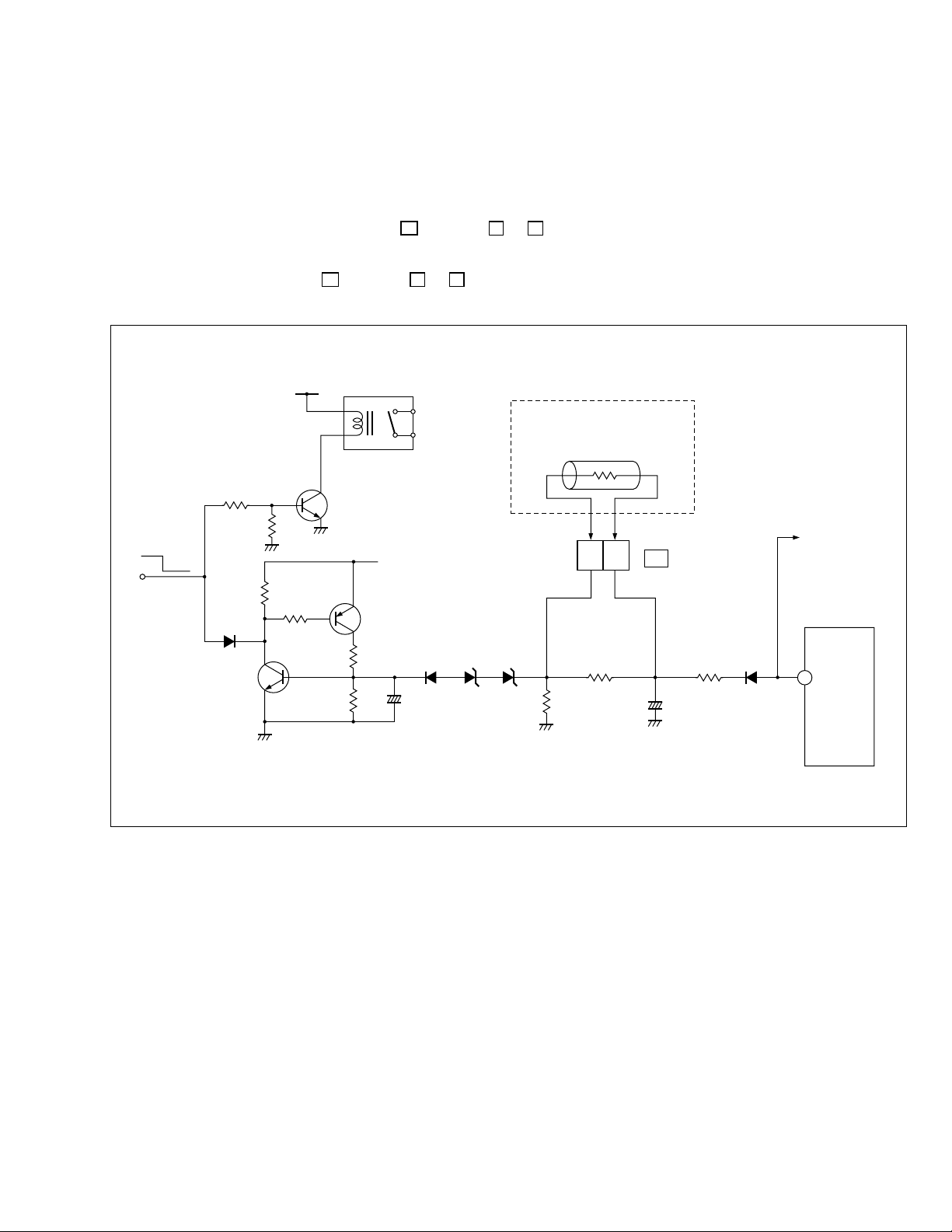
HOW TO CHECK THE HIGH VOLTAGE HOLD DOWN CIRCUIT
1. HIGH VOLTAGE HOLD DOWN CIRCUIT
After repairing the high voltage hold down circuit shown in Fig. 1.
This circuit shall be checked to operate correctly.
2. CHECKING OF THE HIGH VOLTAGE HOLD DOWN CIRCUIT
(1) Turn the POWER SW ON.
S1
(2) As shown in Fig. 1, set the resistor (between
(3) Make sure that the screen picture disappears.
(4) Temporarily unplug the power cord.
(5) Remove the resistor (between S1 connector 2 & 3 ).
(6) Again plug the power cord, make sure that the normal picture is displayed on the screen.
RY951
connector 2 & 3 ).
RESISTOR
24.5 kΩ ± 122 Ω 1/4 W
AV-27D502
POWER
ON OFF
R952
R532
D535
R951
R533
Q531
Q951
Q532
R534
+
C533
D534
D532
BW
D531
Fig. 1
23
R537 FR525
R535R538
S1 CONNECTOR
+
HEATER
T502
4
D525
C525
No. 51797 29
Page 30

AV-27D502
SELF CHECK FUNCTIONS
1. Outline
This model has self check functions given below. When a malfunction has been detected, the POWER is turned off and the LED flashes to inform
of the failure . The malfunction is detected by the signal input state of the control line connected to the microcomputer.
2. Self check items
Check item Details of detection Method of detection State of malfunction
Over-current protector
3. Self check indicating function
The self-check function begins detection about 5 seconds after power
is supplied.
In the event a malfunction is detected, the power is cut off immediately.
At this time, the ON-TIMER LED flashes to inform of the malfunction.
[ON-TIMER LED indication]
The ON-TIMER LED flashes at 0.5 seconds intervals.
Operation of B1 protector circuit. The microcomputer detects at 1
second intervals.
If NG is detected for more than
200 ms, a malfunction is interpreted.
POWER
Supplied
After about
5 seconds
Start of
detection
When a malfunction has been
detected, the POWER is turned
off. While the POWER is being
turned off , the power key of the
remote controller is not operational until the power code is
taken out and put in again.
Malfunction
is detected
POWER OFF
Flashing
ON-TIMER LED
30 No. 51797
Page 31

JVC SERVICE & ENGINEERING COMPANY OF AMERICA
DIVISION OF JVC AMERICAS CORP.
Head office :
East Coast :
Midwest :
West Coast : 5665 Corporate Avenue, Cypress, California 90630 (714)229-8011
Southwest : 10700 Hammerly, Suite 105, Houston, Texas 77043 (713)935-9331
Hawaii : 2969 Mapunapuna Place, Honolulu, Hawaii 96819 (808)833-5828
Southeast : 1500 Lakes Parkway, Lawrenceville, Georgia 30243 (770)339-2582
1700 Valley Road, Wayne, New Jersey 07470 (973)315-5000
10 New Maple Avenue, Pine Brook, New Jersey 07058 (973)396-1000
705 Enterprise St. Aurora, Illinois 60504
(630)851-7855
JVC CANADA INC.
Head office : 21 Finchdene Square Scarborough, Ontario M1X 1A7 (416)293-1311
Vancouver : 13040 Worster Court Richmond B.C. V6V 2B3 (604)270-1311
®
AV27D502R-UCM #4
AV27D502S-UCM #2
Printed in Japan
VP0103
SW
Page 32

AV-27D502
SCHEMATIC DIAGRAMS
COLOR TELEVISION
BASIC CHASSIS
GC
AV-27D502
AV-27D502
CD-ROM No. SML200201
/AR
/AS
TV
COPYRIGHT © 2001 VICTOR COMPANY OF JAPAN, LTD.
No. 51797C
Dec. 2001
Page 33

AV-27D502
AV-27D502 /AR AV-27D502 /AS STANDARD CIRCUIT DIAGRAM
q
NOTE ON USING CIRCUIT DIAGRAMS
1. SAFETY
The components identified by the symbol and shading are
critical for safety. For continued safety replace safety critical
components only with manufactures recommended parts.
2. SPECIFIED VOLTAGE AND WAVEFORM VALUES
The voltage and waveform values have been measured under the
following conditions.
(1) Input signal : Color bar signal
(2)
Setting positions of each knob/button and
variable resistor
(3) Internal resistance of tester : DC 20kØ/V
(4) Oscilloscope sweeping time : H ⇒ 20µS/div
(5) Voltage values : All DC voltage values
: Original setting position when
shipped
:V ⇒ 5mS/div
: Others ⇒ Sweeping time is
specified
9Since the voltage values of signal circuit vary to some extent ac-
cording to adjustments, use them as reference values.
3. INDICATION OF PARTS SYMBOL [EXAMPLE]
•In the PW board : R1209
→
R209
Type
•
No indication : Ceramic capacitor
MY : Mylar capacitor
MM : Metalized mylar capacitor
PP : Polypropylene capacitor
MPP : Metalized polypropylene capacitor
MF : Metalized film capacitor
TF : Thin film capacitor
BP : Bipolar electrolytic capacitor
TAN : Tantalum capacitor
(3) Coils
No unit : [µH]
Others : As specified
(4) Power Supply
:B1
: B2(12V)
:9V
:5V
9Respective voltage values are indicated
(5) Test point
: Test point
: Only test point display
4. INDICATIONS ON THE CIRCUIT DIAGRAM
(1) Resistors
Resistance value
•
No unit : [Ø]
k:[kØ]
M:[MØ]
Rated allowable power
•
No indication : 1/16 [W]
Others : As specified
Type
•
No indication : Carbon resistor
OMR : Oxide metal film resistor
MFR : Metal film resistor
MPR : Metal plate resistor
UNFR : Uninflammable resistor
FR : Fusible resistor
9Composition resistor 1/2 [W] is specified as 1/2S or Comp.
(2) Capacitors
Capacitance value
•
1 or higher : [pF]
less than 1 : [µF]
Withstand voltage
•
No indication : DC50[V]
AC indicated : AC withstand voltage [V]
Others : DC withstand voltage [V]
9 Electrolytic Capacitors
47/50[Example] : Capacitance value [µF]/withstand voltage[V]
(6) Connecting method
: Connector
: Wrapping or soldering
: Receptacle
(7) Ground symbol
: LIVE side ground
: ISOLATED(NEUTRAL) side ground
: EARTH ground
: DIGITAL ground
5. NOTE FOR REPAIRING SERVICE
This model’s power circuit is partly different in the GND. The difference
of the GND is shown by the LIVE : ( ) side GND and the
ISOLATED(NEUTRAL) : ( ) side GND. Therefore, care must be taken
for the following points.
(1) Do not touch the LIVE side GND or the LIVE side GND and the
ISOLATED(NEUTRAL) side GND simultaneously. If the above caution is not respected, an electric shock may be caused. Therefore,
make sure that the power cord is surely removed from the receptacle when, for example, the chassis is pulled out.
(2) Do not short between the LIVE side GND and ISOLATED(NEUTRAL)
side GND or never measure the LIVE side GND and
ISOLATED(NEUTRAL) side GND at the same time with a measuring apparatus ( oscilloscope, etc.). If the above precaution is not
respected , a fuse or any parts will be broken.
Since the circuit diagram is a standard one, the circuit and cir-
•
cuit constants may be subject to change for improvement without any notice.
Dec. 2001 No. 51797C
Page 34

AV-27D502
CONTENTS
SEMICONDUCTOR SHAPES............................................................................................................................ 2-2
BLOCK DIAGRAM ...................................................................................................................................................... 2-3
CIRCUIT DIAGRAMS................................................................................................................................................ 2-5
MAIN PWB CIRCUIT DIAGRAM (1/3)
MAIN PWB CIRCUIT DIAGRAM (2/3)
MAIN PWB CIRCUIT DIAGRAM (3/3)
AV SELECTOR PWB CIRCUT DIAGRAM
PIP PWB CIRCUIT DIAGRAM
.................................................................................................................................... 2-13
CRT SOCKET PWB CIRCUIT DIAGRAM
FRONT CONTROL AND FRONT AV INPUT PWB CIRCUIT DIAGRAMS
PATTERN DIAGRAMS ........................................................................................................................................... 2-17
MAIN PWB PATTERN
AV SELECTOR PWB PATTERN
CRT SOCKET PWB PATTERN
PIP PWB PATTERN
FRONT CONTROL AND FRONT AV INPUT PWB PATTERNS
.................................................................................................................................................... 2-17
.................................................................................................................................. 2-21
........................................................................................................................................................ 2-22
....................................................................................................................... 2-5
....................................................................................................................... 2-7
....................................................................................................................... 2-9
............................................................................................................. 2-11
.............................................................................................................. 2-15
.................................................. 2-16
................................................................................................................................ 2-19
...................................................................... 2-23
CHANNEL CHART (US)....................................................................................................................................... 2-25
CHANNEL CHART (CA) ...................................................................................................................................... 2-26
SEMICONDUCTOR SHAPES
TRANSISTOR
TOP VIEWBOTTOM VIEW FRONT VIEW
CHIP TR
C
B
E
TOP VIEWBOTTOM VIEW FRONT VIEW
1N
IC
E
C
B
ECB
OUT
E
IN
IN E OUT
EC
B
(G)(D)(S)
ECB
1N
ECB
1N
CHIP IC
TOP VIEW
N
N
N
1
N
2-2 No.51797C
1
N
Page 35

BLOCK DIAGRAM
AV-27D502
AV-27D502
VIDEO/Y
J601
COMPONENT
VIDEO-IN
PB
PR
SCL0
SDA0
TU001
TUNER
PIP PWB
AV SELECTOR PWB (1/2)
S-VIDEO
J501
INPUT1
J502
INPUT2
J503
AUDIO OUT
VIDEO
AUDIO L/MONO
AUDIO R
S-VIDEO
AUDIO L/MONO
AUDIO R
AUDIO L
AUDIO R
TU001
TUNER
IF
Y1,C1
V1
Y2,C2
IF R, G, B
SCL0
SDA0
IC101
IF DET
V-PIP(TV)
Y1
C1
V1
Y2
C2
V3
V1
V3
Y1
C1
Y2
C2
L1/R1
L2/R2
L3/R3
AFT2
+
+
SCL0,SDA0
Q501,Q502
V
AMP
Q503,Q504
V
AMP
IC501
VIDEO
SEL.
IC503
SW.
IC381
SW.
IC301
PIP
CONTROLLER
V-PIP(EXT.)
IC502
VIDEO
SEL.
VTV
VIDEO
Y
C
EL1/ER1
HP
VP
Q211,Q212
BPF
IC504
SW.
VIDEO/Y
C
Y
C
Y
IC201
3L DIGITAL
COMB FILTER
IC371
AMP
SCL0
SDA0
COM_Y
COM_CB
COM_CR
VC_R
VC_G
VC_B
VC_YS
C
Y
OSDR,OSDG,OSDB,OSDYS
IC702
EEPROM
Y
C
LPF
BPF
IC101
1 CHIP DECODER
AMP
BUF
HP,VP
AFT2
SCL1
SDA1
IF
SIF
MPX
V. OUT
H. OUT
Y
C
SCL0
SDA0
IC701
MICRO
COMPUTER
CF021
4.5MHz
TRAP
CF041
4.5MHz BPF
VTV
MAIN PWB
S421
V. CENTER SW
IC421
VERT OUT
Q511
H. OUT
CNMPX
L/R
SCL0
SDA0
EL1/ER1
CRT SOCKET PWB
RGB DRIVE
AUDIO_L/R
AV SELECTOR PWB (2/2)
IC001
MTS&
TONE/VOL
CONTROL
L3/R3
R, G, B
ENHANCEMENT
PROCESSOR
L/R
AUDIO OUT
IC151
SOUND
AUDIO
IC621
V01
L/R
SP
L
SP
R
V
H
DY01
DEF YOKE
FRONT AV INPUT PWB
J401-J403
INPUT3
(FRONT)
VIDEO
AUDIO L/MONO
AUDIO R
V3
FRONT CONTROL PWB
VOL+
POWER
REMOCON
RECEIVER
VOL- CH+ CH- MENU
ON TIMER
LED
AC IN
120V/60Hz
2-3No.51797C
REG.
POWER SUPPLY
CIRCUIT
2-4 No.51797C
B1
T502
FBT
FOCUS
SCREEN
HV
Page 36

CIRCUIT DIAGRAMS
MAIN PWB CIRCUIT DIAGRAM (1/3)
MAIN PWB ASS'Y
SGC-1002A-M2
(AV-27D502
SGC-1001A-M2
(AV-27D502
J601
QNN0349-002
Y
LC601
QQR1199-001
INPUT-2
(COMPONENT
VIDEO INPUT)
VTV
MPX
Y002
Y003
0
Pb
Pr
0
LC001
J601
LC602
QQR1199-001
LC603
QQR1199-001
X
8.8V
Q024
C030
∗1
0.01
2.2V
1.6V
R038
2.7k
ANT INPUT
AGC
R001
47k
C001
4.7/50
/AR)
/AS)
C601
R601
47/25
75
R602
47/25
75
47/25
R603
75
!!TU001
QAU0247-001
4.0V
6.8V
4.8V
TU NC
R002
0
XC005
AGC_MUTE
C602
C603
330R003
SCL0
2.6V
330R004
SDA0
2.6V
1000/16
C003
D605
BW
D604
BW
TUNER
Y004
C006
X
D602
BW
X
4.9V
0R610
∗4D606
0R611
∗4D603
0R612
∗4D601
R028
820
QAX0639-001Z
4.5MHzTRAP
31.2V
BTNC
C002
10/50
56
L001
R026
330
L022
CF021
IF5V LOCKSCL SDAADRS
QQL244K-560Z
QQL244K-220Z
22
0V
CF001
QAX0349-001
COM_CR
560R025
R043
1k
47p CH
C048
0.01
CF041
QAX0642-001Z
4.5MHzBPF
L041
QRN143J-0R0X
C036
470/10
C044
QQL244K-220Z
0
C045
10/50
COM_CB
C043
47p CH
R042
L042
22
R041
2.7k
QRN143J-0R0X
C011
0.01
X
L011
42
IC101
(H)
0.66Vp-p
47
IC101
(H)
0.8Vp-p
COM_Y/CV
()
COM_Y
R020
3.3k
Q021
8.8V
∗1
5.2V
R023
100
4.6V
R024
1k
1k
3.7V
3.1V
Q041
∗2
L021
C024
0
0.01
QRE121J-101Y
R013
5.6k
R011
82
L012
0.39QQLZ014-R39
R014
100
8.9V
Q011
1.8V
1.1V
R012
1.8k
0.01C012
Q011
2SC5083/L-P/-T
R015
18
R016
27
CH 150p
C014
100/16
100/16
C013
COM_Y/CV
C025
1000p
5.2V
0V
IFGND
FM
DEMOD.
2.9V
C023
2.3V
R047
15k
QRN143J-0R0X
L027
0
R022
150
DET
OUT
LOOP
AUDIO
ATT
F
IFVcc
VCO Adj
5.0V
R018
100K
C016
0.01
0.01
C015
PIF GND
F
3.8V
C026
2.3V
.47/50
AUDIO
C028
C037
0.01
IFVcc
10/50
AFT1
LOOP_F
R048
150k
4.9V
2.4V
C041
8.8V
(9V)
OUT
3.1V
C027
0.1 B2
R019
SAW FILTER
AV-27D502
V_CCD
YOUT
C136
10/16
Q025
∗2
C038
100/16
C042
33p
10/50
C047
3.8V
2.4V
DEEMP
PIF PROC.
1.8V
AFT OUT V REF
2.5V
R021
12k
L013
X
X
R017
X
SF011
QAX0324-002
N
BP
R132
X
10/50
DC NF
0.7V
C021
COUT
C131
X
R131
0
R133
X
MTZJ9.1C-T2
D010
0.01
C046
3.9V
C116
3.9V
EXT_AU_IN
AGCIF
7.2V
0.82 TF
C022
C034
0.01
CH
CH
C132
X
CH
C133
X
XR110
0.1 TFC115
B3
0.1
2.2V
2.1V
CVBS Int in
Y Clamp Filter
3.2V
X'tal
RF AGC
4.0V
X201
C201
10p CH
C202
.22/50
X
X201
CE40668-001Z
R140
5.6k
Q131
R136
∗1
4.3V
8.9V
Q132
∗1
3.7V
3.7V
3.1V
R134
5.6k
C134
47p
R135
CH
1k
COM_Y
COM_CB
1/50C114
COM_Y/CV
()
0.1TF
C610
0.1 TF
C609
U in
2.2V
1.6V
CVBS Ext in
APL Det Filter
IC101
TB1253AN
1CHIP DECODER
1.7V
3.0V
YC Vcc(5V)
CW out
APC Filter
33kR201
C203
2200p
C112
C111
2200/6.3
L101
QQL244K-470Z
2.4V
4.9V
1k
100R304
C611
V in
R out
0.01
COM_CR
0.1TF
AV-27D502
C135
33p CH
5.8V
R138
1k
3.1V
R141
X
R1371kR139
1k
C289
X
.47/50C113
1MR111
1.7V
0.1V
0.01
C237
C in
2.4V
2.3V
Black Det Filter
2.5V
2.5V
B out
G out
2.2kR301
2.2k
R302
100R306
100R305
∗3D308
∗3D305
∗3D309
∗3D306
∗3D310
∗3D307
QGA2501C5-05ZCN004
TO CRT SOCKET
PWB CN004
2-6No.51797C 2-5
Q133
∗1
R294
100
2.5V
2.7V
2.2k
R295
1.0V
1.0V
CVBS out
0V
YC GND
2.2kR303
Q150
∗2
8.9V
2.4V
Dig GND
SVM out
R281
0V
3.1V
XC399
V_OUT
1.8k
VC_YS
C402
X
C281
4.1V
V out
Ys/Ym in
0V
XC396
.47/50
V Ramp
Ext R in
VC_R
0.01
C282
4.0V
2.2V
C393
XC397
C151
220/16
0.1 B3
VC_G
3.9k
R282
C284
2.2/50
8.8V
H Vcc(9V)
2.2V
Ext G in
0.1 B3
C394
XC398
VC_B
R231
0
QQL244K-560Z
R238
47k
0V
H_OUT
X
R284
C285
10000p
0.01
C283
680
R283
6.8V
1.8V
H out
H AFC Filter
RGB Vcc(9V)
Ext B in
8.8V
2.2V
0.1 B3
C395
0.01C392
C391
100/16
SCL0
K939
BW
56p CH
L232
56
Q232
0V
xR285
R289
1.5V
Sync out
2.6V
SCL
100
R101
C233
∗1
X_RAY
150k
X Ray
SDA
SDA0
1.0V
FBP
4.7k
R286
10/50
C286
0V
FBP in/GP out
EHT in
2.6V
100
R102
C234
X
C287
0.9V
3.1V
R360
R237
3.9k
R241
3.3k
R290
0
560
100/16
Dig VDD
Ik in
R291
X
R292
120k
R288
3.2V
0V
R359
470
EW out
ABCL in
10k
4.0V
R243
1.5k
EW
R287
100
C288
4.1V
5.9V
C354
0.15 TF
Q233
0.01
D101
D102
∗1
∗6
∗6
R293
220k
8.8V
3.4V
R290
NRSA02J-561X
R288
NRSA02J-471X
0.4V
D353
∗3
R798
10k
R860
5.6k
1.5V
TV
R799
10k
Q711
27 2W
or
R856
6.8
12.5V
or
FSC
9V_VC
12.0V
5V_A
BT
GND
V_OUT
H_OUT
FBP
EW
X_RAY
TV
AFT1
AGC_MUTE
SDA0
SCL0
SD
ABL
VC_R
VC_G
VC_B
VC_YS
EHT
FSC
!
R857
QRL029J-270
8.9V
C854
100/16
D855
BW
R859
X
1/2W
SD
∗5
V_OUT
H_OUT
FBP
IC101
4.0Vp-p
15
3.6Vp-p
EW
16
(H)
IC101
(H)
14
4.4Vp-p
R354
D352
CONTROL
34
IC101
(H)
4.6Vp-p
38
IC101
(v)
2.0Vp-p
8.8V
0
Q352
∗1
8.9V
8.2V
C352
33/16
∗4
R356
R355
12k
0
QRL029J-180
5.0V
C857
100/16
(H)
NOTE
: 2SC2412K/QR/-X
∗1
: 2SA1037AK/QR/-X
∗2
: 1SS133-T2
∗3
: MTZJ9. IC-T2
∗4
: UN2212-X
∗5
: MTZJ5. 6B-T2
∗6
: IM-BW
BW
: NRSA63J-0R0X
0
: NON MOUNT
X
IC852
AN7809F
9V
BA17809T
C853
0V
100/16
QRX039J-6R8
!
18 2W
R858
10.7
IC853
AN7805F
V
5V
BA17805T
C856
100/16
0V
X_RAY
TV
AFT1
AGC_MUTE
SDA0
SCL0
SD
VC_R
VC_G
VC_B
VC_YS
No.51797C
Page 37

MAIN PWB CIRCUIT DIAGRAM (2/3)
J810
QNS0001-001
COMPULINK
EX
MTZJ5.6B-T2
CN001
QGB1505J1-35
VPIP
GND
COUT
GND
YOUT
SEL_1
SEL_2
SEL_3
SEL_4
SEL_5
SV/CV
D_GND
SDA0
SCL0
MPX
AFT2
SCL0
SDA0
MIX2_R
MIX2_G
MIX2_B
GND
VTV
FSC
VPIP
A_MUTING
COM_Y/CV
COUT
YOUT
5V
5V
9V
9V
L
R
30V
9V
9V
5V
5V
VP
HP
R
G
B
YS
TO AV SELECTOR
PWB CN001
TO PIP
PWB CN002
A-MUTING
COM_Y/CV
5v_GND
5V_GND
9V_GND
9V_GND
SV1/OTH
SV2/OTH
IN1/OTH
BBE_SW
AUDIO_GND
CN002
QGB1505J1-25
9V_GND
9V_GND
VPIP_GND
MIX2_YS
5V_GND
5V_GND
MICOMGND
COMPULIN
D810
VPIP_GND
GND
5V_A
FSC
GND
9V_VC
SV1/OTH
SV2/OTH
SEL_1
SEL_2
SEL_3
SEL_4
SEL_5
IN1/OTH
SV/CV
SDA0
SCL0
BBE_SW
MPX
AU_GND
L
R
9V_VC
SCL0
SDA0
VPIP_GND
VPIP
VC_R
VC_G
VC_B
VC_YS
OSDR
OSDG
OSDB
OSDYS
VTV
VPIP
AFT2
AV-27D502
CN00C
X
X
D709
D710
(MTZJ5.6B-T2)
(MTZJ5.6B-T2)
K941
QQR0621-002Z
CONTROL
NCB31CK-683X
QQL244K-4R7Z
C707
100/16
X700
QAX0307-001
C700
0.001
REMOCON
XC708
0V
VsssRemocon
5.0V
1k
R700
4.7k
R704
100
R708
OSC2
SDA1
STB_VCC
STB_GND
GND
STB_5V
CONTROL
C807
10/50
Y800
100/25
0
C800
IC702
5.0V
0V
IC703
L78LR05E-MA
INPUT
CD
GND
RESET
C8021kR800
0V
100/16
11.4V
5.9V
5.0V
C804
C801
0.01
0.1
B3
5.0V
5.0V
0V
Test
Vcc
SCL1
A0 A1 A2 Vss
0V
5Vout
0V0V
SDA1
5.0V
D801
∗3
220R766
220R765
220R764
2.2V
OSC1
5.0V
SCL1
D723
4.7k
R705
R709
D723,D724
MTZJ5.6B-T2
XC709
2.3V
5.0V
R706
100
220R767
10k
VDD
Key1
220R768
R731
D724
R701
KEY1
L700
C710
5.0V
4.6V
1k
R707
SCL0
100
4.7
0.068
xD725
10k
X
D708XD707XD706
(MTZJ5.6B-T2)
(MTZJ5.6B-T2)
R737
2.2k
SDA0
R732
2.7kR733 100
2.7kR734
∗6
D703∗6D704
NC
SCL0
2.6V
2.6V
SDA0
4.6V
MAIN_AFT
Key2
1kR702
C815
100k
R821
0
R816 X
KEY2
AFT1
(MTZJ5.6B-T2)
VP
R814
100k
D811
∗3
NC
2.5V
NC
0R818
0.01
C721
R822
R714
0V
PWR_FAIL
PIP_AFT
120k
82k
AFT2
5.0V
Q706
∗1
4.5V
0V
47k
R811
COMPULIN
R807
2.2k
0V
C727
X
0.01C728
RST
5.0V
V_Sync
0.4V
CompuLink
ACinCMSYNC
0.001
C813
10k
R715
1k
R812
R769
6.8k
R740
D722
R776
10k
R806
5.0V
2.8V
C814
2.7V
Q810
STB_5V
STB_GND
UN2213-X
R827
1k
3.6V
3.0V
Q701
∗2
2.4V
R772
10k
10k
MAIN_POW
TV
VP2
R775
47k
∗3
C726
560p
CH
1k
R738
10kR824
0
0V
IIC_STOP
Main_Pow
0V
R742
R743
10k
NC
0V
TV/EXT
B1_Pow
AGC_MUTE
2.7k
R739
10k
0V
NC
4.0V
AGC_MUTE
CONTROL
NC
MN1876478JWIC701
POWER_LED
1k
R721
P_LED
R817
100k
0V
SEL_1NCSEL_2
SEL_1
0V
SEL_2
0V
0V
SEL_3
SEL_4
SEL_3
SEL_4
5.0V
ON_TIMER_LED
0V
NC
X
R712
1k
X
R722
T_LED
R815
150k
D812
X
1.5V
C816
0.015
NC
0V
SEL_5
SEL_5
OSD_R
0V
A_MUTING
R724
D714
A_MUTING
OSDR
R793
R749
0.2V
0V
C705
1k
BW
330
2.2k
OSDG
R794
R750
OSD_G
AVDD
X
AV-27D502
HP
SD
OSDB
OSDYS
4.1V
330
330
R795XR796
0
R753
2.2k
R7511kR752
0.2V
OSD_B
CREF
0V
BP
N
C810
0.5V
OSD_Ys
2.0V
VPH
XR823
.47/50
470pCHC724
SD
0.4V
H_Sync
1.1V
VCP
CVBS
C811
XC704
1/50NBP
V_CCD
0.2V
5.0V
0.1
C702
C703
180p
2.2k
B3
CH
R754
1k
D721
∗3
0V
Q700
∗1
C722
39p
CH
Vssc
4.1V0V2.8V
1.3V
Vss
0V
0.001
C812
R810
0
SV/CV
FBP
R755
15k
C725
0V
X
R756
10k
C723
39p
CH
10L810
2.9V
CCD_XI
CCD_XO
5.0V
SV/CV
SPEAKER_ON/OFF
0V
R744
1k
R726
∗3
D716
SP_SW
LOOP_F
IN1/OTH
5.0V0V5.0V
LOOP_F
5.0V
SV2/OTH
X
∗3
0R745
D701
SV2/OTH
OCP
BBE_SW
INPUT1/OTH
HAZARD
0V
1kR728
SV1/OTH
AC
CONTROL
OSD
10k
R763
BBE_ON/OFF
4.8V
SV1/OTH
∗6D700
22kR729
1/50
C706
0
R741
SP_SW
STB_VCC
A_MUTING
REMOCON
KEY1
KEY2
P_LED
T_LED
R
L
AU_GND
STB_5V
STB_GND
MAIN PWB ASS`Y
SGC-1002A-M2 (AV-27D502
SGC-1001A-M2 (AV-27D502
IC621
LA4485 AUDIO AMP
IN
NCF21CZ-105X
C621
0.001
R637
X
C633
X
C635
X
C622
1
2.2KR621
2.2KR623
R622
220
D621
IN
1.3V
CH2
CH1
R624
220
Q624
X
X
CN007
QGA2501C5-07Z
OUT
0V
0V
1.3V
1
C624
GND
BTL IN
C625
100/16
NCF21CZ-105X
1000/25
C623
0.001
R634
0
D622
X
R633
OPT
0V
BTL
C626
C634
10/50
12.9V
5.0V
Q623
FILTER
AU_VCC
R632
22k
∗5
TO FRONT
CONTROL PWB CN007
10.4V
AU_GND
R631
33k
0V
R630
Vcc
X
20.9V
R626
0V
22k
Q621
Vcc
1.9V
∗5
0.6V
20.9V
C627
.47/50
C630
X
1.9V
STAND-BY
MUTE
0V
0V
R627
Q622
∗1
/AR)
/AS)
OUT
OUT
CH1
CH2
GND
0V
9.7V
9.6V
C629
1000/25
R629
D625
22k
X
D624
X
C628
1000/25
R628
X
X
CN0SS
QGA2501C5-04Z
R
R_GND
L
L_GND
TO SPEAKER
NOTE
: 2SC2412K/QR/-X
∗1
: 2SA1037AK/QR/-X
∗2
: 1SS133-T2
∗3
: UN2212-X
∗5
: MTZJ5. 6B-T2
BT
SIGNAL
VCC-1
STB_GND
9V_VC
STB_VCC
BT
GND
BT
GND
STB_VCC
STB_GND
STB_5V
5V_A
9V_VC
5V_A
VP
HP
XR801
XR802
XR803
XR804
YOUT
YOUT
COUT
COUT
VTV
COM_Y/CV
MPX
VTV
MPX
COM_Y/CV
R445
10k
D424
∗3
0V
R444
18k
V_NECK
FSC
FSC
V_NECK
9.6V
Q431
∗5
OCP
OCP
SD
SCL0
SDA0
LOOP_F
VP2
SD
VP2
SCL0
SDA0
V_CCD
AFT1
MAIN_POW
MAIN_POW
V_CCD
LOOP_F
AGC_MUTE
TV
TV
AFT1
AGC_MUTE
VCC-2
AC
FBP
AU_VCC
AU_GND
AC
FBP
AU_VCC
AU_GND
∗6
: IM-BW
BW
: NRSA63J-0R0X
0
: NON MOUNT
X
VC_R
VC_G
VC_B
VC_YS
VC_R
VC_G
VC_B
VC_YS
2-7No.51797C
2-8 No.51797C
Page 38

MAIN PWB CIRCUIT DIAGRAM (3/3)
CN0PW
!
QMPD200-200-JC
POWER CORD
HOT
AC120V 60Hz
PW
CN0PW
QGA7901C1-02
CE41329-00DJB
CNDEG
DEG
L01
C909
X
R902
X
OVP
TSD
OSC
DRIVE
!
IC911
STR-G6624/F8
POWER REGULATOR
QMF51U1-5R0-J8
CEMG002-001Z
0V
GND
16.7V
Vcc
155.9V
0V
1.4V
! F901
FC901
! C901
QFZ9067-104
! LF901
QQR0527-003
RGP10J-5025-T3
QETN1HM-107Z
QRK126J-681X
D910
MA700A-T2
MTZJ5.1C-T2
!
QAD0132-3R0
C914
100/50
K918
∗4
K912
∗4
680 1/2W*
D918
TH901
!
!
VA901
ERZV10V621CS
! C902
QFZ9067-473
TH902
X
C906
C905
!
!
0.001
0.001
QCZ9054-102
QCZ9054-102
!
D901
GSIB460-S1
C904
C908
!
D911
QCZ9054-102
R901
R911
QRF074K-R47
22k
1/2w
C907
470/200
QEZ0169-477
R930
22k
1/2w
!
F905
QMFZ034-5R0Z-J1
0.01 400V
QFP32GJ-103
K917
∗4
K916
∗4
D917
MTZJ30A-T2
R913
2WMFR
R912
R914
C913
0.22
470p
2WMFR
"MY,5%"
C920
X
RGP10J-5025-T3
GND3
D913
D914
RGP10J-5025-T3
∗3
C917
0.0018
0.001
!
!
C919
0.22
D912
1/2W∗
QRK126J-332X
!
R917
3.3k
0.001
QCZ9054-102
QRE121J-684Y
QRG01GJ-470
SARS01-T2
C912
2200p 2KV
QCZ0340-222
!
D920
∗3
!
!
1/2W∗
LIVE
QRZ9041-275
R919
680k
R1/2
R909
47
D915
Y916
BW
R915
6.8
1/2W
R918
2.2K
C916
330p
NDC31HJ-331X
C918
0.1
B2
()
!
QCZ9074-103
! R998
! C997
QCZ9052-102
K920
Y917
BW
K914
BW
C999
0.01
2.7M
AC125V
T951
!
QQT0355-001
! RY951
QSK0086-001
! T921
QQS0118-001
SW TRANSF
(120 1/2W)
QRE121J-121Y
MAIN
QSK0130-001
QSK0085-001
Y918
BW
C998
!
R999
120
MTZJ9.1B-T2
RELAY
K935
Y919
Y909
X
VOLTAGE
FEED
!
PC921
TLP421F/D4-GR/
ISOLATED
0.01
QCZ9074-103
AV-27D502
AC
BWD958
C951
470/16
QETN1EM-477Z
R953
82
1/2W
GND
GND
GND
C955
X
R940
180
1/2W
QRE121J-181Y
D952
∗3
C952
D953
220/16
∗3
C934
220p
CH
QQL26AK-470Z
C925
X
L933
47
QETN1CM-477Z
QETN1EM-228
L931
47
QQL26AK-470Z
R952
Y905
X
R939
3W
QRT039J-2R2
470/16
1k
2.2
C938
QRL029J-183
MAIN_POW
AU_GND
STB_GND
AU_VCC
STB_VCC
AU_GND
MAIN_POW
AU_VCC
STB_GND
STB_VCC
D954
1SR35-400A-T2
D955
1SR35-400A-T2
D945
R954
0.7V
BW
QCB32HK-102Z
C941
1000p
CP936
BW
∗4
R924
2.2k
K931
∗4
C922
D935
RU3YX-LFC4
Y914
X
RU3YX-LFC4
XY912
10.5V
X
D933
1000P
C937
QCZ0340-102
∗4K932
Y913
BW
RU30A-F1
100/160
QEZ0203-107
IC921
!
SE135N
ERROR
134.5V
0V
!
ICP-N70-T
QETN1EM-108Z
C939
2kV
D931
C931
∗4
X
Y910
K933
1/2W∗
BACK
1SR35-400A-T2
Q951
2SD1383K/AB/-X
SWITCH
1.4V
CP
C935
1000/25
1500P
QCB32HK-152Z
CP932
!
ICP-N70-T
QETN1CM-108Z
QETM1EM-228
AMP
QQR0582-001Z
D956
R951
47k
CP
1000/16
D957
1SR35-400A-T2
12V
C933
L940
R941
18 2WMFR
12.0V
BT
12.0V
BT
STB_VCC
STB_GND
MAIN_POW
AU_VCC
AU_GND
12.0V
GND
MTZJ33A-T2
0Y903
D941
BT
C942
1/50
QEHR1HM-105Z
()
OCP
H_OUT
EW
EW
H_OUT
C973
10/50
H
H.DRIVE
B1
QRT029J-1R2
QRT029J-1R2
134.5V
0V
R975
22k
1/2W*
R977
47k
1/2W
GND
9V_VC
Q501
R979
R980
R972
C971
100/16
Q971
134.1V
2SA1208/ST/Z1-T
MTZJ15C-T2
C972
47/25
AV-27D502
ABL
X_RAY
V_OUT
V
FBP
ABL
V_OUT
X_RAY
X_RAY
B
)
0.8Vp-p(H
R571
R572
X
R573
X
R973
X
2.7k
1/2W*
D972
R978
33k
EHT
FBP
2SC2785/JH/-T
X
D973
*3
VP2
VP2
V
C403
X
R532
27K
D535
∗3
Q531
SWITCH
FBP
Q501
140Vp-p(H
R501
0
R546
X
R570
X
D543
X
C543
X
!
ABL
R502
270
V_NECK
CH
VGND
R531
390
QRJ146J-391X
R533
12k
9.6V
0V
C
Q501
2SC4212/Z1/
H.DRIVE
0.3V
V_NECK
VD
C435
0.018
NCB21HK-183X
0.82 TF
QFV21HJ-824Z
9.6V
R534
12k
R538
33k
! D531
MA4068N/Z1/-T2
)
QCB32HK-331Z
80.8V
QRL039J-122
R429
2.7k
C526
9.6V
Q532
2SA1037AK/QR/-X
SWITCH
0V
C533
10/50
D534
BW
D529
MTZJ5.1C-T2
NRVA02D-242X
C502
330p/500
2.0V
R503
1/2W∗
R505
1.5k
3WMFR
!
THERMAL
PROTECTION
#NAME?
0V 0V
C436
X
C430
0.47
C429
X
39k
C427
D422
1/50
MTZJ75-T2
0
QFLC2AK-563Z
1SR35-400A-T2
XC528
R526
2.7k
1/2W∗
! C510
∗
D501
RH3G-F1
0V
D502
RU3AM-LFC4
Q511
2.5Vp-p(H
R544
R545
X
X
1/2W∗
1/2W∗
R549
R550
D542
X
X
X
R548
X
R551
1/2W∗
X
C542
R552
X
X
XQ543
47/25
R421
8.2k
R422
X
R535
!
2.4k
C501
QCB32HK-151Z
150p/500
10k
R504
1.5k
3WMFR
QRL039J-102
Q541
X
SIDEPIN
R547
X
R431
1.5k
C433
C421
0.001
B2
1SR124-400A-T2
D423
X
R432
100
R430
0
C426
X
R426
18k
R428
X
D527
R529
330
T501
CE42034-002
H.DRIVE
C503
QEHR2CM-105Z
R543
X
1/2W∗
R433
R427
∗
QRJ146J-333X
2SD2634-YD
.T
Q542
X
680
NCB21CK-474X
R423
39k
R425
X
R443
X
R523
33k
R522
X
R537
7.15k
!
NRZ0032-7151X
!
Q511
H.OUT
-0.1V
R511
22
1/2W
9V
R424
R441
0
R442
C428
2200/25
QETM1EM-228
MAIN PWB ASS'Y
SGC-1002A-M2 (AV-27D502
SGC-1001A-M2 (AV-27D502
IC421
!
B
C431
0.056
100V
MY
D537
LA7841
AMP
2.8V
29.7V
0.01
C422
C434
10p
K401
QQR0621-002Z
R435
1/2W
C523
1000/25
QEHR1EM-108Z
D526
1SS81-T5
C525
100/35
)
SIDEPIN_OUT
V.OUT
PUMP UP
Vcc
2.7V 28.7V
C425
470/35
R434
180
2WOMR
1k
! C513
C514
0.12
400V
PP
QFM72DK-124
R553
X
C508
4.7/50
QEM61HK-475Z
3.1V
X
C423
!
FR523
1.5 2W
QRX029J-1R5
C527
0.01
QFLC2AJ-103Z
!
QRZ9017-4R7
0.013
1.5kVH
QFZ0198-133
!
N
C424
100/35
D421
1N4003-T2
FR525
4.7FR1/2W
N
C505
X
!
L512
QQLZ027-821
N
4.7/50
QEM61HK-475Z
S421
V.CENTER
C531
QCB32HK-102Z
D523
RGP10J-5025-T3
!
R525
QRZ9011-470
D525
1SS81-T5
D507
X
R513
X
C515
QFZ0197-404
0.4 250V
QQLZ020-801
C507
/AR)
/AS)
0.001
SW
47
IC421
QSL4A13-C02
8
55Vp-p
!
! T502
QQH0100-001
C504
100/160
QEZ0203-107
3
100Vp-p(H
250Vp-p(H
7
L511
∗
QCB32HK-561Z
IC421
C522
D521
RH1S-T3
B1 135V
C516
560p/500
4
9
32Vp-p(v
R528
1/2W
FOCUS
SCREEN
T502
38Vp-p(H
25Vp-p(H
3
R527
180k
1/2W
180k
! FR521
15 CR1/2W
QRK129J-150
QETN2EM-106Z
)
)
)
S1
CN0S1
X-RAY1
GND
X-RAY2
FOR ADJ.
B1
CONNECTOR
TP-91B
GND
CN0B1
TO CRT SOCKET PWB
CN005
HB
NC
GND
HEATER
CN005
QGA2501C5-04Z
HV
TO CRT SOCKET
PWB
FOCUS
SCREEN
C521
10/250
217V
5
88Vp-p(H
10
1155Vp-p(H
V
NC
H
QGZ5004C1-06
)
)
CN0HV
HV
DY01
QQD0029-001
V1
(V)
V2
H3
(H)
H5
DEF YOKE
2
(v)
L521
∗
HVT
!
R512
680
1/2W
)
)
DIFFERENCE LIST (∗ PARTS)
∗
!
SGC-1002A-M2
SGC-1001A-M2
QQR1027-2QQLZ018
QQR1027-4QQLZ026
L511
L521!C510!R427
!
-560
-101
QFZ0196
QFZ0196
-382
-472
QRT029J
QRT029J
-1R0
-R82
NOTE
: 1SS133-T2
∗3
: QQR0582-001Z
∗4
: IM-BW
BW
: NRSA63J-0R0X
0
: NON MOUNT
X
2-10No.51797C 2-9
No.51797C
Page 39

AV SELECTOR PWB CIRCUIT DIAGRAM
AV-27D502
AV-27D502
J501
QNZ0454-001
INPUT1
J502
J502
J502
QNZ0531-1
INPUT2
TO FRONT AV
INPUT PWB
CN006
J503
QNN0348-001
TO AUDIO
OUT
MPX
CNMPX
QGA2501-F1-05
(FOR ADJ.)
V
L
R
L
R
CN006
QGA2501C5-05Z
R3
GND
L3
GND
V3
L
R
NC
R558
Y1
IC371
BA15218N
AMP
R375
33k
R376
33k
IC371
BA15218N
AMP
PiP Video SW(IC502)
(CTL A) (CTL B)
SEL_3
LL L
LL
H
HH
--
Main Video SW(IC501) BA7644AN
(CTL A) (CTL B)
SEL_1 SEL_2
LL
L
H
HH
AV SELECTOR PWB ASS'Y
SGC0S001A-M2
L201
BW
C203
X
C204
X
C211
R217
10/50
1k
R218
2.2k
R223
EF202
X
(1/2)
4.4V
4.4V
R373
R371
10k
10k
R372
R374
10k
10k
8.8V
4.4V
(2/2)
4.4V
R501
SOA
RTV1
LTV1
D508
IC501
R502
82
R503
82
R504
75
R505
82k
R507
82k
∗6
R510
82
R511
82
R512
82k
R514
82k
1.0Vp-p(H
R393
82k
R394
82k
1k
C1
Y1
V1
L1
R506
1k
R1
R508
1k
R509
1k
C2
Y2
L2
R513
1k
R2
R515
1k
V3
L3
R3
1 10
)
D501
∗6
YC
YC
R395
220
R396
220
R552
18k
SV1/OTH
R553
C501
22k
10/50
D502
0Y501
XLC501
0Y502
D504
∗6
LC502
D505
X
∗6
L1
D506
C504
∗6
1/50
R1
D507
C505
∗6
1/50
R554
18k
R555
22k
0Y505
LC503
∗
0Y506
L2
D511
C515
∗6
1/50
R2
C516
D512
1/50
∗6
D513
∗6
D514
∗6
L3
D515
∗6
R3
D516
∗6
C502
10/50
D503
∗6
0Y503
C503
10/50
0Y504
SV2/OTH
C508
10/50
D509
∗6
C509
10/50
D510
∗6
C510
C511
10/16
C512
10/50
∗8Q387
SWITCH SWITCH SWITCH
0V
0V
R387
22k
10/16
0V
R520
X
R518
X
R519
XR530
R531
X
BP
N
BP
N
IN1
10/50C513
10/50C514
Q506
2.0Vp-p(H
SWITCH
R386
22k
X
R521
1.5k
R522
1.5k
R523
X
R532
X
R533
1.5k
R534
1.5k
R535
X
CTL LOGIC
CTLA
5.8V
SEL_1
E
0V
R385
22k
Q501
∗2
AMP
R524
1.8k
Q503
∗2
AMP
R536
1.8k
BA7644AN VIDEO SELECTORIC501
CTLB
0V
SEL_2
)
∗8Q385∗8Q386 ∗8Q384
0V
R525
R526
R527
1.8k
C506
47/25
R537
1.8k
C523
47/25
Q502
10k
27k
∗2
BUFFER
C507
10/16
N
BP
R528
R529
18k
5.6k
R539
R538
Q504
10k
27k
∗2
BUFFER
C524
BP
10/16
N
BP
R540
R541
18k
5.6k
IN2
GNDIN3
CTLC
GND
IN4
CTLB
Vcc
IN1
GND
CTLA
IC502
BA7649A
VIDEO SELECTOR (PiP)
IN5
GND
C528
C527
47/25
0.01
R551
Vout
1.5k
R549
470
R550
0
Q507
∗1
BUFFER
VPIP
SEL_3
SEL_4
SEL_5
9V
(MAIN)
CTL MUTE
IN2
CTLC
0V
5.8V
C526
OPT
R391
220
R392
220
0V
B
IN3
Vcc
IN4
GND
OUT
0V
5.8V
C391
.47/50
C392
.47/50
0V
5.8V
8.8V
4.3V
C520
10/50
C518
0.01
D391
D392
C521
47/25
C519
47/25
R2
R1
ER1
∗6
∗6
8.8V
Vcc
4.4V
R384
22k
IC381
TC4066BP/N/
SWITCH
A_MUTING
7.1V
4.4V
Q505
L
7.1V
R545
R544
1.8k
∗2
8.8V
AMP
R542
820
3.2V
R543
1.8k
C522
47/25
L1
EL1
4.4V
4.4V
4.4V
0V0V0V
0.2V
R
X
3.9V
4.4V
IN1/IN2
Q382
∗4
SWITCH
5.6V
R546
27k
8.8V
4.9V
Q506
∗2
BUFFER
R547
R548
22k
2.2k
L2
VARI_L
4.4V
0.2V
R377
4.7k
GND
IN1/IN2
7.1V
7.1V
R381
5.6k
R382
22k
0V
0V
0V
C374
0V
X
Q381
∗4
SWITCH
VARI_R
IN1/OTH
R378
C373
4.7k
47/25
4.4V
SEL_4
H
LL
H
L
C201
X
C209XC208
X
R211
15k
8.9V
5.9V
5.2V
R213
R212
1k
33k
0
C223
0.01
N
C371
1/50
BP
C372
BP
1/50
N
BA7649A
(CTL C)
SEL_5
OUT
V1(IN1)
V2(IN2)
V3(IN3)
VTV(IN4)
EF201
Q211
R229
47k
R230
1
OUT
V1(IN1)
S1(IN2)
V3(IN3)
L
V2(IN4)
H
S2(IN5)
IC504
0.9Vp-p(H
0.7Vp-p(H
)
IC201
23
)
IC504
0.55Vp-p(H
1.1Vp-p(H
10
)
25
)
C1
5
)
1.39Vp-p(H
C2
Y2
VTV
IC201
C237
4700p
0.01C238
10kR244
L_BOOST
VREF
4.4V
C158
R155
0
4.4V
R_OUTPUT
10/50
0.01C242
0.01C241
10/50C231
0.01C243
470kR242
10kR243
180pCHC246
0.01C245
C155
0.033
X
R156
4.4V
L_OUTPUT
4.4V
C156
0.033
VRB
VREFL
1.5V
VSS1
VDD1
5.0V
VRT
VREFH
3.5V
ADIN
1.8V
BIAS1
1.4V
CLAMPC
3.2V
TEST
1/2VDD
2.5V
VFIL
1.7V
CKIN
2.2V
VDD2
5.0V
VSS2
KILLER
NC
R153
22k
B2
4.4V
LPF_L
CR2_LCR_R
LPF_R
4.4V
R154
22k
B2
TC90A53N
3L DIGITAL COMB FILTER
C236
VSS4
0V
VDD4
R238
5.0V
0V
0V
0V
0V
4.4V
BPF_L
BPF_R
4.4V
C154
0.0033
C153
0.0033
CORING
VENH1
VENH0
4.4V
4.4V
VREF
2.9V
YOUT
3.2V
BIAS2
1.7V
COUT
4.0V
BIAS3
3.5V
VSS3
0V
VDD3
5.0V
0V
1LINE
0V
0V
0V
CBPF
0V
CR1_L
CR1_R
8.2k
C234
0.01
R249
X
R248
X
R247
X
R246
X
R245
X
Y151
R151
22k
4.4V
4.4V
HPF_L
L_INPUT
R_INPUT
HPF_R
4.4V
4.4V
R152
22k
Y152
X
0.01
C235
10/50
0.01C239
0.01C2490.01C244
0.01C248
X
N
IC151
NJM2150AD
BBE IC
C152
N
1/50
12kR239
C233
10/50
C151
1/50
L251
BW
C252
0.01
(L202,L301)
R255
R252
X
470
C253
2.2k
C262
X
R264
X
R263
470
C261
2.2k
QQL244K-150Z
C343
1/50
C254
L202
L261
8.9V
X
Q251
∗2
2.1V
15
1.5V
C255
R253
39p
680
CH
8.8V
Q262
∗2
2.7V
C263
15p
CH
15
4.5V
3.7V
FOL
MOA
FIXED
LINE OUT
VRE
1/2
9V
Vcc
8.8V
4.4V
C333
C332
47/25
0.01
0
Q252
X
R254
0
L202
QQL244K-150Z
R269
0
Q263
X
2.1V
R270
R265
0
1k
EL1
ER1
4.4V
4.4V
4.4V
4.4V
EL1
ER1
FOR
EXT1 IN INEXT2 TV OUT
PIROT DET PHASE
Vcc
PD1
PD2
PHD1
4.4V
4.4V
4.4V
4.4V
N
BP
C081
0.1
C083
1/50
b2
C082
4.7/50
BP
L3
N
EL2
DET
PHD2
R3
4.4V
ER2
COM
4.4V
1k
R081
C084
2.2/50
R082
6.8k
R083
15k
C251
47/50
8.8V
Q253
∗2
3.2V
R258
100
2.5V
R251
R259
2.2k
8.8V
Q261
∗2
4.0V
R261
100
3.3V
R262
2.2k
Y202
X
Y203
X
BP
BP
C331
100/16
C206
C205
QQL244K-4R7Z
47/50
R215
1.5k
5.2V
Q212
∗2
R216
1.8k
QQL244K-4R7Z
5.0V
4.7V
1.0V
R235
Q219
1.0V
R2361kR234
100
∗1
100
QQL244K-4R7Z
L243
L242
8.8V
4.5V
C215
.47/50
C226
0.01
R159
10k
C157
10/50
4.7
BWL244
BWL241
4.7
XY201
0.01C247
R241
820
C232
10/50
R157
0
X
R158
BBE
4.3V
8.8V
8.8V
ON_OFF
H_BOOST
0V
VCC
GND
8.8V
4.4V
C160
0.1
B2
C159
47/25
0.01
0R210
X
C213
47p CH
∗2
R214
180
L211
4.7
C212
C214
100p
180p
CH
CH
(L211)
R232
1k
4.7V
Q218
∗2
1.6V
R231
100
R23322k
2.7k
9V
22k
Q513
∗4
SWITCH
IN1/OTH
R565
22k
∗4Q511
SWITCH
8.8V
0V
0V
SV/CV
R574
470
RTV1
LTV1
B2
0.1
C338
0.0022
C339
C340
4.4V
4.4V
4.5V
4.5V
LTC
TVL
LBC
TVR
IC001
UPC1851BCU
MTS & TONE/VOL CONTROL
SAP DEMODULATION
SDT
NDT
SOT
SI1
4.4V0V2.8V
4.4V
C087
B2
0.1
0.047 B2
C085
68k
R084
C088
C086
0.1
.47/50
B2
SOA
IN1/OTH
GND
SV/CV
0V
8.8V
GND
IC504
TC4066BP/N/
SWITCH
2.1V
2.1V
R573
X
C533
X
Q508
2.1Vp-p(H
0.1
B2
C336
0.0022
C337
2.2/50
4.4V
4.4V
4.4V
TLO
RTC
RBC
TONE/SURROUND VARIABLE
SOA
STI
4.3V
4.9V
4.5V
33kR086
C089
3.3/50
C090
1/50
2.1V
E
SRB
Y551
X
IC503
TC4066BP/N/
SWITCH
Vcc
R559
5.6k
Q512
IN1/OTH
Y552
X
R560
R563
X
8.8V
1.4V
1.5V
0V
3.5V
C532
0.01
)
C335
C334
100
R334
2.2/50
0.027 B2
4.4V
4.4V
4.4V
LOT
TRO
SUR
LINE
dbx NR
ITI
WTI
WRB
4.7V
4.0V
56k
1.2V
R090
R087
3.3k
R085
15k
C092
R088
1/50
1.5k
C091
10/50
∗4
SWITCH
IN1/OTH
VTV
R561
C534
2.2k
X
220
C531
0.01
R564
X
3.5V
1.4V
Vcc
0V
8.8V
R569
R572
5.6k
0V
SV/CV
Q510
∗4
5.0V
SWITCH
E
Q509
1.7Vp-p(H
100
R333
4.4V
OUT
4.1V
R089
C093
1/50
R331
100
100
R332
2.7V
0V
2.1V
SCL
SDA
ROT
D-GND
IIC BUS
A-GND
d01
do2
VOF
0V
2.4V
4.4V
5.6K
C094
4.7/50
C095
1/50
8.8V
R562
470
10k
R568
18k
3.1V
1.5V
∗2Q508
BUFFER
0.8V
R566
0
YOUT
R567
1.5k
8.8V
∗2Q509
BUFFER
R571
0
2.5V
COUT
R570
1.5k
SV/CV
)
FSC
VPIP
SCL0
SDA0
CN001
CN001
QGB1505K1-35
9V
5V
5V
GND
A_MUTING
COM_Y/CV
VTV
GND
GND
VPIP
YOUT
COUT
5V_GND
5V_GND
FSC
9V_GND
9V_GND
9V
SEL_3
SEL_2
SEL_1
SEL_5
SEL_4
IN1/OTH
SV2/OTH
SV1/OTH
TO MAIN PWB CN001
2-11No.51797C
2-12 No.51797C
SV/CV
D_GND
L
R
MPX
SCL0
SDA0
A_GND
BBE_SW
NOTE
∗1
: 2SA1037AK/QR/-X
∗2
: 2SC2412K/QR/-X
∗4
: UN2212-X
∗6
: MTZJ9. IC-T2
∗8
: DTC323TK-X
BW
: IM-BW
0
: NRSA63J-0R0X
X
: NON MOUNT
Page 40

PIP PWB CIRCUIT DIAGRAM
AFT2
9V_VC
30V
PIP5V
VP
HP
9V_VC
R304
47k
R301
47k
INVERTER
C302XC303
0
R305
X
D301
C301
R302
X
0
∗2Q302
∗5
Y351
X
R351
X
Y005
BW
R306
2.2k
D302
X
INVERTER
5V REGULATOR
C351
X
Y006
X
R303
2.2k
Y302
0
Q301
∗2
IC351
X
IN OUT
C353
X
Y003
X
R007
X
R310
X
Q304
X
IC301
SDA9389X-X
PIP CONTROLER
C331
0.1
B2
C329
2.2/50
5V
C352
X
L305
R307
470
C304
X
TU001
QAU0228-001
TUNER
QQL244K-560Z
IN OUT
C008
X
IC001
5V REGULATOR
VP
HP
QAX0521-001Z
27MHz X-TAL
C326
C325
0.1
0.01
B2
C327
2.2/50
X
BUFFER
Q303
∗2
R308
C305
X
X
QGB1505K1-25
AV-27D502
L001
56
C001
4.7/50
C004
100/16
X
27p
C312
CH
C313
27p
CH
X301
XIN
CVBS1
C330
0.01
V_PIP (EXT.)
R309
1k
V_PIP
Y356
X
CN002
ADRS
NC NC
R001
10k
R005
0
R006
X
R003
100
SCL0
L302
QQL244J-6R8Z
SCL0
SDA0
C315
0.01
C314
100R313
100R311
10/50
SCL
SDA
CVBS3
VSSA1
L303
6.8
T
VSS
VDD
VDDA1
UREF
VSSA2
L304
6.8
QQL244J-6R8Z
XQ
SCP
VP/SCP
VREFH
CVBS2
VREFL
C328
0.01
QQL244J-6R8Z
V_PIP(TV)
PIP PWB ASS'Y
SGC0P001A-M2
(EXT.)
Y354
X
PIP5V
30V
AFT2
9V_TU2
9V_TU2
SCL0
9V_TU2_GND
9V_TU2_GND
TO MAIN PWB
AV-27D502
TUNER
R002
C011
X
C010
X
R004
100
SDA0
6.8
R314
0
RGB
RIN
GIN
XFREQ
VDDA2
ROUT
GOUT
ROUT
GOUT
BOUT
C323
10/50
C324
0.01
GND
SDA0
V_PIP
MIX2_R
V_PIP
CN002
2-14No.51797C 2-13
10k
Y301
0
BIN
BOUT
YSOUT YSIN
MIX2_G
5v
C316
0.1
B2
YS
R317
C332
X
R316
330
C321
1/50
C322
0.01
MIX2_B
MIX2_YS
LOCK
NC
C003
10/50
C317
0.1
B2
R315
X
C333
0
X
C319
10/50
C320
0.01
Y909
BW
PIP5V
PIP5V_GND
PIP5V_GND
30vBTAGC 9V IFSCL SDA
C318
MIX2_YS
BWY358
VP
PIP5V
QQL244K-4R7Z
NC
NC
0.1
B2
ROUT
BOUT
GOUT
BWY357
R
HP
L113
4.7
CF001
R135
1k
BUFFER
Q131
C131
0.01
C334
C336
C338
G
B
∗1
R133
820
Q331
X
AMP
R331
0
R333
X
BW
Q333
X
AMP BUFFER
R337
0
R339
X
BW
Q335
X
AMP BUFFERMIX2_YS
R343
0
R345
X
BW
YS
GND
MICOM
X
R134
C132
180p CH
R332
X
C335
X
R338
X
C337
X
R344
X
C339
X
R101
5.6k
0.01C101
R102
1.8k
R008
82
QQL244K-150Z
L131
560
QAX0639-001Z
4.5MHz TRAP
15
M52342SP
CF131
R334
X
Y331
R335
X
R340
X
Y332
R341
X
R346
X
Y333
0
R347
X
C006
47/25
C105
0.01
IC101
IF DET
R132
330
0
0
0.22 QQLZ014-R22L101
R103
100
R1/2
Q101
AMP
R104
18
C102
0.01
R105
27
Q101
2SC5083/L-P/-T
C161
10/50
R161
3.3k
NC
AF_AMP
FM_DET
QIF_AGC
LIM_AMP
C168
0.01
R131
1k
Q332
X
BUFFER
MIX2_R
R336
X
Q334
X
MIX2_B
R342
X
Q336
X
MIX2_G
R348
X
C103
X
C104
0.01
0.22 TFC116
IF_AGC
QIF_AMP
QIF_DET
InterSplit
VccREG
NC
R163
22k
10kR171
C107
C106
47/25
No.51797C
SF101
CE42589-201
L102
R114
RF_AGC
APC
VCO
C122
0.01
T111
QQR0907-001
CW TRANSF
R115
100
R117
27k
R118
22k
X
100
R113
330
0.01
C124
VIF_AMP
EQ
VIDEO
AMP
DET
C117
C118
X
47/25
0.01
C119
NOTE
: 2SA1037AK/QR/-X
∗1
: 2SC2412K/QR/-X
∗2
: 1SS133-T2
∗5
: IM-BW
BW
: NRSA63J-0R0X
0
: NON MOUNT
X
R116
680p
CH
XY901
XY902
XY906
XY908
XY903
XY904
BWY907
BWY913
BWY914
BWY915
BWY905
BWY910
C114
AFT
68
(CHIP)
(CHIP)
(CHIP)
(CHIP)
0.01
C113
.47/50C120
R111
R112
0.01
R119
X
L114
X
C121
X
220k
X
R121
10k
27kR120
Page 41

CRT SOCKET PWB CIRCUIT DIAGRAM
AV-27D502
CN004
QJB003-053410
TO MAIN PWB
CN004
GND
9V
B
R
G
1kR393
R395
R394
1k
1k
R391
1.5k
8.8V
Q391
2SA933AS/QR/-T
8.2V
2.5V
D391
*3
3.9kR392
R369
X
R353
R370
X
R352
X
C352
R371
X
R351
X
C351
C357
100/16
R372
X
C353
X
R373
220
X
X
C391
220/10
220
R374
220
2.6V
Q356
C361
2.5V
Q355
Q354
R365
10k
OMR2
148.8V
2.3V
X
R368
1.8k
X
R364
10K
OMR2
2.1V
X
R367
1.8k
R363
10k
OMR2
2.5V
2.1V
X
R366
1.8k
Y001
X
C392
100p 5%
L353
Q353
2SC4544-LB
B.OUT
R375
0
R356
220
L352 1.5k
155.4V
Q352
2SC4544-LB
R.OUT
R376
R355
220
XC362
L351
155.0V
QRZ0111-152
Q351
2SC4544-LB
G.OUT
R377
0
R354
220
XC363
1.5k R1/2
R362
QRZ0111-152
BW
C356
470p
5%
R359
100
R361
BW
R1/2
QRZ0111-152
0
C355
R358
100
R360
1.5k
BW
R1/2
C354
390p
5%
R357
100
TP-R
TP-G
390p
5%
R381
R1/2
390k
C381
X
TP-B
L381
100
NC
Y003
X
H
H
BK
RK
GK
SK351
QNZ0537-001
SOCKET
Y002
X
QQL244K-101Z
C
Q351
(H)
130Vp-p
CN005
WJA0027-001A
CRT
!
∗ V01
PICTURE TUBE
B
R
G
CRT
G1G2G3
R383
BW
XC383
R382
X
D381
BW
TP-E
C
Q352
135Vp-p(H
CRT SOCKET
PWB ASS'Y
SGC-3002A-M2
(AV-27D502
SGC-3001A-M2
(AV-27D502
PICTURE TUBE
E2
CN0E2
FOCUS
SCREEN
C382
QCZ0121-102
Q353
)
133.5Vp-p(H
/AR)
/AS)
V01
ANODE
TO MAIN
PWB FBT
C
)
∗
DIFFERENCE LIST (∗ PARTS)
SGC-3002A-M2 SGC-3001A-M2
V01
A68ADT25X01
!
A68QDN891X001
TO MAIN
PWB CN005
NOTE
: 1SS133-T2
∗3
: IM-BW
BW
: NON MOUNT
X
No.51797C 2-15
Page 42

AV-27D502
FRONT CONTROL AND FRONT AV INPUT PWB CIRCUIT DIAGRAMS
-FRONT CONTROL-
IC701
GP1U281Q
TO MAIN
PWB CN007
REMOCON
RECEIVER
C701
7
CN007
47/25
QJB003-074826
REMOCON
KEY1
5V
OUTGND
5V
R709
560
UN2112-X
SWITCH
KEY2
P_LED
T_LED
STB5V
FRONT CONTROL PWB ASS'Y
SGC-8501A-M2
Q702
R708
1.5k
0.2V
D701
SLR-342VR3F
4.9V
5V
5V
1.7V
(RED)
R707
3.3k
Q701
UN2112-X
SWITCH
5V
R704
X
POWER VOL+ VOL- CH+ CH- MENU
S701
QSW0619
-003Z
R705
4.7k
S706
QSW0619
-003Z
R706
15k
S705
QSW0619
-003Z
S704
QSW0619
-003Z
R703
15k
S703
QSW0619
-003Z
R702
4.7k
R701
X
S702
QSW0619
-003Z
-FRONT AV INPUT-
TO
AV SELECTOR
PWB CN006
V3_GND
A_GND
V3
L3
R3
CN006
QJB003-054010
6
FRONT AV INPUT PWB ASS'Y
SGC-8601A-M2
C401
BW
C402
1/50
C403
1/50
LC401
QQR1199-001
R401
75
R402
220k
R403
220k
XY401
V
J401
QNN0281-003
XY402
L
J402
QNN0281-002
R
J403
QNN0282-001
INPUT3
(FRONT)
NOTE
: NON MOUNT
X
2-16 No.51797C
Page 43

AV-27D502
AV-27D502
PATTERN DIAGRAMS
MAIN PWB PATTERN
9
8 8
A
W782
7
6 6
5 5
35
AV SW
30
25
CN001
20
10
2
W781
W780
W779
W778
15
5
W784
1
FRONT
4 4
W769
W770
3 3
R623
R621
C621
HS001
2 2
R622
C622
1
IC621
C625
C626
R626
51013
C624
C623
R624
1 1
0
C627
Q622
R630
W756
ML K JII
M
W704
W707
W745
W703
W747
W749
W777
W708
27
R6
Q621
C630
W787
W788
W789
CL004
W790
W792
W793
R631
W796
W751
W791
C629
CN002
20
10
2
PIP
34
R6
D625
J810
W785
W786
W765
AUDIO
C634
R6
Q623
32
SS
W795
W692
W696
R802
W819
R803
R804
W651
R816
W647
D624
R629
4
CAUTION: FOR CONTINUED PROTECTION AGAINST FIRE HAZARD,
F
REPLACE ONLY WITH SAME TYPE AND RATED FUSE (S) AND
ROHM'S MFR'S TYPE CP(S).
H
2
K
COMPONENT
R
L232
R243
Q232
R140
Q131
R135
C2
R2
88
R286
W683
R359
W581
C397C3
CN004
W188
C857
IC853
R749
R750
R751
C724
L810
40
W762
R754
C722
R823
R744
C703
C812
C811
C704
W759
D621
7
W572
Q1
32
D102
C354
R753
R4
D602
R290
W714
C810
45
29
28
60
C705
4
D601
R137
W108
5
R136
R3
C
R794
C7
2
5
1
C134
C284
C286
W127
W436
R793
W265
R12
HS007
IN
W750
R724
D305
R772
C135
W688
R612
R138
R141
R285
R101
W665
R715
W709
W681
C391
5
IC701
D714
3
W606
20
W650
Q431
6
R2
92
D308
R739
W797
R139
R738
J601
Q133
W764
R721
R603
C603
C289
R282
D307
R858
C856
R743
R812
R722
C816
W814
D604
D603
R294
C281
W653
Q701
R714
1
J
W615
LC603
C602
R611
Q150
W794
W772
W815
C282
C
W1
4
C396
20
C3
99
L
1D1
6D3
D310
IF/VIDEO/CHROMA
W818
W161
R827
R769
D704
R806
R740
50
R742
C728
W657
C814
C813
R7
12
R815
D812
Q810
R817
W676
CN007
W7
39
R444
4035
81
D39
1
R822
R707
W680
R610
R2
W609
/DEF
W761
W706
R706
W677
D606
C113
2
Q
R35
3
W746
A
W798
C611
C4
15
R306
D7
21
W7
44
W567
C237
C201
C7
W678
R602
R295
R111
3
R304
W656
LC602
C2
K939
R814
5
W738
LC601
W613
W614
W679
W773
W667
W712
R732
R702
R701
D605
R021
W642
R856
R821
Y003
R601
R025
C601
42
R0
W238
C044
L042
C043
D010
C609
C114
C038
C041
C610
R110
C047
C037
C046
48
W5
C115
W4
C116
43
45 505655
W442
C034
10
IC101
X201
L013
R017
5
C111
C021
Q
L101
C202
R201
R293
REGULATOR
W733
W735
W711
W734
L700
D725
R731
X700
60
64
R733R734
C78
C79
C710
W710
C700
R811
R818
C815
R704
R705
D724
R709
D723
8
C807
IC702
W742
14
W732
W752
W224
Y800
W740
W611
C042
Q025
5
SF011
W715
R700
1
LC001
R002
21Q0
C025
R019
R708
W646
Y002
L022
CF021
R0
24
R023
11
C027
W672
HS006
R038
C026
W3
W549
W757
C707
W804
R047
R824
W213
IN
OUT
26
C048
1
R737
R775
Q706
W741
W617
W763
E
1
C028
C022
R0
C030
L027
R020
48R0
C036
W682
D811
R800
Q041
C024
L021
C853
W612
W737
W736
28
R043
R041
R018
W800
IC852
W743
C726
W716
C801C84
Q024
R0
CF041
R022
AGC
ADRS
SCL
SDA
W197
C045
L041
C023
W783
C
R807
D801
L
13
2
D810
W616
W748
W659
R628
W673
W775
W820
D352
W767
1
W817
R231
W753
D353
Q352
R798
R741
D700
C136
R2
37
Q233
W478
Q711
R2
38
55
R728
W760
W698
W758
R860
C151
W705
R354
R7
R799
R810
R287
W7
54
C635
C395
Q624
R637
R132
C132
R131
R134
C288
W697
W768
W771
W774
W684
W685
W662
33
32
R729
W675
W693
C233
C131
R289
W106
C393
C394
W690
R756
D721
R763
R745
30
D701
MICOM
R133
R284
R303
R291
W670
W695
W766
C234
C133
R283
R302
W702
W669
C725
D424
C285
R301
98
35
C723
26
R633
R241
87
OUT
R795
R796
R752
Q7
0
C283
C112
C392
R7
W660
W661
W654
25
W776
15
5
R801
1
R356
R355
C352
D716
W643
C633
C706
D622
W691
C628
TU
NC
W180
C011
R857
Q011
G
W169
W687
D722
W658
5
W805
D855
R776
C727
C952
1
R013
R014
W701
C802
C800
B
R859
IC703
W648
C013
G
R
W664
W644
R004
5V
LOCK
BT
NC
IF
CF001
L012
W700
W645
3
Y004
R015
W812
D952
D955
D957
H
R0
12
W803
C854
W731
D954
D956
TU001
C001
K941
W655
W755
R001
C0
5
C006
TUNER
W566
R011
R0
R0
16
W170
C016
L
W801
W671
W619
W807
R940
C003
L001
C002
E
W826
L011
C012
W622
W621
R999
W806
E3
C997
W799
W193
D542
W813
C951
C015
C014
W694
C955
D958
D708
D707
W623
C542
2-17No.51797C
W689
W713
V.DEF
W624
W620
R571
CORRECT
W821
R430
W808
R
9
9
8
W331
R768
W579
W663
W635
C543
D543
SIDEPIN
VA901
R573
R534
R544
2
G
6
W809
C425
W652
R572
W625
R570
Q542
Q532
PW
8
7
6
G
D709
C901
D535
C403
C
R433
R546
R549
R550
C902
R429
R532
R533
R767
D706
D710
HS003
R421
C435
R423
5
R42
C4
26
R4
R441
42
C427
R443
R424
R432
D423
C433
R431
W649
R547
R543
R548
C
Q541
W640
R545
52
W627
Q531
1
F901
E
R766
R551
R765
1
R422
R5
LF901
E
R764
C
R
B
C424
C421
W632
42
D507
Q543
R426
R531
7
R538
C533
W631
C428
RY951
4
W633
1
F
D534
D421
W666
W629
HS005
R501
W729
R952
F
T951
35
R428
D531
W634
R553
C904
R5
7
5
R954
W636
W723
1
Q951
IC421
C516
R
W674
W724
D945
R537
C429
513
R951
C423
R512
C508
W823
W721
W699
C905
C436
C430
C434
W630
B
D953
C
S1
D529
C505
C938
L933
909
E
134
W825
CN005
R529
C528
R522
R526
C422
D537
V.CENTER
4
D422
S421
1
R435
K401
C431
L511
C507
C
Q501
E
R502
R503
R953
POWER
TH901
2
C908
R901
D911
E
C523
C501
W639
D526
FR523
C503
C934
Y905
1
R504
C502
C933
D
C521
W628
C525
C527
R434
6
L512
T501
3
1
W725
R939
CP932
D933
W816
TH902
R902
C906
D901
LIVE
R911
45
H.DEF
W720
W719
W686
1
DEG
L521
FR525
R505
C939
3
L940
D
FR521
C515
R525
HV
C925
C935
E1
D521
C522
D525
C531
D523
1
2
C
514
D502
4
R511
5
Y903
D941
C942
CP936
K933
910111213141516
Y914
Y910
C998
C999
8
F905
C907
R930
C919
R919
R909
W641
D935
C914
C941
D501
7
B
R941
D917
C
6
D915
C
W728
Y918
C912
GND
Y909
5
K935
W610
NC
C513
C
Y919
C973
Y917
IC911
FBP
BV
4
K920
W717
GND
K917
HS002
11
HE
5
CKF1527- -1
6
7
8
HS004
W726
B
KATAYA M A
01.06.13
HB
4
T502
UL MARK
910
B1
E
Q511
ISOLATED
C931
D931
K932
K931
2
1
K914
R915
Y916
K916
R914
W811
W626
W810
B
Y912
C913
A
W822
9
C526
R523
D527
GND
ABL
23
R978
C916
Y913
C920
C972
R918
D912
T921
R977
1
Group No.
L931
C937
D910
COL
D972
D913
R917
C510
R973
D914
R972
IC921
IN
D973
C917
K918
C504
D918
C971
E
R979
C922
B
R924
W718
R913
B1
K912
Q971
1
4
C918
A
D920
R912
R528
R980
C
W727
PC921
W824
C
R527
7
W638
13
E
R975
2
3
0
()
TP-91B(B1)
()
2-18 No.51797C
Page 44

AV-27D502
AV-27D502
AV SELECTOR PWB PATTERN
FRONT
()
BCD
A
6
Q218
C263
7
R395
R392
R236
R269
8
11
6
9
7
W307
R232
R233
R229
Q219
R264
Q251
L202
D504
9
R505
R510
1
R512
R513
1
R385
R384
Q384 Q385
W280
Q263
Q2
R253
W318
W290
R507
D511
C515
C516
D512
2
61
C255
R254
3
R514
R394
R265
R262
1
4
77
R230
R231
W105
C261
F
Q252
E
J501
6
2
4
W201
R515
J503
C2
23
R2
23
G
R270
2
4
5
W200
C
B
A
EF202
D
3
3
R396
C247
C226
C245
Y/C
SEP
R241
C246
W220
R243
R244
C238
C237
C251
L251
25 20
28
R508
W305
R245
R246
R247
R248
R249
C233
L243
R503
D508
Y5
8
C234
W263
W262
C235
R506
6
LC503
IC381
W306
Q387
R234
R235
R263
W284
W285
Q253
W192
Y504
R504
J502
C505
C252
C262
L261
Q262
W286
R261
R255
R258
R251
R502
10
D501
12
8
10
7
R393
Q386
W289
R259
W116
C253
C254
R252
D505
5
W302
R511
1
D507
5
W202
C232
W197
14
5
C249
C206
C501
R381
W279
1
C239
C205
Y501
Y505
C504
W269
D391
C391
R242
C244
C243
W219
C241
C242
L242
LC502
W298
W247
W251
W310
D506
R382
6
IC201
C236
R239
W311
Y503
R501
W246
W275
14
10
R386
R387
R391
C392
D392
AUDIO SW
Y201
W1
65
R238
Q382
TOP
C201
W267
R520
R528
W261
W258
Q503
R540
R536
30 34
C204
R212
C208
R527
C506
R532
R535
R533
W273
C523
L201
W060
R217 R218
R524
R534
R531
C203
C214
C209
W294
35
55
R211
C211
Q501
R522
R519
W297
W229
R530
W283
R555
R216
Q211
W316
EF201
R523
R553
R521
R518
C509
W195
D503
R552
W239
W292
W309
C508
D510
R554
L211
C212
R214
R213
W237
Y203
W282
W291
W295
C502
D509
W243
R215
C213
L241
C215
W288
R210
Y502
W293
Q381
W224
Q212
L244
C231
D502
LC501
R509
Y202
W268
W300
10
C248
G
Q508
14
R574
R573
C533
R559
W253
C518 C519
5
C514
W244
W210
W240
W217
15
4
R566
R564
R563
1
C531
5
R561 R562
Y552
C513
C503
VIDEO SW
4
W312
IC504
W281
14
8
20
W317
7
10
1
W256
Q513
W304
C512
C524
R537
R538
R539
R567
R560
IC503
IC501
W245
1
Q504
25
C534
W254
W271
R529
W299
W230
R525
R526
5
7
Q502
R558
W257
R541
W216
W204
W203
W315
W274
W206
W264
W214
W265
Y551
C507
2
3
1
W260
Q510
C521
8
10
C528
5
10
W226
W287
W252
C511
Q507
C532
R569
R570
Q511
C520
C527
Q506
R542
W231
10
R548
W255
W272
Q512
W266
C526
W248
C510
W319
R551
R550
W228
W208
10
8
51
NC
F
W259
MTS/TONE/VOL
W232
W277
10
C372
25
C151
42
35 40
30
5
58
C373
22
1
R159
R372
C343
W314
Y151
W278
R378
1
R156
R158
C157
R371
C332
R155
R157
R373
C340
C339
C337
C336
C334
R334
R333
R152
C154
R154
C156
C371
W199
IC001
W301
R151
C153
R153
C155
W225
1
W235
IC371
R375
0
E
D513
5
1
D514
D515
D516
W215
CN006
BBE/AMP
Y152
C158
C160
W236
C374
W276
W270
C152
20
IC151
15
11
R332
C159
R376
R374
W234
W221
C335
R331
W218
C338
R377
0
SOA
C331
C081
2021
10
15
LTV
RTV
GND
1
R081 R082
5
C083
C085
C087
C089
C094
C095
W313
W233
W205
MPX
C333
C088
R087
R089
R090
WATO
R085
C091
C092
C093
W303
01.06.13
W223
2
C084
C082
R084
C086
C090
R086
R088
UL MARK
CKF1530-B01-1
W207
R083
W241
R547
W222
W296
7
W211
15
IC502
W238
W227
W212
W213
W242
R568
R565
R572
C522
Q505
1
R571
Q509
R544
R545
R546
R543
W249
14
CN001
2
3
R549
2-20No.51797C 2-19
No.51797C
Page 45

AV-27D502
AV-27D502
CRT SOCKET PWB PATTERN PIP PWB PATTERN
FRONT
TOP
TOP
W005
W003
R391
C391
W008
B
R395
R393
R394
W007
CN004
W010
51
C
Q391
W009
MARK
E
TP-G
C357
R374
R371 D391
R351
B
L351
C351
R366
C363
Q354
E
C
Q351
R377
R354
C354
R357
R392
R363
SC
R352
R358
W001
C392
C382
R360
R382
Y001
TP-R
GK
R383
C383
G2
W011
C352
R367
G1
C362
R355
RK
4
D381
C355
R361
H
TP-E
Y002
Q355
R370
R373
R376
H
BK
()
AGC
ABCDE
1
TU001
()
5
4
A
B
C
W002
R353
L352
TP-B
Q352
R359
R364
C361
R368
C356
R356
C353
R369
R375
Q356
E
R362
12
L381
Y003
R381
SK351
CN005
4
E2
R372
E
L353
R365
CKF1541-B01-1
C381
1
MARK
WATO
01.06.13
B
C
Q353
UL MARK
4
3
Q333
R338
R340
Y332
Q334
R348
R342
2
Q335
R344
R346
Y333
Q336
1
5
Y906
C303
R305
C302
R304
W028
W097
C119
C120
R120
R121
L114
W003
R119
W079
C336
C333
W043
R117
R111
R113
R116
W078
Y905
C121
C117
R301
R339
W047
C337
1
20
C118
W022
C332
R115
R118
IC101
Q302
D302
C317
C316
C102
R112
C301
R341
R105
4
L102
W024
W044
R347
R104
R171
R317
R3
37
C339
SF101
5
C122
T111
R302
C318
W045
Q101
EB
C103
1
R114
10
C113
C114
C107
15
W086
Y302
D301
Q301
R3
14
R315
14
R316
C338
15
Q332
C335
W048
W042
C104
R103
C124
C315
R343
R334
R332
R102
L101
R131
11
Y301
10
C106
C168
R163
R132
CF131
W015
R306
R303
20
C334
C319
R331
Q331
R336
R335
L131
R310
W014
Y331
R101
R161
C320
R345
R333
C101
C161
R313
R311
C314
5
25
IC301
C321
R133
R134
C322
L304
Y913
Q131
X301
28
W011
Y358
C105
C116
1
C327
W007
C006
W096
C325
C131
C331
C324
R135
Q304
C132
C3
L303
R008
L113
C312
26
C3
C328
C323
W094
W095
Y907
30
IF
11
L302
C313
NC
10
CF001
C003
C329
Y356
W017
C352
E
30V
R309
Q303
C351
R308
C353
LOCK
Y915
W055
CL001
W018
OUTIN
5V
C004
Y908
C304
IC351
Y351
Y914
C305
W082
W083
W093
R004
L305
9V
C008
R307
R351
C011
W027
5
SDA
Y006
R003
C010
SCL
E
IC001
W054
PIP CONTROLER
W006
PIP TUNER/IF
W053
R001R002
ADRS
C001
W087
OUTIN
Y003Y005
R007
L001
WATO
01.06.13
R005
BT
R006
3
2
1
Y357
Y910
CN002
W016
W019
W020
0
CKF1528-B01-1
E
2-21No.51797C
2-22 No.51797C
1
UL MARK
Y909
5
Y354
10
C
15
W092
20
25
W090
W091
W080
W084
Y901
Y902
Y904
W085
Y903
0
BD
Page 46

FRONT CONTROL AND FRONT AV INPUT PWB PATTERNS
- FRONT CONTROL -
AV-27D502
AV-27D502
FRONT
S702
()
S703
R702
CKF1531-B01-1
S704
UL MARK
S705 S706
R703
WATO
01.06.13
R706
R705
R707
S701
R708
R701
Q702
R704
Q701
7
W002
W004
POWER LEDMENU CH- CH+ VOL- VOL+ POWER
CN007
5
W003
D701
MARK
1
IC701
13
R709
C701
- FRONT AV INPUT -
FRONT
R403
UL MARK
()
K401
CN006
MARK
1
R402
C403
W001
5
C402
CKF1532-B01-1
R401
C401
WATO
01.06.13
Y402
Y401
LC401
J401J402J403
2-24No.51797C 2-23
No.51797C
Page 47

CHANNEL CHART (US)
MODE
TV REAL DISP.
CATV
BAND
VL
VH
MID
SUPER
HYPER
ULTRA
CHANNEL
02
03
04
05
06
07
08
09
10
11
12
13
A
B
C
D
E
F
G
H
I
J
K
L
M
N
O
P
Q
R
S
T
U
V
W
W+1
W+2
W+3
W+4
W+5
W+6
W+7
W+8
W+9
W+10
W+11
W+12
W+13
W+14
W+15
W+16
W+17
W+18
W+19
W+20
W+21
W+22
W+23
W+24
W+25
W+26
W+27
W+28
W+29
W+30
W+31
W+32
W+33
W+34
14
15
16
17
18
19
20
21
22
23
24
25
26
27
28
29
30
31
32
33
34
35
36
37
38
39
40
41
42
43
44
45
46
47
48
49
50
51
52
53
54
55
56
57
58
59
60
61
62
63
64
65
66
67
68
69
70
TUNER
BAND
I
II
I
II
IV
MODE
TV REAL DISP.
CATV
NOTE:
TO RECEIVE THE SUBSCRIPTION OR PREMIUM
PROGRAMMING FROM CERTAIN
CABLE COMPANIES.
SPECIAL ADAPTERS MAY BE REQUIRED.
BAND
ULTRA
SUB
MID
UHF
TOTAL 180CH
VHF 124CH
UHF 56CH
CHANNEL
W+35
W+36
W+37
W+38
W+39
W+40
W+41
W+42
W+43
W+44
W+45
W+46
W+47
W+48
W+49
W+50
W+51
W+52
W+53
W+54
W+55
W+56
W+57
W+58
W+59
W+60
W+61
W+62
W+63
W+64
W+65
W+66
W+67
W+68
W+69
W+70
W+71
W+72
W+73
W+74
W+75
W+76
W+77
W+78
W+79
W+80
W+81
W+82
W+83
W+84
A-8
A-4
A-3
A-2
A-1
14
69
71
72
73
74
75
76
77
78
79
80
81
82
83
84
85
86
87
88
89
90
91
92
93
94
100
101
102
103
104
105
106
107
108
109
110
111
112
113
114
115
116
117
118
119
120
121
122
123
124
125
01
96
97
98
99
AV-27D502
TUNER
BAND
IV
I
IV
No. 51797C 2-25
Page 48

AV-27D502
CHANNEL CHART (CA)
MODE
TV REAL DISP.
CATV
BAND
VL
VH
MID
SUPER
HYPER
ULTRA
CHANNEL
02
03
04
05
06
07
08
09
10
11
12
13
A
B
C
D
E
F
G
H
I
J
K
L
M
N
O
P
Q
R
S
T
U
V
W
W+1
W+2
W+3
W+4
W+5
W+6
W+7
W+8
W+9
W+10
W+11
W+12
W+13
W+14
W+15
W+16
W+17
W+18
W+19
W+20
W+21
W+22
W+23
W+24
W+25
W+26
W+27
W+28
W+29
W+30
W+31
W+32
W+33
W+34
14
15
16
17
18
19
20
21
22
23
24
25
26
27
28
29
30
31
32
33
34
35
36
37
38
39
40
41
42
43
44
45
46
47
48
49
50
51
52
53
54
55
56
57
58
59
60
61
62
63
64
65
66
67
68
69
70
TUNER
BAND
I
II
III
IV
MODE
TV REAL DISP.
CATV
NOTE:
TO RECEIVE THE SUBSCRIPTION OR PREMIUM
PROGRAMMING FROM CERTAIN
CABLE COMPANIES.
SPECIAL ADAPTERS MAY BE REQUIRED.
BAND
ULTRA
SUB
MID
UHF
TOTAL 180CH
VHF 124CH
UHF 56CH
CHANNEL
W+35
W+36
W+37
W+38
W+39
W+40
W+41
W+42
W+43
W+44
W+45
W+46
W+47
W+48
W+49
W+50
W+51
W+52
W+53
W+54
W+55
W+56
W+57
W+58
W+59
W+60
W+61
W+62
W+63
W+64
W+65
W+66
W+67
W+68
W+69
W+70
W+71
W+72
W+73
W+74
W+75
W+76
W+77
W+78
W+79
W+80
W+81
W+82
W+83
W+84
A-8
A-4
A-3
A-2
A-1
14
69
71
72
73
74
75
76
77
78
79
80
81
82
83
84
85
86
87
88
89
90
91
92
93
94
100
101
102
103
104
105
106
107
108
109
110
111
112
113
114
115
116
117
118
119
120
121
122
123
124
125
01
96
97
98
99
TUNER
BAND
IV
I
II
IV
2-26 No.51797C
Page 49

JVC SERVICE & ENGINEERING COMPANY OF AMERICA
DIVISION OF JVC AMERICAS CORP.
Head office :
East Coast :
Midwest :
West Coast : 5665 Corporate Avenue, Cypress, California 90630 (714)229-8011
Southwest : 10700 Hammerly, Suite 105, Houston, Texas 77043 (713)935-9331
Hawaii : 2969 Mapunapuna Place, Honolulu, Hawaii 96819 (808)833-5828
Southeast : 1500 Lakes Parkway, Lawrenceville, Georgia 30243 (770)339-2582
1700 Valley Road, Wayne, New Jersey 07470 (973)317-5000
10 New Maple Avenue, Pine Brook, New Jersey 07058 (973)396-1000
705 Enterprise St. Aurora, Illinois 60504
(630)851-7855
JVC CANADA INC.
Head office : 21 Finchdene Square Scarborough, Ontario M1X 1A7 (416)293-1311
Vancouver : 13040 Worster Court Richmond B.C. V6V 2B3 (604)270-1311
®
AV27D502AR-UCM #4
AV27D502AS-UCM #4
Printed in Japan
VP0112
SW
Page 50

AV-27D502
SCHEMATIC DIAGRAMS
COLOR TELEVISION
BASIC CHASSIS
AC
AV-27D502
AV-27D502
CD-ROM No. SML200103
/R
/S
TV
COPYRIGHT © 2001 VICTOR COMPANY OF JAPAN, LTD.
No. 51797
Mar. 2001
Page 51

AV-27D502
AV-27D502 /R
AV-27D502 /S STANDARD CIRCUIT DIAGRAM
q
NOTE ON USING CIRCUIT DIAGRAMS
1. SAFETY
The components identified by the symbol and shading are
critical for safety. For continued safety replace safety critical
components only with manufactures recommended parts.
2. SPECIFIED VOLTAGE AND WAVEFORM VALUES
The voltage and waveform values have been measured under the
following conditions.
(1) Input signal : Color bar signal
(2)
Setting positions of each knob/button and
variable resistor
(3) Internal resistance of tester : DC 20kØ/V
(4) Oscilloscope sweeping time : H ⇒ 20µS/div
(5) Voltage values : All DC voltage values
: Original setting position when
shipped
:V ⇒ 5mS/div
: Others ⇒ Sweeping time is
specified
9Since the voltage values of signal circuit vary to some extent ac-
cording to adjustments, use them as reference values.
3. INDICATION OF PARTS SYMBOL [EXAMPLE]
•In the PW board : R1209
→
R209
Type
•
No indication : Ceramic capacitor
MY : Mylar capacitor
MM : Metalized mylar capacitor
PP : Polypropylene capacitor
MPP : Metalized polypropylene capacitor
MF : Metalized film capacitor
TF : Thin film capacitor
BP : Bipolar electrolytic capacitor
TAN : Tantalum capacitor
(3) Coils
No unit : [µH]
Others : As specified
(4) Power Supply
:B1
: B2(12V)
:9V
:5V
9Respective voltage values are indicated
(5) Test point
: Test point
: Only test point display
4. INDICATIONS ON THE CIRCUIT DIAGRAM
(1) Resistors
Resistance value
•
No unit : [Ø]
k:[kØ]
M:[MØ]
Rated allowable power
•
No indication : 1/10 [W]
Others : As specified
Type
•
No indication : Carbon resistor
OMR : Oxide metal film resistor
MFR : Metal film resistor
MPR : Metal plate resistor
UNFR : Uninflammable resistor
FR : Fusible resistor
9Composition resistor 1/2 [W] is specified as 1/2S or Comp.
(2) Capacitors
Capacitance value
•
1 or higher : [pF]
less than 1 : [µF]
Withstand voltage
•
No indication : DC50[V]
AC indicated : AC withstand voltage [V]
Others : DC withstand voltage [V]
9 Electrolytic Capacitors
47/50[Example] : Capacitance value [µF]/withstand voltage[V]
(6) Connecting method
: Connector
: Wrapping or soldering
: Receptacle
(7) Ground symbol
: LIVE side ground
: ISOLATED(NEUTRAL) side ground
: EARTH ground
: DIGITAL ground
5. NOTE FOR REPAIRING SERVICE
This model’s power circuit is partly different in the GND. The difference
of the GND is shown by the LIVE : ( ) side GND and the
ISOLATED(NEUTRAL) : ( ) side GND. Therefore, care must be taken
for the following points.
(1) Do not touch the LIVE side GND or the LIVE side GND and the
ISOLATED(NEUTRAL) side GND simultaneously. If the above caution is not respected, an electric shock may be caused. Therefore,
make sure that the power cord is surely removed from the receptacle when, for example, the chassis is pulled out.
(2) Do not short between the LIVE side GND and ISOLATED(NEUTRAL)
side GND or never measure with a measuring apparatus ( oscilloscope, etc.) the LIVE side GND and ISOLATED(NEUTRAL) side
GND at the same time. If the above precaution is not respected , a
fuse or any parts will be broken.
Since the circuit diagram is a standard one, the circuit and cir-
•
cuit constants may be subject to change for improvement without any notice.
Mar. 2001 No. 51797
Page 52

AV-27D502
CONTENTS
SEMICONDUCTOR SHAPES............................................................................................................................ 2-2
BLOCK DIAGRAM ...................................................................................................................................................... 2-3
CIRCUIT DIAGRAMS................................................................................................................................................ 2-5
MAIN PWB CIRCUIT DIAGRAM
MAIN, FRONT CONTROL AND FRONT AV INPUT PWB CIRCUT DIAGRAMS
PIP PWB CIRCUIT DIAGRAM
AV SELECTOR PWB CIRCUT DIAGRAM
CRT SOCKET PWB CIRCUIT DIAGRAM
LF PWB CIRCUIT DIAGRAM
PATTERN DIAGRAMS ........................................................................................................................................... 2-17
MAIN PWB PATTERN
AV SELECTOR PWB PATTERN
CRT SOCKET AND PIP PWB PATTERNS
FRONT CONTROL, FRONT AV INPUT AND LF PWB PATTERNS
.................................................................................................................................................... 2-17
CHANNEL CHART (US/CA) ............................................................................................................................. 2-25
.................................................................................................................................. 2-5
....................................... 2-9
.................................................................................................................................... 2-11
............................................................................................................. 2-13
.............................................................................................................. 2-15
...................................................................................................................................... 2-16
................................................................................................................................ 2-19
............................................................................................................ 2-21
.............................................................. 2-23
SEMICONDUCTOR SHAPES
TRANSISTOR
E
C
B
ECB
IC
OUT
E
IN
IN E OUT
CHIP IC
N
N
EC
B
(G)(D)(S)
ECB
1N
TOP VIEW
1
ECB
1N
TOP VIEWBOTTOM VIEW FRONT VIEW
CHIP TR
C
B
E
TOP VIEWBOTTOM VIEW FRONT VIEW
1N
N
1
N
2-2 No.51797
N
Page 53

BLOCK DIAGRAM
TU001
TUNER
Y
J601
COMPONENT
VIDEO-IN
PIP PWB
AV SELECTOR PWB (1/2)
J501
INPUT1
J502
INPUT2
J503
AUDIO OUT
J401-J403
INPUT3
(FRONT)
FRONT AV INPUT PWB
B
P
P
R
SCL0
SDA0
TU001
TUNER
S-VIDEO
VIDEO
AUDIO L/MONO
AUDIO R
S-VIDEO
AUDIO L/MONO
AUDIO R
AUDIO L
AUDIO R
VIDEO
AUDIO L/MONO
AUDIO R
AV-27D502 AV-27D502
IF R, G, B
SCL0
SDA0
V-PIP(TV)
AFC2
SCL0,SDA0
CONTROLLER
IC301
PIP
V-PIP(EXT.)
IC501
AV SW
SCL0
SDA0
HP
VP
C
Y
TV
L/R
VIDEO
C
Y
IC201
3L DIGITAL
COMB FILTER
SCL0
SDA0
COM_Y
COM_CB
COM_CR
VC-R
VC-G
VC-B
C
Y
OSD-R,OSD-G,OSD-B
IC702
EEPROM
Y
LPF
C
BPF
IC371
AMP
IC101
1 CHIP DECODER
AMP
BUF
SCL1
SDA1
SCL0
SDA0
IF
SIF
MPX
V. OUT
H. OUT
Y
C
IC701
MICRO
COMPUTER
CF021
4.5MHz
TRAP
CF041
4.5MHz BPF
VTV
SCL0
SDA0
L/R
IC001
MTS&TONE/VOL
CONTROL
L/R
CRT SOCKET PWB
CNMPX
AUDIO_L/R
IC151
SOUND
ENHANCEMENT
AUDIO PROCESSOR
IC401
VERT OUT
Q511
H. OUT
R, G, B
RGB DRIVE
AV SELECTOR PWB (2/2)
IC401
AUDIO OUT
L/R
V01
SP
L
SP
R
V
H
DY01
DEF YOKE
POWER
VOL+
VOL- CH+ CH- MENU
REMOCON
RECEIVER
FRONT CONTROL PWB
ON TIMER
LED
AC IN
LF PWB
MAIN PWB
No.51797 No.517972-3 2-4
REG.
POWER SUPPLY
CIRCUIT
B1
T502
FBT
FOCUS
SCREEN
HV
Page 54

CIRCUIT DIAGRAMS
MAIN PWB CIRCUIT DIAGRAM
COMPONENT
VIDEO INPUT
MAIN PWB ASS’Y
AV-27D502 AV-27D502
CNMD1
X
INPUT2
(
NOT USED
SAC-1506A-M2
(
AV-27D502
)
/S
SAC-1507A-M2
(
AV-27D502
)
8.7V
1.4V
0.8
V
)
/R
CNOL1 X
8.7V
4.3V
3.7V
0V
0.6V
0V
8.7
3.6V
0V
3.6V
V
2.9V
2.5
V
3.4
8.7
2.4
V
V
V
2.1V
4.0V
2.2V
1.6V
2.1V
2.3V
2.3V
2.2V
3.8V
2.6V
4.8
8.7
0V
6.7V1.8V1.4
V
V
3.9V
0.9
0V
V
V
8.8V
4.0V
3.3V
13.2V
8.7V
R287
X
3.3
3.4V
V
0.4V
1.4V
4.9V
7.2V
CNOE1
X
2.6V
38
IC101
)
1.7Vp-p(V
34
IC101
)
IC101
4.7V
47
1.2Vp-p(H
2.7V
2.4
V
4.7V 31.5V
42
)
0.92Vp-p(H
0V
)
No.51797 No.51797
3.6V
1.6V
3.0V
8.7V
1.0V
2.9V
4.9V
3.9V
3.1V
1.9V
1.8V
0.6V
3.0V
2.4V
2.9V
2-5 2-6
1.5V
4.8
2.3
V
2.2
2.3
V
V
V
CRT SOCKET
PWB
2.2V
2.2V
3.0
0V
2.2
0V
V
V
IC101
4.0Vp-p(H
15
3.5Vp-p(H
8.8V
2.8V2.5
V
14
)
IC101
16
)
4.0Vp-p(H
5.5
1.9
0V
V
V
)
4.4Vp-p(H
5.6V
8.7V
5.0
V
NOTE
BW
BUS WIRE
:
X NON MOUNT
:
2SC2412K/QR/-X
:
1
2SA1037AK/QR/-X
:
2
1SS133-T2
:
3
MTZJ9.1C-T2
:
4
DTC124EKA-X
:
5
:8 MTZJ8.2C-T2
Page 55

MAIN PWB CIRCUIT DIAGRAM
LF
PWB
AV-27D502 AV-27D502
2
IC401
)
IC401
60Vp-p(V
32Vp-p(V
37
)
FOR ADJ.
CONNECTOR
0V
0.6V
2.4V
-13.7V
0.7V
1.3V
0V
0.7V
13.8
2.4V
-10.7V
14.7V
V
R403
0.82
R404
0V
155.4V
16.9V
1.6V
5.0V
5.0V
5.0V
0V
0V
21.6V
B
Q511
)
B
Q501
)
0V
14.2V
0V
8.6V
132V
134.9V
11.0V
1.0Vp-p(H
Q501
140Vp-p(H
C
)
80.9V
0.3V
-0.1V
2.4Vp-p(H
0V
76
T502 T502
140Vp-p(H)140Vp-p(H
FR524
4.7 2W FR
QRX029J-4R7
FR523
4.7 2W FR
QRX029J-4R7
)
)
1100Vp-p(H
C515
0.4
QFZ0197-404
482
T502
33Vp-p(H
T502
)
90Vp-p(H
T502
)
90Vp-p(H
)
6Vp-p(V
)
9
T502
CRT SOCKET PWB
DIFFERENCE LIST
R404 L511 L521 C510
SAC-1506A-M2
SAC-1507A-M2
NOT USED
QRE121J-100Y
(
PARTS
)
QQR1027-004
QQR1027-002
134.8V
134.4V
0V
88#$#H
QQLZ026-880
43#$#H10#?#
QQLZ026-430
MAIN PWB ASS’Y
SAC-1506A-M2(AV-27D502
SAC-1507A-M2(AV-27D502
4500pF
QFZ0196-452
3500pF
QFZ0196-352
)
/S
)
/R
No.51797 No.517972-7 2-8
NOTE
BW
BUS WIRE
:
X NON MOUNT
:
1
2SC2412K/QR/-X
:
2
2SA1037AK/QR/-X
:
3
1SS133-T2
:
4
QQR0582-001Z
:
Page 56

MAIN,FRONT CONTROL AND FRONT AV INPUT PWB CIRCUIT DIAGRAMS
MAIN PWB ASS’Y
SAC-1506A-M2
(
AV-27D502
)
/S
SAC-1507A-M2
(
AV-27D502
)
/R
3.9V
AV-27D502 AV-27D502
4.2
3.7V
3.0V
2.4V
0V
0V
5.0V
V
0V
FRONT
VIDEO,AUDIO
INPUT
INPUT3
3.9V
0V
0V
AV SELECTOR
PWB
SPEAKER
L/R
IC702
AT24C04-32D502
0V
5.0V
5.0V
4.9V
8.2V
0V
5.0V
FRONT AV INPUT PWB ASS’Y
0V
4.1V 4.9V
0V
2.6V
0V 0V
0V0V0V0V0V0V5.0V
0V
0V
0V
0V
5.0V
0V
2.5V
0V
0.4V
1.1V
3.9V
1.8V
0V
0V
2.9V
2.8V
0V 0V 0V
5.0V
0V
5.0V
0V
0V
5.0V
5.0V
0.2V
5.0V
5.0V
4.8V
1.8V
5.0V
3.9V
0.4V
2.8V
0V
0V
0V
5.0V
0V
0V
0V
5.0V
2.1V
2.2V
2.5V
2.7V
4.5V
5.0V
5.0V
4.6V
4.5V
1.9V
0V
2.4V
0V
0V
5.0
0V
5.0V
V
FRONT CONTROL PWB ASS’Y
2.7V
1.1
V
0V
SAC-8602A-M2
SAC-8502A-M2
PIP PWB
No.51797 No.517972-9 2-10
CNOSN
X
NOTE
BW
BUS WIRE
:
X NON MOUNT
:
1
2SC2412K/QR/-X
:
2
2SA1037AK/QR/-X
:
3
1SS133-T2
:
DTA124EKA-X
10
:
Page 57

PIP PWB CIRCUIT DIAGRAM
AV-27D502 AV-27D502
0.6V
0.6V
2.4V
0V
0V
0V
0V
1.6V
1.6V
0.9V
2.5
2.4
V
V
0V
2.6V
2.4V
0V
4.9V
2.8
V
4.9
V
4.9V
0V
0.6V
0.6V
0.6V
0V
0V
31.5V
8.7V
0V 8.7
0V
V
2.4V
2.0V
2.6V
PIP PWB ASS’Y
SAC0P502A-M2
4.9V
1.7V
E
1.1V
Q303
2.5Vp-p(H
)
MAIN PWB
No.51797 No.517972-11 2-12
NOTE
2
2SC2412K/QR/-X
:
5
1SS133-T2
:
BW
BUS WIRE
:
X
NON MOUNT
:
Page 58

AV SELECTOR PWB CIRCUIT DIAGRAM
INPUT1
INPUT2
IC501
1.0Vp-p(H
AV-27D502 AV-27D502
43
IC501
)
2.1Vp-p(H
45
IC501
)
4.4V
4.2V
4.4V
4.3V
3.8V
4.4V
4.1V
4.4V
4.3V
4.4V
1.9Vp-p(H
Q509
2.1Vp-p(H
E
4.2V
)
8.7V
3.5V
4.4V
8.7V
8.7V
8.7V
5.9V
1.5V
4.4V4.4V4.4V4.4V4.4
4.4V
4.4V
5.2V
4.5
V
1.0V
4.9V
0.9V
8.7V
5.2V
4.6V
V
15
)
0V
4.8V
3.9V
4.4V
3.9V
4.4V
0V
0V
4.8V
4.3V
3.9V
4.3V
4.4
4.4V
V
0V
2.7V2.5
V
3.9V
3.9
4.4
4.7
0V 3.9V
V
V
V
3.5V
8.7V
4.4V
3.9V4.4V4.4V
4.6V
1.4V
4.4
4.2
V
4.3
4.4
V
V
V
0V
4.9V
3.4V
2.0V
1.4V
3.1V
0V
2.4V
1.7V
2.2V
4.9V
0V
4.3
0V
4.9V
2.9V
3.5V
1.7V
3.9V
3.4V
0V
4.9V
4.9V
0V
4.9V
0V
0V
4.4
4.4
V
V
V
4.5
4.5
4.5
V
V
3.5V
2.9V
3.9V
3.3
4.5
4.5V4.5V4.5V4.5V4.5V4.5V4.5
V
V
8.7V
V
IC201
8.7V
0.68Vp-p(H
23
)
V
2.9
V
2.3V
3.3V
IC201
1.4Vp-p(H
0V
8.1V
2.6V
2.4
8.1V
V
25
2.6V
)
8.7
V
3.2
V
8.7V
4.4V
(
NOT USED
AUDIO OUT
3.5
5.9
V
0V
4.3V4.2V5V
1.7
V
V
10.6V
21.2V
1.3V
4.4
V
1.3
V
0V
4.5
4.5V4.5V4.5V4.5
IC501
17
)
)
0V
0V
0V
0V
0V
0V
0V
1.0Vp-p(H
19
0.64Vp-p(H
36
)
2.1Vp-p(H
)
38
2.1Vp-p(H
4.4V
4.4V
8.7V
4.4V
4.4V
4.4V
4.4V
40
2.2Vp-p(H
)
0V
)
8.8V
4.4V
4.4
V
4.44.4 4.4 4.4 4.4
4.4V
VVVVV
8.7
V
VV
0V
5V
4.5
V
4.1
1.2
V
V
0V
2.1
10.0
V
V
4.2
1.5
4.4
V
0V
V
10.0V
0V
V
AV SELECTOR PWB ASS’Y
SAC0S504A-M2
0V
0V
NOTE
:
2SC2412K/QR/-X
1
:
2SA1037AK/QR/-X
2
:
1SS133-T2
3
:
MTZJ10C-T2 BUS WIRE
4
:
DTC124EKA-X
5
BW
X
:
DTA144TKA-X
6
:
2SA1309A/QR/-T
7
:
DTC323TK-X
8
:
:
NON MOUNT
MAIN PWB
No.51797 No.517972-13 2-14
0V
0.6V
5.8V
0V
Page 59

CRT SOCKET PWB CIRCUIT DIAGRAM
8.7V
8.6V
8.3V
8.3V
154.9V
159.1V
Y002
X
V01
PICTURE TUBE
CRT
SOCKET
CRT
AV-27D502
MAIN PWB
FBT
MAIN PWB
8.2V
8.7V
2.3V
NOTE
BW
BUS WIRE
:
X
NON MOUNT
:
1SS133-T2
:
3
DIFFERENCE LIST
SAC-3506A-M2
SAC-3507A-M2
8.8V
8.3V
PARTS
)
(
V01(PICTURE TUBE
A68QDN891X001
AD68ADT25X01
159.8V
)
Q351 Q352 Q353
110Vp-p(H)130Vp-p(H
CRT SOCKET PWB ASS’Y
SAC-3506A-M2(AV-27D502
SAC-3507A-M2(AV-27D502
MAIN
PWB
CCC
116Vp-p(H
)
)
/S
)
/R
)
No.51797 2-15
Page 60

AV-27D502
LF PWB CIRCUIT DIAGRAM
MAIN
PWB
BRAIDED
WIRE
LF PWB ASS’Y
SAC-9503A-M2
LIVE
()
ISOLATED
(
NEUTRAL
()
)
2-16 No.51797
NOTE
:
BWXBUS WIRE
:
NON MOUNT
Page 61

AV-27D502 AV-27D502
PATTERN DIAGRAMS
MAIN PWB PATTERN
TP-91B(B1
)
()
TP-E
CAUTION: FOR CONTINUED PROTECTION AGAINST FIRE HAZARD
REPLACE ONLY WITH SAME TYPE AND RATED FUSE(S)AND
F
ROHM’S MFR’S TYPE CP(S).
,
FRONT
()
No.51797 No.51797
2-17 2-18
Page 62

AV SELECTOR PWB PATTERN
AV-27D502 AV-27D502
()
TOP
FRONT
No.51797 No.51797
2-202-19
Page 63

AV-27D502 AV-27D502
CRT SOCKET AND PIP PWB PATTERNS
CRT SOCKET PIP
TOP
TOP
FRONT
()
()
No.51797 No.51797
2-21 2-22
Page 64

FRONT CONTROL,FRONT AV INPUT AND LF PWB PATTERNS
FRONT CONTROL
FRONT
()
AV-27D502 AV-27D502
FRONT AV INPUT
FRONT
LF
()
()
FRONT
No.51797 No.51797
2-23 2-24
Page 65

CHANNEL CHART (US)
MODE
TV REAL DISP.
CATV
BAND
VL
VH
MID
SUPER
HYPER
ULTRA
CHANNEL
02
03
04
05
06
07
08
09
10
11
12
13
A
B
C
D
E
F
G
H
I
J
K
L
M
N
O
P
Q
R
S
T
U
V
W
W+1
W+2
W+3
W+4
W+5
W+6
W+7
W+8
W+9
W+10
W+11
W+12
W+13
W+14
W+15
W+16
W+17
W+18
W+19
W+20
W+21
W+22
W+23
W+24
W+25
W+26
W+27
W+28
W+29
W+30
W+31
W+32
W+33
W+34
14
15
16
17
18
19
20
21
22
23
24
25
26
27
28
29
30
31
32
33
34
35
36
37
38
39
40
41
42
43
44
45
46
47
48
49
50
51
52
53
54
55
56
57
58
59
60
61
62
63
64
65
66
67
68
69
70
TUNER
BAND
I
II
I
II
IV
MODE
TV REAL DISP.
CATV
NOTE:
TO RECEIVE THE SUBSCRIPTION OR PREMIUM
PROGRAMMING FROM CERTAIN
CABLE COMPANIES.
SPECIAL ADAPTERS MAY BE REQUIRED.
BAND
ULTRA
SUB
MID
UHF
TOTAL 180CH
VHF 124CH
UHF 56CH
CHANNEL
W+35
W+36
W+37
W+38
W+39
W+40
W+41
W+42
W+43
W+44
W+45
W+46
W+47
W+48
W+49
W+50
W+51
W+52
W+53
W+54
W+55
W+56
W+57
W+58
W+59
W+60
W+61
W+62
W+63
W+64
W+65
W+66
W+67
W+68
W+69
W+70
W+71
W+72
W+73
W+74
W+75
W+76
W+77
W+78
W+79
W+80
W+81
W+82
W+83
W+84
A-8
A-4
A-3
A-2
A-1
14
69
71
72
73
74
75
76
77
78
79
80
81
82
83
84
85
86
87
88
89
90
91
92
93
94
100
101
102
103
104
105
106
107
108
109
110
111
112
113
114
115
116
117
118
119
120
121
122
123
124
125
01
96
97
98
99
AV-27D502
TUNER
BAND
IV
I
IV
No. 51797 2-25
Page 66

AV-27D502
CHANNEL CHART (CA)
MODE
TV REAL DISP.
CATV
BAND
VL
VH
MID
SUPER
HYPER
ULTRA
CHANNEL
02
03
04
05
06
07
08
09
10
11
12
13
A
B
C
D
E
F
G
H
I
J
K
L
M
N
O
P
Q
R
S
T
U
V
W
W+1
W+2
W+3
W+4
W+5
W+6
W+7
W+8
W+9
W+10
W+11
W+12
W+13
W+14
W+15
W+16
W+17
W+18
W+19
W+20
W+21
W+22
W+23
W+24
W+25
W+26
W+27
W+28
W+29
W+30
W+31
W+32
W+33
W+34
14
15
16
17
18
19
20
21
22
23
24
25
26
27
28
29
30
31
32
33
34
35
36
37
38
39
40
41
42
43
44
45
46
47
48
49
50
51
52
53
54
55
56
57
58
59
60
61
62
63
64
65
66
67
68
69
70
TUNER
BAND
I
II
III
IV
MODE
TV REAL DISP.
CATV
NOTE:
TO RECEIVE THE SUBSCRIPTION OR PREMIUM
PROGRAMMING FROM CERTAIN
CABLE COMPANIES.
SPECIAL ADAPTERS MAY BE REQUIRED.
BAND
ULTRA
SUB
MID
UHF
TOTAL 180CH
VHF 124CH
UHF 56CH
CHANNEL
W+35
W+36
W+37
W+38
W+39
W+40
W+41
W+42
W+43
W+44
W+45
W+46
W+47
W+48
W+49
W+50
W+51
W+52
W+53
W+54
W+55
W+56
W+57
W+58
W+59
W+60
W+61
W+62
W+63
W+64
W+65
W+66
W+67
W+68
W+69
W+70
W+71
W+72
W+73
W+74
W+75
W+76
W+77
W+78
W+79
W+80
W+81
W+82
W+83
W+84
A-8
A-4
A-3
A-2
A-1
14
69
71
72
73
74
75
76
77
78
79
80
81
82
83
84
85
86
87
88
89
90
91
92
93
94
100
101
102
103
104
105
106
107
108
109
110
111
112
113
114
115
116
117
118
119
120
121
122
123
124
125
01
96
97
98
99
TUNER
BAND
IV
I
II
IV
2-26 No.51797
Page 67

JVC SERVICE & ENGINEERING COMPANY OF AMERICA
DIVISION OF JVC AMERICAS CORP.
Head office :
East Coast :
Midwest :
West Coast : 5665 Corporate Avenue, Cypress, California 90630 (714)229-8011
Southwest : 10700 Hammerly, Suite 105, Houston, Texas 77043 (713)935-9331
Hawaii : 2969 Mapunapuna Place, Honolulu, Hawaii 96819 (808)833-5828
Southeast : 1500 Lakes Parkway, Lawrenceville, Georgia 30243 (770)339-2582
1700 Valley Road, Wayne, New Jersey 07470 (973)315-5000
10 New Maple Avenue, Pine Brook, New Jersey 07058 (973)396-1000
705 Enterprise St. Aurora, Illinois 60504
(630)851-7855
JVC CANADA INC.
Head office : 21 Finchdene Square Scarborough, Ontario M1X 1A7 (416)293-1311
Vancouver : 13040 Worster Court Richmond B.C. V6V 2B3 (604)270-1311
®
AV27D502R-UCM #4
AV27D502S-UCM #2
Printed in Japan
VP0103
SW
Page 68

PRELIMINARY
SERVICE MANUAL
COLOR TELEVISION
AV-27D502
BASIC CHASSIS
GC
AV-27D502
AV-27D502
TV
/AR
/AS
CONTENTS
a SAFETY PRECAUTIONS
a SERVICE ADJUSTMENTS
¤ OPERATING INSTRUCTIONS (APPENDED)
¤ STANDARD CIRCUIT DIAGRAM (APPENDED)
COPYRIGHT © 2001 VICTOR COMPANY OF JAPAN, LTD.
No. 51797B
Oct. 2001
Page 69

GOOD
EARTH
GROUND
0.15 µF AC-TYPE
AC VOLTMETER
(HAVING 1000Ø/V,
OR MORE SENSITIVITY)
PLACE THIS PROBE
ON EACH EXPOSED
METAL PART
1500Ø 10W
A V
This mark shows a fast
POWER CORD
REPLACEMENT WARNING
Connecting thr white line side of
power cord to “WHT” character side.
operating fuse, the
letters indicated below
show the rating.
PWB
WHT
PW
White line side
SAFETY PRECAUTIONS
1. The design of this product contains special hardware, many circuits
and components specially for safety purposes. For continued protection, no changes should be made to the original design unless
authorized in writing by the manufacturer. Replacement parts must
be identical to those used in the original circuits. Service should be
performed by qualified personnel only.
2. Alterations of the design or circuitry of the products should not be
made. Any design alterations or additions will void the manufacturer's warranty and will further relieve the manufacturer of responsibility for personal injury or property damage resulting therefrom.
3. Many electrical and mechanical parts in the products have special
safety-related characteristics. These characteristics are often not
evident from visual inspection nor can the protection afforded by
them necessarily be obtained by using replacement components
rated for higher voltage, wattage, etc. Replacement parts which have
these special safety characteristics are identified in the parts list of
Service manual. Electrical components having such features are
identified by shading on the schematics and by ( ) on the
parts list in Service manual. The use of a substitute replacement
which does not have the same safety characteristics as the recommended replacement part shown in the parts list of Service manual
may cause shock, fire, or other hazards.
4. Use isolation transformer when hot chassis.
The chassis and any sub-chassis contained in some products are
connected to one side of the AC power line. An isolation transf ormer
of adequate capacity should be inserted between the product and
the AC power supply point while performing any ser vice on some
products when the HOT chassis is exposed.
5. Don't short between the LIVE side ground and ISOLA TED (NEU-
TRAL) side ground or EARTH side ground when repairing.
Some model's power circuit is partly different in the GND. The difference of the GND is shown by the LIVE : ( ) side GND, the
ISOLATED(NEUTRAL) : ( ) side GND and EARTH : (
GND. Don't short between the LIVE side GND and
ISOLATED(NEUTRAL) side GND or EARTH side GND and never
measure with a measuring apparatus (oscilloscope etc.) the LIVE
side GND and ISOLATED(NEUTRAL) side GND or EARTH side
GND at the same time.
If above note will not be kept, a fuse or any parts will be broken.
6. If any repair has been made to the chassis, it is recommended that
the B1 setting should be checked or adjusted (See ADJUSTMENT
OF B1 POWER SUPPLY).
7. The high voltage applied to the picture tube must conform with that
specified in Service manual. Excessive high voltage can cause an
increase in X-Ray emission, arcing and possible component damage, therefore operation under excessive high voltage conditions
should be kept to a minimum, or should be prevented. If severe
arcing occurs, remove the AC power immediately and determine
the cause by visual inspection (incorrect installation, cracked or
melted high voltage harness, poor soldering, etc.). To maintain the
proper minimum level of soft X-Ray emission, components in the
high voltage circuitry including the picture tube must be the exact
replacements or alternatives approved by the manufacturer of the
complete product.
8. Do not check high voltage by drawing an arc. Use a high voltage
meter or a high voltage probe with a VTVM. Discharge the picture
tube before attempting meter connection, by connecting a clip lead
to the ground frame and connecting the other end of the lead through
a 10kØ 2W resistor to the anode button.
9. When service is required, observe the original lead dress. Extra
precaution should be given to assure correct lead dress in the high
voltage circuit area. Where a short circuit has occurred, those components that indicate evidence of overheating should be replaced.
Always use the manufacturer's replacement components.
) side
No. 51797B 2
AV-27D502
10.Isolation Check
(Safety for Electrical Shock Hazard)
After re-assembling the product, always perform an isolation check
on the exposed metal parts of the cabinet (antenna terminals, video/
audio input and output terminals, Control knobs, metal cabinet,
screwheads, earphone jack, control shafts, etc.) to be sure the product is safe to operate without danger of electrical shock.
(1)Dielectric Strength Test
The isolation between the AC primary circuit and all metal parts
exposed to the user, particularly any exposed metal part having a
return path to the chassis should withstand a voltage of 1100V AC
(r.m.s.) for a period of one second.
(. . . . Withstand a v oltage of 1100V AC (r .m.s .) to an appliance rated
up to 120V, and 3000V AC (r.m.s.) to an appliance rated 200V or
more, for a period of one second.)
This method of test requires a test equipment not generally found in
the service trade.
(2)Leakage Current Check
Plug the AC line cord directly into the AC outlet (do not use a line
isolation transformer during this check.). Using a “Leakage Current
Tester”, measure the leakage current from each exposed metal part
of the cabinet, particularly any exposed metal part having a return
path to the chassis, to a known good earth ground (water pipe, etc.).
Any leakage current must not exceed 0.5mA AC (r.m.s.).
However, in tropical area, this must not exceed 0.2mA AC (r.m.s.).
Alternate Check Method
•
Plug the AC line cord directly into the AC outlet (do not use a line
isolation transformer during this check.). Use an AC voltmeter having 1000 ohms per volt or more sensitivity in the following manner.
Connect a 1500Ø 10W resistor paralleled by a 0.15µF AC-type capacitor between an exposed metal part and a known good earth
ground (water pipe, etc.). Measure the A C voltage across the resistor with the AC voltmeter. Move the resistor connection to each exposed metal part, particularly any exposed metal part having a return path to the chassis, and measure the AC voltage across the
resistor. Now, reverse the plug in the AC outlet and repeat each
measurement. Any voltage measured must not exceed 0.75V AC
(r.m.s.). This corresponds to 0.5mA AC (r.m.s.).
However, in tropical area, this must not exceed 0.3V AC (r.m.s.).
This corresponds to 0.2mA AC (r.m.s .).
11. High voltage hold down circuit check.
After repair of the high voltage hold down circuit, this circuit shall be
checked to operate correctly.
See item “How to check the high volta ge hold down circuit”.
Page 70

A
SERVICE ADJUSTMENTS
These models (with A mark) were changed chassis from AV-27D502 (AC chassis).
This content describes only items which differ from those o f the base models SERVICE MANUAL.
Please refer to the AV-27D502 SERVICE MANUAL (No.51797 issued Mar. 2001).
ADJUSTMENT STEP
■
■ PIP VCO [ADDITION]
■■
Item
PIP VCO
adjustment
Measuring
instrument
Test point
PIP SCREEN
HIGH LEVEL
REFERENCE LEVEL
LOW LEVEL
TU2 VCO
Adjustment part
PIP VCO transf.
(T111)
[PIP]
1. Set the PIP mode.
2. Receive the ordinary broadcast signal.
3. Select “TU2 VCO” of the SERVICE MENU.
4. Confirm [SYNC] to “YES”.
5. Turn the PIP VCO transformer to where “RE FERENCE LEVEL”
characters are yellow.
✻ When finished, confirm [SYNC] to “YES” again.
V-27D502
Description
SYNC : YES
■
■ FOCUS [CHANGE]
■■
Item
FOCUS
adjustment
■
■ V POSITION & V SIZE [CHANGE]
■■
Item
V POSITION &
V SIZE
adjustment
Measuring
instrument
Signal
generator
Measuring
instrument
Signal
generator
Test point
Test point
Adjustment part
FOCUS VR
[HVT]
Adjustment part
V CENTER SW
(S421)
No.71 : V POSI
No.66 : V SIZE
No.78 : TRAPEZ
No.65 : V LIN
Description
! Set the VIDEO STATUS to “STANDARD”.
! When makes difference by FOCUS adjustment, should be
recommending CONVERGENCE and PURITY adjustments.
1. Receive a crosshatch signal.
2. White looking at the screen center, adjust the F OCUS VR so that
be clear and in fine detail.
3. Make sure that the picture is in focus even when the screen gets
darkness.
Description
1. Receive a crosshatch signal.
2. Set the No.71: V POSI to “0”.
3. Adjust the V CENTER SW and No.66: V SIZE to the ve rtical size
is 92%.
4. Confirm the vertical lines to be straight. If it is not straight, adjust
to be straight at the No.78: TRAPEZ.
5. Confirm upper and lower of the screen. If it is not symmetrical,
adjust to be symmetrical at the No.65: V LIN.
■
■ SUB COLOR [CHANGE] ■■■■ SUB TINT [CHANGE]
■■
Model A [V
AV-27D502
AV-27D502
/AS
/AR
] Model B [V
W-B
+6V AV-27D502
+7V AV-27D502
/AS
/AR
No. 51797B
W-B
+9V
+13V
]
3
Page 71

JVC SERVICE & ENGINEERING COMPANY OF AMERICA
DIVISION OF JVC AMERICAS CORP.
Head office : 1700 Valley Road, Wayne, New Jersey 07470 (973)317-5000
East Coast : 10 New Maple Avenue, Pine Brook, New Jersey 07058 (973)396-1000
Midwest : 705 Enterprise St. Aurora, Illinois 60504 (630)851-7855
West Coast: 5665 Corporate Avenue, Cypress, California 90630 (714)229-8011
Southwest : 10700 Hammerly, Suite 105, Houston,Texas 77043 (713)935-9331
Hawaii : 2969 Mapunapuna Place, Honolulu, Hawaii 96819 (808)833-5828
Southeast : 1500 Lakes Parkway, Lawrenceville, Georgia 30243 (770)339-2582
JVC CANADA INC.
Head office : 21 Finchdene Square Scarborough, Ontario M1X 1A7 (416)2 93-1311
Vancouver : 13040 Worster Court Richmond B.C. V6V 2B3 (604)270-1311
®
Printed in Japan
-- 0110
H.K/Y.S/A.N
Page 72

AV-27D502
PARTS LIST
CAUTION
q The parts identified by the symbol are important for the safety . Whenever replacing these parts, be sure to use specified ones to secure the
safety .
q The parts not indicated in this Parts List and those which are filled with lines --- in the Parts No. columns will not be supplied .
q P. W. Board Ass'y will not be supplied, but those which are filled with the Parts No. in the Parts No. columns will be supplied .
ABBREVIATIONS OF RESISTORS, CAPACITORS AND TOLERANCES
RESISTORS CAPACITORS
C R Carbon Resistor
F R Fusible Resistor
P R Plate Resistor
V R Variable Resistor
HV R High Voltage Resistor
MF R Metal Film Resistor
MG R Metal Glazed Resistor
MP R Metal Plate Resistor
OM R Metal Oxide Film Resistor
CMF R Coating Metal Film Resistor
UNF R Non-Flammable Resistor
CH V R Chip Variable Resistor
CH MG R Chip Metal Glazed Resistor
COMP. R Composition Resistor
LPTC R Linear Positive Temperature Coefficient Resistor
C CAP. Ceramic Capacitor
E CAP. Electrolytic Capacitor
M CAP. Mylar Capacitor
HV CAP. High Voltage Capacitor
MF CAP. Metalized Film Capacitor
MM CAP. Metalized Mylar Capacitor
MP CAP. Metalized Polystyrol Capacitor
PP CAP. Polypropylene Capacitor
PS CAP. Polystyrol Capacitor
TF CAP. Thin Film Capacitor
MPP CAP. Metalized Polypropylene Capacitor
TAN. CAP. Tantalum Capacitor
CH C CAP. Chip Ceramic Capacitor
BP E CAP. Bi-Polar Electrolytic Capacitor
CH AL E CAP. Chip Aluminum Electrolytic Capacitor
CH AL BP CAP. Chip Aluminum Bi-Polar Capacitor
CH TAN. E CAP. Chip Tantalum Electrolytic Capacitor
CH AL BP E CAP. Chip Tantalum Bi-Polar Electrolytic Capacitor
RESISTORS
FGJKMNRHZP
±1% ±2% ±5% ±10% ±20% ±30%
No. 51797 31
+30% +50% +80% +100%
-10% -10% -20% 0%
Page 73

AV-27D502
CONTENTS
USING P.W. BOARD & REMOTE CONTROL UNIT ................................................................................. 32
EXPLODED VIEW PARTS LIST ............................................................................................................... 32
EXPLODED VIEW .................................................................................................................................... 33
PRINTED WIRING BOARD PARTS LIST (AV-27D502/R)
MAIN PW BOARD ASS'Y ..................................................................................................................................... 34
CRT SOCKET PW BOARD ASS’Y .......................................................................................................................37
FRONT CONTROL PW BOARD ASS’Y ............................................................................................................... 37
FRONT AV INPUT PW BOARD ASS’Y .................................................................................................................37
LF PW BOARD ASS’Y ..........................................................................................................................................38
PIP PW BOARD ASS’Y.........................................................................................................................................38
AV SELECTOR PW BOARD ASS’Y ..................................................................................................................... 38
REMOTE CONTROL UNIT PARTS LIST (RM-C301G-2A) .............................................................................. 40
DIFFRENCE PARTS LIST BETWEEN AV-27D502/R AND AV-27D502/S .......................................................41
PACKING / PACKING PARTS LIST .....................................................................................................................42
USING P.W. BOARD & REMOTE CONTROL UNIT
P.W.B ASS’Y
MAIN PW BOARD SAC-1507A-M2 SAC-1506A-M2
CRT SOCKET PW BOARD SAC-3507A-M2 SAC-3506A-M2
FRONT CONTROL PW BOARD SAC-8502A-M2
FRONT AV INPUT PW BOARD SAC-8602A-M2
LF PW BOARD SAC-9503A-M2
PIP PW BOARD SAC0P502A-M2
AV SELECTOR PW BOARD SAC0S504A-M2
REMOTE CONTROL UNIT RM-C301G-2A
Model
AV-27D502/R AV-27D502/S
EXPLODED VIEW PARTS LIST
!
Ref.No. Part No. Part Name Description Local
! L01 CE41329-00DJB DEG COIL
! T1502 QQH0092-001 FBT Within MAIN PWB
! V01 A68ADT25X01 CRT Inc. DY(AV-27D502/R)
! V01 A68QDN891X001 CRT Inc. DY(AV-27D502/S)
! 1 QMPD200-200-JC POWER CORD CN90PW Within LF PWB
2 LC30191-002A-A REMOCON WINDOW
3 CM48006-007-C JVC MARK
4 LC20217-005A-A CONTROL KNOB
5 A48457-4-S SPRING
6 WJY0016-001A BRAIDED WIRE
7 WJY0013-004A BRAIDED WIRE
! 8 CEBSS12D-04KJ2 SPEAKER (x2) SP01, SP02
! 9 LC10883-001C-A CHASSIS BASE
! 10 LC20626-003D-A TERMINAL BOARD
11 QYSBSB3010Z TAPPING SCREW (x4)
12 CHGY0031-0C ANT CABLE ASSY
! 13 LC10277-003A-A REAR COVER
14 QYSBSFG4016Z TAPPING SCREW (x12)
15 LC30684-005A-A BBE LABEL
! 16 LC31139-001A-A RATING LABEL
! 17 LC20106-001D-A CORD CLAMP
18 QYSBSB4012Z TAPPING SCREW (x8)
! 100 LC10964-002A-A FRONT CABI ASSY Inc. No. 101-102
101 LC20409-005A-A DOOR
102 CM48229-00A-C DOOR LATCH
32 No. 51797
Page 74

EXPLODED VIEW
11
14
16
15
MAIN PWB
LF PWB
CRT SOCKET PWB
FRONT CONTROL
PWB
FRONT AV INPUT PWB
AV SELECTOR
PWB
PIP PWB
3
100
102
V01
T1502
L01
101
8
8
13
17
1
10
9
12
4
2
6
5
7
18
18
AV-27D502
No. 51797 33
Page 75

AV-27D502
PRINTED WIRING BOARD PARTS LIST (AV-27D502/R)
MAIN PW BOARD ASS'Y (SAC-1507A-M2)
! Symbol No. Part No. Part Name Description Local ! Symbol No. Part No. Part Name Description Local
RESISTOR
R1001 NRSA63J-473X MG R 47kØ 1/16W J
R1002 NRSA63J-102X MG R 1kØ 1/16W J
R1003-04 NRSA63J-0R0X MG R 0.0Ø 1/16W J
R1011 NRSA63J-820X MG R 82Ø 1/16W J
R1012 NRSA63J-182X MG R 1.8kØ 1/16W J
R1013 NRSA63J-562X MG R 5.6kØ 1/16W J
R1014 QRE121J-101Y C R 100Ø 1/2W J
R1015 NRSA63J-180X MG R 18Ø 1/16W J
R1016 NRSA63J-270X MG R 27Ø 1/16W J
R1018 NRSA63J-104X MG R 100kØ 1/16W J
R1020 NRSA63J-332X MG R 3.3kØ 1/16W J
R1021 NRSA63J-123X MG R 12kØ 1/16W J
R1022 NRSA63J-151X MG R 150Ø 1/16W J
R1023 NRSA63J-101X MG R 100Ø 1/16W J
R1024 NRSA63J-102X MG R 1kØ 1/16W J
R1025 NRSA63J-561X MG R 560Ø 1/16W J
R1026 NRSA63J-331X MG R 330Ø 1/16W J
R1028 NRSA63J-821X MG R 820Ø 1/16W J
R1038 NRSA63J-272X MG R 2.7kØ 1/16W J
R1039-40 NRSA63J-0R0X MG R 0.0Ø 1/16W J
R1041 NRSA63J-272X MG R 2.7kØ 1/16W J
R1042-43 NRSA63J-102X MG R 1kØ 1/16W J
R1045-46 NRSA63J-0R0X MG R 0.0Ø 1/16W J
R1047 NRSA63J-153X MG R 15kØ 1/16W J
R1048 NRSA63J-154X MG R 150kØ 1/16W J
R1101-02 NRSA63J-101X MG R 100Ø 1/16W J
R1111 NRSA63J-105X MG R 1MØ 1/16W J
R1131 NRSA63J-272X MG R 2.7kØ 1/16W J
R1134 NRSA63J-562X MG R 5.6kØ 1/16W J
R1135 NRSA63J-102X MG R 1kØ 1/16W J
R1140 NRSA63J-562X MG R 5.6kØ 1/16W J
R1141 NRSA63J-0R0X MG R 0.0Ø 1/16W J
R1201 NRSA63J-333X MG R 33kØ 1/16W J
R1231 NRSA63J-182X MG R 1.8kØ 1/16W J
R1237 NRSA63J-392X MG R 3.9kØ 1/16W J
R1238 NRSA63J-473X MG R 47kØ 1/16W J
R1241 NRSA63J-332X MG R 3.3kØ 1/16W J
R1243 NRSA63J-152X MG R 1.5kØ 1/16W J
R1281 NRSA63J-182X MG R 1.8kØ 1/16W J
R1282 NRSA63J-392X MG R 3.9kØ 1/16W J
R1283 NRSA63J-681X MG R 680Ø 1/16W J
R1286 NRSA63J-472X MG R 4.7kØ 1/16W J
R1288 NRSA02J-471X MG R 470Ø 1/10W J
R1289 NRSA63J-154X MG R 150kØ 1/16W J
R1290 NRSA02J-561X MG R 560Ø 1/10W J
R1291 NRSA63J-103X MG R 10kØ 1/16W J
R1292 NRSA63J-123X MG R 12kØ 1/16W J
R1301-03 NRSA63J-222X MG R 2.2kØ 1/16W J
R1304-06 NRSA63J-101X MG R 100Ø 1/16W J
R1354-55 NRSA63J-0R0X MG R 0.0Ø 1/16W J
R1356 NRSA63J-123X MG R 12kØ 1/16W J
R1359 NRSA63J-103X MG R 10kØ 1/16W J
R1360 NRSA63J-0R0X MG R 0.0Ø 1/16W J
R1401 NRSA63J-822X MG R 8.2kØ 1/16W J
R1403 QRX01GJ-R82 MF R 0.82Ø 1W J
R1404 QRE121J-100Y C R 10Ø 1/2W J
R1405 NRSA63J-103X MG R 10kØ 1/16W J
R1407 NRSA02J-0R0X MG R 0.0Ø 1/10W J
R1411-12 NRSA63J-103X MG R 10kØ 1/16W J
R1414 QRL029J-221 OM R 220Ø 2W J
R1431 QRE121J-272Y C R 2.7kØ 1/2W J
R1432 NRSA63J-104X MG R 100kØ 1/16W J
R1433 NRSA63J-473X MG R 47kØ 1/16W J
R1434 NRSA63J-822X MG R 8.2kØ 1/16W J
R1435 NRSA63J-103X MG R 10kØ 1/16W J
R1501 NRSA63J-0R0X MG R 0.0Ø 1/16W J
R1502 NRSA63J-271X MG R 270Ø 1/16W J
R1503 QRE121J-103Y C R 10kØ 1/2W J
R1504 QRL039J-102 OM R 1kØ 3W J
R1505 QRL039J-122 OM R 1.2kØ 3W J
R1511 QRE121J-220Y C R 22Ø 1/2W J
R1512 QRE121J-681Y C R 680Ø 1/2W J
RESISTOR
R1522 NRSA63J-561X MG R 560Ø 1/16W J
R1523 QRJ146J-333X C R 33kØ 1/4W J
!
R1525 QRZ9011-470 F R 47Ø 1/2W J
R1526 QRE121J-272Y C R 2.7kØ 1/2W J
R1527-28 QRE121J-184Y C R 180kØ 1/2W J
R1529 NRSA63J-331X MG R 330Ø 1/16W J
!
R1531 QRJ146J-391X C R 390Ø 1/4W J
R1532 NRSA63J-273X MG R 27kØ 1/16W J
R1533-34 NRSA63J-123X MG R 12kØ 1/16W J
!
R1535 NRVA02D-272X MF R 2.7kØ 1/10W
!
R1537 NRVA02D-752X MF R 7.5kØ 1/10W
R1538 NRSA63J-333X MG R 33kØ 1/16W J
R1601-03 NRSA63J-750X MG R 75Ø 1/16W J
R1610-12 NRSA63J-221X MG R 220Ø 1/16W J
R1700-02 NRSA63J-102X MG R 1kØ 1/16W J
R1704-05 NRSA63J-472X MG R 4.7kØ 1/16W J
R1706-07 NRSA63J-103X MG R 10kØ 1/16W J
R1708-09 NRSA63J-101X MG R 100Ø 1/16W J
R1714 NRSA63J-102X MG R 1kØ 1/16W J
R1715 NRSA63J-103X MG R 10kØ 1/16W J
R1721-22 NRSA63J-102X MG R 1kØ 1/16W J
R1724 NRSA63J-102X MG R 1kØ 1/16W J
R1726-28 NRSA63J-102X MG R 1kØ 1/16W J
R1729 NRSA63J-223X MG R 22kØ 1/16W J
R1731-32 NRSA63J-101X MG R 100Ø 1/16W J
R1733-34 NRSA63J-272X MG R 2.7kØ 1/16W J
R1737 NRSA63J-222X MG R 2.2kØ 1/16W J
R1738 NRSA63J-102X MG R 1kØ 1/16W J
R1739 NRSA63J-272X MG R 2.7kØ 1/16W J
R1740 NRSA63J-103X MG R 10kØ 1/16W J
R1741 NRSA63J-0R0X MG R 0.0Ø 1/16W J
R1742-43 NRSA63J-103X MG R 10kØ 1/16W J
R1748 NRSA63J-103X MG R 10kØ 1/16W J
R1749-51 NRSA63J-222X MG R 2.2kØ 1/16W J
R1752 NRSA63J-102X MG R 1kØ 1/16W J
R1753 NRSA63J-0R0X MG R 0.0Ø 1/16W J
R1754 NRSA63J-102X MG R 1kØ 1/16W J
R1755 NRSA63J-153X MG R 15kØ 1/16W J
R1756 NRSA63J-103X MG R 10kØ 1/16W J
R1763 NRSA63J-103X MG R 10kØ 1/16W J
R1764-68 NRSA63J-221X MG R 220Ø 1/16W J
R1769-70 NRSA63J-682X MG R 6.8kØ 1/16W J
R1772 NRSA63J-103X MG R 10kØ 1/16W J
R1774 NRSA63J-682X MG R 6.8kØ 1/16W J
R1775 NRSA63J-473X MG R 47kØ 1/16W J
R1776 NRSA63J-123X MG R 12kØ 1/16W J
R1777 NRSA63J-103X MG R 10kØ 1/16W J
R1793-95 NRSA63J-331X MG R 330Ø 1/16W J
R1798-99 NRSA63J-103X MG R 10kØ 1/16W J
R1800 NRSA63J-103X MG R 10kØ 1/16W J
R1806 NRSA63J-102X MG R 1kØ 1/16W J
R1807 NRSA63J-222X MG R 2.2kØ 1/16W J
R1810 NRSA63J-0R0X MG R 0.0Ø 1/16W J
R1811 NRSA63J-473X MG R 47kØ 1/16W J
R1812 NRSA63J-102X MG R 1kØ 1/16W J
R1814 NRSA63J-104X MG R 100kØ 1/16W J
R1815 NRSA63J-154X MG R 150kØ 1/16W J
R1816 NRSA63J-0R0X MG R 0.0Ø 1/16W J
R1817 NRSA63J-104X MG R 100kØ 1/16W J
R1818 NRSA63J-0R0X MG R 0.0Ø 1/16W J
R1821 NRSA63J-104X MG R 100kØ 1/16W J
R1824 NRSA63J-103X MG R 10kØ 1/16W J
R1827 NRSA63J-102X MG R 1kØ 1/16W J
!
R1857 QRL029J-270 OM R 27Ø 2W J
!
R1858 QRG01GJ-270 OM R 27Ø 1W J
R1860 NRSA63J-562X MG R 5.6kØ 1/16W J
!
R1901 QRF074K-R47 UNF R 0.47Ø 7W K
!
R1909 QRG01GJ-470 OM R 47Ø 1W J
R1911 QRE121J-223Y C R 22kØ 1/2W J
R1912-13 QRT029J-R22 MF R 0.22Ø 2W J
R1914 QRK126J-681X C R 680Ø 1/2W J
R1915 QRE121J-270Y C R 27Ø 1/2W J
±0.5%
±0.5%
34 No. 51797
Page 76

AV-27D502
! Symbol No. Part No. Part Name Description Local ! Symbol No. Part No. Part Name Description Local
RESISTOR
R1917 QRK126J-332X C R 3.3kØ 1/2W J
R1918 QRE121J-222Y C R 2.2kØ 1/2W J
R1919 QRE121J-684Y C R 680kØ 1/2W J
R1924 QRE121J-222Y C R 2.2kØ 1/2W J
R1930 QRE121J-223Y C R 22kØ 1/2W J
R1939 QRT039J-2R2 MF R 2.2Ø 3W J
R1940 QRE121J-181Y C R 180Ø 1/2W J
R1941 QRL029J-183 OM R 18kØ 2W J
R1943 NRSA63J-104X MG R 100kØ 1/16W J
R1944 NRSA63J-122X MG R 1.2kØ 1/16W J
R1951 NRSA63J-473X MG R 47kØ 1/16W J
R1952 NRSA63J-102X MG R 1kØ 1/16W J
R1953 QRE121J-151Y C R 150Ø 1/2W J
R1973 QRE121J-272Y C R 2.7kØ 1/2W J
R1975 QRE121J-223Y C R 22kØ 1/2W J
R1977 QRE121J-473Y C R 47kØ 1/2W J
R1978 NRSA63J-333X MG R 33kØ 1/16W J
R1979-80 QRT029J-1R2 MF R 1.2Ø 2W J
CAPACITOR
C1001 QETN1HM-475Z E CAP. 4.7µF 50V M
C1002 QETN1HM-106Z E CAP. 10µF 50V M
C1003 QETN1CM-108Z E CAP. 1000µF 16V M
C1011-12 NCB31HK-103X C CAP. 0.01µF 50V K
C1014 QETN1CM-107Z E CAP. 100µF 16V M
C1015-16 NCB31HK-103X C CAP. 0.01µF 50V K
C1021 QFV71HJ-824Z MF CAP. 0.82µF 50V J
C1023 QETN1CM-107Z E CAP. 100µF 16V M
C1024 NCB31HK-103X C CAP. 0.01µF 50V K
C1025 NCB31HK-102X C CAP. 1000pF 50V K
C1026 QETN1HM-474Z E CAP. 0.47µF 50V M
C1027 NCB21HK-104X C CAP. 0.1µF 50V K
C1028 QETN1HM-106Z E CAP. 10µF 50V M
C1030 NCB31HK-103X C CAP. 0.01µF 50V K
C1034 NCB31HK-103X C CAP. 0.01µF 50V K
C1036 QETN1AM-477Z E CAP. 470µF 10V M
C1037 NCB31HK-103X C CAP. 0.01µF 50V K
C1038 QETN1CM-107Z E CAP. 100µF 16V M
C1041-42 QETN1HM-106Z E CAP. 10µF 50V M
C1043-44 NDC31HJ-470X C CAP. 47pF 50V J
C1045 QETN1HM-106Z E CAP. 10µF 50V M
C1046 NCB31HK-103X C CAP. 0.01µF 50V K
C1047 NDC21HJ-330X C CAP. 33pF 50V J
C1048 NCB31HK-103X C CAP. 0.01µF 50V K
C1111 QETN0JM-228Z E CAP. 2200µF 6.3V M
C1112 NCB31HK-103X C CAP. 0.01µF 50V K
C1113 QETN1HM-474Z E CAP. 0.47µF 50V M
C1114 QETN1HM-105Z E CAP. 1µF 50V M
C1115 QFV71HJ-104Z MF CAP. 0.1µF 50V J
C1116 NCB21HK-104X C CAP. 0.1µF 50V K
C1131 NDC31HJ-470X C CAP. 47pF 50V J
C1136 QENC1CM-106Z BP E CAP. 10µF 16V M
C1151 NCB31HK-103X C CAP. 0.01µF 50V K
C1152 QENC1HM-105Z BP E CAP. 1µF 50V M
C1201 NDC31HJ-100X C CAP. 10pF 50V J
C1202 QETN1HM-224Z E CAP. 0.22µF 50V M
C1203 NCB31HK-222X C CAP. 2200pF 50V K
C1233 NDC31HJ-560X C CAP. 56pF 50V J
C1237 NCB31HK-103X C CAP. 0.01µF 50V K
C1281 QFV71HJ-474Z MF CAP. 0.47µF 50V J
C1282 QETN1CM-227Z E CAP. 220µF 16V M
C1283 NCB31HK-103X C CAP. 0.01µF 50V K
C1284 QETN1HM-225Z E CAP. 2.2µF 50V M
C1285 NCB31HK-103X C CAP. 0.01µF 50V K
C1286 QETN1HM-106Z E CAP. 10µF 50V M
C1287 QETN1CM-107Z E CAP. 100µF 16V M
C1288 NCB31HK-103X C CAP. 0.01µF 50V K
C1352 QETN1CM-336Z E CAP. 33µF 16V M
C1354 QFV71HJ-154Z MF CAP. 0.15µF 50V J
C1391 QETN1CM-107Z E CAP. 100µF 16V M
C1392 NCB31HK-103X C CAP. 0.01µF 50V K
CAPACITOR
C1393-95 NCB21HK-104X C CAP. 0.1µF 50V K
C1401 NDC21HJ-152X C CAP. 1500pF 50V J
C1403 NCB21HK-273X C CAP. 0.027µF 50V K
C1404 QETN1VM-107Z E CAP. 100µF 35V M
C1405 QCS32HJ-100Z C CAP. 10pF 500V J
C1407 QFLC2AK-563Z M CAP. 0.056µF 100V K
C1410 QFLC2AJ-104Z M CAP. 0.1µF 100V J
C1411 QETN1HM-105Z E CAP. 1µF 50V M
C1415 NCB21HK-104X C CAP. 0.1µF 50V K
C1421 QEHQ1VM-108 E CAP. 1000µF 35V M
C1431 QETN1HM-105Z E CAP. 1µF 50V M
C1432 QETN1EM-476Z E CAP. 47µF 25V M
C1501 QCB32HK-151Z C CAP. 150pF 500V K
C1502 QCB32HK-331Z C CAP. 330pF 500V K
C1503 QEHR2CM-105Z E CAP. 1µF 160V M
C1504 QEZ0203-107 E CAP. 100µF 160V M
C1507-08 QEM61HK-475Z E CAP. 4.7µF 50V K
!
C1510 QFZ0196-352 MPP CAP. 3500pF 1.5kVH
!
C1513 QFZ0198-133 MPP CAP. 0.013µF 1.5kVH
!
C1514 QFM72DK-124 M CAP. 0.12µF 200V K
!
C1515 QFZ0197-404 MPP CAP. 0.4µF 250V J
C1516 QCB32HK-561Z C CAP. 560pF 500V K
C1521 QETN2EM-106Z E CAP. 10µF 250V M
C1523 QEHR1EM-108Z E CAP. 1000µF 25V M
C1524 QETN1EM-108Z E CAP. 1000µF 25V M
C1525 QETN1VM-107Z E CAP. 100µF 35V M
C1526 QFV21HJ-824Z MF CAP. 0.82µF 50V J
C1527 QFLC2AJ-103Z M CAP. 0.01µF 100V J
C1531 QCB32HK-102Z C CAP. 1000pF 500V K
C1533 QETN1HM-106Z E CAP. 10µF 50V M
C1601-03 QETN1EM-476Z E CAP. 47µF 25V M
C1609-11 QFV71HJ-104Z MF CAP. 0.1µF 50V J
C1612 QETN1HM-105Z E CAP. 1µF 50V M
C1700 NCB31HK-102X C CAP. 1000pF 50V K
C1703 NDC31HJ-181X C CAP. 180pF 50V J
C1706 QETN1HM-105Z E CAP. 1µF 50V M
C1707 QETN1CM-107Z E CAP. 100µF 16V M
C1710 NCB21EK-683X C CAP. 0.068µF 25V K
C1721 NCB31HK-103X C CAP. 0.01µF 50V K
C1722-23 NDC31HJ-390X C CAP. 39pF 50V J
C1724 NDC31HJ-471X C CAP. 470pF 50V J
C1726 NDC21HJ-561X C CAP. 560pF 50V J
C1800 QETN1CM-107Z E CAP. 100µF 16V M
C1801 NCB21HK-104X C CAP. 0.1µF 50V K
C1802 QETN1CM-107Z E CAP. 100µF 16V M
C1803 QETN1HM-106Z E CAP. 10µF 50V M
C1804 NDC31HJ-102X C CAP. 1000pF 50V J
C1805 NCB31HK-153X C CAP. 0.015µF 50V K
C1806-07 QETN1HM-106Z E CAP. 10µF 50V M
C1810 QETN1HM-474Z E CAP. 0.47µF 50V M
C1811 QETN1HM-105Z E CAP. 1µF 50V M
C1813 NCB31HK-102X C CAP. 1000pF 50V K
C1816 NCB31HK-153X C CAP. 0.015µF 50V K
C1853-54 QETN1CM-227Z E CAP. 220µF 16V M
C1856 QETN1CM-227Z E CAP. 220µF 16V M
C1857 QETN1CM-477Z E CAP. 470µF 16V M
!
C1904-06 QCZ9054-102 C CAP. 1000pF 250V Z
!
C1907 QEZ0169-477 E CAP. 470µF 200V M
!
C1908 QCZ9054-102 C CAP. 1000pF 250V Z
C1912 QCZ0340-222 C CAP. 2200pF
C1913 QFLC1HJ-471Z M CAP. 470pF 50V J
C1914 QETN1HM-107Z E CAP. 100µF 50V M
C1916 NDC31HJ-331X C CAP. 330pF 50V J
C1917 NCB21HK-122X C CAP. 1200pF 50V K
C1918 NCB21HK-104X C CAP. 0.1µF 50V K
C1919 QFP32GJ-103 PP CAP. 0.01µF 400V J
C1925 NRSA63J-0R0X MG R 0.0Ø 1/16W J
C1931 QEZ0203-107 E CAP. 100µF 160V M
C1932 QETN1CM-108Z E CAP. 1000µF 16V M
C1933 QETM1EM-228 E CAP. 2200µF 25V M
C1935 QETN1EM-108Z E CAP. 1000µF 25V M
C1937 QCZ0340-102 C CAP. 1000pF
±3%
±3%
No. 51797 35
Page 77

AV-27D502
! Symbol No. Part No. Part Name Description Local ! Symbol No. Part No. Part Name Description Local
CAPACITOR
C1938 QETM1EM-228 E CAP. 2200µF 25V M
C1939 QCB32HK-152Z C CAP. 1500pF 500V K
C1942 QEHR1HM-105Z E CAP. 1µF 50V M
C1943 QETN1CM-108Z E CAP. 1000µF 16V M
C1948 QETN1EM-476Z E CAP. 47µF 25V M
C1951 QETN1CM-477Z E CAP. 470µF 16V M
C1971 QETN1CM-107Z E CAP. 100µF 16V M
C1972 QETN1EM-476Z E CAP. 47µF 25V M
C1973 QETN1HM-106Z E CAP. 10µF 50V M
!
C1998-99 QCZ9074-103 C CAP. 0.01µF 125V M
TRANSFORMER
T1501 CE42034-002 H.DRIVE TRANSF.
!
T1502 QQH0092-001 FBT
!
T1921 QQS0098-001 SW TRANSF.
!
T1951 QQT0315-001 POWER TRANSF.
COIL
!
L1001 QQL244K-560Z PEAKING COIL 56µH K
L1012 QQLZ014-R39 PEAKING COIL 0.39µH
L1021 QRN143J-0R0X C R 0.0Ø 1/4W J
L1022 QQL244K-220Z PEAKING COIL 22µH K
L1027 QRN143J-0R0X C R 0.0Ø 1/4W J
L1041 QRN143J-0R0X C R 0.0Ø 1/4W J
L1042 QQL244K-220Z PEAKING COIL 22µH K
L1101 QQL244K-470Z COIL 47µH K
L1232 QQL244K-560Z PEAKING COIL 56µH K
!
L1511 QQR1027-002 LINIARITY COIL
L1512 QQLZ027-821 CHOKE COIL 820µH
!
L1521 QQLZ026-430 HEATER CHOKE 43µH
L1700 QQL244K-4R7Z COIL 4.7µH K
L1810 QQL244J-100Z COIL 10µH J
L1931 QQL26AK-470Z COIL 47µH K
L1933 QQL26AK-470Z COIL 47µH K
L1937 QQL26AK-470Z COIL 47µH K
DIODE
D1101-02 MTZJ8.2C-T2 ZENER DIODE
D1305-10 1SS133-T2 SI.DIODE
D1352 MTZJ9.1C-T2 ZENER DIODE
D1353 1SS133-T2 SI.DIODE
D1401 1SR35-400A-T2 SI.DIODE
D1431 1SR35-400A-T2 SI.DIODE
D1432 1SS133-T2 SI.DIODE
D1501 RH3G-F1 SI.DIODE
D1502 RU3AM-LFC4 SI.DIODE
D1521 RH1S-T3 SI.DIODE
D1523 RGP10J-5025-T3 SI.DIODE
D1524 RGP10J-5025-T3 SI.DIODE
D1525-26 1SS81-T5 SI.DIODE
D1527 1SR124-400A-T2 SI.DIODE
D1529 MTZJ5.1C-T2 ZENER DIODE
!
D1531 MA4068N/Z1/-T2 ZENER DIODE
D1535 1SS133-T2 SI.DIODE
D1537 1SR35-400A-T2 SI.DIODE
D1601 MTZJ9.1C-T2 ZENER DIODE
D1603 MTZJ9.1C-T2 ZENER DIODE
D1606 MTZJ9.1C-T2 ZENER DIODE
D1701 1SS133-T2 SI.DIODE
D1706-10 MTZJ8.2C-T2 ZENER DIODE
D1721-22 1SS133-T2 SI.DIODE
D1723-24 MTZJ5.6B-T2 ZENER DIODE
D1800 1SS81-T2 SI.DIODE
D1801 1SS133-T2 SI.DIODE
D1810 MTZJ8.2C-T2 ZENER DIODE
D1811 1SS133-T2 SI.DIODE
! D1901 D3SBA60 DIODE BRIDGE
DIODE
D1910 MA700A-T2 SI.DIODE
!
D1911 RGP10J-5025-T3 SI.DIODE
!
D1912 RGP10J-5025-T3 SI.DIODE
!
D1913 RGP10J-5025-T3 SI.DIODE
D1914 1SS133-T2 SI.DIODE
D1915 SARS01-T2 SI.DIODE
D1917 MTZJ30A-T2 ZENER DIODE
D1918 MTZJ5.1C-T2 ZENER DIODE
D1920 1SS133-T2 SI.DIODE
D1931 RU30A-F1 SI.DIODE
D1933 RU3YX-LFC4 SI.DIODE
D1935 RU3YX-LFC4 SI.DIODE
D1937 RGP10J-5025-T3 SI.DIODE
D1941 MTZJ33A-T2 ZENER DIODE
D1945 1SS133-T2 SI.DIODE
D1952-53 1SS133-T2 SI.DIODE
D1954-57 1SR35-400A-T2 SI.DIODE
D1972 MTZJ15C-T2 ZENER DIODE
D1973 1SS133-T2 SI.DIODE
TRANSISTOR
Q1011 2SC5083/L-P/-T SI.TRANSISTOR
Q1021 2SC2412K/QR/-X SI.TRANSISTOR
Q1024 2SC2412K/QR/-X SI.TRANSISTOR
Q1025 2SA1037AK/QR/-X SI.TRANSISTOR
Q1041 2SA1037AK/QR/-X SI.TRANSISTOR
Q1131 2SC2412K/QR/-X SI.TRANSISTOR
Q1232-33 2SC2412K/QR/-X SI.TRANSISTOR
Q1352 2SC2412K/QR/-X SI.TRANSISTOR
Q1431 2SC2412K/QR/-X SI.TRANSISTOR
Q1501 2SC4212/Z1/ SI.TRANSISTOR
!
Q1511 2SD2634-YD SI.TRANSISTOR
Q1531 2SC2785/JH/-T SI.TRANSISTOR
Q1532 2SA1037AK/QR/-X SI.TRANSISTOR
Q1700 2SC2412K/QR/-X SI.TRANSISTOR
Q1701 2SA1037AK/QR/-X SI.TRANSISTOR
Q1703 2SA1037AK/QR/-X SI.TRANSISTOR
Q1706 2SC2412K/QR/-X SI.TRANSISTOR
Q1711 DTC124EKA-X DIGI.TRANSISTOR
Q1810 DTC144EKA-X DIGI.TRANSISTOR
Q1941 2SC2412K/QR/-X SI.TRANSISTOR
Q1951 2SD1383K/AB/-X SI.TRANSISTOR
Q1971 2SA1208/ST/Z1-T SI.TRANSISTOR
IC
IC1101 TB1253AN I.C.(M)
!
IC1401 LA7841 I.C.(MONO-ANA)
IC1701 MN1876478JL1 I.C.(MICRO-COMP)
IC1702 AT24C04-32D502 I.C.(MEMORY-OTH) (SERVICE)
IC1703 MM1437AF-X I.C.(MONO-ANA)
IC1852 AN7809F I.C.(MONO-ANA)
IC1853 AN7805F I.C.(MONO-ANA)
IC1911 STR-G6624/F8 I.C.(HYBRID)
!
IC1921 SE135N I.C.(HYBRID)
OTHERS
CF1001 QAX0349-001 CERAMIC FILTER
CF1021 QAX0639-001Z CERAMIC FILTER
CF1041 QAX0642-001Z CERAMIC FILTER
!
CP1932 ICP-N75-Y I.C.PROTECT
!
CP1933 ICP-N75-Y I.C.PROTECT
!
CP1936 ICP-N75-Y I.C.PROTECT
!
F1905 QMFZ034-5R0Z-J1 FUSE 5A
!
FR1521 QRK126J-150X C R 15Ø 1/2W J
!
FR1523-24 QRX029J-4R7 MF R 4.7Ø 2W J
!
FR1525 QRZ9017-4R7 F R 4.7Ø 1/4W J
J1601 QNN0349-002 PIN JACK
J1810 QNS0001-001 JACK
K1401 QQR0621-002Z BEADS CORE
K1912 QQR0582-001Z BEADS CORE
36 No. 51797
Page 78

AV-27D502
FRONT CONTROL PW BOARD ASS'Y (SAC-8502A-M2)
! Symbol No. Part No. Part Name Description Local ! Symbol No. Part No. Part Name Description Local
OTHERS
K1916-17 QQR0582-001Z BEADS CORE
K1931-33 QQR0582-001Z BEADS CORE
K1935 QQR0582-001Z BEADS CORE
K1937 QQR0582-001Z BEADS CORE
K1940 QQR0582-001Z BEADS CORE
K1941 QQR0621-002Z BEADS CORE
LC1601-03 NQR0169-001X EMI FILTER
!
PC1921 TLP421F/D4-GR/ I.C.(PH.COUPLER)
!
RY1941 QSK0120-001 RELAY
!
RY1951 QSK0113-001 RELAY
SF1011 QAX0324-002 SAW FILTER
!
TH1901 QAD0129-3R0 POSISTOR
!
TU1001 QAU0234-001 TUNER
X1201 CE40668-001Z CRYSTAL
X1700 QAX0307-001 CER.RESONATOR
CRT SOCKET PW BOARD ASS'Y (SAC-3507A-M2)
! Symbol No. Part No. Part Name Description Local
RESISTOR
R3354-56 NRSA63J-221X MG R 220Ø 1/16W J
R3357-59 NRSA63J-101X MG R 100Ø 1/16W J
R3360-62 QRZ0111-152 C R 1.5kØ 1/2W K
R3363-65 QRG029J-103 OM R 10kØ 2W J
R3366-68 NRSA63J-182X MG R 1.8kØ 1/16W J
R3372-74 NRSA63J-221X MG R 220Ø 1/16W J
R3375-77 NRSA63J-0R0X MG R 0.0Ø 1/16W J
R3381 QRE121J-394Y C R 390kØ 1/2W J
R3391 NRSA63J-152X MG R 1.5kØ 1/16W J
R3392 NRSA63J-392X MG R 3.9kØ 1/16W J
R3393-95 NRSA63J-102X MG R 1kØ 1/16W J
RESISTOR
R8702 NRSA63J-472X MG R 4.7kØ 1/16W J
R8703 NRSA63J-153X MG R 15kØ 1/16W J
R8705 NRSA63J-472X MG R 4.7kØ 1/16W J
R8706 NRSA63J-153X MG R 15kØ 1/16W J
R8707 NRSA63J-332X MG R 3.3kØ 1/16W J
R8708 NRSA63J-152X MG R 1.5kØ 1/16W J
R8709 NRSA63J-561X MG R 560Ø 1/16W J
CAPACITOR
C8701 QETN1EM-476Z E CAP. 47µF 25V M
DIODE
D8701 SLR-342VR3F L.E.D.
TRANSISTOR
Q8701-02 DTA124EKA-X DIGI.TRANSISTOR
IC
IC8701 GP1U281Q IFR DETECT UNIT
OTHERS
S8701 QSW0619-003Z PUSH SWITCH POWER
S8702 QSW0619-003Z PUSH SWITCH MENU
S8703 QSW0619-003Z PUSH SWITCH CHS8704 QSW0619-003Z PUSH SWITCH CH+
S8705 QSW0619-003Z PUSH SWITCH VOLS8706 QSW0619-003Z PUSH SWITCH VOL+
LC30190-001B-A L.E.D.HOLDER
CAPACITOR
C3354-55 NDC31HJ-331X C CAP. 330pF 50V J
C3356 NDC31HJ-391X C CAP. 390pF 50V J
C3357 QETN1CM-107Z E CAP. 100µF 16V M
C3382 QCZ0121-102 C CAP. 1000pF 3000V Z
C3391 QETN1AM-227Z E CAP. 220µF 10V M
C3392 NDC31HJ-101X C CAP. 100pF 50V J
COIL
L3381 QQL244K-101Z PEAKING COIL 100µH K
DIODE
D3391 1SS133-T2 SI.DIODE
TRANSISTOR
Q3351-53 2SC4544-LB SI.TRANSISTOR
Q3391 2SA933AS/QR/-T SI.TRANSISTOR
OTHERS
! SK3351 QNZ0464-001 C.R.T.SOCKET
FRONT AV INPUT PW BOARD ASS'Y (SAC-8602A-M2)
! Symbol No. Part No. Part Name Description Local
RESISTOR
R8401 NRSA63J-750X MG R 75Ø 1/16W J
R8402-03 NRSA63J-224X MG R 220kØ 1/16W J
CAPACITOR
C8401 QETN1HM-474Z E CAP. 0.47µF 50V M
C8402-03 QETN1HM-105Z E CAP. 1µF 50V M
OTHERS
J8401 QNN0281-003 PIN JACK
J8402 QNN0281-002 PIN JACK
J8403 QNN0282-001 PIN JACK
LC8401 QQR1199-001 EMI FILTER
No. 51797 37
Page 79

AV-27D502
LF PW BOARD ASS'Y (SAC-9503A-M2)
! Symbol No. Part No. Part Name Description Local ! Symbol No. Part No. Part Name Description Local
RESISTOR
R9997 QRE121J-5R6Y C R 5.6Ø 1/2W J
!
R9998 QRZ9041-275 C R 2.7MØ 1/2W K
CAPACITOR
!
C9901 QFZ9067-104 MM CAP. 0.1µF
!
C9902 QFZ9067-473 MM CAP. 0.047µF
!
C9904 QCZ9052-102 C CAP. 1000pF
OTHERS
!
CN90PW QMPD200-200-JC POWER CORD
!
F9901 QMF0007-5R0J1 FUSE 5A
FC9901 CEMG002-001Z FUSE CLIP
!
LF9902 QQR0527-003 LINE FILTER
!
VA9901 ERZV10V621CS VARISTOR
PIP PW BOARD ASS'Y (SAC0P502A-M2)
! Symbol No. Part No. Part Name Description Local
RESISTOR
R0001-02 NRSA63J-103X MG R 10kØ 1/16W J
R0003-04 NRSA63J-101X MG R 100Ø 1/16W J
R0005 NRSA63J-0R0X MG R 0.0Ø 1/16W J
R0011 NRSA63J-0R0X MG R 0.0Ø 1/16W J
R0121 NRSA63J-0R0X MG R 0.0Ø 1/16W J
R0301 NRSA63J-473X MG R 47kØ 1/16W J
R0303 NRSA63J-222X MG R 2.2kØ 1/16W J
R0304 NRSA63J-473X MG R 47kØ 1/16W J
R0306 NRSA63J-222X MG R 2.2kØ 1/16W J
R0307-08 NRSA63J-332X MG R 3.3kØ 1/16W J
R0309 NRSA63J-102X MG R 1kØ 1/16W J
R0311 NRSA63J-101X MG R 100Ø 1/16W J
R0313 NRSA63J-101X MG R 100Ø 1/16W J
R0314 NRSA63J-0R0X MG R 0.0Ø 1/16W J
R0316 NRSA63J-331X MG R 330Ø 1/16W J
R0317 NRSA63J-0R0X MG R 0.0Ø 1/16W J
R0331 NRSA63J-0R0X MG R 0.0Ø 1/16W J
R0337 NRSA63J-0R0X MG R 0.0Ø 1/16W J
R0343 NRSA63J-0R0X MG R 0.0Ø 1/16W J
CAPACITOR
C0003-04 QETN1HM-106Z E CAP. 10µF 50V M
C0006 QETN1HM-106Z E CAP. 10µF 50V M
C0008 QETN1EM-476Z E CAP. 47µF 25V M
C0301-02 NRSA63J-0R0X MG R 0.0Ø 1/16W J
C0312-13 NDC31HJ-270X C CAP. 27pF 50V J
C0314 QETN1HM-106Z E CAP. 10µF 50V M
C0315 NCB31HK-103X C CAP. 0.01µF 50V K
C0316-18 NCB21HK-104X C CAP. 0.1µF 50V K
C0319 QETN1HM-106Z E CAP. 10µF 50V M
C0320 NCB31HK-103X C CAP. 0.01µF 50V K
C0321 QETN1HM-105Z E CAP. 1µF 50V M
C0322 NCB31HK-103X C CAP. 0.01µF 50V K
C0323 QETN1HM-106Z E CAP. 10µF 50V M
C0324-25 NCB31HK-103X C CAP. 0.01µF 50V K
C0326 NCB21HK-104X C CAP. 0.1µF 50V K
C0327 QETN1HM-225Z E CAP. 2.2µF 50V M
C0328 NCB31HK-103X C CAP. 0.01µF 50V K
C0329 QETN1HM-225Z E CAP. 2.2µF 50V M
CAPACITOR
C0330 NCB31HK-103X C CAP. 0.01µF 50V K
C0331 NCB21HK-104X C CAP. 0.1µF 50V K
COIL
L0302-04 QQL244J-6R8Z COIL 6.8µH J
DIODE
D0301 1SS133-T2 SI.DIODE
TRANSISTOR
Q0301-03 2SC2412K/QR/-X SI.TRANSISTOR
IC
IC0001 AN7805F I.C.(MONO-ANA)
IC0301 SDA9389X-X I.C.(DIGI-MOS)
OTHERS
!
TU0001 QAU0206-001 TUNER
X0301 QAX0521-001Z CRYSTAL
AV SELECTOR PW BOARD ASS'Y (SAC0S504A-M2)
! Symbol No. Part No. Part Name Description Local
RESISTOR
R0081 NRSA63J-102X MG R 1kØ 1/16W J
R0082 NRSA63J-682X MG R 6.8kØ 1/16W J
R0083 NRSA63J-153X MG R 15kØ 1/16W J
R0084 NRSA63J-683X MG R 68kØ 1/16W J
R0085 NRSA63J-332X MG R 3.3kØ 1/16W J
R0086 NRSA63J-333X MG R 33kØ 1/16W J
R0087 NRSA63J-153X MG R 15kØ 1/16W J
R0088 NRSA63J-152X MG R 1.5kØ 1/16W J
R0089 NRSA63J-562X MG R 5.6kØ 1/16W J
R0090 NRSA63J-563X MG R 56kØ 1/16W J
R0151-54 NRSA63J-223X MG R 22kØ 1/16W J
R0155 NRSA63J-0R0X MG R 0.0Ø 1/16W J
R0157 NRSA63J-0R0X MG R 0.0Ø 1/16W J
R0159 NRSA63J-103X MG R 10kØ 1/16W J
R0202 NRSA63J-101X MG R 100Ø 1/16W J
R0210 NRSA63J-0R0X MG R 0.0Ø 1/16W J
R0211 NRSA63J-153X MG R 15kØ 1/16W J
R0212 NRSA63J-333X MG R 33kØ 1/16W J
R0213 NRSA63J-102X MG R 1kØ 1/16W J
R0214 NRSA63J-181X MG R 180Ø 1/16W J
R0215 NRSA63J-152X MG R 1.5kØ 1/16W J
R0216 NRSA63J-182X MG R 1.8kØ 1/16W J
R0217 NRSA63J-102X MG R 1kØ 1/16W J
R0218 NRSA63J-222X MG R 2.2kØ 1/16W J
R0223 NRSA63J-0R0X MG R 0.0Ø 1/16W J
R0229 NRSA63J-473X MG R 47kØ 1/16W J
R0230 NRSA63J-223X MG R 22kØ 1/16W J
R0231 NRSA63J-101X MG R 100Ø 1/16W J
R0232 NRSA63J-102X MG R 1kØ 1/16W J
R0233 NRSA63J-272X MG R 2.7kØ 1/16W J
R0234 NRSA63J-102X MG R 1kØ 1/16W J
R0235-36 NRSA63J-101X MG R 100Ø 1/16W J
R0238 NRSA63J-822X MG R 8.2kØ 1/16W J
R0239 NRSA63J-123X MG R 12kØ 1/16W J
38 No. 51797
Page 80

AV-27D502
! Symbol No. Part No. Part Name Description Local ! Symbol No. Part No. Part Name Description Local
RESISTOR
R0241 NRSA63J-821X MG R 820Ø 1/16W J
R0242 NRSA63J-474X MG R 470kØ 1/16W J
R0243-44 NRSA63J-103X MG R 10kØ 1/16W J
R0247 NRSA63J-101X MG R 100Ø 1/16W J
R0251 NRSA63J-471X MG R 470Ø 1/16W J
R0253 NRSA63J-681X MG R 680Ø 1/16W J
R0254 NRSA63J-391X MG R 390Ø 1/16W J
R0255 NRSA63J-681X MG R 680Ø 1/16W J
R0258 NRSA63J-101X MG R 100Ø 1/16W J
R0259 NRSA63J-222X MG R 2.2kØ 1/16W J
R0261 NRSA63J-101X MG R 100Ø 1/16W J
R0262 NRSA63J-222X MG R 2.2kØ 1/16W J
R0263 NRSA63J-471X MG R 470Ø 1/16W J
R0265 NRSA63J-102X MG R 1kØ 1/16W J
R0269 NRSA63J-681X MG R 680Ø 1/16W J
R0270 NRSA63J-102X MG R 1kØ 1/16W J
R0301-02 NRSA63J-222X MG R 2.2kØ 1/16W J
R0303-04 NRSA63J-221X MG R 220Ø 1/16W J
R0305-06 NRSA63J-0R0X MG R 0.0Ø 1/16W J
R0331-34 NRSA63J-101X MG R 100Ø 1/16W J
R0371-74 NRSA63J-103X MG R 10kØ 1/16W J
R0375-76 NRSA63J-333X MG R 33kØ 1/16W J
R0377-78 NRSA63J-472X MG R 4.7kØ 1/16W J
R0385 NRSA63J-223X MG R 22kØ 1/16W J
R0387 NRSA63J-223X MG R 22kØ 1/16W J
R0391-92 NRSA63J-221X MG R 220Ø 1/16W J
R0393-94 NRSA63J-823X MG R 82kØ 1/16W J
R0395-96 NRSA63J-221X MG R 220Ø 1/16W J
R0401 NRSA63J-183X MG R 18kØ 1/16W J
R0402 NRSA63J-223X MG R 22kØ 1/16W J
R0458 NRSA63J-333X MG R 33kØ 1/16W J
R0459 NRSA63J-183X MG R 18kØ 1/16W J
R0501-02 NRSA63J-102X MG R 1kØ 1/16W J
R0504-05 NRSA63J-102X MG R 1kØ 1/16W J
R0506 NRSA63J-221X MG R 220Ø 1/16W J
R0507-08 NRSA63J-102X MG R 1kØ 1/16W J
R0509 NRSA63J-221X MG R 220Ø 1/16W J
R0518 NRSA63J-333X MG R 33kØ 1/16W J
R0519-21 NRSA63J-750X MG R 75Ø 1/16W J
R0522-23 NRSA63J-224X MG R 220kØ 1/16W J
R0524 NRSA63J-333X MG R 33kØ 1/16W J
R0525-26 NRSA63J-750X MG R 75Ø 1/16W J
R0528-29 NRSA63J-0R0X MG R 0.0Ø 1/16W J
R0532-33 NRSA63J-224X MG R 220kØ 1/16W J
R0558-63 NRSA63J-0R0X MG R 0.0Ø 1/16W J
R0566-67 NRSA63J-331X MG R 330Ø 1/16W J
R0571 NRSA63J-101X MG R 100Ø 1/16W J
R0573 NRSA63J-272X MG R 2.7kØ 1/16W J
R0574 NRSA63J-0R0X MG R 0.0Ø 1/16W J
R0901 NRSA63J-101X MG R 100Ø 1/16W J
R0906 NRSA63J-0R0X MG R 0.0Ø 1/16W J
CAPACITOR
C0081 NCB21HK-104X C CAP. 0.1µF 50V K
C0082 QENC1HM-475Z BP E CAP. 4.7µF 50V M
C0083 QENC1HM-105Z BP E CAP. 1µF 50V M
C0084 QETN1HM-225Z E CAP. 2.2µF 50V M
C0085 NCB21HK-473X C CAP. 0.047µF 50V K
C0086 QETN1HM-474Z E CAP. 0.47µF 50V M
C0087-88 NCB21HK-104X C CAP. 0.1µF 50V K
C0089 QETN1HM-335Z E CAP. 3.3µF 50V M
C0090 QETN1HM-105Z E CAP. 1µF 50V M
C0091 QETN1HM-106Z E CAP. 10µF 50V M
C0092-93 QETN1HM-105Z E CAP. 1µF 50V M
C0094 QETN1HM-475Z E CAP. 4.7µF 50V M
C0095 QETN1HM-105Z E CAP. 1µF 50V M
C0151-52 QENC1HM-105Z BP E CAP. 1µF 50V M
C0153-54 NCB31HK-332X C CAP. 3300pF 50V K
C0155-56 NCB21HK-333X C CAP. 0.033µF 50V K
C0157-58 QETN1HM-106Z E CAP. 10µF 50V M
C0159 QETN1EM-476Z E CAP. 47µF 25V M
CAPACITOR
C0160 NCB21HK-104X C CAP. 0.1µF 50V K
C0205 QETN1HM-476Z E CAP. 47µF 50V M
C0206 NCB31HK-103X C CAP. 0.01µF 50V K
C0211 QENC1EM-106Z BP E CAP. 10µF 25V M
C0212 NDC31HJ-101X C CAP. 100pF 50V J
C0213 NDC31HJ-470X C CAP. 47pF 50V J
C0214 NDC31HJ-181X C CAP. 180pF 50V J
C0215 QETN1HM-474Z E CAP. 0.47µF 50V M
C0223 NCB31HK-103X C CAP. 0.01µF 50V K
C0226 NCB31HK-103X C CAP. 0.01µF 50V K
C0231-33 QETN1HM-106Z E CAP. 10µF 50V M
C0234 NCB31HK-103X C CAP. 0.01µF 50V K
C0235 QETN1HM-106Z E CAP. 10µF 50V M
C0236 NCB31HK-103X C CAP. 0.01µF 50V K
C0237 NCB31HK-472X C CAP. 4700pF 50V K
C0238-39 NCB31HK-103X C CAP. 0.01µF 50V K
C0241-45 NCB31HK-103X C CAP. 0.01µF 50V K
C0246 NDC31HJ-181X C CAP. 180pF 50V J
C0247-49 NCB31HK-103X C CAP. 0.01µF 50V K
C0251 QETN1HM-476Z E CAP. 47µF 50V M
C0252 NCB31HK-103X C CAP. 0.01µF 50V K
C0255 NDC31HJ-390X C CAP. 39pF 50V J
C0263 NDC31HJ-150X C CAP. 15pF 50V J
C0264 QENC1HM-474Z BP E CAP. 0.47µF 50V M
C0265 NCB31HK-103X C CAP. 0.01µF 50V K
C0309-10 NCB31HK-102X C CAP. 1000pF 50V K
C0311-12 NRSA63J-0R0X MG R 0.0Ø 1/16W J
C0331 QETN1CM-107Z E CAP. 100µF 16V M
C0332 NCB31HK-103X C CAP. 0.01µF 50V K
C0333 QETN1EM-476Z E CAP. 47µF 25V M
C0334 NCB21HK-273X C CAP. 0.027µF 50V K
C0335 QETN1HM-225Z E CAP. 2.2µF 50V M
C0336 NCB31HK-222X C CAP. 2200pF 50V K
C0337 NCB21HK-104X C CAP. 0.1µF 50V K
C0338 QETN1HM-225Z E CAP. 2.2µF 50V M
C0339 NCB31HK-222X C CAP. 2200pF 50V K
C0340 NCB21HK-104X C CAP. 0.1µF 50V K
C0343 QETN1HM-105Z E CAP. 1µF 50V M
C0344-45 QENC1HM-225Z BP E CAP. 2.2µF 50V M
C0371-72 QENC1HM-105Z BP E CAP. 1µF 50V M
C0373 QETN1EM-476Z E CAP. 47µF 25V M
C0391-92 QETN1HM-474Z E CAP. 0.47µF 50V M
C0401 QETN1CM-107Z E CAP. 100µF 16V M
C0402-03 NCF21CZ-105X C CAP. 1µF 16V Z
C0404 QFV71HJ-224Z MF CAP. 0.22µF 50V J
C0407 QETN1EM-108Z E CAP. 1000µF 25V M
C0410-11 QETN1EM-108Z E CAP. 1000µF 25V M
C0412-13 QETN1HM-105Z E CAP. 1µF 50V M
C0501-02 NCB31HK-103X C CAP. 0.01µF 50V K
C0503 QETN1HM-226Z E CAP. 22µF 50V M
C0504 QETN1EM-476Z E CAP. 47µF 25V M
C0505 QENC1HM-474Z BP E CAP. 0.47µF 50V M
C0508 QETN1HM-474Z E CAP. 0.47µF 50V M
C0509 NCB31HK-103X C CAP. 0.01µF 50V K
C0511 QETN1HM-474Z E CAP. 0.47µF 50V M
C0512-13 QETN1HM-105Z E CAP. 1µF 50V M
C0514 QETN1HM-474Z E CAP. 0.47µF 50V M
C0515 NCB31HK-103X C CAP. 0.01µF 50V K
C0520-21 QETN1HM-105Z E CAP. 1µF 50V M
C0531-32 NCB31HK-103X C CAP. 0.01µF 50V K
C0536-37 NCB31HK-103X C CAP. 0.01µF 50V K
COIL
L0202 QQL244K-150Z COIL 15µH K
L0211 QQL244K-4R7Z COIL 4.7µH K
L0242-43 QQL244K-4R7Z COIL 4.7µH K
L0261 QQL244K-150Z COIL 15µH K
DIODE
D0391-92 MTZJ10C-T2 ZENER DIODE
D0501-02 MTZJ10C-T2 ZENER DIODE
No. 51797 39
Page 81

AV-27D502
! Symbol No. Part No. Part Name Description Local ! Symbol No. Part No. Part Name Description Local
DIODE
D0504 MTZJ10C-T2 ZENER DIODE
D0509-12 MTZJ10C-T2 ZENER DIODE
D0514-19 MTZJ10C-T2 ZENER DIODE
D0521 MTZJ10C-T2 ZENER DIODE
TRANSISTOR
Q0211-12 2SC2412K/QR/-X SI.TRANSISTOR
Q0218 2SC2412K/QR/-X SI.TRANSISTOR
Q0219 2SA1037AK/QR/-X SI.TRANSISTOR
Q0251 2SC2412K/QR/-X SI.TRANSISTOR
Q0252 2SA1037AK/QR/-X SI.TRANSISTOR
Q0253 2SC2412K/QR/-X SI.TRANSISTOR
Q0261-62 2SC2412K/QR/-X SI.TRANSISTOR
Q0263 2SA1037AK/QR/-X SI.TRANSISTOR
Q0301-02 DTC124EKA-X DIGI.TRANSISTOR
Q0385 DTC323TK-X DIGI.TRANSISTOR
Q0387 DTC323TK-X DIGI.TRANSISTOR
Q0453 2SC2412K/QR/-X SI.TRANSISTOR
Q0454 DTC124EKA-X DIGI.TRANSISTOR
Q0509 2SC2412K/QR/-X SI.TRANSISTOR
IC
IC0001 UPC1851BCU I.C.(MONO-ANA)
IC0151 NJM2150AD I.C.(MONO-ANA)
IC0201 TC90A53N I.C.(DIGI-MOS)
IC0371 BA15218N I.C.(MONO-ANA)
IC0401 LA4485 I.C.(MONO-ANA)
IC0501 CXA2089Q-X I.C.(MONO-ANA)
OTHERS
J0501 QNZ0454-001 PIN JACK
J0502 QNZ0531-001 AV JACK
J0503 QNN0348-001 PIN JACK
REMOTE CONTROL UNIT PARTS LIST (RM-C301G-2A)
! Ref.No. Part No. Part Name Description Local
UR52EC1286C BATTERY COVER
40 No. 51797
Page 82

AV-27D502
DIFFERENCE PARTS LIST BETWEEN AV-27D502/R AND AV-27D502/S
The picture tubes used for the models AV-27D502/R and AV-27D502/S are difference. The electrical parts are also
difference according to the PICTURE TUBE.
In the DIFFERENCE PARTS LIST BETWEEN AV-27D502/R and AV-27D502/S, only difference points between these
models are written. For other parts not mentioned in the list, please refer to the PARTS LIST(P34 – P40) for the
AV-27D502/R.
DIFFERENCE PARTS LIST
MAIN PWB
Symbol
!
-------------------------------------------------------------------------------------------------------------------------------------
No.
AV-27D502
/R AV-27D502/S
SAC-1507A-M2 SAC-1506A-M2 MAIN PWB
R1404 QRE121J-100Y (10Ø, 1/2W, J) — C R
Part No.
Part Name
! L1511 QQR1027-002 QQR1027-004 LINIARITY COIL
! L1521 QQLZ026-430 (43µH) QQLZ026-880 (88µH) HEATER CHOKE
! C1510
QFZ0196-352 (3500pF,1.5kVH,±3%) QFZ0196-452 (4500pF,1.5kVH,±3%)
MPP CAP.
CRT SOCKET PWB
!
Symbol
No.
AV-27D502
/R AV-27D502/S
SAC-3507A-M2 SAC-3506A-M2 CRT SOCKET PWB
Part No.
Part Name
CRT SOCKET PW BOARD ASS'Y (SAC-3506A-M2)
! Symbol No. Part No. Part Name Description Local
RESISTOR
R3354-56 NRSA63J-221X MG R 220Ø 1/16W J
R3357-59 NRSA63J-101X MG R 100Ø 1/16W J
R3360-62 QRZ0111-152 C R 1.5kØ 1/2W K
R3363-65 QRG029J-103 OM R 10kØ 2W J
R3366-68 NRSA63J-182X MG R 1.8kØ 1/16W J
R3372-74 NRSA63J-221X MG R 220Ø 1/16W J
R3375-77 NRSA63J-0R0X MG R 0.0Ø 1/16W J
R3381 QRE121J-394Y C R 390kØ 1/2W J
R3391 NRSA63J-152X MG R 1.5kØ 1/16W J
R3392 NRSA63J-392X MG R 3.9kØ 1/16W J
R3393-95 NRSA63J-102X MG R 1kØ 1/16W J
CAPACITOR
C3354-55 NDC31HJ-331X C CAP. 330pF 50V J
C3356 NDC31HJ-391X C CAP. 390pF 50V J
C3357 QETN1CM-107Z E CAP. 100µF 16V M
C3382 QCZ0121-102 C CAP. 1000pF 3000V Z
C3391 QETN1AM-227Z E CAP. 220µF 10V M
C3392 NDC31HJ-101X C CAP. 100pF 50V J
COIL
L3381 QQL244K-101Z PEAKING COIL 100µH K
DIODE
D3391 1SS133-T2 SI.DIODE
TRANSISTOR
Q3351-53 2SC4544-LB SI.TRANSISTOR
Q3391 2SA933AS/QR/-T SI.TRANSISTOR
OTHERS
! SK3351 QNZ0464-001 C.R.T.SOCKET
No. 51797 41
Page 83

AV-27D502
PACKING
7
10
1
2
354
6
9
7
PACKING PARTS LIST
!
Ref.No. Part No. Part Name Description Local
1 CP30055-001-A TOP COVER
2 CP30056-008-A POLY BAG
3 RM-C301G-2A RC HAND UNIT
!
4 LCT0903-001A-A INST BOOK
5 BT-51020-1Q REGISTER CARD
6 BT-52004-1Q WARRANTY CARD
7 LC10367-002B-A CUSHION ASSY 4pcs in 1set
8 LC10181-020A-A PACKING CASE
9 CM36616-001-A CORNER LABEL 2pcs in 1set
10 QPA02503505 POLY BAG
9
8
42 No. 51797
Page 84

AV-27D502
No. 51797 43
Page 85

COLOR TELEVISION
USER'S GUIDE
For models:
AV-36D502
AV-36D302
AV-36D202
AV-32D502
AV-32D302
AV-32D202
AV-27D502
Illustration of AV-32D502 and RM-C301G
IMPORTANT NOTE TO THE CUSTOMER
In the spaces below, enter the model and serial number of your television (located at
the rear of the television cabinet). Staple your sales receipt or invoice to the inside
cover of this guide. Keep this user's guide in a convenient place for
future reference. Keep the carton and original packaging for future use.
Model NumberSerial Number
LCT0903-001B-A
0201-TN-JII-JIM
Page 86

IMPORTANT SAFETY PRECAUTIONS
CAUTION
RISK OF ELECTRIC SHOCK
DO NOT OPEN
C AU T I O N :To reduce the risk of electric shock .
Do not remove cover (or back ) .
No user serv i c e a ble parts inside.
R e fer servicing to qualified service pers o n n e l .
The lightning flash with arrowhead symbol,
within an equilateral triangle is intended to alert
the user to the presence of uninsulated “dangerous voltage” within the product’s enclosure
that may be of sufficient magnitude to consti-
tute a risk of electric shock to persons.
The exclamation point within an equilateral triangle is intended to alert the user to the presence of important operating and maintenance
(servicing) instructions in the literature accompanying the appliance.
WARNING: TO PREVENT FIRE OR SHOCK HAZARDS, DO NOT
EXPOSE THIS TV SET TO RAIN OR MOISTURE.
CAUTION: TO INSURE PERSONAL SAFETY, OBSERVE THE
FOLLOWING RULES REGARDING THE USE OF
THIS UNIT.
1. Operate only from the power source specified on the unit.
2. Avoid damaging the ACplug and power cord .
3. Avoid Improper installation and never position the unit where good
ventilation is unattainable.
4. Do not allow objects or liquid into the cabinet openings.
5. In the event of trouble, unplug the unit and call a service technician.
Do not attempt to repair it yourself or remove the rear cover.
Changes or modifications not approved by JVC could void the warr a n t y.
* When you don’t use this TV set for a long period of time, be sure to
disconnect both the power plug from the AC outlet and antenna for
your safety.
* To prevent electric shock do not use this polarized plug with an
extension cord, receptacle or other outlet unless the blades can be
fully inserted to prevent blade exposure.
Page 87

IMPORTANT SAFEGUARDS
CAUTION:
Please read and retain for your safety.
Electrical energy can perform many useful functions. This TV set has been engineered
and manufactured to assure your personal safety. But improper use can result in poten-
tial electrical shock or fire hazards. In order not to defeat the safeguards incorporated in
this TV set, observe the following basic rules for its installation, use and servicing.
And also follow all warnings and instructions marked on your TV set.
INSTALLATION
1 Your TV set is equipped with a polarized AC line plug (one blade of the plug is wider
than the other).
(POLARIZED-TYPE)
This safety feature allows the plug to fit into the power outlet only one way. Should
you be unable to insert the plug fully into the outlet, try reversing the plug.
Should it still fail to fit, contact your electrician.
2 Operate the TV set only from a power source as indicated on the TV set or refer to the
operating instructions for this information. If you are not sure of the type of power
supply to your home, consult your TV set dealer or local power company. For battery
operation, refer to the operating instructions.
3 Overloaded AC outlets and extension cords are dangerous, and so are frayed power
cords and broken plugs. They may result in a shock or fire hazard. Call your service
technician for replacement.
4 Do not allow anything to rest on or roll over the power cord, and do not place the TV
set where power cord is subject to traffic or abuse. This may result in a shock or fire
hazard.
5 Do not use this TV set near water — for example, near a bathtub, washbowl, kitchen
sink, or laundry tub, in a wet basement, or near swimming pool, etc.
6 If an outside antenna is connected to the TV set, be sure the antenna system is
grounded so as to provide some protection against voltage surges and built-up static
charges. Section 810 of the National Electrical Code provides information with
respect to proper grounding of the mast and supporting structure, grounding of the
lead-in wire to an antenna discharge unit, size of grounding conductors, location of
antenna discharge unit, connection requirements for the grounding electrode.
Page 88

7 An outside antenna system should not be located in the vicinity of overhead power
lines or other electric light or power circuits, or where it can fall into such power lines
or circuits. When installing an outside antenna system, extreme care should be taken
to keep from touching such power lines or circuits as contact with them might be
fatal.
8 TV sets are provided with ventilation openings in the cabinet to allow heat generated
during operation to be released.
Therefore:
— Never block the bottom ventilation slots of a portable TV set by placing it on a
bed, sofa, rug, etc.
— Never place a TV set in a “built-in” enclosure unless proper ventilation is provided.
— Never cover the openings with a cloth or other material.
— Never place the TV set near or over a radiator or heat register.
9 To avoid personal injury:
— Do not place a TV set on a sloping shelf unless properly secured.
— Use only a cart or stand recommended by the TV set manufacture r.
— Do not try to roll a cart with small casters across thresholds or deep pile carpets.
— Wall or shelf mounting should follow the manufacturer’s instructions, and should
use a mounting kit approved by the manufacturer.
EXAMPLE OF ANTENNA GROUNDING
AS PER NATIONAL ELECTRICAL CODE
USE
10 Caution children about dropping or pushing objects into the TV set through cabinet openings.
Some internal parts carry hazardous voltages and contact can result in a fire or electrical shock.
11 Unplug the TV set from the wall outlet before cleaning. Do not use liquid or an
aerosol cleaner.
12 Never add accessories to a TV set that has not been designed for this purpose.
Such additions may result in a hazard.
Page 89

13 For added protection of the TVset during a lightning storm or when the TV set is to be left
unattended for an extended period of time, unplug it from the wall outlet and disconnect
the antenna. This will prevent damage to product due to lightning storms or power line
s u rg e s .
14 A TV set and cart combination should be moved with
c a re. Quick stops, excessive force, and uneven surfaces may cause the TVset and cart combination to
o v e rt u rn .
SERVICE
15 Unplug this TV set from the wall outlet and refer servicing to qualified service per-
sonnel under the following conditions:
A. When the power cord or plug is damaged or frayed.
B. If liquid has been spilled into the TV set.
C. If the TV set has been exposed to rain or water.
D. If the TV set does not operate normally by following the operating instructions.
Adjust only those controls that are covered in the operating instructions as
improper adjustment of other controls may result in damage and will often require
extensive work by a qualified technician to restore the TV set to normal operation.
E. If the TV set has been dropped or damaged in any way.
F. When the TV set exhibits a distinct change in performance — this indicates a
need for service.
1 6 Do not attempt to service this TV set yourself as opening or removing covers may
expose you to dangerous voltage or other hazards. Refer all servicing to qualified
service personnel.
17 When replacement parts are required, have the service technician verify in writing
that the replacement parts he uses have the same safety characteristics as the original parts. Use of manufacturer’s specified replacement parts can prevent fire,
shock, or other hazards.
18 Upon completion of any service or repairs to this TV set, please ask the service techni-
cian to perf o rm the safety check described in the manufacture r’s service literature .
19 When a TV set reaches the end of its useful life, improper disposal could result in a pic-
t u re tube implosion. Ask a qualified service technician to dispose of the TV set.
20 Note to CATV system installer.
This reminder is provided to call the CATV system installer’s attention to Article 82040 of the NEC that provides guidelines for proper grounding and, in particular, specifies that the cable ground shall be connected to the grounding system of the building, as close to the point of cable entry as practical.
Page 90

Unpacking Your Television
Thank you for your purchase of a JVC Color Television. Before you begin setting up your new television,
please check to make sure you have all of the following items. In addition to this guide, your television
box should include:
1 Remote
1 Television
Once you have unpacked your television, the next step is to connect it to your antenna/cable or
satellite system and to connect the audio/video devices you want to use with your television. To
make these connections you will use plugs like the ones illustrated below.
Control
Two AA
Batteries
A matching TV stand
is also available
(optional).
Note:Your remote
control may differ from
the example illustrated
here.
RF Connectors
Used to connect a
coaxial cable from an
external antenna or
Cable TV system.
S-Video Plug
Used to make video
connections with
VCRs, DVDs,
Camcorders, etc
(optional).
We recommend that before you start using your new television, you read your entire User’s Guide
so you can learn about your new television’s many great features. But if you’re anxious to start
using your television right away, a quick setup guide follows on the next three pages.
A/V Input Plug
Used to connect
audio/video devices like
VCRs, DVD players,
stereo amplifiers, game
consoles, etc.
AV Compu Link Cable
Used to connect JVC
AVCompu Link
capable components
for an automated home
theater
6
Page 91

Quick Setup 1
Getting Started
These quick setup pages will provide you, in three easy steps, with the basic information you need
to begin using your new television right away. This information includes basic instructions on
operating your remote control, making a simple cable/antenna and optional VCR connection and,
finally, information on programming your television's Auto Tuner.
If you have questions, or for more detailed information on any of these steps, please consult other
sections of this manual.
Step One - The Remote Control
The remote control is the key to operating your television's many great features. Before you can
operate your remote control, you first need to install the batteries (included).
Slide the cover on the back of the remote down towards the bottom of the remote control. Insert two
batteries (included) carefully noting the “+” and “–” markings, placing the “–” end in the unit first.
Slide the cover back into place.
Basic Operation
Turn the television on and off by pressing the POWER button at the top right corner of the remote.
Power Button
Key Feature Buttons
The four key feature buttons at the center of the remote can be used for basic operation of the
television. The top and bottom buttons will scan forward and back through the available channels.
The right and left buttons will turn the volume up or down. These buttons are also marked with four
arrows and are also used with JVC's onscreen menu system. You will need to use these buttons
later in the Quick Setup.
The next step is to connect your television to an antenna or cable.
Proceed to Step Two
7
Page 92

Quick Setup 2
Step Two - Making Basic Connections
Next you will need to connect your television to an antenna or cable system. The most basic
antenna/cable connection is shown below. For more detailed connections, such as ones where a
cable box is required, see pages 11 to 13.
Cable/RF connector
Illustration of AV-32D502
1) Connect an RF cable out from the wall outlet in to the RFInput on the back of the TV.
You may also wish to connect a VCR at this point. Abasic VCRconnection is shown below. For
detailed instructions on connecting a other components or a home theater system, see pages 14 to 16.
Note: A VCR is not required to operate your television.
AVCables/Plugs
Illustration of AV-32D502
1) Connect the yellow video cable out from the VCR’s Video Output, in to the TV’s Video Input
jack, OR connect an S-Video cable from the VCR’s S-Video output, to the TV’s S-Video input.
2) Connect the white audio cable out from the VCR’s Left Audio Output, in to the TV’s Left Audio
Input Jack.
3) Connect the red audio cable out from the VCR’s RightAudio Output, in to the TV’s Right
Audio Input jack.
Finally, once you have finished your connections, plug the power cord into the nearest power outlet
and turn on the television.
Proceed to Step Three
8
Page 93

Quick Setup 3
Step Three - The Plug In Menu
When you turn your television on for the first time the Plug In Menu will appear. This menu sets
some of the basic settings for your television. Acomplete description of the Plug In Menu can be
found starting on page 22. We recommend you complete the Plug In Menu items before you start
using your television. But to begin watching your television right away you only need to run the Auto
Tuner Setup. This lets your television learn the channels it is able to receive. To run the Auto Tuner
Setup follow the steps below.
PLUG IN MENU
LANGUAGE ENG FRE SPA
AUTO TUNER SETUP
SET CLOCK
FINISH
SELECT BY
OPERATE BY
Press the buttons to move to AUTO TUNER SETUP
Press the buttons to begin AUTO TUNER SETUP
EXIT BY
TUNER MODE : CABLE AIR
START
EX
IT
To choose CABLE (if you are connected to a cable system) or AIR (if you use
an antenna)
To move to START
To start Auto Tuner Setup
The Auto Tuner will now memorize all of the clear, active channels your television can
receive. This will take one or two minutes.
NOW
PROGRAMMING!
48
The Auto Tuner is finished when the message PROGRAMMINGOVER! appears onscreen.
Your Quick Setup is now complete. You can now begin watching your television, or you can continue on
in this guide for more information on connecting audio/video devices, programming your remote control,
or using the JVC onscreen menu system to customize your television viewing experience.
The Quick Setup
is complete
9
Page 94

Table of Contents
Quick Setup Guide . . . . 7
CONNECTIONS
Cable and VCR Connections . . . . . . . 11
Connecting to a DVD Player . . . . . . . 14
Connecting to an External Amplifier . . . 15
Connecting to a Camcorder . . . . . . . 15
Connecting to JVC AV Compu Link . . . 16
GETTING STARTED
Remote Control
Remote Control Basics. . . . . 17
Changing the Batteries. . . . . 17
Remote Programming . . . . . . . . . . 18
CATV and Satellite Codes. . . . . . . . . 18
VCR Codes . . . . . . . . . . . . . . . . 19
DVD Codes . . . . . . . . . . . . . . . . 20
MENU FUNCTIONS
Using the Guide . . . . . . . . . . . . . 21
Plug In Menu
I n t ro d u c t i o n. . . . . . . . . . 2 2
L a n g u a g e. . . . . . . . . . . 2 2
Auto Tuner Setup . . . . . . . 22
Auto Clock Set . . . . . . . . . 23
Manual Clock Set . . . . . . . 24
F i n i s h. . . . . . . . . . . . . . 2 4
Channel Summary. . . . . . . . . . . . 2 5
V- C h i p. . . . . . . . . . . . . . . . . . . 2 6
Set Lock Code. . . . . . . . . 33
Picture Settings
Tint . . . . . . . . . . . . . . . 34
Color . . . . . . . . . . . . . . 34
P i c t u re . . . . . . . . . 3 4
Bright . . . . . . . . . . . . . 3 4
Detail . . . . . . . . . . . . . 3 4
Noise Muting . . . . . . . . . 35
Set Video Status . . . . . . . . 35
Sound Settings
Bass . . . . . . . . . . . . . . 36
Treble . . . . . . . . . . . . . 3 6
Balance . . . . . . . . . . . . 3 6
M T S (Multi-channel Sound) 3 6
General Items
On/Off Timer . . . . . . . . . . 37
T V Speaker . . . . . . . . . . 3 8
V2 Component-In . . . . . . . 39
Closed Caption . . . . . . . . 39
BUTTON FUNCTIONS
M e n u. . . . . . . . . . . . . . . . . . . 4 0
Exit and PIP Off. . . . . . . . . . . . . . 40
Display . . . . . . . . . . . . . . . . . . 40
Video Status . . . . . . . . . . . . . . . 41
Sleep Timer . . . . . . . . . . . . . . . . 41
Hyper Surround . . . . . . . . . . . . . 41
Muting . . . . . . . . . . . . . . . . . . 4 1
B B E. . . . . . . . . . . . . . . . . . . . 4 2
100+ . . . . . . . . . . . . . . . . . . . 4 2
R e t u rn +. . . . . . . . . . . . . . . . . . 4 2
I n p u t. . . . . . . . . . . . . . . . . . . 4 2
VCR Buttons . . . . . . . . . . . . . . . 43
DVD Buttons . . . . . . . . . . . . . . . 43
TV/CATV Switch . . . . . . . . . . . . . 43
VCR/DVD Switch . . . . . . . . . . . . . 43
L i g h t. . . . . . . . . . . . . . . . . . . 4 3
PIP (Picture-In-Picture)
I n t ro d u c t i o n. . . . . . . . . . 4 4
O n / M o v e. . . . . . . . . . . . 4 4
F re e z e. . . . . . . . . . . . . 4 5
S w a p. . . . . . . . . . . . . . 4 5
Channel +/-. . . . . . . . . . 4 5
S o u rc e. . . . . . . . . . . . . 4 5
APPENDICES
Troubleshooting . . . . . . . . . . . . . 4 6
Wa rranty . . . . . . . . . . . . . . . . . 4 7
Authorized Service Centers . . . . . . . 49
Search Codes. . . . . . . . . . . . . . . 50
S p e c i f i c a t i o n s. . . . . . . . . . . . . . . 5 1
Page 95

Connections
Cable and VCR Connections
There are three basic types of antenna or cable connections:
• If you have an antenna or have a cable system that does not require you use a cable box to
select channels, please refer to Diagram #1.
• If you have a cable system that requires the use of a cable box to access all the channels,
please refer to Diagram #2. If you cannot operate your Picture-In-Picture function using Diagram
#2, try the connection shown in Diagram #3. It is possible your cable box allows the signal of only
one channel at a time to be sent to your television.
• If you have a cable system that requires the use of a cable box to access certain premium
channels, but not “basic” cable channels, please refer to Diagram #3.
• For your convenience, connection to a VCR is also shown in the following diagrams. A VCR is
not necessary for operation of the television or Picture-In-Picture (PIP) function. You may omit the
VCR from your connections if you wish.
• For instructions on connecting a VCR only, please see the Quick Setup on page 8.
• For information on using PIP, please see page 44.
• The PIP feature is ava i l a ble on series D502 models only.
Diagram #1
Illustration of AV-32D502
1) Connect the antenna or cable TV wire from the wall outlet, in to the RFInput of the two-way splitter.
2) Connect an RF cable from the one of the RFOutputs on the splitter, in to the RF Input on the
back of the VCR.
3) Connect an RF cable from the other the RF Output on the splitter, in to the RF Input on the
back of the TV.
4) Connect the yellow video cable out from the VCR’s Video Output, in to the TV’s Video Input
jack, OR connect an S-Video cable from the VCR’s S-Video output, to the TV’s S-Video input.
5) Connect the white audio cable out from the VCR’s Left Audio Output, in to the TV’s Left Audio
Input Jack.
6) Connect the red audio cable out from the VCR’s Right Audio Output, in to the TV’s Right
Audio Input jack.
• If your VCR is a mono sound unit, it will have only one Audio Out jack. Connect it to the TV’s
Left Audio Input.
• Please consult your VCR’s owner’s manual for more information on its operation.
11
Page 96

Connections
Cable and VCR Connections - Continued
Diagram #2
Illustration of AV-32D502
1) Connect the antenna or cable TV wire from the wall outlet, in to the RFInput of the cable box.
2) Connect an RF cable from the RF Output of the cable box, in to the RF Input on the back of
the VCR.
3) Connect an RF cable from the RF Output of the VCR, in to the RF Input on the back of the TV.
4) Connect the yellow video cable out from the VCR’s Video Output, in to the TV’s Video Input
jack, OR connect an S-Video cable from the VCR’s S-Video output, to the TV’s S-Video input.
5) Connect the white audio cable out from the VCR’s Left Audio Output, in to the TV’s Left Audio
Input Jack.
6) Connect the red audio cable out from the VCR’s Right Audio Output, in to the TV’s Right
Audio Input jack.
• Please see page 44 for information on using the PIP feature with a Cable Box.
• If your VCR is a mono sound unit, it will have only one Audio Out jack. Connect it to the TV’s
Left Audio Input.
• Please consult your VCR’s owner’s manual for more information on its operation.
12
Page 97

Connections
Cable and VCR Connections - Continued
Diagram #3
Illustration of AV-32D502
1) Connect the antenna or cable TV wire from the wall outlet, in to the RFInput of the two-way splitter.
2) Connect an RFcable from the one of the RFOutputs on the splitter, in to the cable box RF I n p u t .
3) Connect an RFcable from the Cable Box Output, in to the VCR R FI n p u t .
4) Connect an RFcable from the other the RFOutput on the splitter, in to the RFInput on the back of
the T V.
5) Connect the yellow video cable out from the VCR’s Video Output, in to the T V ’s Video Input jack, O R
connect an S-Video cable from the VCR’s S-Video output, to the T V ’s S-Video input.
6) Connect the white audio cable out from the VCR’s Left Audio Output, in to the T V ’s Left Audio Input
j a c k .
7) Connect the red audio cable out from the VCR’s RightAudio Output, in to the T V ’s Right Audio Input
j a c k .
• Please see page 44 for information on using the PIP feature with a Cable Box.
• If your VCR is a mono sound unit, it will have only one Audio Out jack. Connect it to the TV’s
Left Audio Input.
• Please consult your VCR’s owner’s manual for more information on its operation.
The connection diagrams are intended to show some basic general connections.Some
cable companies may require special connections to properly use your television or
2-tuner PIP function.If you follow these diagrams and either the television or PIP does not
work properly, contact your local cable operator for more connection information. Please
see page 44 for more information on the PIP feature.
13
Page 98

Connections
Connecting to a DVD player
Illustration of AV-32D502
1) Connect Green cable out from DVDplayer “Y”Component Output, in to T V“ Y ” Component Input.
2) Connect Blue cable out from DVDplayer “PB”Component Output, in to T V“ PB”Component Input.
3) Connect Red cable out from DVDPlayer “PR”Component Output, in to T V“ PR” Component Input.
4) Connect White Audio cable out from DVDLeft Audio Output, in to TV Left Audio Input 2.
5) Connect Red Audio cable out from DVDRight Audio Output, in to T VRight Audio Input 2.
• Green, blue and red are the most common colors for DVD cables. Some models may vary colors,
please consult the user’s manual for your DVDPlayer for more information.
• Be careful not to confuse the red DVDcable with the red audio cable. It is best to complete one set
of connections (DVDor Audio Output) before starting the other to avoid accidentally switching the
c a b l e s .
• See page 20 for instructions on programming your remote control to operate the basic functions of
your DVD p l a y e r.
• If you use Input 2 (Component-In) for the DVD connection, you must set the
V2 COMPONENT-IN on the initial Setup Menu to “YES” for proper display of the DVD signal.
• N OT E : Progressive DVDPlayers (players with an output scan of 31.5 KHz) will not work properly
with this television.
14
Page 99

Connections
Connecting to an External Amplifier
Illustration of AV-32D502
1) Connect the white audio cable from the T V ’s Left Audio Output jack to the A m p l i f i e r’s Left Audio
Input jack.
2) Connect the red audio cable from the T V ’s Right Audio Output jack to the A m p l i f i e r’s Right Audio
Input jack.
• See also “TVSpeaker” on page 38 for more information on using external speakers.
Connecting to a Camcorder
You may connect a camcorder to your television by using the front Input Jacks (Input 3)
located under the front panel door. To access, press lightly on the door to open it. You may also
connect a game console or other equipment using these jacks. Camcorders may also be
connected to the television’s rear input jacks.
Illustration of AV-32D502
1) Connect the yellow video cable out from the Camcorder ’s Video Output, in to the TV’s Video
Input jack.
2) Connect the white audio cable out from the Camcorder’s Left Audio Output, in to the TV’s Left
Audio Input Jack.
3) Connect the red audio cable out from the Camcorder’s Right Audio Output, in to the TV’s
Right Audio Input Jack.
• If your Camcorder is a mono sound model it will have only one audio jack. Connect it to the
TV’s Left Audio Jack.
15
Page 100

Connections
Connecting to JVC AV Compu Link
JVC’sAV Compu Link feature makes playing video tapes or DVDs totally automatic. Simply insert
a pre-recorded tape* into your JVC-brand VCR or DVD into your JVC DVD player and the device
will automatically turn on and begin playback. At the same time, using the AVCompu Link, the
VCR or DVD player sends a signal to the television telling it to turn on and switch to the proper
video input
• The AVCompu Link cable may be included with the JVC AVCompu Link accessory you wish to
connect.If it is not, contact an authorized JVC Service Center for part # EWP 805-012.
• AV Compu Link can only be used with JVC-brand products.
Illustration of AV-32D502
To Connect: Plug one end of the AVCompu Link cable into the AVCompu Link input on your VCR,
D V D , or other Compu Link device. Plug the other end of the AV Compu Link cable into the AV C o m p u
Link input at the rear of the television.
NOTES:
* In order for the V C Rp l ay b a ck to begin automatically, the recording tabs must be removed from the
V H St a p e.If the tab is in place, automatic switching will occur when you push the V C R ’s PL AY bu t t o n .
• The AV Compu Link cable has a male 3.5 mm (mono) plug on each end.
• If your JVC-brand V C R has “ ACode/B Code Remote Control Switching”(see your V C R ’s instruction
book), using V C R A Code will switch the T V to input 1.
• To connect a JVCHiFi receiver or amplifier for a completely automated home theater, see the HiFi’s
connection instructions for detailed connection info rm a t i o n .
• AV C O M P U LINK EX is compatible with the fo l l owing receive r s :R X - 6 6 4 V, RX-665V, RX-668VBK,
R X - 7 7 4 V, RX-778VBK, RX-884V, RX-888VBK, RX-1024V, RX-1028VBK, and later receiver models.
16
 Loading...