

Page 1
SCHEMATIC DIAGRAMS
COLOUR TELEVISION
AV-25BT6ENS
AV-25BT6ENB
CD-ROM No.SML200207
AV-25BT6ENS AV-25BT6ENB
RM-C1100 TV
CONTENTS
NOTE ON USING CIRCUIT DIAGRAMS
SEMICONDUCTOR SHAPES
BLOCK DIAGRAM
CIRCUIT DIAGRAMS
PATTERN DIAGRAMS
COPYRIGHT 2002 VICTOR COMPANY OF JAPAN, LTD.
2-1
2-2
2-3
2-5
2-21
No.52056
Jul. 2002
Page 2
AV-25BT6ENS
STANDARD CIRCUIT DIAGRAM
NOTE ON USING CIRCUIT DIAGRAMS
1.SAFETY
The components identified by the symbol and shading are
critical for safety. For continued safety replace safety critical
components only with manufactures recommended parts.
2.SPECIFIED VOLTAGE AND WAVEFORM VALUES
The voltage and waveform values have been measured under the
fo llowing conditions.
(1)Input signal : Colour bar signal
(2)Setting positions of
each knob/button and
variable resistor
(3)Internal resistance of tester
:DC 20k
/V
(4)Oscilloscope sweeping time
:H
20µS/div
:V
5mS/div
:Others
Sweeping time is
specified
(5)Voltage values
:All DC voltage values
Sin ce th e vo l tage val ue s of si gn a l cir cuit va ry to some exte n t
according to adjustments, use them as reference values.
3.INDICATIONS ON THE CIRCUIT DIAGRA M
(1)Resistors
Resistance value
No unit :[
]
K
:[K
]
M
Type
No indication
:Carbon resistor
OMR
:Oxide metal film resistor
MFR
:Metal film resistor
MPR
:Metal plate resistor
UNFR
:Uninflammable resistor
FR
:Fusible resistor
Compositio n resistor 1/2 [W] is specifie d as 1/2S or Comp .
(2)Capacitors
: Original setting position
when shipped
4.NOTE FOR REP AIRING SERVICE
This model's power circuit is partly different in the GND. The
difference of the GND is shown by the LIVE side GND and the
ISOLATED(NEUTRAL) side GND.Therefore, care must be
taken for the following points.
(1)Do not touch the LIVE side GND or the LIVE side GND and the
ISOLATED(NEUTRAL) side GND simultaneously. If the above
caution is not respected, an electric shock may be caused.
Therefore, make sure that the power cord is surely removed from
the receptacle when, for example, the chassis is pulled out.
(2)Do not short between the LIVE side GND and ISOLATED(NEUTRAL)
side GND or never measure with a measuring apparatus measure
with a measuring apparatus ( oscilloscope, etc.) the LIVE side GND
and ISOLATED(NEUTRAL) side GND at the same time.
If the above precaution is not respected , a fuse or any parts will be broken.
Since the circuit diagram is a standa rd one, the ci rcuit and
circuit constants may be subject to change for improvement
without any notice.
NOTE
Due improvement in performance, some part numbers show
in the circuit diagram may not agree with those indicated in
the part list.
When ordering part s, please use t he numbers t hat appear
in the Parts List.
Type
MM
:M eta l iz ed my lar cap ac i tor
PP
:Polypropylene ca pacitor
MPP
:Metalized polypropylene capacitor
MF
:Metalized film ca pacitor
TF
:Thin film capacitor
BP
:Bipolar electrolytic capaci tor
TAN
:Tantalum cap acitor
(3)Coils
No unit
:[
µ
H]
Others
:As specified
:[M ]
Capacitance value
1 or higher :[pF]
less than 1
:[µF]
Withstand voltage
No indicatio n :DC50[V]
Others :DC withstand voltage [V]
AC indicated
:AC withstand voltage [V]
Electrolytic Capacitors
47/50[Example]:Capacitance value [µF]/withstand voltage[V]
No indication
:Ceramic capacitor
AV-25BT6ENS, AV-25BT6ENB
AV-25BT6ENB
FRONT CONTROL PWB PATTERN
2-24
No.52056
TOP
VP0207
DP6060
AV-25BT6ENS
AV-25BT6ENB
Jul. 2002 No. 52056
Page 3
AV-25BT6ENS
AV-25BT6ENB
CONTENTS
AV-25BT6ENS
AV-25BT6ENB
CRT SOCKET PWB PATTERN
SEMICONDUCTOR SHAPES
BLOCK DIA GRAM
CIRCUIT DIAGRAMS
MAIN PWB CIRCUIT DIAGRAM
CRT SOCKET PWB CIRCUIT DIAGRAM
HEADPHONE PWB CIRCUIT DIAGRAM
FRONT CONTROL PWB CIRCUIT DIAGRAM
P ATTERN DIAGRAMS
MAIN PWB PATTERN
CRT SOCKET PWB PATTERN
HEADPHONE PWB PATTERN
FRONT CONTROL PWB PATTERN
SEMICONDUCTOR SHAPES
TRANSISTOR
BOTTOM VIEW
E
C
B
ECB
BCE
(G)(D)(S)
FRONT VIEW
ECB
ECB
TO P VI EW
CHIP TR
C
BE
2-2
2-3
2-5
2-17
2-19
2-20
2-21
2-23
2-23
2-24
TOP
IC
B O TT OM VI EW F R O NT V IE W TO P VI EW
OUT
E
IN
IN OUTE
1 N
1 N
CHIP IC
TO P VI EW
N
N
N
1
N
1
N
1
N
HEADPHONE PWB PATTERN
FRONT
2-2
No.52056No.52056
2-23
Page 4
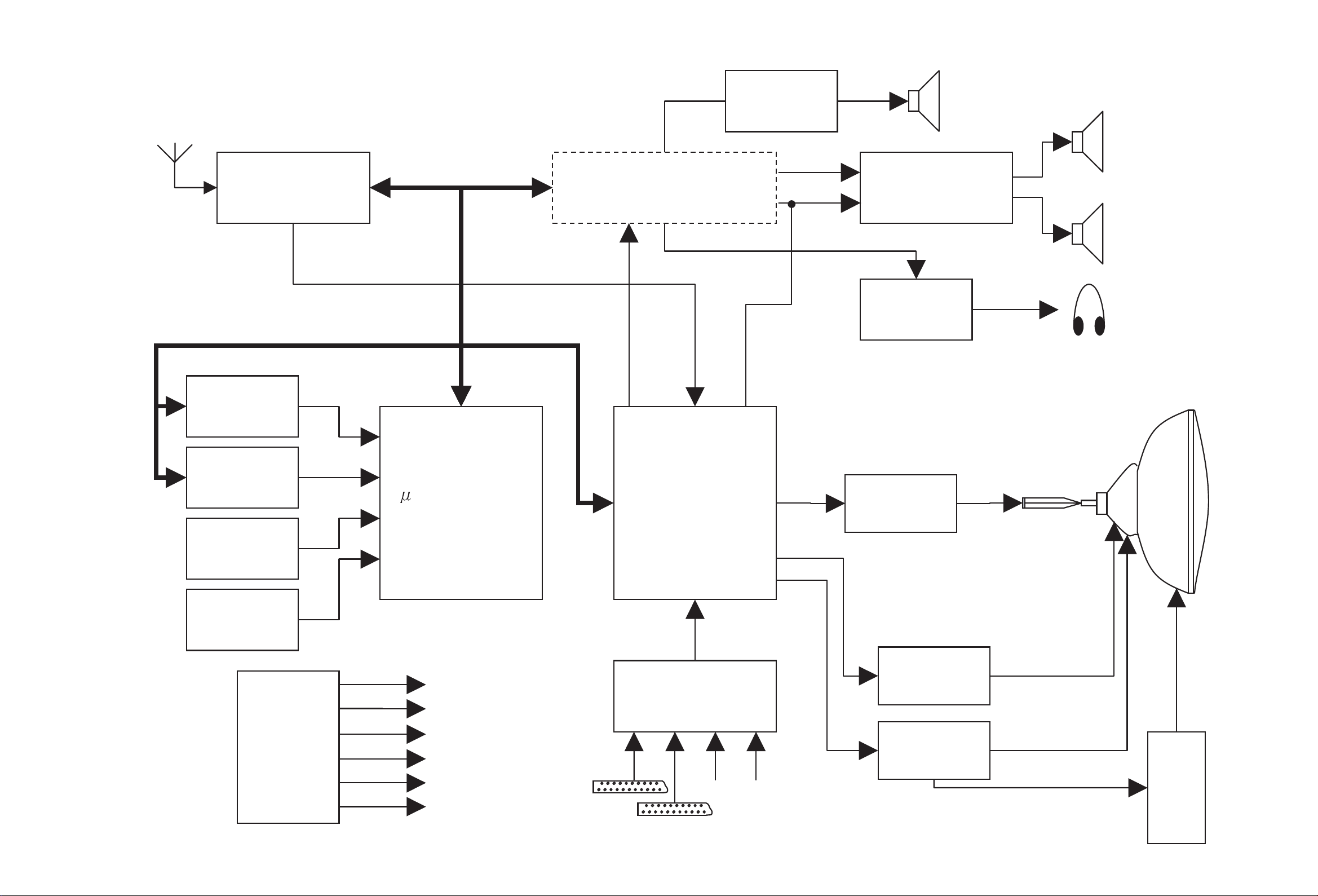
BLOCK DIAGRAM
AV-25BT6ENS
AV-25BT6ENB
AV-25BT6ENS
AV-25BT6ENB
PLL/VST TUNER
UV1315/16
SERVICE
CONNECTOR
I2 C
STEREO SOUND
MSP34X0D/G
VIRTUAL DOLBY
QSS
MSP 3411G
IF
SUB AMP
SUBW
TDA7261
L
L
AUDIO AMP
TDA7269A
R
R
HP AMP
TDA1308
MONO
CRT
EEPROM
KEYPAD
IR
SENSOR
SMPS
MC446
08
CONTROLLER
ST92195
+150 B+
+14V
-14V
+8V
+5V
+5V STBY
SCART1
VIDEO
PROCESSOR
STV2248C
VIDEO
SWITCHING
CIRCUITS
SVHS FAV/BAV
RGB AMP
TDA6108
VER AMP
STV9306
HOR D
BU2508
RIVE
VER. DEFL.
HOR. DEFL.
FBT
No.52056
SC
ART 2
2-3 2-4
No.52056
Page 5

CIRCUIT DIAGRAMS
MAIN PWB CIRCUIT DIAGRAM [1/6]
AV-25BT6ENS
AV-25BT6ENB
AV-25BT6ENS
AV-25BT6ENB
0V
4.9V
0V
4.9V
0V
3.9V
4.8V
1.6V
4.9V
0V
1.4V
0V
1.6V
4V
4.9V
1.9V
1.8V
4.9V
1.4V
1.4V
MAIN PWB (1/6)
VE-20101572
(AV-25BT6ENS, AV-25BT6ENB)
IC501 40
3.9V
4.9V
0V
0V
0V
0.2V
1.8V
4.9V
0.9V
4.5V
6
IC501 41
5
1.6V
1.5V
0V
4.9V
0.2V
0.2V
4.9V
4.5V
0V
0V
0V
0V
0V
0V
1.6V
1.6V
0V
3.6V
0.1V
1.6V
0.2V
1.6V
1.6V
4.9V
0.1V
2.8V
2.5V 5.5V
0V
3.9V 3.5V
4.9V 4.9V 0V
23.3V
0V
0V
4.9V
4.9V
4.2V
4.9V
4.6V
No.52056 No.52056
2-5
0V
0V
2-6
Page 6

MAIN PWB CIRCUIT DIAGRAM [2/6]
AV-25BT6ENS
AV-25BT6ENB
AV-25BT6ENS
AV-25BT6ENB
MAIN PWB (2/6)
VE-20101572
(AV-25BT6ENS, AV-25BT6ENB)
15.1V
14.9V
12.1V
0V
12.1V
0V
-15.6V
2.4V
2.4V
2.3V
3V
2.5V
2.4V
2.4V
0V 12.1V
15.3V
0V
-15.6V
0V 0V 0V
0V
2.2V
1.9V
0V
3.8V
4.4V
2.9V
2.3V
3.8V
1.1V
3V
0V
4.8V
4V
3.9V
4V
0.9V
0.8V
5.5V
5.7V
7.9V
4V
0V
3.9V
IC403 48
2
IC403 47
2.3V
6
7.8V
2.8V
2.2V
3.8V
7.9V
IC403 32
3.5
No.52056
IC403 31
4
IC403 30
4
2-7 2-8
3.5V
0.1V
3.1V
2.5V
1.6V
3.8V
2.4V
1.7V
2.4V
3.1V
0V
0V
4.1V
4.1V
0.1V
4.3V
2.5V
2.5V
2.5V
4.3V
No.52056
Page 7

MAIN PWB CIRCUIT DIAGRAM [3/6]
AV-25BT6ENS
AV-25BT6ENB
AV-25BT6ENS
AV-25BT6ENB
4.9V
4V
4.8V
3.3V
7.9V
2.2V
0.1V
7.9V
0V
0.1V
MAIN PWB (3/6)
VE-20101572
(AV-25BT6ENS, AV-25BT6ENB)
7.9V
0V
No.52056 No.52056
2-9 2-10
Page 8

MAIN PWB CIRCUIT DIAGRAM [4/6]
AV-25BT6ENS
AV-25BT6ENB
AV-25BT6ENS
AV-25BT6ENB
MAIN PWB
VE-20101572
IC601 2
3
(4/6)
(AV-25BT6ENS, AV-25BT6ENB)
IC601 5
30
Q601 B
2
-0.1V
IC601 6
2
193V
0V
1300
IC601 7
60
3.9V 3.4V
3.9V
3.3V
0V
5.5V
5.5V 26.3V
5.5V
1.4V
0V 12.6V
26.9V
1.2V
12.6V 3.1V
12.6V 4.3V
6.8V
7.4V
13.6V
11.8V
0V
0V
14.7V
No.52056
-0.1V
0V
TR601 4
300
TR601 5
250
TR601 6
120
TR601 8
25
2-11 2-12
TR601 9
65
No.52056
3.6V
5.8V
0V
Page 9

MAIN PWB CIRCUIT DIAGRAM [5/6]
AV-25BT6ENS
AV-25BT6ENB
AV-25BT6ENS
AV-25BT6ENB
12.2V
12.2V
9.4V
4.9V
4.9V
7.9V
0.1V
4.9V
1.1V
107.5V
2.5V
281V
0V
0V
0.6V
0V
12.5V
2.5V
MAIN PWB (5/6)
12.5V
4.9V
No.52056 No.52056
2-13
12.2V
11.1V
2.3V
0.1V
2-14
VE-20101572
(AV-25BT6ENS, AV-25BT6ENB)
Page 10

MAIN PWB CIRCUIT DIAGRAM [6/6]
AV-25BT6ENS
AV-25BT6ENB
AV-25BT6ENS
AV-25BT6ENB
1.4V
0V
0V
1.4V
0V
0V
1.4V1.4V
4.9V
0.1V
3.7V3.7V
0.1V
1.6V
0V
1.5V
0V3.7V3.7V
0V4.9V
0.1V
4.9V
0.1V
4.8V
4.2V
0V4.9V
4V3.2V
2.5V3.7V
2.4V
2.4V
3.7V3.7V
0V
3.7V3.7V
1.6V1.7V2.3V
3.6V
0V
6.8V
6.1V7.9V
2V2V4.8V0V
0V
3.7V
0.1V
3.7V
0.1V
0V
0.1V
3.7V
0.1V
3.7V
0.1V
No.52056
2-15
2-16
MAIN PWB (6/6)
VE-20101572
No.52056
(AV-25BT6ENS, AV-25BT6ENB)
Page 11

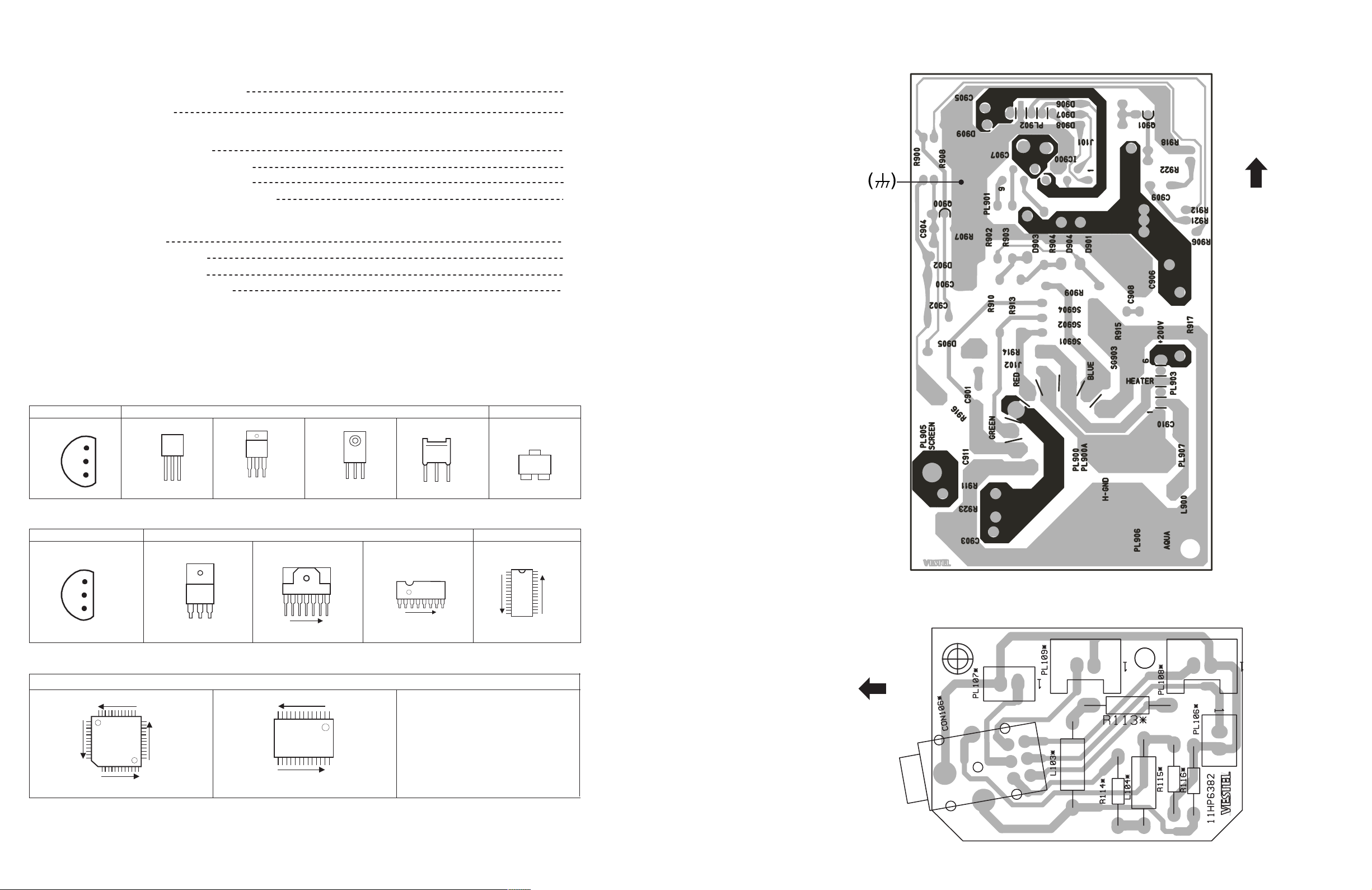
CRT SOCKET PWB CIRCUIT DIAGRAM
AV-25BT6ENS
AV-25BT6ENB
AV-25BT6ENS
AV-25BT6ENB
3.8V
0V
IC900 7
150 140
2.5V 2.5V
2.5V
IC900 8
0V
4.8V
201V
IC900 9
160
132V
145V
CRT SOCKET
PL902
133V
195V
-0.9V
CRT SOCKET PWB
VE-20094670
(AV-28BT8ENS, AV-28BT8ENB)
(AV-28BT8EPS, AV-28BT8EPB)
(AV-28BT8EES, AV-28BT8EEB)
No.52056 No.52056
2-17
2-18
Page 12

HEADPHONE PWB CIRCUIT DIAGRAM
FRONT CONTROL PWB
(AV-25BT6ENS, AV-25BT6ENB)
VE-20083646
HEADPHONE PWB
VE-20079493
(AV-25BT6ENS, AV-25BT6ENB)
AV-25BT6ENS
AV-25BT6ENB
AV-25BT6ENS
AV-25BT6ENB
FRONT CONTROL PWB CIRCUIT DIAGRAM
No.52056
2-19
2-20
No.52056
Page 13

PATTERN DIAGRAMS MAIN PWB PATTERN
FRONT
AV-25BT6ENS
AV-25BT6ENB
AV-25BT6ENS
AV-25BT6ENB
No.52056 No.52056
2-21
2-22
Page 14

VICTOR COMPANY OF JAPAN, LIMITED
HOME AV NETWORK BUSINESS UNIT. 12, 3-chome, Moriya-cho, Kanagawa-ku, Yokohama, Kanagawa-prefecture, 221-8528, Japan
VP 0207
DP6060
 Loading...