

Page 1
B
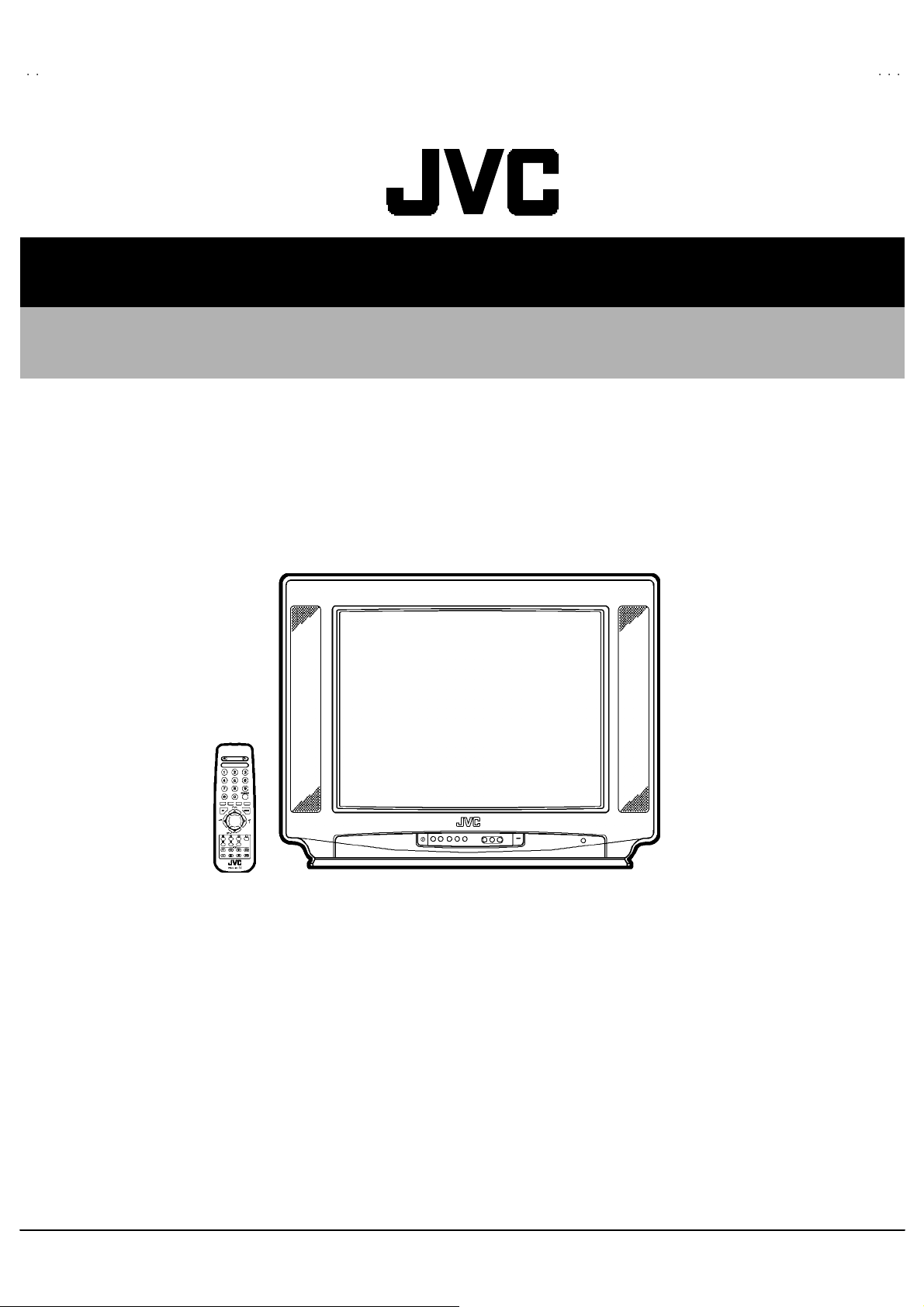
SERVICE MANUAL
COLOUR TELEVISION
AV25BT6ENS
AV25BT6ENB
AV-25BT6ENS
AV-25BT6EN
CONTENTS
! SPECIFICATIONS ・・・・・・・・・・・・・・・・・・・・・・・・・・・・・・・・
!
SAFETY PRECAUT IONS
!
FEATURES・・・・・・・・・・・・・・・・・・・・・・・・・・・・・・・・
! MAIN DIFFERENCE LIST ・・・・・・・・・・・・・・・・・・・・・・・・・・・・・・・・
!
SPECIFIC SERVICE INSTRUCTIONS
! SERVICE ADJUSTMENTS ・・・・・・・・・・・・・・・・・・・・・・・・・・・・・・・・
! PARTS LIST ・・・・・・・・・・・・・・・・・・・・・・・・・・・・・・・・
★
OPERATING INSTRUCTIONS
★
STAND ARD CIRCUIT DIAGRAM
1
・・・・・・・・・・・・・・・・・・・・・・・・・・・・・・・・・・・・・・・・・・・・・・・・・・・・・・・・・・・・・・・・
・・・・・・・・・・・・・・・・・・・・・・・・・・・・・・・・・・・・・・・・・・・・・・・・・・・・・・・・・・・・・・・・
・・・・・・・・・・・・・・・・・・・・・・・・・・・・・・・・・・・・・・・・・・・・・・・・・・・・・・・・・・・・・
・・・・・・・・・・・・・・・・・・・・・・・・・・・・・・・・・・・・・・・・・・・・・・・・・・・・・・・・・・・・・・・・
・・・・・・・・・・・・・・・・・・・・・・・・・・・・・・・・
・・・・・・・・・・・・・・・・・・・・・・・・・・・・・・・・・・・・・・・・・・・・・・・・・・・・・・・
・・・・・・・・・・・・・・・・・・・・・・・・・・・・・・・・・・・・・・・・・・・・・・・・・・・・・・・・・・・・・・・・
・・・・・・・・・・・・・・・・・・・・・・・・・・・・・・・・・・・
・・・・・・・・・・・・・・・・・・・・・・・・・・・・・・・・・・・・・・・・・・・・・・・・・・・・・・・・・・・・・・・・
・・・・・・・・・・・・・・・・・・・・・・・・・・・・・・・・・・・・・・・・・・・・・・・・・・・・・・・
・・・・・・・・・・・・・・・・・・・・・・・・・・・・・・・・・・・・・・・・・・・・・・・・・・・・・・・・・・・・・・・・
・・・・・・・・・・・・・・・・・・・・・・・・・・・・・・・・
・・・・・・・・・・・・・・・・・・・・・・・・・・・・・・・・・・・・・・・・・・・・・
・・・・・・・・・・・・・・・・・・・・・・・・・・・・・・・・・・・・・・・・・・・・・・・・・・・・・・・・・・・・・・・・
・・・・・・・・・・・・・・・・・・・・・・・・・・・・・・・・・・・・・・・・・・・・・・・・・・・・・
・・・・・・・・・・・・・・・・・・・・・・・・・・・・・・・・・・・・・・・・・・・・・・・・・・・・・・・・・・・・・・・・
・・・・・・・・・・・・・・・・・・・・・・・・・・・・・・・・・・・・・・・・・・・・・・・・・・・・・・・・・・・・・・・・
・・・・・・・・・・・・・・・・・・・・・・・・・・・・・・・・・・・・・・・・・・・・・・・・・・・・・・・・・・・・・・・・
・・・・・・・・・・・・・・・・・・・・・・・・・・・・・・・・
・・・・・・・・・・・・・・・・・・・・・・・・・・・・・・・・・・・・・・・・・・・・・・・・
・・・・・・・・・・・・・・・・・・・・・・・・・・・・・・・・・・・・・・・・・・・・・・・・・・・・・・・・・・・・・・・・
COPYRIGHT © 2002 VICTOR COMPANY OF JAPAN, LTD.
・・・・・・・・・・・・・・・・・・・・・・・・・・・・・ 2
・・・・・・・・・・・・・・・・・・・・・・・・・・・・・・・・・・・・・・・・・・・・・・・・・・・・・・・・・・
・・・・・・・・・・・・・・・・・・・・・・・・・・・・・・・・・・・・ 21
・・・・・・・・・・・・・・・・・・・・・・・・・・・・・・・・・・・・・・・・・・・・・・・・・・・・・・・・・・・・・・・・
・・・・・・・・・・・・・・・・・・・・・・・
・・・・・・・・・・・・・・・・・・・・・・・・・・・・・・・・・・・・・・・・・・・・・・
・・・ 5
・・・・・・
・・・・・・・・・・・・・・・・・・・・・・・ 5
・・・・・・・・・・・・・・・・・・・・・・・・・・・・・・・・・・・・・・・・・・・・・・
・・・・・・・・・・・・・
・・・・・・・・・・・・・・・・・・・・・・・・・・
・・・・・・・・・・・・・・・・・・・・・ 10
・・・・・・・・・・・・・・・・・・・・・・・・・・・・・・・・・・・・・・・・・・
・・・・・・・・・・・・・・・・
・・・・・・・・・・・・・・・・・・・・・・・・・・・・・・・・
2- 1
4
6
No.520 56
Jul. 200 2
Page 2
A
V-25BT6ENS
A
V-25BT6ENB
SPECIFICATIONS
Content
ITEM
Dimensions ( WxHxD) 69 cm x 5 4 cm x 47 cm
Weight 27 kg
TV RF System B/G
Colour Syst em
Teletext System Fast ext / Toptext
Stere o Sy st em German + NICAM
Tuning System Fr equenc y Synt hes iz er T un in g S ystem
Numb er Of CH me mory pos ition 10 0 ch
Receiving Frequency
Intermediate Fr equency
Colour Sub Carrier Frequency PAL (4.43MHz), SECAM (4.43MHz), NTSC (3.58MHz/4.43MHz)
Aerial Input Terminal 75 Ohm U n bala nced
Power Input AC 2 20V ~ 240V, 50H z
Power Consumption 135W(Max.) 1.8W (stand by)
Pictur e Tube Visi bl e size : 59cm ( M eas u r ed d iago na lly)
Hi gh Vo l t ag e 30 .45kV
Speake r 5.7 X 16 cm Oval type X 2
Au dio Output 10W + 10W
Input
Output
Remote Control Unit VE -3 00 17763 (R M-C11 00) , Batte ry s ize :AA /R 06 dry b att er y x 2
TV Mode PA L
Video Mode PAL / NTSC 3 .58 / NTSC 4 .43
VHF (VL) 46 .25 MH Z ~ 1 68. 25MH z
VHF (VH) 17 5.2 5MH z ~ 46 3.2 5MHz
UHF 47 1.2 5MH z ~ 863.2 5MH z
CATV S01-S 4 1 & S7 5- S79
VIF Carrier 38 .9 MHz
32.4 MHz (6.5 MHz)
SIF Carrier
Vide o 1Vp-p, 75 Ohm
S/V ideo
Au di o (L/R)50 0 mV r ms, High I mp edance
Vide o 1 Vp -p, 75 Ohm
Au di o (L/R)50 0 mV r ms, L ow Imped ance
Rear Sid e
Front Side AV 3 ( Vid eo/A ud i o)
Front Side Hea dph on e jac k (S ter e o mi ni jack 3.5∅)
Rear Sid e
32.9 MHz (6.0 MHz)
33.4 MHz (5.5 MHz)
Y: 1Vp -p Posi ti v e
C: 0. 286Vp -p
AV 1 ( Vi d eo/Aud i o/R GB)
AV 2 (Vid eo/A udio/S-VHS)Input Terminal
AV1 (V ideo/Au dio)Output Terminal
AV2 ( V ideo /Au dio) ( S electe d T V, AV1 o r AV3 )
AV-2 5BT 6EN S (S ilver)
AV -2 5BT 6EN B (Bl a ck )
De sign & speci f icatio ns ar e su bje ct to cha ng e wi thout no t ice.
2
No.52056
Page 3
A
V-25BT6ENS
A
V-25BT6ENB
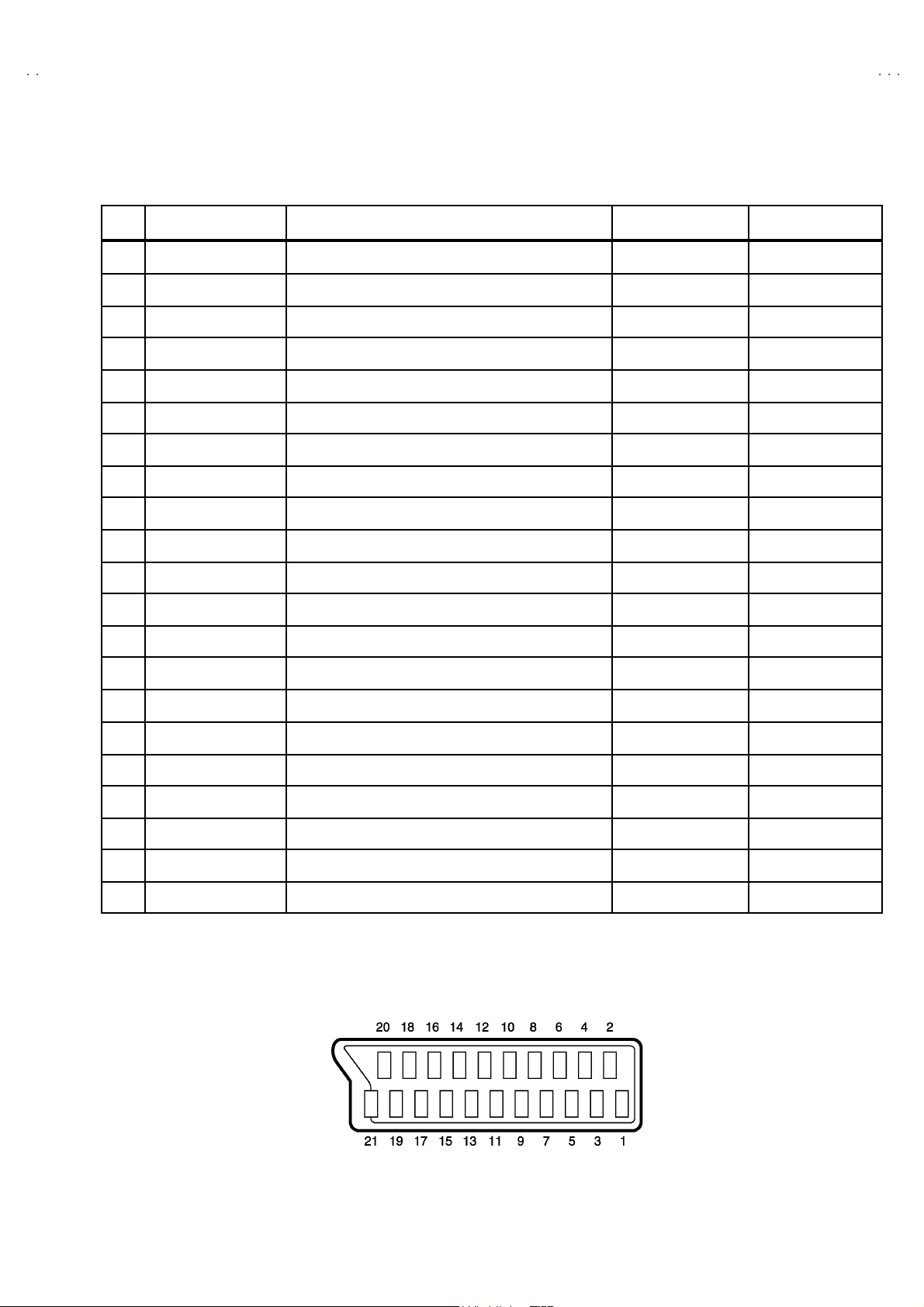
■■■■21-pin Euro connector (SCART socket) : AV1 / AV 2
(P-P= Peak to Peak, S-W= Sync tip to white peak, B-W= Blanking to white peak)
Pin
Signal Designation Matching Value AV-1 AV-2
No .
1 AUDIO R o utput 50 0m Vr ms(Nomina l) ,L ow impe dan ce
2 AUDIO R input 500mVrms(Nominal),High impedanc e ○○
3 AUDIO L outp ut 50 0m Vr ms(Nomina l),L ow i m pe dance
4 AUDIO G ND
5 GND (B) ○○
○
(TV OUT)
○
(TV OUT)
○○
○
(TV/LINE OUT)
○
(TV/LINE OUT)
6 AUDIO L input 500mVrms(Nominal), High impedance
B-W
7B input
FUNCTON SW
8
(SLOW SW)
9 GND (G)
10 - NC -
11 G in put
12
- NC -
13 GND (R)
14 GND (YS) ○ NC
15 R / C input
16 Ys i n put L ow : 0 – 0.4, Hig h : 1 - 3 V, 75 Ω○NC
17 GND(VIDEO output)
18 GND(VIDEO input) ○○
19 VID EO outpu t
20 VIDEO / Y inp ut 1V
70 0m V
Low : 0-3V, High : 8-12V, High impedance
70 0m V
R : 700mV
C : 300mV
1V
, 75Ω○
B-W
, 75Ω○
B-W
, 75Ω
P-P
, 75Ω
S-W
(Negative going sync), 75Ω
S-W
(Negative going sync), 75Ω○○
○○
NC
○
○○
○○
○
(R/C)
○○
○
(TV)
NC
NC
○
(only C )
○
(TV/LINE OUT)
21 COMMON G ND
○○
[Pin assignment]
No.52056
3
Page 4

A
V-25BT6ENS
A
V-25BT6ENB
SAFETY PRECAUTIONS
1. The design of th is prod uct con ta in s sp eci al har d ware , many
circuit s and components specially for saf ety purposes. For
con tinu ed pr ot ecti on , n o chan g es sh ould b e ma de to the o rig i nal
d esign un less a uth or ized in writi n g by th e manu fac t urer .
Replacem ent p arts m ust b e i d entic al to thos e u sed in th e or i gi n al
ci rcu its. Se r v ic e s h ou ld be pe rf or me d b y qua li fi e d per so nn el
on ly.
2. Alte r ation s of the desi g n or circui tr y of t he prod ucts s h oul d not be
made. Any design alterations or additions will void the
manu fac t urer 's warra nt y and will f urth er r el i eve t he ma nufac tu rer
of r esp onsib ili ty for per s o na l injury or pr operty d am ag e res ul t ing
th erefr om.
3. Man y e l ectr ical an d mech ani c a l p ar ts i n th e pr od ucts ha v e
special safety-related chara cteristics. T hese characteristics are
oft en no t e vi den t f r om v i sua l insp ecti on nor ca n t he pro tect io n
aff orde d by th em nece ssarily be ob tain ed b y u s in g r ep l ac em en t
com po nents rated for hig he r vo l tag e, watt age, etc . R ep lac em en t
p arts whic h have th ese sp ecial s afet y ch ar act erist ics ar e
ide ntified in the parts list of Ser vic e manua l. El ectric al
components having such features are ide ntified by shading
on the sche mat ic s and b y (!!!! ) on the parts list in Service
manual. The us e of a sub sti tu te r ep lac em en t which do es n ot
h ave th e sam e s af ety c h ar ac t erist ics as t he reco mmen ded
replac ement par t sh ow n i n th e parts list of Ser v i ce man ual m ay
cause shock, fire, or other hazards.
4. Don't shor t between the LIVE s ide ground and ISOLATED
(NE UTRAL) s ide ground or EARTH side ground when
repairing.
Some model's power circuit is partly different in the GND. The
diff er enc e of the GND is sh ow n b y th e LI VE si de G ND, th e
ISO LATE D(N EU TR AL) sid e GND and EARTH side GND. Don' t
sh ort b etw ee n the L IVE side GND a nd IS OLATE D(NEUTR AL)
si de GN D or EARTH si de GND an d ne v er meas ure with a
measu rin g app aratu s (osc illosc ope et c.) th e LIV E sid e GND an d
ISOLATED(NEUTRAL) side GND or EARTH side GND at the
same time.
If above not e will not be kept, a fuse or any parts will be broken.
5. If any repair has been made to the chassis, it is recommended
th at t he B1 set ting shou l d b e c h ec ked or adju ste d ( Se e
ADJUSTM ENT OF B 1 POW E R SUPPLY).
6. The hi gh vol ta ge app lie d t o th e pi ctu r e tu be mu s t c on form wit h
th at sp ecifi ed i n S ervi ce man ual . E xc essi ve h i gh volt ag e c a n
cau se an i ncr e ase i n X- R ay em iss i on , arci ng an d possi b le
component damage, therefore operation under excessive high
voltage conditions should be kept to a minimum, or should be
preve nt ed. If s ever e arc ing occur s, r emov e t he AC power
immed iate l y and de ter m i ne th e ca us e b y vi sua l insp ec t ion
(incor r ec t in stal lat i on, cr ac ke d or melte d hi gh v o lt age harn ess,
p oor so ld er ing, et c.) . T o m ai nt ain the prope r mi n imu m le vel of
sof t X- R ay em iss i on, c omp on en ts i n th e hi gh voltag e c i r cuitr y
incl ud i ng t he pict ure tu be must b e t he e xact r ep l ac em e nts or
alte rn at ives ap pr ove d b y th e manuf ac t urer of th e c omplet e
prod uct.
7. Do not c hec k hi gh volt ag e by dr aw i ng an arc. Use a hi gh volt age
meter or a hig h v oltag e pr ob e wit h a V TVM . Discha rg e th e
picture tube before attempting meter connection, by connecting
a cl i p le ad to th e gr ou nd f rame a nd c onn ecti n g th e oth er end of
the lead through a 10kΩ 2W resi s to r to the anod e butt on .
8. When se r vic e is r equ ire d, ob serve th e or i gina l lea d dr ess. E x tr a
prec aut i on sh ou ld b e given t o assur e cor r ect l ea d dress in th e
high vol tag e circui t a rea. W her e a s hor t c i r cuit h as occ u rr e d,
th ose co mpon ent s tha t indica te evide nce of ove r hea ting should
b e r e place d. A lways u s e th e manuf act ur er 's rep lacem ent
components.
9. Isolation Check
(Safety for Electrical Shock Hazard)
Af ter r e- ass embl in g th e p r odu ct, always per f orm an i solat io n
ch eck on the expo s ed me tal p ar ts of t he cabin et ( a nte nn a
ter m i na ls, vid eo /au dio i npu t and outpu t t ermi n al s, C on trol kn obs,
metal cabinet, screwheads, earphone jack, control shafts, etc.)
to be su re th e p r odu ct is s af e t o o pe rate with ou t d an ger of
elect rical shoc k.
(1) Dielectric Strength Test
The iso lation be tw een the AC pr im a ry ci rcu it an d al l me tal p arts
exp osed t o the us er, p ar ticular ly an y e xpos ed met al p art having a
retu rn p ath to t he c hass is sho uld withs tan d a vol t age of 3000 V
AC (r.m. s.) for a period of one second.
(. . . . W it hstan d a v o lt age of 110 0V A C (r .m. s.) t o an ap pli anc e
rate d up to 12 0V , an d 3 00 0V AC ( r.m. s.) to an ap pl i an c e r at ed
200V or more, for a period of one second.)
This meth od of test r equi res a test equipment n ot g enerall y fou nd
in t he serv ic e trad e.
(2) Leakage Current Check
Plug th e AC l in e c ord d irect ly into the A C ou tlet ( d o not use a lin e
isol ati o n transf orm er du r ing this ch eck.). U sin g a " Lea kag e
Current T este r", me as ur e th e l ea k ag e cu rr e nt f rom eac h ex p os ed
metal p ar t of the cabine t, p art icu lar ly any e x pos ed me tal p art
h aving a re turn pa th to the ch assis , to a kn own go od ea rt h
grou nd (w a ter pip e, e tc.). An y l eaka ge c ur r en t must n ot e xceed
0.5mA AC (r.m.s.).
Howev e r, in trop ic al ar ea , th is mu st no t ex ce ed 0.2 mA AC
(r.m.s.).
"""" Alte rn at e Che ck M et hod
Plug th e AC l in e c ord d irect ly into the A C ou tlet ( d o not use a lin e
isol ati o n tran sfor m er dur i ng this c he c k.). Use an AC vo lt meter
h aving 1 00 0 oh ms pe r vol t or mor e s ens it i vity i n th e fo llowi ng
mann er . C on nec t a 1 50 0Ω 10W res ist or par a lle le d b y a 0 .1 5µF
AC-type c apa cit or bet ween an expo sed met al pa rt and a kno wn
g ood e ar th gr o und (water pi pe , etc.) . M eas ur e th e A C volt ag e
acr os s th e res ist or wi th th e AC vo l tm eter. Move th e r es i stor
con nec tion to e ach exp ose d me tal part, p art i cularly any exp osed
metal p ar t havi n g a r etu rn pat h to the ch assis, and m easu r e th e
AC vol tag e ac ros s the res ist or. No w , re v er se th e pl u g in th e AC
ou tl et and re pe at eac h mea suremen t. An y vol t ag e me asu re d
must no t e xc eed 0 .7 5V AC (r.m. s.) . This c orre spo nds to 0 .5mA
AC (r.m. s.).
Howeve r, in tropica l area, this must n ot exce ed 0 .3V AC ( r .m.s.).
This corresponds to 0.2mA AC (r.m.s.).
AC VOLT MET ER
(HAVING 1000 Ω /V,
OR MOR E SENSIT IVITY)
0.15μF AC -T YPE
PLACE THIS PROBE
1500 Ω 10W
GOOD EARTH GROUND
ON E A C H EX PO SE D
ME T AL PA RT
4
No.52056
Page 5
A
A
FEATURES
V-25BT6ENS
V-25BT6ENB
1. It is a remote controlled color television.
2. 10 0 prog r am s fr om VH F, UHF b an ds or cab l e cha nn els can be
pres et.
3. It c an tun e cable cha nn el s.
4. Cont ro l lin g th e TV i s ver y eas y by i ts m en u dr i ve n s yst em .
5. It h as two Eu r oc on n ector s ockets for exte rnal de vice (suc h as
vi de o reco rder , vid eo games , a udi o set, etc.)
6. F r ont AV Inp ut avai l a ble.
7. St ereo s ound s ystem s ( Ger m an + Nic am ) ar e a vailab le.
8. Full fu ncti o n Tele text (Fast ext, Topte xt).
9. It i s possi b le to connec t head ph on e.
10. Direct channel access.
11 . APS (Aut omat ic P r ogr am m i ng Syste m).
12 . All pr og r ams ca n b e nam ed .
13 . Forward o r bac kward au to ma ti c tu ning .
14 . Au tom at ic sou nd mu te when no tran smiss i on .
15 . 5 minu tes aft er the br o adc asti ng ( c l osed own) , the TV s witc h es
16. Child Lock.
MAIN DIFFERENCE LIST
!!!!
Parts Name
!
POW E R BUTTO N VE -2 00 43532 VE -2 00 00903
MODEL No.
AV -2 5 B T 6 EN S
(Silv er)
itsel f aut omati ca lly t o st and- by mod e.
AV -2 5 B T 6 EN B
(Bl ack )
! FRON T CABIN ET VE -200 46446 VE -2 00041 31
!
FU NCTION B UTTO N VE -2 00 43545 VE -200 03730
! REAR C OVE R VE -2 00 92523 VE -201 01575
CARTON BOX VE -500 28494 VE -5 00 28507
! RAT IN G L ABE L VE -2 01 02134 VE -201 02164
No.52056
5
Page 6
A
V-25BT6ENS
A
S
C
V-25BT6ENB
SPECIFIC SERVICE INSTRUCTIONS
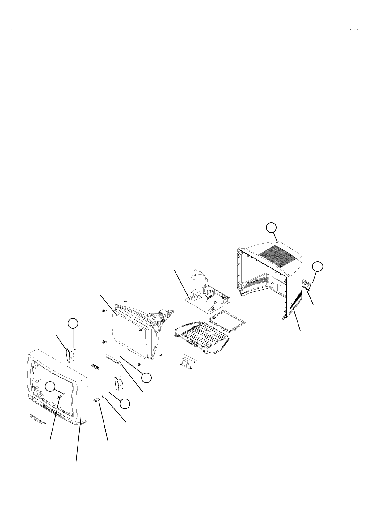
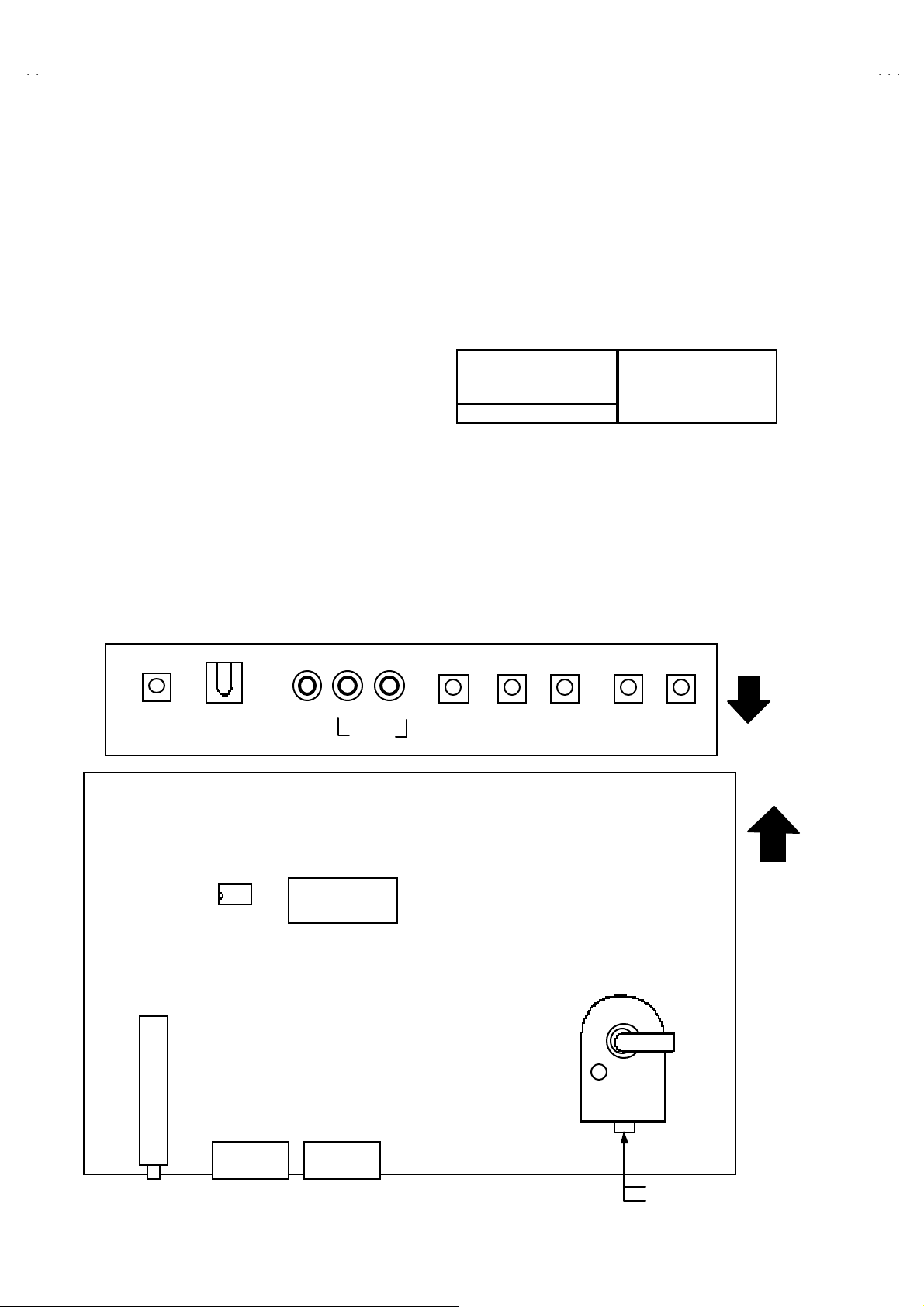
DISASSEMBLY PROCEDURE
REMOVING THE REAR COVER
1. Rem ove th e 8 screws marked A.
2. Rem ove th e 2 screws marked B.
3. W ithdr a w t he r ear c o ver to wa rd y ou .
REMOVING THE MAIN PWB ASS’Y
" Af ter removing the rear cover .
1. Yo u c an pull o ut the MA IN PW B ASS’Y.
REMOVING THE HEADPHONE PWB ASS’Y
" Af ter removing the rear cover.
1. Rem ove th e 1 screw marked C.
2. Remove th e H EA DP HO NE PWB AS S’Y & BRACK ET.
REMOVING THE SPEAKER
"
1. R em ove th e 4 screws marke d D.
2. Remove the SP EAK ER.
REMOVING THE FRONT CONT ROL PWB
" After removing the rear cover.
"
1. R em ove the 4 screws marked E a nd r em ov e th e FR ONT
REMOVING THE POWER SW
"
" Rem ove the M AIN PW B AS S’Y.
"
MAIN PWB
After removing the rear cover.
Remove th e M AIN PW B AS S’Y.
CONTROL PWB.
After removing the rear cover .
Remove the 2 screws marked F, and remove th e POW ER SW.
A
B
PEAKER
F
POWER S W
RT
AV
TERMINAL
BOARD
D
REAR COVER
E
FRONT CONT ROL PWB
C
BRACKET
HEADPHONE
PWB
FRONT CABINET
6
No.52056
Page 7
A
A
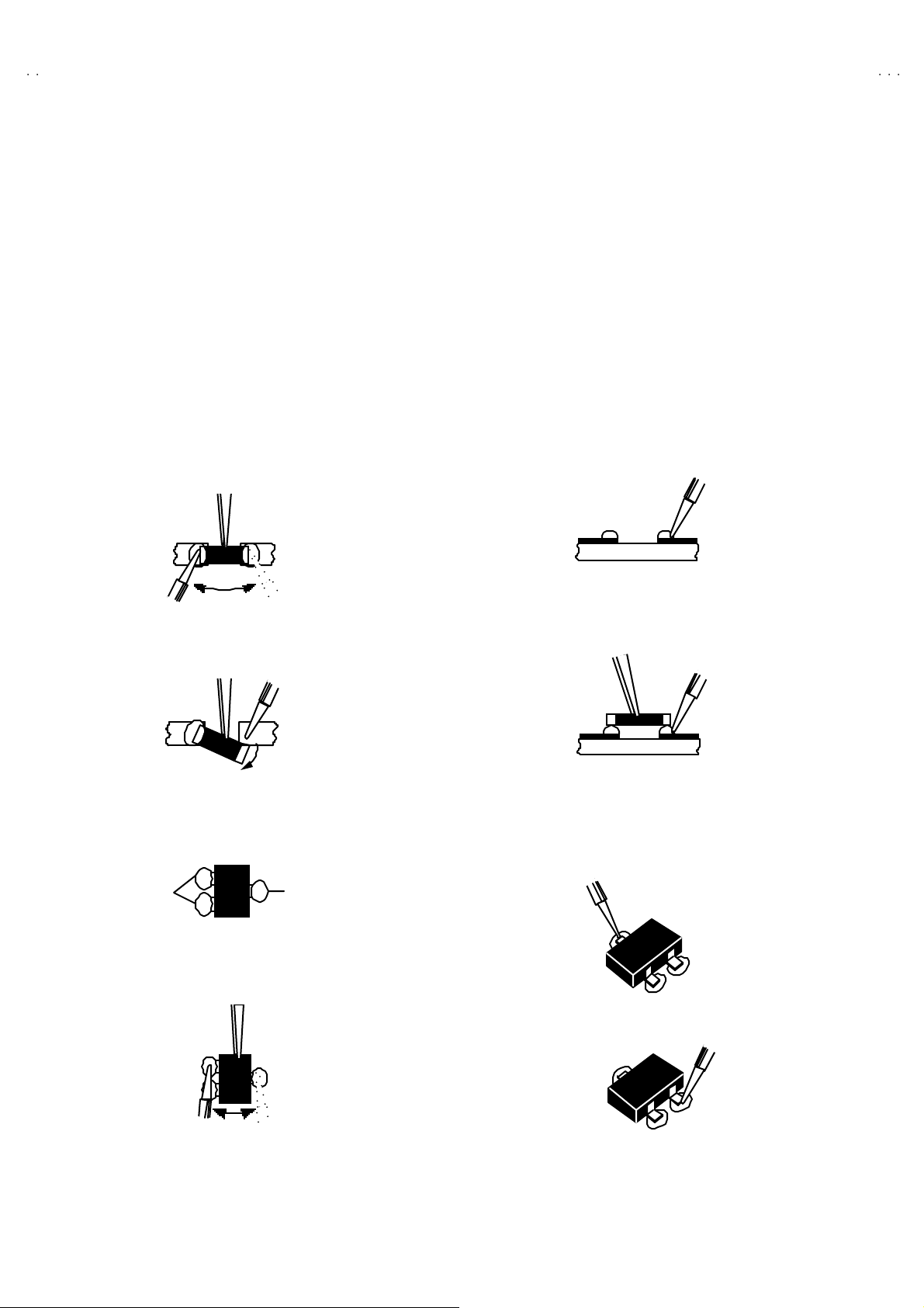
REPLACEMENT OF CHIP COMPONENT
! CAUTIONS
1. Avoid heating for more than 3 seconds.
2. Do n ot ru b the elect ro des an d the r esist p arts of the p att ern.
3. W hen r em oving a chip par t, mel t th e s older ad equately.
4. Do n ot reuse a ch ip p ar t afte r re mo v ing it .
! SOLDERING IRON
1. Use a hig h i ns ulatio n s ol der i ng i r on with a thi n poin ted e nd of it.
2. A 3 0 w s older i ng iron is r ec ommend ed for easily r em oving p ar ts.
!
REPLACEMENT STEPS
1. How to remove Chip parts
# Resi st ors, ca pa cit o rs , etc .
(1) As s ho wn in th e figure, pus h the pa rt with tw ee zer s a nd
alte rn at ely melt the s ol de r at eac h end.
V-25BT6ENS
V-25BT6ENB
2. How to install Chip parts
# Resi st ors, ca pa cit o rs , etc .
(1) Apply sold er to the patt ern as ind ic ated in the fig ure.
(2) Sh if t w i th tw eeze rs and r em ove th e c h i p p art.
#
Trans ist ors, diodes , varia bl e r esistor s, etc.
(1) Ap pl y e xt ra so ld er to eac h le ad .
SOLDE R
(2) As s ho wn in th e figure, pus h the pa rt with tw ee zer s a nd
alte rn at ely m elt the sold er at e ach l e ad . Shift and r em ove
the chip p art.
SOLDE R
(2) Gr asp th e ch i p p art wit h t weez ers and p l ace it on th e
sol d er . Th en h eat and me lt the so lder at b oth e nds of the
chip part.
#
Trans ist ors, diodes , varia bl e r esistor s, etc.
(1) Apply sold er to the patt ern as ind ic ated in the fig ure.
(2) Gr asp th e ch i p p art wit h t weez ers and p l ace it on th e
solder.
(3) First s older lead A as indicated i n t he figu re.
A
B
C
(4) The n so ld er l e ads B and C.
A
B
Note : After removing the part, remove remaining solder from
the p atte rn.
No. 52056
C
7
Page 8
A
V-25BT6ENS
A
VALUE
VALUE
ITEM
MENU
MU T I NG
INFORMATION
COLOUR k
V-25BT6ENB
MEMORY IC REPLACEMENT
1. Memory IC
This model use a memory IC.
Thi s me mo r y I C st or es d ata for pr op er op er ati o n of the vid eo
an d d ef lecti on c ircu it s.
When replacing, be s ure to use an IC containing this (initial
valu e) data.
2. Memory IC rep lacemen t procedure
(1) Power off
Switch of f t he p ow er an d dis con nec t th e power co rd from
the wall outlet.
(2) Replace the memory IC
Init ial value m ust be entered into the n ew IC .
(3) Power on
Connect th e pow er c or d t o the wa ll o utlet an d s witc h on t he
power.
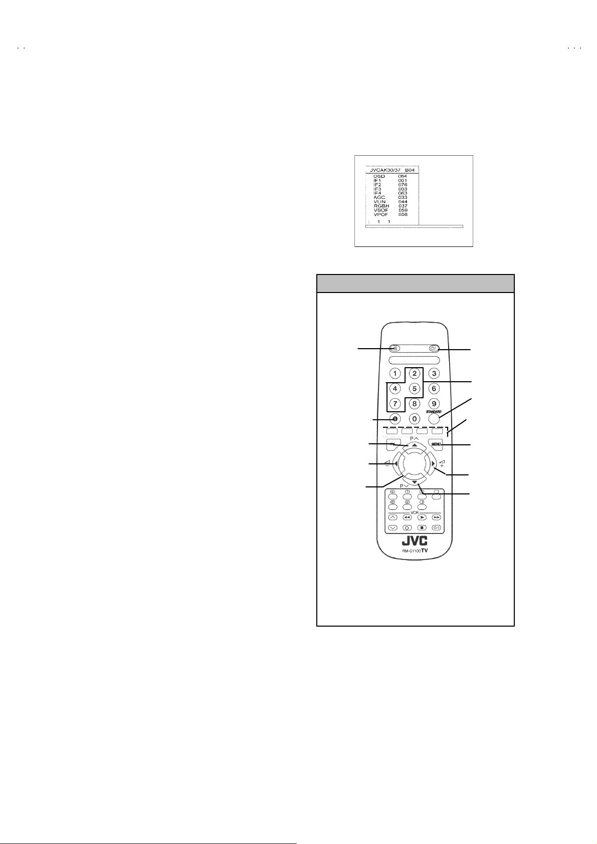
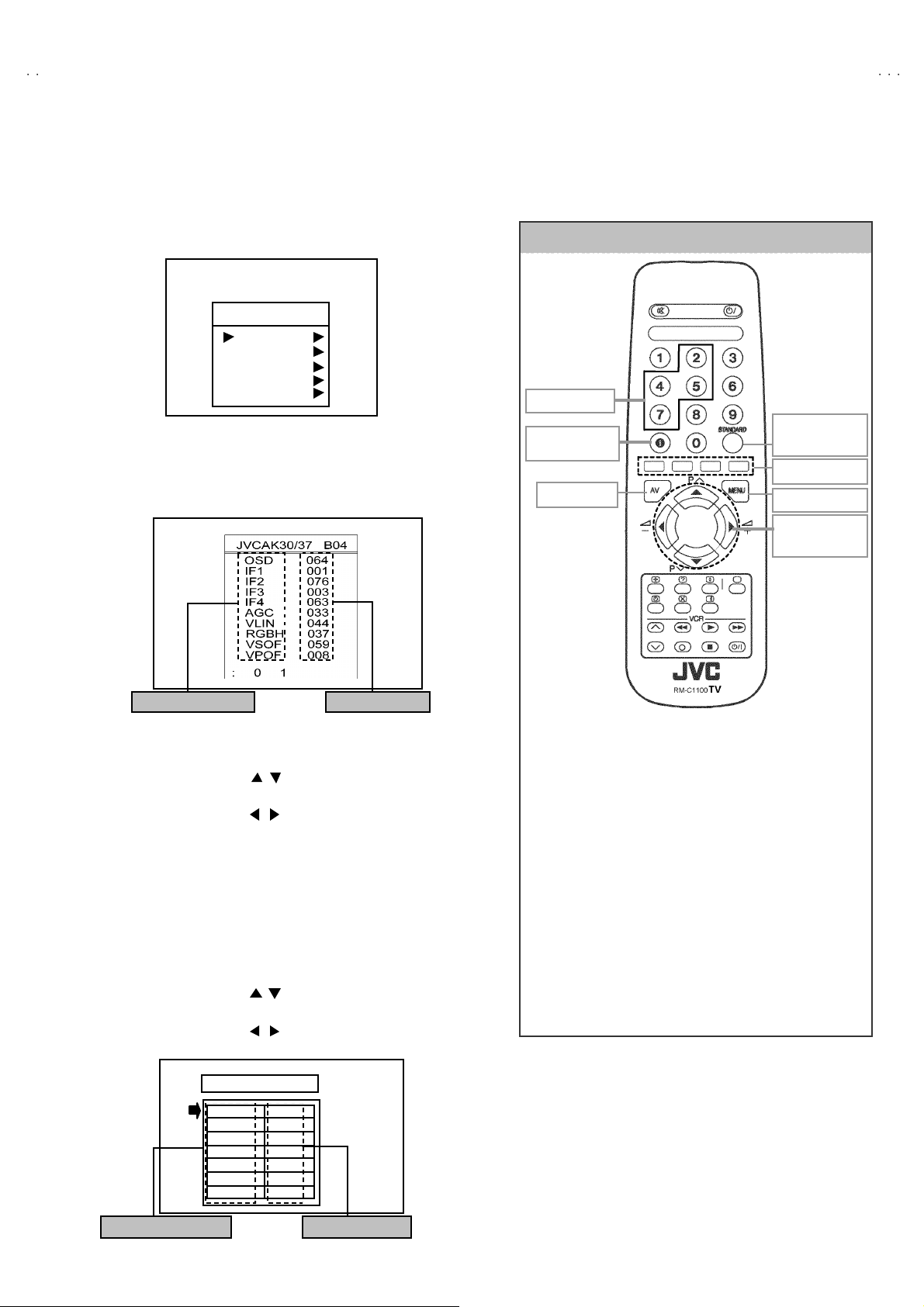
SE RVICE MENU
Fig.1
SERVICE MENU SELECT KEY
(4) SERVICE MENU setting
1) Pr ess MENU key and, while the displayed MENU
screen, press 4, 7, 2, 5 key on th e rem ote co ntrol uni t or
press MUTING key and INFORMATION key at the
simult aneously.
2) The SER V ICE M ENU sc r ee n of F i g.1 is d isp l ay ed .
3) Ve rif y what to s et i n the SER V ICE M EN U , and set
what ever is nec e s sary (Fig.1 ). Ref er to th e SE RVICE
ADJU STM ENT for settin g.
4) Press the STANDARD key to exit SERVICE MENU.
(5) Rec eiv e channel setting
Refe r to the OPERATIN G I N STRUCTIO NS ( USER ’S
GUID E) a nd set th e rece ive ch an nel s (Chan n els Pr eset ) as
described.
(6) User se tt ing s
Check th e us er s ett ing it ems ac c ordi ng to aft er pa ge .
Wher e th ese d o not a gr ee, r efer to t he OPE RAT ING
INSTRUCTIONS (USER’ S GUIDE) and set th e items as
described.
ITEM
SELECT(▲)
SELECT(-)
FUNCTION
POWER
NUMBER
STANDARD
ey
SELECT(+)
SELECT(▼)
Fig.2
8
No. 52056
Page 9
A
A
SETTING OF THE LAST MEMORY FOR SHIPMENT
■■■■ USER SETTING VAL UES
Setting Item Setting Value Setting Item Setting Value
SOUND MENU FEATURE MENU
BA LANCE CEN TER SL EEP TIMER OFF
BA SS
↑
CHILD LO CK OFF
V-25BT6ENS
V-25BT6ENB
TR EBL E
MODE STEREO AV-2 OUTPUT TV
EFFECT OFF
PICTURE MENU INSTALL
BRIGHTNESS PROGRAMME
CONTRAST BAND
COLOUR CHANNEL
SHAR PNES S SE ARCH
HUE (only NTSC)
PICTURE MODE AUTO STO RE
■■■■
SETTING APS BIT IN SERVICE MENU
1) En ter s er vic e me nu i n TV m ode by pr essi ng “IN FOR MA T ION” a nd “ M UTI NG” ke ys s i mu ltan eously. S er vic e M en u will ap pea r.
2) Se le c t T X1 (TEL ET EXT OPT IO N) b y pr essi n g Up /D ow n keys o n r em ot e c ontr o l un it.
3) Press the 7 key on remote control unit to set APS bit. (After this, bit 7 of TX1 will be “1”)
4) Press STANDARD key on remote control unit to exit service mode.
NOTE : DO NOT TURN OFF THE TV BY USING POWER BUTTON O N THE FRO NT PANEL.
Thes e ad j us t a re aut om ati ca lly
restore d when AP S b it in Se rvice
menu i s set .
The proc edure f or s e tti ng AP S
bit is describe d bellow.
↑
LANG UAGE ENGLISH
Refe r to t he INSTRUCTI ON
BOO K
FINE TUNING
No. 52056
9
Page 10
A
V-25BT6ENS
A
V-25BT6ENB
SERVICE ADJUSTMENTS
ADJUSTMENT PREPARATION:
1. You ca n ma ke t he ne ce ssa ry ad ju st me nts for t h is un it wit h
either the Remote Control Unit or With the adjustment tools
and parts as given below.
2. Adjustment with the Remote Control Unit i s made on the
basis of the initial setting va lues, however, the new setting
values which set the screen to its opti mum condition may
differ f rom the init ia l s ettings.
3. M ake sure t hat AC p ower is tu r ned on c orrec tly.
4. T ur n on the power for set an d test eq uip me nt bef or e use , and
start t he ad justmen t p roced ur es aft er w ai ti ng at least 30 minut es.
5. U nl ess o the r wise s pec if i ed, prep are t he most s u it able recep tion
or inp ut sign al for adjust ment.
6. Nev er tou ch any ad j ustm en t p ar ts wh ic h ar e n ot sp eci fied i n the
list for t his adjustment - variable resistors, transformers,
condensers, etc.
7. Pr esetti ng before ad j ustm en t.
Unl es s ot her w i se spec if i ed i n t he adjustme nt i nstr uct i ons , p r ese t
th e f ollo w ing f uncti ons with th e re mo te c ont ro l un it :
BRIGHT NES S
CONTRAST
COLOUR
SHAR PNES S
CENTER
ADJUSTMENT EQUIPMENT
1. DC voltmeter (or digital voltmeter)
2. Si gn al g ener at or (P attern g en erat or) [PAL/SECAM/NTSC]
3. Remote control unit
MAIN PARTS LOCATIONS
LE D
REMO CON
RECEIVER
IC50 2
ME MO RY I C
VIDEO R L
AUDIO.
IC50 1
MI CO M
ADJUSTMENT ITEM
!
SCR EEN A DJUST MENT
! OSD HORIZONTAL POSITION ADJ USTMENT
!
IF ADJU STMENT
! AGC AUTO MATI CALLY A DJUSTM EN T
!
DEFLECTION CI RCUIT ADJUSTMENT
! GEO MET RY ME NU ADJUSTME NT
!
WHITE BALANCE ADJUSTMENT
ME NU
(+)
(+) (-)
(+)(+)
PROG
/Ch.
(-)
(-)(-)
(+)
(+) (-)
(+)(+)
VOL
(-)
(-)(-)
TOP
FRONT
FBT
SCAR T
jack
TUNER
AV -1 AV -2
10
SCAR T
jack
UPPER : FOCUS VR
LOWE R : SCREEN VR
No. 52056
Page 11
A
A
BASIC OPERATION SERVICE MENU
■■■■ HOW TO ENTER THE SERVICE MENU
1) Pr ess the MENU key.
2) ME NU s c reen of fig.1 will b e d ispla ye d
MENU SCRE EN
MENU
SOUND
PICTURE
FEATURE
INSTALL
PROGRAM
V-25BT6ENS
V-25BT6ENB
REMOTE CONTROL UNI T key NAME
NUMBER key
Fig.1
3) W hil e the ME NU scr ee n is disp lay ed , p r ess th e 4,7 ,2, 5 k e y or
INFORMATION key and MUTING key simultaneously.
4) The SERVICE MENU screen of (Fig.2) will be displayed.
SE RVICE MENU
ADJUSTMENT ITEM SETTING VALUE
Fig.2
■ SELECTION OF ADJUSTMENT ITEMS
1) Enter th e SER VIC E ME NU
2) Press the FUNCTION / key and select the ADJUSTMENT
ITEM.
3) Pr ess the FUNCTION / ke y and s et t he SETTI NG VALUE.
■ HOW TO EXIT SERVICE MODE
1) Pr ess the STANDARD Key on REMOTE CO NTROL UNIT.
■ HOW TO ENTER THE GEOMETRY MENU
"
Thi s m o del is buil t- i n GEO ME T R Y M EN U f or ge omet ry
adjustment.
1) Enter th e SER VIC E ME NU
2) Press the GREEN key, geometry menu appears (Fig. 3).
3) Press the FUNCTION / key and select the ADJUSTMENT
ITEM.
4) Pr ess the FUNCTION / ke y and s et t he SETTI NG VALUE.
GEOME TRY MEN U
INFORMATION
key
AV key
" FUNC TI ON OF COL O UR k ey
RED key :
It switch es th e AV L to ON o r OF F mode on servic e
menu . AV L wo rd i s visible o n s er vice m en u when
AV L is o n.
GREE N k ey :
It s witch es t o GE OM ETR Y adjust menu. G eomet ry
of th e p ict ure i s a dj ust ed in th is m enu.
YELLOW key :
It s witch es t o VE RT ICAL SC AN DISA BLE mode.
It i s us eful t o adj ust scr een volt age.
BL UE ke y :
It i s used to adj ust AGC an d I F au to matical l y on
ser v ice me nu.
STANDARD
key
COLOUR key
MENU key
FUNCTION
key
GEOME TRY
VSIZ 023
VPOS 028
VSCO 000
VCCO 008
HSIZ 007
HPOS 039
HPIN 015
ADJUSTMENT ITEM SETTING VALUE
Fig.3
No. 52056
11
Page 12

A
V-25BT6ENS
A
V-25BT6ENB
■
ADJUSTMENT ITEM & INITIAL (Recommended) SETTING VALUE in the SERVICE MENU
ADJUSTMENT
ITEM
OSD HORIZONTAL P OSI TION OF OSD 082
IF1 IF COARS E ADJUSTM EN T 004
IF2 IF FINE ADJUSTMENT 065
IF3 IF COARS E ADJUSTM EN T FOR L- P RI ME 004
IF4 IF FINE A DJUST MENT FOR L-PRIME 065
AGC AUTOM ATIC GA IN CONT ROL Autom at ic ally
VLIN VERTICA L L INEARITY Not used
RGBH RGB MODE HORIZONTAL SHIFT OFFSET 007
VSOF VE RTICA L S IZE OF FSE T for 60Hz -01
VP OF VE RTICA L PO SITIO N OFFSET f or 60 Hz -01
HSOF HORIZONTAL SIZE OFFS ET for 60Hz +00
HPOF H ORIZONTAL POSI TION OFFSE T for 6 0Hz +00
HTOF HORIZONTAL TRAPEZOID OFFSET for 60Hz +01
WR WHITE PO INT AD JUST MENT FOR RE D 040
WG WHITE POINT ADJUSTME NT FOR GREEN 040
WB WHIT E POINT AD JUST ME NT FOR BLUE 04 0
BR BIA S FOR RED 030
BG BIA S FOR G RE EN 031
APR AUTOMATIC RGB PEAK REGULATION THRESHOLD 010
BRI BR IGH TNES S 030
CON CONTRAST 035
COL COLO UR 038
SHR SHARP 006
HUE HUE 031
VOL VOLUME 015
WR-R WHITE PO INT ADJU STMENT for RED (R GBm o de) 030
WG-R W H IT E PO INT ADJUST ME NT for GR EE N (RGBm o de) 055
WB-R W H ITE PO INT ADJU STMENT for BL UE (RGBmo de) 032
FMP 1 FM PR ES CA LER W H E N AV L IS OFF Not used
NIP1 NICAM PRES CALE R W H E N AV L IS OFF Not used
SCP1 SCAR T PRES CA LER W HE N AV L IS OFF Not used
SE C1 SECA M PR E SCALE R W H E N AV L IS OFF N ot used
FMP 2 FM PRES CA LER W HE N AV L IS ON 013
NIP2 NICAM PRESCALER WHEN AVL IS ON 016
SCP2 SCAR T PRES CA LER W HE N AV L IS ON 013
SE C2 SE CAM PRE SCALE R WH E N AV L IS ON Not used
F1H HIGH BYTE OF VHF1-VHF3 CROSS-OVER FREQUENCY 00001001
F1L LOW BYTE O F VHF1- VHF3 C ROSS -O VER FREQ UE NCY 10010010
F2H HIGH BYTE OF VHF3-UHF CROSS-OVER FREQUENCY 00011011
F2L LOW BYTE O F VHF3- UHF CROS S-OVER FR EQ UE NCY 10 00 00 10
BS 1 BA ND SW ITCHING B YT E F OR V HF 1 0000 00 11
BS 2 BA ND SW ITCHING B YT E F OR V HF 3 0000 01 10
BS 3 BA ND SW ITCHING B YT E F OR U H F 10 00 01 01
CB CONTR OL B YT E 10 00 11 10
OP1 PERIPHERAL OPTIONS 01110101
DESCRIPTION INITIAL VALUE
1/2
12
No. 52056
Page 13
A
A
■
ADJUSTMENT ITEM & INITIAL (Recommended) SETTING VALUE in the SERVICE MENU
ADJUSTMENT
ITEM
OP2 R ECEPTI ON STANDAR D OPTIO NS 00001001
OP3 VIDEO OPTI ONS 0110 1101
OP4 TV FE ATU RE S 10 00 10 00
OP5 CHANNE L TA BLES 00 00 00 00
TX1 TEL ETEXT O PTIONS 10010101
GEOM GEO MET R Y OPTIO NS 0000 0000
OP8 PIP PRES ET CH ANGE 00 00 00 00
DESC RIPTI ON INITIAL VA LUE
" [GEOME TRY MENU ]
V-25BT6ENS
V-25BT6ENB
2/2
ADJUSTMENT
ITEM
VSIZ VERTICA L S IZE f or 50Hz 030
VP OS VE RTICA L POSITIO N for 5 0Hz 010
CSCO VERTICAL S-CORRECTION for 50Hz Not used
VCCO VERTICAL CORNER CORRE CT ION for 50Hz Not used
HSIZ HORIZONTAL SIZE for 50Hz Not used
HPOS HORIZONTAL POSITION for 50Hz 03 5
HPIN HORIZONTAL PINCUSHION for 50Hz Not used
HCCO HORIZONTAL CORNER CORRECTION for 50Hz Not used
HTRP HORIZONTAL TRAPEZOID for 50Hz Not used
VZSZ VERTICA L ZOOM S IZE for 50 Hz Not used
DESCRIPTION INITIAL VALUE
No. 52056
13
Page 14
A
V-25BT6ENS
A
Screen size
V-25BT6ENB
ADJUSTMENTS
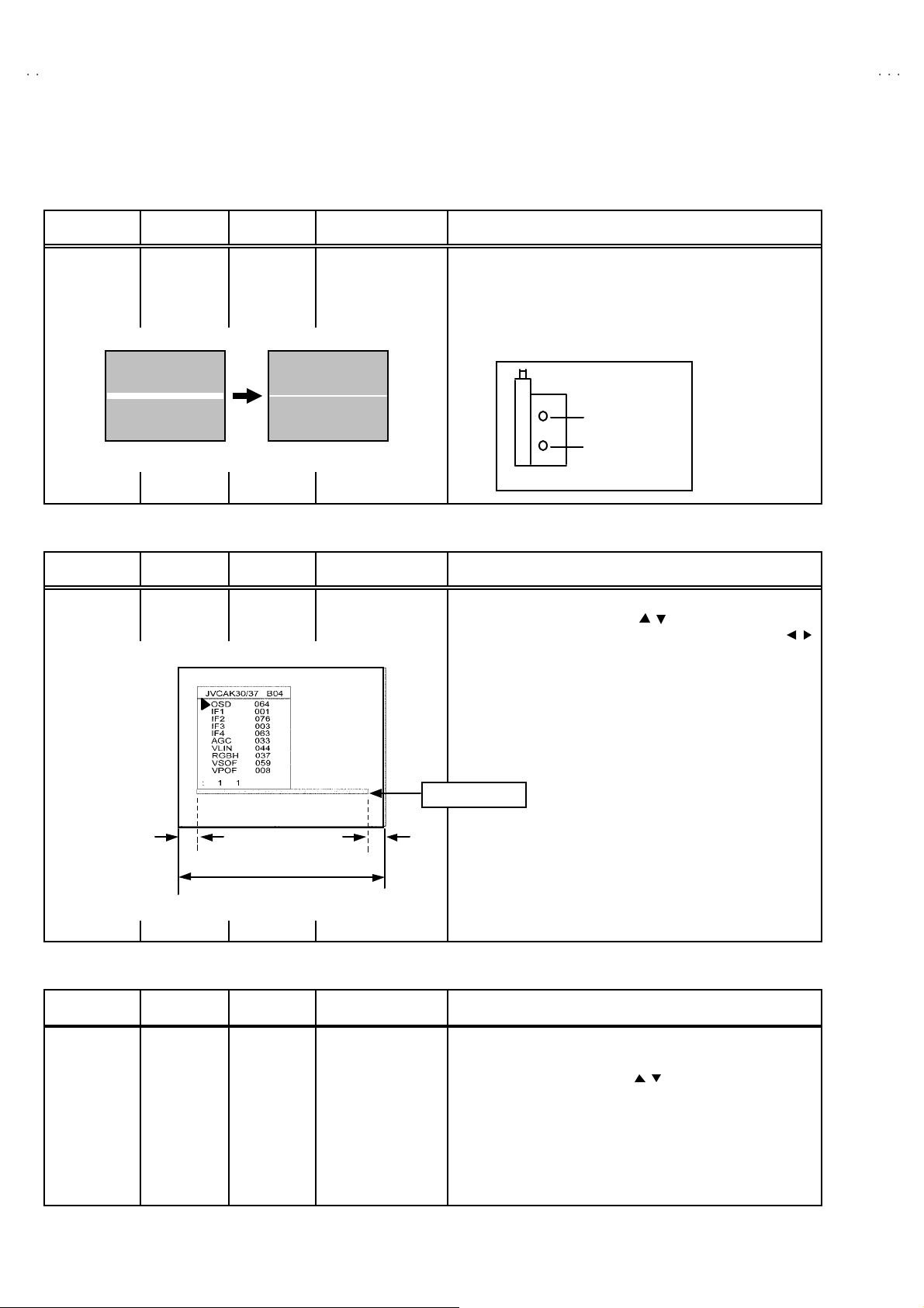
■■■■ SCREEN ADJUSTM ENT
Item
SCREEN
adjust me nt
■■■■ OSD HORIZONTAL POSITION AD JUSTMENT
Item
HORI ZONTAL
POSITION O F
OSD
adjust me nt
Measuring
instrume nt
Remote
control unit
Measuring
instrume nt
Remote
control unit
Test point Ad justment part Description
SCREEN VR
[On the FBT]
Test point Ad justment part Description
OSD 1. En ter SE R VIC E M ENU.
SE RVICE MENU SCREEN
1. En ter SE R VICE MENU .
2. Press YEL LOW ke y to disab l e ve rt ic al s can .
3. Ad ju st SC R EE N VR. on the F BT a s th in as pos sible.
4. Pr ess YELLOW k ey ag ai n to en able v er ti cal sc an.
5. Pr ess STANDARD key t o le ave s ervic e m en u.
FOCUS VR
SCR EEN VR
FBT
2. Select OSD with FUNCTION ( / ) key
3. Adjust the OSD horizontal position with the FUNCTION ( / )
key, wh ic h shifts th e ref er enc e bar on the b ott om of th e
SE RV ICE MENU ho r izo ntall y, s o th at the OSD is po sition ed on
th e scr een c ent er . ( X=X’)
■■■■
IF ADJUSTMENT
Item
IF adjustme nt R emot e
Measuring
instrume nt
control unit
Reference bar
XX’
Test point Ad justment part Description
IF 1
IF 2
IF 3
IF 4
1. Receive a PAL colour bar pattern.
2. En ter SE R VICE MENU .
3. Select I F 1 with FUNCTION ( / ) ke y
4. Pr ess BLUE k ey d ur i ng I F 1 is h ig hl i gh ted , I F 1 and IF 2 values
are ad ju s ted autom atic ally by sof twar e.
5. If the st and ar d i s L- p ri m e, IF 3 and I F 4 valu es are ad ju stm ent
au tom at ic al l y when B LU E key is press ed dur i n g I F 1 i s
highlight ed.
14
No. 52056
Page 15

A
A
■■■■ AGC AUTOMAT ICALLY AD JUSTMENT
Item
AG C
AUTOMATICAL LY
adjust me nt
& check
Measuring
instrume nt
Remote
control unit
SE RVICE MENU SCREEN
Test point Ad justment part Description
AG C 1. Enter SERVICE MEN U .
■■■■ DEFLECTION CIRCUIT ADJUSTMENT
V-25BT6ENS
V-25BT6ENB
2. Receive a 60dBμV RF sign al leve l.
3. Se lect AGC with th e FU NCTION ( / ) key.
4. Press BLUE ke y on the r em ot e co ntrol unit.
5. Then the adjustment will be done automatically by software.
6. See th e AGC indica tor o n SERVICE MENU, it must b e “1” .
7. Check th at p ict ure is norm al a t 90 dB μV signal level.
:11
IF INDICATOR AGC INDICATOR NONE
Item
R GB M O DE
HORI ZONTAL
SHIFT
OFF SET
adjus tme nt
VERTICAL
SIZ E OFFSET
adjus tme nt
(60Hz)
Very close
Measuring
instrume nt
Signal
generator
Remote
control unit
A
Signal
generator
Remote
control unit
Test point Ad justment part Description
RGBH 1. Input R/G/B circle pattern sig nal via vi d eo input termin al.
2. Press AV key on the remote co ntrol u nit, for ce t he TV t o RGB
mode.
3. En ter SE R VICE MENU .
4. Se lect RGBH with th e FUNCTION ( / ) key.
5. Adjust RGBH with the FUNCTION ( / ) key u ntil the circle
B
VS OF 1. R ec ei ve a NTSC-M c r oss- hat ch pa tte r n of ve rt ic al fr equ en cy
p attern i s h orizo ntally ce ntered.( A=B)
6. Check and r ead jus t RGBH i tem if th e adjus tme nt b eco mes
imprope r aft er s om e oth er g eomet ric a djust m ents are d on e.
60Hz.
2. En ter SE R VICE MENU .
3. Se lect VSOF with the FUNCTION ( / ) key.
4. Adju st VSOF with the FUNCTION ( / ) key until the
h orizo ntal bl ac k l i nes on b ot h the u pp er a nd lower p ar t of the
p attern bec ome ver y clos e to t he u pp er and lowe r hor i zon tal
si des of pictu re size a nd ne arl y ab ou t to di sa pp ear.
5. Check and readjust VSOF item if the adjustment becomes
imprope r aft er s om e oth er g eomet ric a djust m ents are d on e.
Scr e en
size
Very close
Picture
size
10 0%
No. 52056
15
Page 16

A
V-25BT6ENS
A
g
V-25BT6ENB
Item
VERTICAL
POSITION
OFF SET
Ad j ust men t
(60Hz)
HORI ZONTAL
POSITION
OFF SET
adjus tme nt
(60Hz)
Measurin
instrume nts
Signal
generator
Remote
control unit
Signal
generator
Remote
control unit
E
Test point Ad justment part Description
VPOF 1. Recei ve a N TSC-M ci rc le p att er n of ve rti ca l fr equ enc y 6 0Hz.
2. En ter SE R VICE MENU .
3. Se lect VPOF with the FUNCTION ( / ) key.
4. Adjust VPOF with t he FUNCTIO N ( / ) key until the
pictu re is vertical l y ce ntered. (C=D)
5. Check and r ead jus t vertical positi o n it em if the a djust me nt
b ecomes i m pr op er aft er s om e oth er ge ometric ad jus tm en ts
are do ne.
C
D
HPOF 1. Receive a NT SC -M circ le pat ter n sign al of vertical freq uen c y
60Hz.
2. En ter SE R VICE MENU .
3. Se lect HPOF with the FUNCTION ( / ) ke y.
4. Adjust HPOF with the FUNCTION ( / ) key until the circle
p attern i s h orizo ntally ce nte red.( E=F)
5. Check and r ea dj ust a horizo ntal posit ion it em if t he adj u stment
F
b ecomes i mp r ope r afte r so me oth er ge om etr i c adju stm en ts
are do ne.
HORI ZONTAL
TR APEZOI D
OFF SET
adjus tme nt
(60Hz)
Screen
Ver tical
Center
16
Signal
generator
Remote
control unit
Pallalel
HT O F 1. R eceive a NT SC -M cr os s-h atc h pa tter n sign al of ver tic al
fr eq ue ncy 6 0Hz.
2. En ter SE R VICE MENU .
3. Se lect HTOF with the FU NCTION ( / ) key.
4. Ad just HTOF with t he FUNCTIO N ( / ) key u ntil bo th
length s of th e up per sid e an d lo w er sid e of the c l oss- h atch
p attern b ec om e equ al.
5. Check and r eadjus t HTOF it em if the adj us tm ent bec omes
imprope r aft er s om e oth er g eomet ric a djust m ents are d on e.
No. 52056
Page 17

A
A
■■■■ GEOMETRY MENU ADJUSTMENT
g
V-25BT6ENS
V-25BT6ENB
Item
VERT ICAL
SIZ E
adjust me nt
(50Hz)
Very clos e
Scr e en
size
Very close
VERTICAL
POSITION
adjus tme nt
(50Hz)
Measurin
instrume nts
Signal
generator
Remote
control unit
Signal
generator
Remote
control unit
Test point Ad justment part Description
VS IZ 1. R eceive a PA L B/G c r oss- h atch p att er n of ver tica l f requ enc y
50Hz.
2. En ter SE R VICE MENU .
3. Press the GREEN t he n enter th e GE OMETR Y MEN U.
4. Se lect VSIZ (Vertic al size) with th e FU NCTION ( / ) key.
5. Adjust VSIZ w ith the FU NCTION ( / ) key unti l the
h orizo nt al b l ack lin es on bo th th e upp er an d low e r part of t he
p attern bec ome ver y clos e to t he u pp er and lowe r h orizo nt al
si des of pi c tu re siz e an d near ly a bout to d is appear.
6. Check and rea djus t VS IZ item i f th e ad ju s tm ent b ecomes
Picture
size
10 0%
VP OS 1. Recei v e a PAL B/G c irc le patt er n sig nal of v er t ic al f requ enc y
A
imprope r aft er s om e oth er g eomet ric a djust m ents are d on e.
50Hz.
2. En ter GE OMETRY MENU.
3. Se le c t VPOS ( Ver tica l positio n) w it h the FUNC TION ( / )
key.
4. Adjust VPOS with th e FU NCTION ( / ) ke y until t he circle
pattern is vertically centered.(A=B)
5. Check and r ead jus t VP OS i tem if th e ad ju stm en t bec omes
imprope r aft er s om e oth er g eomet ric a djust m ents are d on e.
VERTICAL
S-CORRE CTION
adjus tme nt
(50Hz)
Signal
generator
Remote
control unit
B
VS CO 1. Recei ve a PAL B/G cross-h atch p atte r n s i gn al of ver ti ca l
fr eq ue ncy 50H z.
2. En ter GE OMETRY MENU.
3. Se le c t VS CO ( Ver ti c a l s-c orrec ti on) wit h t he FUNCT ION
( / ) key.
4. Ad just VSCO with th e FU NCTION ( / ) key until the vertical
length of th e cen ter squ arer of th e cr os s- hatch p att er n
b ecomes equ al to up per a nd lower pa rt squ ar es of th e cr ossh atch pat tern .
5. C heck an d r ead jus t VS CO i te m i f t he adjustme nt bec om es
imprope r aft er s om e oth er g eomet ric a djust m ents are d on e.
No. 52056
17
Page 18

A
V-25BT6ENS
A
V-25BT6ENB
Item
VERTICAL
CORNER
CORRECTION
adjus tme nt
(50Hz)
HORI ZONTAL
SIZ E
adjus tme nt
(50Hz)
Measuring
instrume nt
Signal
generator
Remote
control unit
Signal
generator
Remote
control unit
Picture size 100%
Test point Ad justment part Description
VCCO 1. R eceive a PA L B/ G cr oss-h atc h pat ter n s i gn al of ver tic al
fr eq ue ncy 5 0Hz.
2. En ter GE OMETRY MENU.
3. Select VCCO (Vertical s-correction) with t he FUNCTION
( / ) key.
4. Ad just VCCO with t he FU NCTION ( / ) key until the vertical
length o f th e upper a nd l ow e r p ar t squ ares of t he c r oss -hatch
p attern b ec om e equ al t o each ot her.
6. Check and read jus t VCCO ite m i f the adj u s tm ent b ecomes
imprope r aft er s om e oth er g eomet ric a djust m ents are d on e.
HS IZ 1. R ec eive a PA L B/ G cross - h atch pat ter n si gn al of verti cal
fr eq ue ncy 5 0Hz.
2. En ter GE OMETRY MENU.
3. Se lect HISZ (Hor izontal size) w ith the FUNCTION ( / ) key.
4. Adjust HISZ wi th the FUNCTION ( / ) key unti l the vertical
blac k lines o n both the left and r ight p art of th e cross-h atc h
pattern become very clos e to the left and right horizontal sides
of pi ctu re tu be an d nea rly a bout t o di sapp ea r .
HORI ZONTAL
POSITION
adjus tme nt
(50Hz)
Very clos e
Signal
generator
Remote
control unit
C
Screen size
Very clos e
HPOS 1. R eceive a PA L B/ G circl e p atte rn sig nal o f ver ti c a l frequ en c y
50Hz.
2. En ter GE OMETRY MENU.
3. Select HPOS wit h the FU NCTION ( / ) key.
4. Adjust HPOS with th e FU NCTION ( / ) key u ntil th e circl e
p attern i s h orizo ntally ce nte red.( C=D)
D
5. Check and rea djus t HPOS i te m if the adju stment becom es
imprope r aft er s om e oth er g eomet ric a djust m ents are d on e.
18
No. 52056
Page 19

A
V-25BT6ENS
A
V-25BT6ENB
Item
HORI ZONTAL
PINCUSHION
adjust me nt
(50Hz)
HORI ZONTAL
CORNER
CORRECTION
adjust me nt
(50Hz)
Measuring
instrume nt
Signal
generator
Remote
control unit
Signal
generator
Remote
control unit
Test point Ad justment part Description
HPIN 1. Recei v e a PA L B/ G cross - h atch pat ter n s i gn al of ver tic al
fr eq ue ncy 5 0Hz.
2. En ter GE OMETRY MENU.
3. Se lec t H PIN(Horizo nt al pinc u s hi on ) wit h th e FUNCT ION
( / ) key.
4. Ad just HPIN with the FUNCTION ( / ) ke y until t he b ending
of the vertical line of the cross-hatch pattern are corrected.
5. Check and r ea djus t H PIN i tem if th e adju stmen t beco m es
imprope r aft er s om e oth er g eomet ric a djust m ents are d on e.
HCCO 1. Recei ve a PA L B/ G cr oss-h atc h pat ter n sign al of ve r tic al
fr eq ue ncy 5 0Hz.
2. En ter GE OMETRY MENU.
3. Select HCCO (Horizontal corner c orrection) wit h the
FUNCTION ( / ) key.
4. Ad just HCCO w ith t he FU NCTION ( / ) key until the bending
of the vertical line of the cross-hatch pattern are corrected.
5. Check and read jus t H C CO it em i f t he a djus t ment b eco me s
imprope r aft er s om e oth er g eomet ric a djust m ents are d on e.
HORI ZONTAL
TR APEZOI D
adjust me nt
(50Hz)
Screen
Ver tical
Center
Signal
generator
Remote
control unit
HT R P 1. R eceive a PA L B/ G cr oss- h atch pat ter n s i gn al of ver tic al
fr eq ue ncy 5 0Hz.
2. En ter GE OMETRY MENU.
3. Se lect HTR P ( Hor i zont al trap ezo id ) wit h t he FU NCTION
( / ) key.
4. Adjust HTRP with the FUNCTION ( / ) key until both lengths
of th e upp er sid e and lower si de of th e c r oss- hatc h pa tte rn
A
B
b ecome equ al .( A=B)
5. Check and re adjus t HT R P i te m if th e a djust ment b ec o me s
imprope r aft er s om e oth er g eomet ric a djust m ents are d on e.
No. 52056
19
Page 20

A
V-25BT6ENS
A
V-25BT6ENB
■■■■ WHITE BALANCE ADJUSTM ENT
Item
WHITE
BALANCE
adjust me nt
(Low light)
Measuring
instrume nt
Signal
generator
Remote
control unit
Test point Ad justment part Description
Recommended value 03 0 03 0 03 0
WR
WG
WB
It em WR WG W B
1. Recei ve a bla ck & wh it e sign al (col o ur off ).
2. En ter SE R VICE MENU .
3. Se lect WR / W G / W B with t he ( / ) key, res pect ive ly.
4. Ad just WR / WG / WB with t he FUNCTION ( / ) key ,
resp ecti vely, unt il th e whit e p art tu rns to pu re whit e witho ut any
other color..
WHITE
BALANCE
adjust me nt
(Hi gh light)
Signal
generator
Remote
control unit
BR
BG
It em BR BG
Recommended value 028 02 9
1. Recei ve a bla ck & wh it e sign al (col o ur off )
2. En ter SE R VICE MENU .
3. Se lect BR / BG with th e FU NCTION ( / ) key resp ect ive ly.
4. Adjust BR / BG with the FU NCTION ( / ) key resp ectively
until the white part of screen make white colour.
20
No. 52056
Page 21

A
A
PARTS LIST
CONTENTS
V-25BT6ENS
V-25BT6ENB
!
USING PW BOA RD & REMOTE CONTROL UNIT
・・・・・・・ ・・・・・・・・・・・・・ ・・・・・・・・・・・・・・・・・・・ ・・・・・・・・・・・・・・・
! EXPLODED VIEW PARTS LIST・・・・・・・ ・・・・・・・・・・・・・ ・・・・・・・・・・・・・・・・・・・ ・・・・・・・・・・・・・ ・・・・・・・・・・・・・・・・・・・・・・ 22
!
EXPLODED VIEW
!
PRINTED WIRING BOARD PARTS LIST
・・・・・・・ ・・・・・・・・・・・・・ ・・・・・・・・・・・・ ・・・・・・・・・・・・・・・・・・・・ ・・・・・・・・・・・・・・・・・・・ ・・・・・・・・・・・・・ ・・・・
[ AV-25BT6ENS / AV-25BT6ENB ]
"
MA IN PW B OARD AS S' Y
"
CRT SOC KE T PW B OARD AS S’ Y ・・・・・・・ ・・・・・・・・・・・・・ ・・・・・・・・・・・・ ・・・・・・・ ・・・・・・・・・・・・・ ・・・・・・・・・・・・・・・・・・・・・・・・・・ 28
" FRON T CONTROL PW B OAR D AS S’ Y ・・・・・・・・・・・・・・・・・・・・ ・・・・・・・・・・・・ ・・・・・・・ ・・・・・・・・・・・・・ ・・・・・・・・・・・・・・・・・・・ ・・・28
" HEADPH ON E PW B OARD AS S’Y ・・・・・・・ ・・・・・・・・・・・・・ ・・・・・・・・・・・・・・・・・・・ ・・・・・・・・・・・・・ ・・・・・・・・・・・・・・・・・・・ ・・・・・・・
!
PACKING / PACKING PART S L IS T
・・・・・・・ ・・・・・・・・・・・・・ ・・・・・・・・・・・・ ・・・・・・・・・・・・・・・・・・・・ ・・・・・・・・・・・・・・・・・・・ ・・・・・・・・・・・・・ ・・
・・・・・・・ ・・・・・・・・・・・・・ ・・・・・・・・・・・・・・・・・・・ ・・・・・・・・・・・・・・・・・・・・・・・・・ ・・・・・・
USING PW BOARD & REMOTE CONTROL UNIT
Model
PW B AS S' Y
MAIN PWB VE-2010 1572
AV-25BT6ENS AV-25BT6ENB
21
23
24
28
29
CRT SOCKET PWB
FRONT CONTROL PWB
HEADPHONE PWB
REMOTE CONTROL UNI T
VE -2 00946 70
VE -2 00845 70
VE -2 00794 93
VE -3 00177 63
(RM-C1100)
No. 52056
21
Page 22

A
V-25BT6ENS
A
V-25BT6ENB
EXPLODED VIEW PARTS LIST
!
Ref.No. Part No. Part Name Description
!
V01 VE-30002750 PICTURE TUBE (ITC)
L01 VE-30012053 DEG COIL & EARTH CB.
!
TR601 VE-30017522 FBT TRF
!
1 VE-35000013 SPRING ON/OFF SWITCH
!
2 VE-20043532 BUTTON ON/OFF (AV-25BT6ENS)
!
2 VE-20000903 BUTTON ON/OFF (AV-25BT6ENB)
3 VE-20000872 LENS
!
4 VE-20046446 FRONT CABINET (AV-25BT6ENS)
!
!
4 VE-20004131 FRONT CABINET (AV-25BT6ENB)
5 VE-40000127 SWITCH ON/OFF 2.5A/100A
!
6 VE-20043545 BUTTON FUNCTION SILVER (AV-25BT6ENS)
!
!
6 VE-20003730 BUTTON FUNCTION BLACK (AV-25BT6ENB)
7 VE-35004456 BRAC.HP/STR 6382
8 VE-30001946 SPEAKER 8R 15W (57X160) (X2)
9 VE-30015614 PFC TRF
10 VE-20086831 SHASSI BASE
!
!
11 VE-20094516 CHASSIS FRAME
!
12 VE-20092523 REAR COVER (AV-25BT6ENS)
12 VE-20101575 REAR COVER (AV-25BT6ENB)
!
13 VE-20067720 AV TARMINAL BOARD
!
14 VE-20067720 SCREW (2.9X9.5) (X4)
15 VE-35004572 SCREW (4X20) (X8)
!
16 VE-20102134 RATING LABEL (AV-25BT6ENS)
16 VE-20102164 RATING LABEL (AV-25BT6ENB)
!
17 VE-40009154 LOGO JVC (AV-25BT6ENS)
17 VE-40009152 LOGO JVC (AV-25BT6ENB)
22
No. 52056
Page 23

A
V-25BT6ENS
A
V-25BT6ENB
EXPLODED VIEW
MAIN PWB
!
10
!
TR 601
15
!
16
!
13
14
!
11
!
12
!
9
!
V01
8
FRONT
CO NTROL PWB
8
!
L01
!
!
5
17
1
2
6
7
HEADPHONE PWB
!
3
!
4
No. 52056
23
Page 24

A
V-25BT5ENS
A
V-25BT5ENB
PRINTED WIRING BOARD PARTS LIST
[ AV-25BT6ENS / AV-25BT6ENB ]
MAIN P.W. BOARD ASS’Y (VE-20101572)
Symbol No. Part No. Part Name Description
!
RESISTOR
R102 VE-30012657 SMD RES. 1/16W 1K J
R103 VE-30012657 SMD RES. 1/16W 1K J
R106 VE-30012713 SMD RES. 1/16W 75R J
R107 VE-30012649 SMD RES. 1/16W 150R J
R109 VE-30012713 SMD RES. 1/16W 75R J
R110 VE-30012713 SMD RES. 1/16W 75R J
R111 VE-30012649 SMD RES. 1/16W 150R J
R113 VE-30012713 SMD RES. 1/16W 75R J
R114 VE-30012713 SMD RES. 1/16W 75R J
R115 VE-30012713 SMD RES. 1/16W 75R J
R117 VE-30000792 CF RES. 1/4W 75R J
R118 VE-30012713 SMD RES. 1/16W 75R J
R121 VE-30012649 SMD RES. 1/16W 150R J
R122 VE-30000792 CF RES. 1/4W 75R J
R123 VE-30000792 CF RES. 1/4W 75R J
R124 VE-30012649 SMD RES. 1/16W 150R J
R126 VE-30012657 SMD RES. 1/16W 1K J
R129 VE-30012713 SMD RES. 1/16W 75R J
R135 VE-30012657 SMD RES. 1/16W 1K J
R137 VE-30000466 CF RES. 1/4W 1K J
R138 VE-30012657 SMD RES. 1/16W 1K J
R139 VE-30012713 SMD RES. 1/16W 75R J
R141 VE-30012657 SMD RES. 1/16W 1K J
R145 VE-30012713 SMD RES. 1/16W 75R J
R149 VE-30012703 SMD RES. 1/16W 56K J
R151 VE-30012696 SMD RES. 1/16W 47K J
R152 VE-30000752 CF RES. 1/4W 56K J
R153 VE-30012657 SMD RES. 1/16W 1K J
R154 VE-30000723 CF RES. 1/4W 47K J
R155 VE-30012649 SMD RES. 1/16W 150R J
R169 VE-30012703 SMD RES. 1/16W 56K J
R171 VE-30012713 SMD RES. 1/16W 75R J
R172 VE-30012692 SMD RES. 1/16W 4.7K J
R174 VE-30012713 SMD RES. 1/16W 75R J
R175 VE-30012713 SMD RES. 1/16W 75R J
R176 VE-30012703 SMD RES. 1/16W 56K J
R201 VE-30012674 SMD RES. 1/16W 27K J
R202 VE-30012692 SMD RES. 1/16W 4.7K J
R204 VE-30000459 CF RES. 1/4W 100R J
R206 VE-30000459 CF RES. 1/4W 100R J
R319 VE-30014076 SMD RES. 1/16W 4.7R J
R320 VE-30014076 SMD RES. 1/16W 4.7R J
R324 VE-30012667 SMD RES. 1/16W 220K J
R328 VE-30012649 SMD RES. 1/16W 150R J
R329 VE-30012692 SMD RES. 1/16W 4.7K J
R332 VE-30012641 SMD RES. 1/16W 10K J
R333 VE-30012702 SMD RES. 1/16W 560R J
R338 VE-30012641 SMD RES. 1/16W 10K J
R340 VE-30012644 SMD RES. 1/16W 12K J
R341 VE-30012702 SMD RES. 1/16W 560R J
R343 VE-30012659 SMD RES. 1/16W 2.2K J
R370 VE-30012669 SMD RES. 1/16W 22K J
R371 VE-30012669 SMD RES. 1/16W 22K J
R391 VE-30012696 SMD RES. 1/16W 47K J
R417 VE-30012510 SMD RES. 1/16W 100R J
R418 VE-30012510 SMD RES. 1/16W 100R J
R419 VE-30012649 SMD RES. 1/16W 150R J
R420 VE-30000466 CF RES. 1/4W 1K J
R421 VE-30012650 SMD RES. 1/16W 15K J
R422 VE-30012659 SMD RES. 1/16W 2.2K J
R423 VE-30012712 SMD RES. 1/16W 8.2K J
R425 VE-30012510 SMD RES. 1/16W 100R J
R426 VE-30012659 SMD RES. 1/16W 2.2K J
R427 VE-30012674 SMD RES. 1/16W 27K J
R428 VE-30012510 SMD RES. 1/16W 100R J
R430 VE-30012702 SMD RES. 1/16W 560R J
R431 VE-30012674 SMD RES. 1/16W 27K J
R432 VE-30012707 SMD RES. 1/16W 680R J
R433 VE-30012683 SMD RES. 1/16W 330K J
R437 VE-30000466 CF RES. 1/4W 1K J
R438 VE-30000466 CF RES. 1/4W 1K J
R439 VE-30012657 SMD RES. 1/16W 1K J
R440 VE-30012714 SMD RES. 1/16W 820R J
R441 VE-30012674 SMD RES. 1/16W 27K J
R442 VE-30000466 CF RES. 1/4W 1K J
R446 VE-30012714 SMD RES. 1/16W 820R J
R447 VE-30012714 SMD RES. 1/16W 820R J
R448 VE-30012683 SMD RES. 1/16W 330K J
R449 VE-30012659 SMD RES. 1/16W 2.2K J
Symbol No. Part No. Part Name Description
!
RESISTOR
R450 VE-30012702 SMD RES. 1/16W 560R J
R458 VE-30012510 SMD RES. 1/16W 100R J
R459 VE-30012668 SMD RES. 1/16W 220R J
R460 VE-30012668 SMD RES. 1/16W 220R J
R461 VE-30012668 SMD RES. 1/16W 220R J
R462 VE-30012510 SMD RES. 1/16W 100R J
R467 VE-30000670 CF RES. 1/4W 330K J
R468 VE-30000670 CF RES. 1/4W 330K J
R469 VE-30000628 CF RES. 1/4W 2.7K J
R471 VE-30014022 SMD RES. 1/16W 47R J
R472 VE-30012662 SMD RES. 1/16W 2.7K J
R474 VE-30012662 SMD RES. 1/16W 2.7K J
R481 VE-30000466 CF RES. 1/4W 1K J
R482 VE-30012657 SMD RES. 1/16W 1K J
R483 VE-30012657 SMD RES. 1/16W 1K J
R485 VE-30012657 SMD RES. 1/16W 1K J
R486 VE-30012657 SMD RES. 1/16W 1K J
R487 VE-30012657 SMD RES. 1/16W 1K J
R507 VE-30000466 CF RES. 1/4W 1K J
R508 VE-30012510 SMD RES. 1/16W 100R J
R509 VE-30012641 SMD RES. 1/16W 10K J
R510 VE-30012702 SMD RES. 1/16W 560R J
R511 VE-30012657 SMD RES. 1/16W 1K J
R512 VE-30000495 CF RES. 1/4W 1.2K J
R513 VE-30000459 CF RES. 1/4W 100R J
R514 VE-30000459 CF RES. 1/4W 100R J
R515 VE-30012659 SMD RES. 1/16W 2.2K J
R516 VE-30012659 SMD RES. 1/16W 2.2K J
R517 VE-30012692 SMD RES. 1/16W 4.7K J
R518 VE-30000471 CF RES. 1/4W 10K J
R519 VE-30012698 SMD RES. 1/16W 5.6K J
R525 VE-30012649 SMD RES. 1/16W 150R J
R526 VE-30012641 SMD RES. 1/16W 10K J
R527 VE-30012692 SMD RES. 1/16W 4.7K J
R528 VE-30012698 SMD RES. 1/16W 5.6K J
R529 VE-30012698 SMD RES. 1/16W 5.6K J
R530 VE-30012698 SMD RES. 1/16W 5.6K J
R532 VE-30012659 SMD RES. 1/16W 2.2K J
R533 VE-30012644 SMD RES. 1/16W 12K J
R534 VE-30000628 CF RES. 1/4W 2.7K J
R537 VE-30012641 SMD RES. 1/16W 10K J
R538 VE-30012698 SMD RES. 1/16W 5.6K J
R539 VE-30012659 SMD RES. 1/16W 2.2K J
R540 VE-30012644 SMD RES. 1/16W 12K J
R545 VE-30012644 SMD RES. 1/16W 12K J
R548 VE-30012641 SMD RES. 1/16W 10K J
R554 VE-30012641 SMD RES. 1/16W 10K J
R555 VE-30012659 SMD RES. 1/16W 2.2K J
R556 VE-30012657 SMD RES. 1/16W 1K J
R560 VE-30012674 SMD RES. 1/16W 27K J
R561 VE-30012692 SMD RES. 1/16W 4.7K J
R568 VE-30000594 CF RES. 1/4W 22K J
R572 VE-30012659 SMD RES. 1/16W 2.2K J
R573 VE-30012641 SMD RES. 1/16W 10K J
R574 VE-30012657 SMD RES. 1/16W 1K J
R603 VE-30000459 CF RES. 1/4W 100R J
R604 VE-30012510 SMD RES. 1/16W 100R J
R606 VE-30000471 CF RES. 1/4W 10K J
R607 VE-30000554 CF RES. 1/4W 180R J
R608 VE-30000859 MF RES. 1/2W 1R F
R609 VE-30000711 CF RES. 1/2W 470R J
R610 VE-30000599 CF RES. 1/4W 220K J
R611 VE-30012708 SMD RES. 1/16W 68K J
R614 VE-30012509 SMD RES. 1/16W 100K J
R616 VE-30012650 SMD RES. 1/16W 15K J
R617 VE-30000572 CF RES. 1/4W 2K J
R630 VE-30012702 SMD RES. 1/16W 560R J
R634 VE-30000633 CF RES. 1/4W 27K J
R639 VE-30000471 CF RES. 1/4W 10K J
R640 VE-30000628 CF RES. 1/4W 2.7K J
R646 VE-30000500 CF RES. 1/4W 12K J
R647 VE-30000466 CF RES. 1/4W 1K J
!
R648 VE-30001224 FUSE RES. 1/2W 0.22R J
R650 VE-30012702 SMD RES. 1/16W 560R J
R651 VE-30012668 SMD RES. 1/16W 220R J
!
R656 VE-30001230 FUSE RES. 1/2W 27R J
!
R657 VE-30001228 FUSE RES. 1/2W 2.2R J
R662 VE-30012674 SMD RES. 1/16W 27K J
R666 VE-30000815 CF RES. 1/4W 8.2K J
24
No. 52056
Page 25

A
A
!
Symbol No. Part No. Part Name Description
RESISTOR
R668 VE-30000790 CF RES. 1/4W 6.8R J
R669 VE-30012510 SMD RES. 1/16W 100R J
R670 VE-30012510 SMD RES. 1/16W 100R J
R674 VE-30012662 SMD RES. 1/16W 2.7K J
R675 VE-30001244 FUSE RES. 1/2W 0.47R J
!
R677 VE-30001124 MO RES. 3W 220R J
R678 VE-30014022 SMD RES. 1/16W 47R J
R680 VE-30000477 CF RES. 1/4W 100K J
R681 VE-30012509 SMD RES. 1/16W 100K J
R682 VE-30008856 MO RES. 2W 270R J
R683 VE-30017083 WW RES. 5W 2.2K J
R689 VE-30000718 CF RES. 1/4W 4.7K J
R690 VE-30000466 CF RES. 1/4W 1K J
R691 VE-30012696 SMD RES. 1/16W 47K J
R692 VE-30012509 SMD RES. 1/16W 100K J
R693 VE-30012708 SMD RES. 1/16W 68K J
R694 VE-30000689 CF RES. 1/4W 3.9K J
R695 VE-30000500 CF RES. 1/4W 12K J
R696-Y VE-30001350 ZENER DIODE
R697 VE-30000712 CF RES. 1/4W 470R J
R698 VE-30012657 SMD RES. 1/16W 1K J
R699 VE-30012669 SMD RES. 1/16W 22K J
R700 VE-30012649 SMD RES. 1/16W 150R J
R701 VE-30000459 CF RES. 1/4W 100R J
R703 VE-30000459 CF RES. 1/4W 100R J
R705 VE-30000459 CF RES. 1/4W 100R J
R715 VE-30012702 SMD RES. 1/16W 560R J
R717 VE-30012702 SMD RES. 1/16W 560R J
R719 VE-30012657 SMD RES. 1/16W 1K J
R721 VE-30012510 SMD RES. 1/16W 100R J
R722 VE-30012510 SMD RES. 1/16W 100R J
R723 VE-30012510 SMD RES. 1/16W 100R J
R724 VE-30012510 SMD RES. 1/16W 100R J
R801 VE-30000718 CF RES. 1/4W 4.7K J
R803 VE-30012659 SMD RES. 1/16W 2.2K J
R805 VE-30000650 CF RES. 1/4W 33R J
R806 VE-30000982 MF RES. 1/4W 4.7K J
R807 VE-30001173 MO RES. 1W 0.47R J
R809 VE-30007784 MO RES. 5W 33K J(RADIAL)
!
R810 VE-30001257 MG RES. 1/2W 4.7M J
R811 VE-30000718 CF RES. 1/4W 4.7K J
R812 VE-30012641 SMD RES. 1/16W 10K J
R813 VE-30000466 CF RES. 1/4W 1K J
R814 VE-30000466 CF RES. 1/4W 1K J
R817 VE-30000880 MF RES. 1/4W 130K F
R818 VE-30012675 SMD RES. 1/16W 2K J
R819 VE-30000526 CF RES. 1/4W 1.5K J
R828 VE-30000530 CF RES. 1/2W 15K J
R829 VE-30000530 CF RES. 1/2W 15K J
R834 VE-30001159 MO RES. 1W 0.33R J
R836 VE-30012662 SMD RES. 1/16W 2.7K J
R839 VE-30000526 CF RES. 1/4W 1.5K J
R842 VE-30014128 SMD RES. 1/16W 33R J
R844 VE-30012641 SMD RES. 1/16W 10K J
R845 VE-30012509 SMD RES. 1/16W 100K J
R846 VE-30012692 SMD RES. 1/16W 4.7K J
R847 VE-30014128 SMD RES. 1/16W 33R J
R848 VE-30012641 SMD RES. 1/16W 10K J
R849 VE-30012510 SMD RES. 1/16W 100R J
R851 VE-30000718 CF RES. 1/4W 4.7K J
R852 VE-30000650 CF RES. 1/4W 33R J
R853 VE-30012642 SMD RES. 1/16W 120K J
R855 VE-30000459 CF RES. 1/4W 100R J
R856 VE-30012694 SMD RES. 1/16W 470K J
CAPACITOR
C141 VE-30007081 EL CAP. 4.7UF 50V M (NPL)
C142 VE-30007081 EL CAP. 4.7UF 50V M (NPL)
C143 VE-30012589 SMD CAP. 4.7NF 50V K
C144 VE-30012589 SMD CAP. 4.7NF 50V K
C145 VE-30012589 SMD CAP. 4.7NF 50V K
C146 VE-30012589 SMD CAP. 4.7NF 50V K
C147 VE-30012589 SMD CAP. 4.7NF 50V K
C148 VE-30012589 SMD CAP. 4.7NF 50V K
C149 VE-30012589 SMD CAP. 4.7NF 50V K
C150 VE-30012589 SMD CAP. 4.7NF 50V K
C155 VE-30012560 SMD CAP. 100PF 50V J
C157 VE-30012560 SMD CAP. 100PF 50V J
C159 VE-30000352 EL CAP. 100UF 16V M
C160 VE-30000345 EL CAP. 10UF 50V M
C161 VE-30000345 EL CAP. 10UF 50V M
C162 VE-30012573 SMD CAP. 47PF 50V J
V-25BT5ENS
V-25BT5ENB
!
Symbol No. Part No. Part Name Description
CAPACITOR
C164 VE-30012692 SMD RES. 1/16W 4.7K J
C165 VE-30000413 EL CAP. 4.7UF 50V M
C201 VE-30000400 EL CAP. 47UF 50V M
C205 VE-30000345 EL CAP. 10UF 50V M
C206 VE-30012610 SMD CAP. 10NF 50V J
C207 VE-30012610 SMD CAP. 10NF 50V J
C230 VE-30016654 SMD CAP. 100NF 16V K R
C246 VE-30000295 CER CAP. 100NF 50V Z F
C303 VE-30000100 MKT CAP. 330NF 63V J
C305 VE-30012590 SMD CAP. 47NF 50V K
C310 VE-30000345 EL CAP. 10UF 50V M
C333 VE-30000083 MKT CAP. 150NF 63V J
C363 VE-30000083 MKT CAP. 150NF 63V J
C364 VE-30012590 SMD CAP. 47NF 50V K
C366 VE-30000407 EL CAP. 470UF 16V M
C368 VE-30012590 SMD CAP. 47NF 50V K
C404 VE-30000190 CER CAP. 100PF 50V J CH
C408 VE-30012586 SMD C AP. 22NF 50V K
C409 VE-30000345 EL CAP. 10UF 50V M
C410 VE-30000384 EL CAP. 2.2UF 50V M
C411 VE-30000345 EL CAP. 10UF 50V M
C412 VE-30016654 SMD CAP. 100NF 16V K R
C413 VE-30000362 EL CAP. 1UF 50V M
C414 VE-30012585 SMD CAP. 2.2NF 50V K R
C415 VE-30012581 SMD CAP. 1NF 50V K R
C416 VE-30000362 EL CAP. 1UF 50V M
C417 VE-30000362 EL CAP. 1UF 50V M
C418 VE-30016654 SMD CAP. 100NF 16V K R
C419 VE-30000384 EL CAP. 2.2UF 50V M
C420 VE-30000100 MKT CAP. 330NF 63V J
C422 VE-30000352 EL CAP. 100UF 16V M
C423 VE-30000352 EL CAP. 100UF 16V M
C424 VE-30000352 EL CAP. 100UF 16V M
C425 VE-30016654 SMD CAP. 100NF 16V K R
C427 VE-30016654 SMD CAP. 100NF 16V K R
C429 VE-30012589 SMD CAP. 4.7NF 50V K
C430 VE-30016654 SMD CAP. 100NF 16V K R
C431 VE-30000362 EL CAP. 1UF 50V M
C432 VE-30016654 SMD CAP. 100NF 16V K R
C433 VE-30000345 EL CAP. 10UF 50V M
C434 VE-30016654 SMD CAP. 100NF 16V K R
C435 VE-30016654 SMD CAP. 100NF 16V K R
C436 VE-30000384 EL CAP. 2.2UF 50V M
C437 VE-30016654 SMD CAP. 100NF 16V K R
C438 VE-30016654 SMD CAP. 100NF 16V K R
C439 VE-30016654 SMD CAP. 100NF 16V K R
C440 VE-30000295 CER CAP. 100NF 50V Z F
C441 VE-30012582 SMD CAP. 10NF 50V K R
C442 VE-30000362 EL CAP. 1UF 50V M
C443 VE-30000362 EL CAP. 1UF 50V M
C444 VE-30000384 EL CAP. 2.2UF 50V M
C448 VE-30012586 SMD CAP. 22NF 50V K
C449 VE-30012560 SMD CAP. 100PF 50V J
C453 VE-30000352 EL CAP. 100UF 16V M
C455 VE-30000345 EL CAP. 10UF 50V M
C459 VE-30012560 SMD CAP. 100PF 50V J
C501 VE-30016654 SMD CAP. 100NF 16V K R
C502 VE-30000400 EL CAP. 47UF 50V M
C504 VE-30016654 SMD CAP. 100NF 16V K R
C505 VE-30012589 SMD CAP. 4.7NF 50V K
C507 VE-30000345 EL CAP. 10UF 50V M
C510 VE-30016654 SMD CAP. 100NF 16V K R
C511 VE-30012566 SMD CAP. 22PF 50V J
C513 VE-30000345 EL CAP. 10UF 50V M
C514 VE-30016654 SMD CAP. 100NF 16V K R
C515 VE-30012560 SMD CAP. 100PF 50V J
C517 VE-30016654 SMD CAP. 100NF 16V K R
C518 VE-30016654 SMD CAP. 100NF 16V K R
C519 VE-30012560 SMD CAP. 100PF 50V J
C520 VE-30012560 SMD CAP. 100PF 50V J
C521 VE-30012562 SMD CAP. 15PF 50V J
C522 VE-30012562 SMD CAP. 15PF 50V J
C523 VE-30012585 SMD CAP. 2.2NF 50V K R
C524 VE-30012566 SMD CAP. 22PF 50V J
C525 VE-30012566 SMD CAP. 22PF 50V J
C526 VE-30016654 SMD CAP. 100NF 16V K R
C527 VE-30000345 EL CAP. 10UF 50V M
C529 VE-30012589 SMD CAP. 4.7NF 50V K
C530 VE-30012589 SMD CAP. 4.7NF 50V K
C532 VE-30016654 SMD CAP. 100NF 16V K R
C536 VE-30000295 CER CAP. 100NF 50V Z F
C541 VE-30000362 EL CAP. 1UF 50V M
C542 VE-30000107 MKT CAP. 47NF 250V J
C543 VE-30000431 CER CAP. 100PF 1KV M
No. 52056
25
Page 26

A
V-25BT5ENS
A
V-25BT5ENB
!
Symbol No. Part No. Part Name Description
CAPACITOR
C544 VE-30000345 EL CAP. 10UF 50V M
C547 VE-30000345 EL CAP. 10UF 50V M
C565 VE-30016654 SMD CAP. 100NF 16V K R
C566 VE-30016654 SMD CAP. 100NF 16V K R
C567 VE-30000431 CER CAP. 100PF 1KV M
C602 VE-30017319 MKT CAP. 120NF 63V J
C604 VE-30000356 EL CAP. 100UF 63V M
C605 VE-30000360 EL CAP. 1000UF 25V M
C607 VE-30012581 SMD CAP. 1NF 50V K R
!
C618 VE-30000151 MKP CAP. 3.3NF 2KV %3.5
C621 VE-30007100 MKP CAP. 10NF 1600V %3.5
!
C622 VE-30000128 MKP CAP. 10NF 630V J
!
C625 VE-30000156 MKP CAP. 430NF 250V J
C627 VE-30000167 MKP CAP. 560NF 250V J
C629 VE-30000177 MKP CAP. 820NF 250V J
C632 VE-30000100 MKT CAP. 330NF 63V J
C635 VE-30000385 EL CAP. 2.2UF 250V M
C636 VE-30000387 EL CAP. 33UF 50V M
C640 VE-30000100 MKT CAP. 330NF 63V J
C641 VE-30000090 MKT CAP. 22NF 100V J
C642 VE-30000407 EL CAP. 470UF 16V M
C644 VE-30000409 EL CAP. 470UF 25V M
C645 VE-30000090 MKT CAP. 22NF 100V J
C646 VE-30000100 MKT CAP. 330NF 63V J
C647 VE-30007748 EL CAP. 1000UF 35V M
C648 VE-30000394 EL CAP. 3.3UF 160V M
C649 VE-30000295 CER CAP. 100NF 50V Z F
C652 VE-30000330 CER CAP. 4.7NF 50V K B
C653 VE-30000107 MKT CAP. 47NF 250V J
C655 VE-30000415 EL CAP. 4.7UF 250V M
C700 VE-30012565 SMD CAP. 1.8PF 50V J CH
C701 VE-30012565 SMD CAP. 1.8PF 50V J CH
C702 VE-30012576 SMD CAP. 56PF 50V J CH
C703 VE-30012576 SMD CAP. 56PF 50V J CH
C704 VE-30012576 SMD CAP. 56PF 50V J CH
C705 VE-30000345 EL CAP. 10UF 50V M
C706 VE-30000345 EL CAP. 10UF 50V M
C708 VE-30016654 SMD CAP. 100NF 16V K R
C712 VE-30000345 EL CAP. 10UF 50V M
C713 VE-30016654 SMD CAP. 100NF 16V K R
C714 VE-30000100 MKT CAP. 330NF 63V J
C716 VE-30000100 MKT CAP. 330NF 63V J
C717 VE-30000100 MKT CAP. 330NF 63V J
C718 VE-30000100 MKT CAP. 330NF 63V J
C719 VE-30016654 SMD CAP. 100NF 16V K R
C720 VE-30000345 EL CAP. 10UF 50V M
C721 VE-30000100 MKT CAP. 330NF 63V J
C723 VE-30000100 MKT CAP. 330NF 63V J
C724 VE-30000345 EL CAP. 10UF 50V M
C729 VE-30016654 SMD CAP. 100NF 16V K R
C730 VE-30000393 EL CAP. 3.3UF 50V M
C733 VE-30000345 EL CAP. 10UF 50V M
C734 VE-30000345 EL CAP. 10UF 50V M
C735 VE-30016654 SMD CAP. 100NF 16V K R
C736 VE-30000345 EL CAP. 10UF 50V M
C737 VE-30000384 EL CAP. 2.2UF 50V M
C738 VE-30000384 EL CAP. 2.2UF 50V M
C739 VE-30000384 EL CAP. 2.2UF 50V M
C740 VE-30000384 EL CAP. 2.2UF 50V M
C741 VE-30012589 SMD CAP. 4.7NF 50V K
C742 VE-30012589 SMD CAP. 4.7NF 50V K
C745 VE-30016654 SMD CAP. 100NF 16V K R
C801 VE-30000094 MKT CAP. 220NF 275V M AC
!
C802 VE-30000094 MKT CAP. 220NF 275V M AC
!
!
C803 VE-30000433 CER CAP. 1NF 1KV M B
!
C804 VE-30000433 CER CAP. 1NF 1KV M B
C808 VE-30012590 SMD CAP. 47NF 50V K
C809 VE-30000420 EL CAP. 150UF 400V M
C810 VE-30000387 EL CAP. 33UF 50V M
C811 VE-30000161 MKP CAP. 47NF 630V J
C812 VE-30007708 CER CAP. 1NF 1KV K (PULSE)
!
C816 VE-30000440 CER CAP. 2.2NF 4KV M
C817 VE-30000198 CER CAP. 120PF 500V J SL
C818 VE-30012590 SMD CAP. 47NF 50V K
C819 VE-30012590 SMD CAP. 47NF 50V K
C822 VE-30007308 CER CAP. 220PF 1KV K (PULSE)
C826 VE-30000406 EL CAP. 47UF 250V M (HR)
C827 VE-30000411 EL CAP. 4700UF 16V M
C828 VE-30012590 SMD CAP. 47NF 50V K
C829 VE-30000407 EL CAP. 470UF 16V M
C830 VE-30000383 EL CAP. 2200UF 25V M
C832 VE-30012590 SMD CAP. 47NF 50V K
C833 VE-30000407 EL CAP. 470UF 16V M
C834 VE-30012590 SMD CAP. 47NF 50V K
!
Symbol No. Part No. Part Name Description
CAPACITOR
C835 VE-30012590 SMD CAP. 47NF 50V K
C838 VE-30000407 EL CAP. 470UF 16V M
C839 VE-30000407 EL CAP. 470UF 16V M
C840 VE-30000407 EL CAP. 470UF 16V M
C848 VE-30000407 EL CAP. 470UF 16V M
C850 VE-30000383 EL CAP. 2200UF 25V M
C851 VE-30012590 SMD CAP. 47NF 50V K
!
C852 VE-30000440 CER CAP. 2.2NF 4KV M
C857 VE-30000106 MKT CAP. 47NF 100V J
C858 VE-30007708 CER CAP. 1NF 1KV K (PULSE)
C859 VE-30009208 CER CAP. 470PF 1KV K (PULSE)
C860 VE-30000296 CER CAP. 100NF 100V Z F
C872 VE-30007708 CER CAP. 1NF 1KV K (PULSE)
TRANSF
TR600 VE-30002090 LINE DRIVER
!
TR601 VE-30017522 FBT TRF
!
TR802 VE-30018785 SMPS TRF
COIL
L101 VE-30001971 FERRITE BEAT
L102 VE-30001971 FERRITE BEAT
L106 VE-30001971 FERRITE BEAT
L108 VE-30001971 FERRITE BEAT
L109 VE-30001971 FERRITE BEAT
L110 VE-30001971 FERRITE BEAT
L111 VE-30001971 FERRITE BEAT
L112 VE-30001971 FERRITE BEAT
L113 VE-30001971 FERRITE BEAT
L114 VE-30001971 FERRITE BEAT
L115 VE-30001971 FERRITE BEAT
L116 VE-30001971 FERRITE BEAT
L117 VE-30001971 FERRITE BEAT
L201 VE-30001979 FIXED COIL 1UH
L210 VE-30001971 FERRITE BEAT
L215 VE-30001971 FERRITE BEAT
L401 VE-30001971 FERRI TE BEAT
L402 VE-30001992 FIXED COIL 10UH
L403 VE-30001971 FERRITE BEAT
L405 VE-30014048 ADJ. COIL 44MHZ
L406 VE-30001971 FERRITE BEAT
L408 VE-30001992 FIXED COIL 10UH
L501 VE-30001971 FERRITE BEAT
L502 VE-30001971 FERRITE BEAT
L503 VE-30001971 FERRITE BEAT
L504 VE-30001971 FERRITE BEAT
L600 VE-30002031 FIXED COIL 15MH
L602 VE-30002156 LINEARITY COIL 30UH
L603 VE-30002026 FIXED COIL 1MH
L700 VE-30001971 FERRITE BEAT
L701 VE-30001971 FERRITE BEAT
L702 VE-30001992 FIXED COIL 10UH
L703 VE-30001971 FERRITE BEAT
L704 VE-30001971 FERRITE BEAT
L801 VE-30002011 CHOKE COIL 150UH
L803 VE-30001992 FIXED COIL 10UH
DIODE
D105 VE-30007760 ZENER DIODE
D106 VE-30007760 ZENER DIODE
D107 VE-30007760 ZENER DIODE
D303 VE-30001329 DIODE
D405 VE-30007763 ZENER DIODE
D407 VE-30001284 DIODE
D408 VE-30001285 DIODE
D409 VE-30001284 DIODE
D413 VE-30018526 ZENER DIODE
D501 VE-30001285 DIODE
D505 VE-30001285 DIODE
D506 VE-30001284 DIODE
D512 VE-30001285 DIODE
D513 VE-30001369 ZENER DIODE
D533 VE-30001377 ZENER DIODE
D601 VE-30001329 DIODE
D603 VE-30001285 DIODE
D605 VE-30001320 DIODE
D606 VE-30001323 DIODE
D609 VE-30001318 DIODE
26
No. 52056
Page 27

A
A
!
Symbol No. Part No. Part Name Description
DIODE
D610 VE-30001318 DIODE
D613 VE-30001318 DIODE
D614 VE-30001285 DIODE
D616 VE-30003696 DIODE
D617 VE-30001318 DIODE
D651 VE-30001285 DIODE
D653 VE-30001285 DIODE
D656 VE-30007763 ZENER DIODE
D657 VE-30007763 ZENER DIODE
D658 VE-30007763 ZENER DIODE
D659 VE-30001350 ZENER DIODE
D660 VE-30001347 ZENER DIODE
D661 VE-30001350 ZENER DIODE
D700 VE-30001285 DIODE
D701 VE-30001369 ZENER DIODE
D800 VE-30001318 DIODE
D801 VE-30001372 ZENER DIODE
D802 VE-30001318 DIODE
D803 VE-30001315 DIODE
D804 VE-30001318 DIODE
D805 VE-30001315 DIODE
D806 VE-30001315 DIODE
D808 VE-20092405 DIODE.ASSY.
D809 VE-30001329 DIODE
D810 VE-30009366 DIODE
D811 VE-30009366 DIODE
D812 VE-30001285 DIODE
D889 VE-30001384 TR
!
D891 VE-30007758 BRIDGE DIODE
D892 VE-30001318 DIODE
D893 VE-30001318 DIODE
D894 VE-30001285 DIODE
D897 VE-30001329 DIODE
TRANSISTOR
Q104 VE-30001457 TR
Q106 VE-30001457 TR
Q141 VE-30001457 TR
Q142 VE-30001457 TR
Q307 VE-30001457 TR
Q316 VE-30001458 TR
Q403 VE-30001457 TR
Q404 VE-30001457 TR
Q503 VE-30001457 TR
Q504 VE-30001458 TR
Q600 VE-30001435 TR
!
Q601 VE-30001441 TR
Q602 VE-30001429 TR
Q603 VE-30001458 TR
Q604 VE-30001457 TR
Q605 VE-30001458 TR
Q700 VE-30001458 TR
Q801 VE-30001386 TR
Q802 VE-30001457 TR
Q804 VE-30001454 TR
IC
IC301 VE-30016113 IC
IC403 VE-30014521 IC
IC500 VE-20099532 IC (SERVICE)
IC501 VE-20093395 IC (MICOM)
IC601 VE-30013985 IC
IC700 VE-30013658 IC
IC800 VE-30011968 IC
IC801 VE-30015087 IC
!
IC802 VE-30001622 IC
IC803 VE-30001500 IC
IC804 VE-30001622 IC
IC818 VE-30001506 IC
V-25BT5ENS
V-25BT5ENB
!
Symbol No. Part No. Part Name Description
OTHERS
F801 VE-30001731 FUSE 2.5A
!
TH800 VE-30001270 PTC 9 OHM
!
!
TR801 VE-30002104 LINE FILTER
TU201 VE-30009637 TUNER
VR800 VE-30001064 ADJ RES. 1/10W 470R
X401 VE-30001749 XTAL
X402 VE-30015592 XTAL
X501 VE-30002851 XTAL
X700 VE-30001756 XTAL
Z401 VE-30001705 SAW FILTER
Z402 VE-30015591 SAW FI LTER
No. 52056
27
Page 28

A
V-25BT5ENS
A
V-25BT5ENB
CRT SOCKET P.W. BOARD ASS’Y (VE-20094670)
!
Symbol No. Part No. Part Name Description
RESISTOR
R900 VE-30000788 CF RES. 1/4W 6.8M J
R902 VE-30000459 CF RES. 1/4W 100R J
R903 VE-30000459 CF RES. 1/4W 100R J
R904 VE-30000459 CF RES. 1/4W 100R J
R906 VE-30000535 CF RES. 1/2W 150K J
R907 VE-30000477 CF RES. 1/4W 100K J
R908 VE-30000477 CF RES. 1/4W 100K J
R909 VE-30000525 CF RES. 1/2W 1.5K J
R910 VE-30000525 CF RES. 1/2W 1.5K J
R911 VE-30000525 CF RES. 1/2W 1.5K J
R912 VE-30000477 CF RES. 1/4W 100K J
R913 VE-30000525 CF RES. 1/2W 1.5K J
R914 VE-30001084 MO RES. 1W 1K J
R916 VE-30001170 MO RES. 1W 4.7K J
R917 VE-30001208 FUSE RES. 1W 10R J
!
R918 VE-30000471 CF RES. 1/4W 10K J
R921 VE-30000599 CF RES. 1/4W 220K J
R922 VE-30000590 CF RES. 1/4W 2.2K J
CAPACITOR
C900 VE-30000075 MKT CAP. 100NF 250V K (DC)
C902 VE-30000415 EL CAP. 4.7UF 250V M
C903 VE-30000438 CER CAP. 2.2NF 2KV
C904 VE-30000295 CER CAP. 100NF 50V Z F
C905 VE-30000234 CER CAP. 270PF 50V J SL
C906 VE-30000350 EL CAP. 10UF 250V M
C907 VE-30000075 MKT CAP. 100NF 250V K (DC)
C909 VE-30000385 EL CAP. 2.2UF 250V M
C910 VE-30000438 CER CAP. 2.2NF 2KV
C911 VE-30000433 CER CAP. 1NF 1KV M B
COIL
L900 VE-30002170 COIL
DIODE
D901 VE-30001329 DIODE
D902 VE-30001318 DIODE
D903 VE-30001329 DIODE
D904 VE-30001329 DIODE
D905 VE-30001284 DIODE
D906 VE-30001284 DIODE
D907 VE-30001284 DIODE
D908 VE-30001284 DIODE
D909 VE-30001344 ZENER DIODE
NOT1 VE-30001329 DIODE 1A/1000V 30A
TRANSISTOR
Q900 VE-30001427 TR
Q901 VE-30001454 TR
IC
IC900 VE-30008721 IC
OTHERS
PL902 VE-30001855 CRT SOCKET
!
SG901 VE-30000428 SPARK GAP 300V
SG902 VE-30000428 SPARK GAP 300V
SG903 VE-30000428 SPARK GAP 300V
SG904 VE-30000428 SPARK GAP 300V
FRONT CONTROL P.W. BOARD ASS’Y
(VE-20084570)
Symbol No. Part No. Part Name Description
!
RESISTOR
R1 VE-30000689 CF RES. 1/4W 3.9K J
R2 VE-30000526 CF RES. 1/4W 1.5K J
R3 VE-30000770 CF RES. 1/4W 680R J
R4 VE-30000712 CF RES. 1/4W 470R J
R5 VE-30000622 CF RES. 1/4W 270R J
OTHERS
LD101* VE-30001279 LED RED/GREEN
MD101 VE-30001670 PREAMPLIFIER
PL1203 VE-30001884 RCA JACK
PL1204 VE-30001882 RCA JACK
PL1205 VE-30001883 RCA JACK
S101 VE-30002181 SWITCH TACT
S102 VE-30002181 SWITCH TACT
S103 VE-30002181 SWITCH TACT
S104 VE-30002181 SWITCH TACT
S105 VE-30002181 SWITCH TACT
HEADPHONE P.W. BOARD AS S’Y (VE-20079493)
!
Symbol No. Part No. Part Name Description
RESISTOR
R113 VE-30000744 CF RES. 1/4W 560R J
R114 VE-30000744 CF RES. 1/4W 560R J
R115 VE-30000712 CF RES. 1/4W 470R J
R116 VE-30000712 CF RES. 1/4W 470R J
COIL
L103 VE-30001996 FIXED COIL 22UH Q40 K
L104 VE-30001996 FIXED COIL 22UH Q40 K
28
No. 52056
Page 29

A
A
PACKING
3
V-25BT6ENS
V-25BT6ENB
2
4
!
5 6
7
1
8
2
PACKING PARTS LIST
Ref.No. Part No. Part Name Description
!
1 VE-50028494 CARTON BOX (AV-25BT6ENS)
1 VE-50028507 CARTON BOX (AV-25BT6ENB)
2 VE-20004294 CUSHION ASS’Y
3 VE-50026637 POLY BAG (1250*1000)
4 VE-70000587 POLY BAG
5 VE-30017763 REMOTE CONTROL UNIT (RM-C1100)
!
6 VE-50028493 INST BOOK
7 BT-54013-2TK WARRANTY CARD
8 VE-20102134 LABEL (AV-25BT6ENS)
8 VE-20102164 LABEL (AV-25BT6ENB)
No. 52056
29
Page 30

A
V-25BT6ENS
A
V-25BT6ENB
Memo
30
No. 52056
Page 31

A
A
Memo
V-25BT6ENS
V-25BT6ENB
No. 52056
31
Page 32

VICTOR COMPANY OF J APAN, LIMIT ED
HOME AV NETWORK BUSINESS UNIT 12, 3-chome, Moriya-cho, Kanagawa-ku, Yokohama, Kanagawa-prefectur e, 221-8528, Japan
4
VP 0207
DP208051
Page 33

SCHEMATIC DIAGRAMS
COLOUR TELEVISION
AV-25BT6ENS
AV-25BT6ENB
CD-ROM No.SML200207
AV-25BT6ENS AV-25BT6ENB
RM-C1100 TV
CONTENTS
NOTE ON USING CIRCUIT DIAGRAMS
SEMICONDUCTOR SHAPES
BLOCK DIAGRAM
CIRCUIT DIAGRAMS
PATTERN DIAGRAMS
COPYRIGHT 2002 VICTOR COMPANY OF JAPAN, LTD.
2-1
2-2
2-3
2-5
2-21
No.52056
Jul. 2002
Page 34

AV-25BT6ENS
STANDARD CIRCUI T DIAGRAM
NOTE ON USING CIRCUIT DIAGRAMS
1.SAFETY
The components identified by the symbol and shading are
critical for safety. For continued safety replace safety critical
components only with manufactures recommend e d parts.
2.SPECIFIED VOLTAGE AND WAVEFORM VALUES
The voltage and waveform values have been measured under the
fo llowin g conditions.
(1)Input signal : Colour bar signal
(2)Setting positions of
each knob/button and
variable resistor
(3)Internal resistance of tester
:DC 20k
/V
(4)Oscil los cope sweepi ng time
:H
20µS/div
:V
5mS/div
:Others
Sweeping time is
specified
(5)Voltage values
:All DC voltage values
Sin ce th e vo l tage val ue s of si gn a l cir cuit va ry to s ome exte n t
according to adjustments, use them as reference values.
3.INDICATIONS ON THE CIRCUIT DIAGRAM
(1)Resistors
Resistance value
No unit :[
]
K
:[K
]
M
Type
No indicatio n
:Carbon resistor
OMR
:Oxide metal film resistor
MFR
:Metal film resistor
MPR
:Metal plate resistor
UNFR
:Uninflammable resistor
FR
:Fusible resistor
Composition resistor 1/2 [W] is specified as 1/2S or Comp.
(2)Capacitors
: Original setting position
when shipped
4.NOTE FOR REPAIRING SERVICE
This model's power circuit is partly different in the GND. The
difference of the GND is shown by the LIVE side GND and the
ISOLATED(NEUTRAL) side GND.Therefore, care must be
taken for the following points.
(1)Do not touch the LIVE side GND or the LIVE side GND and the
ISOLATED(NEUTRAL) side GND simultaneously. If the above
caution is not respected, an electric shock may be caused.
Therefore, make sure that the power cord is surely removed from
the receptacle when, for example, the chassis is pulled out.
(2)Do not short between the LIVE sid e GND and ISOLATED(NEUTRAL)
side GND or never measure with a measuring apparatus measure
with a measuring apparatus ( oscilloscope, etc.) the LIVE side GND
and ISOLATED(NEUTRAL) side GND at the same time.
If the above precaution is not respected , a fuse or any parts will be broken.
Since the circuit diagram is a standa rd one, the ci rcuit and
circuit constants may be subject to change for i mpro vement
without any notice.
NOTE
Due improvement in performance, some part numbers show
in the circuit diagram may not agree with those i ndi cate d in
the part list.
When ordering part s, plea se us e the numbers that appear
in the Parts List.
Type
MM
:M eta l iz ed my lar cap ac i tor
PP
:Polypropylene ca pacitor
MPP
:Metalized polypropylene capacitor
MF
:Metalized film capacitor
TF
:Thin film capacitor
BP
:Bipolar electrolytic capacitor
TAN
:Tantalum capacitor
(3)Coils
No unit
:[
µ
H]
Others
:As specified
:[M ]
Capacitance value
1 or higher :[pF]
less than 1
:[µF]
Withstand voltage
No indication :DC50[V]
Others :DC withstand voltage [V]
AC indicated
:AC withstand voltage [V]
Electrolytic Capacitors
47/50[Example]:Capacitance value [µF]/withstand voltage[V]
No indication
:Ceramic capacitor
AV-25BT6ENS, AV-25BT6ENB
AV-25BT6ENB
FRONT CONTROL PWB PATTERN
2-24
No.52056
TOP
VP0207
DP6060
AV-25BT6ENS
AV-25BT6ENB
Jul. 2002 No. 52056
Page 35

AV-25BT6ENS
AV-25BT6ENB
CONTENTS
AV-25BT6ENS
AV-25BT6ENB
CRT SOCKET PWB PATTERN
SEMICONDUCTOR SHAPES
BLOCK DIAGRAM
CIRCUIT DIAGRAMS
MAIN PWB CIRCUIT DIAGRAM
CRT SOCKET PWB CIRCUIT DIAGRAM
HEADPHONE PWB CIRCUIT DIAGRAM
FRONT CONTROL PWB CIRCUIT DIAGRAM
P ATTERN DIAGRAMS
MAIN PWB PATTERN
CRT SOCKET PWB PATTERN
HEADPHONE PWB PATTERN
FRONT CONTROL PWB PATTERN
SEMICONDUCTOR SHAPES
TRANSISTOR
BOTTOM VIE W
E
C
B
ECB
BCE
(G)(D)(S)
FRONT VIEW
ECB
ECB
TO P VI EW
CHIP TR
C
BE
2-2
2-3
2-5
2-17
2-19
2-20
2-21
2-23
2-23
2-24
TOP
IC
B O TT OM VI EW F RO N T VIEW T O P VIEW
OUT
E
IN
IN OUTE
1 N
1 N
CHIP IC
TO P VI EW
N
N
N
1
N
1
N
1
N
HEADPHONE PWB PATTERN
FRONT
2-2
No.52056No.52056
2-23
Page 36

BLOCK DIAGRAM
AV-25BT6ENS
AV-25BT6ENB
AV-25BT6ENS
AV-25BT6ENB
PLL/VST TUNER
UV1315/16
SERVICE
CONNECTOR
I2 C
STEREO SOUND
MSP34X0D/G
VIRTUAL DOLBY
QSS
MSP 3411G
IF
SUB AMP
SUBW
TDA7261
L
L
AUDIO AMP
TDA7269A
R
R
HP AMP
TDA1308
MONO
CRT
EEPROM
KEYPAD
IR
SENSOR
SMPS
MC446
08
CONTROLLER
ST92195
+150 B+
+14V
-14V
+8V
+5V
+5V STBY
SCART1
VIDEO
PROCESSOR
STV2248C
VIDEO
SWITCHING
CIRCUITS
SVHS FAV/BAV
RGB AMP
TDA6108
VER AMP
STV9306
HOR D
BU2508
RIVE
VER. DEFL.
HOR. DEFL.
FBT
No.52056
SC
ART 2
2-3 2-4
No.52056
Page 37

CIRCUIT DIAGRAMS
MAIN PWB CIRCUIT DIAGRAM [1/6]
AV-25BT6ENS
AV-25BT6ENB
AV-25BT6ENS
AV-25BT6ENB
0V
4.9V
0V
4.9V
0V
3.9V
4.8V
1.6V
4.9V
0V
1.4V
0V
1.6V
4V
4.9V
1.9V
1.8V
4.9V
1.4V
1.4V
MAIN PWB (1/6)
VE-20101572
(AV-25BT6ENS, AV-25BT6ENB)
IC501 40
3.9V
4.9V
0V
0V
0V
0.2V
1.8V
4.9V
0.9V
4.5V
6
IC501 41
5
1.6V
1.5V
0V
4.9V
0.2V
0.2V
4.9V
4.5V
0V
0V
0V
0V
0V
0V
1.6V
1.6V
0V
3.6V
0.1V
1.6V
0.2V
1.6V
1.6V
4.9V
0.1V
2.8V
2.5V 5.5V
0V
3.9V 3.5V
4.9V 4.9V 0V
23.3V
0V
0V
4.9V
4.9V
4.2V
4.9V
4.6V
No.52056 No.52056
2-5
0V
0V
2-6
Page 38

MAIN PWB CIRCUIT DIAGRAM [2/6]
AV-25BT6ENS
AV-25BT6ENB
AV-25BT6ENS
AV-25BT6ENB
MAIN PWB (2/6)
VE-20101572
(AV-25BT6ENS, AV-25BT6ENB)
15.1V
14.9V
12.1V
0V
12.1V
0V
-15.6V
2.4V
2.4V
2.3V
3V
2.5V
2.4V
2.4V
0V 12.1V
15.3V
0V
-15.6V
0V 0V 0V
0V
2.2V
1.9V
0V
3.8V
4.4V
2.9V
2.3V
3.8V
1.1V
3V
0V
4.8V
4V
3.9V
4V
0.9V
0.8V
5.5V
5.7V
7.9V
4V
0V
3.9V
IC403 48
2
IC403 47
2.3V
6
7.8V
2.8V
2.2V
3.8V
7.9V
IC403 32
3.5
No.52056
IC403 31
4
IC403 30
4
2-7 2-8
3.5V
0.1V
3.1V
2.5V
1.6V
3.8V
2.4V
1.7V
2.4V
3.1V
0V
0V
4.1V
4.1V
0.1V
4.3V
2.5V
2.5V
2.5V
4.3V
No.52056
Page 39

MAIN PWB CIRCUIT DIAGRAM [3/6]
AV-25BT6ENS
AV-25BT6ENB
AV-25BT6ENS
AV-25BT6ENB
4.9V
4V
4.8V
3.3V
7.9V
2.2V
0.1V
7.9V
0V
0.1V
MAIN PWB (3/6)
VE-20101572
(AV-25BT6ENS, AV-25BT6ENB)
7.9V
0V
No.52056 No.52056
2-9 2-10
Page 40

MAIN PWB CIRCUIT DIAGRAM [4/6]
AV-25BT6ENS
AV-25BT6ENB
AV-25BT6ENS
AV-25BT6ENB
MAIN PWB
VE-20101572
IC601 2
3
(4/6)
(AV-25BT6ENS, AV-25BT6ENB)
IC601 5
30
Q601 B
2
-0.1V
IC601 6
2
193V
0V
1300
IC601 7
60
3.9V 3.4V
3.9V
3.3V
0V
5.5V
5.5V 26.3V
5.5V
1.4V
0V 12.6V
26.9V
1.2V
12.6V 3.1V
12.6V 4.3V
6.8V
7.4V
13.6V
11.8V
0V
0V
14.7V
No.52056
-0.1V
0V
TR601 4
300
TR601 5
250
TR601 6
120
TR601 8
25
2-11 2-12
TR601 9
65
No.52056
3.6V
5.8V
0V
Page 41

MAIN PWB CIRCUIT DIAGRAM [5/6]
AV-25BT6ENS
AV-25BT6ENB
AV-25BT6ENS
AV-25BT6ENB
12.2V
12.2V
9.4V
4.9V
4.9V
7.9V
0.1V
4.9V
1.1V
107.5V
2.5V
281V
0V
0V
0.6V
0V
12.5V
2.5V
MAIN PWB (5/6)
12.5V
4.9V
No.52056 No.52056
2-13
12.2V
11.1V
2.3V
0.1V
2-14
VE-20101572
(AV-25BT6ENS, AV-25BT6ENB)
Page 42

MAIN PWB CIRCUIT DIAGRAM [6/6]
AV-25BT6ENS
AV-25BT6ENB
AV-25BT6ENS
AV-25BT6ENB
1.4V
0V
0V
1.4V
0V
0V
1.4V1.4V
4.9V
0.1V
3.7V3.7V
0.1V
1.6V
0V
1.5V
0V3.7V3.7V
0V4.9V
0.1V
4.9V
0.1V
4.8V
4.2V
0V4.9V
2.5V3.7V
4V3.2V
2.4V
2.4V
3.7V3.7V
0V
3.7V3.7V
1.6V1.7V2.3V
3.6V
0V
6.8V
6.1V7.9V
2V2V4.8V0V
0V
3.7V
0.1V
3.7V
0.1V
0V
0.1V
3.7V
0.1V
3.7V
0.1V
No.52056
2-15
2-16
MAIN PWB (6/6)
VE-20101572
No.52056
(AV-25BT6ENS, AV-25BT6ENB)
Page 43

CRT SOCKET PWB CIRCUIT DIAGRAM
AV-25BT6ENS
AV-25BT6ENB
AV-25BT6ENS
AV-25BT6ENB
3.8V
0V
IC900 7
150 140
2.5V 2.5V
2.5V
IC900 8
0V
4.8V
201V
IC900 9
160
132V
145V
CRT SOCKET
PL902
133V
195V
-0.9V
CRT SOCKET PWB
VE-20094670
(AV-28BT8ENS, AV-28BT8ENB)
(AV-28BT8EPS, AV-28BT8EPB)
(AV-28BT8EES, AV-28BT8EEB)
No.52056 No.52056
2-17
2-18
Page 44

HEADPHONE PWB CIRCUIT DIAGRAM
FRONT CONTROL PWB
(AV-25BT6ENS, AV-25BT6ENB)
VE-20083646
HEADPHONE PWB
VE-20079493
(AV-25BT6ENS, AV-25BT6ENB)
AV-25BT6ENS
AV-25BT6ENB
AV-25BT6ENS
AV-25BT6ENB
FRONT CONTROL PWB CIRCUIT DIAGRAM
No.52056
2-19
2-20
No.52056
Page 45

PATTERN DIAGRAMS MAIN PWB PATTERN
FRONT
AV-25BT6ENS
AV-25BT6ENB
AV-25BT6ENS
AV-25BT6ENB
No.52056 No.52056
2-21
2-22
Page 46

VICTOR COMPANY OF JAPAN, LIMITED
HOME AV NETWORK BUSINESS UNIT. 12, 3-chome, Moriya-cho, Kanagawa-ku, Yokohama, Kanagawa-prefecture, 221-8528, Japan
VP 0207
DP6060
 Loading...