

Page 1
SCHEMATIC DIAGRAMS
COLOUR TELEVISION
AV-21F9(NS)
AV-21F9
AV-21F9
++−
−
COPYRIGHT 2000 VICTOR COMPANY OF JAPAN, LTD.
No. 56037 2-1
No. 56037
Aug. 2000
Page 2

AV-21F9
2-2 No. 56037
Page 3
STANDARD CIRCUIT DIAGRAM
AV-21F9
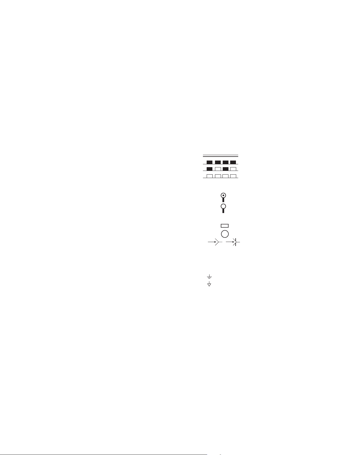
■ NOTE ON USING CIRCUIT DIAGRAMS
1. SAFETY
The components identified by the
critical for safety. For continued safety replace safety critical
components only with manufactures recommended parts.
2. SPECIFIED VOL T AGE AND W AVEFORM VALUES
The voltage and waveform values have been measured under the
following conditions.
(1)Input signal : Colour bar signal
(2)Setting positions of each knob/button and variable resistor
(3)Internal resistance of tester : DC 20kΩ/V
(4)Oscilloscope sweeping time : H ➞ 20µS/div
(5)Voltage values : All DC voltage values
* Since the voltage values of signal circuit vary to some extent
according to adjustments, use them as reference values.
3. INDICATION OF PARTS SYMBOL [EXAMPLE]
● In the PW board : R1209 ➞ R209
4. INDICATIONS ON THE CIRCUIT DIAGRAM
(1)Resistors
● Resistance value
No unit : [Ω]
K: [KΩ]
M : [MΩ]
● Rated allowable power
No indication : 1/4 [W]
Others : As specified
● Type
No indication : Carbon resistor
OMR : Oxide metal film resistor
MFR : Metal film resistor
MPR : Metal plate resistor
UNFR : Non-flammable resistor
FR : Fusible resistor
* Composition resistor 1/2 [W] is specified as 1/2S or Comp.
(2)Capacitors
● Capacitance value
1 or higher : [pF]
less than 1 : [µF]
● Withstand voltage
No indication : DC50 [V]
AC indicated : AC withstand voltage [V]
Others : DC withstand voltage [V]
* Electrolytic Capacitors
47/50 [Example]: Capacitance value [µF]/withstand voltage [V]
!!
! symbol and shading are
!!
: Original setting position when
shipped
: V ➞ 5mS/div
: Others ➞ Sweeping time is
specified.
● Type
No indication : Ceramic capacitor
MY : Mylar capacitor
MM : Metalized mylar capacitor
PP : Polypropylene capacitor
MPP : Metalized polypropylene capacitor
MF : Metalized film capacitor
TF : Thin film capacitor
BP : Bipolar electrolytic capacitor
TAN : Tantalum capacitor
(3)Coils
No unit : [µH]
Others : As specified
(4)Power Supply
: B1
: 12V
: 9V
: 5V
* Respective voltage values are indicated.
(5)Test point
: Test point
: Only test point display
(6)Connecting method
: Connector
: Wrapping or soldering
: Receptacle
(7)Ground symbol
# : LIVE side ground
" : ISOLATED (NEUTRAL) side ground
: EARTH ground
: DIGITAL ground
5. NOTE FOR REPAIRING SERVICE
This model’s power circuit is partly different in the GND. The difference of the GND is shown by the LIVE : (#) side GND and the
ISOLATED (NEUTRAL) : (") side GND. Therefore, care must be
taken for the following points.
(1)Do not touch the LIVE side GND or the LIVE side GND and the
ISOLATED (NEUTRAL) side GND simultaneously. If the above
caution is not respected, an electric shock may be caused.
Therefore, make sure that the power cord is surely removed from
the receptacle when, for example, the chassis is pulled out.
(2)Do not short between the LIVE side GND and ISOLA TED (NEU-
TRAL) side GND or never measure with a measuring apparatus
(oscilloscope, etc.) the LIVE side GND and ISOLATED (NEUTRAL) side GND at the same time. If the above precaution is
not respected , a fuse or any parts will be broken.
● Since the circuit diagram is a standard one, the circuit and
circuit constants may be subject to change for improvement
without any notice.
No. 56037 2-3
Page 4
AV-21F9
CONTENTS
SEMICONDUCTOR SHAPES ........................................................... 2-4
BLOCK DIAGRAM ............................................................................ 2-5
CIRCUIT DIAGRAMS
MAIN PWB CIRCUIT DIAGRAM............................................................................................... 2-7
AV SW PWB CIRCUIT DIAGRAM ............................................................................................ 2-9
IF PWB CIRCUIT DIAGRAM................................................................................................... 2-11
CRT SOCKET PWB CIRCUIT DIAGRAM .............................................................................. 2-13
FRONT CONTROL PWB CIRCUIT DIAGRAM....................................................................... 2-15
PATTERN DIAGRAMS
FRONT CONTROL PWB PATTERN ....................................................................................... 2-16
MAIN PWB PATTERN ............................................................................................................. 2-17
AV SW PWB PATTERN........................................................................................................... 2-19
IF PWB PATTERN ................................................................................................................... 2-20
CRT SOCKET PWB PATTERN............................................................................................... 2-21
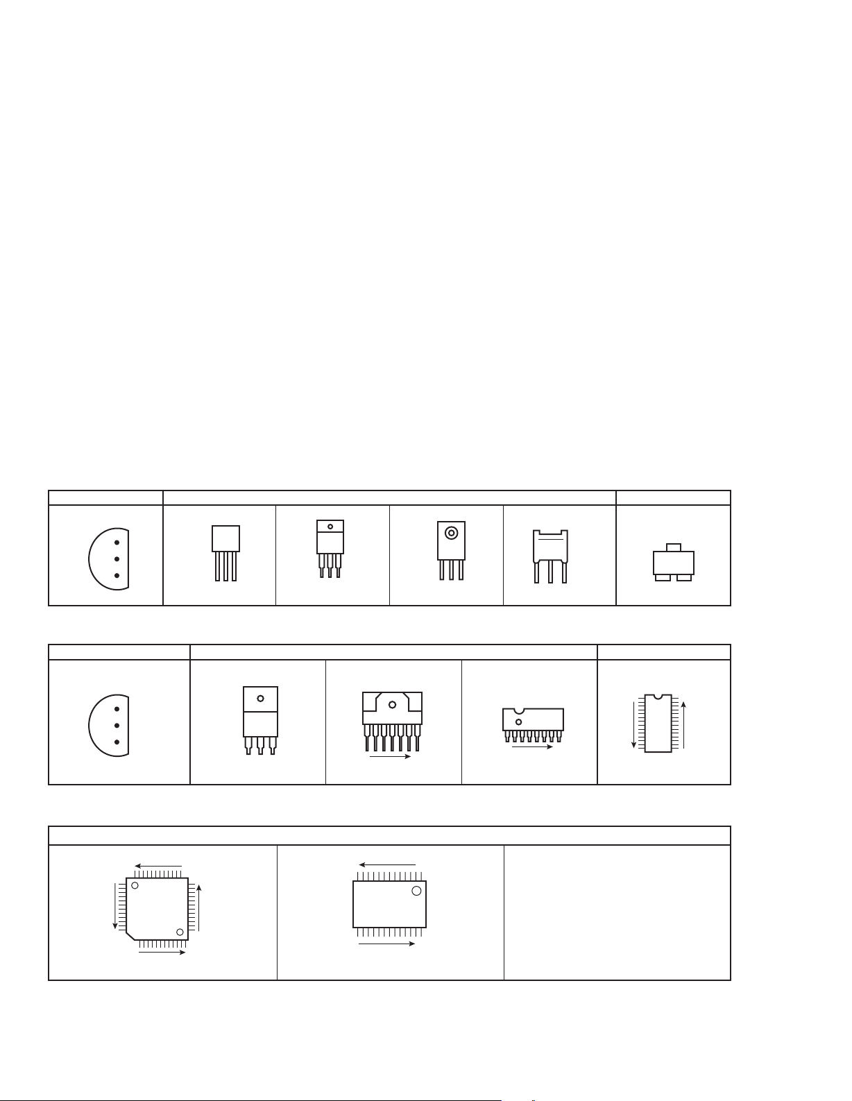
SEMICONDUCTOR SHAPES
TRANSISTOR
BOTTOM VIEW
E
C
B
IC
BOTTOM VIEW
OUT
E
IN
CHIP IC
E
CB
IN E OUT
B
(G)C(D)E(S)
FRONT VIEW
1N
TOP VIEW
TOP VIEW
CHIP TR
C
E
CB
E
CB
1N
BE
TOP VIEWFRONT VIEW
1N
N
N
N
1
N
2-4 No. 56037
1
N
Page 5
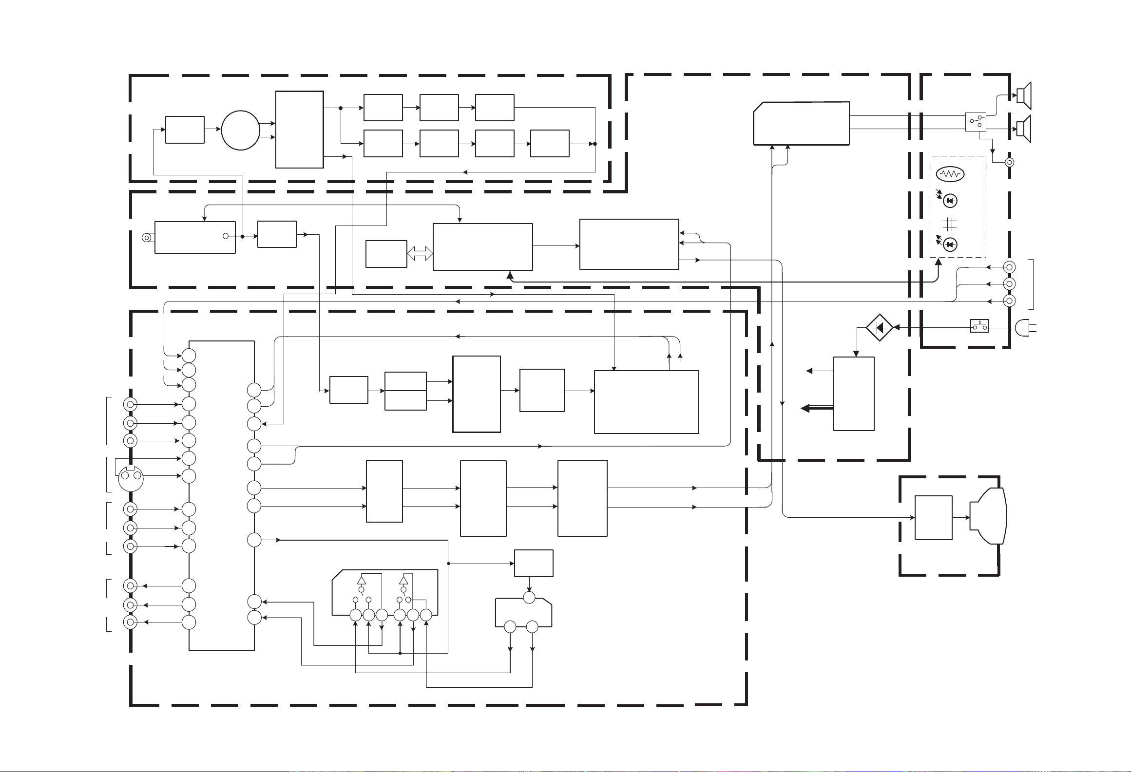
BLOCK DIAGRAM
AV-21F9 AV-21F9
IN
S/VIDEO-1
IN
VIDEO-2
S1
V1
L1
R1
V2
L2
R2
43
YC
Q101
IF AMP
TU001
IF PWB
IF
SF101
IC101
PIF/SIF/DET .
4
V.IN
5
V.IN
Q151
BUFFER
V.OUT
SIF
OUT
18
13
Q104
BUFFER
Q109
BUFFER
IC702
MEMORY
CF103
4.5
TRAP
CF106
6.0
TRAP
IC701
MICRO COMPUTER
Q103
BUFFER
CF104 5.5
CF105 6.5
TRAP
Q107
BUFFER
OSD
TV.V
IC201
V/C DEF.
PROCESSOR
MAIN PWB
42
C
Y
45
RGB
12 13 14
IC681 AUDIO AMP
L
R
113
L
R
6
8
D901
CONTROL
PWB
ECO SENSOR
KEY
IND.
POWER
FRONT
HEAD-
PHONE
FRONT
IN
VIDEO-3
V
L
R
SP01
L
SP02
R
AC IN
V
1
L
2
IC604
ALC
SF101
SF102
3
8
R
4
7
8
10
Y
C
9
11
13
TV.L
TV.R
TV.V
C.OUT
Y.OUT
L.OUT
R.OUT
48
46
47
45
43
39
38
SIF
Q101
SIF AMP
(L)
(R)
1
10
5
IC101
P.IF / S.IF
6
SELECTOR
1
19
IC601
SURROUND
Q105-Q107
17
3 (L) 11
5 (R) 6
AMP
58
IC602
VOL & TONE
SIF
60
MULTI SOUND
PROCESSOR
17 (L)
16 (R)
14
40
16
V.OUT
IC301
COMB FILTER Y/C SW
Q302
BUFFER
IC501
LR
34 33
TO REG.
B1
L
R
T921
R / G /B
RGB OUT
Q351
Q352
Q353
V01
CRT
CRT SOCKET
PWB
LINE
OUT
V
L
R
29
28
26
C.IN
IC401
VIDEO SW
Y.IN
35
37
10 11 125 7 8
AV SW PWB
NTSC COMB
FILTER
3 5
C.OUT
Y.OUT
V.IN
2
DL301
No. 56037 No. 560372-62-5
Page 6

AV-21F9 AV-21F9
CIRCUIT DIAGRAMS
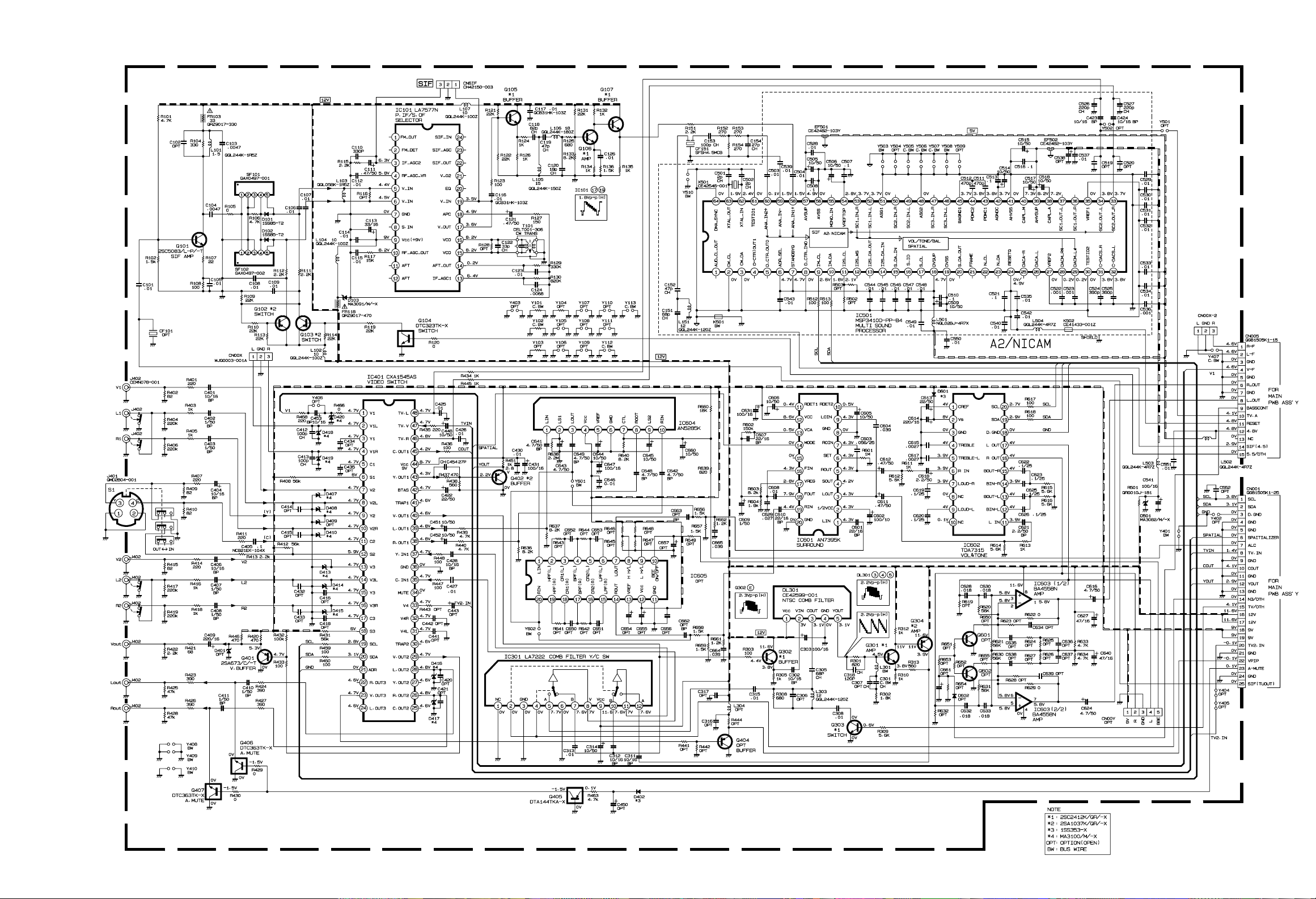
MAIN PWB CIRCUIT DIAGRAM
AV SW PWB ASS’Y
FOR FRONT CONTROL PWB ASS’Y
FOR
CRT SOCKET
PWB ASS’Y
FOR
CRT SOCKET
PWB ASS’Y
PARTS
AV21F9-NS
PARTS
AV21F9-NS
MAIN PWB ASS’Y
SCM-1617A-H2 (AV-21F9-NS)
No. 56037 2-7 No. 560372-8
Page 7
AV SW PWB CIRCUIT DIAGRAM
AV-21F9 AV-21F9
No. 56037 No. 560372-62-5
AV SW PWB ASS'Y
SCM0Y208A-H2 (AV-21F9-NS)
2-102-9
Page 8
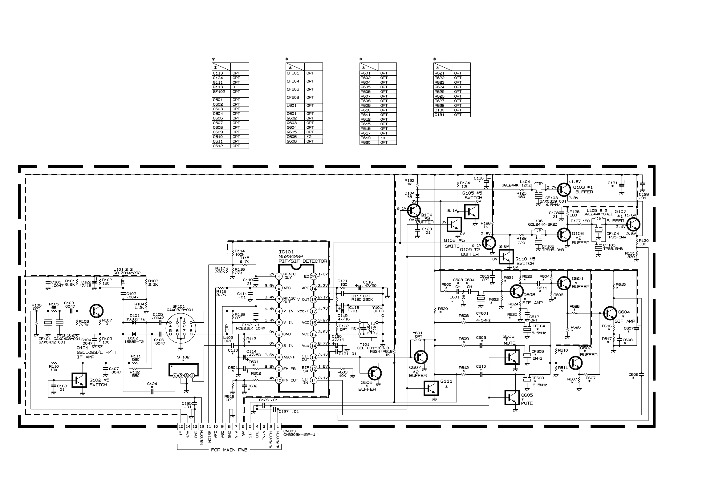
IF PWB CIRCUIT DIAGRAM
AV-21F9 AV-21F9
IF PWB ASS'Y
SCM0F201A-H2 (AV-21F9-NS)
PARTS
AV-21F9
-NS
PARTS PARTS PARTS
AV-21F9
-NS
AV-21F9
-NS
AV-21F9
-NS
No. 56037 2-7 No. 560372-8
2-122-11
Page 9

CRT SOCKET CIRCUIT DIAGRAM
AV-21F9 AV-21F9
A51LMV20X
FOR
MAIN PWB
ASS'Y
SCM-3201A-H2 (AV-21F9-NS)
PARTS
AV-21F9
-NS
FOR MAIN PWB ASS'Y
No. 56037 No. 560372-62-5
2-142-13
Page 10

AV-21F9 AV-21F9
FRONT CONTROL CIRCUIT DIAGRAM
FRONT CONTROL PWB ASS’Y
FOR
FOR
FOR
MAIN
MAIN
MAIN
PWB
PWB
PWB
ASS’Y
ASS’Y
ASS’Y
SCM-8206A-H2 (AV-21F9-NS)
PW
POWER
POWER CORD
AC110-240V
50/60Hz
QMP40D0-200J5/
QMP40D0-200J3
PATTERN DIAGRAMS
FRONT CONTROL PWB PATTERN
( )
FOR
MAIN
PWB ASS’Y
AV-21F9
-NS
FRONT
No. 56037 2-7 No. 560372-8
2-162-15
Page 11

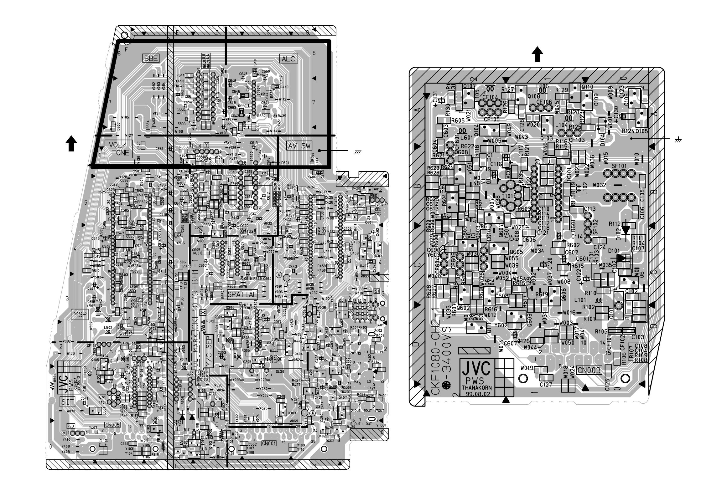
MAIN PWB PATTERN
FRONT
AV-21F9 AV-21F9
( )
TP-E
TP-91
(B1)
No. 56037 No. 560372-62-5
( )
2-182-17
Page 12
AV-21F9 AV-21F9
TOP
( )
AV SW PWB PATTERN IF PWB PATTERN
TOP
( )
No. 56037 2-7 No. 560372-8
2-202-19
Page 13

CRT SOCKET PWB PATTERN
AV-21F9
TOP
( )
No. 56037 2-21
Page 14

AV-21F9
VICTOR COMPANY OF JAPAN, LIMITED
TELEVISION RECEIVER DIVISION 1106 Heta, Iwai-city, Ibaraki-prefecture, 306-0698, Japan
No. 560372-22
Printed in Japan
CTH 0008
CRT
 Loading...