

Page 1
3
B
SERVICE MANUAL
COLOUR TELEVISION
AV-21F3
AV-21FR
AV-21FMG3
BASIC CHASSIS
AV-21F3
AV-21FR3
AV-21FMG3B
[ RM -C9 0 ]
[ RM-C3 64GY]
[RM-C 364]
CG
CONTENTS
! SPECIFICATIONS ・・・・・・・・・・・・・・・・・・・・・・・・・・・・・・・・
! SAFE TY PRECAUT IONS ・・・・・・・・・・・・・・・・・・・・・・・・・・・・・・・・
!
FEATURES・・・・・・・・・・・・・・・・・・・・・・・・・・・・・・・・
! FUNCTIONS ・・・・・・・・・・・・・・・・・・・・・・・・・・・・・・・・
!
MAIN DIFFERENCE LIST
!
SPECIFIC SERVICE INSTRUCTIONS
! SERVICE ADJUSTMENTS ・・・・・・・・・・・・・・・・・・・・・・・・・・・・・・・・
!
PARTS LIST
★
OPERATING INSTRUCTIONS
★
STAND ARD CIRCUIT DIAGRAM
1
・・・・・・・・・・・・・・・・・・・・・・・・・・・・・・・・・・・・・・・・・・・・・・・・・・・・・・・・・・・・・・・・
・・・・・・・・・・・・・・・・・・・・・・・・・・・・・・・・・・・・・・・・・・・・・・・・・・・・・・・・・・・・・・・・
・・・・・・・・・・・・・・・・・・・・・・・・・・・・・・・・・・・・・・・・・・・・・・・・・・・・・・・・・・・・・
・・・・・・・・・・・・・・・・・・・・・・・・・・・・・・・・・・・・・・・・・・・・・・・・・・・・・・・・・・・・・・・・
・・・・・・・・・・・・・・・・・・・・・・・・・・・・・・・・・・・・・・・・・・・・・・・・・・・・・・・
・・・・・・・・・・・・・・・・・・・・・・・・・・・・・・・・・・・・・・・・・・・・・・・・・・・・・・・・・・・・・・・・
・・・・・・・・・・・・・・・・・・・・・・・・・・・・・・・・・・・
・・・・・・・・・・・・・・・・・・・・・・・・・・・・・・・・・・・・・・・・・・・・・・・・・・・・・・・・・・・・・・・・
・・・・・・・・・・・・・・・・・・・・・・・・・・・・・・・・・・・・・・・・・・・・・・・・・・・・・・・・・・・・・・・・
・・・・・・・・・・・・・・・・・・・・・・・・・・・・・・・・・・・・・・・・・・・・・・・・・・・・・・・・・・・・・・・・
・・・・・・・・・・・・・・・・・・・・・・・・・・・・・・・・
・・・・・・・・・・・・・・・・・・・・・・・・・・・・・・・・・・・・・・・・・・・・・・・・・・・・・・・
・・・・・・・・・・・・・・・・・・・・・・・・・・・・・・・・・・・・・・・・・・・・・・・・・・・・・・・・・・・・・・・・
・・・・・・・・・・・・・・・・・・・・・・・・・・・・・・・・
・・・・・・・・・・・・・・・・・・・・・・・・・・・・・・・・・・・・・・・・・・・・・
・・・・・・・・・・・・・・・・・・・・・・・・・・・・・・・・・・・・・・・・・・・・・・・・・・・・・・・・・・・・・・・・
・・・・・・・・・・・・・・・・・・・・・・・・・・・・・・・・・・・・・・・・・・・・・・・・・・・・・
・・・・・・・・・・・・・・・・・・・・・・・・・・・・・・・・・・・・・・・・・・・・・・・・・・・・・・・・・・・・・・・・
・・・・・・・・・・・・・・・・・・・・・・・・・・・・・・・・
・・・・・・・・・・・・・・・・・・・・・・・・・・・・・・・・・・・・・・・・・・・・・・・・・・・・・・・・・・・・・・・・
・・・・・・・・・・・・・・・・・・・・・・・・・・・・・・・・・・・・・・・・・・・・・・・・・・・・・・・・・・・・・・・・
・・・・・・・・・・・・・・・・・・・・・・・・・・・・・・・・
・・・・・・・・・・・・・・・・・・・・・・・・・・・・・・・・・・・・・・・・・・・・・・・・
・・・・・・・・・・・・・・・・・・・・・・・・・・・・・・・・・・・・・・・・・・・・・・・・・・・・・・・・・・・・・・・・
COPYRIGHT © 2002 VICTOR COMPANY OF JAPAN, LTD.
・・・・・・・・・・・・・・・・・・・・・・・・・・・・・ 2
・・・・・・・・・・・・・・・・・・・・・・・・・・・・・・・・・・・・・・・・・・・・・・・・・・・・・・・・・・
・・・・・・・・・・・・・・・・・・・・・・・ 3
・・・・・・・・・・・・・・・・・・・・・・・・・・・・・・・・・・・・・・・・・・・・・・
・・・・・・・・・・・・・・・・・・・・・・・・・・・・・・・・・・
・・・・・・・・・・・・・・・・・・・・・・・・・・・・・・・・・・・・・・・・・・・・・・・・・・・・・・・・・・・・・・・・
・・・・・・・・・・・・・・・・・・・・・・・
・・・・・・・・・・・・・・・・・・・・・・・・・・・・・・・・・・・・・・・・・・・・・・
・・・・・・・・・・・・・
・・・・・・・・・・・・・・・・・・・・・・・・・・
・・・・・・・・・・・・・・・・・・・・・ 15
・・・・・・・・・・・・・・・・・・・・・・・・・・・・・・・・・・・・・・・・・・
・・・・・・・・・・・・・・・・・・・・・・・・・・・・・・・・・・・・
・・・・・・・・・・・・・・・・・・・・・・・・・・・・・・・・・・・・・・・・・・・・・・・・・・・・・・・・・・・・・・・・
・・・・・・・・・・・・・・・・
・・・・・・・・・・・・・・・・・・・・・・・・・・・・・・・・
・・・ 4
・・・・・・
・・ 5
・・・・
33
2-1
7
8
No. 52024
Jun. 2002
Page 2
A
V-21F3
A
A
V-21FR3
V-21FMG3B
SPECIFICATIONS
ITEM
Dimen sions( W×H×D) 619mm×458mm×486.5mm
Mass 22kg
TV RF Syst em B/ G, I, D/K B/ G, I, D/K, M
Colour System
Telet ext System FLOP (Only for AV-21FR3) ×
Pi ctur e Tube
High Voltage 26.5kV±1.5kV(at zero beam current)
Receiving Frequency VHF (VL) 46.25MHz~168.25MHz
Intermediate
Frequen cy
Col ou r S ub C arr ier Fr e q uen cy
RF Mode PAL / SECAM PAL / SECAM / NTSC3.58 / NTSC4.43
VIDEO Mode PAL / SECAM / NTSC3.58 / NTSC4.43
Visible size: 51cm measured diagonally
VHF (VH) 175.25MHz~463.25MHz
UHF 471.25MHz~863.25MHz
Cable TVs of Mid (X-Z, S1-S10)
CATV
VIF Carrier 38.0MHz
SIF Carrier
Super (S11-S20) & Hyper (S21-S41)
bands recei vable
32.5MHz (5.5MHz)
31.5MHz (6.5MHz)
32.0MHz
PAL (4.43MHz),
SECAM (4.40625MHz / 4.25MHz)
NTSC (3.58MHz / 4.43MHz)
AV - 21 F3
AV - 21 FR3
(6.0MHz)
CONTENTS
AV-21FMG3B
32.5MHz(5.5MHz) /33.5MHz (4.5MHz)
31.5MHz (6.5MHz)
32.0MHz
(6.0MHz)
Power Input Rated Voltage
Power Co nsumpti on
Speaker
Audio Output
Aer ial In pu t Termi n al
Input
Output Video 1V(p-p), 75
Headphone jack 3.5mm mini jack
Remote Control Unit
Video 1V(p-p), 75Ω (Front / Rear )
Audio
Audio 500mV(rms) (-4dBs), Low impedance,
AC110~240V, 50 / 6 0Hz
90W (Max) / 60W(Avg)
6cm×12 cm, Oval type×2
3W (monaural )
75Ω Unbalanced
500mV(rms) (-4dBs), High impedance,
RCA×2 (Front / Rear)
Ω
[AV-21F3]
: RM-C364G Y
[AV-21FR3]
: RM-C90
(Batter y size : AA / R06 / UM- 3×2)
Design and specifications are subject to change without notice.
RM-C3 64
(Batter y size : AA / R06 / UM- 3×2)
2
No. 52024
Page 3
A
3
A
A
SAFETY PRECAUTIONS
V-21F
V-21FR3
V-21FMG3B
1. The d es ign of th is prod uct c on ta ins sp eci al har d wa re , many
circuit s and components specially for safety purp oses. For
con tinu ed pr ot ection , n o c han g es sh ou ld b e ma de to the o ri g i nal
d esi gn un less auth or ized in w riti n g by th e ma nu fact urer.
Replacem en t par ts must b e id ent ic al to thos e u sed in th e or i gi n al
ci rcu its. Servi ce sho ul d b e per formed by qu alif ied p ers on nel
on ly.
2. Alte rati on s of t he des i g n or circui tr y of t he pr od ucts s h oul d not be
made. Any design alterations or additions will void the
manu fact ur er 's warrant y and w ill f urth er r el i eve t he manu factu rer
of r esp onsi b ility for perso na l injury or pr op erty dam ag e r es ult in g
th erefr om.
3. M an y electr i c al an d m ech anic a l p ar ts in th e prod ucts ha ve
special safety-related characteristics. These characteristics are
oft en not e v iden t f rom vi sual insp ec ti on n or c a n t he pro tec t io n
aff or de d by th em nec e ssar i l y be ob tai n ed b y u sing rep lacem en t
com po ne nts ra ted f or hig he r voltag e, w att ag e, etc. Rep lacem en t
p arts whic h ha ve th ese sp eci al s afet y charact erist ics ar e
ide ntified i n the parts li st of S ervice manual. El ectric al
components having such features are ide ntified by shading
on t h e sche mat ics and by (!!!! ) on the parts list in Service
manual. T he us e of a sub sti tu te rep lacem en t whic h do es n ot
h ave th e s ame saf ety ch ar act erist ics as t he reco mm en de d
replac em ent part sh own i n th e parts li st of Ser v ice m an ual m ay
cause shock, fire, or other hazards .
4. Do n't short between the LIVE s ide ground and ISOLATED
(NE UTRAL) side ground or EARTH side ground when
repairing.
Some model's power circuit is partly different in the GND. The
diff er enc e of th e GND is s ho wn b y th e LIV E : ( ") side GN D, the
ISO LATE D(N EUTRAL) : (#) si de GND and EARTH : ( $) side
GND. Do n't s h or t bet we en th e LIV E sid e GN D an d
ISO LATE D(N EUTRAL) side GND or EART H side GND an d
n ever m ea sur e w it h a mea sur ing a ppa ratus ( os cil lo scop e etc.)
th e LI VE si d e GND an d IS OLA TED(N E UTRAL ) sid e G ND or
EARTH side GND at the s ame time.
If above not e will not be kept, a fuse or any parts will be broken.
5. If any repair has been made to the chassis, it is recommended
th at t he B1 set ting shou l d b e c h ecke d or adj u ste d ( See
ADJUST M ENT OF B 1 POW E R SUPPL Y).
6. The hi gh v ol ta ge applie d t o th e pi ctu r e tube mu st con form with
th at s p ec ifi ed i n S er v ice m an ual. E xcess ive h igh vo lt ag e ca n
cau s e an i ncre ase in X-Ray em i ssi on , ar c i ng an d possib le
component damage, therefore operation under excessive high
voltage conditions should be kept to a minimum, or should be
preve nt ed. If s ever e arc ing occur s, r em ove t he AC power
immed i ate ly and de termine th e cause b y visua l insp ect ion
(inc or r ect install at ion, cr ac ke d or mel te d high vo lt age har n ess,
p oor so lder i ng, et c.) . T o m ai nt ain the p r ope r mi n im u m le vel of
sof t X- R ay emis si on, c omp on ents in th e high voltag e cir c uitr y
incl ud i ng t he pict ur e tube must b e t he exac t r ep l aceme nts or
alte rn at ives ap prov e d b y th e manuf act ur er of th e c omplet e
prod uct.
7. Do n ot c hec k high volt ag e by drawing an ar c. Use a hi gh volt ag e
meter or a hi g h v ol tag e probe wit h a V TVM . Di s cha rge th e
picture tube before attempting meter connection, by connecting
a cl i p lead to the grou nd frame a nd conn ectin g th e oth er end of
the lead through a 10kΩ 2W resi sto r to the an od e butt on .
8. When service i s r equ ire d, ob s er ve th e or i gina l lea d dress. Ex tr a
prec aut ion sh ou ld b e given t o assure correct l ea d dress in th e
high vol tag e ci r cui t a r ea. W her e a s hor t circui t h as occ u rr e d,
th ose co mpon ent s tha t i ndi ca te ev ide nce of ove r hea ting sho ul d
b e r e pl ace d. A lwa ys use th e ma nuf act urer's r ep l acemen t
components.
9. Isolation Check
(Safety for Electrical Shock Hazard)
Af ter re-ass emb ling th e pr odu c t, alw ays per f orm an i solat io n
ch ec k on the ex po sed me tal p ar ts of t he c abin et ( a nte nn a
ter m ina ls, video /au dio inpu t and ou tput t erminals, C on trol kn obs,
metal cabin et, s cr ew he ads, ea rph one jack, c on tr ol shaf ts, etc.)
to be s u re the p r odu c t i s s af e t o o perate with ou t d an ger of
elect rical s hoc k.
(1) Dielectric Strength Test
The is o l ati on be tween the AC pr im a ry ci rcu it an d all me tal p arts
exp osed t o th e us er, p arti c ularly an y expos ed met al p art having a
retu rn p ath to t he chas s is should withs tan d a volt age of 3 000 V
AC (r.m.s.) for a period of one second.
(. . . . W iths tan d a vo lt ag e of 1 10 0V A C ( r .m. s .) to an ap pl ianc e
rate d up to 12 0V , an d 3 00 0V AC ( r .m. s .) to an ap pl i an ce rat ed
200V or more, for a period of one second.)
This meth od of test requires a test equipment n ot g enerall y fou nd
in t he s er vic e trade.
(2) Leakage Current Check
Plug th e AC l in e c ord d ir ect ly into the A C ou tlet (d o n ot use a lin e
isol ati o n transf orm er dur in g this check .) . Usin g a " Leakag e
Curr ent Teste r", me asure th e lea kag e current f rom each exp osed
metal p ar t of the ca bi ne t, p art icu lar l y any e x pos ed me tal p ar t
h avi ng a re turn pa th to t he ch as sis , t o a kn ow n go od eart h
grou nd (wa ter pi p e, e tc.) . An y l eaka ge cur r en t must not e x ceed
0.5mA AC (r.m.s.).
Howev e r, i n tropic al ar ea , th is mus t no t exc e ed 0.2 mA AC
(r.m.s.).
"""" Altern at e Che ck M ethod
Plug th e AC l in e c ord d ir ect ly into the A C ou tlet (d o n ot use a lin e
isol ati o n transformer during t hi s che c k.). Use an AC v o lt me ter
h avi ng 1 000 oh ms pe r volt or m ore sens it i vity in th e fo llow i ng
mann er . C on nec t a 1 50 0Ω 10W res ist or para lle led b y a 0 .15µF
AC-type c apacit or bet ween an expo sed met al pa rt and a kno wn
g ood e ar th gro un d ( wa ter pi pe , etc.). M eas ure th e AC volt ag e
acr oss th e r es ist or with th e AC vo ltm eter . Move th e r esi s tor
con nec ti on to each ex p ose d me tal par t, p art i cularly a ny exposed
metal p ar t hav in g a r etu rn pat h to the ch ass is, an d m easu re th e
AC vol tag e ac ro ss the r es ist or . Now, re vers e th e plu g in th e AC
ou tl et and repe at eac h m ea s ur em en t. An y vol t age measu red
must no t e xceed 0 .7 5V AC (r.m.s.). This c orresponds to 0.5mA
AC (r.m.s.).
Howeve r, in tropica l area, this must n ot exceed 0.3V AC ( r.m. s.) .
This corresponds to 0.2mA AC (r.m.s.).
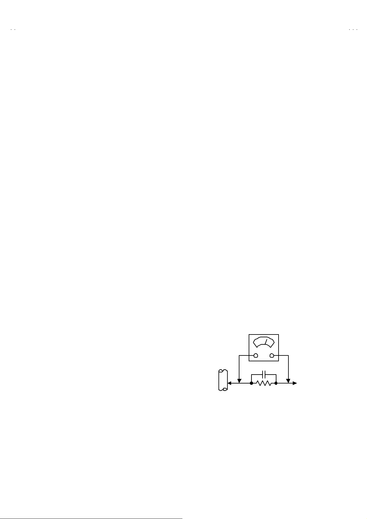
AC VOLT METER
(HAVING 1000 Ω /V,
OR MOR E SENSIT IVITY)
0.15μF AC-T YPE
PLACE THIS PROBE
1500 Ω 10W
GOOD EARTH GROUND
ON E A C H EX PO SE D
ME T AL PA RT
No.52024
3
Page 4
A
V-21F3
A
A
V-21FR3
V-21FMG3B
FEATURES
"
New c h assi s d esign enabl es us e of an int eractive on-scr ee n c ont ro l.
"
Wide ran ge volt age ( 1 10V~240V) AC power input.
" With AUDIO / VI DEO INPUT & OUTPUT te rminal.
"
MUT IN G button can r ed uce th e audi o level to z er o i nst ant l y.
" Func t ion al r em ote contr ol t o oper a te T V set (f or chann el se lect, volum e con tr ol , p ower ON /OFF , etc. ) f rom a d ist anc e.
"
I2C bu s con tr ol ut ilizes single chi p ICs for IF, V /C, DE F. VSM PR ES ET, PRESET & SETUP T OUR.
" By m eans of AUTO PR OGRA M, th e TV s tatio ns c an b e s electe d automatica lly a nd th e TV chann el s c an al so b e r ear r an ged a utom atically.
" The TELETEXT SYSTEM has a built-in FLOP system. (Only for AV-21FR3)
"
Built- in ECO MODE (ECONOMY, ECOLOGY)
In acco rdanc e with the br ig ht nes s in a roo m, th e brig ht ness and / of con tr ast of th e p ic tur e c an b e a djus t ed autom at ically to mak e the
op ti mu m pictu re whi c h is eas y on the e ye.
" Built – in ON TIMER, RETURN + & CHILD LOCK.
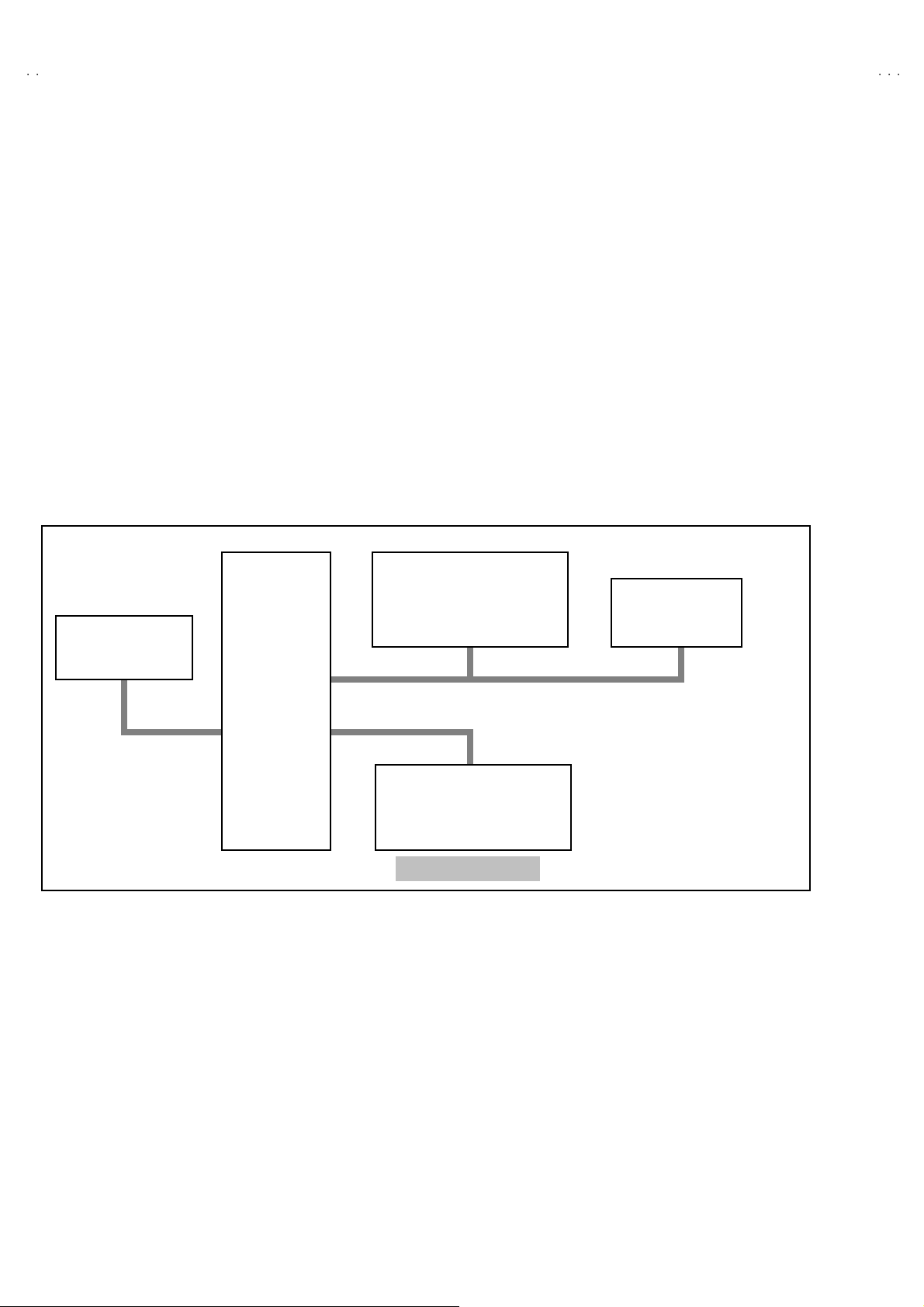
SYSTEM BLOCK DIAGRAM
"
IC702
MEMORY
IC701
SCL2/SDA2 TCL/TDA
MICRO
COMPUTER
IC301
VIDEO/CHROMA
DECORDER
SCL1/SDA1
IC821
TEXT DECORDER
Only f or AV-21FR3
TU001
TUNER
4
No. 52024
Page 5
A
3
A
A
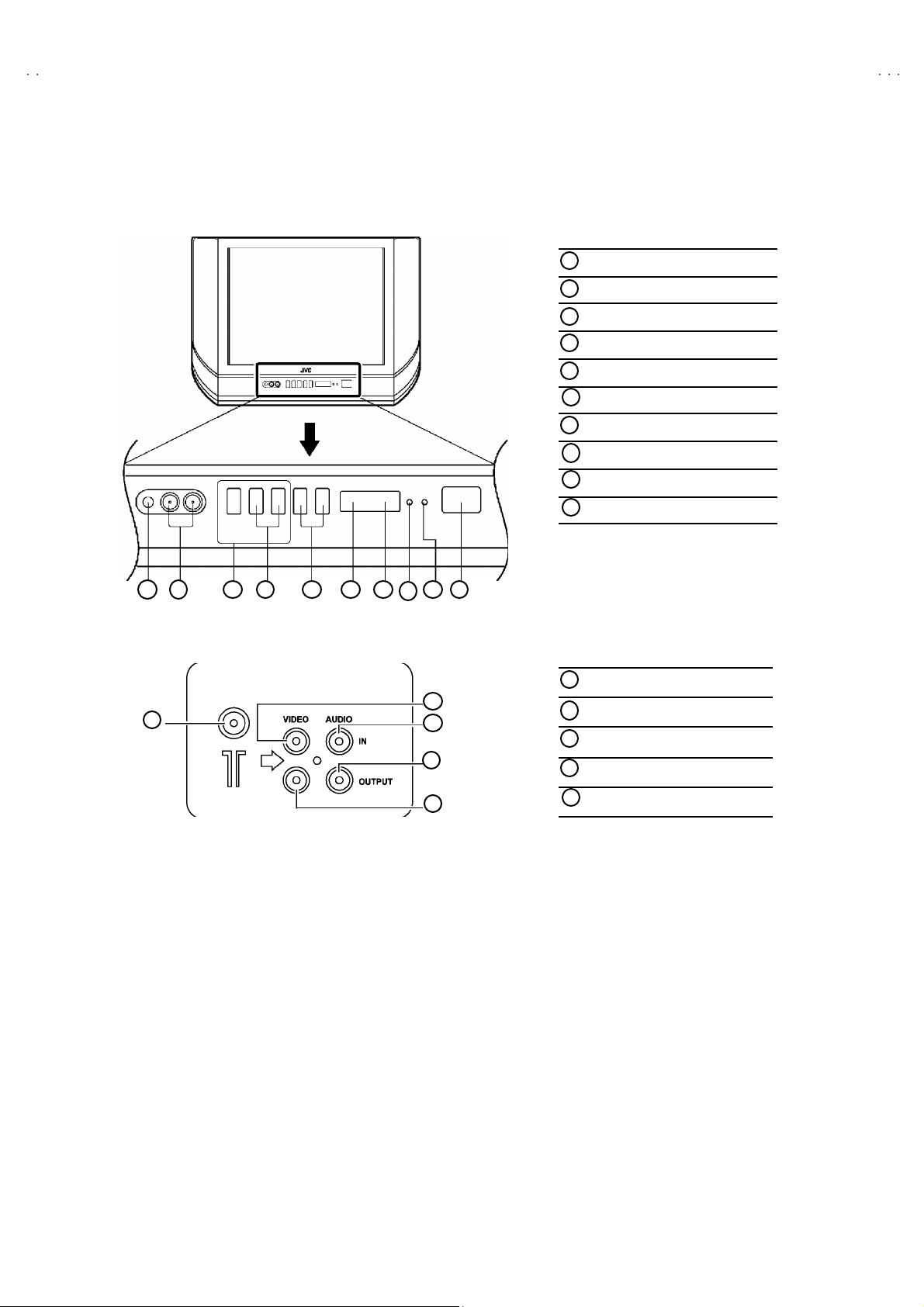
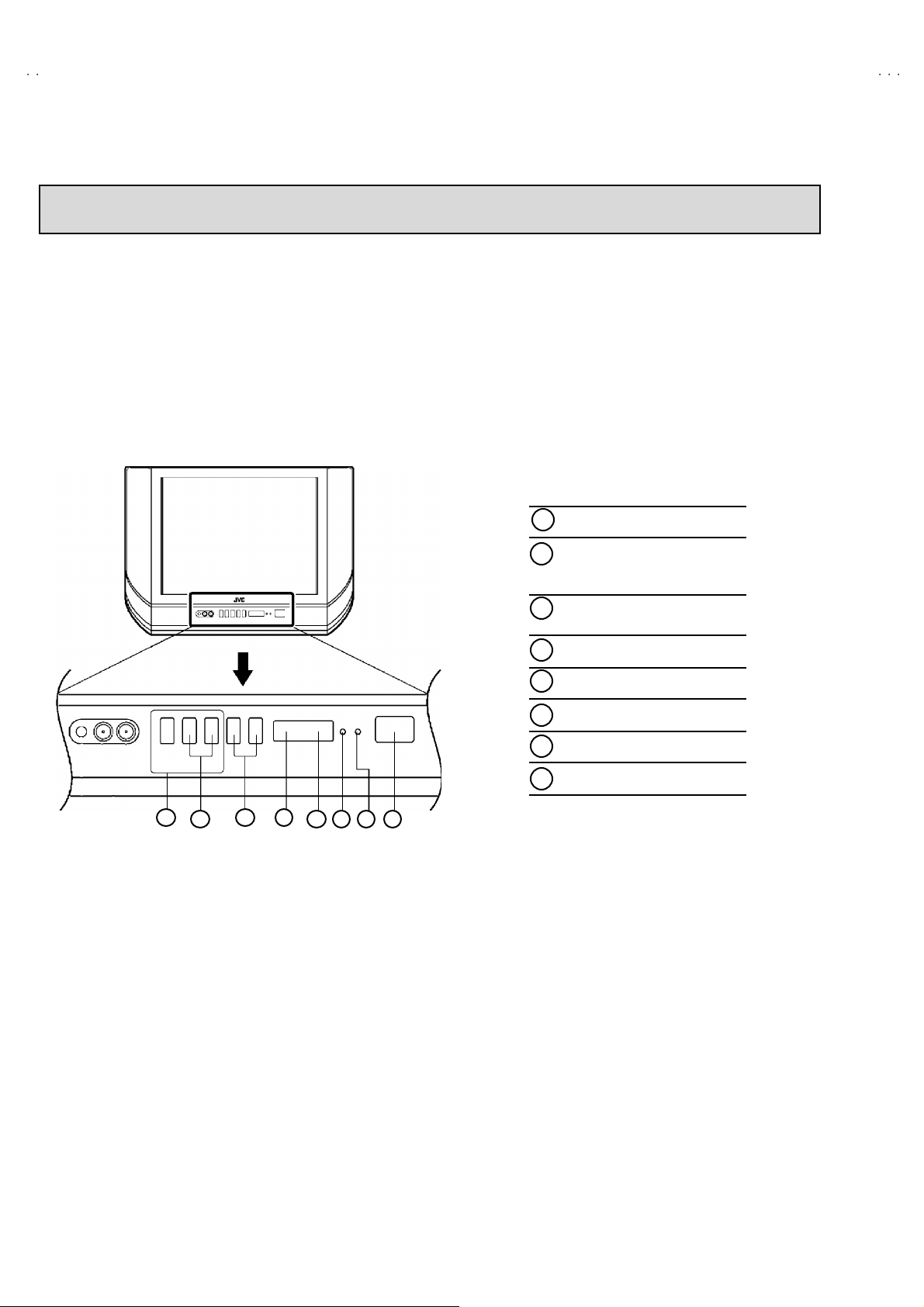
FUNCTIONS
■
FRONT PANEL
MENU buttons
1
CHANNEL -/+ buttons
2
VOLUME -/+ bu tto ns
3
AI ECO sen sor
4
REMO TE CONTR OL s ens or
5
ON TIMER lamp
6
POWER lamp
7
MAIN POWER button
8
A/V IN PUT t ermin al
9
HEAD PHONE jack
10
V-21F
V-21FR3
V-21FMG3B
10 9 1
■
REAR TERMINAL
1
3 4
2
5 6 7 8
2
3
4
5
ANT Terminal
1
VIDEO INPUT Term i nal
2
VIDEO OUTPUT Terminal
3
AUDIO INPUT T ermin al
4
AUDIO OUT PUT Terminal
5
No. 52024
5
Page 6
A
V-21F3
A
A
t
V-21FR3
V-21FMG3B
■
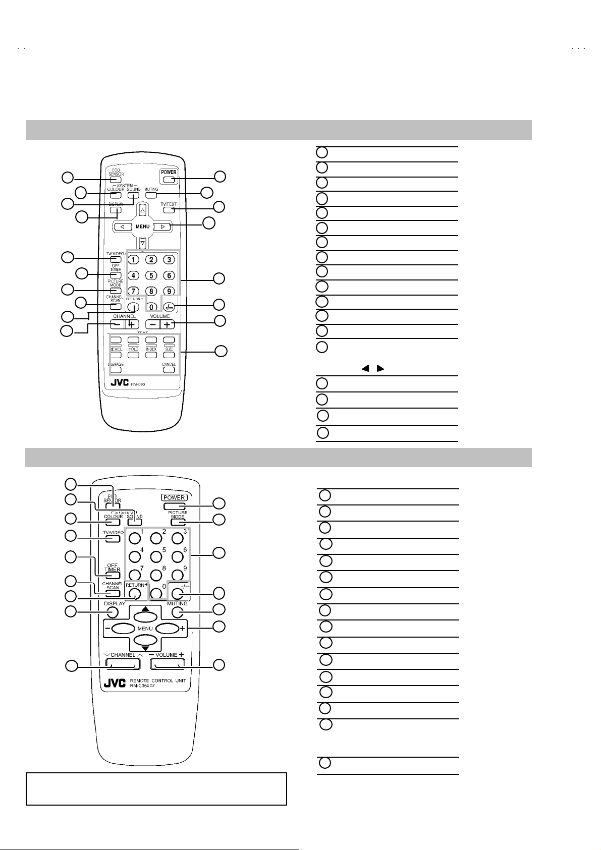
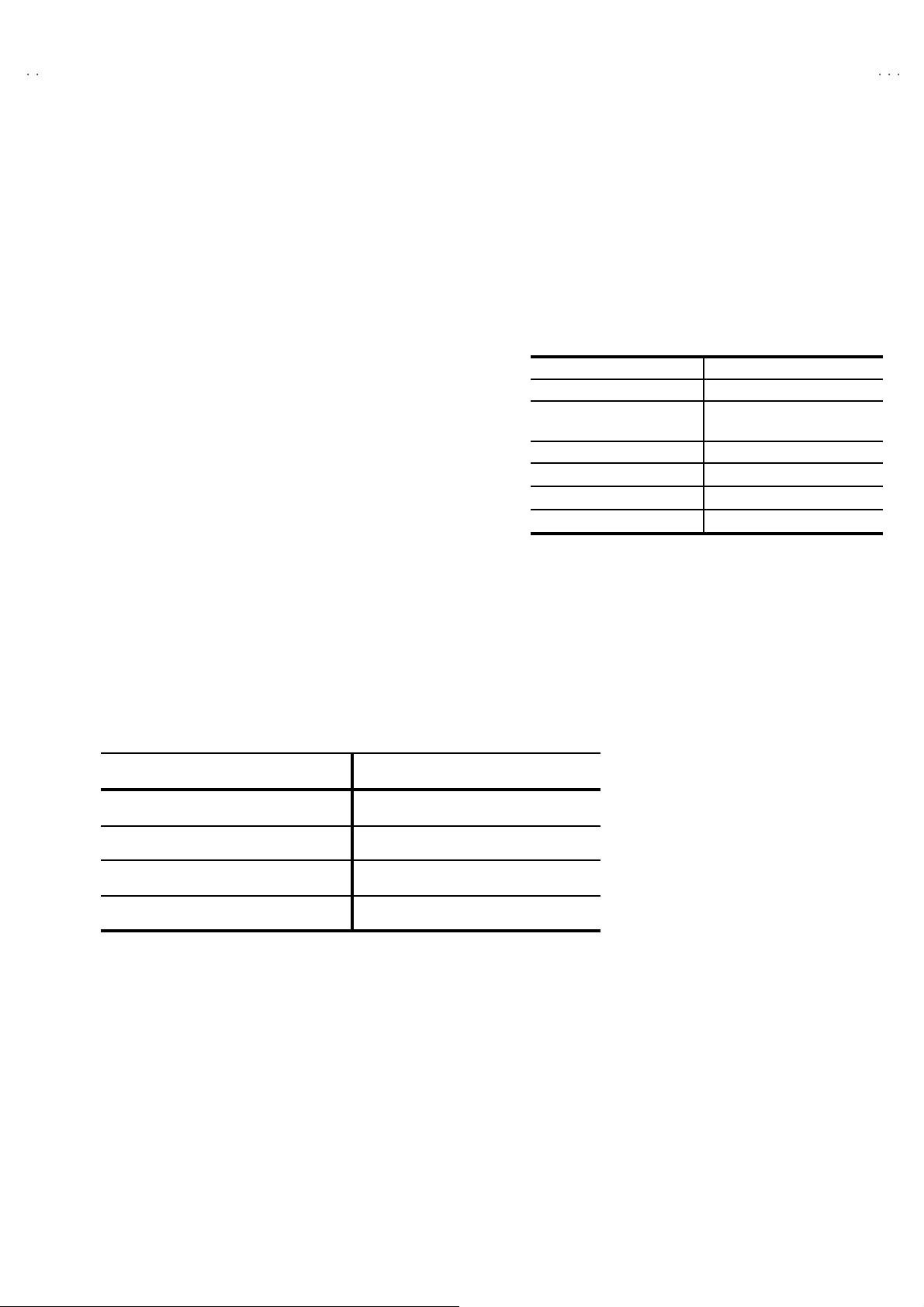
REMOTE CO NTRO L UN IT
RM-C90 : AV-21FR3
1
2
3
4
5
6
7
8
9
10
ECO S ENSOR ke y
1
COLOUR SY STEM ke y
11
12
13
14
15
16
17
18
2
SOUND SYSTEM key
3
DISPLAY key
4
TV/VI DEO key
5
OFF TIMER key
6
PICTURE MODE key
7
CHANNEL SC AN key
8
RETURN+key
9
CHANNEL -/+ key
10
POWER key
11
MUTING key
12
TV/TEXT key
13
MENU ke y
14
MENU ▲/▼ key
MENU / key
Number (CH.) key
15
-/--
16
VOL UME -/+ key
17
Teletext key
18
key
RM-C364GY : AV-21F3 RM-C364 : AV-21FMG3B
1
2
3
4
5
6
7
8
9
Exc e pt f or diff er enc e i n bo dy colo ur, t he Rem ote Contro l Uni
RM-C 36 4G Y and RM-C3 64 ha ve exac tl y t he s am e Fu nctions.
10
11
12
13
14
15
16
ECO S ENSOR ke y
1
SOUND SYSTEM key
2
COLOUR SY STEM ke y
3
TV/V IDEO key
4
OFF TIMER key
5
CHA NNEL SC AN k ey
6
RETURN+key
7
DISPLAY key
8
CHANNEL key
9
POWER key
10
PICTURE MODE key
11
Number (CH.) key
12
-/ --key
13
MUTING key
14
MENU ke y
15
MENU ▲/▼ key
MENU -/+ key
VOL UME-/+ key
16
6
No. 52024
Page 7
A
3
A
A
MAIN DIFFERENCE LIST
V-21F
V-21FR3
V-21FMG3B
Part Na me
Model Name
AV-21F3 SCG-1411A-H2
AV-21FR3
AV-21FMG3B SCG-1432A-H2
Item
Model Name
AV-21F3
AV-21FR3 B/G, I, D/K PAL / SECAM
AV-21FMG3B B/G, I, D/K,&M
Main PWB Front Cabinet Remote Control Unit Pos,Serial Label
LC10394-038A-H RM-C3 64GY-1H
SCG-1402A-H2 LC10394-037A-H
LC10394-039A-H RM-C364-1H CM47385-00B-H
TV RF Syst em Col our Sy stem
B/G, I, D/K PAL / SECAM
PAL / SECAM
NTSC3.58 / NTSC4.43
RM-C90-1H
Interm ediate
Frequency
(SIF Carrier)
32.5MHz (5.5MHz)
31.5MHz (6.5MHz)
32.0MHz (6.0MHz)
32.5MHz (5.5MHz)
33.5MHz (4.5MHz)
31.5MHz (6.5MHz)
32.0MHz (6.0MHz)
Teletext System
FL OP
No. 52024
7
Page 8

A
V-21F3
A
A
V-21FR3
V-21FMG3B
SPECIFIC SERVICE INSTRUCTIONS
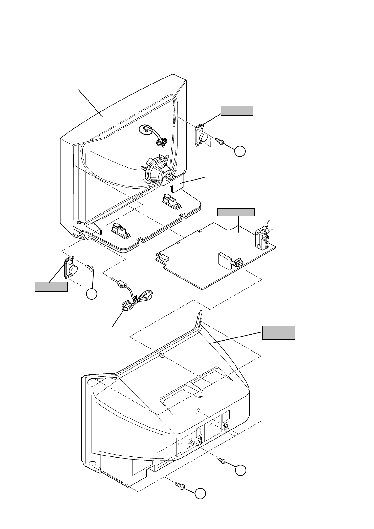
DISASSEMBLY PROCEDURE
REMOVING THE REAR COVER
1. Unp lug the po wer pl u g.
####
!!!!
.
an d a
2. As s h own i n f igur e , remove t he 6 screws marked
screw marked "
3. Wi thdr a w t he r ear c o ver to wa rd you .
".
""
REMOVING THE MAIN PW BOARD
" After removing the rear cover.
1. Sli ght ly r ai se t he both si d es of t he MAIN PW BOARD b y ha nd .
2. Wi thdr a w t he M AIN PW B OARD b ackw ar d.
(If necess ar y, ta k e off the wire c lamp, c onn ect or s etc. )
REMOVING THE SPEAKER
"
After removing the rear cover.
1. As sh own in fi gu re, r em ove th e 2 screws marked
2. Follow th e s ame st eps wh en r em oving th e oth er ha nd sp eak er.
CHECKIN G THE MAIN PW BOARD
1. To ch eck the ba ck s ide of the PW B oar d.
1) Pu ll out the MA IN PW Bo ard. ( Ref er to RE MO VING TH E MAIN
PW B oar d)
2) Er ect th e PW Boar d vert ic al l y so th at you ca n easil y ch eck th e
b ack side of th e PW Boar d.
[CAUTION]
" W hen e re cting th e PW Boar d, be caref ul s o t hat ther e w ill b e n o
con tact in g with ot her PW Boar d.
" Before turning on power, make sure that the CRT earth wire and
oth er co nne cto r ar e p rope rly c onn ect ed.
WIRE CLAMPIN G AND CABLE TYING
1. Be sure to cla mp the wir e.
2. Never r em o v e th e cable ti e use d f or tying th e wires to gethe r.
Sh oul d i t be inad verte ntly r em ove d, be su re to tie th e w ires w it h a
new cable tie.
8
No. 52024
Page 9
A
3
A
A
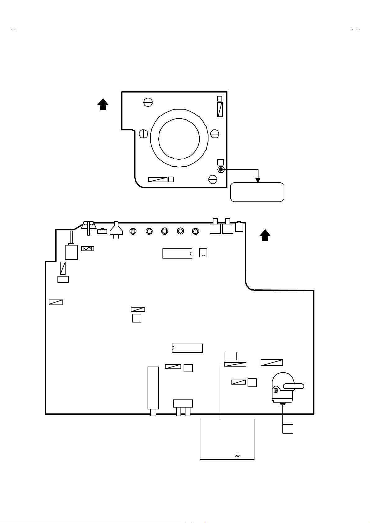
FRONT CABI .
V-21F
V-21FR3
V-21FMG3B
SP EAKER
C
CRT SOCKET
PWB
MAIN PWB
SP EAKER
C
POWER
CORD
REAR
COVER
B
A
No. 52024
9
Page 10
A
V-21F3
A
A
S
U
/C
QSS
OLU
OS
V-21FR3
V-21FMG3B
REPLACEMENT OF MEMORY ICs
1. MEMORY ICs
Thi s mod el u ses me mo r y I Cs. This memo r y IC da ta are f or pr o per opera tion of th e vide o a nd defl ect io n cir cuits.
When r ep la cing memory ICs , b e su r e to use ICs w r it ten w i th t he ini tial v a lu es of dat a.
2. PROCEDURE FOR REPLACIN G MEMORY ICs
(1) Power off
Switch the p ower of f and di sc o nn ect t he pow e r plu g f rom t he w al l out let.
(2) Replace ICs
Be sure to use memory ICs written with the initial data values.
(3) Power on
Connect th e pow er plu g i nt o the wal l ou tl et and s w itch t he po we r on .
(4) C heck and s et SY STEM CONSTAN T SET
・・・・ It must not adjust without adjustment signals.
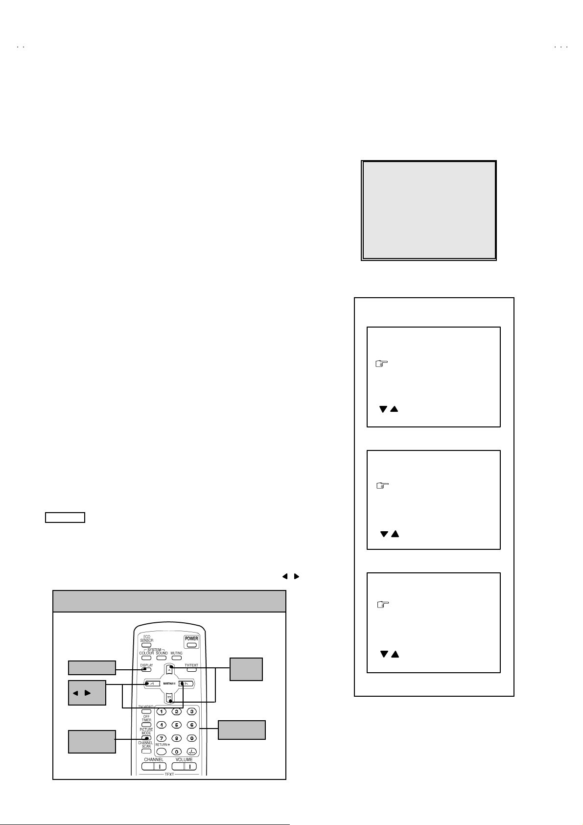
1) Press th e DI SPLAY key and the PICTURE MODE key of the REMOTE
CONTROL UNIT simultaneously.
2) The SERVICE MENU screen of Fig. 1 will be displayed.
3) W hi le th e SE RV ICE MEN U is d is play ed , ag ain p r ess the DISPL AY key and
PICTURE MODE key simultaneously, and the SYSTEM CONSTANT SET
screen of Fig. 2 w ill b e di splayed.
4) Check th e s ettin g value s of the S YSTE M CON ST AN T S ET of T able 1 If th e
val u e is diffe re nt, sel ect the sett i ng it em wi th the MENU ▼/▲key, and set
th e co rrect valu e with t he MENU - / + k ey.
5) Press the DI SPLAY ke y twice, and r etu rn to th e n or m al scr ee n.
(5) Receive channel of setting
Refe r to th e OPE RATING INST RUCTIONS and set th e r ece i ve c ha nn el s
(chan nels prese t) as descr i be d
(6) User Setting
Check t he us er s ettin g valu e of Tab le 2, a nd if se tti ng value is di f feren t, s et
th e co rrect valu e.
For setting , refer to the OPE RATING INSTRUCTIO NS.
(7) Setting of SERVICE MENU
Ve rif y the s et ting it ems of th e SER VICE MENU, and r eset whe r e n ecess a r y.
For setting , refer to the SERVICE ADJUSTMENTS.
NOTE
Alth ou gh th e k ey p osi tion of t he RM-C90 r e mote control unit is diff erent fr o m
th at of t he RM -C36 4GY & R M -C3 64 remot e co ntrol unit, the fu nctio ns of bo th
un its are th e same S o pl eas e us e th e at tach ed diagr a m for th e RM-C90
remote control unit for the RM -C36 4GY & RM-C364.
By t he way, MENU -/+ Key fu nction s in t he sam e ma nner as for / key.
KEY ASSIGNMENT OF REMOTE CONTROL UNIT
ERVICE MEN
1.IF 2.V
3.DEF 4.VSM PRESET
5.PRESET
6.SETUP TOUR OFF
1-6 SELECT DISP : EXIT
******
****** *****
***** **
************
**********
*** ** **
*** ** ** ** ***
*** ** ***** ** **
**.***
****
** ***
** ***** ***
***
******
Fig.1
SY STEM C ON STA NT- ⅠⅠⅠⅠ
SYSTEM CONSTA NT SE T 1
COL O UR :
BILIN GUAL : N O
TUNE R : MU
ECO SENSOR : YES
LANG U AG E :
: SELECT
/
- / + : OPERATE DISP : EXIT
***
***
SY STEM C ON STA NT-
SYSTEM CONSTA NT SE T 2
B/B SO UND : O F F
LOCK : 180
COL OUR AU TO : NO
ALC : NO
TEXT R ATE : 2 0
: SELECT
/
- / + : OPERATE DISP : EXIT
: MINT
SY STEM C ON STA NT- ⅢⅢⅢⅢ
SYSTEM CONSTANT SET 3
AMP T UNER : NO
VNR : YES
TEXT TABLE : CYL
M PWM : P
V
ⅡⅡⅡⅡ
: SELECT
/
- / + : OPERATE DISP : EXIT
DI SPL A Y k ey
MENU
/ key
MENU
▼/▲
key
Fig.2
NUMBERS
PICTURE
MO DE k e y
key
(RM-C90)
10
No. 52024
Page 11
A
3
A
A
SE TT ING OF SY STEM C ON STANT SET
Setting item Setting contents
COLOUR
BILINGUAL
TUNER
AI ECO S ENSOR
LA NG UA G E
B/B SOU ND
LO CK
COLOUR AUTO
QSS
ALC
MUL TI . PA LTRIPLE
YE S NO
MU MA
YE S NO
E/R/A /P E/R
ON OFF
YES 10 20 ~ 230
250 240
YE S NO
MI NT MQ SS
YE S NO
V-21FMG3B
AV-21F3 AV-21FR3 AV-21FMG3B
TRIPLE. MULTI
NO
MU
YE S
E/R
OFF
18 0
NO
MI NT
NO
Setting value
E/R/A /P
V-21F
V-21FR3
TEXT RAT E
AMP TUNER
VNR
TEXT TABLE
VOL UM PW M
USER SE T TING V ALUES
Setting item Setting value Setting item Setting value
SUB POWER ON LANGUAGE ENGLISH
CHA NNEL PO SITIO N 1 PO SITIO N CHA NNEL P RE SET Refe r t o OPE RATIN G I NS TRUCTION
VOL UME About 10 AI ECO S EN SOR OFF
TV/V IDEO
ON SCR EEN DI SPLAY
COLOUR SYSTEM PAL ON TIMER PR1 0:00
SOUND SYSTEM B / G BLUE BACK OFF
OFF TIMER OFF OSD.Shows 00 CHI LD LO CK OFF
PICTURE MODE (VSM) BRIGHT
10 20 40 80
YE S
YE S NO
ARA CYL
POS NEG
NO
TV VNR OFF
POSITION INDICATION AUTO SHUTOFF OFF
20
NO
YE S
CYL
POS
Table 1
Table 2
No. 52024
11
Page 12
A
V-21F3
A
A
)
V-21FR3
V-21FMG3B
INITIAL SETTING VALUE OF SERVICE MENU
1. Ad justmen t of t he SE RVICE MENU is m ad e o n th e bas is o f the initial setti ng va lues ; howev er, the new setting va lues w hich
set the screen in its optimum condition may differ from the initial setting.
2. Do not change the initial Setting Values of the Setting (Adjustment) items not listed In “ADJUSTMENT”.
2. V/C
Initial set ting v al ue
Setting item
2. DRI VE
3. BR IG HT
Colour sy stem
RED
GREE N1. CUT OFF
BL UE
RED
BL UE
Variabl e
range
-128 ~+127
-128 ~+127
-127~+127
PA L SE CAM NT SC 3.5 8 NT SC 4.4 3
-50
+ 0
+ 0
4. CONT .
5. COLOUR -63~+63 + 0
TV
AV -21F3
6. TINT
7. SECAM BL ADJ.
8. SHARP
3. DEFL ECTION
1. VER. POS ITION
2. HOR. POSITION -16 ~ +15 +1 + 4
3. VER. HEIGHT - 64 ~ +63 -40 + 0
4. VE R . L I NE ARIT Y -32 ~ +31 +13 - 3
5. VER. S WCURVE - 32 ~ +31 -32 + 0
6. H OR. VC O AD J UST
VI DEO
Do Not Ad j.
Setting item Variable range
AV -21FR3
AV -2 1FMG3B
TV - 8(Fixed
VI DEO
Do Not Ad j.
-63 ~+63
-63 ~+63
-31 ~+31
-32~+31
-04 ~ +03
-63 ~ +62 + 0 + 0
+ 0
+ 0 + 0
+0 + 0
+8 + 0
+ 0
+15(Fi x ed )
Initial set ting v al ue
fv : 50Hz MODE fv : 60Hz MODE
- 2 - 3
4. VS M PRESE T
12
VS M pr eset
VSM mode
Setting item
TINT SETTING VA LUE +1 5
COLOUR SE TTIN G VA LU E +15
BR IG HT SET TING VA LUE +1 5
CONT . SE TTING VA LUE +30 +15 + 11
SHARP SE TT IN G VA LU E +1 5 +1 2
BRIGHT STANDARD SOFT
No. 52024
Page 13
A
3
A
A
5. PRESE T
The items in the following table, it i s no requirement for adjustment.
If va lues had changed by t he miss operation, se t the initial settin g v alue s i n the following table.
Colour Sy stem Do Not Ad j u st
V-21F
V-21FR3
V-21FMG3B
Setting item
1. C TRAP FIX 1 1 1 1
2. SHARP PEAK 0 0 0 0
3. A BL 1 1 1 1
4. GAMMA 0 0 0 0
TV 0 2 2 3
5. Y. DE LAY TIME
VI DEO 0 2 0 2
6. BLACK EX P START
TV 1 1 0 0
7. C-BPF
VI DEO 1 1 1 1
8. CW / SC P 0 0 0 0
9. VIF DET L EVEL 0 0 0 0
11. IF AGC MIN 0 0 0 0
12 . VIF AGC 0 0 0 0
13. VIF PM OD 0 0 0 0
19 . VN R 15 15 15 15
PA L SE CAM NT SC 3.5 8 NT SC 4.4 3
+3 +3 +3 +3
Initial set ting v al ue ( Fixed value)
20 . R GB LIM 1 1 1 1
21. RGB LIMIT LEVEL 2 2 2 2
23. TEXT H. POSITION -3 -3 -3 -3
24. READ DATA
Sound System D o Not Ad j u s t
Setting item B/G I D/ K M
10. SIF DET L EVEL +0 +0 +0 +0
14. SIF BP F BW ADJUST
15. SIF TRAP FO ADJUST +0 +0 +0 +0
16. SIF TRAP FO ADJUST 2 +0 +0 +0 +0
17. SIF -TRAP 0 0 0 0
18. SIF -BPF 1 0 0 0
22 . SIF SW 0 1 1 1
+
0
+
0
+
0
+
0
No. 52024
13
Page 14
A
V-21F3
A
A
V-21FR3
V-21FMG3B
REPLACEMENT OF IC301 (IF V/C DECODER)
" For the IC301(IF V/C DECODER) of t his mode l, a ll data are written in the micro-computer. So, wri te the data i n the micro-
computer in accordance with the following procedures before starting adjustment.
PROCEDURES
(1) Tur n the POWE R O F F.
(2) Replace t he IC301 with a n ew o ne.
(3) While pr es sing MENU bu tto n a nd VO L+ bu tto n ON the FRONT CABIN E T simul t aneous ly, t urn th e POW ER O N. When the POW ER is
turn ed ON, th e d at a is w ritten in the m icro-compute r immed iately.
LOCATIONS OF FRONT PANEL BUTTONS AND LAMPS
MENU buttons
1
1 2 3 4 5
CHANNEL -/+butto ns
2
(ME NU -/+b uttons)
VOLUME -/+ buttons
3
(MENU -/+ bu tto ns)
AI ECO sensor
4
REMOTE CONTROL sensor
5
ON TIMER lamp
6
POWER lamp
7
MAIN POW ER button
8
7 8
6
14
No. 52024
Page 15
A
3
A
A
SERVICE ADJUSTMENTS
BEFORE STARTING SERVICE ADJUSTMENT
1. There ar e 2 w ay of adjus ti ng thi s TV: One i s wi th t h e
REMOTE CONTROL UNI T and the other is the conventional
method using adjustment parts and components.
2. The adjustment with the REMOTE CONTROL UNIT is made
on the basis of t he initia l se tting v alue s. The sett ing values
which adjust the screen to its optimum condition may differ
from the initia l s etting v al ues.
3. M ake s ur e th at connect ion is c orrec t l y made t o AC p ower
source.
4. Turn on t he power of th e se t an d eq uipm en t bef or e us e, an d
start t he adju stm en t proc edure s af ter waitin g at least 30 min utes.
5. Unl ess ot herwi se spec if i ed, prep ar e th e mo s t s uita bl e r ec epti o n
or inp ut si gn al for adj ust m ent.
6. Nev er t o uch any ad ju s tment parts, wh i ch ar e no t spe cif ied
in the li st for thi s ad justme nt VRs , tra nsf or ms, c ond e n ser s,
etc.
7. Prep ar ati o n for adj ustm en t
Unless otherwise specified in the adjustment instructions, preset
the following functions with the REMOTE CONTRO L UNIT.
User mode position
PICTURE MODE (VSM) BRIGHT
VNR OFF
TINT / COLOUR / BRIG HT
CONT. / SHARP
BLUE BA CK OFF
OFF TIMER OFF
AI ECO S ENSOR OFF
AUTO S HUT O FF OFF
V-21F
V-21FR3
V-21FMG3B
CENTER
MEASURING INSTRUMENT AND FIXTURES
1. DC voltmeter (or digital voltmeter)
2. Oscilloscope
3. Si gn al g ener at or (P att er n g ener at or) [ PAL / S EC AM / N T S C]
4. Remote control unit
ADJUSTMENT ITEMS
Adjustment it em Ad justment item
B1 POW E R SUPPLY
FOCUS adjustment VSM PRESET setting
IF ci rc uit a djust me nt
V/C (Video / Chroma) circuit adjustment
DEFLECTION c ircuit adjustment
PURITY/ CO NV ER GEN C E adj us tm ent
No. 52024
15
Page 16
A
V-21F3
A
A
3
t
V-21FR3
V-21FMG3B
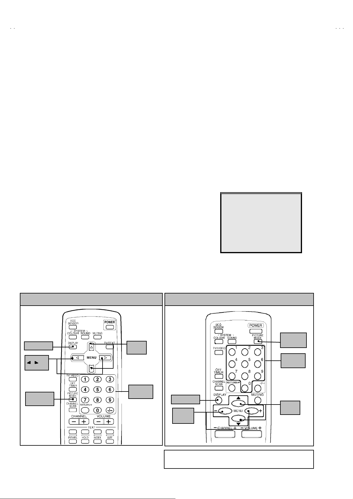
BASIC OPERATION OF SERVICE MENU
"
The adjustment using SERVICE MENU
The f ol lowing adjus tme nt it ems us e t he SE RV IC E M EN U in th e s er ies of the adj u s tm ent . The ad ju stment s are made on the bas is of the
initial s e tting val u es. The ad ju stm ent valu es whic h ad ju st t he s cr een to the o pti m um co ndit io n c an be diffe rent from the i n iti a l sett in g values.
With th e SER VICE ME NU, various s ett in gs c an be made , a nd the y are broa dl y c l ass ifi e d i n the f ollo win g ite ms of s etti n gs.
1.I F ・・・・・・・ ・・・・・・・・・・・・・ ・・・ Ad justment of th e IF cir cuits.
2.V /C ・・・・・・・・・・・・・・・・・・・・・・ Ad ju stm en t of th e VID EO /CHRO MA cir cuit.
3.DEF ・・・・・・・・・・・・・・・・・・・・ ・ Adjustmen t of th e DEFLECTION circuit.
4.V SM PRES ET ・・・・・・・・・・・・ Ad ju stmen t of th e init ia l sett in g va lue s of VSM c o nd it ion as STA NDA RD, SOFT a nd BRIGHT .
(VSM : Video Status Memory)
5.PRESET
6.SETUP TO UR OFF ・・・・・・・ ・ It s hould b e able to selec t m ode (LANGUAG E and AUT O CH PRESE T ).
"
Key operation of the SERVICE MENU
[Enter to SERVICE MENU]
Press the DI SPLAY key and the PICTURE MODE key of the REMOTE CONTROL
UNIT s imult an eou sly. Th en enter the S ERVICE ME N U mod e as sh own in Fig.1 .
[Exit from SERVICE MENU]
When co m plete th e ad j ust me nt wor k , pr ess th e DISPLA Y key to retur n t o th e
SERVICE MENU.
An d th en pr es s the DISPLA Y ke y ag ain, retur n to the n or m al sc r een .
[ Se lec t fr o m SE RV IC E ME NU ]
In SER VI CE M ENU, pr ess t he n umber ( 1 ~6) ke y of th e r emo te c ont ro l un it , to select
an y of th e ad j ustm en t ite ms.
The colours w hi ch se le cte d i te m charact ers a r e ch ang ed .
・・・・・・・ ・・・・・・・・・・
Adjustment of the RF circ uit [Do not adjust].
[Should be OFF].
SE RVICE M EN U
1.IF 2.V/C
.DEF 4.VSM PRESET
5.PRESET
6.SETUP TOUR OFF
1-6 SELECT DISP : EXIT
******
***********
***** **
************
**********
*** ** **
*** ** **** ***
*** ** ***** ** **
**.***
****
** ***
** ***** ***
***
******
Fig.1
KEY ASSIGNMENT OF REMOTE CONTROL UNIT
DI SPL A Y k ey
MENU
/ k ey
PICTURE
MO DE k e y
MENU
key
▼/▲
NUMBERS
key
(RM-C90)
KEY ASSIGNMENT OF REMOTE CONTROL UNIT
PICTURE
MO DE k e y
NUMBERS
key
DI SPL A Y k ey
MENU
MENU
▼/▲ key
-/+key
(RM-C364GY)
(RM-C364)
Exc e pt for diffe re nc e in b ody col o ur , the Remot e Co ntr ol U ni
RM-C 36 4G Y and RM-C3 64 ha ve exac tl y t he s am e Fu nctions.
16
No. 52024
Page 17

A
3
A
A
[Method of setting]
1. IF
[1. VCO]
① 1 K ey ・・・・・・・ ・・・・・・・・・・・・・ ・・・・・ Select 1.IF.
② 1 K ey ・・・・・・・ ・・・・・・・・・・・・・ ・・・・・ Select 1.VCO
③ The VCO (CW) screen will be displayed a allow mark when the AFC voltage is at a certain level.
④ DISPLA Y K ey・・・・・・・ ・・・・・・・・・・・ As you press this key twice, you will return to th e SERVIC E M E NU.
[2. DELA Y P OINT]
① 1 K ey・・・・・・・ ・・・・・・・・・・・・・ ・・・・・ Select 1.IF.
② 2 K ey・・・・・・・ ・・・・・・・・・・・・・ ・・・・・ Se le ct 2.DELAY P OINT.
③ ME NU - /+ K ey ・・・・・・・ ・・・・・・・・・・ Set (adjust) the setting valu es o f th e setting it ems.
④ DISPLAY K ey・・・・・・・・・・・・・・・・・・ W hen th is is presse d twice, you will r et urn t o the SE RVICE MENU .
2.V /C, 3.D EF and 4 .V SM PRES ET
① 2~4Key ・・・・・・・・・・・・・・・・・・・・ ・・・ Select one from 2. V/C, 3. DE F an d 4. VSM PRESET.
② MENU ▼/▲ Key ・・・・・・・・・・・・・・ Se lect setting items.
③ MENU -/+ Key ・・・・・・・・・・・・・・・・・ Adj u st th e va lues of t he i tem s .
④ DISPLA Y K ey ・・・・・・・・・・・・・・・・・・ W hen this is pr esse d, re turn t o t he SE RVICE MEN U.
V-21F
V-21FR3
V-21FMG3B
6.SETUP TOUR
① B y pressing th e 6 key, you can ch ange t he ON or OF F ( should be OFF).
(Should be OFF)
%・
The JVC’s logo will be shown about 15 seconds automatically.
② MENU -/+ K ey ・・・・・・・ ・・・・・・・・・・ Select Language.
③ MENU ▼ Key・・・・・・・・・・・・・・・・・ Au to Se arch.
If it is ON , th en y ou tu rn th e TV po we r off , wh en y ou ar e t urn t he TV p ower o n a gain .
No. 52024
17
Page 18
A
V-21F3
A
A
JUS
6.SETU
ON /
(By p
y)
G
(R)
S
U
O
V-21FR3
V-21FMG3B
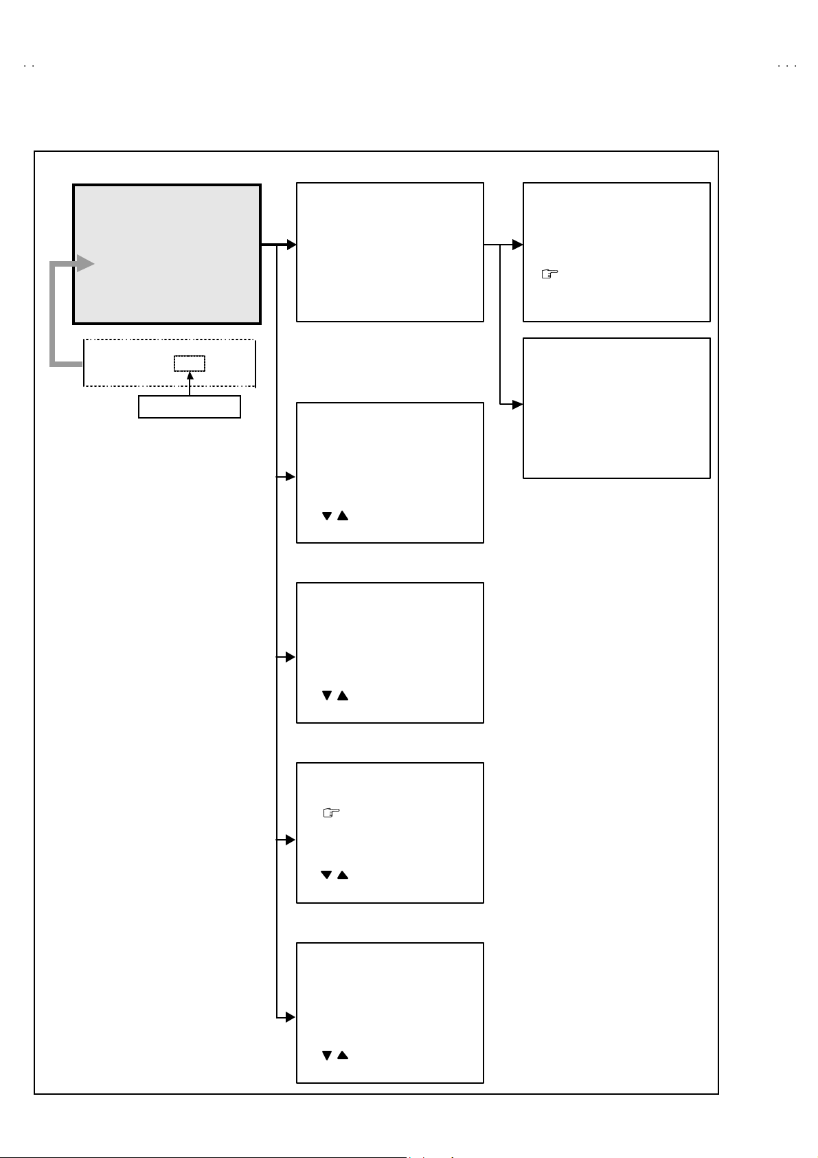
SERVICE MENU FLOW CHART
SE RVICE M EN U
ERVICE MEN
1.IF 2.V/C
3.DEF 4.VSM PRESET
5.PRESET
6.SETUP TOUR OFF
1-6 SELECT DISP : EXIT
******
****** *****
***** **
************
**********
*** ** **
*** ** ** ** ***
*** ** ***** ** **
P TOUR
**.***
****
** ***
** ***** ***
FF
OFF
***
******
ressing 6-ke
SU B ME NU 1. I F
IF
1. VCO
2. DELAY PO INT
1-2 : SELECT DISP : EXIT
SU B ME NU 2. V /C
V/C PAL
1. CUTOFF
50Hz
/ :SELECT
- / + : OPERATE DISP : EXIT
(G)
(B)
* **
* **
* **
VCO (CW)
TOO HIGH
ABOV E REFERENCE
BELOW REF ERENCE
TOO LOW
AFT ADJUST
VCO ADJUST
FINE
DELAY POINT UHF
AGC TAKE- OVER
- / + : OPERATE DISP : EXIT
***.**
T REFERENCE
MH z
** *(* *)
** *(* *)
** *(* *)** *(* *)
** *(* *)
** *(* *)
** *(* *)** *(* *)
DISP : EXIT
**
SU B ME NU 3. D EF
DEF
1. VER. POSITION
50Hz
/ :SELECT
- / + : OPERATE DISP : EXIT
PAL
***
SUB ME NU 4. V SM PR ES ET
BRI GHT
TINT
COLO UR
HT
BRI
CONT.
SHARP
/ :SELECT
- / + : OPERATE DISP : EXIT
**
**
**
**
**
SUB ME NU 5. P RE SET
18
PRESET
1. C -TRAP FI X
50Hz
/ :SELECT
- / + : OPERATE DISP : EXIT
PAL
B/ G
***
No. 52024
Page 19
A
3
A
A
ADJUSTMENT LOCATIONS
V-21F
V-21FR3
V-21FMG3B
TOP
MAIN PWB
F901
CRT SOCKET PWB
TP-47R
TP-47G
T
IC701
(SOLDER SIDE)
U
TP-47B
E1
TP-E
CRT EARTH WIRE
(BRAIDED ASS'Y)
FRONT
IC702
MEMORY IC
DEG
PW
S
TU00 1
IC301
T
1
S
1Pin TP-91(B1)
2Pin NC
3Pin X-ray2
4Pin X-ray1
5Pin TP-E( )
HV
U
HVT
UPPER:FOCUS
LOWER:SCREEN
No. 52024
19
Page 20

A
V-21F3
A
A
)
adjust
V-21FR3
V-21FMG3B
ADJUSTMENTS
B1 POW ER SUPPLY
Item
Check of
B1 Powe r
Measuring
instrume nt
Signal
generator
Supply
DC Vo lt meter
FOCU S ADJUSTMENT
Item
Ad j ust men t
of FOCUS
Measuring
instrume nt
Signal
generator
IF CIRCUIT ADJUS TMENT
Item
Measuring
instrume nt
Test point Adjustment part Description
TP-91 ( B1)
####
TP-E (
)
1. Inp ut a whole blac k s ig na l.
2. Connect a DC voltmeter to TP-91(B1) and TP-E (#).
3. M ake sure t hat the vol t age i s DC1 16.5±2.0 V.
Test point Adjustment part Description
FOCUS VR
[In HVT]
1. Input a cross-hatch signal.
2. W hil e watch ing the scr e en, adjust the FOCUS VR to make the
ver ti cal and ho ri zonta l l ines as f in e a nd sha rp as possi b le.
3. M ake sure t hat whe n the s creen is d arkened, the l i nes rem ain in
g ood focu s.
Test point Adjustment part Description
Ad j ust men t
of VCO(CW
Signal
generator
Remote
control unit
VCO (CW)
TOO HIGH
AB OVE REFEREN CE
JU ST REF ER ENCE
BEL OW R EFERE N CE
TOO LOW
AFT AD JUST
VCO ADJUST
FINE
DISP : EXIT
ADJUSTMENT AT THIS POINT IS USELESS
***.**
MHz
** *(* *)
** *(* *)
** *(* *)** *(* *)
** *(* *)
** *(* *)
** *(* *)** *(* *)
ADJUSTMENT POINT
1. VC O
YE LLOW
Do not
TOO HIGH
ABOVE REFERENCE
J US T R E FE RE NC E
B ELO W RE F E RE NC E
TOO LOW
●Please use signal generator which is correct proof about the
sen ding fr eque nc y.
1. Inp ut th e PA L f ull col o ur b ar (2 10 .2 5MHz) s ig nal .
2. En ter th e SERVICE ME NU.
3. Se lect 1.IF f rom the SERV ICE MENU.
4. Press 1 ke y and s elect 1.VCO.
5. Select VCO ADJUST with MENU ▲/▼ key.
6. Press MENU -/+ key until the colour of t he characters TOO
HIGH ch an ges b lue to ye llow. Then g r ad uall y press th e MEN U
-/+ key u ntil the TOO LOW ch ang es yellow . At thi s t im e, conf irm
th at t he val u e of VCO ADJUST is n ear + 00 .
1. Select AFT ADJUST with MENU ▲/▼ key.
8. Press ME NU -/ + key until the characters JUST REFERENCE
ch ang es bl ue to yellow .
9. Press the DI SPLA Y key three times to return to normal screen.
20
No. 52024
Page 21

A
V-21F
3
A
A
(QAU0287-001)
(QAU0185-004)
(QAU0282-001)
V-21FR3
V-21FMG3B
Item
Ad j ust men t
of DELAY
POI NT
(AGC)
Measuring
instrume nt
Signal
generator
Remote
control unit
DELAY POINT UHF
AGC TA KE-OVER
- / + : OPERATE DISP : EXIT
Test point Adjustment part Description
**
DELAY P OINT
(AGC TAKE-OVER)
1. Inp ut a bl ac k an d wh it e sign al (col o ur of f).
2. En ter th e SERVICE ME NU.
3. Select 1. IF f rom t he SERVI C E M EN U.
4. Select 2 . DELAY P OINT b y pr essi n g the 2 key on the remote
control unit.
5. Se t th e set ting val u es of the s et ting items as s hown bel l o w t able .
6. Then adjust the MENU - or + key until video noise disappears.
7. T ur n to oth er chan nel s and make su r e that the re are n o
irregularities.
Setting It e m Variabl e ra nge Initial se tting v alue
DELAY P OINT
(AGC TAKE OVER)
NT SC 3.5 8
OTHER
0~127
MATSUSHITA
45 45 47
35 45 35
MURATA
ALPS
No. 52024
21
Page 22

A
V-21F3
A
A
(B)
V-21FR3
V-21FMG3B
VIDEO / CHROM A CIRCU IT ADJUSTMENT
The setting (adjustment) using the REMOTE CONTROL UNIT is made on the basis of the initial setting values.
The setting values which adjust the screen to the optimum condition can be different from the initial setting values.
Do no t c hange the init ial setting values of the set ting it ems not list e d in “ADJUSTMENT”.
Item
Ad j ust men t
of WHITE
BALANCE
(Low light)
Measuring
instrume nt
Test point Adjustment part Description
Signal
generator
Remote
control unit
V/C PAL
1. C UTO FF
50Hz
/ :SELECT
- / + : OPERATE DISP : EXIT
(R)
(G)
(B)
* **
* **
* **
KEY ASSIGNMENT OF REMOTE CONTROL UNIT
CU TO FF O F F
(H.LINE OFF)
CU TO FF O N
(H.LINE ON)
R. CUTOFF( )
R. CUTOFF( )
▲
▲
R. DRI VE( )
▼
R. DRI VE( )
▼
123
4
7
56
8
9
RGB
1. CUT OFF (R)
CUT OFF (G)
CUT OFF (B)
SCREEN VR
[IN HVT]
G .C UTOFF ( )
B. C UTO FF( )
B. D RIV E( )
B. C UTO FF( )
B. D RIV E( )
G .C UTOFF ( )
▲
▲
▲
▲
▲
▲
1. Inp ut a bl ac k an d wh it e sign al (col o ur of f).
2. En ter th e SERVICE ME NU.
3. S elect 2. V/C fr om th e S ERVICE MENU, then selec t 1. CUT OFF
(R), (G) and (B) .
4. Set each value to initial setting value with 4~ 9 keys of the
remote control unit.
5. Press the 1 key of the remote co ntr ol un i t to sh ow the sin gl e
horizontal line on screen.
6. T ur n t he SCREEN VR fully counter-clockwise, then slowly turn it
cl ockw is e to where on e of a red , blu e or gre en co lour is fai nt ly
vis ible.
7. Use keys 4~9 of th e r em ote c ontro l unit an d ad ju s t the oth er 2
col o ur s which e x cept th e ap pea r ed c olo ur to whe re the si n gl e
h oriz o nt al lin e app ears whit e.
8. Turn the SCREEN VR to wher e t he si n gl e h or iz ont al line g lows
fain tly.
9. Press the 2 ke y to turn of f the sin gle horizon tal l ine.
10. Press the DISPL AY key t wice to retu rn to the nor mal scr een.
Adjustment it em
R
G
Variabl e
range
-128 ~+127
-128 ~+127
Initial set ting
value
-50
-501. CUT OFF
B -128~+127 -50
Ad j ust men t
of WHITE
BALANCE
(Hi gh light)
Signal
generator
Remote
control unit
2. DRI VE (R
DRI VE ( B)
)
1. Inp ut a bl ac k an d wh it e sign al (col o ur of f).
2. En ter th e SERVICE ME NU.
3. S elect 2. V/C fr om th e S ERVICE MENU.
4. Select 2. DRIVE (R) / (B) with MENU ▼/▲ key, and set each
val u e to ini tial setti ng valu e with 4 a nd 7 or 6 an d 9 keys of th e
remote control unit.
5. Use the keys 4 and 7 or 6 and 9 t o p ro duc e a white scr een
V/C PAL
* **
2. D RIV E
50Hz
/ :SELECT
- / + : OPERATE DISP : EXIT
(R)
* **
22
6. Press the DISPLAY key t wice to retu rn to the nomal screen.
Adjustment it em
Variabl e
range
R - 128~+127 +0
2. DRIVE
B
-128 ~+127
No. 52024
Initial set ting
value
+0
Page 23

A
V-21F
3
A
A
V-21FR3
V-21FMG3B
Item
Ad j ust men t
of
SUB BRI GHT
Ad j ust men t
of
SUB CONT.
Ad j ust men t
of
SUB
COLOUR ⅠⅠⅠⅠ
Measuring
instrume nt
Remote
control unit
Remote
control unit
Remote
control unit
Test point Adjustment part Description
3. BR IG HT 1. R eceiv e an y broadc ast.
2. En ter th e SERVICE ME NU.
3. Select 2. V/C f rom S ERVICE MENU.
4. Select 3. BRIGHT with the MENU ▼/ ▲key.
5. Set the initial setting value with the MENU - / + key.
6. If the brightness is not the best with the initial set value, make
fine adjustment until you get the best brightness.
4. CONT . 1. R eceiv e an y bro adc ast.
2. En ter th e SERVICE ME NU.
3. Select 2. V/C f rom S ERVICE MENU.
1. Select 4. CONT. with the MENU ▼/▲key.
5. Set the initial setting value with the MENU - / + key.
6. If the co ntrast is not t he best with the initial s et value, mak e f ine
adjustment until you get the best contrast .
5. COLOUR [Method of adjustm ent without measuring instrument]
PAL COLOUR
1. R eceiv e a PAL broadc ast.
2. En ter th e SERVICE ME NU.
3. Select 2. V/C f rom t he SERVI C E M EN U.
4. Select 5. COLOUR with the MENU ▼/▲ key.
5. Se t th e initia l setting value for PAL COLO UR with the MENU
- / + key.
6. If t he co l our is no t th e be st w i th th e in itia l s et val u e, mak e fine
adjustment until you get the best colour.
SECAM COLOUR
NTSC 3.58 COLOUR
NTSC 4.43 COLOUR
1. R eceiv e a SECAM b roadc ast.
2. M ake fi ne adju stmen t of SE CA M CO LOU R as previ ou sly .
1. R eceiv e a NTS C 3.5 8MHz br oadca st.
2. M ake si m ilar fin e ad ju stm ent of NTSC 3.58 CO LOU R as
previ ously .
When NTSC 3.58 adjustment completed, NTSC 4.43 will be
automatically set at t he resp ective values.
No. 52024
23
Page 24

A
V-21F3
A
A
))
g
V-21FR3
V-21FMG3B
Item
Ad j ust men t
of SUB
COLOUR
ⅡⅡⅡⅡ
W
Measuring
instrume nt
Signal
generator
Oscillosc ope
Remote
control unit
Y
Cy
Test point Adjustment part Description
TP-47G/R
TP-E (####)
[CRT S OCKET
PWB]
M
5. COLOUR [Method of adjustm ent using measur ing instrument]
R
(A)
PAL COLOUR
B
(-)
0V
(+)
1. Inp ut a PA L full fiel d colou r bar signal (7 5% w h it e).
2. En ter th e SERVICE ME NU.
3. Select 2. V/C f rom S ERVICE MENU.
4. Select 5. COLOUR with the MENU ▼/▲ key.
5. Set the initial setting value of PAL COLOUR with the MENU
- / + key.
6. C on nec t the os c illosc ope be tw ee n TP -4 7G /R a nd T P- E (#).
7. Ad just PAL COL OU R to br i ng th e valu e o f (A) in the illu stration
to + 12V (W - G). ( Volt age value b et we en (W) an d ( G))
G
SECAM CO LOUR
1. Input a SECAM full field colour bar signal (75% white).
2. Set the initial setting value of SECAM COLOUR with the MENU
- / + key.
3. Ad just SE CAM CO LOUR to b rin g th e v al u e of
illu str ation t o +8V(W-G). (Voltage va lue b etween (W) an d ( G ))
(A)
in the
NTSC 3.58 COLOUR
NTSC 4.43 COLOUR
24
1. Inp ut a N TSC 3. 58 full fi e ld colo ur b ar si gn al ( 75 % whi te).
2. Set the initial setting value of NTSC 3.58 COLOUR with the
MENU - / + key.
3. Ad just N TSC 3.5 8 C OL OUR to bri ng t he valu e of (A) in t h e
illu str ati on to + 11V(W-G). (Voltage value between (W) a nd (G
When N TSC 3.5 8 i s set, NT SC 4. 43 will be automatica ll y s e t at t he
resp ec ti ve val ues .
No. 52024
Page 25

A
V-21F
3
A
A
y
g
(B)
V-21FR3
V-21FMG3B
Item
Ad j ust men t
of TINTⅠⅠⅠⅠ
Ad j ust men t
of TINTⅡⅡⅡⅡ
Measuring
instrume nt
Signal
generator
Remote
control unit
Signal
generator
Oscillosc ope
Remote
control unit
Test point Adjustment part Description
6. TINT [Method of adjustment without measuring instrument]
TP-47G/R
TP-E (####)
[CRT
SOCKET
PWB]
NTSC 3.58 T INT
NTSC 4.43 TINT
6. TINT [Method of adjustment using measuring instrument]
NTSC 3.58 T INT
1. Inp ut a N TSC 3. 58 full fi e ld colo ur b ar s igna l (75% white) .
2. En ter th e SERVICE ME NU.
3. Select 2. V/C f rom S ERVICE MENU.
4. Select 6. TINT with t he ME NU ▼/▲ key.
5. Set the initial setting value of NTSC 3.58 with the MENU - / +
key.
6. If you c a nn ot get th e best tin t wi th the in iti al s ettin g va lue, ma ke
fine adjustment until you get the best tint.
When N TSC 3.5 8 i s set, NT SC 4. 43 will be automatica ll y s e t at t he
resp ec ti ve val ues .
1. Inp ut a NTS C 3.5 8 f ull fi el d colo ur bar signal (75% white).
2. En ter th e SERVICE ME NU.
3. Select 2. V/C f rom S ERVICE MENU.
4. Select 6. TINT with t he ME NU ▼/▲ key.
5. Set the initial setting value of NTSC 3.58 with the MENU - / +
key.
6. C on nec t the os c illosc ope be tw ee n TP -4 7G /R a nd T P- E. (#).
7. Adjust NTSC 3.58 TINT to bring the value of (B) in the
illustration +9V(W- Cy). ( Volta ge value be tw ee n (W) and (Cy))
W
B
R
M
(-)
0V
Y
C
G
(+)
NTSC 4.43 TINT
When N TSC 3.5 8 i s set, NT SC 4. 43 will be automatica ll y s e t at t he
resp ec ti ve val ues .
No. 52024
25
Page 26

A
V-21F3
A
A
V-21FR3
V-21FMG3B
Item
of SECAM
BL AC K
OFF SET
KEY ASSIGNMENT OF REMOTE CONTROL UNIT
COLOUR
ON
COLOUR
OFF
Measuring
instrume nt
Remote
control unit
Signal
generator
12 3
Test point Adjustment part Description
7.SECAM
BL ADJUST
[Method of adjustment using measur ing instrument]Ad j ust men t
1. Inp ut a SE CAM fu ll f i el d c olour b ar sign al.
2. En ter th e SERVICE ME NU.
3. Select 2. V/C f rom S ERVICE MENU.
4. Select 7. SECAM BL ADJUST with MENU ▼/▲ key.
5. Set the initial setting value with the MENU - / + key.
6. Switch the ①ke y (c ol ou r OF F ) an d ②key (c ol ou r ON ) on the
remote contr ol an d ma ke sur e th at th er e is no col o ur on th e
blac k an d w h it e scr ee n.
7. If t he bla ck an d whit e scr ee n i s no t b est with th e init ia l sett in g
value, make fine adjustment until you g et the best black and
white screen .
8. W hi l e w atch ing th e s cr e en, adj us t th e v alu e t o be th e s ame
col o ur b etween O N & OFF b y t en key on t he remote c ontr o l
un it.
9. Press the DISPLAY key t wice to retu rn to the normal screen.
4
7
56
8
9
26
No. 52024
Page 27

A
3
A
A
DEFLECTION CIRCUIT ADJUSTMENT
"
The re ar e 2 m od es of adju stm ent (s ettin g value) ---- -- ① 50 Hz m od e and ② 6 0Hz m od e ----- de pe ndi n g upo n th e kind of s igna ls
(ver tic al freq uenc y 5 0Hz / 60Hz) .
"
When ad j uste d i n mod e ① , mode ② will be automatically set.
The setting (adjustmen t) usin g the REMOTE CONTROL UNIT is made on the basis of the initial setting values.
The setting values which adjust the screen to the opti mum condition can be different fr om the initial settin g values.
V-21F
V-21FR3
V-21FMG3B
Item
Ad j ust men t
of V.HEIG HT
&
V. POSIT I ON
Screen
size
92%
Measuring
instrume nt
Test point Adjustment part Description
Signal
generator
Remote
control unit
SU B ME NU 3. D EF
DEF
1. VER. POSITION
50Hz
/ :SELECT
- / + : OPERATE DISP : EXIT
Scre en size
1. VE R. POSITION
3. VE R. HE I G HT
PAL
***
Picture
size
10 0%
1. Inp ut a circle p att ern signal.
2. En ter th e SERVICE ME NU.
3. Select 3. DEF. f rom S ERVIC E MENU.
4. Select 1. VER. POS ITION with the MENU ▼/▲ key.
5. Set the initial setting value with the MENU - / + key.
6. Adjust V and V’ to be equal with the MENU - / + key as sh own in
Fig.2.
7. Inp ut a cr os s -hatc h s ign al.
8. Select 3. V. HEIG HT with the MENU ▼/▲ key.
9. Set the initial setting value with the MENU - / + key.
10. As shown in Fig.1, adjust V E R. HE IGH T and m ake th e vertical
screen size 92% of the pi ctu r e siz e with t he MEN U - / + keys of
remote control unit.
Ad j ust men t
of HOR .
POSITION
Pic ture size 1 00%
Fig.1
Signal
2.HOR. POSIT ION 11. Inp ut a circle p attern si gnal.
generator
Remote
control unit
HH"
V
V'
Fig.2
No. 52024
12. Sele ct 2. HOR POSITION with the MENU ▼/▲ key.
13 . Se t th e initi a l sett i ng value of 2. HOR. POSITION with the
MENU - / + key.
14. Adju st 2. HOR. POSITION to make H= H " as sh own in Fi g. 2
with the MENU - / + ke y.
27
Page 28

A
V-21F3
A
A
V-21FR3
V-21FMG3B
Item
Ad j ust men t
of VER. LI N.
& VER .
SCURVE
Measuring
instrume nt
Signal
generator
Remote
control unit
Fig .3
Test point Adjustment part Description
4. VER. L IN.
5. VER. S CURV E
TOP
CEN TER
BOTTOM
●●●● Whe n the vert ic al lin ea rit y has bee n deteriorated
remark ably, perform the followi ng steps .
15 . Input a cross -hatch sign al.
16. Sele ct 4. VER. LIN. with the MENU ▼/▲ key.
17. Set the initial setting value of 4. VER LIN. with the MENU - / +
key.
18. Sele ct 5. VER. SCURVE with the MENU ▼/▲ key.
19. Set the initial setting value of 5. VER. SCURVE wit h t h e ME NU
- / + key.
20. Adju st 4. VER. LIN. and 5. VER. SCURVE so t hat th e sp ace s
of each lin e as sh own i n F i g. 3 o n TOP, CENTER and
BOTTOM become uniform.
Make su r e th at th e a dj us t me nt is pr o per l y do ne on t he scre en of
60 Hz mode .
[NOTE]
"
Adjust to make both 50Hz & 60Hz are the same v. size and
fine straight line.
"
When ad j ust aga in, adju st 5 0H z m ode fi r s t.
"
When adjust in 60Hz mode, only 60Hz mode is adjust.
VSM PRESET SETTING
Item
Setting of
VS M
PRES ET
Measuring
instrume nt
Remote
control unit
TINT
COLO UR
BRI GHT
CONT.
SHARP
/ :SELECT
- / + : OPERATE DISP : EXIT
Test point Adjustment part Description
TINT
COLOUR
BR IG HT
CONT .
SHARP
1. En ter th e SERVICE ME NU.
2. Select 4. VS M PRESE T from the SERVICE MENU.
3. Se lect BRIG HT with th e P ICTURE MODE ke y.
4. Ad just t he MENU ▼/▲ an d M ENU - / + ke y to b ring the s et
val u es of TI NT
tabl e.
5. R esp ectively select th e VSM PR ES ET mode f or SOFT and
STANDARD, and make similar adjustment as in 3 a bove.
~~~~
SHARP to the values shown in the below
•••• VSM PRESET
BRI GHT
**
**
**
**
**
VS M
Setti ng It em
TINT +15
COLOUR +15
BRIGHT + 15
CONT +30 +15 +11
SHAR P +15
BRIGHT STA NDARD SOFT
←
←
←←
←←
←
+12
28
No. 52024
Page 29

A
3
A
A
PURITY / CONVERGENCE ADJUSTMENT
PURITY ADJUST MENT
1. Dem ag ne tize CR T wit h t he dem a gnetiz er .
V-21F
V-21FR3
V-21FMG3B
2. Loos e n th e re tain er scr ew of the d efl ec tion yok e .
3. Remove th e wed ge s.
4. Inp ut a g r een rast er si gn al fr om the signal ge ner at or , an d tur n
th e scr e en to g r een r aste r.
5. Move the deflection yoke backward.
6. Bring t he l o ng l ug of th e p ur i ty m agn ets on the sho rt lu g a nd
p osit ion t hem hor i zon tal ly. (Fi g. 2)
7. Adju s t t he ga p be tween two l ug s so that th e GREEN RAS TER
will come into the center of the screen. (Fig.3)
8. M ove the d eflect ion y oke for ward, and fix th e pos iti o n of th e
deflection yoke so that the whole screen will bec ome green.
9. Ins ert the w e dge t o th e t op side of the def lect io n yo ke s o that it
will not move.
CR T
#
WEDGE
DEFLECTION
YOKE
P
46
P / C
MAGNET S
P/ C MA GN ETS
P : PURITY M AGN E T
4 : 4 P OLES ( con vergence m agn ets)
6 : 6 P OLES (con v er gen ce magn ets )
Fig.1
PURITY MAG NETS
10 . Inp ut a cross hat ch sig nal.
11 . Ve rif y tha t th e scr e en is horiz on tal.
12 . Inp ut red and bl ue r ast er sign als , a nd m ak e sure tha t purity i s
prop er ly ad juste d.
Long lug
Short lug
(FRO NT VIEW )
Bring the long lug over the short lug
and position them horizontally.
Fig.2
GREEN RASTER
CEN TER
Fig.3
No. 52024
29
Page 30

A
V-21F3
A
A
V-21FR3
V-21FMG3B
STATIC CONVERGENCE ADJUSTMENT
1. Input a cross hat ch si g na l.
2. Using 4 - po le conver ge nce m agn ets , ove rla p t he re d and bl u e
lines in th e c en ter of th e scr een (Fi g. 1) and tu rn the m to
mag ent a (r ed/ blue ).
3. U sing 6 - pol e con ver ge nc e ma gn ets , overlap the
mag ent a( re d/b lue) a nd g r een li nes in t he c en ter of the screen
an d t urn t hem t o whit e.
4. Rep eat 2 and 3 ab ove, an d ma ke b est c onve rge nce.
DYNAMIC C ONVERGENCE ADJUSTMENT
1. Mov e th e def lec tion yok e up an d down and o verlap th e lines in
the periphery. (Fig . 2 )
2. Move th e defl ec ti on yoke left to righ t and over lap t he l in es in the
p erip hery. (Fig. 3)
3. Rep eat 1 and 2 ab ove, an d ma ke b est c onve rge nce.
(FRO NT VIEW )
(FRO NT VIEW )
BLUE
GREEN
RED
Fig.1
GREEN
BLUERED
RED
GREEN
BLUE
●
After ad justm ent, f ix the wedge at the original p osition.
Fas t en the retainer screw of th e def lecti on yoke .
Fi x the 6 magn ets with g lue.
(FRO NT VIEW )
GREEN
RED
BLUE
GREEN REDBLUE
Fig.2
Fig.3
BLUE
GREEN
RED
RED
GREEN
BLUE
BLUE
GREEN
RED
30
No.52024
Page 31

A
3
A
A
REPLACEMENT OF CHIP COMPONENT
!
CAUT IONS
1. Avoid heating for more than 3 seconds.
2. Do not ru b t he elec t ro des an d t he r esist p arts of the p att ern.
3. When r em oving a c hip par t, mel t th e s older adequ atel y .
4. Do not r eus e a ch ip p ar t afte r re movi ng it .
! SOLDERING IRON
1. Use a hi g h ins ulati o n s older ing i r on with a t hin po in ted end of it .
2. A 3 0 w s older i ng i r on is r ecommend ed for easily r em oving par ts.
! REPLACEMENT STEPS
1. How to remove Chip parts
$$$$ Resi st o rs, capacitors , et c
(1) As s h own in t he f ig ur e, push th e pa rt with tw ee zer s and
alte rn at ely m elt th e sol de r at each en d.
(2) Sh if t w i th tweez e rs and r emo ve th e ch i p p ar t.
$$$$ Trans isto rs, dio d es , va ria bl e r esistor s, etc
(1) Ap pl y e xt ra s o ld er to each le ad .
SOLDE R SOLD E R
V-21F
V-21FR3
V-21FMG3B
2. How to install Chip parts
$$$$
Resi st ors, ca pacitors , et c
(1) Apply sold er to the patt ern as ind icated in the fi g ure.
(2) Gr asp t he c h i p p art with tweezer s and pl ac e it on th e s ol d er.
The n hea t and me lt th e so lder a t b oth ends of t he chip part.
$$$$ Tran s ist ors, diodes , varia bl e res ist or s, et c
(1) Apply sold er to the patt ern as ind icated in the fi g ure.
(2) Grasp the ch ip p art wit h t we ez e rs and p lace it on th e so l der .
(3) First s older lead A as indicated i n t he figu re.
A
(2) As s h own in t he f ig ur e, push th e pa rt with tw ee zer s and
alte rn at ely m elt th e sold er a t each le ad. S hi ft an d r em ove t he
chip part.
(4) The n solder le ads B and C.
Note : A fte r re moving t he part , remove r emaining solder fr o m the
pattern.
C
A
C
No.52024
B
B
31
Page 32

A
V-21F3
A
A
V-21FR3
V-21FMG3B
32
No.52024
Page 33

A
V-21F
3
A
A
V-21FR3
V-21FMG3B
PARTS LIST
CAUTION
! The parts identifi ed by the ! symbol are i m por t ant for t he safe ty. W hene ver replaci ng the se parts , be s ure t o use s pec if i ed o nes to se cure
the safety .
!
The parts n ot i nd ic ated in th is P arts L ist a nd tho se whic h ar e fil led with lines in the Part s No. columns will not be supplied.
! P. W. Board Ass'y will not be supplied, but those which are filled with the Parts No. in the Parts No. columns will be s upplied.
ABBREVIATIONS OF RESISTOR S, CAPACITORS AND TOLERANCES
RESISTORS CAPACITORS
C R Carbon Resistor C CAP. Ceramic Capacitor
F R Fusible Resistor E CAP. Electrolytic Capacitor
P R Plate Resistor M CAP. Mylar Capacitor
V R Variable Resisto
HV R High Voltage Resistor MF CAP. Metalized Film Capacitor
MF R Metal Film Resistor MM CAP. Metalized Mylar Capacitor
MG R Metal Glazed Resistor MP CAP. M etalize d Polystyrol Capacitor
MP R M etal Plate Resis to r PP CA P. Po lyp ropyl en e Ca pa citor
OM R M etal Ox i de F ilm R esistor PS CA P. Polystyrol Capacitor
CMF R Coating Metal Film Resistor TF CAP. Thin Film Capacitor
UNF R Non- F lammable Resi sto r MP P CAP . M etalize d Poly pr op ylene Cap acito r
CH V R Chip Variable Resistor TAN. CAP. Tantalum Capacit or
CH MG R Chip Metal Glazed Resistor CH C CAP. Chip Ceramic Capacitor
COMP . R Com posi tio n Re sist or BP E C AP . Bi- Pol a r E lectroly ti c Capaci t or
LP TC R
Linear P ositive T emperat ur e C o eff ici e nt
Resistor
r
HV CAP. High Voltage Capacitor
CH AL E CAP. Chip Aluminum Electrolytic Capacitor
CH AL BP CAP.
CH TAN. E CAP.
Chip A lum i num B i- Po l ar C ap acitor
Chip T ant alum Elec trol ytic C ap acitor
CH AL BP E C AP.
Chip T ant alum Bi-Po l ar El ectro lytic Ca pac it or
TOLERANCES
FGJ KMNRHZ P
±1% ±2% ±5% ±10 % ±20 % ±30%
+30%
-10%
No. 52024
+50%
-10%
+80%
-20%
+100 %
-0%
33
Page 34

A
V-21F3
A
A
]
V-21FR3
V-21FMG3B
CONTENTS
!
USING PW BOARD & REMOTE CONTROL UNIT
・・・・・・・ ・・・・・・・・・・・・・ ・・・・・・・・・・・・ ・・・・・・・ ・・・・・・・・・・・・・・
34
! REMOTE CONTROL UNIT PART S LIST ・・・・・・・ ・・・・・・・・・・・・・ ・・・・・・・・・・・・ ・・・・・・・・・・・・・・・・・・・・ ・・・・・・・・・・・・ 35
!
EXPLODED VIEW PARTS LIST
!
EXPLODED VIEW
!
PRINTED WIRING BOARD PARTS LIST
・・・・・・・ ・・・・・・・・・・・・・ ・・・・・・・・・・・・ ・・・・・・・ ・・・・・・・・・・・・・・・・・・・・・・・・・ ・・・・・・・ ・・・・・・・・・・・・・ ・・・・
・・・・・・・ ・・・・・・・・・・・・・ ・・・・・・・・・・・・・・・・・・・ ・・・・・・・・・・・・・ ・・・・・・・・・・・・・・・・・・・ ・・・
36
37
[ AV- 21F 3
"
MAIN PW B OARD ASS ' Y (SCG-14 11 A- H2) (W ith CR T SO CKET PW BOAR D) ・・・・・・・ ・・・・・・・・・・・・・・・・・・・・・・・・・ ・・・・・ 38
[ AV-21FR3 ]
" MAIN PW BOAR D AS S' Y (SCG-14 02 A- H2) (Wi th CRT SO CK ET PW BOARD) ・・・・・・・ ・・・・・・・・・・・・・ ・・・・・・・・・・・・ ・・・・・ 42
[ AV-21FMG3B ]
" MAIN PW BOAR D AS S' Y (SCG-14 32 A- H2) (Wi th CRT SO CK ET PW BOARD) ・・・・・・・ ・・・・・・・・・・・・・ ・・・・・・・・・・・・ ・・・・・
!
PACKI NG PA RTS LIST
!
PACKING・・・・・・・ ・・・・・・・・・・・・・・・・・・・・・・・・・・・・・・・・ ・・・・・・・・・・・・・ ・・・・・・・・・・・・ ・・・・・・・・・・・・・・・・・・・・ ・・・・・・・・・・・・・・ 51
・・・・・・・ ・・・・・・・・・・・・・ ・・・・・・・・・・・・・・・・・・・ ・・・・・・・・・・・・・ ・・・・・・・・・・・・・・・・・・・ ・・・・・・・・・・・・
46
50
USING PW BOARD & REMOTE CONTROL UNIT
PW B AS S ' Y
Model
AV-21F3
AV-21FR3 SCG-1402A-H2 RM-C90-1H
AV-21FMG3B SCG -1432A-H2 RM-C364-1H
MAIN PWB REMOTE CONTROL UNIT
SCG-1411A-H2 RM-C364GY-1H
34
No. 52024
Page 35

A
3
A
A
REMOTE CONTROL UNIT PARTS LIST
[ AV-21F3 ] (RM-C364GY-1H)
!
Ref.No. Part No. Part Name. Description
1 25-1168F BATTERY COVER
[ AV-21FR3] (RM-C90-1H)
Ref.No. Part No. Part Name. Description
!
1 25-1168F BATTERY COVER
[ AV-21FMG3B] (RM-C364-1H)
V-21F
V-21FR3
V-21FMG3B
!
Ref.No. Part No. Part Name. Description
1 25-1168F BATTERY COVER
1
No. 52024
35
Page 36

A
V-21F3
A
A
V-21FR3
V-21FMG3B
EXPLODE D VIEW PARTS LIST
!
Ref.No. Part No. Part Name Description
AV -2 1F 3
!
V01 A51KQK99X PICTURE TUBE
!
L01 QQW0077-001 DEG COIL or QQW0076-001
DY01 QQD0061-001 DEF YOKE
!
T1522 QQH0134-001 F B T
!
!
1 L C1 03 94 -0 3 8A -H F RO NT CA BI NE T
2 CM48006-007-C JVC MARK
!
3 LC30617-001C-H E.E.WINDOW
4 LC30616-004A-H POWER KNOB
!
5 CM35235-006-H SPRING
!
6 LC20292-004A-H CONTROL KNOB
!
7 LC30618-001B-H LED LENS
8 A48457-3-H SPRING
9 CHGB0016-0B-FH BRAIDED WIRE
10 A75034-B P C MAGNET or CE42378-00B
11 CE42764-00A WEDGE ASSY (X3)
!
12 CM36623-B01-H CHASSIS RAIL (X2)
13 QAS0036-001 SPEAKER (X2)SP01
14 QMPR340-165-K2 POWER CORD
!
15 CM47005-A01-H CORD CLAMP
!
16 LC10448-002B-H REAR COVER
!
!
17 LC20377-010B-H RATING LABEL
18 QYSBSF3010Z TAP SCREW (X1)For REAR COVER
19 QYSBSFG4016Z TAP SCREW (X6)For REAR COVER
AV -2 1F R3
V01 A51KQK99X PICTURE TUBE
!
!
L01 QQW0077-001 DEG COIL or QQW0076-001
!
DY01 QQD0061-001 DEF YOKE
!
T1522 QQH0134-001 F B T
1 L C1 03 9 4- 03 7A -H F RO NT CA BI NE T
!
2 CM48006-007-C JVC MARK
!
3 LC30617-001C-H E.E.WINDOW
!
4 LC30616-004A-H POWER KNOB
5 CM35235-006-H SPRING
6 LC20292-004A-H CONTROL KNOB
!
7 LC30618-001B-H LED LENS
!
8 A48457-3-H SPRING
9 CHGB0016-0B-FH BRAIDED WIRE
10 A75034-B P C MAGNET or CE42378-00B
11 CE42764-00A WEDGE ASSY (X3)
12 CM36623-B01-H CHASSIS RAIL (X2)
!
13 QAS0036-001 SPEAKER (X2)SP01
!
14 QMPR340-165-K2 POWER CORD
!
15 CM47005-A01-H CORD CLAMP
16 LC10448-002B-H REAR COVER
!
17 LC20377-001B-H RATING LABEL
!
18 QYSBSF3010Z TAP SCREW (X1)For REAR COVER
19 QYSBSFG4016Z TAP SCREW (X6)For REAR COVER
AV-21FMG3B
!
V01 A51KQK99X PICTURE TUBE
!
L01 QQW0077-001 DEG COIL or QQW0076-001
DY01 QQD0061-001 DEF YOKE
!
T1522 QQH0131-001 F B T
!
!
1 L C1 03 9 4- 03 9A -H F RO NT CA BI NE T
2 CM48006-007-C JVC MARK
!
3 LC30617-001C-H E.E.WINDOW
4 LC30616-004A-H POWER KNOB
!
5 CM35235-006-H SPRING
!
6 LC20292-004A-H CONTROL KNOB
!
7 LC30618-001B-H LED LENS
8 A48457-3-H SPRING
9 CHGB0016-0B-FH BRAIDED WIRE
10 A75034-B P C MAGNET or CE42378-00B
11 CE42764-00A WEDGE ASSY (X3)
!
12 CM36623-B01-H CHASSIS RAIL (X2)
13 QAS0036-001 SPEAKER (X2)SP01
14 QMPR340-165-K2 POWER CORD
!
15 CM47005-A01-H CORD CLAMP
!
16 LC10448-002B-H REAR COVER
!
!
17 LC20377-010B-H RATING LABEL
18 QYSBSF3010Z TAP SCREW (X1)For REAR COVER
19 QYSBSFG4016Z TAP SCREW (X6)For REAR COVER
36
No. 52024
Page 37

A
3
A
A
EXPLODE D VIEW
V-21F
V-21FR3
V-21FMG3B
!
L01
!
!
6
1
8
!
7
!
V01
11
9
CRT SOCKET
PWB
!
12
10
13
!
1
MAIN PWB
2
!
3
!
T1522
!
5
4
!
DY 01
13
!
!
12
!
14
15
!
17
!
16
(×6)
19
No. 52024
18
(×1)
37
Page 38

A
V-21F3
PRINTED WIRING BOARD PARTS LIST
[ AV-21F3 ]
MAIN P.W. BOARD ASS’Y (SCG-1411A-H2)
Symbol No. Part No. Part Name Description
!
RESISTOR
R1002 NRSA63J-221X MG R 220Ω 1/16W J
R1003 NRSA63J-221X MG R 220Ω 1/16W J
R1004 NRSA63J-563X MG R 56kΩ 1/16W J
R1102 NRSA63J-750X MG R 75Ω 1/16W J
R1103 NRSA63J-100X MG R 10Ω 1/16W J
R1109 NRSA63J-682X MG R 6.8kΩ 1/16W J
R1110 NRSA63J-272X MG R 2.7kΩ 1/16W J
R1111 NRSA63J-181X MG R 180Ω 1/16W J
R1112 NRSA63J-100X MG R 10Ω 1/16W J
R1113 NRSA63J-101X MG R 100Ω 1/16W J
R1120 NRSA63J-391X MG R 390Ω 1/16W J
R1121 NRSA63J-221X MG R 220Ω 1/16W J
R1159 NRSA02J-184X MG R 180kΩ 1/10W J
R1301 NRSA63J-221X MG R 220Ω 1/16W J
R1302 NRSA63J-472X MG R 4.7kΩ 1/16W J
R1303 NRSA63J-101X MG R 100Ω 1/16W J
R1304 NRSA63J-101X MG R 100Ω 1/16W J
R1305 NRSA63J-101X MG R 100Ω 1/16W J
R1306 NRSA63J-221X MG R 220Ω 1/16W J
R1307 NRSA63J-122X MG R 1.2kΩ 1/16W J
R1308 NRSA63J-182X MG R 1.8kΩ 1/16W J
R1312 NRSA63J-0R0X MG R 0.0Ω 1/16W J
R1313 NRSA63J-102X MG R 1kΩ 1/16W J
R1314 NRSA63J-102X MG R 1kΩ 1/16W J
R1321 NRSA63J-152X MG R 1.5kΩ 1/16W J
R1322 NRSA63J-272X MG R 2.7kΩ 1/16W J
R1323 NRSA63J-103X MG R 10kΩ 1/16W J
R1324 NRSA63J-102X MG R 1kΩ 1/16W J
R1326 NRSA63J-101X MG R 100Ω 1/16W J
R1327 NRSA02J-475X MG R 4.7MΩ 1/10W J
R1341 NRSA63J-332X MG R 3.3kΩ 1/16W J
R1347 NRSA63J-392X MG R 3.9kΩ 1/16W J
R1349 NRSA63J-472X MG R 4.7kΩ 1/16W J
R1351 NRSA63J-151X MG R 150Ω 1/16W J
R1352 NRSA63J-151X MG R 150Ω 1/16W J
R1353 NRSA63J-151X MG R 150Ω 1/16W J
R1354 NRSA63J-331X MG R 330Ω 1/16W J
R1355 NRSA63J-331X MG R 330Ω 1/16W J
R1356 NRSA63J-331X MG R 330Ω 1/16W J
R1357 NRSA63J-101X MG R 100Ω 1/16W J
R1358 NRSA63J-101X MG R 100Ω 1/16W J
R1359 NRSA63J-101X MG R 100Ω 1/16W J
R1360 QRZ0107-152Z C R 1.5kΩ 1/2W K
R1361 QRZ0107-152Z C R 1.5kΩ 1/2W K
R1362 QRZ0107-152Z C R 1.5kΩ 1/2W K
R1363 QRL029J-123 OM R 12kΩ 2W J
R1364 QRL029J-123 OM R 12kΩ 2W J
R1365 QRL029J-123 OM R 12kΩ 2W J
R1366 NRSA63J-182X MG R 1.8kΩ 1/16W J
R1367 NRSA63J-182X MG R 1.8kΩ 1/16W J
R1368 NRSA63J-182X MG R 1.8kΩ 1/16W J
R1372 NRSA63J-0R0X MG R 0.0Ω 1/16W J
R1374 NRSA63J-392X MG R 3.9kΩ 1/16W J
R1401 NRSA63J-103X MG R 10kΩ 1/16W J
R1421 NRSA63J-472X MG R 4.7kΩ 1/16W J
R1423 NRSA63J-0R0X MG R 0.0Ω 1/16W J
R1424 NRSA63J-0R0X MG R 0.0Ω 1/16W J
R1425 NRSA63J-332X MG R 3.3kΩ 1/16W J
R1426 NRSA63J-0R0X MG R 0.0Ω 1/16W J
R1429 NRSA63J-103X MG R 10kΩ 1/16W J
R1430 NRSA63J-823X MG R 82kΩ 1/16W J
R1431 NRSA63J-103X MG R 10kΩ 1/16W J
R1432 QRE121J-3R9Y C R 3.9Ω 1/2W J
R1433 QRE121J-2R7Y C R 2.7Ω 1/2W J
R1436 NRSA63J-823X MG R 82kΩ 1/16W J
R1437 NRSA63J-822X MG R 8.2kΩ 1/16W J
R1438 NRSA63J-223X MG R 22kΩ 1/16W J
R1439 NRSA63J-104X MG R 100kΩ 1/16W J
R1440 QRE121J-471Y C R 470Ω 1/2W J
R1441 NRSA63J-822X MG R 8.2kΩ 1/16W J
R1442 NRSA63J-103X MG R 10kΩ 1/16W J
R1443 QRE121J-1R0Y C R 1.0Ω 1/2W J
Symbol No. Part No. Part Name Description
!
RESISTOR
R1453 NRSA63J-272X MG R 2.7kΩ 1/16W J
R1502 NRSA63J-0R0X MG R 0.0Ω 1/16W J
R1503 NRSA63J-682X MG R 6.8kΩ 1/16W J
R1525 QRL029J-180 OM R 18Ω 2W J
R1526 QRE121J-271Y C R 270Ω 1/2W J
R1529 QRL039J-681 OM R 680Ω 3W J
R1531 NRSA63J-331X MG R 330Ω 1/16W J
R1532 NRSA63J-102X MG R 1kΩ 1/16W J
R1551 QRZ9011-1R0 F R 1.0 Ω 1/2W J
!
R1552 QRJ146J-2R2X C R 2.2Ω 1/4W J
R1554 QRE121J-681Y C R 680Ω 1/2W J
R1571 QRE121J-222Y C R 2.2kΩ 1/2W J
R1573 QRT029J-1R5 MF R 1.5Ω 2W J
R1574 QRT029J-1R5 MF R 1.5Ω 2W J
R1576 QRE121J-223Y C R 22kΩ 1/2W J
R1577 NRSA63J-392X MG R 3.9kΩ 1/16W J
R1578 NRSA63J-103X MG R 10kΩ 1/16W J
R1581 QRE121J-182Y C R 1.8kΩ 1/2W J
R1582 NRSA63J-223X MG R 22kΩ 1/16W J
R1583 NRSA63J-393X MG R 39kΩ 1/16W J
R1651 NRSA63J-472X MG R 4.7kΩ 1/16W J
R1652 NRSA63J-102X MG R 1kΩ 1/16W J
R1653 NRSA63J-331X MG R 330Ω 1/16W J
R1654 NRSA63J-223X MG R 22kΩ 1/16W J
R1655 NRSA63J-473X MG R 47kΩ 1/16W J
R1656 NRSA63J-822X MG R 8.2kΩ 1/16W J
R1657 NRSA63J-222X MG R 2.2kΩ 1/16W J
R1658 NRSA63J-222X MG R 2.2kΩ 1/16W J
R1659 QRE121J-4R7Y C R 4.7Ω 1/2W J
R1660 NRSA63J-153X MG R 15kΩ 1/16W J
R1661 QRE121J-271Y C R 270Ω 1/2W J
R1662 QRE121J-271Y C R 270Ω 1/2W J
R1664 NRSA63J-682X MG R 6.8kΩ 1/16W J
R1665 NRSA63J-103X MG R 10kΩ 1/16W J
R1666 NRSA63J-101X MG R 100Ω 1/16W J
R1667 QRE121J-101Y C R 100Ω 1/2W J
!
R1668 QRT029J-5R6 MF R 5.6Ω 2W J
R1701 NRSA63J-562X MG R 5.6kΩ 1/16W J
R1702 NRSA63J-682X MG R 6.8kΩ 1/16W J
R1703 NRSA63J-392X MG R 3.9kΩ 1/16W J
R1704 NRSA63J-221X MG R 220Ω 1/16W J
R1705 NRSA63J-221X MG R 220Ω 1/16W J
R1706 NRSA63J-561X MG R 560Ω 1/16W J
R1707 NRSA63J-561X MG R 560Ω 1/16W J
R1708 NRSA63J-102X MG R 1kΩ 1/16W J
R1709 NRSA63J-472X MG R 4.7kΩ 1/16W J
R1710 NRSA63J-472X MG R 4.7kΩ 1/16W J
R1711 NRSA63J-472X MG R 4.7kΩ 1/16W J
R1712 NRSA63J-472X MG R 4.7kΩ 1/16W J
R1713 NRSA63J-472X MG R 4.7kΩ 1/16W J
R1714 NRSA63J-472X MG R 4.7kΩ 1/16W J
R1715 NRSA63J-221X MG R 220Ω 1/16W J
R1716 NRSA63J-221X MG R 220Ω 1/16W J
R1718 NRSA63J-561X MG R 560Ω 1/16W J
R1719 NRSA63J-102X MG R 1kΩ 1/16W J
R1720 NRSA63J-472X MG R 4.7kΩ 1/16W J
R1721 NRSA63J-103X MG R 10kΩ 1/16W J
R1723 QRL039J-270 OM R 27Ω 3W J
!
R1725 NRSA63J-102X MG R 1kΩ 1/16W J
R1726 NRSA63J-472X MG R 4.7kΩ 1/16W J
R1727 NRSA63J-153X MG R 15kΩ 1/16W J
R1728 NRSA63J-102X MG R 1kΩ 1/16W J
R1729 NRSA63J-102X MG R 1kΩ 1/16W J
R1730 NRSA63J-103X MG R 10kΩ 1/16W J
R1731 NRSA63J-472X MG R 4.7kΩ 1/16W J
R1736 NRSA63J-823X MG R 82kΩ 1/16W J
R1737 NRSA63J-104X MG R 100kΩ 1/16W J
R1738 NRSA63J-103X MG R 10kΩ 1/16W J
R1739 NRSA63J-103X MG R 10kΩ 1/16W J
R1740 NRSA63J-392X MG R 3.9kΩ 1/16W J
R1741 NRSA63J-561X MG R 560Ω 1/16W J
R1742 NRSA63J-563X MG R 56kΩ 1/16W J
38
No. 52024
Page 39

A
3
[ AV-21F3 ]
V-21F
Symbol No. Part No. Part Name Description
!
RESISTOR
R1746 NRSA63J-103X MG R 10kΩ 1/16W J
R1747 NRSA63J-0R0X MG R 0.0Ω 1/16W J
R1748 NRSA63J-101X MG R 100Ω 1/16W J
R1749 NRSA63J-472X MG R 4.7kΩ 1/16W J
R1771 NRSA63J-821X MG R 820Ω 1/16W J
R1772 NRSA63J-821X MG R 820Ω 1/16W J
R1791 NRSA63J-221X MG R 220Ω 1/16W J
R1792 NRSA63J-221X MG R 220Ω 1/16W J
R1793 NRSA63J-221X MG R 220Ω 1/16W J
R1794 NRSA63J-221X MG R 220Ω 1/16W J
R1795 NRSA63J-221X MG R 220Ω 1/16W J
R1796 NRSA63J-103X MG R 10kΩ 1/16W J
R1797 NRSA63J-153X MG R 15kΩ 1/16W J
R1802 NRSA63J-750X MG R 75Ω 1/16W J
R1806 QRE121J-271Y C R 270Ω 1/2W J
R1807 NRSA63J-680X MG R 68Ω 1/16W J
R1810 QRG01GJ-560 OM R 56Ω 1W J
R1811 NRSA63J-221X MG R 220Ω 1/16W J
R1815 QRE121J-181Y C R 180Ω 1/2W J
R1816 NRSA63J-681X MG R 680Ω 1/16W J
R1817 NRSA63J-472X MG R 4.7kΩ 1/16W J
R1901 QRF104K-3R9 UNF R 3.9Ω 10W K
R1903 QRL029J-104 OM R 100kΩ 2W J
R1904 QRL039J-151 OM R 150Ω 3W J
R1906 QRL029J-104 OM R 100kΩ 2W J
R1921 QRE121J-2R2Y C R 2.2Ω 1/2W J
R1922 QRE121J-221Y C R 220Ω 1/2W J
R1923 QRM034J-R22 M P R 0.22kΩ 3W J
R1928 QRL039J-683 OM R 68kΩ 3W J
R1933 QRE121J-4R7Y C R 4.7Ω 1/2W J
R1934 NRSA63J-683X MG R 68kΩ 1/16W J
R1935 QRE121J-562Y C R 5.6kΩ 1/2W J
R1974 NRSA63J-222X MG R 2.2kΩ 1/16W J
R1976 QRT029J-8R2 MF R 8.2Ω 2W J
R1977 QRE121J-122Y C R 1.2kΩ 1/2W J
R1978 NRSA63J-473X MG R 47kΩ 1/16W J
R1979 QRL039J-220 OM R 22Ω 3W J
R1980 QRL029J-152 OM R 1.5kΩ 2W J
R1991 QRZ9046-825Z C R 8.2MΩ 1/2W K
!
CAPACITOR
C1001 QETN1HM-106Z E CAP. 10µF 50V M
C1002 NCB31HK-103X C CAP. 0.01µF 50V K
C1004 QETN1CM-477Z E CAP. 470µF 16V M
C1005 QFV71HJ-104Z MF CAP. 0.1µF 50V J
C1008 QETN1HM-475Z E CAP. 4.7µF 50V M
C1103 QETN1EM-476Z E CAP. 47µF 25V M
C1104 NCB31HK-472X C CAP. 4700pF 50V K
C1105 NCB31HK-472X C CAP. 4700pF 50V K
C1106 NCB31HK-472X C CAP. 4700pF 50V K
C1107 NCB31HK-472X C CAP. 4700pF 50V K
C1110 NRSA63J-0R0X MG R 0.0Ω 1/16W J
C1112 QETN1EM-476Z E CAP. 47µF 25V M
C1113 NCB31HK-472X C CAP. 4700pF 50V K
C1114 NCB31HK-103X C CAP. 0.01µF 50V K
C1115 NCB31HK-103X C CAP. 0.01µF 50V K
C1116 NCB31HK-103X C CAP. 0.01µF 50V K
C1117 QFV71HJ-224Z MF CAP. 0.22µF 50V J
C1119 QETN1HM-474Z E CAP. 0.47µF 50V M
C1120 NDC31HJ-121X C CAP. 120pF 50V J
C1121 NCB31HK-103X C CAP. 0.01µF 50V K
C1122 NCB31HK-103X C CAP. 0.01µF 50V K
C1162 NCB31HK-152X C CAP. 1500pF 50V K
C1301 NCB31HK-123X C CAP. 0.012 µF 50V K
C1302 QETN1HM-475Z E CAP. 4.7µF 50V M
C1303 NDC31HJ-100X C CAP. 10pF 50V J
C1304 QFV71HJ-474Z MF CAP. 0.47µF 50V J
C1305 QETN1HM-474Z E CAP. 0.47µF 50V M
C1306 NCB31HK-103X C CAP. 0.01µF 50V K
C1307 QETN1CM-477Z E CAP. 470µF 16V M
C1308 QETN1CM-107Z E CAP. 100µF 16V M
C1309 NCB31HK-103X C CAP. 0.01µF 50V K
C1310 NDC31HJ-221X C CAP. 220pF 50V J
C1311 NCB31HK-103X C CAP. 0.01µF 50V K
Symbol No. Part No. Part Name Description
!
CAPACITOR
C1312 QENC1HM-474Z BP E CAP 0.47µF 50V M
C1313 QETN1HM-335Z E CAP 3.3µF 50V M
C1314 NCB31HK-103X C CAP. 0.01µF 50V K
C1315 QETN1CM-107Z E CAP. 100µF 16V M
C1316 QETN1HM-106Z E CAP. 10µF 50V M
C1317 NCB31EK-473X C CAP. 0.047 µF 25V K
C1321 NDC31HJ-120X C CAP. 12pF 50V J
C1322 NCB31EK-273X C CAP. 0.027 µF 25V K
C1323 QETN1HM-474Z E CAP. 0.47µF 50V M
C1324 QETN1HM-106Z E CAP. 10µF 50V M
C1325 QENC1HM-106Z BP E CAP. 10µF 50V M
C1326 NCS21HJ-221X C CAP. 220pF 50V J
C1341 QETN1HM-106Z E CAP. 10µF 50V M
C1352 QFZ0097-103 MM CAP. 0.01µF 1250V K
C1354 NDC31HJ-271X C CAP. 270pF 50V J
C1355 NDC31HJ-221X C CAP. 220pF 50V J
C1356 NDC31HJ-331X C CAP. 330pF 50V J
C1357 QETN1AM-477Z E CAP. 470µF 10V M
C1365 QENC1HM-105Z E CAP. 1µF 50V M
C1366 QENC1HM-105Z E CAP. 1µF 50V M
C1367 QENC1HM-105Z E CAP. 1µF 50V M
C1401 QFV71HJ-474Z MF CAP. 0.47µF 50V J
C1423 QCS32HJ-180Z C CAP. 18pF 500V J
C1424 QFLC2AJ-103Z M CAP. 0.01µF 100V J
C1426 QFLC1HJ-102Z M CAP. 1000pF 50V J
C1427 QETN1VM-107Z E CAP. 100µF 35V M
C1428 QETN1VM-107Z E CAP. 100µF 35V M
C1429 QETN1HM-106Z E CAP. 10µF 50V M
C1430 QFN32AJ-472Z M CAP. 4700pF 100V J
C1433 QETN1HM-475Z E CAP. 4.7µF 50V M
C1435 QETM1EM-228 E CAP. 2200µF 25V M
C1436 QFV71HJ-334Z MF CAP. 0.33µF 50V J
C1437 NCB31HK-104X C CAP. 0.1µF 50V K
C1501 QETN1AM-477Z E CAP. 470µF 10V M
C1502 NCB31HK-103X C CAP. 0.01µF 50V K
C1503 QETN1HM-106Z E CAP. 10µF 50V M
C1523 QETN1EM-476Z E CAP. 47µF 25V M
C1525 QFZ0200-972 MPP CAP. 9700pF1.5kVH±3%
!
C1526 QFLC1HJ-103Z M CAP. 0.01µF 50V J
C1527 QFZ0199-334 M P P CAP. 0.33µF 250V J
!
C1529 QFN32AJ-102Z M CAP. 1000pF 100V J
C1531 QEZ0203-107 E CAP. 100µF 160V M
C1552 QETM1VM-108 E CAP . 1000µF 35V M
C1554 QETN2EM-475Z E.CAP. 4.7µF 250V M
C1555 QFLC2AJ-104Z M CAP. 0.1µF 100V J
C1557 QETN1HM-107Z E CAP. 100µF 50V M
C1571 QETN1AM-107Z E CAP. 100µF 10V M
C1572 QETN1EM-476Z E CAP. 47µF 25V M
C1581 QFV71HJ-104Z MF CAP. 0.1µF 50V J
C1652 NCB31HK-473X C CAP. 0.047 µF 50V K
C1653 QETN1HM-106Z E CAP. 10µF 50V M
C1654 QETN1CM-477Z E CAP. 470µF 16V M
C1655 QETN1HM-106Z E CAP. 10µF 50V M
C1656 QENC1HM-105Z E CAP. 1µF 50V M
C1657 QETN1EM-107Z E CAP. 100µF 25V M
C1658 QETN1EM-227Z E CAP. 220µF 25V M
C1659 QETN1HM-475Z E CAP. 4.7µF 50V M
C1663 NCB31HK-102X C CAP. 1000pF 50V K
C1664 QETN1CM-107Z E CAP. 100µF 16V M
C1665 NCB31HK-103X C CAP. 0.01µF 50V K
C1701 QETN1HM-106Z E CAP. 10µF 50V M
C1705 QETN1CM-477Z E CAP. 470µF 16V M
C1706 NCB31HK-104X C CAP. 0.1µF 50V K
C1707 NCB31HK-103X C CAP. 0.01µF 50V K
C1708 QETN1AM-108Z E CAP. 1000µF 10V M
C1709 NCB31HK-103X C CAP. 0.01µF 50V K
C1710 QETN1CM-107Z E CAP. 100µF 16V M
C1711 NCB31HK-103X C CAP. 0.01µF 50V K
C1712 NCB31HK-103X C CAP. 0.01µF 50V K
C1713 NCB31HK-103X C CAP. 0.01µF 50V K
C1716 NDC31HJ-181X C CAP. 180pF 50V J
C1717 NDC31HJ-181X C CAP. 180pF 50V J
C1718 NCB31HK-103X C CAP. 0.01µF 50V K
C1719 QETN1HM-105Z E CAP. 1µF 50V M
C1720 NCB31HK-103X C CAP. 0.01µF 50V K
C1721 NCB31EK-333X C CAP. 0.033 µF 25V K
No. 52024
39
Page 40

A
V-21F3
[ AV-21F3 ]
Symbol No. Part No. Part Name Descr iption
!
CAPACITOR
C1722 NDC31HJ-101X C CAP. 100pF 50V J
C1724 NDC31HJ-560X C CAP. 56pF 50V J
C1728 NDC31HJ-181X C CAP. 180pF 50V J
C1729 NDC31HJ-181X C CAP. 180pF 50V J
C1730 NCB31HK-103X C CAP. 0.01µF 50V K
C1741 QETN1HM-106Z E CAP. 10µF 50V M
C1742 QETN1HM-106Z E CAP. 10µF 50V M
C1743 QETN1HM-106Z E CAP. 10µF 50V M
C1744 NCB31HK-103X C CAP. 0.01µF 50V K
C1805 QETN1CM-227Z E CAP. 220µF 16V M
C1806 QETN1CM-477Z E CAP. 470µF 16V M
C1811 QETN1HM-106Z E CAP. 10µF 50V M
C1841 NCB31HK-152X C CAP. 1500pF 50V K
C1901 QFZ9078-224 M P F CAP 0.22µF AC275V M
!
C1904 QCZ9015-102 C CAP. 1000pFAC250V Z
!
C1905 QCZ9015-102 C CAP. 1000pFAC250V Z
!
!
C1907 QCZ9015-102 C CAP. 1000p FAC250V Z
!
C1909 QEZ0552-127 E CAP. or QEZ0199-127 120µF 400V M
C1910 QFZ9078-473 M P F CAP 0.047µF AC275V M
!
C1922 QFLC1HJ-104Z M CAP. 0.1µF 50V J
C1924 QETN1HM-475Z E CAP. 4.7µF 50V M
C1925 QETN1VM-476Z E CAP 47µF 35V M
C1926 QFLC1HJ-332Z M CAP. 3300pF 50V J
!
C1929 QFKA2JK-103 M M CAP 0.01µF 630V K
!
C1931 QCZ0364-681 C CAP 680pF 2KV K
C1932 NDC31HJ-681X C CAP. 680pF 50V J
C1941 QCZ0364-561 C CAP 560pF 2KV K
C1942 QEZ0203-107 E CAP. 100µF 160V M
C1944 QCB32HK-222Z C CAP. 2200pF 500V K
C1945 QEHR1EM-108Z E CAP. 1000µF 25V M
C1946 QETN1EM-108Z E CAP. 1000µF 25V M
C1947 QCB32HK-222Z C CAP. 2200pF 500V K
C1948 QETN1EM-108Z E CAP. 1000µF 25V M
C1949 NDC31HJ-471X C CAP. 470pF 50V J
C1961 QETN1HM-475Z E CAP. 4.7µF 50V M
C1976 QETN1EM-227Z E CAP. 220µF 25V M
C1977 QETN1CM-227Z E CAP. 220µF 16V M
C1978 QETN1EM-227Z E CAP. 220µF 25V M
C1979 QETN1AM-227Z E CAP. 220µF 10V M
!
C1991 QCZ9079-102 C CAP. 1000pFAC250V M
!
C1992 QCZ9079-102 C CAP. 1000pFAC250V M
!
C1993 QCZ9079-222 C CAP. 2200pFAC250V M
TRANSFORMER
T1501 QQR1244-001 DRIVE TRANSF.
T1522 QQH0134-001 F B T
!
T1921 QQS0161-001 SW TRANSF.
!
COIL
L1001 QQL244K-8R2Z COIL 8.2µH K
L1101 QQL244J-2R2Z COIL 2.2µH J
L1103 QQL244K-8R2Z COIL 8.2µH K
L1551 QQLZ034-240 HEATER CHOKE
L1701 QQL244J-5R6Z COIL 5.6µH J
L1941 QQL26AK-820Z COIL 82µH K
L1942 QQL244J-4R7Z PEAKING COIL
L1943 QQL244J-4R7Z PEAKING COIL
DIODE
D1001 MTZJ33A-T2 ZENER DIODE
D1301 MTZJ9.1B-T2 ZENER DIODE
D1302 MTZJ9.1B-T2 ZENER DIODE
D1305 AK04-T2 DIODE
D1306 QRE121J-121Y C R 120Ω 1/2W J
D1341 MA111-X CHIP DIODE
D1421 MTZJ75-T2 ZENER DIODE
D1423 1SR124-400A-T2 SI DIODE
D1425 MA111-X CHIP DIODE
D1427 MTZJ27B-T2 ZENER DIODE
Symbol No. Part No. Part Name Description
!
DIODE
D1501 MTZJ6.8C-T2 ZENER DIODE
D1551 RGP10J-5025-T3 SI DIODE
D1552 RGP10J-5025-T3 SI DIODE
D1553 MTZJ9.1B-T2 ZENER DIODE
D1554 MA111-X CHIP DIODE
D1557 1SR124-400A-T2 SI DIODE
D1571 MTZJ7.5S-T2 ZENER DIODE
D1581 MTZJ20B-T2 ZENER DIODE
D1582 RGP10J-5025-T3 SI DIODE
D1651 MA111-X CHIP DIODE
D1652 MTZJ12C-T2 ZENER DIODE
D1653 MA111-X CHIP DIODE
D1654 MTZJ12C-T2 ZENER DIODE
D1655 MA111-X CHIP DIODE
D1656 MA111-X CHIP DIODE
D1657 MA111-X CHIP DIODE
D1701 MA111-X CHIP DIODE
D1704 SLR-342VR-T16 L E D(RED
D1705 SLR-342DU-T16 L E D (OR
D1707 MA111-X CHIP DIODE
D1731 MA111-X CHIP DIODE
!
D1901 G2SBA60 BRIDGE DIODE
D1921 RGP10J-5025-T3 SI DIODE
D1925 RGP10J-5025-T3 SI DIODE
D1927 MTZJ36A-T2 ZENER DIODE
D1928 MTZJ3.3A-T2 ZENER DIODE
D1929 MTZJ3.3A-T2 ZENER DIODE
D1930 RGP10M-5010-T3 SI DIODE
D1931 MA111-X CHIP DIODE
D1933 MTZJ16C-T2 ZENER DIODE
D1941 RU3AM-LFC4 SI DIODE
D1942 RU3YX-LFC4 SI DIODE
D1943 RGP10J-5025-T3 SI DIODE
D1982 MA111-X CHIP DIODE
D1983 MA111-X CHIP DIODE
TRANSISTOR
Q1102 2SC5083/L-P/-T SI.TRANSISTOR
Q1301 2SB709A/QR/-X CHIP TRANSISTOR
Q1302 2SD601A/QR/-X CHIP TRANSISTOR
Q1351 STC344-T SI.TRANSISTOR
Q1352 STC344-T SI.TRANSISTOR
Q1353 STC344-T SI.TRANSISTOR
Q1401 DTC124ESA-T DIGI.TRANSISTOR
Q1402 2SD601A/QR/-X CHIP TRANSISTOR
Q1403 2SD601A/QR/-X CHIP TRANSISTOR
Q1404 2SD601A/QR/-X CHIP TRANSISTOR
Q1521 2SC2655/Y/-T SI.TRANSISTOR
Q1522 2SD2627-YB11 POWER TRANSISTOR H.OUT
!
Q1571 2SA1208/ST/Z1-T SI.TRANSISTOR
Q1572 2SD601A/QR/-X CHIP TRANSISTOR
Q1651 2SD601A/QR/-X CHIP TRANSISTOR
Q1652 2SD601A/QR/-X CHIP TRANSISTOR
Q1653 2SB709A/QR/-X CHIP TRANSISTOR
Q1702 2SD601A/QR/-X CHIP TRANSISTOR
Q1703 2SD601A/QR/-X CHIP TRANSISTOR
Q1708 UN2212-X DIGI.TRANSISTOR
Q1709 2SB709A/QR/-X CHIP TRANSISTOR
Q1803 2SC1815/YG/-T SI.TRANSISTOR
Q1804 2SD601A/QR/-X CHIP TRANSISTOR
Q1974 2SA966/OY/-T SI.TRANSISTOR
Q1975 UN2212-X DIGI.TRANSISTOR
IC
IC1301 NN5198K I.C.
IC1421 AN5522 I.C.
IC1651 AN5265 I.C.
IC1701 MN1873287JJ1 I C
!
IC1702 AT24C08-21DMG3 I.C. (SERVICE)
IC1703 L78LR05E-MA I.C.
IC1704 PIC-47143SY IR DETECT
IC1921 STR-W5753A/F5 I.C.
!
IC1971 BA17809T I.C.
IC1972 BA17805T I.C.
40
No. 52024
Page 41

A
3
[ AV-21F3 ]
Symbol No. Part No. Part Name Description
!
OTHERS
CP1981 ICP-N25-Y I.C. PROTECT
!
CP1982 ICP-N75-Y I.C. PROTECT
!
!
F1901 QMF51E2-3R15J4 FUSE 3.15A
FC1901 CEMG002-001Z FUSE CLIP (X2)
FR1557 QRJ146J-2R2X C R 2.2Ω 1/4W J
J1002 QNN0384-001 PIN JACK
J1003 QNN0281-003 PIN JACK or CEMN065-001
J1004 QNN0281-002 PIN JACK or CEMN065-002
J1005 QNS0197-001 3.5 JACK
!
K1351 QQR0621-002Z BEADS CORE
K1421 QQR1113-001Z FERRITE BEADS
K1941 QQR1113-001Z FERRITE BEADS
K1942 QQR1113-001Z FERRITE BEADS
K1943 QQR1113-001Z FERRITE BEADS
LF1901 QQR0527-002 LINE FILTER
!
PC1701 P1241-04 C D S
S1701 QSW0619-003Z PUSH SWITCH VOL+
S1702 QSW0619-003Z PUSH SWITCH VOLS1703 QSW0619-003Z PUSH SWITCH CH+
S1704 QSW0619-003Z PUSH SWITCH CH-
S1705 QSW0619-003Z PUSH SWITCH MENU
!
S1901 QSW0750-001 PUSH SWITCH POWER SW
SF1102 QAX0666-002 SAW FILTER
SF1122 QAX0325-001 SAW FILTER
SK1351 QNZ0537-001 CRT SOCKE or QNZ0536-001
!
TH1901 QAD0121-9R0 W POSISTOR or QAD0119-9R0
!
!
TU1001 QAU0282-001 TUNER
!
VA1901 ERZV10V621CS VARISTOR or QAF0052-621
X1301 QAX0705-001Z CRYSTAL
!
X1302 CE41651-001Z X-TAL
X1701 QAX0307-001 CERAMIC R
LC30114-001C-H LED LED HOLDERR
V-21F
No. 52024
41
Page 42

A
V-21FR3
PRINTED WIRING BOARD PARTS LIST
[ AV-21FR3 ]
MAIN P.W. BOARD ASS’Y (SCG-1402A-H2 )
Symbol No. Part No. Part Name Description
!
RESISTOR
R1002 NRSA63J-221X MG R 220Ω 1/16W J
R1003 NRSA63J-221X MG R 220Ω 1/16W J
R1004 NRSA63J-563X MG R 56kΩ 1/16W J
R1102 NRSA63J-750X MG R 75Ω 1/16W J
R1103 NRSA63J-100X MG R 10Ω 1/16W J
R1109 NRSA63J-682X MG R 6.8kΩ 1/16W J
R1110 NRSA63J-272X MG R 2.7kΩ 1/16W J
R1111 NRSA63J-181X MG R 180Ω 1/16W J
R1112 NRSA63J-100X MG R 10Ω 1/16W J
R1113 NRSA63J-101X MG R 100Ω 1/16W J
R1120 NRSA63J-391X MG R 390Ω 1/16W J
R1121 NRSA63J-221X MG R 220Ω 1/16W J
R1159 NRSA02J-184X MG R 180kΩ 1/10W J
R1301 NRSA63J-221X MG R 220Ω 1/16W J
R1302 NRSA63J-472X MG R 4.7kΩ 1/16W J
R1303 NRSA63J-101X MG R 100Ω 1/16W J
R1304 NRSA63J-101X MG R 100Ω 1/16W J
R1305 NRSA63J-101X MG R 100Ω 1/16W J
R1306 NRSA63J-221X MG R 220Ω 1/16W J
R1307 NRSA63J-122X MG R 1.2kΩ 1/16W J
R1308 NRSA63J-182X MG R 1.8kΩ 1/16W J
R1312 NRSA63J-0R0X MG R 0.0Ω 1/16W J
R1313 NRSA63J-102X MG R 1kΩ 1/16W J
R1314 NRSA63J-102X MG R 1kΩ 1/16W J
R1321 NRSA63J-152X MG R 1.5kΩ 1/16W J
R1322 NRSA63J-272X MG R 2.7kΩ 1/16W J
R1323 NRSA63J-103X MG R 10kΩ 1/16W J
R1324 NRSA63J-102X MG R 1kΩ 1/16W J
R1326 NRSA63J-101X MG R 100Ω 1/16W J
R1327 NRSA02J-475X MG R 4.7MΩ 1/10W J
R1341 NRSA63J-332X MG R 3.3kΩ 1/16W J
R1347 NRSA63J-392X MG R 3.9kΩ 1/16W J
R1349 NRSA63J-472X MG R 4.7kΩ 1/16W J
R1351 NRSA63J-151X MG R 150Ω 1/16W J
R1352 NRSA63J-151X MG R 150Ω 1/16W J
R1353 NRSA63J-151X MG R 150Ω 1/16W J
R1354 NRSA63J-331X MG R 330Ω 1/16W J
R1355 NRSA63J-331X MG R 330Ω 1/16W J
R1356 NRSA63J-331X MG R 330Ω 1/16W J
R1357 NRSA63J-101X MG R 100Ω 1/16W J
R1358 NRSA63J-101X MG R 100Ω 1/16W J
R1359 NRSA63J-101X MG R 100Ω 1/16W J
R1360 QRZ0107-152Z C R 1.5kΩ 1/2W K
R1361 QRZ0107-152Z C R 1.5kΩ 1/2W K
R1362 QRZ0107-152Z C R 1.5kΩ 1/2W K
R1363 QRL029J-123 OM R 12kΩ 2W J
R1364 QRL029J-123 OM R 12kΩ 2W J
R1365 QRL029J-123 OM R 12kΩ 2W J
R1366 NRSA63J-182X MG R 1.8kΩ 1/16W J
R1367 NRSA63J-182X MG R 1.8kΩ 1/16W J
R1368 NRSA63J-182X MG R 1.8kΩ 1/16W J
R1372 NRSA63J-682X MG R 6.8kΩ 1/16W J
R1373 NRSA63J-102X MG R 1kΩ 1/16W J
R1374 NRSA63J-472X MG R 4.7kΩ 1/16W J
R1375 NRSA63J-153X MG R 15kΩ 1/16W J
R1376 NRSA63J-562X MG R 5.6kΩ 1/16W J
R1377 NRSA63J-104X MG R 100kΩ 1/16W J
R1378 NRSA63J-104X MG R 100kΩ 1/16W J
R1379 NRSA63J-104X MG R 100kΩ 1/16W J
R1380 NRSA63J-154X MG R 150kΩ 1/16W J
R1381 NRSA63J-154X MG R 150kΩ 1/16W J
R1382 NRSA63J-154X MG R 150kΩ 1/16W J
R1383 NRSA63J-273X MG R 27kΩ 1/16W J
R1384 NRSA63J-472X MG R 4.7kΩ 1/16W J
R1385 NRSA63J-123X MG R 12kΩ 1/16W J
R1401 NRSA63J-103X MG R 10kΩ 1/16W J
R1421 NRSA63J-472X MG R 4.7kΩ 1/16W J
R1423 NRSA63J-0R0X MG R 0.0Ω 1/16W J
R1424 NRSA63J-0R0X MG R 0.0Ω 1/16W J
R1425 NRSA63J-332X MG R 3.3kΩ 1/16W J
R1426 NRSA63J-0R0X MG R 0.0Ω 1/16W J
R1429 NRSA63J-103X MG R 10kΩ 1/16W J
R1430 NRSA63J-823X MG R 82kΩ 1/16W J
Symbol No. Part No. Part Name Description
!
RESISTOR
R1431 NRSA63J-103X MG R 10kΩ 1/16W J
R1432 QRE121J-3R9Y C R 3.9Ω 1/2W J
R1433 QRE121J-2R7Y C R 2.7Ω 1/2W J
R1436 NRSA63J-823X MG R 82kΩ 1/16W J
R1437 NRSA63J-822X MG R 8.2kΩ 1/16W J
R1438 NRSA63J-223X MG R 22kΩ 1/16W J
R1439 NRSA63J-104X MG R 100kΩ 1/16W J
R1440 QRE121J-471Y C R 470Ω 1/2W J
R1441 NRSA63J-822X MG R 8.2kΩ 1/16W J
R1442 NRSA63J-103X MG R 10kΩ 1/16W J
R1443 QRE121J-1R0Y C R 1.0Ω 1/2W J
R1453 NRSA63J-272X MG R 2.7kΩ 1/16W J
R1502 NRSA63J-0R0X MG R 0.0Ω 1/16W J
R1503 NRSA63J-682X MG R 6.8kΩ 1/16W J
R1525 QRL029J-180 OM R 18Ω 2W J
R1526 QRE121J-271Y C R 270Ω 1/2W J
R1529 QRL039J-681 OM R 680Ω 3W J
R1531 NRSA63J-331X MG R 330Ω 1/16W J
R1532 NRSA63J-102X MG R 1kΩ 1/16W J
!
R1551 QRZ9011-1R0 F R 1.0 Ω 1/2W J
R1552 QRJ146J-2R2X C R 2.2Ω 1/4W J
R1554 QRE121J-681Y C R 680Ω 1/2W J
R1571 QRE121J-222Y C R 2.2kΩ 1/2W J
R1573 QRT029J-1R5 MF R 1.5Ω 2W J
R1574 QRT029J-1R5 MF R 1.5Ω 2W J
R1576 QRE121J-223Y C R 22kΩ 1/2W J
R1577 NRSA63J-392X MG R 3.9kΩ 1/16W J
R1578 NRSA63J-103X MG R 10kΩ 1/16W J
R1581 QRE121J-182Y C R 1.8kΩ 1/2W J
R1582 NRSA63J-223X MG R 22kΩ 1/16W J
R1583 NRSA63J-393X MG R 39kΩ 1/16W J
R1651 NRSA63J-472X MG R 4.7kΩ 1/16W J
R1652 NRSA63J-102X MG R 1kΩ 1/16W J
R1653 NRSA63J-331X MG R 330Ω 1/16W J
R1654 NRSA63J-223X MG R 22kΩ 1/16W J
R1655 NRSA63J-473X MG R 47kΩ 1/16W J
R1656 NRSA63J-822X MG R 8.2kΩ 1/16W J
R1657 NRSA63J-222X MG R 2.2kΩ 1/16W J
R1658 NRSA63J-222X MG R 2.2kΩ 1/16W J
R1659 QRE121J-4R7Y C R 4.7Ω 1/2W J
R1660 NRSA63J-153X MG R 15kΩ 1/16W J
R1661 QRE121J-271Y C R 270Ω 1/2W J
R1662 QRE121J-271Y C R 270Ω 1/2W J
R1664 NRSA63J-682X MG R 6.8kΩ 1/16W J
R1665 NRSA63J-103X MG R 10kΩ 1/16W J
R1666 NRSA63J-101X MG R 100Ω 1/16W J
R1667 QRE121J-101Y C R 100Ω 1/2W J
!
R1668 QRT029J-5R6 MF R 5.6Ω 2W J
R1701 NRSA63J-562X MG R 5.6kΩ 1/16W J
R1702 NRSA63J-682X MG R 6.8kΩ 1/16W J
R1703 NRSA63J-392X MG R 3.9kΩ 1/16W J
R1704 NRSA63J-221X MG R 220Ω 1/16W J
R1705 NRSA63J-221X MG R 220Ω 1/16W J
R1706 NRSA63J-561X MG R 560Ω 1/16W J
R1707 NRSA63J-561X MG R 560Ω 1/16W J
R1708 NRSA63J-102X MG R 1kΩ 1/16W J
R1709 NRSA63J-472X MG R 4.7kΩ 1/16W J
R1710 NRSA63J-472X MG R 4.7kΩ 1/16W J
R1711 NRSA63J-472X MG R 4.7kΩ 1/16W J
R1712 NRSA63J-472X MG R 4.7kΩ 1/16W J
R1713 NRSA63J-472X MG R 4.7kΩ 1/16W J
R1714 NRSA63J-472X MG R 4.7kΩ 1/16W J
R1715 NRSA63J-221X MG R 220Ω 1/16W J
R1716 NRSA63J-221X MG R 220Ω 1/16W J
R1718 NRSA63J-561X MG R 560Ω 1/16W J
R1719 NRSA63J-102X MG R 1kΩ 1/16W J
R1720 NRSA63J-472X MG R 4.7kΩ 1/16W J
R1721 NRSA63J-103X MG R 10kΩ 1/16W J
R1723 QRL039J-270 OM R 27Ω 3W J
!
R1725 NRSA63J-102X MG R 1kΩ 1/16W J
R1726 NRSA63J-472X MG R 4.7kΩ 1/16W J
R1727 NRSA63J-153X MG R 15kΩ 1/16W J
R1728 NRSA63J-102X MG R 1kΩ 1/16W J
42
No. 52024
Page 43

A
[ AV-21FR3 ]
V-21FR3
Symbol No. Part No. Part Name Description
!
RESISTOR
R1729 NRSA63J-102X MG R 1kΩ 1/16W J
R1730 NRSA63J-103X MG R 10kΩ 1/16W J
R1731 NRSA63J-472X MG R 4.7kΩ 1/16W J
R1736 NRSA63J-823X MG R 82kΩ 1/16W J
R1737 NRSA63J-104X MG R 100kΩ 1/16W J
R1738 NRSA63J-103X MG R 10kΩ 1/16W J
R1739 NRSA63J-103X MG R 10kΩ 1/16W J
R1740 NRSA63J-392X MG R 3.9kΩ 1/16W J
R1741 NRSA63J-561X MG R 560Ω 1/16W J
R1742 NRSA63J-563X MG R 56kΩ 1/16W J
R1746 NRSA63J-103X MG R 10kΩ 1/16W J
R1747 NRSA63J-0R0X MG R 0.0Ω 1/16W J
R1748 NRSA63J-101X MG R 100Ω 1/16W J
R1749 NRSA63J-472X MG R 4.7kΩ 1/16W J
R1771 NRSA63J-821X MG R 820Ω 1/16W J
R1772 NRSA63J-821X MG R 820Ω 1/16W J
R1791 NRSA63J-221X MG R 220Ω 1/16W J
R1792 NRSA63J-221X MG R 220Ω 1/16W J
R1793 NRSA63J-221X MG R 220Ω 1/16W J
R1794 NRSA63J-221X MG R 220Ω 1/16W J
R1795 NRSA63J-221X MG R 220Ω 1/16W J
R1796 NRSA63J-103X MG R 10kΩ 1/16W J
R1797 NRSA63J-153X MG R 15kΩ 1/16W J
R1802 NRSA63J-750X MG R 75Ω 1/16W J
R1806 QRE121J-271Y C R 270Ω 1/2W J
R1807 NRSA63J-680X MG R 68Ω 1/16W J
R1810 QRG01GJ-560 OM R 56Ω 1W J
R1811 NRSA63J-221X MG R 220Ω 1/16W J
R1815 QRE121J-181Y C R 180Ω 1/2W J
R1816 NRSA63J-681X MG R 680Ω 1/16W J
R1817 NRSA63J-472X MG R 4.7kΩ 1/16W J
R1825 NRSA63J-221X MG R 220Ω 1/16W J
R1827 NRSA63J-102X MG R 1kΩ 1/16W J
R1828 NRSA63J-272X MG R 2.7kΩ 1/16W J
R1832 NRSA63J-221X MG R 220Ω 1/16W J
R1833 NRSA63J-822X MG R 8.2kΩ 1/16W J
R1834 NRSA63J-393X MG R 39kΩ 1/16W J
R1835 NRSA63J-182X MG R 1.8kΩ 1/16W J
R1836 NRSA63J-473X MG R 47kΩ 1/16W J
R1837 NRSA63J-393X MG R 39kΩ 1/16W J
R1838 NRSA63J-103X MG R 10kΩ 1/16W J
R1841 NRSA63J-332X MG R 3.3kΩ 1/16W J
R1842 NRSA63J-223X MG R 22kΩ 1/16W J
R1843 NRSA63J-471X MG R 470Ω 1/16W J
R1845 NRSA63J-472X MG R 4.7kΩ 1/16W J
R1846 NRSA63J-103X MG R 10kΩ 1/16W J
R1848 NRSA63J-0R0X MG R 0.0Ω 1/16W J
R1849 NRSA63J-153X MG R 15kΩ 1/16W J
R1850 NRSA63J-332X MG R 3.3kΩ 1/16W J
R1851 NRSA63J-821X MG R 820Ω 1/16W J
R1852 NRSA63J-332X MG R 3.3kΩ 1/16W J
R1853 NRSA63J-821X MG R 820Ω 1/16W J
R1854 NRSA63J-332X MG R 3.3kΩ 1/16W J
R1855 NRSA63J-821X MG R 820Ω 1/16W J
R1857 NRSA63J-103X MG R 10kΩ 1/16W J
R1859 NRSA63J-473X MG R 47kΩ 1/16W J
R1860 NRSA63J-101X MG R 100Ω 1/16W J
R1861 NRSA63J-103X MG R 10kΩ 1/16W J
R1862 NRSA63J-391X MG R 390Ω 1/16W J
R1901 QRF104K-3R9 UNF R 3.9Ω 10W K
R1903 QRL029J-104 OM R 100kΩ 2W J
R1904 QRL039J-151 OM R 150Ω 3W J
R1906 QRL029J-104 OM R 100kΩ 2W J
R1921 QRE121J-2R2Y C R 2.2Ω 1/2W J
R1922 QRE121J-221Y C R 220Ω 1/2W J
R1923 QRM034J-R22 MP R 0.22Ω 3W J
R1928 QRL039J-683 OM R 68kΩ 3W J
R1933 QRE121J-4R7Y C R 4.7Ω 1/2W J
R1934 NRSA63J-683X MG R 68kΩ 1/16W J
R1935 QRE121J-562Y C R 5.6kΩ 1/2W J
R1974 NRSA63J-222X MG R 2.2kΩ 1/16W J
R1976 QRT029J-8R2 MF R 8.2Ω 2W J
R1977 QRE121J-122Y C R 1.2kΩ 1/2W J
R1978 NRSA63J-473X MG R 47kΩ 1/16W J
R1979 QRL039J-220 OM R 22Ω 3W J
R1980 QRL029J-152 OM R 1.5kΩ 2W J
!
R1991 QRZ9046-825Z C R 8.2MΩ 1/2W K
Symbol No. Part No. Part Name Description
!
CAPACITOR
C1001 QETN1HM-106Z E CAP. 10µF 50V M
C1002 NCB31HK-103X C CAP. 0.01µF 50V K
C1004 QETN1CM-477Z E CAP. 470µF 16V M
C1005 QFV71HJ-104Z MF CAP. 0.1µF 50V J
C1008 QETN1HM-475Z E CAP. 4.7µF 50V M
C1103 QETN1EM-476Z E CAP. 47µF 25V M
C1104 NCB31HK-472X C CAP. 4700pF 50V K
C1105 NCB31HK-472X C CAP. 4700pF 50V K
C1106 NCB31HK-472X C CAP. 4700pF 50V K
C1107 NCB31HK-472X C CAP. 4700pF 50V K
C1110 NRSA63J-0R0X MG R 0.0Ω 1/16W J
C1112 QETN1EM-476Z E CAP. 47µF 25V M
C1113 NCB31HK-472X C CAP. 4700pF 50V K
C1114 NCB31HK-103X C CAP. 0.01µF 50V K
C1115 NCB31HK-103X C CAP. 0.01µF 50V K
C1116 NCB31HK-103X C CAP. 0.01µF 50V K
C1117 QFV71HJ-224Z MF CAP. 0.22µF 50V J
C1119 QETN1HM-474Z E CAP. 0.47µF 50V M
C1120 NDC31HJ-121X C CAP. 120pF 50V J
C1121 NCB31HK-103X C CAP. 0.01µF 50V K
C1122 NCB31HK-103X C CAP. 0.01µF 50V K
C1162 NCB31HK-152X C CAP. 1500pF 50V K
C1301 NCB31HK-123X C CAP. 0.012µF 50V K
C1302 QETN1HM-475Z E CAP. 4.7µF 50V M
C1303 NDC31HJ-100X C CAP. 10pF 50V J
C1304 QFV71HJ-474Z MF CAP. 0.47µF 50V J
C1305 QETN1HM-474Z E CAP. 0.47µF 50V M
C1306 NCB31HK-103X C CAP. 0.01µF 50V K
C1307 QETN1CM-477Z E CAP. 470µF 16V M
C1308 QETN1CM-107Z E CAP. 100µF 16V M
C1309 NCB31HK-103X C CAP. 0.01µF 50V K
C1310 NDC31HJ-221X C CAP. 220pF 50V J
C1311 NCB31HK-103X C CAP. 0.01µF 50V K
C1312 QENC1HM-474Z E CAP. 0.47µF 50V M
C1313 QETN1HM-335Z E CAP. 3.3µF 50V M
C1314 NCB31HK-103X C CAP. 0.01µF 50V K
C1315 QETN1CM-107Z E CAP. 100µF 16V M
C1316 QETN1HM-106Z E CAP. 10µF 50V M
C1317 NCB31EK-473X C CAP. 0.047µF 25V K
C1321 NDC31HJ-120X C CAP. 12pF 50V J
C1322 NCB31EK-273X C CAP. 0.027µF 25V K
C1323 QETN1HM-474Z E CAP. 0.47µF 50V M
C1324 QETN1HM-106Z E CAP. 10µF 50V M
C1325 QENC1HM-106Z BP E CAP. 10µF 50V M
C1326 NCS21HJ-221X C CAP. 220pF 50V J
C1341 QETN1HM-106Z E CAP. 10µF 50V M
C1352 QFZ0097-103 MM CAP. 0.01µF 1250V K
C1354 NDC31HJ-271X C CAP. 270pF 50V J
C1355 NDC31HJ-221X C CAP. 220pF 50V J
C1356 NDC31HJ-331X C CAP. 330pF 50V J
C1357 QETN1AM-477Z E CAP. 470µF 10V M
C1365 QENC1HM-105Z E CAP. 1µF 50V M
C1366 QENC1HM-105Z E CAP. 1µF 50V M
C1367 QENC1HM-105Z E CAP. 1µF 50V M
C1401 QFV71HJ-474Z MF CAP. 0.47µF 50V J
C1423 QCS32HJ-180Z C CAP. 18pF 500V J
C1424 QFLC2AJ-103Z M CAP. 0.01µF 100V J
C1426 QFLC1HJ-102Z M CAP. 1000pF 50V J
C1427 QETN1VM-107Z E CAP. 100µF 35V M
C1428 QETN1VM-107Z E CAP. 100µF 35V M
C1429 QETN1HM-106Z E CAP. 10µF 50V M
C1430 QFN32AJ-472Z M CAP. 4700pF 100V J
C1433 QETN1HM-475Z E CAP. 4.7µF 50V M
C1435 QETM1EM-228 E CAP. 2200µF 25V M
C1436 QFV71HJ-334Z MF CAP. 0.33µF 50V J
C1437 NCB31HK-104X C CAP. 0.1µF 50V K
C1501 QETN1AM-477Z E CAP. 470µF 10V M
C1502 NCB31HK-103X C CAP. 0.01µF 50V K
C1503 QETN1HM-106Z E CAP. 10µF 50V M
C1523 QETN1EM-476Z E CAP. 47µF 25V M
!
C1525 QFZ0200-942 MPP CAP. 9400pF1.5kVH±3%
C1526 QFLC1HJ-103Z M CAP. 0.01µF 50V J
!
C1527 QFZ0199-374 MPP CAP. 0.37µF 250V J
C1529 QFN32AJ-102Z M CAP. 1000pF 100V J
C1531 QEZ0203-107 E CAP. 100µF 160V M
C1552 QETM1VM-108 E CAP. 1000µF 35V M
C1554 QETN2EM-475Z E CAP. 4.7µF 250V M
C1555 QFLC2AJ-104Z M CAP. 0.1µF 100V J
No. 52024
43
Page 44

A
V-21FR3
[ AV-21FR3 ]
Symbol No. Part No. Part Name Description
!
CAPACITOR
C1557 QETN1HM-107Z E CAP. 100µF 50V M
C1571 QETN1AM-107Z E CAP. 100µF 10V M
C1572 QETN1EM-476Z E CAP. 47µF 25V M
C1581 QFV71HJ-104Z MF CAP. 0.1µF 50V J
C1652 NCB31HK-473X C CAP. 0.047 µF 50V K
C1653 QETN1HM-106Z E CAP. 10µF 50V M
C1654 QETN1CM-477Z E CAP. 470µF 16V M
C1655 QETN1HM-106Z E CAP. 10µF 50V M
C1656 QENC1HM-105Z E CAP. 1µF 50V M
C1657 QETN1EM-107Z E CAP. 100µF 25V M
C1658 QETM1EM-228 E CAP. 2200µF 25V M
C1659 QETN1HM-475Z E CAP. 4.7µF 50V M
C1663 NCB31HK-102X C CAP. 1000pF 50V K
C1664 QETN1CM-107Z E CAP. 100µF 16V M
C1665 NCB31HK-103X C CAP. 0.01µF 50V K
C1701 QETN1HM-106Z E CAP. 10µF 50V M
C1705 QETN1CM-477Z E CAP. 470µF 16V M
C1706 NCB31HK-104X C CAP. 0.1µF 50V K
C1707 NCB31HK-103X C CAP. 0.01µF 50V K
C1708 QETN1AM-108Z E CAP. 1000µF 10V M
C1709 NCB31HK-103X C CAP. 0.01µF 50V K
C1710 QETN1CM-107Z E CAP. 100µF 16V M
C1711 NCB31HK-103X C CAP. 0.01µF 50V K
C1712 NCB31HK-103X C CAP. 0.01µF 50V K
C1713 NCB31HK-103X C CAP. 0.01µF 50V K
C1716 NDC31HJ-181X C CAP. 180pF 50V J
C1717 NDC31HJ-181X C CAP. 180pF 50V J
C1718 NCB31HK-103X C CAP. 0.01µF 50V K
C1719 QETN1HM-105Z E CAP. 1µF 50V M
C1720 NCB31HK-103X C CAP. 0.01µF 50V K
C1721 NCB31EK-333X C CAP. 0.033 µF 25V K
C1722 NDC31HJ-101X C CAP. 100pF 50V J
C1724 NDC31HJ-560X C CAP. 56pF 50V J
C1728 NDC31HJ-181X C CAP. 180pF 50V J
C1729 NDC31HJ-181X C CAP. 180pF 50V J
C1730 NCB31HK-103X C CAP. 0.01µF 50V K
C1741 QETN1HM-106Z E CAP. 10µF 50V M
C1742 QETN1HM-106Z E CAP. 10µF 50V M
C1743 QETN1HM-106Z E CAP. 10µF 50V M
C1744 NCB31HK-103X C CAP. 0.01µF 50V K
C1805 QETN1CM-227Z E CAP. 220µF 16V M
C1806 QETN1CM-477Z E CAP. 470µF 16V M
C1811 QETN1HM-106Z E CAP. 10µF 50V M
C1821 QETN1CM-107Z E CAP. 100µF 16V M
C1822 NCB31HK-103X C CAP. 0.01µF 50V K
C1823 NDC31HJ-330X C CAP. 33pF 50V J
C1824 NDC31HJ-390X C CAP. 39pF 50V J
C1825 QETN1HM-105Z E CAP. 1µF 50V M
C1826 NCB31HK-103X C CAP. 0.01µF 50V K
C1827 NCB31HK-103X C CAP. 0.01µF 50V K
C1830 NDC31HJ-151X C CAP. 150pF 50V J
C1831 QFV71HJ-104Z MF CAP. 0.1µF 50V J
C1832 NCB31HK-103X C CAP. 0.01µF 50V K
C1833 NDC31HJ-680X C CAP. 68pF 50V J
C1834 NDC31HJ-330X C CAP. 33pF 50V J
C1835 NDC31HJ-221X C CAP. 220pF 50V J
C1836 QETN1HM-335Z E CAP. 3.3µF 50V M
C1837 QETN1HM-335Z E CAP. 3.3µF 50V M
C1838 QETN1HM-335Z E CAP. 3.3µF 50V M
C1841 NCB31HK-152X C CAP. 1500pF 50V K
C1843 NCB31HK-103X C CAP. 0.01µF 50V K
C1844 NCB31HK-103X C CAP. 0.01µF 50V K
C1845 NCB31HK-103X C CAP. 0.01µF 50V K
C1846 NCB31HK-103X C CAP. 0.01µF 50V K
C1847 QETN1HM-475Z E CAP. 4.7µF 50V M
C1848 NCB31HK-103X C CAP. 0.01µF 50V K
C1849 NCB31HK-103X C CAP. 0.01µF 50V K
C1852 NCB31HK-103X C CAP. 0.01µF 50V K
C1853 NCB31HK-103X C CAP. 0.01µF 50V K
C1854 QETN1CM-107Z E CAP. 100µF 16V M
C1855 QETN1HM-106Z E CAP. 10µF 50V M
C1856 NCB31HK-104X C CAP. 0.1µF 50V K
C1901 QFZ9078-224 MPF CAP. 0.22µFAC275V M
!
C1904 QCZ9015-102 C CAP. 1000pFAC250V Z
!
!
C1905 QCZ9015-102 C CAP. 1000pFAC250V Z
!
C1907 QCZ9015-102 C CAP. 1000pFAC250V Z
!
C1909 QEZ0552-127 E CAP. or QEZ0199-127 120µF 400V M
!
C1910 QFZ9078-473 MPF CAP. 0.047µFAC275V M
Symbol No. Part No. Part Name Description
!
CAPACITOR
C1922 QFLC1HJ-104Z M CAP. 0.1µF 50V J
C1924 QETN1HM-475Z E CAP. 4.7µF 50V M
C1925 QETN1VM-476Z E CAP. 47µF 35V M
C1926 QFLC1HJ-332Z M CAP. 3300pF 50V J
!
C1929 QFKA2JK-103 MM CAP. 0.01µF 630V K
C1931 QCZ0364-681 C CAP. 680pF 2kV K
!
C1932 NDC31HJ-681X C CAP. 680pF 50V J
C1941 QCZ0364-561 C CAP. 560pF 2kV K
C1942 QEZ0203-107 E CAP. 100µF 160V M
C1944 QCB32HK-222Z C CAP. 2200pF 500V K
C1945 QEHR1EM-108Z E CAP. 1000µF 25V M
C1946 QETN1EM-108Z E CAP. 1000µF 25V M
C1947 QCB32HK-222Z C CAP. 2200pF 500V K
C1948 QETN1EM-108Z E CAP. 1000µF 25V M
C1949 NDC31HJ-471X C CAP. 470pF 50V J
C1976 QETN1EM-227Z E CAP. 220µF 25V M
C1977 QETN1CM-227Z E CAP. 220µF 16V M
C1978 QETN1EM-227Z E CAP . 220µF 25V M
C1979 QETN1AM-227Z E CAP. 220µF 10V M
C1991 QCZ9079-102 C CAP. 1000pFAC250V M
!
C1992 QCZ9079-102 C CAP. 1000pFAC250V M
!
!
C1993 QCZ9079-222 C CAP. 2200pFAC250V M
TRANSFORMER
T1501 QQR1244-001 DRIVE TRANSF.
!
T1522 QQH0134-001 F.B.TRANSF.
!
T1921 QQS0161-001 SW TRANSF.
COIL
L1001 QQL244K-8R2Z COIL 8.2µH K
L1101 QQL244J-2R2Z COIL 2.2µH J
L1103 QQL244K-8R2Z COIL 8.2µH K
L1551 QQLZ034-360 INDUCTOR
L1701 QQL244J-5R6Z COIL 5.6µH J
L1821 NQL092K-4R7X COIL 4.7µH
L1822 NQL092K-4R7X COIL 4.7µH
L1823 NQL092K-4R7X COIL 4.7µH
L1824 NQL092K-4R7X COIL 4.7µH
L1825 NQL092K-4R7X COIL 4.7µH
L1826 NQL092K-4R7X COIL 4.7µH
L1827 NQL092K-4R7X COIL 4.7µH
L1828 QQL244K-8R2Z COIL 8.2µH K
L1941 QQL26AK-820Z COIL 82µH K
L1942 QQL244J-4R7Z INDUCTOR
L1943 QQL244J-4R7Z INDUCTOR
DIODE
D1001 MTZJ33A-T2 ZENER DIODE
D1301 MTZJ9.1B-T2 ZENER DIODE
D1302 MTZJ9.1B-T2 ZENER DIODE
D1305 AK04-T2 SB DIODE
D1306 QRE121J-121Y C R 120Ω 1/2W J
D1341 MA111-X SI.DIODE
D1372 MA111-X SI.DIODE
D1373 MA111-X SI.DIODE
D1421 MTZJ75-T2 ZENER DIODE
D1423 1SR124-400A-T2 SI.DIODE
D1425 MA111-X SI.DIODE
D1427 MTZJ27B-T2 ZENER DIODE
D1501 MTZJ6.8C-T2 ZENER DIODE
D1551 RGP10J-5025-T3 SI.DIODE
D1552 RGP10J-5025-T3 SI.DIODE
D1553 MTZJ9.1B-T2 ZENER DIODE
D1554 MA111-X SI.DIODE
D1557 1SR124-400A-T2 SI.DIODE
D1571 MTZJ7.5S-T2 ZENER DIODE
D1581 MTZJ20B-T2 ZENER DIODE
D1582 RGP10J-5025-T3 SI.DIODE
D1651 MA111-X SI.DIODE
D1652 MTZJ12C-T2 ZENER DIODE
D1653 MA111-X SI.DIODE
D1654 MTZJ12C-T2 ZENER DIODE
D1655 MA111-X SI.DIODE
D1656 MA111-X SI.DIODE
D1657 MA111-X SI.DIODE
44
No. 52024
Page 45

A
[ AV-21FR3 ]
V-21FR3
Symbol No. Part No. Part Name Description
!
DIODE
D1701 MA111-X SI.DIODE
D1704 SLR-342VR-T16 LED
D1705 SLR-342DU-T16 LED
D1707 MA111-X SI.DIODE
D1731 MA111-X SI.DIODE
D1801 MA111-X SI.DIODE
!
D1901 G2SBA60 BRIDGE DIODE
D1921 RGP10J-5025-T3 SI.DIODE
D1925 RGP10J-5025-T3 SI.DIODE
D1927 MTZJ36A-T2 ZENER DIODE
D1928 MTZJ3.3A-T2 ZENER DIODE
D1929 MTZJ3.3A-T2 ZENER DIODE
D1930 RGP10M-5010-T3 SI.DIODE
D1931 MA111-X SI.DIODE
D1933 MTZJ16C-T2 ZENER DIODE
D1941 RU3AM-LFC4 SI.DIODE
D1942 RU3YX-LFC4 SI.DIODE
D1943 RGP10J-5025-T3 SI.DIODE
D1982 MA111-X SI.DIODE
D1983 MA111-X SI.DIODE
TRANSISTOR
Q1102 2SC5083/L-P/-T SI.TRANSISTOR
Q1301 2SB709A/QR/-X SI.TRANSISTOR
Q1302 2SD601A/QR/-X SI.TRANSISTOR
Q1351 STC344-T SI.TRANSISTOR
Q1352 STC344-T SI.TRANSISTOR
Q1353 STC344-T SI.TRANSISTOR
Q1371 2SD601A/QR/-X SI.TRANSISTOR
Q1372 2SD601A/QR/-X SI.TRANSISTOR
Q1373 2SD601A/QR/-X SI.TRANSISTOR
Q1401 DTC124ESA-T DIGI.TRANSISTOR
Q1402 2SD601A/QR/-X SI.TRANSISTOR
Q1403 2SD601A/QR/-X SI.TRANSISTOR
Q1404 2SD601A/QR/-X SI.TRANSISTOR
Q1521 2SC2655/Y/-T SI.TRANSISTOR
Q1522 2SD2627-YB11 POWER TRANSISTOR H.OUT
!
Q1571 2SA1208/ST/Z1-T SI.TRANSISTOR
Q1572 2SD601A/QR/-X SI.TRANSISTOR
Q1651 2SD601A/QR/-X SI.TRANSISTOR
Q1652 2SD601A/QR/-X SI.TRANSISTOR
Q1653 2SB709A/QR/-X SI.TRANSISTOR
Q1702 2SD601A/QR/-X SI.TRANSISTOR
Q1703 UN2212-X DIGI.TRANSISTOR
Q1708 UN2212-X DIGI.TRANSISTOR
Q1709 2SB709A/QR/-X SI.TRANSISTOR
Q1803 2SC1815/YG/-T SI.TRANSISTOR
Q1804 2SD601A/QR/-X SI.TRANSISTOR
Q1821 2SB709A/QR/-X SI.TRANSISTOR
Q1822 2SD601A/QR/-X SI.TRANSISTOR
Q1824 2SD601A/QR/-X SI.TRANSISTOR
Q1825 UN2212-X DIGI.TRANSISTOR
Q1826 2SC5083/L-P/-T SI.TRANSISTOR
Q1974 2SA966/OY/-T SI.TRANSISTOR
Q1975 UN2212-X DIGI.TRANSISTOR
Symbol No. Part No. Part Name Description
!
IC
IC1301 NN5198K I C
IC1371 TC4053BP/N/ I C
IC1421 AN5522 I C
IC1651 AN5265 I C
!
IC1701 MN1873287JJ1 I C(MCU)
IC1702 AT24C08-21DMG3 I C (SERVICE)
IC1703 L78LR05E-MA I C
IC1704 PIC-4 7143SY IR DETECT UNIT
IC1821 SDA5553-V006 I C(MCU)
!
!
IC1822 PQ2L3252MS-X I C
!
IC1921 STR-W5753A/F5 I C
IC1971 BA17809T I C
IC1972 BA17805T I C
OTHERS
LC30114-001C-H LED HOLDER
CP1981 ICP-N25-Y I.C.PROTECT
!
!
CP1982 ICP-N75-Y I.C.PROTECT
!
F1901 QMF51E2-3R15J4 FUSE 3.15A
FC1901 CEMG002-001Z FUSE CLIP (X2)
FR1557 QRJ146J-2R2X C R 2.2Ω 1/4W J
J1002 QNN0384-001 PIN JACK
J1003 QNN0281-003 PIN JACK
J1004 QNN0281-002 PIN JACK
J1005 QNS0197-001 3.5 JACK
!
K1351 QQR0621-002Z FERRITE BEADS
K1421 QQR1113-001Z FERRITE BEADS
K1941 QQR1113-001Z FERRITE BEADS
K1942 QQR1113-001Z FERRITE BEADS
K1943 QQR1113-001Z FERRITE BEADS
!
LF1901 QQR0527-002 LINE FILTER
PC1701 P1241-04 PHOTO CONDUCTOR
S1701 QSW0619-003Z TACT SWITCH VOL+
S1702 QSW0619-003Z TACT SWITCH VOLS1703 QSW0619-003Z TACT SWITCH CH+
S1704 QSW0619-003Z TACT SWITCH CHS1705 QSW0619-003Z TACT SWITCH MENU
!
S1901 QSW0750-001 PUSH SWITCH POWER SW
SF1102 QAX0666-002 SAW FILTER
SF1122 QAX0325-001 SAW FILTER
!
SK1351 QNZ0537-001 CRT SOCKET or QNZ0536-001
!
TH1901 QAD0121-9R0 THERMISTOR or QAD0119-9R0
!
TU1001 QAU0282-001 TUNER
VA1901 ERZV10V621CS VARISTOR or QAF0052-621
!
X1301 QAX0705-001Z CRYSTAL
!
X1302 CE41651-001Z X-TAL
X1701 QAX0307-001 C RESONATOR
X1821 QAX0669-001Z CRYSTAL
CM35921-005-H CDS HOLDER
No. 52024
45
Page 46

A
V-21FMG3B
PRINTED WIRING BOARD PARTS LIST
[ AV-21FMG3B ]
MAIN P.W. BOARD ASS’Y (SCG-1432A-H2 )
Symbol No. Part No. Part Name Description
!
RESISTOR
R1002 NRSA63J-221X MG R 220Ω 1/16W J
R1003 NRSA63J-221X MG R 220Ω 1/16W J
R1004 NRSA63J-563X MG R 56kΩ 1/16W J
R1102 NRSA63J-750X MG R 75Ω 1/16W J
R1103 NRSA63J-100X MG R 10Ω 1/16W J
R1109 NRSA63J-682X MG R 6.8kΩ 1/16W J
R1110 NRSA63J-272X MG R 2.7kΩ 1/16W J
R1111 NRSA63J-181X MG R 180Ω 1/16W J
R1112 NRSA63J-220X MG R 22Ω 1/16W J
R1113 NRSA63J-101X MG R 100Ω 1/16W J
R1114 NRSA63J-472X MG R 4.7kΩ 1/16W J
R1115 NRSA63J-222X MG R 2.2kΩ 1/16W J
R1117 NRSA63J-0R0X MG R 0.0Ω 1/16W J
R1118 NRSA63J-222X MG R 2.2kΩ 1/16W J
R1120 NRSA63J-391X MG R 390Ω 1/16W J
R1121 NRSA63J-221X MG R 220Ω 1/16W J
R1159 NRSA02J-184X MG R 180kΩ 1/10W J
R1161 NRSA63J-102X MG R 1kΩ 1/16W J
R1162 NRSA63J-122X MG R 1.2kΩ 1/16W J
R1163 NRSA63J-222X MG R 2.2kΩ 1/16W J
R1164 NRSA63J-221X MG R 220Ω 1/16W J
R1165 NRSA63J-220X MG R 22Ω 1/16W J
R1166 NRSA63J-821X MG R 820Ω 1/16W J
R1301 NRSA63J-221X MG R 220Ω 1/16W J
R1302 NRSA63J-472X MG R 4.7kΩ 1/16W J
R1303 NRSA63J-101X MG R 100Ω 1/16W J
R1304 NRSA63J-101X MG R 100Ω 1/16W J
R1305 NRSA63J-101X MG R 100Ω 1/16W J
R1306 NRSA63J-221X MG R 220Ω 1/16W J
R1307 NRSA63J-122X MG R 1.2kΩ 1/16W J
R1308 NRSA63J-182X MG R 1.8kΩ 1/16W J
R1312 NRSA63J-0R0X MG R 0.0Ω 1/16W J
R1313 NRSA63J-102X MG R 1kΩ 1/16W J
R1314 NRSA63J-102X MG R 1kΩ 1/16W J
R1321 NRSA63J-152X MG R 1.5kΩ 1/16W J
R1322 NRSA63J-272X MG R 2.7kΩ 1/16W J
R1323 NRSA63J-103X MG R 10kΩ 1/16W J
R1324 NRSA63J-102X MG R 1kΩ 1/16W J
R1326 NRSA63J-101X MG R 100Ω 1/16W J
R1327 NRSA02J-475X MG R 4.7MΩ 1/10W J
R1341 NRSA63J-332X MG R 3.3kΩ 1/16W J
R1347 NRSA63J-392X MG R 3.9kΩ 1/16W J
R1349 NRSA63J-472X MG R 4.7kΩ 1/16W J
R1351 NRSA63J-151X MG R 150Ω 1/16W J
R1352 NRSA63J-151X MG R 150Ω 1/16W J
R1353 NRSA63J-151X MG R 150Ω 1/16W J
R1354 NRSA63J-331X MG R 330Ω 1/16W J
R1355 NRSA63J-331X MG R 330Ω 1/16W J
R1356 NRSA63J-331X MG R 330Ω 1/16W J
R1357 NRSA63J-101X MG R 100Ω 1/16W J
R1358 NRSA63J-101X MG R 100Ω 1/16W J
R1359 NRSA63J-101X MG R 100Ω 1/16W J
R1360 QRZ0107-152Z C R 1.5kΩ 1/2W K
R1361 QRZ0107-152Z C R 1.5kΩ 1/2W K
R1362 QRZ0107-152Z C R 1.5kΩ 1/2W K
R1363 QRL029J-123 OM R 12kΩ 2W J
R1364 QRL029J-123 OM R 12kΩ 2W J
R1365 QRL029J-123 OM R 12kΩ 2W J
R1366 NRSA63J-182X MG R 1.8kΩ 1/16W J
R1367 NRSA63J-182X MG R 1.8kΩ 1/16W J
R1368 NRSA63J-182X MG R 1.8kΩ 1/16W J
R1372 NRSA63J-0R0X MG R 0.0Ω 1/16W J
R1374 NRSA63J-392X MG R 3.9kΩ 1/16W J
R1401 NRSA63J-103X MG R 10kΩ 1/16W J
R1421 NRSA63J-472X MG R 4.7kΩ 1/16W J
R1423 NRSA63J-0R0X MG R 0.0Ω 1/16W J
R1424 NRSA63J-0R0X MG R 0.0Ω 1/16W J
R1425 NRSA63J-332X MG R 3.3kΩ 1/16W J
R1426 NRSA63J-0R0X MG R 0.0Ω 1/16W J
R1429 NRSA63J-103X MG R 10kΩ 1/16W J
R1430 NRSA63J-823X MG R 82kΩ 1/16W J
R1431 NRSA63J-103X MG R 10kΩ 1/16W J
Symbol No. Part No. Part Name Description
!
RESISTOR
R1432 QRE121J-3R9Y C R 3.9Ω 1/2W J
R1433 QRE121J-2R7Y C R 2.7Ω 1/2W J
R1436 NRSA63J-823X MG R 82kΩ 1/16W J
R1437 NRSA63J-822X MG R 8.2kΩ 1/16W J
R1438 NRSA63J-223X MG R 22kΩ 1/16W J
R1439 NRSA63J-104X MG R 100kΩ 1/16W J
R1440 QRE121J-471Y C R 470Ω 1/2W J
R1441 NRSA63J-822X MG R 8.2kΩ 1/16W J
R1442 NRSA63J-103X MG R 10kΩ 1/16W J
R1443 QRE121J-1R0Y C R 1.0Ω 1/2W J
R1453 NRSA63J-272X MG R 2.7kΩ 1/16W J
R1502 NRSA63J-0R0X MG R 0.0Ω 1/16W J
R1503 NRSA63J-682X MG R 6.8kΩ 1/16W J
R1525 QRL029J-180 OM R 18Ω 2W J
R1526 QRE121J-271Y C R 270Ω 1/2W J
R1529 QRL039J-681 OM R 680Ω 3W J
R1531 NRSA63J-331X MG R 330Ω 1/16W J
R1532 NRSA63J-102X MG R 1kΩ 1/16W J
!
R1551 QRZ9011-1R0 F R 1.0 Ω 1/2W J
R1552 QRJ146J-2R2X C R 2.2Ω 1/4W J
R1554 QRE121J-681Y C R 680Ω 1/2W J
R1571 QRE121J-222Y C R 2.2kΩ 1/2W J
R1573 QRT029J-1R5 MF R 1.5Ω 2W J
R1574 QRT029J-1R5 MF R 1.5Ω 2W J
R1576 QRE121J-223Y C R 22kΩ 1/2W J
R1577 NRSA63J-392X MG R 3.9kΩ 1/16W J
R1578 NRSA63J-103X MG R 10kΩ 1/16W J
R1581 QRE121J-182Y C R 1.8kΩ 1/2W J
R1582 NRSA63J-223X MG R 22kΩ 1/16W J
R1583 NRSA63J-393X MG R 39kΩ 1/16W J
R1651 NRSA63J-472X MG R 4.7kΩ 1/16W J
R1652 NRSA63J-102X MG R 1kΩ 1/16W J
R1653 NRSA63J-331X MG R 330Ω 1/16W J
R1654 NRSA63J-223X MG R 22kΩ 1/16W J
R1655 NRSA63J-473X MG R 47kΩ 1/16W J
R1656 NRSA63J-822X MG R 8.2kΩ 1/16W J
R1657 NRSA63J-222X MG R 2.2kΩ 1/16W J
R1658 NRSA63J-222X MG R 2.2kΩ 1/16W J
R1659 QRE121J-4R7Y C R 4.7Ω 1/2W J
R1660 NRSA63J-153X MG R 15kΩ 1/16W J
R1661 QRE121J-271Y C R 270Ω 1/2W J
R1662 QRE121J-271Y C R 270Ω 1/2W J
R1664 NRSA63J-682X MG R 6.8kΩ 1/16W J
R1665 NRSA63J-103X MG R 10kΩ 1/16W J
R1666 NRSA63J-101X MG R 100Ω 1/16W J
R1667 QRE121J-101Y C R 100Ω 1/2W J
!
R1668 QRT029J-5R6 MF R 5.6Ω 2W J
R1701 NRSA63J-562X MG R 5.6kΩ 1/16W J
R1702 NRSA63J-682X MG R 6.8kΩ 1/16W J
R1703 NRSA63J-392X MG R 3.9kΩ 1/16W J
R1704 NRSA63J-221X MG R 220Ω 1/16W J
R1705 NRSA63J-221X MG R 220Ω 1/16W J
R1706 NRSA63J-561X MG R 560Ω 1/16W J
R1707 NRSA63J-561X MG R 560Ω 1/16W J
R1708 NRSA63J-102X MG R 1kΩ 1/16W J
R1709 NRSA63J-472X MG R 4.7kΩ 1/16W J
R1710 NRSA63J-472X MG R 4.7kΩ 1/16W J
R1711 NRSA63J-472X MG R 4.7kΩ 1/16W J
R1712 NRSA63J-472X MG R 4.7kΩ 1/16W J
R1713 NRSA63J-472X MG R 4.7kΩ 1/16W J
R1714 NRSA63J-472X MG R 4.7kΩ 1/16W J
R1715 NRSA63J-221X MG R 220Ω 1/16W J
R1716 NRSA63J-221X MG R 220Ω 1/16W J
R1718 NRSA63J-561X MG R 560Ω 1/16W J
R1719 NRSA63J-102X MG R 1kΩ 1/16W J
R1720 NRSA63J-472X MG R 4.7kΩ 1/16W J
R1721 NRSA63J-103X MG R 10kΩ 1/16W J
R1723 QRL039J-270 OM R 27Ω 3W J
!
R1725 NRSA63J-102X MG R 1kΩ 1/16W J
R1726 NRSA63J-472X MG R 4.7kΩ 1/16W J
R1727 NRSA63J-153X MG R 15kΩ 1/16W J
R1728 NRSA63J-102X MG R 1kΩ 1/16W J
46
No. 52024
Page 47

A
[ AV-21FMG3B]
V-21FMG3B
Symbol No. Part No. Part Name Description
!
RESISTOR
R1729 NRSA63J-102X MG R 1kΩ 1/16W J
R1730 NRSA63J-103X MG R 10kΩ 1/16W J
R1731 NRSA63J-472X MG R 4.7kΩ 1/16W J
R1736 NRSA63J-823X MG R 82kΩ 1/16W J
R1737 NRSA63J-104X MG R 100kΩ 1/16W J
R1738 NRSA63J-103X MG R 10kΩ 1/16W J
R1739 NRSA63J-103X MG R 10kΩ 1/16W J
R1740 NRSA63J-392X MG R 3.9kΩ 1/16W J
R1741 NRSA63J-561X MG R 560Ω 1/16W J
R1742 NRSA63J-563X MG R 56kΩ 1/16W J
R1746 NRSA63J-103X MG R 10kΩ 1/16W J
R1747 NRSA63J-0R0X MG R 0.0Ω 1/16W J
R1748 NRSA63J-101X MG R 100Ω 1/16W J
R1749 NRSA63J-472X MG R 4.7kΩ 1/16W J
R1771 NRSA63J-821X MG R 820Ω 1/16W J
R1772 NRSA63J-821X MG R 820Ω 1/16W J
R1791 NRSA63J-221X MG R 220Ω 1/16W J
R1792 NRSA63J-221X MG R 220Ω 1/16W J
R1793 NRSA63J-221X MG R 220Ω 1/16W J
R1794 NRSA63J-221X MG R 220Ω 1/16W J
R1795 NRSA63J-221X MG R 220Ω 1/16W J
R1796 NRSA63J-103X MG R 10kΩ 1/16W J
R1797 NRSA63J-153X MG R 15kΩ 1/16W J
R1802 NRSA63J-750X MG R 75Ω 1/16W J
R1806 QRE121J-271Y C R 270Ω 1/2W J
R1807 NRSA63J-680X MG R 68Ω 1/16W J
R1810 QRG01GJ-560 OM R 56Ω 1W J
R1811 NRSA63J-221X MG R 220Ω 1/16W J
R1815 QRE121J-181Y C R 180Ω 1/2W J
R1816 NRSA63J-681X MG R 680Ω 1/16W J
R1817 NRSA63J-472X MG R 4.7kΩ 1/16W J
R1901 QRF104K-3R9 UNF R 3.9Ω 10W K
R1903 QRL029J-104 OM R 100kΩ 2W J
R1904 QRL039J-151 OM R 150Ω 3W J
R1906 QRL029J-104 OM R 100kΩ 2W J
R1921 QRE121J-2R2Y C R 2.2Ω 1/2W J
R1922 QRE121J-221Y C R 220Ω 1/2W J
R1923 QRM034J-R22 MP R 0.22Ω 3W J
R1928 QRL039J-683 OM R 68kΩ 3W J
R1933 QRE121J-4R7Y C R 4.7Ω 1/2W J
R1934 NRSA63J-683X MG R 68kΩ 1/16W J
R1935 QRE121J-562Y C R 5.6kΩ 1/2W J
R1974 NRSA63J-222X MG R 2.2kΩ 1/16W J
R1976 QRT029J-8R2 MF R 8.2Ω 2W J
R1977 QRE121J-122Y C R 1.2kΩ 1/2W J
R1978 NRSA63J-473X MG R 47kΩ 1/16W J
R1979 QRL039J-220 OM R 22Ω 3W J
R1980 QRL029J-152 OM R 1.5kΩ 2W J
R1991 QRZ9046-825Z C R 8.2MΩ 1/2W K
!
CAPACITOR
C1001 QETN1HM-106Z E CAP. 10µF 50V M
C1002 NCB31HK-103X C CAP. 0.01µF 50V K
C1004 QETN1CM-477Z E CAP. 470µF 16V M
C1005 QFV71HJ-104Z MF CAP. 0.1µF 50V J
C1008 QETN1HM-475Z E CAP. 4.7µF 50V M
C1103 QETN1EM-476Z E CAP. 47µF 25V M
C1104 NCB31HK-472X C CAP. 4700pF 50V K
C1105 NCB31HK-472X C CAP. 4700pF 50V K
C1106 NCB31HK-472X C CAP. 4700pF 50V K
C1107 NCB31HK-472X C CAP. 4700pF 50V K
C1109 NCB31HK-472X C CAP. 4700pF 50V K
C1110 NRSA63J-0R0X MG R 0.0Ω 1/16W J
C1112 QETN1EM-476Z E CAP. 47µF 25V M
C1113 NCB31HK-472X C CAP. 4700pF 50V K
C1114 NCB31HK-103X C CAP. 0.01µF 50V K
C1115 NCB31HK-103X C CAP. 0.01µF 50V K
C1116 NCB31HK-103X C CAP. 0.01µF 50V K
C1117 QFV71HJ-224Z MF CAP. 0.22µF 50V J
C1119 QETN1HM-474Z E CAP. 0.47µF 50V M
C1120 NDC31HJ-121X C CAP. 120pF 50V J
C1121 NCB31HK-103X C CAP. 0.01µF 50V K
C1122 NCB31HK-103X C CAP. 0.01µF 50V K
C1162 NCB31HK-152X C CAP. 1500pF 50V K
Symbol No. Part No. Part Name Description
!
CAPACITOR
C1164 NCB31HK-103X C CAP. 0.01µF 50V K
C1165 NCB31HK-103X C CAP. 0.01µF 50V K
C1166 NCB31HK-104X C CAP. 0.1µF 50V K
C1301 NCB31HK-123X C CAP. 0.012 µF 50V K
C1302 QETN1HM-475Z E CAP. 4.7µF 50V M
C1303 NDC31HJ-100X C CAP. 10pF 50V J
C1304 QFV71HJ-474Z MF CAP. 0.47µF 50V J
C1305 QETN1HM-474Z E CAP. 0.47µF 50V M
C1306 NCB31HK-103X C CAP. 0.01µF 50V K
C1307 QETN1CM-477Z E CAP. 470µF 16V M
C1308 QETN1CM-107Z E CAP. 100µF 16V M
C1309 NCB31HK-103X C CAP. 0.01µF 50V K
C1310 NDC31HJ-221X C CAP. 220pF 50V J
C1311 NCB31HK-103X C CAP. 0.01µF 50V K
C1312 QENC1HM-474Z E CAP. 0.47µF 50V M
C1313 QETN1HM-335Z E CAP. 3.3µF 50V M
C1314 NCB31HK-103X C CAP. 0.01µF 50V K
C1315 QETN1CM-107Z E CAP. 100µF 16V M
C1316 QETN1HM-106Z E CAP. 10µF 50V M
C1317 NCB31EK-473X C CAP. 0.047 µF 25V K
C1321 NDC31HJ-120X C CAP. 12pF 50V J
C1322 NCB31EK-273X C CAP. 0.027 µF 25V K
C1323 QETN1HM-474Z E CAP. 0.47µF 50V M
C1324 QETN1HM-106Z E CAP. 10µF 50V M
C1325 QENC1HM-106Z BP E CAP. 10µF 50V M
C1326 NCS21HJ-221X C CAP. 220pF 50V J
C1341 QETN1HM-106Z E CAP. 10µF 50V M
C1352 QFZ0097-103 MM CAP. 0.01µF 1250V K
C1354 NDC31HJ-271X C CAP. 270pF 50V J
C1355 NDC31HJ-221X C CAP. 220pF 50V J
C1356 NDC31HJ-331X C CAP. 330pF 50V J
C1357 QETN1AM-477Z E CAP. 470µF 10V M
C1365 QENC1HM-105Z E CAP. 1µF 50V M
C1366 QENC1HM-105Z E CAP. 1µF 50V M
C1367 QENC1HM-105Z E CAP. 1µF 50V M
C1401 QFV71HJ-474Z MF CAP. 0.47µF 50V J
C1423 QCS32HJ-180Z C CAP. 18pF 500V J
C1424 QFLC2AJ-103Z M CAP. 0.01µF 100V J
C1426 QFLC1HJ-102Z M CAP. 1000pF 50V J
C1427 QETN1VM-107Z E CAP. 100µF 35V M
C1428 QETN1VM-107Z E CAP. 100µF 35V M
C1429 QETN1HM-106Z E CAP. 10µF 50V M
C1430 QFN32AJ-472Z M CAP. 4700pF 100V J
C1433 QETN1HM-475Z E CAP. 4.7µF 50V M
C1435 QETM1EM-228 E CAP. 2200µF 25V M
C1436 QFV71HJ-334Z MF CAP. 0.33µF 50V J
C1437 NCB31HK-104X C CAP. 0.1µF 50V K
C1501 QETN1AM-477Z E CAP. 470µF 10V M
C1502 NCB31HK-103X C CAP. 0.01µF 50V K
C1503 QETN1HM-106Z E CAP. 10µF 50V M
C1523 QETN1EM-476Z E CAP. 47µF 25V M
C1525 QFZ0200-972 MPP CAP. 9700pF1.5kVH±3%
!
C1526 QFLC1HJ-103Z M CAP. 0.01µF 50V J
!
C1527 QFZ0199-334 MPP CAP 0.33µF 250V J
C1529 QFN32AJ-102Z M CAP. 1000pF 100V J
C1531 QEZ0203-107 E CAP. 100µF 160V M
C1552 QETM1VM-108 E CAP. 1000µF 35V M
C1554 QETN2EM-475Z E CAP. 4.7µF 250V M
C1555 QFLC2AJ-104Z M CAP. 0.1µF 100V J
C1557 QETN1HM-107Z E CAP. 100µF 50V M
C1571 QETN1AM-107Z E CAP. 100µF 10V M
C1572 QETN1EM-476Z E CAP. 47µF 25V M
C1581 QFV71HJ-104Z MF CAP. 0.1µF 50V J
C1652 NCB31HK-473X C CAP. 0.047 µF 50V K
C1653 QETN1HM-106Z E CAP. 10µF 50V M
C1654 QETN1CM-477Z E CAP. 470µF 16V M
C1655 QETN1HM-106Z E CAP. 10µF 50V M
C1656 QENC1HM-105Z E CAP. 1µF 50V M
C1657 QETN1EM-107Z E CAP. 100µF 25V M
C1658 QETN1EM-227Z E CAP. 220µF 25V M
C1659 QETN1HM-475Z E CAP. 4.7µF 50V M
C1663 NCB31HK-102X C CAP. 1000pF 50V K
C1664 QETN1CM-107Z E CAP. 100µF 16V M
C1665 NCB31HK-103X C CAP. 0.01µF 50V K
C1701 QETN1HM-106Z E CAP. 10µF 50V M
C1705 QETN1CM-477Z E CAP. 470µF 16V M
No. 52024
47
Page 48

A
V-21FMG3B
[ AV-21FMG3B]
Symbol No. Part No. Part Name Description
!
CAPACITOR
C1706 NCB31HK-104X C CAP. 0.1µF 50V K
C1707 NCB31HK-103X C CAP. 0.01µF 50V K
C1708 QETN1AM-108Z E CAP. 1000µF 10V M
C1709 NCB31HK-103X C CAP. 0.01µF 50V K
C1710 QETN1CM-107Z E CAP. 100µF 16V M
C1711 NCB31HK-103X C CAP. 0.01µF 50V K
C1712 NCB31HK-103X C CAP. 0.01µF 50V K
C1713 NCB31HK-103X C CAP. 0.01µF 50V K
C1716 NDC31HJ-181X C CAP. 180pF 50V J
C1717 NDC31HJ-181X C CAP. 180pF 50V J
C1718 NCB31HK-103X C CAP. 0.01µF 50V K
C1719 QETN1HM-105Z E CAP. 1µF 50V M
C1720 NCB31HK-103X C CAP. 0.01µF 50V K
C1721 NCB31EK-333X C CAP. 0.033 µF 25V K
C1722 NDC31HJ-101X C CAP. 100pF 50V J
C1724 NDC31HJ-560X C CAP. 56pF 50V J
C1728 NDC31HJ-181X C CAP. 180pF 50V J
C1729 NDC31HJ-181X C CAP. 180pF 50V J
C1730 NCB31HK-103X C CAP. 0.01µF 50V K
C1741 QETN1HM-106Z E CAP. 10µF 50V M
C1742 QETN1HM-106Z E CAP. 10µF 50V M
C1743 QETN1HM-106Z E CAP. 10µF 50V M
C1744 NCB31HK-103X C CAP. 0.01µF 50V K
C1805 QETN1CM-227Z E CAP. 220µF 16V M
C1806 QETN1CM-477Z E CAP. 470µF 16V M
C1811 QETN1HM-106Z E CAP. 10µF 50V M
C1841 NCB31HK-152X C CAP. 1500pF 50V K
C1901 QFZ9078-224 MPF CAP. 0.22µFAC275V M
!
!
C1904 QCZ9015-102 C CAP. 1000pFAC250V Z
!
C1905 QCZ9015-102 C CAP. 1000pFAC250V Z
!
C1907 QCZ9015-102 C CAP. 1000pFAC250V Z
!
C1909 QEZ0552-127 E CAP. or QEZ0199-127 120µF 400V M
!
C1910 QFZ9078-473 MPF CAP. 0.047µFAC275V M
C1922 QFLC1HJ-104Z M CAP. 0.1µF 50V J
C1924 QETN1HM-475Z E CAP. 4.7µF 50V M
C1925 QETN1VM-476Z E CAP. 47µF 35V M
C1926 QFLC1HJ-332Z M CAP. 3300pF 50V J
C1929 QFKA2JK-103 MM CAP. 0.01µF 630V K
!
C1931 QCZ0364-681 C CAP. 680pF 2kV K
!
C1932 NDC31HJ-681X C CAP. 680pF 50V J
C1941 QCZ0364-561 C CAP. 560pF 2kV K
C1942 QEZ0203-107 E CAP. 100µF 160V M
C1944 QCB32HK-222Z C CAP. 2200pF 500V K
C1945 QEHR1EM-108Z E CAP. 1000µF 25V M
C1946 QETN1EM-108Z E CAP. 1000µF 25V M
C1947 QCB32HK-222Z C CAP. 2200pF 500V K
C1948 QETN1EM-108Z E CAP. 1000µF 25V M
C1949 NDC31HJ-471X C CAP. 470pF 50V J
C1961 QETN1HM-475Z E CAP. 4.7µF 50V M
C1976 QETN1EM-227Z E CAP. 220µF 25V M
C1977 QETN1CM-227Z E CAP. 220µF 16V M
C1978 QETN1EM-227Z E CAP. 220µF 25V M
C1979 QETN1AM-227Z E CAP. 220µF 10V M
!
C1991 QCZ9079-102 C CAP. 1000pFAC250V M
C1992 QCZ9079-102 C CAP. 1000pFAC250V M
!
C1993 QCZ9079-222 C CAP. 2200pFAC250V M
!
TRANSFORMER
T1501 QQR1244-001 DRIVE TRANSF.
!
T1522 QQH0131-001 F.B.TRANSF.
!
T1921 QQS0161-001 SW TRANSF.
COIL
L1001 QQL244K-8R2Z COIL 8.2µH K
L1101 QQL244J-2R2Z COIL 2.2µH J
L1103 QQL244K-8R2Z COIL 8.2µH K
L1551 QQLZ034-240 INDUCTOR
L1701 QQL244J-5R6Z COIL 5.6µH J
L1941 QQL26AK-820Z COIL 82µH K
L1942 QQL244J-4R7Z INDUCTOR
L1943 QQL244J-4R7Z INDUCTOR
Symbol No. Part No. Part Name Description
!
DIODE
D1001 MTZJ33A-T2 ZENER DIODE
D1102 MA859-T2 SI.DIODE
D1301 MTZJ9.1B-T2 ZENER DIODE
D1302 MTZJ9.1B-T2 ZENER DIODE
D1305 AK04-T2 SB DIODE
D1306 QRE121J-121Y C R 120Ω 1/2W J
D1341 MA111-X SI.DIODE
D1421 MTZJ75-T2 ZENER DIODE
D1423 1SR124-400A-T2 SI.DIODE
D1425 MA111-X SI.DIODE
D1427 MTZJ27B-T2 ZENER DIODE
D1501 MTZJ6.8C-T2 ZENER DIODE
D1551 RGP10J-5025-T3 SI.DIODE
D1552 RGP10J-5025-T3 SI.DIODE
D1553 MTZJ9.1B-T2 ZENER DIODE
D1554 MA111-X SI.DIODE
D1557 1SR124-400A-T2 SI.DIODE
D1571 MTZJ7.5S-T2 ZENER DIODE
D1581 MTZJ20B-T2 ZENER DIODE
D1582 RGP10J-5025-T3 SI.DIODE
D1651 MA111-X SI.DIODE
D1652 MTZJ12C-T2 ZENER DIODE
D1653 MA111-X SI.DIODE
D1654 MTZJ12C-T2 ZENER DIODE
D1655 MA111-X SI.DIODE
D1656 MA111-X SI.DIODE
D1657 MA111-X SI.DIODE
D1701 MA111-X SI.DIODE
D1704 SLR-342VR-T16 LED
D1705 SLR-342DU-T16 LED
D1707 MA111-X SI.DIODE
D1731 MA111-X SI.DIODE
D1901 G2SBA60 BRIDGE DIODE
!
D1921 RGP10J-5025-T3 SI.DIODE
D1925 RGP10J-5025-T3 SI.DIODE
D1927 MTZJ36A-T2 ZENER DIODE
D1928 MTZJ3.3A-T2 ZENER DIODE
D1929 MTZJ3.3A-T2 ZENER DIODE
D1930 RGP10M-5010-T3 SI.DIODE
D1931 MA111-X SI.DIODE
D1933 MTZJ16C-T2 ZENER DIODE
D1941 RU3AM-LFC4 SI.DIODE
D1942 RU3YX-LFC4 SI.DIODE
D1943 RGP10J-5025-T3 SI.DIODE
D1982 MA111-X SI.DIODE
D1983 MA111-X SI.DIODE
TRANSISTOR
Q1102 2SC5083/L-P/-T SI.TRANSISTOR
Q1103 UN2212-X DIGI.TRANSISTOR
Q1161 2SD601A/QR/-X SI.TRANSISTOR
Q1301 2SB709A/QR/-X SI.TRANSISTOR
Q1302 2SD601A/QR/-X SI.TRANSISTOR
Q1351 STC344-T SI.TRANSISTOR
Q1352 STC344-T SI.TR ANSISTOR
Q1353 STC344-T SI.TRANSISTOR
Q1401 DTC124ESA-T DIGI.TRANSISTOR
Q1402 2SD601A/QR/-X SI.TRANSISTOR
Q1403 2SD601A/QR/-X SI.TRANSISTOR
Q1404 2SD601A/QR/-X SI.TRANSISTOR
Q1521 2SC2655/Y/-T SI.TRANSISTOR
Q1522 2SD2627-YB11 POWER TRANSISTOR H.OUT
!
Q1571 2SA1208/ST/Z1-T SI.TRANSISTOR
Q1572 2SD601A/QR/-X SI.TRANSISTOR
Q1651 2SD601A/QR/-X SI.TRANSISTOR
Q1652 2SD601A/QR/-X SI.TRANSISTOR
Q1653 2SB709A/QR/-X SI.TRANSISTOR
Q1702 2SD601A/QR/-X SI.TRANSISTOR
Q1703 2SD601A/QR/-X SI.TRANSISTOR
Q1708 UN2212-X DIGI.TRANSISTOR
Q1709 2SB709A/QR/-X SI.TRANSISTOR
Q1803 2SC1815/YG/-T SI.TRANSISTOR
Q1804 2SD601A/QR/-X SI.TRANSISTOR
Q1974 2SA966/OY/-T SI.TRANSISTOR
Q1975 UN2212-X DIGI.TRANSISTOR
48
No. 52024
Page 49

A
[ AV-21FMG3B]
Symbol No. Part No. Part Name Description
!
IC
IC1301 NN5198K I C
IC1421 AN5522 I C
IC1651 AN5265 I C
IC1701 MN1873287JJ1 I C(MCU)
!
IC1702 AT24C08-21DMG3 I C (SERVICE)
IC1703 L78LR05E-MA I C
IC1704 PIC-47143SY IR DETECT UNIT
IC1921 STR-W5753A/F5 I C
!
IC1971 BA17809T I C
IC1972 BA17805T I C
OTHERS
LC30114-001C-H LED HOLDER
CF1161 QAX0642-001Z C FILTER
CP1981 ICP-N25-Y I.C.PROTECT
!
CP1982 ICP-N75-Y I.C.PROTECT
!
F1901 QMF51E2-3R15J4 FUSE 3.15A
!
FC1901 CEMG002-001Z FUSE CLIP (X2)
FR1557 QRJ146J-2R2X C R 2.2Ω 1/4W J
J1002 QNN0384-001 PIN JACK or CEMN065-001
J1003 QNN0281-003 PIN JACK or CEMN065-002
J1004 QNN0281-002 PIN JACK
J1005 QNS0197-001 3.5 JACK
!
K1351 QQR0621-002Z FERRITE BEADS
K1421 QQR1113-001Z FERRITE BEADS
K1941 QQR1113-001Z FERRITE BEADS
K1942 QQR1113-001Z FERRITE BEADS
K1943 QQR1113-001Z FERRITE BEADS
LF1901 QQR0527-002 LINE FILTER
!
PC1701 P1241-04 PHOTO CONDUCTOR
S1701 QSW0619-003Z TACT SWITCH VOL+
S1702 QSW0619-003Z TACT SWITCH VOLS1703 QSW0619-003Z TACT SWITCH CH+
S1704 QSW0619-003Z TACT SWITCH CHS1705 QSW0619-003Z TACT SWITCH MENU
!
S1901 QSW0750-001 PUSH SWITCH POWER SW
SF1102 QAX0731-001 SAW FILTER
SF1122 QAX0325-001 SAW FILTER
SK1351 QNZ0537-001 CRT SOCKET or QNZ0536-001
!
TH1901 QAD0121-9R0 THERMISTOR or QAD0119-9R0
!
!
TU1001 QAU0282-001 TUNER
!
VA1901 ERZV10V621CS VARISTOR or QAF0052-621
!
X1301 QAX0705-001Z CRYSTAL
X1302 CE41651-001Z X-TAL
X1701 QAX0307-001 C RESONATOR
CM35921-005-H CDS HOLDER
V-21FMG3B
No. 52024
49
Page 50

A
V-21F3
A
A
V-21FR3
V-21FMG3B
PACKING PARTS LIST
!
Ref.No. Part No. Part Name Description
AV - 2 1F 3
1 GG10056-067A-H P CASE
2 GG20012-001A-H CORNER LABEL (×2)
3 LC10516-002A-H CUSHION ASSY 4pcs in 1set
4 RM-C364GY-1H RC HAND PIECE
5 CP30967-003-H POLY BAG or CP30967-00 5-H
6 R6PY/2S BATTERY (×2)
7 CP30966-001-H POLY BAG
8 LCT1188-001A-H INST BOOK
!
!
9 LCT1189-001A-H DIGEST MANUAL
AV - 2 1F R3
1 GG10056-067A-H P CASE
2 GG20012-001A-H CORNER LABEL (×2)
3 LC10516-002A-H CUSHION ASSY 4pcs in 1set
4 RM-C90-1H RC HAND PIECE
5 CP30967-003-H POLY BAG or CP30967-00 5-H
6 R6PY/2S BATTERY (X2)
7 CP30966-001-H POLY BAG
8 LCT1188-001A-H INST BOOK
!
!
9 LCT1189-001A-H DIGEST MANUAL
AV - 2 1F MG 3 B
1 GG10056-067A-H P CASE
3 LC10516-002A-H CUSHION ASSY 4pcs in 1set
4 RM-C364-1H RC HAND PIECE
5 CP30967-003-H POLY BAG or CP30967-00 5-H
6 R6PY/2S BATTERY (X2)
7 CP30966-001-H POLY BAG
8 LCT1188-001A-H INST BOOK
!
!
9 LCT1189-001A-H DIGEST MANUAL
10 CM47385-00B-H POS,SERIAL LABEL
50
No. 52024
Page 51

A
3
A
A
PACKING
5
V-21F
V-21FR3
V-21FMG3B
4
3
7
!
6 8!9
AV-2 1F3 / AV -21FR 3
2
1
2
AV-21FMG3B
10
3
No. 52024
51
Page 52

VICTOR COMPANY OF JAPAN, LIMIT ED
HOME AV NETWORK BUSINESS UNIT 12, 3-chome, Mor iya-cho, Kanagawa-ku, Yokohama, Kanagawa-prefectur e, 221-8528, Japan
4
AV21F3-H
AV21FR3-H
AV21FMG3B-H
VP 0206
DP7059
Page 53

SCHEMATIC DIAGRAMS
COLOUR TELEVISION
BASIC CHASSIS
AV-21F3
AV-21FR3
AV-21FMG3B
AV-21F3
AV-21FR3
AV-21FMG3B
CD-ROM No.SML200207
CG
RM-C90
[RM-C364][RM-C90]
CONTENTS
NOTE ON USING CIRCUIT DIAGRAMS
SEMICONDUCTOR SHAPES
BLOCK DIAGRAM
CIRCUIT DIAGRAMS
PATTERN DIAGRAMS
COPYRIGHT 2002 VICTOR COMPANY OF JAPAN, LTD.
2-1
2-2
2-3
2-7
2-15
No.52024
Jun. 2002
Page 54

AV-21F3
AV-21FR3
AV-21FMG3B
AV-21F3
AV-21FR3
AV-21FMG3B
CONTENTS
SEMICONDUCTOR SHAPES
BLOCK DIAGRAM
CIRCUIT DIAGRAMS
MAIN P W B CIRCUIT DIAGRAM
P ATTERN DIAGRAMS
MAIN PWB PATTERN
CRT SOCKET PWB PATTERN
SEMICONDUCTOR SHAPES
TRANSISTOR
BOTTOM VIE W
E
C
B
ECB
IC
B O TT OM VI EW F R O NT VIEW TO P VI EW
OUT
E
IN
IN OUTE
CHIP IC
N
N
N
1
N
BCE
(G)(D)(S )
FRONT VIEW
1 N
TO P VI EW
ECB
1
N
ECB
1 N
TO P VI EW
CHIP TR
1
C
BE
N
2-2
2-3
2-7
2-15
2-17
AV-21F3, AV-21FR3, AV-21FMG3B
STANDARD CIRCUIT DIAGRAM
NOTE ON USING CIRCUIT DIAGRAMS
1.SAFETY
The components identified by the symbol and shading are
critical f or safety. For continued safety replace safety critical
components only with manufactures recomm e nded parts.
2.SPECIFIED VOLTAGE AND WAVEFORM VALUES
The voltage and waveform values have been measured under the
following conditions.
(1)Input signal : Colour bar signal
(2)Setting positions of
each knob/button and
variable resistor
(3)Internal resistance of tester
(4)Oscilloscope sweeping time
(5)Voltage values
Sin ce th e vo l tage val ue s of si gn a l cir cui t va ry to some ex ten t
according to adjustments, use them as reference values.
: Original setting position
when shipped
:DC 20k
:H
:V
:Others
:All DC voltage values
/V
20µS/div
5mS/div
Sweeping time is
specified
3.INDICATION OF PARTS SYMBOL [EXAMPLE]
In the PW board
:R1209
R209
4.INDICATIONS ON THE CIRCUIT DIAGRAM
(1)Resistors
Resistance value
No unit :[
K
M
Rated allowable power
No indication :1/ 16 [W]
Others :As specified
Type
No indication
OMR
MFR
MPR
UNFR
FR
C omposition resistor 1/2 [W] is specified as 1/2S or Comp.
(2)Capacitors
Capacitance value
1 or higher :[pF]
less than 1
Withstand voltage
No indication :DC50[V]
Others :DC withstand voltage [V]
AC indicated
Electrolytic Capacitors
47/50[Example]:Capacitance value [µF]/withstand voltage[V]
]
:[K
]
:[M ]
:Carbon resistor
:Oxide metal film resistor
:Metal film resistor
:Metal plate resistor
:Uninflammable resistor
:Fusible resistor
:[µF]
:AC withstand voltage [V]
Type
No indication
MM
PP
MPP
MF
TF
BP
TAN
(3)Coils
No unit
Others
(4)Power Supply
Respective voltage values are indicated
(5)Test point
:T est point
(6) Connecti ng method
(7)Ground symbol
:LIVE side ground
:ISOLATED(NEUTRAL) side ground
:EARTH ground
:DIGITAL ground
5.NOT E FOR REPAIRIN G SERVI CE
This mod el's power cir cuit is pa rtly diffe rent in the GND . The
difference of the GND is shown by the LIVE : ( ) side GND and the
ISOLATED(NEUTRAL) : ( ) side GND.Therefore, care must be
taken for the following points.
(1)Do not touch the LIVE side GND or the LIVE side GN D and the
ISOLATED(NEUTRAL) side GND simultaneously. If the above
caution is not respected, an electric shock may be caused.
Therefore, make sure that the power cord is surely removed from
the receptacle when, for example, the chassis is pulled out.
(2)Do not short between the LIVE side GND an d ISOLATED( NEUTRAL)
side GND or never measure with a measuring apparatus measure
with a measuring apparatus ( oscilloscope, etc.) the LIVE side GND
and ISOLATED(NEUTRAL) side GND at the same time.
If the above precaution is not respected , a fuse or any parts will be broken.
Since the circuit diagram is a standard one, the ci rcuit and
circuit constants may be subject to change for i mprovement
without any notic e.
NOTE
Due improvement in performance, some part numbers show
in the circuit diagram may not agree with those i ndi cate d in
the part li st.
When ordering parts, plea se use the numbers that appear
in the Parts List.
:Ceramic capacitor
:M etal ized my lar cap ac i tor
:Polypropylene capacitor
:Metalized polypropylene capacitor
:Metalized film c apacitor
:Thin film capacitor
:Bipolar electrolytic capacitor
:Tant alum cap acitor
µ
:[
H]
:As specified
:B1
:9V
:Only test point display
:Connector
:Receptacle
:Wrapping or soldering
:B2 (12V)
:5V
2-2
No.52024
Jun. 2002 No. 52024
Page 55

BLOCK DIAGRAM [AV-21F3, AV-21FMG3B]
IF
TU001
TUNER
Q102
IF AMP
SF101
SF102
AV-21F3
AV-21F3
AV-21FR3
AV-21FMG3B
AV-21FMG3B
AV-21F3
AV-21F3
AV-21FR3
AV-21FMG3B
AV-21FMG3B
IC651
AUDIO AMP
AUDIO
2
SP
OUT
8
SP
REAR
VIDEO
IN
AUDIO
VIDEO
OUT
AUDIO
IC702
MEMORY
SCL
SDA
37.38
SCL
SDA
3.58/
OTH
IC701
MICRO COMPUTER
HEAD
SP
Q103
SW
SCL/SDA
25
18.19
SAW
30
AUDIO
OUT
IC301
ECO
REMOCON
KEY
1 CHIP DECODER
IND.
R / G /B
IC421
VIDEO
IN
24
VIDEO
OUT
36
AUDIO
IN
RGB
10.11.12
29
H.OUT V.OUT
42
46
V .OUT
VERT.OUT
PHONE
FRONT
IN
VIDEO
AUDIO
CRT SOCKET PWB
RGB
DRV
V01
CRT
AC IN
POWER SW
F901
No.52024
LF901
D901
RECT
IC921
POWER
REG.
T921
SW
TRANSF.
IC971
9V REG.
2-3 2-4
REG.
H.OUT
IC972
5V REG.
Q522
H.OUT
REG.
MAIN PWB
B1
No.52024
T522
HVT
DY(V)
DY(H)
DEF.YOKE
FOCUS
SCREEN
EHV
Page 56

BLOCK DIAGRAM [AV-21FR3]
TU001
TUNER
AV-21F3
AV-21FR3
AV-21FMG3B
IF
Q102
IF AMP
SF101
AV-21F3
AV-21FR3
AV-21FMG3B
IC651
AUDIO AMP
AUDIO
2
SP
OUT
8
SP
SF102
REAR
VIDEO
IN
AUDIO
VIDEO
OUT
AUDIO
IC702
MEMORY
SCL
SDA
37.38
SCL
SDA
3.58/
OTH
IC701
MICRO COMPUTER
TDATA
TCLOCK
20.36
IC821
TEXT
HEAD
SP
Q103
SW
SCL/SDA
25
18.19
SAW
30
AUDIO
OUT
IC301
ECO
REMOCON
KEY
1 CHIP DECODER
IND.
R / G /B
IC421
OSD
RGB
30.31.32
IC371
RGB.SW
6.7.8
EXT
RGB
VIDEO
IN
24
VIDEO
OUT
36
AUDIO
IN
RGB
10.11.12
29
H.OUT V.OUT
42
46
V .OUT
VERT.OUT
PHONE
FRONT
IN
VIDEO
AUDIO
CRT SOCKET PWB
RGB
DRV
V01
CRT
AC IN
POWER SW
H.OUT
Q522
H.OUT
REG.
F901
LF901
D901
RECT
IC971
9V REG.
IC972
5V REG.
REG.
T921
IC921
POWER
REG.
SW
TRANSF.
B1
MAIN PWB
No.52024 No.52024
2-5 2-6
T522
HVT
DY(V)
DY(H)
DEF.YOKE
FOCUS
SCREEN
EHV
Page 57

CIRCUIT DIAGRAMS MAIN PWB CIRCUIT DIAGRAMS (1/2) [AV-21F3, AV-21FMG3B]
AV-21F3
AV-21F3
AV-21FR3
AV-21FMG3B
AV-21FMG3B
AV-21F3
AV-21F3
AV-21FR3
AV-21FMG3B
AV-21FMG3B
FRONT
REAR
A_IN
A_IN
V_IN
V_IN
A_IN
V_OUT
A_OUT
Q701
J004
CEMN065-002
OR
QNN0281-002
J003
CEMN065-001
OR
QNN0281-003
J002
QNN0384-001
R731
4.7k
C729
180p
R827
0.5V
INVERTER
INVERTER
R383
D373
X
C318
100p
1
0
7
L
X
9V
CH
BUS_FREESCL1
C822
C
N
N
E
V
/E
D
D
O
X
.6
5
R828
X
X
C833
0V
Q821
QSW0619-003Z
R730
10K
K703
BW
K704
BW
Z
6
R
-5
J
4
4
2
L
Q
Q
R705
220
C
N
NCN
XCH
X
XR835
4.1V
Q822
X
R385
X
Ys SW
R372
0
0.2V
Y374
0
V
5
MENU
S705
SDA2 SCL2
L821
X
3.3V
.3
3
D
D
V
K
C
O
L
C
T
4V1.7V
C835
XCH
R834
X
0.1V
S
Y
_
D
S
O
W
P
_
B
T
S
D
W
N
P
_
G
_
B
T
A
S
C
D
N
G
_
A
S
S
V
0.1V
R849
C
C
V
_
A
C
C
V
_
A
R714
4.7k
R720
4.7k
R713
4.7k
R712
4.7k
R704
220
PIC_MUTE
R832
TRESET
R844
C
N
A
T
A
D
T
Q824
INVERTER
0.5V
R837
C834
X
C849
Y
A
R
_
X
Y
A
R
_
X
C709
R738
10k
100p CH
0.1V
X
X
XR845
C
N
H
T
/O
T
X
E
T
0V4V
X
XR836
CH
X
X
F
F
/O
N
O
_
P
F
F
/O
N
O
_
P
D
c
N
c
G
V
4.9V
4.9V
4.9V
.01
C722
0V
Q702
*1
SW
2
L
A
C
D
T
T
X
5
2
8
R
X
Q825
INVERTER
3.8
V
LINE_V
R838
TEXT/OTH
T
O
R
.P
A
T
O
R
.P
A
H
T
/O
T
X
E
T
T
U
PIC-47143SY
O
REMOCON RECEIVER
4.9V
4.1V
C719
1/50
IC702
AT24C08-21DMG3
MEMORY
VSS
SDA
S
C
L
NP
VDD A0
R739
10k
Q703
4.7V
*3
SW
0V
R797
15k
2
R848
X
C843
X
X
0.1
V
X
T
C
U
C
P
O
V
_
_
B
F
H
H
T
P
C
U
B
C
F
V
O
_
_
H
H
R742
56k
C724
56p
T
U
O
_
V
A2
A1
T
U
O
_
V
IC704
2
2
2
C
N
Y
S
_
V
C
N
Y
S
_
V
SDA1
SCL1
V
9
R703
3.9k
5.4V
Q709
P
C
T
F
A
BW
BW
X
BW
1
L
C
S
R701
5.6k
L78LR05E-MA
5V REG&RESET
IN
C705
470/16
1
0
W
7
B
P
C
R
M
0
O
7
W
2
3
-
3
2
J
7
9
7
R
3
2
0
L
!
R
Q
W
P
_
B
T
S
R307
1.2k
R308
1.8k
1
A
D
S
R793
R792
220
D794
X
R791
220
D
C
220
CN00C
5V
C701
10/50
IC703
C706
.01
2
L
C
S
X
*2
SW
E
T
U
M
_
IC
P
D731
*4
C301
.012
D
N
G
FBP
P
B
F
P
P
V
220R301
2
A
D
S
D701
D795
*4
V_SYNC
Y161
Y975
Y001
Y002
X
2-7 2-8
R702
6.8k
T
U
T
O
E
S
E
V
5
R
4.9V4.9V4.9V14.4V
C707
.01
D303
MA3091/M/-X
C308
100/16
R306
220
A
D
S
L
C
S
C302
4.7/50
R302
4.7k
E
E
R
F
_
S
U
B
R794
220
R795
220
S
S
V
1
C
P
.A
C
10/50
R341
3.3K
XD791
XD792
XD793
8
0
7
C
C341
D341
C309
*4
SP01
QAS0036-001
S3 S4
CN10S
QGA2501C5-04Z
PC701
P1241-04
SENSORECO
J005
!
QNS0197-001
HEADPHONE
R662
R661
270
D305
*6
O
R
C
G
.A
r
e
V
R
T
X
E
4.9V0V3.3V6.2V4.2V
N
C366
1/50
15.1V
R655
47k
Y976
X
C504
X
C402
X
C437
.1
t
u
o
V
G
T
X
E
N
O
G
BP
C307
470/16
CHGC05-340-G
270
1/2W
R667
100 1/2W
D654
*7
Q653
*2
15V
MUTE
-2.2V
D657
*4
CE41651-001Z
R503
6.8k
C503
C502
TF
10/50
.01
C316
10/50
3.4V3.7V1.1V3V5V4.9V4.3V0.6V 4.2V
1
g
th
C
o
lin
F
o
p
T
u
A
o
H
c
IO
W
e
D
A
D
U
S
A
)
V
9
(
c
c
T
U
B
V
J
T
O
_
C
X
V
R
E
3
0
0
0
3
1
R
N
O
B
C367
1/50
BP
R
CN00T
1/2W
0
/1
0
0
0
1
LB
AK04-T2
D501
V_OUT
R401
.01
10k
C401
.47
TF
]
P
V
C
[5
S
D
D
V
s
L
Y
T
C
X
B
E
A
C365
1/50
BP
C306
.01
L
B
A
CN00S
X
XY655
BWY654
BWY653
IC651
DC ATT AUDIO OUT
1
c
c
D655
100/16
D656
100/25
4
0
3
R
G
IN
V
*4
C664
C655
10/50
N
C656
1/50
BP
*4
R656
8.2k
C657
C665
.01
R657
R658
2.2k
2.2k
Q302
9V
*1
BUFFER
C321
4.2V
12p
CH
X302
C
D306
C
1001/2W
V
_
T
H
U
O
W
H
_
B
C
H
1
0
0
0
1
5
0
/1
5
R
2
0
0
7
C
5
4
0
p
R
1
3
0
3
D
0
0
1
0
3
2
C
2
6.2V0.9V
t
c
z
u
c
H
o
V
M
H
H
8
.5
3
IC301
NN5198K
DECODE
D
N
T
T
U
U
G
J
O
O
_
_
C
B
V
G
C303
5
0
0
10p
0
3
1
R
CH
X301
!
QAX0705-001Z
.2
8
Z
2
R
3
8
0
-
C112
1
K
L
4
47/25
4
2
L
Q
Q
D
B
V
N
9
SF102
G
*
SAW FILTER
C109 X
*
S5
CN11S
NC
X
AN5265 AUDIO AMP
L
MUTE
O
V
10.5V
0.3V5.5V12.4V 22.1V10.9V10.7V
C663
R666
100
.001
C659
4.7/50
R665
D653
10k
*4
R654
22k
0V
Q652
*1
SW
0.6V
L
O
V
LINE_V
R321
1.5k
4.9V
Q301
BUFFER
*2
4.2V
k
P
1
B
4
1
R323
3
0
R
10k
/5
7
R327
.4
k
4.7M
1
2
1
3
C313
3
1
3
C
3.3/50
R
N
C322
0
.027/25
1
.0
2
R322
1
1
3
1
2.7k
3
R
C
4.2V4.3V2.7V
2
.47/50
C304
C113
.0047
T
IN
C
U
_
P
c
O
n
_
.A
y
O
C
s
E
/V
ID
Y
V
f
e
f
r
e
r
L
)
L
L
V
L
E
9
(
P
B
c
c
M
M
V
A
A
IF
C
C
E
E
/S
S
S
V
C305
TF
.47/50
R118
*
Q103
*
SW
IN
_
c
n
y
s
H
Z
H
M
3
.4
4
0.3V
Q651
C114
C111
R116
B
F
*1
SW
.01
X
X
MAIN PWB (1/2)
SCG-1411A-H2
SCG-1432A-H2
H006
!
R668
2
D
R660
R653
330
C653
10/50
0V
C314
.01
.047/25
4.6V4.2V8.5V
]
V
[5
c
c
V
W
A
S
2.7V3.8V9V4.1V2.8V3.1V3.1V3.2V9V4.9V4.9V
6
2
3
C
N
G
15k
C110
Y301
Y302
C317
%
5
p
0
2
2
0
R651
4.7k
C651
x
0
t
u
o
t
e
D
IF
V
W
A
S
OPT
T
U
O
C658
220/25
R659
4.7
1/2W
100/16
1500p
)
V
9
(
c
c
V
A
M
O
R
H
C
D
N
G
IF
/S
V
XL104
SF101
SAW
FILTER
R117
C108
470/16
C315
C162
5
1
1
C
2
2
1
C
c
c
A
C654
C652
.047
*
D102
LINE_A
0.47/50
4.1V9V
is
s
a
h
p
m
-e
e
D
IN
_
S
S
Q
1
.0
1
.0
R114
*
R652
1k
NRSA63J-102X
D301
*5
C323
l
e
v
e
L
k
c
la
B
t
u
o
C
G
A
F
R
1
0
.0
2
2
6
1
1
1
2
1
C
R
C121
.01
*
R115
V
2
3
5.6
QRT029J-5R6
D652
*7
E
T
U
M
_
A
AUDIO
R324
1k
C324
10/50
3.9V3.2V
T
IN
U
_
O
IO
_
D
IO
U
D
A
U
A
t
u
o
o
IN
T
/C
F
V
A
C117
.22
D302
*5
C107
.0047
*
R664
6.8k
R325
TF
IN
_
IF
S
C
G
A
_
IF
.0047
.0047
D
N
G
_
A
X
C106
C105
R326
100
3.4V3.6V
t
u
to
e
D
Q
C
P
A
V
3.4V2.9V3.2V3.6V1.8V1.8V2.7V
C
C
V
_
A
R161
.47/50
Q102
*10
AMP
C161
*
0
2
1
R
D651
*4
T
O
R
.P
A
*
CF161
*
C119
C120
120p
0
CH
9
3
C325
10/50
SF122X
QAX0325-001
SAW FILTER
QQL244J-2R2ZL101
R111
9V
1.5V
R112
R113
(AV-21F3)
(AV-21FMG3B)
IC301 36
2
VIDEO
R163
C164
*
4
6
*
*
1
Y160
R
*
Q161
*
AMP
2
R165
6
*
1
*
R
R166
*
CF162
X
N
R159
180k
BP
R160
X
R158
X
R109
180
6.8k
C104
.0047
2.2V
*
R110
2.7k
CF103
100
X
NOTE
*1:
2SD601A/QR/-X
*2:
2SB709A/QR/-X
*3:
UN2212-X
*4:
MA111-X
*5:
MTZJ9.1B-T2
*6: MTZJ6.8C-T2
MTZJ12C-T2*7:
UN2112-X*8:
QQR0621-002Z*9:
*10: 2SC5083/L-P/-T
DIFFERENCE LIST(*PARTS)
21FMG3B
21F3
SCG
SCG
-1411A-H2
QAX0666
-002
X
X
X
BW
X
NRSA63J
-100X
X
XR115
X
XR118
X
XR162
X
XR164
XR165
X
XC109
X
XC164
X
XC166
-1432A-H2
QAX0731
-001
QAX0642
-001Z
*3
MA859
-T2
BW
NRSA63J
-220X
NRSA63J
-472X
NRSA63J
-222X
NRSA63J
-0R0X
NRSA63J
-222X
NRSA63J
-102X
NRSA63J
-122X
NRSA63J
-222X
NRSA63J
-221X
NRSA63J
-220X
NRSA63J
-821X
NCB31HK
-472X
NCB31HK
-103X
NCB31HK
-103X
NCB31HK
-103X
NCB31HK
-104X
*
SF102
CF161
Q103
Q161 *1
D102
Y160
R112
R114
R117
R161
R163
C166
*
5
6
*
1
C
R166
C161
C165
IC301
C103
47/25
R103
10
CF102
3.58/OTH
IC301
3
39
2
AFT
8.2
L001
QQL244K-8R2Z
C003
x
C004
470/16
5V REG
R001
X
IN
C009
X
IC001
X
X
10
IC301
D001
L002
MTZJ33A-T2
X
D
T
N
U
G
O
C005
.1
TF
11
3.4
R004
C006
56k
X
42
2.5
TU001
!
QAU0282-001
R102
75
C001
BWK001
10/50
C002
.01
220R002
220R003
C007
4.7/50
X
IC301
3.4
C008
32.6V
4.9V
4.3V
4.2V
1.8V
0V
NC
NC
12
46
2.2
IF
BTPS(32)
LOCK
5V
BM
SDA
SCL
AS
BT
AGC
No.52024
VOL+ VOL-
R726
4.7k
X
7
3
7
R
]
W
O
[P
D
E
L
C
N
5
2
7
R
X
560
BW
BW
2.4V
V
.5
2
D
D
V
V
.3
3
D
D
V
C844
X
XCH
B
_
D
S
O
3
7
0
3
Y
1.2V1.2V1.3V1.3V
X
1.3V1.2V1.2V1.2V 1.2V
X
QSW0619-003ZS702
QSW0619-003ZS701
C721
.033
k
R728
0
0
1k
1
R729
2
S
Y
_
T
X
E
T
X
C831
R861
1
Y
Y
IN
E
E
O
K
K
C
E
K
C
C
N
1
Y
O
A
L
S
D
_
C
S
T
V
H
C
7
1
3
7
1
1
p
7
C
0
.0
C
8
1
1
W
0
B
7
K
6
0
1
2
7
2
R
TCL
SDA1
G
B
_
_
T
T
X
X
E
E
T
T
X
X
7
8
3
3
8
8
C
C
X
X
X
5
1
3
5
5
5
8
8
8
R
R
R
R852XR854
X
0.1V0.2V0V
0.2V
B
R
G
_
_
_
D
D
D
S
S
S
O
O
O
IC821
X
TEXT
.5
2
A
A
S
D
C
S
D
N
V
V
C832
X
L824
X
X
Q826
INVERTER
R860
L828
X
R843
R862
X
X
XR379
XR382
3.2V
AB2B1BOROVDD
CB
X
T
F
A
T
S
R
4.9V
k
1
C852
S
Y
_
D
S
O
S
B
V
C
B
_
T
X
E
T
1
8
3
R
D704
SLR-342VR-T16
POWER
R773
L
O
E
V
T
R749
U
4.7k
M
R771
_
820
A
X
k
0
X
0
D707
*4
6
2
X
7
C
F
F
/O
N
O
_
P
VIDEO
AUDIO
R810
1W OMR
LINE_V
C811
10/50
A_MUTE
5
7
R
C
N
F
F
/O
N
O
_
P
EF801
C
N
C
S
/S
C
N
Y
S
V
0V
XR857
R811
LINE_A
9
1
7
R
C725
X
220
R748
100
D706
C738
X
0.7V
1
2
3
3
X
X
7
7
C
C
0V
E
T
U
M
_
A
K
C
O
L
k
1
X
Y801
C
N
C
N
56
4.2V 0.1V 2.4V 0V 4.9V 2.9V 4.9V 4.9V 4.9V
L
T
T
F
F
X
E
O
E
S
V
/O
T
E
N
R
O
C
L
A
H
C
H
T
N
T
/O
Y
8
/O
S
_
.5
.5
3
4
H
8
1
1
7
.0
C
7
3
7
C
C720
.01
C723
R734
R722
X
R706
560
H
T
/O
8
.5
3
I/II
Y802
X
X
EF802
X
C
C
C
N
N
N
C
C
C
N
N
N
C847
X
8
4
X
C850
8
X
C
3
G
_
D
S
O
1
TEXT_R
TEXT_G
1
1
6
5
9
4
7
7
R
R
TRESET
TDA
!
IC701
C712
.01
0.3V
Y704
0
8.1V
4.1V
R816
680
0V
4.7V
0V
H
T
/O
T
X
E
T
T
C
E
T
O
R
P
4.9V 4.9V 4.9V4.1V0V4.9V1.7V
T
O
R
.P
A
ODD/EVEN
QRG01GJ-560
Q803
2SC1815/YG/-T
BUFFER
4.8V
R806
270
1/2W
R817
4.7k
C812
X
TEXT/OTH
D801
X
MN1873287JJ1
C727
X
R747
0
Q704
X
SW
R746
10k
Y
A
R
_
X
X
R717
SW
X
XJ006
C841
1500p
R802
75
C842
X
C805
220/16
C806
R807
470/16
68
R815
180
1/2W
Q804
*1
SW
X
R740
3.9k
X
/V
V
T
!
MN1873287JJ1
I/II
3
3
X
7
C
8
0
7
R
X
X
C743
BW
C854
X
C
N
C
N
L825
X
XL826
2.4V
3.3V 2.5V
4.9V
R
_
D
S
O
Y371
GO
4.9V
C744
C
N
IC701
MICOM
s
Y
_
D
S
O
X
k
1
S
Y
_
D
S
O
C827
C
N
C
N
IC822
REG.IC
IN GND
BW
TIMER
D705
SLR-342DU-T16
R772
820
.01
C
N
B
_
D
S
O
4
5
3
3
X
7
7
C
C
9
0
k
0
1
7
7
.7
R
4
R
B
_
D
S
O
C853
X
X
C
N
C
N
C845
X
4.9V
X
NR
C856
1
7
X
3
C
4.9V
R1 R2
7
7
X
3
R
Q708
R741
560
X
X
R721
10k
Q710
SW
*3
SW
4.9V
]
D
IM
N
G
[T
D
E
L
G
R
_
_
D
D
S
S
O
O
0V0V0V0V
6
3
7
C
1
k
k
1
7
.7
.7
4
R
4
R718
560
R707
C741
C742
G
R
_
_
D
D
S
S
O
O
L823
X
L827
X
3.3V
S
V
S
.3
V
3
D
D
V
V
.5
2
D
S
D
S
V
V
C855
X
C830
O
O
R
B
IC371
RGB.SW
G1 GO G2 INH VEE VSS
2
7
0
3
Y
0
8
8
7
X
3
3
R
R
CH+ CH-
QSW0619-003ZS704
QSW0619-003ZS703
R727
15k
R736
82k
.01C730
180p CHC728
1k
4.9V
4.8V
4.9V
0V
2
2
E
C
E
N
R
F
_
S
U
B
1
L
D
C
D
S
V
4.9V4.4V4.4V4.7V4.7V
H
C
6
1
7
p
0
C
8
1
Y705
BW
5
0
1
2
7
2
R
L822
R
_
X
T
X
C823
E
T
X
6
3
C846
8
X
C
X
0
5
8
R
C826
2.4V
A
V
S
.5
S
2
V
A
D
D
V
C
C
N
N
R859
X
X
4.9V
2.2V
X
1.5V
R842
X
X
XR384
N
E
V
/E
D
D
O
R856
X
N
E
V
/E
D
D
O
C711
.01
R376
X
X
CH
X
1
2
8
C
R841
R373
Q372
0V
Ys SW
R375
X
L
C
S
1
C
S
O
1
L
A
T
X
C
N
X
S
Y
_
T
X
E
T
X
X
X
A
D
S
2
C
S
O
X701
QAX0307-001
C710
100/16
C824
C825
X
CH
1
2
X
8
X
2
L
A
T
X
S
H
R846
X
4.9V
R833
X
Q373
3.7V
X
SW
D372
X
Q371
X
0V
N
O
C
O
M
E
R
S
S
V
X
4V0.3V0.8V
T
S
R
S
V
0.1V0.5V0V2.4V0.7V3.3V0V2.4V
0V
R374
3.9k
No.52024
Page 58

MAIN PWB CIRCUIT DIAGRAM (2/2) [AV-21F3, AV-21FMG3B]
BLU
!
F901
T3.15AH
QMF51E2-3R15J4
R901
QRF104K-3R9
C904
!
QCZ9015-102
400V
C909
C930
X
K901
*8
D933
MTZJ16C-T2
D921
*5
D925
*5
2200p 250VAC
QCZ9079-222
QRZ9046-825Z
BRN
PW
CN0PW
QGAB80F1-02
3
-T
0
1
0
-5
M
0
1
P
G
R
ISOLATED
Q973
X
QQS0161-001
)
QSW0750-001
POWER SW
DEG RELAY
!
C991
.001 250VAC
QCZ9079-102
!
C992
.001 250VAC
QCZ9079-102
!
D901
G2SBA60
C929
!
.01 630V
QFKA2JK-103
R928
QRL039J-683
3WOMR
K902
*8
R933
4.7
1/2W
!
C993
!
R991
8.2M
68k
S901
!
RY971
0
3
9
D
X
LIVE ISOLATED
D973
X
!
T921
K943
*8
RGP10J-5025-T3
K942
*8
RGP30B-F1
QCZ0364-561
K941
*8
RU3AM-LFC4
(())
L01
QQW0076-001
OR
QQW0077-001
DEG-COIL
CNDEG
QGZ5003C1-04
!
TH901
QAD0121-9R0
OR
QAD0119-9R0
Y904
X
R904
150 3WOMR
QRL039J-151
!
IC921
STR-W5753A/F5
OVP
TSD
OSC
DRIVE
Y905
FB/OLP
OCP/INH
X
Drain
Source
Y902
BW
QRM034J-R22
R906
100k 2WOMR
QRL029J-104
137.5V
!
2kV
C931
NC
QCZ0364-681
0.1V
0
4
/5
2
GND
9
.7
4
C
16.9V
Vcc
1V
D929
C922
.1
*9
2
p
3
0
9
2
C
2
D928
*7
QFLC1HJ-332Z
MAIN PWB
SCG-1411A-H2
(AV-21F3)
SCG-1432A-H2
(AC110-240V)
POWER CORD
QMRP340-165-001
!
LIVE
VA901
QAF0052-621
OR ERZV10V621CS
!
C901
MFAC275V
QFZ9078-224
!
LF901
QQR0527-002
Y903
BW
!
C910
275VAC MF
QFZ9078-473
C907
!
.001 250VAC .001 250VAC
QCZ9015-102
C905
!
.001 250VAC
R923
1/2W
C925
47/35
R921
2.2
C926
3300p
2
-T
A
6
3
J
7
Z
2
T
9
D
M
TF
QCZ9015-102
!
QEZ0199-127
R903
100k 2WOMR
QRL029J-104
R922
220
1/2W
R934
68k
D931
*4
R935
3.9k
1/2W
(2/2)
(AV-21FMG3/B)
R986
X
R987
X
D943
C944
QCB32HK-222Z
D942
QEHR1EM-108Z
C941
560p 2kV
D941
R985
X
C947
QCB32HK-222Z
CP981
ICP-N25-Y
CP982
ICP-N75-Y
C945
1000/25
(()
C972
X
D974XR988
X
L943
4.7
!
QQL244J-4R7Z
CP
QETN1EM-108Z
C949
NDC31HJ-471X
L942
!
QQL244J-4R7Z
CP
1000/25
QQL26AK-820Z
C942
100/160
QEZ0203-107
C948
1000/25
C946
L941
82
Y961
470p
C
T
T
N
U
U
Y
O
S
O
_
_
_
V
H
V
V_OUT
4.9V
Q402
*1
SW
R524
X
R525
18
2WOMR
QRL029J-152
Q521 C
20
CHT32KK0-22-N
X
B1
OKNG
0V
SW
Q572
*1
X_RAY PROTECTOR
AV-21F3
AV-21F3
AV-21FR3
AV-21FMG3B
AV-21FMG3B
N
E
V
/E
D
L
P
D
B
B
F
O
A
IC421 5
50
IC421 3 6
25
R421
R422
X
4.7k
R423
0
D424
X
R424
0
R425
C422
3.3k
X
R436
82k
0V
R578
10k
DTC124ESA-T
V.NECK
47/25
2SC2655/Y/-T
H DRIVE
R531
330
W-B1
CHT32KK0-22-N
D571
MTZJ7.5S-T2
D562
X
C561
X
D427
MTZJ27B-T2
5.5V
Q401
C523
Q521
0.2V
R532
1k
W-B
C531
100/160
QEZ0203-107
C572
47/25
R565
TP-E
( )
100/35
R426
QFLC2AJ-103Z
R443
1
1/2W
C436
.33
TF
D425
C429
10/50
9.7V
Q522 B
2
R566
X
X
E
_
P
T
FOR TEST
C427
0
*4
2
Y
A
R
_
X
IC421
3.7V
C424
.01
R453
2.7k
T501
QQR1244-001
C529
.001
MY
QRL039J-681
114.8V
R576
22k
1/2W
R577
3.9k
TP-91
(B1)
1
1
C
S1
Y
B
N
_
A
P
R
T
_
X
AN5522 V.OUT
THERMAL
PROTECTION
PUMP UP
GNDVcc
24.7
1V
V
D421
MTZJ75-T2
C423
18p
C426
.001
R441
8.2k
R432
3.9
1/2W
K421
*8
!
Q522
2SD2627-YB11
-0.2V
R521
X
R526
270
1/2W
R530
X
C526
.01
MY
R529
680 3WOMR
C530
X
R528
X
R574
1.5
R573
1.5
R575
X
114.5V
Q571
0V
2SA1208/ST/Z1-T
PROTECTORFBT
D561
X
C562
X
CN0S1
QGA2501C5-05Z
!
QQD0061-001
24.9V
14.6
V
XC421
R431
R442
10k
C433
4.7/50
QETN1HM-475Z
C435
2200/25
R433
2.7
1/2W
C528
X
D555
X
Y501
Y502
BW
BW
R571
2.2k
C571
100/10
DY01
V.DY H.DY
10k
C430
.0047
R440
1/2W
H OUT
C582
C428
100/35
D423
*6
MY
470
X
3.7V
1.25KV
QFZ0200
-972
QFZ0199
-334
R430
82k
9
k
2
0
4
1
R
X
7
3
4
R
7.2V
Q403
X
SW
!
C525
.0097
!
C527
.43
250V
L522
X
QGZ5003C1-04
C425
5600p
R434
X
1/2W
R438
R439
X
0.2V
Q404
CN0HV
X
0.2V
X
SW
!
QRZ9011-1R0
QETM1VM-108
C557
100/50
CN10T
26V
D554
*4
R554
680
1/2W
D553
MTZJ9.1B-T2
R551
11W
C552
1000/35
FR557
QRJ146J-2R2X
R365
12k
L353
2WOMR
Q353
B-OUT
2.4V
2.2V
R368
1.8k
R364
12k
2WOMR
3.1V
2.5V
R367
1.8k
R363
12k
2WOMR
115.3V
3.2V
2.4V
R366
1.8k
114V
124.2V
R356
330
L352
QRZ0107-152Z
132.6V
2.7V
R355
330
L351
QRZ0107-152Z
127V
2.7V
R354
330
GND
STC344-T
R353
150
Q352
STC344-T
G-OUT
2.8V
R352
150
R345
X
T
9V
B
G
R
X
X
1
2
5
5
3
3
D
D
X
X
6
5
5
5
3
3
D
D
C357
470/10
XR346
2.6V
R351
X
150
3
5
3
D
X
4
5
3
D
Q351
STC344-T
R-OUT
CRT SOCKET PWB
L551
D551
*5
QQLZ034-240
C555
.1/100
D557
*6
MY
FR556
X
FR
1000
1
!
T522
QQH0134-001
FBT
BW
C356
330p CH
BW
C355
220p CH
BW
C354
270p CH
(1/2)
70
28
R362
1.5k
1/2W
R359
100
R358
100
R360
1.5k
1/2W
R357
100
T522
7
R361
1.5k
1/2W
3
R348
R347
3.9k
D582
X
*5
Y550
R584
X
BW
C553
D552
X
*5
TP-47B
/R
G
7
-4
P
T
/G
R
7
4
P
T
R349
4.7k
L354
BW
R369
X
NC
R
E
T
D
A
N
E
C
B
H
G
N
H
CHGC04-400-G
EHV
FOCUS
SCREEN
D584
C581
.1
R582
TF
R585
X
MTZJ20B-T2
R552
QRJ146J-2R2X
240
220
BK
GK
RK
QQR0621-002Z
CN10U
CN00U
Y553
BW
X
R581
1.8k
1/2W
22k
R583
39k
D581
C554
4.7/250
5
9
!
SK351
QNZ0537-001
QNZ0536-001
OR
H
H
Y303
Y304
K351
U
U
BW
X
B
G
R
TP-E
C351
2
1
G
G
X
C352
QFZ0097-103
Q353 C
120
Q352 C
120
V01
A51KQK99X
3
G
CN0E1
FOCUS
SCREEN
Q351 C
120
AV-21F3
AV-21F3
AV-21FR3
AV-21FMG3B
AV-21FMG3B
F
W
D
P
C
N
_
C
B
G
V
_
T
_
B
A
S
L
A
Y973
0
Q975
X
R976
12
2WOMR
C976
220/25
R979
47
3WOMR
C978
220/25
R978
47k
R977
1.2k
1/2W
*3
SW
R961
X
Q962
11.4V
0.1V
Q961
X
X
IC971
BA17809T
REG 9V
11.8V
IC972
BA17805T
REG 5V
2SA966/OY/-T
15.4V
14.6V
R962
Q974
3.9V
X
R963
R964
9V
4.9V
H004
X
15.2V
SW
R974
2.2k
C971
X
BW
4.7
CN0S2
Y503
X
C
C
V
_
H
Y972
X
R965
X
X
C961
X
X
C977
220/16
C979
220/10
Q521 B
1
STB
ON
R984
X
R983
X
D986
X
R982
X
Q982
X
SW
R981
X
NOTE
*1
2SD601A/QR/-X
:
*2
2SB709A/QR/-X
:
*3
UN2212-X
:
MA111-X
*4 :
*5
:
RGP10J-5025-T3
:
1SR124-400A-T2
*6
*7 :
MTZJ3.3A-T2
*8 :
QQR1113-001Z
*9
:
MTZJ5.6A-T2
BUS WIRE
BW
: : X NON MOUNT
(OPTION)
F
T
/O
Y
O
N
A
R
O
R
V
.P
_
_
2
V
V
A
3
9
P
5
D983
*4
D982
*4
Q981
X
R980
1.5k 2WOMR
Y971
4.9V
X
SW
D985
X
C981
X
No.52024 No.52024
2-9 2-10
Page 59

MAIN PWB CIRCUIT DIAGRAMS (1/2) [AV-21FR3]
AV-21F3
AV-21FR3
AV-21FMG3B
AV-21F3
AV-21FR3
AV-21FMG3B
FRONT
REAR
A_IN
A_IN
V_IN
V_IN
A_IN
V_OUT
A_OUT
Q701
J004
CEMN065-002
OR
QNN0281-002
J003
CEMN065-001
OR
QNN0281-003
J002
QNN0384-001
R731
C729
180p
CH
1
0
7
L
BUS_FREESCL1
R827
1k
C822
.01
C
N
N
E
V
/E
D
D
O
R828
2.7k
0.5V
INVERTER
R835
1.8k
INVERTER
R383
27k
D373
*4
C318
100p
9V
K703
BW
K704
BW
Z
6
R
5
-
J
.6
4
5
4
2
L
Q
Q
R705
220
C
N
NCN
C833
68p CH
0V
Q821
*2
4.1V
Q822
*1
R385
12k
Ys SW
R372
0.2V
Y374
V
5
MENU
S705
QSW0619-003Z
R730
10K
SDA2 SCL2
L821
NQL092K-4R7X
3.3V
S
.3
S
3
V
D
D
V
K
C
O
L
C
C
T
4V1.7V
0.1V
C835
220p CH
R834
39k
0.1V
S
Y
_
D
S
O
6.8k
X
W
D
P
N
_
B
G
T
_
S
A
D
W
N
P
_
G
_
B
T
A
S
4.7
R849
C
C
V
_
A
15k
TRESET
R844
R845
4.7k
C
N
A
T
A
D
T
Q824
INVERTER
C
C
V
_
A
Y
A
R
_
X
C709
.01
R738
10k
100p CH
0.1V
R714
4.7k
R720
4.7k
R713
4.7k
R712
4.7k
R704
220
PIC_MUTE
R832
220
X
C
N
H
T
/O
T
X
E
T
0V4V
0.5V
R837
39k
47kR836
CH
C834
33p
C849
.01
F
F
/O
Y
N
A
R
O
_
_
X
P
F
F
/O
N
O
_
P
D
c
N
c
G
V
4.9V
4.9V
4.9V
4.9V
C722
0V
Q702
*1
SW
2
H
T
/O
T
L
A
X
C
D
E
T
T
T
0
2
2
5
2
8
R
*1
Q825
INVERTER
3.8
V
LINE_V
R838
10k
TEXT/OTH
T
O
R
.P
A
T
O
R
.P
A
T
U
PIC-47143SY
O
REMOCON RECEIVER
4.1V
C719
1/50
IC702
AT24C08-21DMG3
MEMORY
VSS
SDA
S
C
L
NP
VDD A0
R739
10k
Q703
4.7V
*3
SW
0V
R742
C724
R797
15k
2
R848
0
C843
.01
*3
0.1
V
T
C
U
C
P
V
O
_
_
B
F
H
H
T
T
P
C
U
U
B
C
F
V
O
O
_
_
_
V
H
H
IC704
R703
3.9k
5.4V
Q709
P
C
T
F
A
BW
BW
X
BW
1
L
C
S
R701
5.6k
L78LR05E-MA
5V REG&RESET
IN
C705
470/16
1
0
W
7
B
P
C
R
M
0
O
7
W
3
-2
3
2
J
7
9
7
R
3
2
0
L
!
R
Q
W
P
_
B
T
S
R307
1.2k
R308
1.8k
1
A
D
S
R792
220
D794
X
R791
220
R793
220
C701
10/50
D
C
C706
.01
CN00C
*2
SW
5V
IC703
D731
2
L
C
S
X
D701
*4
A2
A1
56k
56p
V_SYNC
SDA1
Y161
Y975
Y001
Y002
SCL1
2
2
2
D795
X
C
T
N
U
Y
O
S
_
_
V
V
V
C
9
N
Y
S
_
V
2-11 2-12
E
T
U
M
_
IC
P
*4
C301
.012
D
N
G
FBP
P
B
F
P
P
V
220R301
2
A
D
S
R702
6.8k
T
U
T
O
E
S
E
V
R
5
4.9V4.9V4.9V14.4V
C707
.01
D303
MA3091/M/-X
C308
100/16
R306
220
A
S
S
D
V
S
1
C
P
L
.A
C
S
C
10/50
C302
4.7/50
R302
4.7k
E
E
R
F
_
S
U
B
R794
220
R795
220
R341
3.3K
XD791
XD792
XD793
C341
D341
8
0
7
C
C309
*4
SP01
QAS0036-001
S3 S4
CN10S
!
J005
HEADPHONE
15.1V
R655
47k
Y976
X
C504
X
C402
X
C437
.1
t
u
o
V
G
T
X
E
N
O
G
C366
C367
1/50
1/50
BP
C307
470/16
CHGC05-340-G
*
R661
270
1/2W
D655
R667
100 1/2W
D654
*7
Q653
*2
15V
MUTE
100/25
-2.2V
D657
*4
CE41651-001Z
R503
6.8k
C503
C502
TF
10/50
.01
C316
10/50
3.4V3.7V1.1V3V5V4.9V4.3V0.6V 4.2V
1
g
th
C
o
lin
F
o
p
T
u
A
o
H
IO
c
W
e
D
A
D
U
S
A
)
V
(9
c
c
T
V
U
B
J
T
O
_
X
C
E
V
R
3
4
0
0
0
0
3
3
1
R
R
N
O
B
BP
R
CN00T
PC701
P1241-04
SENSORECO
QNS0197-001
R662
270
1/2W
0
/1
0
0
0
1
LB
D305
AK04-T2
D501
*6
V_OUT
R401
.01
10k
C401
.47
TF
]
P
C
V
C
G
[5
S
D
r.A
D
e
V
V
s
L
Y
R
C
T
T
B
X
X
A
E
E
4.9V0V3.3V6.2V4.2V
N
O
R
C365
1/50
BP
C306
.01
L
B
A
CN00S
X
XY655
BWY654
BWY653
IC651
DC ATT AUDIO OUT
1
c
c
V
*4
100/16
D656
G
IN
C664
*4
C657
R658
2.2k
C321
3
0
3
D
0
0
1
12p
CH
X302
D306
t
u
o
H
T
U
O
_
G
B
C663
.001
C655
10/50
N
C656
1/50
BP
R656
8.2k
C665
.01
R657
2.2k
Q302
9V
*1
4.9V
BUFFER
4.2V
C
C
1001/2W
V
_
T
H
U
O
W
H
_
B
C
H
1
0
0
0
1
5
0
/1
5
R
2
0
0
7
C
5
4
0
p
R
1
0
3
2
2
C
6.2V0.9V
c
z
c
IN
H
_
V
M
c
H
8
n
y
.5
s
3
H
IC301
NN5198K
DECODE
D
Z
N
H
T
U
M
G
3
J
O
_
C
.4
B
V
4
C303
5
0
0
10p
0
3
1
CH
R
X301
!
QAX0705-001Z
.2
8
Z
2
R
3
8
0
-
C112
1
K
L
4
47/25
4
2
L
Q
Q
V
D
9
N
G
SF102
*
SAW FILTER
C109 X
*
S5
CN11S
NC
X
AN5265 AUDIO AMP
L
MUTE
O
B
V
F
10.5V
0.3V5.5V12.4V 22.1V10.9V10.7V
R666
100
C659
4.7/50
R665
D653
10k
*4
R654
22k
0V
Q652
0.3V
*1
SW
0.6V
Q651
L
O
V
LINE_V
R321
1.5k
Q301
BUFFER
*2
4.2V
k
P
1
B
4
1
R323
3
0
R
10k
/5
7
R327
.4
k
4.7M
1
2
1
3
C313
3
1
3
3.3/50
C
R
N
C322
0
.027/25
1
.0
2
R322
1
1
3
1
2.7k
3
R
C
4.2V4.3V2.7V
2
T
IN
C
U
_
P
c
O
n
_
.A
y
O
C
s
E
/V
ID
Y
V
f
e
f
r
e
r
L
)
L
L
V
L
E
(9
P
B
c
c
M
M
V
A
A
IF
C
C
E
E
/S
S
S
V
C304
C305
.47/50
TF
.47/50
C113
.0047
C114
C111
R118
R116
*
Q103
*
SW
SW
*1
.01
X
X
R660
15k
R653
330
C653
10/50
0V
C314
.01
.047/25
4.6V4.2V8.5V
]
V
[5
c
c
V
W
A
S
2.7V3.8V9V4.1V2.8V3.1V3.1V3.2V9V4.9V4.9V
6
2
3
C
C110
D
N
G
Y301
Y302
C317
MAIN PWB
SCG-1402A-H2
!
R668
2
T
U
O
C658
220/25
R659
4.7
1/2W
R651
4.7k
C651
OPT
100/16
x
0
C162
1500p
t
)
u
V
o
9
(
t
c
c
e
D
V
A
IF
V
M
O
R
H
C
D
N
G
IF
W
A
/S
S
V
%
5
p
0
2
2
XL104
SF101
SAW
FILTER
0
R117
C108
c
c
A
C654
470/16
C652
.047
C315
5
1
1
C
2
2
1
C
D102
*
LINE_A
0.47/50
4.1V9V
is
s
a
h
p
m
-e
e
D
IN
_
S
S
Q
1
.0
1
.0
R114
*
R652
1k
NRSA63J-102X
D301
*5
C323
l
e
v
e
L
k
c
la
B
t
u
o
C
G
A
F
R
0
2
2
1
2
1
R
C121
.01
*
5.6
QRT029J-5R6
D652
*7
E
T
U
M
_
A
AUDIO
10/50
3.9V3.2V
T
IN
U
_
O
IO
_
D
IO
U
D
A
U
A
t
u
o
o
IN
T
F
/C
A
V
1
.0
6
D302
1
1
*5
C
C107
.0047
R115
*
V
2
3
R324
C324
C117
D651
*4
R664
6.8k
T
D
C
O
N
C
R
G
V
.P
_
_
A
A
A
VIDEO
1k
C161
R161
*
3.4V3.6V
t
u
to
e
D
Q
C
P
A
V
3.4V2.9V3.2V3.6V1.8V1.8V2.7V
0
2
1
R
Q102
*10
AMP
*
CF161
*
C119
.47/50
C120
120p
0
CH
9
3
C325
10/50
SF122X
QAX0325-001
SAW FILTER
QQL244J-2R2ZL101
R111
9V
1.5V
R112
R113
R163
Y160
CF162
N
BP
R160
180
2.2V
*
100
R325
X
IN
_
IF
S
C
G
A
_
IF
.22
TF
R326
100
C106
.0047
C105
.0047
(1/2)
(AV-21FR3)
NOTE
*1:
2SD601A/QR/-X
*2:
2SB709A/QR/-X
*3:
UN2212-X
*4:
MA111-X
*5:
MTZJ9.1B-T2
*6: MTZJ6.8C-T2
MTZJ12C-T2*7:
UN2112-X*8:
QQR0621-002Z*9:
*10: 2SC5083/L-P/-T
PARTS LIST(*PARTS)
21FR3
SCG
* -1402A-H2
QGA2501
CN10S
C5-04Z
QAX0666
SF102
x
2
8.2
5V REG
IN
IC001
X
3.4
Q103
Q161
D102
Y160
R112
C004
470/16
D
T
N
U
G
O
IC301
39
C005
-002
XCF161
X
X
BW
X
NRSA63J
-100X
XR114
XR115
XR117
XR118
XR161
XR162
XR163
XR164
XR165
XR166
XC109
XC161
XC164
XC165
XC166
L002
X
.1
TF
11
QAU0282-001
C002
D001
MTZJ33A-T2
C006
X
R004
56k
3.4
2.5
!
R102
BWK001
.01
75
220R002
220R003
C007
IC301
IC301
TU001
C001
10/50
X
42
C008
4.7/50
32.6V
4.9V
4.3V
4.2V
1.8V
46
2.2
0V
IF
NC
BTPS(32)
LOCK
5V
BM
SDA
SCL
AS
NC
BT
AGC
12
IC301 36
2
C164
*
4
6
*
*
1
R
*
Q161
*
AMP
2
R165
6
*
1
*
R
R166
*
X
R159
180k
X
R158
X
R109
6.8k
C104
.0047
R110
2.7k
CF103
C166
*
5
6
*
1
C
AFT
L001
QQL244K-8R2Z
C003
R001
C103
47/25
R103
10
CF102
X
3.58/OTH
IC301
X
C009
X
X
10
3
No.52024
QSW0619-003ZS703
R736
82k
1k
C
N
1
L
C
S
H
C
6
1
7
p
0
C
8
1
Y705
BW
5
0
1
2
7
2
R
L822
R
_
NQL092K-4R7X
T
X
0
E
/5
T
.3
3
6
3
C846
8
C
.01
k
100/16
.3
3
0
5
8
R
2.4V
V
.5
2
A
D
D
V
C
N
R859
47k
4.9V
1.5V
R842
22k
4.7kR384
N
E
V
/E
D
D
O
R856
X
N
E
V
/E
D
D
O
0V
4.9V4.4V4.4V4.7V4.7V
C826
4.9V
E
E
R
F
_
S
U
B
D
D
V
4.7
C823
C821
.01
A
S
S
V
C
N
2.2V
C711
.01
R376
5.6k
.01C730
33p
CH
R373
Q372
0V
Ys SW
R375
R841
3.3k
1k
*1
15k
R727
2
L
C
S
1
C
S
O
1
L
A
T
X
C
N
S
Y
_
T
X
E
T
CH+ CH-
QSW0619-003ZS704
4.7k
15k
180p CHC728
4.8V
4.9V
2
N
A
O
D
C
S
O
M
E
R
2
C
S
S
S
O
V
X701
QAX0307-001
C710
100/16
C825
C824
1/50
39p
CH
1
Z
2
1
8
0
X
-0
9
6
6
0
X
A
Q
4V0.3V0.8V
2
T
L
S
A
R
T
X
S
S
V
H
0.1V0.5V0V2.4V0.7V3.3V0V2.4V
R846
10k
4.9V
R833
8.2k
Q373
3.7V
*1
SW
0V
D372
*4
Q371
*1
0V
R374
4.7k
VOL+ VOL-
R726
4.7k
X
7
3
7
R
]
W
O
[P
D
E
L
C
N
5
2
7
R
X
560
2.4V
V
.5
2
D
D
V
V
.3
3
D
D
V
C844
.01
B
_
D
S
O
3
7
X
3
Y
1.2V1.2V1.3V1.3V
1.3V1.2V1.2V1.2V 1.2V
k
0
0
1
QSW0619-003ZS701
C721
.033
k
0
0
1
T
F
IN
A
O
C
E
C
N
Y
T
S
S
_
V
R
4.9V
k
1
TCL
S
Y
_
T
X
E
T
0
2
8
5
5
8
R
C852
R854
.01
3.3k
B
S
_
Y
_
D
S
D
S
O
O
!
SDA5553-V006
.5
2
A
S
B
D
V
D
C
V
L824
4.7
NQL092K-4R7X
C831
QFV71HJ-104Z
QQL244K-8R2Z
R862
R861
10k
B
_
T
X
E
T
3.2V
AB2B1BOROVDD
1
k
8
0
3
5
R
1
QSW0619-003ZS702
3
1
1
7
.0
C
B
_
T
X
0
E
/5
T
.3
3
8
3
8
C
0
2
8
3
5
8
R
IC821
TEXT
L828
4.7
390
R728
1k
2
Y
E
K
K
C
O
L
C
T
H
C
7
1
7
p
C
0
8
1
1
W
0
B
7
K
6
0
1
2
7
2
R
SDA1
G
_
T
X
0
E
/5
T
.3
3
7
3
8
C
0
2
8
1
5
8
R
R852
3.3k
0.1V0.2V0V
0.2V
G
_
D
S
O
A
S
S
V
C832
.01
Q826
INVERTER
R860
100kR379
150kR382
CB
1
Y
E
K
1
A
D
S
*10
R729
R
_
D
S
O
C
N
100
R843
470
D704
SLR-342VR-T16
POWER
R773
L
O
E
V
T
R749
U
4.7k
M
R771
_
820
A
X
k
0
X
0
D707
*4
C
N
F
F
/O
N
O
_
P
6
2
X
7
C
F
F
/O
N
O
_
P
EF801
C
N
C
S
/S
C
N
Y
S
V
0V
!
1W OMR
LINE_V
C811
10/50
LINE_A
A_MUTE
5
7
R
9
k
1
1
7
R
C725
X
X
10kR857
IC822
56
R811
220
R748
100
D706
C738
X
2
0.7V
3
1
7
3
X
X
7
C
C
4.2V 0.1V 2.4V 0V 4.9V 2.9V 4.9V 4.9V 4.9V
0V
L
T
T
F
E
F
T
X
E
O
E
S
V
U
/O
T
C850
1
E
N
R
O
C
L
A
H
C
H
T
N
T
/O
Y
8
/O
S
_
.5
.5
3
4
H
8
1
1
7
.0
C
C720
.01
C723
R734
R722
X
R706
H
T
/O
8
.5
3
I/II
Y802
BW
0
EF802
X
C
C
C
N
N
N
C
C
C
N
N
N
L825
NQL092K-4R7X
L826
NQL092K-4R7X
C847
4.7/50
8
4
1
8
.0
C
X
3
1
M
_
A
K
C
O
L
Y801
C
N
C
N
1
6
5
9
4
7
7
R
R
TRESET
TDA
IC701
!
0.3V
C712
.01
8.1V
4.1V
Y704
0
Q803
2SC1815/YG/-T
BUFFER
R806
1/2W
R816
680
0V
C812
4.7V
0V
H
T
/O
T
X
E
T
T
C
E
T
O
R
P
4.9V 4.9V 4.9V4.1V0V4.9V1.7V
T
O
R
.P
A
ODD/EVEN
PQ2L3252MS-X
VIDEO
AUDIO
R810
QRG01GJ-560
4.8V
270
R817
4.7k
X
TEXT/OTH
D801
*4
MN18732
C727
X
R747
Q704
X
SW
R746
10k
X
SW
XJ006
R802
75
C806
470/16
87JJ1
0
Y
A
R
_
X
R717
X
C841
1500p
C842
X
C805
220/16
R807
68
R815
180
1/2W
Q804
*1
SW
X
R740
3.9k
X
/V
V
T
I/II
7
3
X
7
C
X
X
560
C743
10/50
100/16
C
N
C
N
2.4V
4.9V
G
R
_
_
D
D
S
S
O
O
TEXT_R
GO
TEXT_G
4.9V
C744
.01
C
N
!
IC701
MICOM
s
Y
_
D
S
O
3
4
3
3
X
7
7
C
C
8
9
0
k
0
7
1
7
R
R
S
Y
_
D
S
O
NQL092K-4R7X
C854
C827
.01
C
N
C
N
4.7
4.7
3.3V 2.5V
!
IC822
REG.IC
IN GND
Y371
X
R1 R2
TIMER
R721
10k
D705
SLR-342DU-T16
Q710
R772
820
Q708
*3
SW
4.9V
R741
560
]
C
D
IM
N
N
G
[T
D
E
L
*
B
G
R
_
_
_
D
D
D
S
S
S
O
O
O
0V0V0V0V
6
3
5
7
3
X
X
7
C
C
0
1
k
k
k
1
1
7
7
.7
.7
.7
4
R
4
R
4
R718
560
C741
10/50
C742
B
G
R
10/50
_
_
_
D
D
D
S
S
S
O
O
O
L823
L827
4.7
4.7
NQL092K-4R7X
C853
.01
3.3V
S
V
C
S
N
.3
V
3
D
D
V
V
.5
2
D
S
C
D
S
V
V
N
C845
.01
4.9V
NR
C855
10/50
C830
C856
150p CH
.1
O
O
R
B
1
7
X
3
C
4.9V
IC371
TC4053BP/N/
RGB.SW
G1 GO G2 INH VEE VSS
2
7
X
3
Y
7
0
k
k
7
8
0
0
3
3
0
5
R
R
1
1
SW
R707
8
7
3
R
No.52024
Page 60

MAIN PWB CIRCUIT DIAGRAM (2/2) [AV-21FR3]
BLU
F901
T3.15AH
QMF51E2-3R15J4
R901
QRF104K-3R9
.001 250VAC.001 250VAC
QCZ9015-102
120P 400V
C930
X
K901
*8
D933
MTZJ16C-T2
D921
*5
D925
2200p 250VAC
QCZ9079-222
QRZ9046-825Z
BRN
!
.001 250VAC
QCZ9079-102
.001 250VAC
QCZ9079-102
C904
G2SBA60
QFKA2JK-103
K902
*5
C993
R991
8.2M
L01
QQW0077-001
DEG-COIL
CNDEG
QGZ5004C1-04
(AC110-240V)
POWER CORD
QMPR340-165-K2
QAF0052-621
OR ERZV10V621CS
QFZ9078-224
QQR0527-002
!
TH901
QAD0121-9R0
OR
QAD0119-9R0
Y904
X
Y905
X
R904
QRL039J-151
!
IC921
STR-W5753A/F5
Drain
OVP
TSD
OSC
Source
DRIVE
FB/OLP
OCP/INH
Y902
BW
275VAC MF
QFZ9078-473
QCZ9015-102
R923
QRM034J-R22
R921
2.2
1/2W
R906
100k 2WOMR
QRL029J-104
137.5V
!
2kV
C931
NC
QCZ0364-681
0.1V
0
4
GND
/5
2
9
.7
4
C
16.9V
Vcc
D929
*9
1V
2
p
3
0
9
2
C
2
D928
C922
.1
*7
7
2
9
D
C925
47/35
C926
3300p
QFLC1HJ-332Z
MAIN PWB
SCG-1402A-H2
!
LIVE
VA901
!
C901
MFAC275V
!
LF901
Y903
BW
!
C910
! !
C907
!
C905
.001 250VAC
QCZ9015-102
C909
!
QEZ0199-127
R903
100k 2WOMR
QRL029J-104
R922
220
2
-T
1/2W
A
6
3
J
R934
Z
T
68k
M
D931
*4
TF
R935
3.9k
1/2W
(2/2)
(AV-21FR3)
PW
CN0PW
QGAB80F1-02
!
S901
QSW0750-001
POWER SW
DEG RELAY
RY971
X
!
C991
!
C992
!
D901
C929
!
.01 630V
R928
68k
QRL039J-683
3WOMR
*8
R933
4.7
1/2W
!
!
Q973
3
-T
0
1
0
0
5
-
3
9
M
0
D
1
P
G
R
LIVE ISOLATED
ISOLATED
D973
X
X
!
T921
QQS0161-001
K943
*8
RGP10J-5025-T3
K942
*8
RU3YX-LFC4
560p 2kV
QCZ0364-561
K941
*8
RU3AM-LFC4
(())
R985
X
R986
X
R987
X
ICP-N25-Y
D943
C944
QCB32HK-222Z
D942
ICP-N75-Y
1000/25
QEHR1EM-108Z
C941
D941
(())
C972
X
D974XR988
X
C947
QCB32HK-222Z
CP981
!
QQL244J-4R7Z
CP
!
CP
CP982
C945
100/160
QEZ0203-107
Y961
L943
4.7
C948
1000/25
QETN1EM-108Z
C949
NDC31HJ-471X
L942
QQL244J-4R7Z
C946
1000/25
L941
82
QQL26AK-820Z
C942
470p
C
T
N
U
Y
O
S
V
_
_
2
3
V
H
4.9V
Q402
*1
SW
R524
X
R525
18
2WOMR
R980
1.5k 2WOMR
QRL029J-152
Q521 C
20
Y971
X
B1
OKNG
4.9V
0V
SW
Q572
*1
T
U
O
_
V
V_OUT
X_RAY PROTECTOR
AV-21F3
AV-21FR3
AV-21FMG3B
N
E
V
/E
D
L
P
D
B
B
F
O
A
IC421 5
50
IC421 3 6
25
R421
R422
X
4.7k
R423
0
D424
X
R424
0
R425
C422
3.3k
X
R436
82k
C436
0V
R531
330
CHT32KK0-22-N
MTZJ7.5S-T2
R578
10k
D562
C561
X
DTC124ESA-T
D427
MTZJ27B-T2
5.5V
Q401
V.NECK
C523
47/25
Q521
2SC2655/Y/-T
H DRIVE
R532
W-B
100/160
QEZ0203-107
D571
C572
47/25
X
R565
TP-E
( )
.33
0.2V
1k
Q522 B
2
C531
X
IC421
C427
100/35
R426
0
C424
.01
QFLC2AJ-103Z
R443
1
1/2W
TF
R453
2.7k
D425
*4
C429
10/50
QQR1244-001
9.7V
C529
.001
R576
1/2W
R577
3.9k
R566
X
TP-91
1
2
E
C
_
Y
Y
N
A
A
P
T
R
R
_
_
X
X
FOR TEST
AN5522 V.OUT
PUMP UP
24.7
3.7V
V
T501
R526
270
1/2W
MY
C526
.01
MY
R529
680 3WOMR
QRL039J-681
114.8V
22k
0V
2SA1208/ST/Z1-T
C562
(B1)
1
S1
QGA2501C5-05Z
B
_
P
T
THERMAL
PROTECTION
GNDVcc
1V
D421
MTZJ75-T2
C423
18p
C426
.001
R441
8.2k
R432
3.9
1/2W
K421
*8
!
Q522
2SD2627-YB11
-0.2V
R521
X
R530
X
C530
X
R528
X
R574
1.5
R573
1.5
R575
X
114.5V
Q571
PROTECTORFBT
D561
X
X
CN0S1
!
QQD0061-001
24.9V
14.6
V
XC421
R431
R442
10k
10k
C433
4.7/50
QETN1HM-475Z
C435
2200/25
R433
2.7
1/2W
.0047
C528
X
D555
X
Y501
Y502
BW
BW
R571
2.2k
C571
100/10
DY01
V.DY H .DY
100/35
D423
C430
MY
R440
470
1/2W
H OUT
C582
C428
*6
X
3.7V
R430
82k
7
3
4
R
7.2V
Q403
*1
SW
!
C525
1.25KV
QFZ0200
-942
!
C527
250V
QFZ0199
-374
L522
X
QGZ5003C1-04
!
SK351
R365
12k
2WOMR
Q353
STC344-T
B-OUT
2.4V
R353
150
2.2V
R368
1.8k
R364
12k
2WOMR
Q352
G-OUT
150
X
470/10
STC344-T
L551
FR556
X
2.8V
C357
XR346
2.6V
Q351
R-OUT
114V
3.1V
2.5V
R367
1.8k
R363
12k
2WOMR
115.3V
3.2V
2.4V
R366
1.8k
QQH0134-001
FR
STC344-T
R352
9
k
2
0
4
1
R
C425
5600p
R434
X
1/2W
R438
22k
k
.2
R439
8
100k
0.2V
0.2V
Q404
*1
SW
26V
D554
*4
D553
MTZJ9.1B-T2
R551
!
11W
QRZ9011-1R0
C552
1000/35
QETM1VM-108
CN10T
GND
R554
680
1/2W
R345
T
9V
B
G
R
R351
X
X
X
150
1
2
3
5
5
5
3
3
3
D
D
D
X
X
X
4
6
5
5
5
5
3
3
3
D
D
D
CRT SOCKET PWB
QQLZ034
-360
C555
.1/100
MY
D551
*5
L353
BW
124.2V
R356
330
L352
BW
QRZ0107-152Z
132.6V
2.7V
R355
330
L351
BW
QRZ0107-152Z
127V
2.7V
R354
330
!
T522
FBT
R362
1.5k
1/2W
C356
330p CH
R359
100
R348
R361
1.5k
1/2W
C355
220p CH
R358
100
R360
1.5k
1/2W
R347
3.9k
C354
270p CH
R357
100
(1/2)
D582
T522
X
*5
Y550
R584
C553
D552
B
H
BW
X
*5
X
3
70
FR557
QRJ146J-2R2X
D557
*6
1
1000
7
28
CN0HV
C557
100/50
TP-47B
/R
G
7
4
P
T
/G
R
7
-4
P
T
R349
4.7k
L354
BW
R369
X
NC
R
E
T
D
A
N
E
C
H
G
N
CHGC04-400-G
EHV
FOCUS
SCREEN
D584
X
C581
.1
R582
TF
22k
R583
39k
R585
X
MTZJ20B-T2
R552
QRJ146J-2R2X
4.7/250
240
220
QNZ0537-001
OR
BK
GK
H
RK
H
K351
QQR0621-002Z
CN10U
U
U
CN00U
Y553
BW
R581
1.8k
1/2W
D581
C554
5
9
QNZ0536-001
Y303
X
Y304
BW
B
G
R
TP-E
C351
X
2
1
G
G
C352
QFZ0097-103
Q353 C
120
Q352 C
120
V01
A51KQK
3
G
CN0E1
99X
FOCUS
SCREEN
Q351 C
120
AV-21F3
AV-21FR3
AV-21FMG3B
F
W
D
P
C
N
_
C
B
G
V
T
_
_
B
S
A
L
A
Y973
0
Q975
X
R976
12
2WOMR
220/25
R979
3WOMR
220/25
R978
47k
R977
1.2k
1/2W
*3
SW
C976
33
C978
R961
Q962
X
X
11.8V
11.4V
15.4V
0.1V
Q961
X
R962
X
IC971
BA17809T
REG 9V
IC972
BA17805T
REG 5V
H004
Q974
2SA966/OY/-T
14.6V
3.9V
X
SW
15.2V
C971
9V
R974
2.2k
X
R963
R964
4.9V
BW
4.7
CN0S2
Y503
X
X
X
C977
220/16
C979
220/10
D986
X
Q982
X
SW
C
C
V
_
H
Y972
X
R965
X
C961
X
Q521 B
1
STB
ON
R984
X
R983
X
R982
X
R981
X
NOTE
*1
2SD601A/QR/-X
:
*2
2SB709A/QR/-X
:
*3
UN2212-X
:
*4 :
MA111-X
*5
:
RGP10J-5025-T3
*6
:
1SR124-400A-T2
*7 :
MTZJ3.3A-T2
*8 : QQR1113-001Z
*9
:
MTZJ5.6A-T2
BUS WIRE
BW
: : X NON MOUNT
(OPTION)
F
T
/O
Y
O
N
A
R
O
R
.P
_
*4
D982
*4
Q981
_
V
A
9
P
X
X
SW
D985
X
C981
X
V
5
D983
No.52024 No.52024
2-13 2-14
Page 61

PATTERN DIAGRAMS MAIN PWB PATTERN
AV-21F3
AV-21FR3
AV-21FMG3B
AV-21F3
AV-21FR3
AV-21FMG3B
FRONT
M
C925
W028
37
R923
R921
Y905
3
C932
W228
C924
W227
C909
S901
R922
DEG
C926
C922
W603
W061
4
8
D929
IC921
6
5
4
1
7
D927
R906
1
C931
H003
R903
C905
TH901
Y904
2
2
PW
1
1
0
M
W229
6
5
LIVE
4
3
R904
2
D928
35R9
W329
R
9
2
8
LF901
D921
D925
W023
D931
C910
R934
K901
D930
C904
W062
R901
L9
D933
C930
R933
W049
8
T921
76 4321
K902
C929
D901
C907
VA901
FC901
T3.15AL 250V
POWER
R771
L
D704
C901
R991
Y902
Y903
F901
R773
C993
CL003
C992
A
RY971
TIMER
D705
C949
R976
D974
K
K942
C944
C719
R978
Q974
Q973
R987
L941
C942
910111213141516
R977
W652
R986
D973
H004
U
T
C991
Q710
3
REMOCON
W543
D942
R988
IN
IC972
O
CL005
R772
IC704
K941
K943
EB
W563
C976
R985
R981
C941
CP982
C946
R965
W103
C972
IC971
IN
ISOLATED
E
B
D943
C945
Q975
C961
OUT
D982
W483
1
Q982
D941
CP981
L942
W184
W511
C947
W648
R961
C977
C979
C701
JK
R984
D986
L943
W466
R962 R963
C978
R723
ECO
J
R983
Q981
R982
S2
C981
D985
C948
POWER
W164
W566
R974
C971
AUDIO
Y961
EB
Q961
Q962
R964
W578
W014
D657
W188
R979
W187
W519
RGB SW
W631
W165
83
D9
W148
W647
W173
R656
R654
W653
D653
R664
W526
PC701
13
R657
W111
R668
W190
W143
Q372
D655
C655
C651
D652
C656
W649
R375
C371
Y373
C738
R665
Q651
R703
R702
W053
R666
R660
C657
C367
C838
D001
W098
IC001
Q371
16 15 10
9
C665
L002
L001
IN
R658
D656
Q652
8
0
OUT
E
4
S3
W654
Y371
R
9
C004
R001
R667
IC651
Q653
W204
Y374
W632
R382
R380
R376
Y372
IC371
W013
R651
D651
Q709
S701
A
C005
H006
R379
1
5
8
Y971
B
K001
1
5
R653
9
R655
Y653
I
TUNER
R003
R002
C006
C009
C652
74R3
R3
78
85
D707
W041
VOL+
W012
C001
D654
W422
W651
50R8
C836
W225
R3
43
W1
36
R717
D701
Y001
C007
W097
C663
C653
R659
Y655
Y654
1
MARK
W050
Y802
R381
R377
C741
18
C7
Q701
B
NC
W099
C003
BT
NC
10
IF
11
C659
C658
R652
C854
C853
C837
C742
C3
W459
R726
AGC
W510
R384
D372
W113
W101
W473
W517
E
R746
TU001
C664
C654
W159
W555
EF802
R8
52
R856
D373
W4
45
Q704
R701
1
AS
SCL
SDA
5
BM
5V
LOCK
W030
Y7
4
HI
Y002
R802
W641
C008
R004
E2
CF102
R102
C002
W544
C304
W110
R303
W214
R302
W069
C341
R301
W072
W150
R308
C366
C365
W054
W066
W655
W505
W646
C727
S702
W656
W048
W005
W623
W620
W481
W226
W608
C825
27
30
C822
R853
R8
51
C835
33
W6
26
25
R741
R8
W561
W217
48
R383
Q373
D801
R722
W114
R372
W112
R708
R709
R706
R734
22
R719
VOL- CH+
91
R796
W5
R747
12
21
C732
C7
20
R750
C726
R748
D706
C731
S703
C725
C744
25
20
C302
1
52
C308
W658
C848
20
C7
C109
C301
R306
50
C850
C824
L8
21
33
C843
R825
R707
18
R745
R749
R740
R103
Q103
T
C309
W479
153
IN
35
R8
18
C7
37
6
5
4
CF103
R304
W090
IC301
IC822
W624
C832
R7
R711
R710
30
33
C7
Q708
C806
L103
MARK
C307
5
Y976
R401
C847
C856
C823
X821
R828
W650
C7
15
R109
R118
15
R305
45
C5
2
C401
D501
4
W625
L824
15
C734
W524
R727
C106
C104
R501
R855
R854
40
W216
W155
32
R8
35
W423
W523
C842
R806
C108
W092
C437
C316
C855
R373
L825
C845
W662
C7
S704
R116
10
C306
W628
C852
C826
10
W663
R797
C7
36
10
W601
CH-
G
C305
X301
C503
R503
D731
C723
Q702
3
35
C722
R721
R730
R807
C103
B
Q102
L11
R114
C111
C303
X302
W117
W629
45
C844
Q7
R737
A1V1
2
R110
R111
D303
R327
C501
L822
L827
K701
C717
C721
GH
J002
C112
W664
W120
C730
3
C114
C113
40
L823
L826
Y705
IC701
C716
1
R810
C
W602
1
C321
C311
C504
D306
Y801
W619
W639
5
W521
C105
E
C107
R112
D102
4
SF101
C326
R3
22
C402
V/C
TEXT
W660
W627
5
IC821
40 42
R725
C713
K704
R731
Q803
R113
R117
1
5
L104
C314
C317
35
R312
C312
Q302
R314
R313
C313
EF801
50
R827
C8
27
C724
R742
X7
1
C729
C728
R728
1
MICOM
S705
EB
R811
R115
5
1
4
8
SF102
C115
C116
2015
R160
C162
R321
D305
C322
W626
Y972
52
W630
R857
R845
1
R844
R738
R739
Y975
W432
L701
W431
C711
K703
R729
MENU
C805
C122
30
C821
R716
IF
C110
SF122
C166
C315
C310
R307
W617
W661
R715
C708
C710
W474
F
Y161
C117
C164
27
Q301
Y301
C846
W616
R714
R720
R815
R816
C121
2625
D302
64
W231
W174
Y973
Q821
5
R713
F
C811
1
4
R121
R1
W604
C831
4
C707
R712
C120
Q161
R161
R323
2Y3
R838
R834
C709
1
W168
C849
R8
46
5
Q804
R158
C1
61
W502
C830
C833
W618
3
8
J006
A2
C323
R705
W580
W424
C119
R159
CF161
Q826
R860
W206
W615
R835
Q822
W614
1
IC703
2
C706
IC702
R704
2
R795
R817
C812
R120
R166
C165
65
D301
C
W621
Q824
W496
C
R794
R1
W220
D341
R843
R849
W613
E
SCL2
SDA2
BUS FREE
6
R792
R793
R791
2
I C
W436
R3
26
W095
W124
C325
R163
Y160
R162
CF162
R324
C324
W130
R325
R736
E
R841
R859
W659
B
R842
R502
D584
W588
R3
R584
41
R837
W494
R862
R861
L828
W609
W610
C834
R836
Q825
C705
W429
14
CP701
1
J004
2
A2
SDA1
W182
W579
W504
W247
E
SCL1
W057
D793
W472
W451
W645
W612
C841
D.GND
W482
R438
W137
W413
1
R578
Q572
5
W539
W009
W162
W195
W196
W198
W199
W201
W077
W412
J003
V2
D794
D795
D791
D792
S1
R565
W094
W411
3
Y553
S4
1
2
R566
W154
4
#NAME?
C572
D571
S5
J005
D
W004
R577
L
5
5
1
Y550
D554
W638
W643
W644
C561
-2MONO
1
R662
6
5
B1
C531
1
C428
D562
W634
2
4
D
R575
C571
Q571
R576
W073
MARK
R554
W636
C
C554
4
U
W640
C552
C421
W106
1
1
C555
W548
C423
R430
D553
R423
W175
R661
3
7
C562
90W5
W169
W176
Q402
HP
5
R426
1
9
8
R573
R571
C553
E
B
R552
C581
W605
1
MARK
D561
B
C436
R443
W003
7
1
W087
W080
R429
C425
D424
R421
R531
R436
IN OUT G
Q401
2
0
R574
FR556
FR557
R434
C427
W635
C426
W011
R422
D552
R581
W129
C557
IC421
R431
R441
D423
R424
D427
D582
R585
D581
C422
W105
3
5
R
D421
H001
R425
D425
D557
1
5
R433
R432
C
W657
W017
R582
W071
R453
C
R583
C424
W495
D551
K421
R439
C429
W016
NC/HB
C430
C433
C435
Y503
25V
H.PULSE
L522
R529
W476
CKF1674-BH1-1
HEATER
GND
5
R440
4
Y501
R528
C530
R442
R437
Q403
Q404
R
B
4
C582
2
5
B
ABL
8
7
6
T522
3
21
B1
HV
1
Y502
C525
DEF
C527
D555
R530
R525
4
R532
W596
W032
UL MARK
HB
9
4.MAY'02
U.SOMKIAT
C528
R521
C526
/2!
GND
10
C
C523
R526
A
COL
Q522
H002
46
31
T501
C529
EB
Q521
A
9
TP-E
8
7
6
E
B
5
4
TP-91
(B1)
No.52024
2-15 2-16
No.52024
Page 62

CRT SOCKET PWB PATTERN
TOP
AV-21F3
AV-21FR3
AV-21FMG3B
AV-21F3
AV-21FR3
AV-21FMG3B
R363
W611
E
R354
C354
R357
TP-47G/R
R364
R346
C357
R345
R352
D356
D352
W337
R366
C
L351
D353
W576
Q351
R351
B
R347
R349
B
R360
R348
SCREEN
L3
52
C
Q352
R3
E
R368
TP-47R/G
C351
C352
W336
G2
RK
R361
55
C355
R358
D354
R367
5
W338
G2 GK
GK
G1
K351
MARK
R356
G1
R
353
R359
HE
T
1
C356
RK
D355
D351
HE
Y304
B
C
E
L353
Q353
H
SK351
BK
H
CKF1674-BH1-1
R362
BK
R365
G1
Y303
L354
/2!
MARK
1
4
UL MARK
U
TP-E
E1
R369
TP-47B
No.52024 No.52024
2-17 2-18
VP0206
DP8080
Page 63

VICTOR COMPANY OF JAPAN, LIMITED
HOME AV NETWORK BUSINESS UNIT. 12, 3-chome, Moriya-cho, Kanagawa-ku, Yokohama, Kanagawa-prefecture, 221-8528, Japan
VP 0206
DP8080
 Loading...