

Page 1
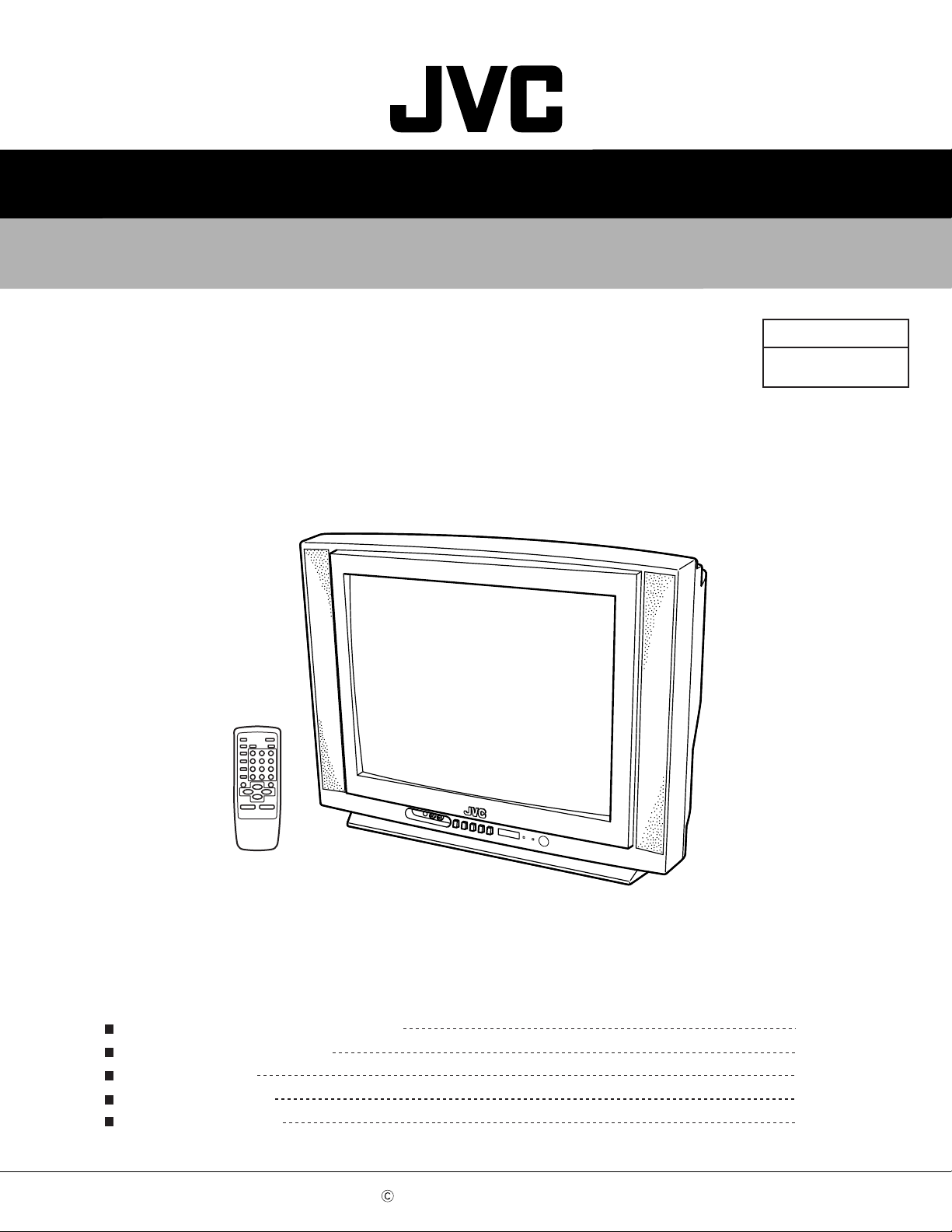
SCHEMATIC DIAGRAMS
COLOUR TELEVISION
AV-21D41
AV-21D71
AV-21D41/BK
AV-21D71/VT
CD-ROM No.SML200112
BASIC CHASSIS
CG
CONTENTS
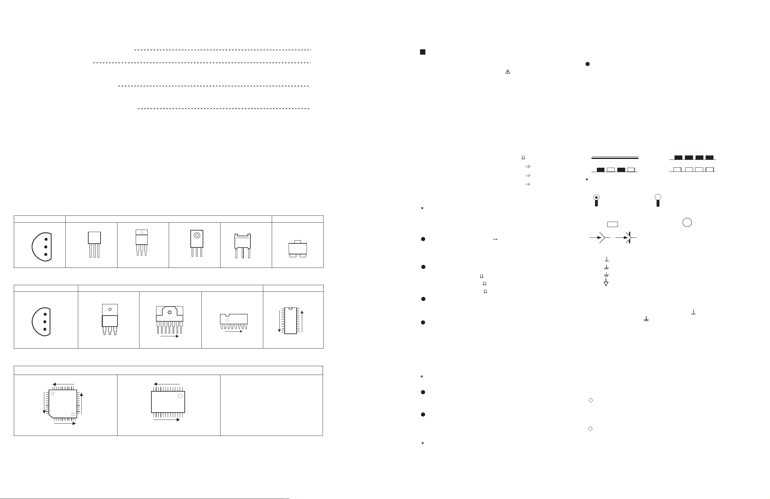
NOTE ON USING CIRCUIT DIAGRAMS
SEMICONDUCTOR SHAPES
BLOCK DIAGRAM
CIRCUIT DIAGRAMS
PATTERN DIAGRAMS
COPYRIGHT 2001 VICTOR COMPANY OF JAPAN, LTD.
2-1
2-2
2-3
2-5
2-13
No.51925
Nov. 2001
Page 2
AV-21D41
STANDARD CIRCUIT DIAGRAM
NOTE ON USING CIRCUIT DIAGRAMS
1.SAFETY
The components identified by the symbol and shading are
critical for safety. For continued safety replace safety critical
components only with manufactures recommended parts.
2.SPECIFIED VOLTAGE AND WAVEFORM VALUES
The voltage and waveform values have been measured under the
follo win g c onditions.
(1)Input signal : Colour bar signal
(2)Setting positions of
each knob/button and
variable resistor
(3)Internal resistance of test er
:DC 20k
/V
(4)Oscil loscope sweeping time
:H
20µS/div
:V
5mS/div
:Others
Sweeping time is
specified
(5)Voltage values
:All DC voltage values
Sin ce th e vo l tage val ue s of si gn a l cir cui t va ry to some ex ten t
according to adjustments, use them as reference values.
3.INDICATION OF PARTS SYMBOL [EXAMPLE]
In the PW board
:R1209
R209
4.INDICATIONS ON THE CIRCUIT DIAG RAM
(1)Resistors
Resistance value
No unit :[
]
K
:[K
]
M
Rated allowable power
No indicatio n :1/ 16 [W]
Others :As specified
Type
No indicatio n
:Carbon resistor
OMR
:Oxide metal film resistor
MFR
:Metal film resistor
MPR
:Metal plate resistor
UNFR
:Uninflammable resistor
FR
:Fusible resistor
Composition re sistor 1/2 [W] is specified as 1/2S or Comp.
(2)Capacitors
: Original setting position
when shipped
5.N OT E FOR RE PAIRIN G SERVICE
This model's power circuit is partly different in the GND. The
difference of the GND is shown by the LIVE : ( ) side GND and the
ISOLATED(NEUTRAL) : ( ) side GND.Therefore, care must be
taken for the following points.
(1)Do not touch the LIVE side GND or the LIVE side GND and the
ISOLATED(NEUTRAL) side GND simultaneously. If the above
caution is not respected, an electric shock may be caused.
Therefore, make sure that the power cord is surely removed from
the receptacle when, for example, the chassis is pulled out.
(2)Do no t short between the LIVE side GND and ISOLATED(NEUTRAL)
side GND or never measure with a measuring apparatus measure
with a measuring apparatus ( oscilloscope, etc.) the LIVE side GND
and ISOLATED(NEUTRAL) side GND at the same time.
If the above precaution is not respected , a fuse or any parts will be broken.
Since the circuit diagram is a standard one, the circuit and
circ uit con stant s may be subj ect to chan ge f or i mprovem ent
without any not ic e.
NOTE
Due improvement in performance, some part numbers show
in the circuit diagram may not agree wi th those i ndicated in
the part list.
When ordering parts, pl ease use t he numbers t hat appear
in the Parts List.
Type
MM
:M eta lized mylar cap ac i tor
PP
:Polypropylene capacitor
MPP
:Metalized polypropylene capacitor
MF
:Metalized f ilm capacitor
TF
:Thin film capacitor
BP
:Bipolar electrolytic capacitor
TAN
:Tantalum capacitor
(3)Coils
No unit
:[
µ
H]
Others
:As specified
(4)Power Supply
:B1
:9V
:5V
Respective voltage values are indicated
(5)Test point
:T est point
:Only test point display
(6)Connecting method
:Connector
:Wrapping or soldering
:Receptacle
(7)Ground symbol
:LIVE side ground
:ISOLATED(NEUTRAL) side ground
:EARTH ground
:DIGITAL ground
:[M ]
Capacitance value
1 or higher :[pF]
less than 1
:[µF]
Withstand voltage
No indication :DC 50[V]
Others :DC withstand voltage [V]
AC indicated
:AC withstand voltage [V]
Electrolytic Capacitors
47/50[Example]:Capacitance value [µF]/withstand voltage[V]
No indication
:Ceramic capacitor
:B2 (12V)
AV-21D71
CONTENTS
AV-21D41
AV-21D71
SEMICONDUCTOR SHAPES
BLOCK DIA GRAM
CIRCUIT DIAGRAMS
MAIN PWB CI RCUIT DIAGRA M
P ATTERN DIAGRAMS
MAIN PWB & CRT SOCKET PATTERN
SEMICONDUCTOR SHAPES
TRANSISTOR
BOTTOM VIE W
E
C
B
ECB
BCE
(G)(D)(S)
IC
B O TT OM VI EW F R O NT VIEW TO P VI EW
CHIP IC
2-2
OUT
E
IN
N
N
N
1
N
IN OUTE
FRONT VI EW
1 N
TO P VI EW
ECB
1
N
No.51925
TO P VI EW
CHIP TR
ECB
1 N
1
2-2
2-3
2-5
2-13
C
BE
N
Nov. 2001 No. 51925
Page 3
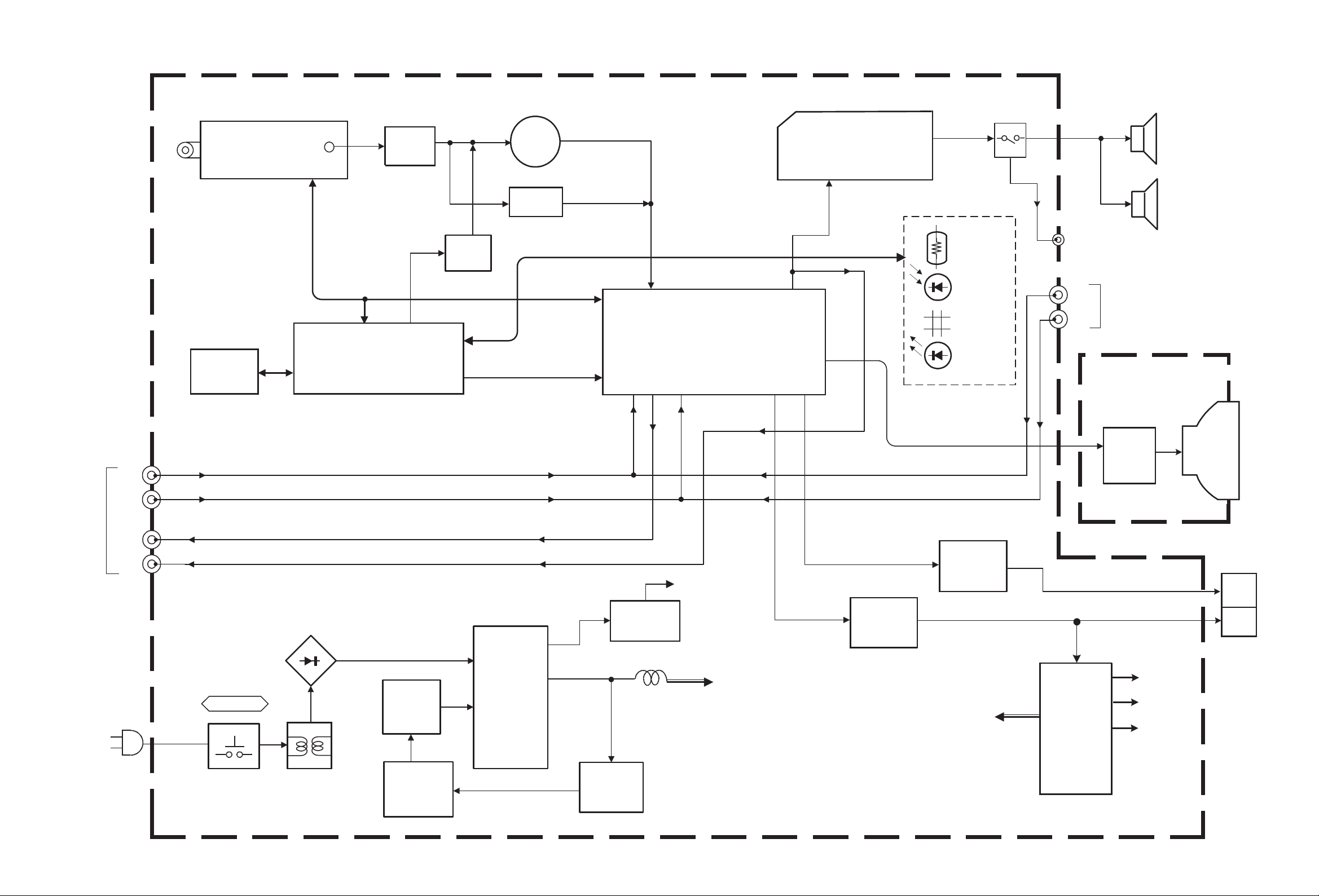
BLOCK DIAGRAM
Q102
IF AMP
SF101
VIDEO
AUDIO
IC701
MICRO COMPUTER
IC201
1 CHIP DECODER
RGB
10.11.12
29
30
38
24
MAIN PWB
IC702
MEMORY
IC651
AUDIO AMP
SP
AUDIO
3
8
OSD
RGB
SF102
SCL/SDA
B1
IC421
VERT.OUT
Q522
H.OUT
DY(V)
DY(H)
DEF.YOKE
H.OUT V .OUT
H.OUT
V .OUT
42
46
SCL
SDA
POWER SW
IN
OUT
AC IN
Q103
SW
HEAD
PHONE
CF901
30.31.32
SAW
EXT
RGB
TU001
TUNER
IF
T921
SW
TRANSF.
IC921
POWER
REG.
PC921
VOLTAGE
FEEDBACK
IC941
ERROR
AMP
IC971
5/9V REG.
REG.
D901
RECT
R / G /B
V01
CRT
CRT SOCKET
PWB
RGB
DRV
ECO
REMOCON
KEY
IND.
VIDEO
AUDIO
T522
HVT
FOCUS
SCREEN
EHV
B1
SP
18.19
3.58/
OTH
25
37.38
6.7.8
VIDEO
IN
VIDEO
OUT
AUDIO
IN
AUDIO
OUT
SCL
SDA
SP
OUT
VIDEO
AUDIO
REAR
FRONT
IN
AV-21D41
AV-21D71
AV-21D41
AV-21D71
No.51925
2-3 2-4
No.51925
Page 4
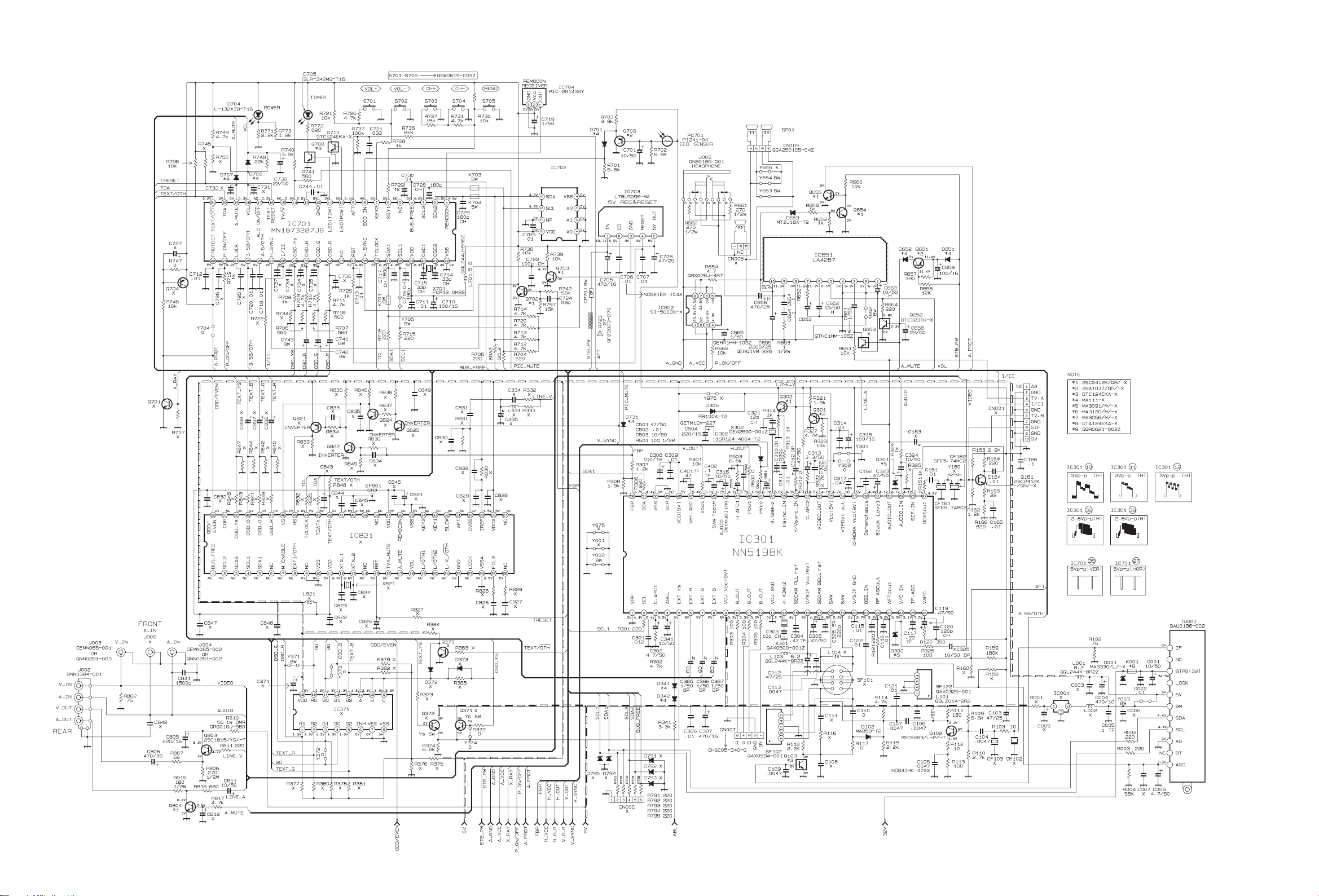
AV-21D41
AV-21D71
AV-21D41
AV-21D71
CIRCUIT DIAGRAMS MAIN PWB CIRCUIT DIAGRAM
(1/2) [AV-21D41]
AT24C08-21DTT2
MEMORY
QAS0086-001
MAIN PWB
SCG-1303A-BK
1K
2W
10/50
.0015
No.51925 No.51925
2-5 2-6
Page 5
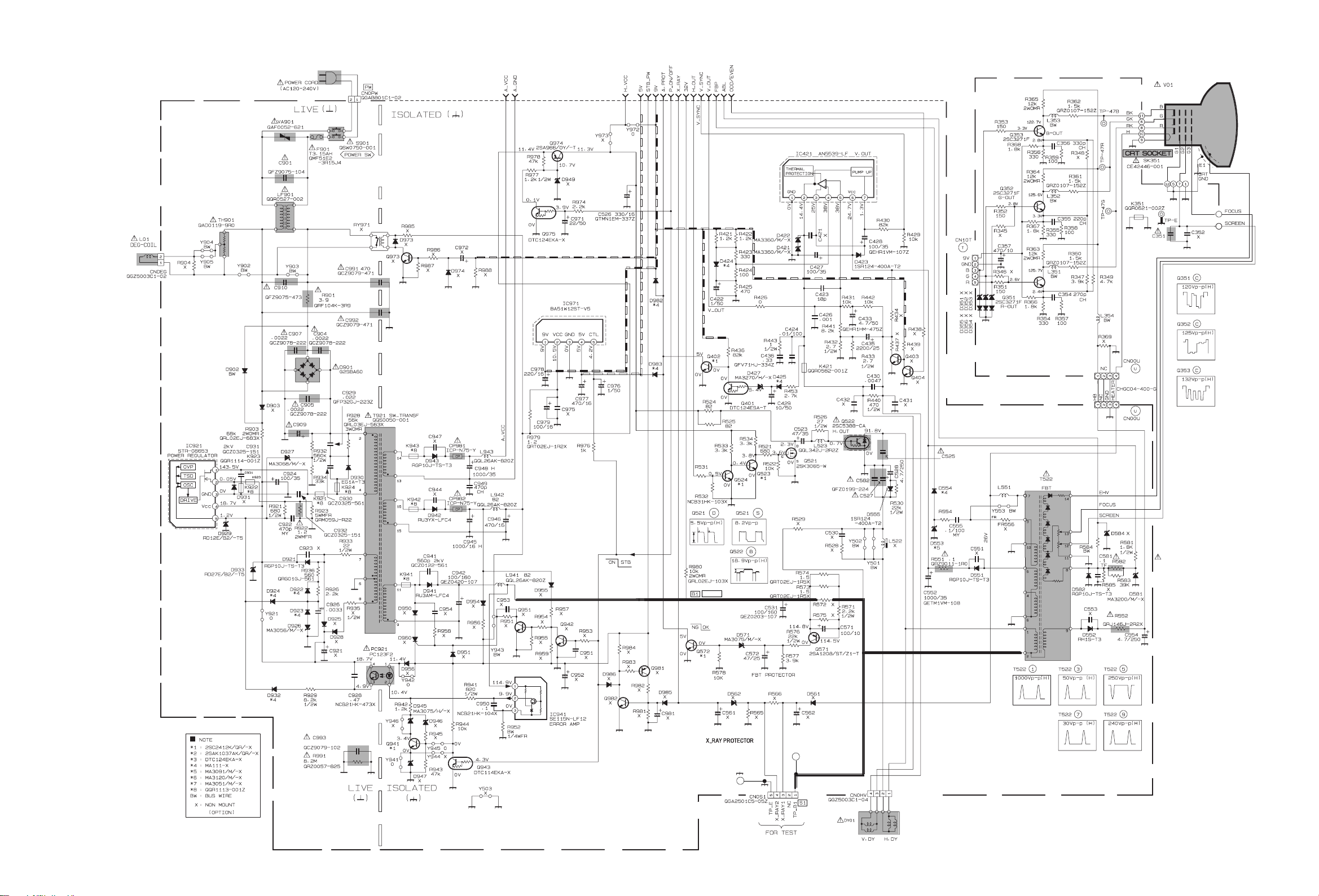
MAIN PWB CIRCUIT DIAGRAM (2/2) [AV-21D41]
MPP
MAIN PWB
SCG-1303A-BK
(1/2)
CRT SOCKET PWB
SCG-1303A-BK
(2/2)
(Within MAIN PWB)
QMPR010-200-E2
.1 AC275V MPP
.047 AC275V MPP
10W
470p AC250V
470p AC250V
AC250V
AC250V
AC250V
.001 AC250V
1W
TP-E
( )
TP-91
( B1 )
CE20336-00A
.22 250V MPP
.22 250V MPP
4.7K
114.5V
1/2W
680
.01 1.5KVH
QFZ0200-103
QQLZ034-500
QQH0069-001
2.2 1/4W
R582
22K 1/10W
NRSA02J-223X
.001
3KV
QCZ0121-102
A51LMV20X
PICTURE TUBE
QQW0006-001
120/400
QEZ0476-127
QFZ0199-224
AV-21D41
AV-21D71
AV-21D41
AV-21D71
No.51925
2-7 2-8
No.51925
Page 6

MAIN PWB CIRCUIT DIAGRAM (1/2) [AV-21D71]
AV-21D41
AV-21D71
AV-21D41
AV-21D71
QAS0086-001
AT24C08-21DTT2
MEMORY
56p
X
BW
BW
2W
MAIN PWB
SCG-1304A-CK
220
220
220
No.51925 No.51925
2-9 2-10
470/16
Page 7

MAIN PWB CIRCUIT DIAGRAM (2/2) [AV-21D71]
AV-21D41
AV-21D71
AV-21D41
AV-21D71
CELD029-004J6
QAD0119
-9RO
QMP40D0-200J5
QQR0527-002
.047 AC275V
AC250V
A51JSW51X07
PICTURE TUBE
2SC3271F
.1
2SC3271F
X
470p
UNFR
470p
AC250V
AC275V
AC275V
BW
3.9 1/10W
QRF104K-3R9
AC250V
120/400
X
X
X
X
X
X
X
X
18p
.001
2.7
2.7
82
82
X
.0047
.470
2SC3271F
CRT SOCKET PWB
(Within MAIN PWB)
SCG-1304A-CK
(2/2)
.001 AC250V
MPP
.009 1.5KVH
10K
.25 250V MPP
QFZ0199-254
.3 250V MPP
QFZ0199-304
X
1.5
114.5V
3.9K
TP-91
( B1)
TP-E
( )
1W
X
MAIN PWB
(1/2)
1SR124-400A-T2
2.2K
22K
CE41210
-008
4.7/
250
QFZ0200-902
820
1/2W
QQLZ018-860
QQH0070-001
2.2 1/4W
R582
22K 1/10W
NRSA02J-223X
No.51925
SCG-1304A-CK
2-11 2-12
(ITC)
No.51925
Page 8
AV-21D41
AV-21D71
AV-21D41
AV-21D71
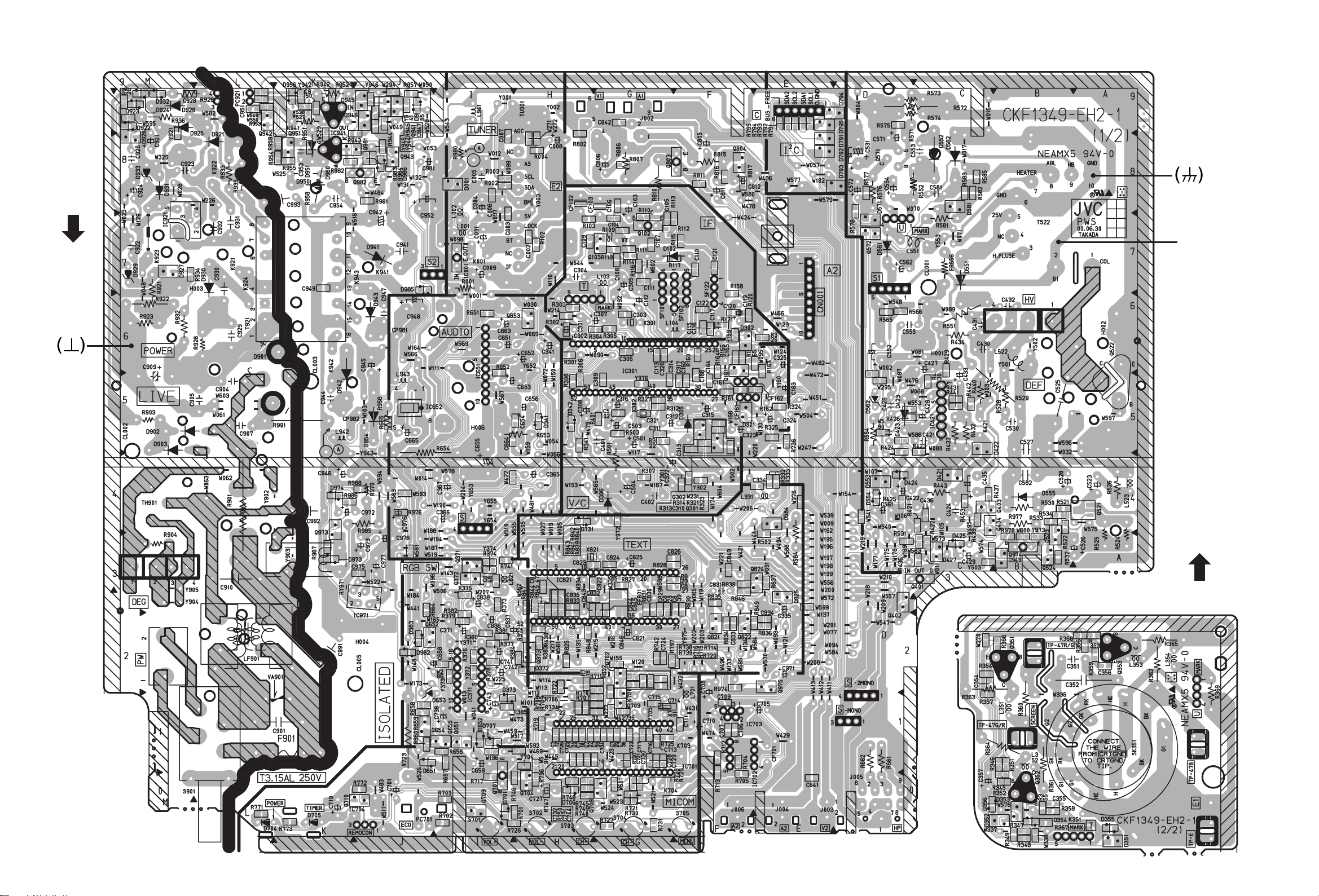
PATTERN DIAGRAMS MAIN PWB & CRT SOKET PWB PATTERN
FRONT
MAIN PWB
TP-E
TP-91
(B1)
CRT SOCKET PWB
No.51925 No.51925
2-13 2-14
TOP
82
,2$$
Page 9

VICTOR COMPANY OF JAPAN, LIMITED
HOME AV NETWORK BUSINESS UNIT. 12, 3-chome, Moriya-cho, Kanagawa-ku, Yokohama, Kanagawa-prefecture, 221-8528, Japan
AV21D41BK-H #3
AV21D71VT-H #3
Printed in Japan
VP 0111
DP6060
 Loading...