

Page 1
SCHEMATIC DIAGRAMS
COLOUR TELEVISION
AV21BF5ENS
AV21BF5EES
CD-ROM No.SML200201
AV21BF5ENS
AV21BF5EES
CONTENTS
NOTE ON USING CIRCUIT DIAGRAMS
SEMICONDUCTOR SHAPES
BLOCK DIAGRAM
WAVEFORM DIAGRAMS
CIRCUIT DIAGRAMS
PATTERN DIAGRAMS
VOLTAGE TABLES
COPYRIGHT 2002 VICTOR COMPANY OF JAPAN, LTD.
2-1
2-2
2-3
2-4
2-5
2-11
2-15
No.51879
Jan. 2002
Page 2
AV21BF5ENS
STANDARD CIRCUIT DIAGRAM
NOTE ON USING CIRCUIT DIAGRAMS
1.SAFETY
The components identified by the symbol and shading are
critical for safety. For continued safety replace safety critical
components only with manufactures recommended parts.
2.SPECIFIED VOLTAGE AND WAVEFORM VALUES
The voltage and waveform values have been measured under the
foll owin g condition s.
(1)Input signal : Colour bar signal
(2)Setting positions of
each knob/button and
variable resistor
(3)Internal resistance of tester
:DC 20k
/V
(4)Oscilloscope sweeping time
:H
20µS/div
:V
5mS/div
:Others
Sweeping time is
specified
(5)Voltage values
:All DC voltage values
Sin ce the voltage values of signal circui t vary to some extent
according to adjustments, use them as reference values.
3.INDICATIONS ON THE CIRCUIT DIAGRAM
(1)Resistors
Resistance value
No unit :[
]
K
:[K
]
M
Ty pe
No indication
:Carbon resistor
OM R
:Oxi de metal film resistor
MFR
:Met al film resi stor
MPR
:Metal plate resistor
UNFR
:Uninflammable resistor
FR
:Fusible resistor
Composition resist or 1/2 [W] is spec ified as 1/2S or Comp.
(2)Capacitors
: Original setting position
when shipped
4.NOTE FOR REPAIRING SERVICE
This model's power circuit is partly different in the GND. The
difference of the GND is shown by the LIVE side GND and the
ISOLATED(NEUTRAL) side GND.Therefore, care must be
taken for the following points.
(1)Do not touch the LIVE side GND or the LIVE side GND and the
ISOLATED(NEUTRAL) side GND simultaneously. If the above
caution is not respected, an electric shock may be caused.
Therefore, make sure that the power cord is surely removed from
the receptacle when, for e xample, the chassis is pulled out.
(2)Do not short between the LIVE side GND and ISOLATED(NEUTRAL)
side GND or never measure with a measuring apparatus measure
with a measuring apparatus ( oscilloscope, etc.) the LIVE side GND
and ISOLATED(NEUTRAL) side GND at the same time.
If the above precaution is not respected , a fuse or any parts will be broken.
Since the circuit diagram is a standard one, the circuit and
circuit constants may be subject to change for improvement
without a ny notice.
NOTE
Due improvement in performance, some part numbers show
in th e circui t diagram may not agree with those i ndicated in
the part list.
When ordering parts, please use the numbers that appear
in the Part s List.
Ty pe
MM
:Metalized mylar capacitor
PP
:Polypropylene capacitor
MPP
:Metalized polypropylene capacitor
MF
:Metalized film capacitor
TF
:Thin film capacitor
BP
:Bipolar electrolytic capacitor
TAN
:Tantalum capacitor
(3) Coi ls
No unit
:[
µ
H]
Others
:As specified
:[M ]
Capacitance valu e
1 or higher :[pF]
less than 1
:[µF]
Withstand voltage
No indication :DC50[V]
Others :DC withstand voltage [V]
AC indicated
:AC withstand voltage [V]
Electrolytic C apaci tors
47/50[Example]:Capacitance value [µF]/withstand voltage[V]
No indication
:Ceramic capacitor
AV21BF5ENS
AV21BF5EES
AV21BF5EES
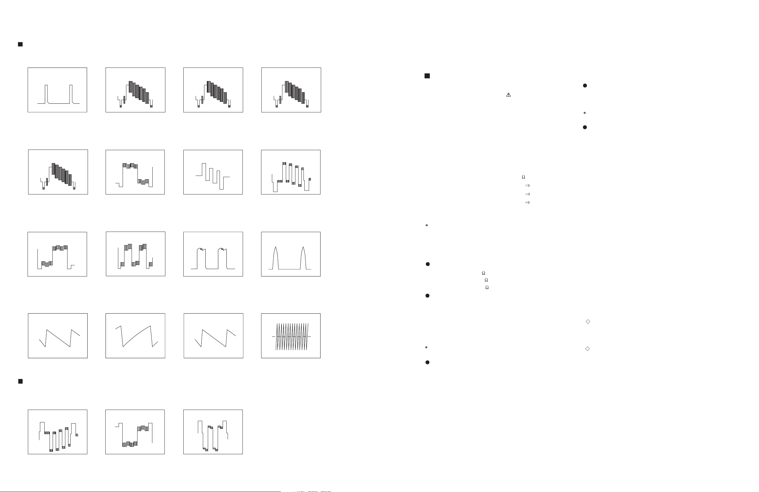
WAVEFORM DIAGRAMS
MAIN PWB
AV21BF5ENS
AV21BF5EES
Q802 D
IC401 6pin IC050 6pin IC050 17pin
8Vp-p(H) 1.7Vp-p(H) 0.7Vp-p(H) 1.4Vp-p(H)
IC401 17pin
IC401 30pin
2-4
0.7Vp-p(H) 0.8Vp-p(H) 0.9Vp-p(H) 2Vp-p(H)
IC401 20pin
IC401 21pin
2Vp-p(H) 2Vp-p(H) 1Vp-p(H) 450Vp-p(H)
0.6Vp-p(V) 4.8Vp-p(V) 0.5Vp-p(V) 1.2Vp-p
CRT SOCKET PWB
35Vp-p(H) 35Vp-p(H) 35Vp-p(H)
IC401 29pin IC401 19pin
IC901 9pinIC901 8pinIC901 7pin
No.51879
Q605 CIC401 40pin
IC501 34pinIC701 9pinIC401 47pin IC701 1pin
Jan. 2002 No. 51879
Page 3
AV21BF5ENS
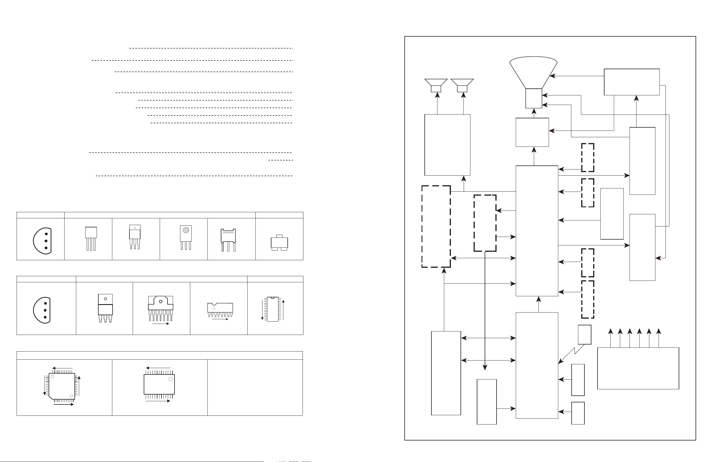
TV-TEXT CONTROLLER
SDA 555X
PLL TUNER
UV1315/6
SERVICE
CONNECTOR
CTI &
COMB FILTER
SPEAKERS
8R 6/12W
RGB AMP.
TDA 6108
8R 6/12W
I2C
AUDIO
OUTPUTS
TDA2615/6
TDA2614(MONO)
SMPS
(Mc44604)
NVM KEYPAD
VIDEO SWITCH
TEA6415
VERTICAL
OUTPUT TDA8351/6
HORIZONTAL
OUTPUT
FBT
CRT
IR.
FRONTAV
115/150VDC
+12VDCAud.
-12VDCAud.
12VDC
8VDC
5VDC
3.3V st-by
2.5V st-by
SCART1 SCART2 SVHS
VIDEO PROCESSOR
TDA 884X
MSP 34X0D
DIGITAL SOUND PROCESSOR
AV21BF5EES
CONTENTS
AV21BF5ENS
AV21BF5EES
BLOCK DIAGRAM
SEMICONDUCTOR SHAPES
BLOCK DIAGRAM
WAVEFORM DIAGRAMS
CIRCUIT DIAGRAMS
MAIN PWB CIRCUIT DIAGRAM
MULTISOUND PWB CIRCUIT DIAGRAM
CRT SOCKET PWB CIRCUIT DIAGRAM
FRONT CONTROL PWB CIRCUIT DIAGRAM
HEADPHONE JACK PWB CIRCUIT DIAGRAM
PATTERN DIAGRAMS
MAIN PWB PATTERN
MULTISOUND, HEADPHONE JACK, CRT SOCKET & FRONT CONTROL PWB PATTERN
VOLTAGE TABLES
SEMICONDUCTOR SHAPES
TRANSISTOR
BOTTOM V IEW
E
C
B
IC
BOTTOM VIEW FRONT VIEW TOP VIEW
OUT
E
IN
CHIP IC
N
N
ECB
IN OUTE
FRONT VI EW
BCE
(G)(D)(S )
1 N
TOP VIEW
ECB
ECB
1 N
1
CHIP TR
1
2-2
2-3
2-4
2-5
2-7
2-9
2-9
2-9
2-11
2-13
2-15
TOP VIEW
C
BE
N
2-2
N
1
N
N
No.51879No.51879
2-3
Page 4

CIRCUIT DIAGRAMS
MAIN PWB CIRCUIT DIAGRAM
AV21BF5ENS
AV21BF5EES
AV21BF5ENS
AV21BF5EES
No.51879
MAIN PWB
VE-20073865(AV21BF5EES), VE-20073855(AV21BF5ENS)
2-5 2-6
No.51879
Page 5

MUL TISOUND PWB CIRCUIT DIAGRAM
AV21BF5ENS
AV21BF5EES
AV21BF5ENS
AV21BF5EES
MULTISOUND PWB
VE-20078991(AV21BF5EES, AV21BF5ENS)
No.51879 No.51879
2-7 2-8
Page 6

CRT SOCKET PWB CIRCUIT DIA GRAM
CRT SOCKET PWB
VE-20074437
AV21BF5ENS
AV21BF5EES
AV21BF5ENS
AV21BF5EES
HEADPHONE JACK PWB CIRCUIT DIA GRAM
HEADPHONE JACK PWB
VE-20080166
FRONT AV PWB CIRCUIT DIAGRAM
FRONT AV PWB
VE-20079114
No.51879
2-9 2-10
No.51879
Page 7

PATTERN DIAGRAMS MAIN PWB PATTERN
FRONT
AV21BF5ENS
AV21BF5EES
AV21BF5ENS
AV21BF5EES
No.51879 No.51879
2-11 2-12
Page 8

MULTISOUND PWB PATTERN
AV21BF5ENS
AV21BF5EES
AV21BF5ENS
AV21BF5EES
CRT SOCKET PWB PATTERN
TOP TOP
TOP
FRONT AV PWB PATTERN
HEADPHONE JACK PWB PATTERN
TOP
No.51879
2-13 2-14
No.51879
Page 9

VOLTAGE TABLES
MAIN PWB
IC050
PIN NO.
1
2
3
4
5
6
7
8
9
10
IC401
PIN NO.
1
2
3
4
5
6
7
8
9
10
11
12
13
14
15
16
17
18
19
20
21
22
23
24
25
26
27
28
IC801
PIN NO.
1
2
3
IC802
PIN NO.
1
2
3
4
5
6
7
8
IC804
PIN NO.
1
2
3
IC807
PIN NO.
1
2
3
VOLTAGE
2.8
4.5
2.8
4.5
2.9
3.1
0
2.9
7.8
3.9
VOLTAGE
0.1
3.6
0
0
2.4
2.8
4.5
4.5
6.6
0.1
3.6
7.8
3.8
0
3
0.1
3.6
3.6
3
3
3
3
3.6
3.6
3.6
0.1
0.1
2.7
VOLTAGE
12.4
11.3
0
VOLTAGE
11.9
11.6
0.1
0
0.9
0.1
0.2
0.2
VOLTAGE
3.4
2.1
12.4
VOLTAGE
9.9
0
5
PIN NO.
PIN NO.
29
30
31
32
33
34
35
36
37
38
39
40
41
42
43
44
45
46
47
48
49
50
51
52
53
54
55
56
PIN NO.
PIN NO.
9
10
11
12
13
14
15
16
IC805
PIN NO.
11
12
13
14
15
16
17
18
19
20
4
5
6
1
2
3
VOLTAGE
3.7
0
4.0
4.0
2.1
4.0
2.7
4.0
0
2.8
VOLTAGE
2.4
2.3
0
0
0
2.5
2.5
4.7
7.8
2.9
4.9
0.1
0.1
3.4
3.9
0
3.4
2.4
2.4
4.5
4.5
2.0
3.7
3.8
4.2
2.6
3.0
3.3
VOLTAGE
2.6
11.9
0.1
VOLTAGE
0.9
2.6
2.4
0.1
3.1
2.5
2.5
2.5
VOLTAGE
12.3
0
7.9
IC701
PIN NO.
1
2
3
4
5
IC100
PIN NO.
1
2
3
4
5
VOLTAGE
2.3
2.3
15
7.1
0
VOLTAGE
0
12.7
0
0
-12.8
PIN NO.
6
7
8
9
PIN NO.
6
7
8
9
AV21BF5ENS
AV21BF5EES
VOLTAGE
44.5
7.5
0.3
7.1
VOLTAGE
0
12.8
0
0
AV21BF5ENS
AV21BF5EES
Note)
Although the symbol numbers of the level
drive transistor and level output
transistor are indicated as Q604 and Q606 on
the wiring diagram, the numbers
are indicated as Q601 and Q605 on the
substrate, respectively. The following
table shows the silk-printed symbol numbers
on the substrate.
E(D) C(S) B(G)
Q055 0.1 7.8 0.1
Q100 0 12.7 0
Q501 2.5 0 2.5
Q512 5.4 3.4 4.8
Q514 0 4.8 0
Q515 4.5 3.2 2.3
IC501
PIN NO.
1
2
3
4
5
6
7
8
9
10
11
12
13
14
15
16
17
18
19
20
21
22
23
24
25
26
VOLTAGE
0.7
0
0
3.3
3.3
3.3
3.3
0
2.4
0
3.4
0.8
2.4
0
0.1
0
0
2.4
0.3
0.2
0
2.1
3.3
3.8
3.1
3.0
PIN NO.
27
28
29
30
31
32
33
34
35
36
37
38
39
40
41
42
43
44
45
46
47
48
49
50
51
52
VOLTAGE
0
0
0
3.3
3.3
3.3
3.3
0.5
0.5
0
2.4
0.2
0.2
0.2
0
2.4
0
3.3
0
3.4
3.4
3.4
3.4
3.4
3.4
3.4
Q516 3.2 4.5 2.4
Q517 4.5 3.2 2.4
Q518 3.2 4.5 2.4
Q601 0 0 0.1
Q605 0 --- 0.1
Q701 0 0 0
Q702 0 0 0.6
Q802 167 0 0.1
Q805 0 0 0.6
Q806 0 0 0.6
Q807 0 11.3 0
Q809
Cathode:11.3V
Anode:0V
Control terminal:2.4V
IC502
PIN NO.
1
2
3
4
VOLTAGE
0
0
0
0
No.51879 No.51879
PIN NO.
5
6
7
8
VOLTAGE
3
3
3.4
3
2-15 2-16
MULTI SOUND PWB
IC301
PIN NO.
1
2
3
4
5
6
7
8
9
10
11
12
13
14
15
16
17
18
19
20
21
22
23
24
25
26
27
28
29
30
31
32
VOLTAGE
2.5
0
0
4.9
0
0
4.9
0
4.5
4.5
2.4
2.4
2.4
0.1
0.1
0.1
0
4.8
0
0
0
0
0
4.9
0.1
0.1
0
0
0
0
0
0
IC304
PIN NO.
1
2
3
4
VOLTAGE
2.4
2.4
2.4
0
IC307
PIN NO.
10
11
12
13
14
Q301
VOLTAGE
1
2
3
4
5
6
7
8
9
E(D)
4.8
3.2
3.2
4.9
0
0.1
2.4
2.4
2.2
0
2.7
0
2.1
5.0
0
C(S)
4.8
CRT SOCKET PWB
IC901
PIN NO.
1
2
3
4
5
VOLTAGE
3.2
2.9
3.2
0
6.0
B(G)
4.1
PIN NO.
33
34
35
36
37
38
39
40
41
42
43
44
45
46
47
48
49
50
51
52
53
54
55
56
57
58
59
60
61
62
63
64
PIN NO.
5
6
7
8
PIN NO.
15
16
17
18
19
20
21
22
23
24
25
26
27
28
PIN NO.
6
7
8
9
VOLTAGE
3.7
3.7
0
3.7
3.7
6.8
7.8
6.5
0
3.6
3.7
3.7
0
3.7
3.7
0
3.7
3.7
0
3.7
3.7
2.6
3.7
0
4.9
0.1
0.1
0.1
0
2.3
2.3
0
VOLTAGE
2.4
2.4
2.4
4.9
VOLTAGE
0.1
0
4.3
3.0
3.5
3.3
3.3
3.3
3.5
4.5
0
3.4
0.1
0.1
VOLTAGE
0.1
0.1
0.1
0.1
Page 10

AV21BF5ENS
AV21BF5EES
VICTOR COMPANY OF JAPAN, LIMITED
HOME AV NETWORK BUSINESS UNIT. 12, 3-chome, Moriya-cho, Kanagawa-ku, Yokohama, Kanagawa-prefecture, 221-8528, Japan
Printed in Japan
VP 0201
DP2080
 Loading...