


Rev0.0
JSWAM83 Module
JSWAM83
9
Tri Band Module
USER Manual
Product Name :
Model Name :
Page1of
Rev0.0
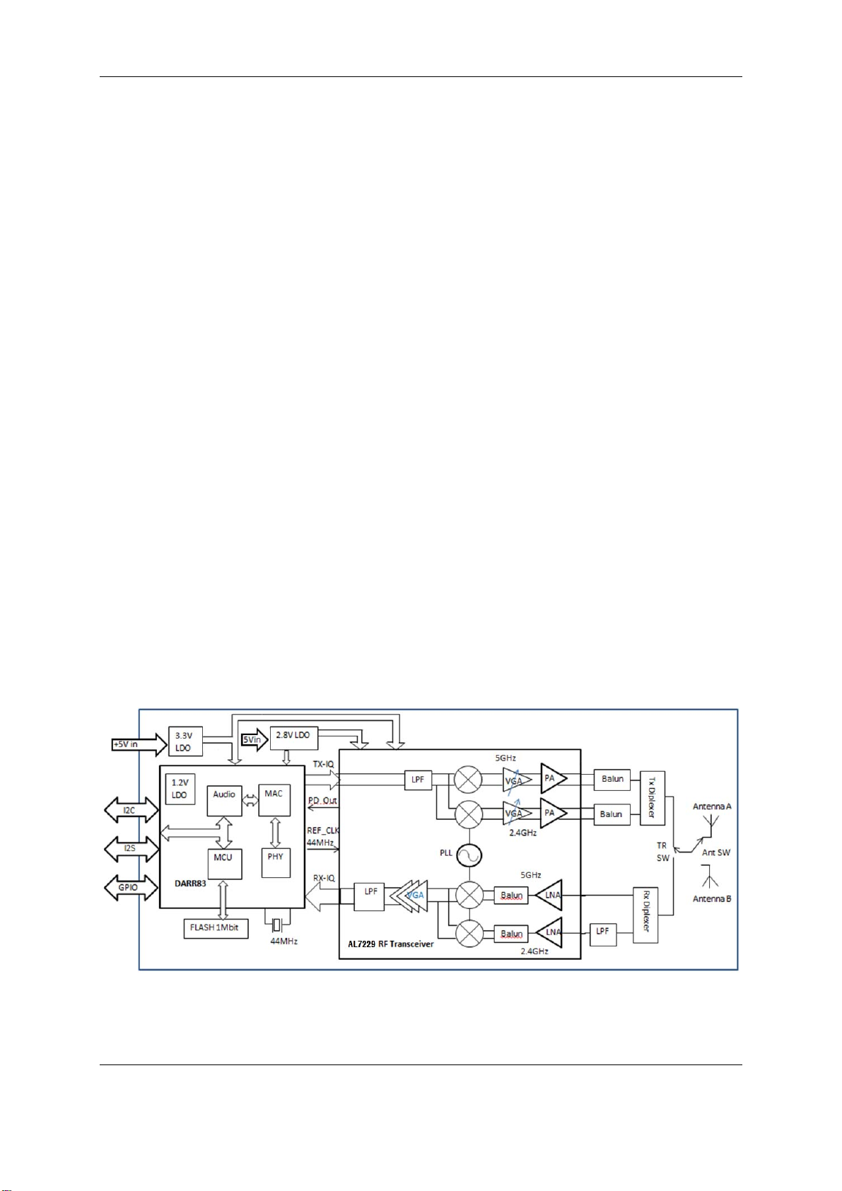
The JSWAM83 module is a wireless audio module (60X21mm)) based on the SMSC
Automatic Frequecncy Allocation.
JSWAM83 Block Diagram
9
1. Product Description
DARR83. This module can used to build an uncompressed wireless digital audio
transceiver operating in the 2.4GHz, 5.2GHz and 5.8GHz bands.
The wireless audio link supports up to two stereo audio streams and comes together with
additional features such as: data encryption, pairing functionality, bi-directional control
data messages, low power audio snooze mode,
The DARR83 chip itself provides the basic functions of Audio Processing and buffering, Data
Link Layer and Physical Layer. The WISP50S module integrates all functionality for a wireless
digital and analog audio connection, comprising:
2. Features
DARR83 Wireless Audio Processor
2.4GHz/ 5.2GHz/ 5.8 GHz RF Transceiver
Embedded Antennas
Digital audio interfaces (I
Integrated 24 bit stereo Audio DAC + Headphone AMP
Integrated 16 bit Audio ADC + Microphone AMP
Built-in SPI interface Flash
9 pins interface connector for power, audio output, control interface and GPIOs
Regulated 5V supply
2
S)
3.
Page2of
Rev0.0
9
Using RF Frequency
4. Description of operations
4.1 Operating Conditions ( 5 V 450 mA)
Symbol Parameter Min. Typ Max Unit
VCC Supply Voltage 4.7 5.0 5.25 V
Temp Operating Temperature 0 25 60 °C
4.2 RF Information
Parameter Value Unit
Modulation QPSK
2400 – 2483.5
RF Frequency range (band)
Audio Latency
5150 – 5250
5725 – 5875
Ch1 – 2412
Ch2 – 2436
Ch3 – 2464
Ch4 – 5180
Ch5 – 5210
Ch6 – 5240
Ch7 – 5736
Ch8 – 5726
Ch9 – 5814
20ms
MHz
MHz
Audio Bit Resolution
Audio Sampling Rate
Note: Country/ Region dependent.
16bit
48ksps
4.3 Receive mode
In receive mode, antenna diversity is supported. The single ended output of the TR switch is
connected to the RF LNA input through Diplexer and matching networks. Filtering and amplification is
all performed by the radio transceiver. The gain setting is controlled by the BB. The analog IQ outputs
are sampled by the BB by its integrated 22Msps dual channel 8bit ADC. This received data is
demodulated and fed to the audio processing engine controlling the audio function.
4.4 Transmit mode
In transmit mode, the audio engine transforms the audio data into packetized digital IQ signals. These
are in turn pulse-shaped before conversion by a 10bits 44Msps DAC to match to the analog IQ inputs
of the radio IC. The radio IC has programmable baseband filters to lower the RF spectrum side lobes
Page3of
Rev0.0
9
and to suppress the DAC image and the DAC spurious. The output power is programma ble. A power
detector (PD_out) on the radio IC enables close-loop TX power control. The differential RF PA outputs
are connected via a baluns and Diplexer to a transmit/receive switch with TX diversity option to the RF
connectors.
5. Clock and synthesizer frequencies
The main crystal is connected to the Baseband IC crystal oscillator. This in turn buffers this 44MHz
and feeds it to the radio IC.
In standard configurations, the DARR83 based DWPCIe83 module’s RF section runs at the following
frequencies:
2.4GHz Band: The RF oscillator runs at 2 times the programmed RF output frequency.
Channel RF frequency (in MHz) VCO frequency (in MHz)
1 2412 4824
2 2438 4876
3 2464 4928
5.2GHz Band: The RF oscillator runs at 2/3 times the programmed RF output frequency.
Channel RF frequency (in MHz) VCO frequency (in MHz)
1 5180 3453.33
2 5210 3473.33
3 5240 3493.33
5.8GHz Band: The RF oscillator runs at 2/3 times the programmed RF output frequency.
Channel RF frequency (in MHz) VCO frequency (in MHz)
1 5736 3824
2 5762 3841.33
3 5814 3876
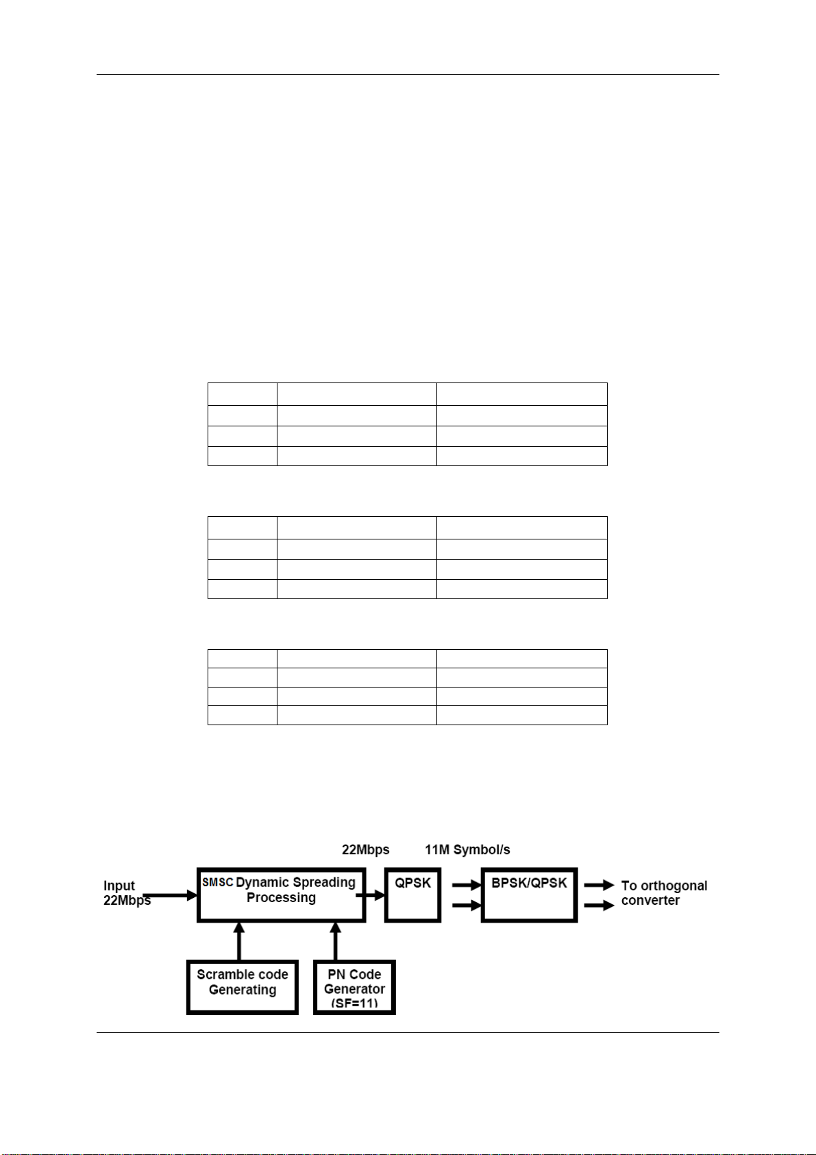
6. Modulation Diagram
Page4of
Rev0.0
9
7. Pin out interface connector
Pin information.
Pin Number Pin Name I/O Description
1 5V
2 5V
3 GPIO_2
4 GPIO_13
5 GPIO_14
6 /RESET(DARR_RST)
7 I2C_SCL_SLV
8 I2C_SDA_SLV
9 I2C_SCL_MST
10 I2C_SDA_MST
11 MCLK
12 GND
13 BCK_W
14 LRCK_W
15 GPIO_5
16 GPIO_11
17 MON_TXD
18 GIPO_6
19 GPIO_12
20 GPIO_3
21 GPIO_15
22 GPIO_4
23 GPIO_7
24 GND
PWR
PWR
I/O
I/O
I/O
I
I/O
I/O
I/O
I/O
I/O
GND
I/O
I/O
I/O
I/O
I/O
I/O
I/O
I/O
I/O
I/O
I/O
GND
Regulated 4.7V to 5.2V input
Regulated 4.7V to 5.2V input
PWM_RST#
MUTE
POWER_CTL
Reset Darr83
I2C serial clock Slave
I2C serial data Slave
I2C serial clock Master
I2C serial data Master
12.288MHz audio clock I/O
GND
I2S port W Bit Clock
I2S port W Left Right Clock
DAT_W
DAT_X
Serial sync Data, for test purposes
FW_SEL
IR_RST#
ID_SET#
RED_LED
BLUE_LED (UART_RXD)
IR_SD#(HW_MUTE)
GND
Page5of
Rev0.0
9
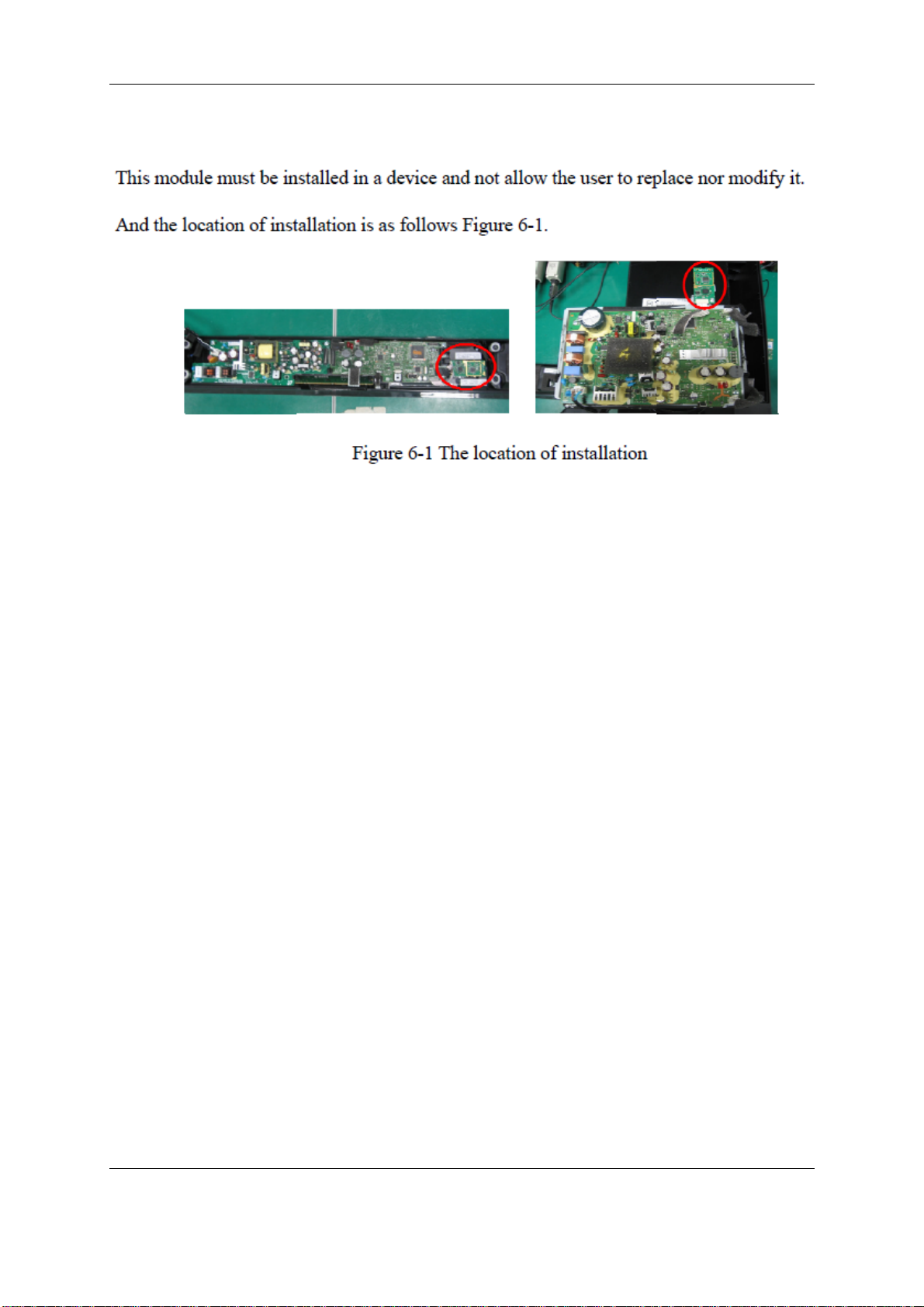
OEM Installation
8.
Page6of

9.

Rev0.0
between the radiator & your body and must not be co-located or operating in conjunction with
10. Notice
Page8of
9
any other antenna or transmitter, except in accordance with FCC multi-transmitter product
procedures.
FCC Statement
Federal Communication Commission Interference Statement
This equipment has been tested and found to comply with the limits for a Class B digital
device, pursuant to Part 15 of the FCC Rules. These limits are designed to provide
reasonable protection against harmful interference in a residential installation. This
equipment generates, uses and can radiate radio frequency energy and, if not installed and
used in accordance with the instructions, may cause harmful interference to radio
communications. However, there is no guarantee that interference will not occur in a
particular installation. If this equipment does cause harmful interference to radio or television
reception, which can be determined by turning the equipment off and on, the user is
encouraged to try to correct the interference by one of the following measures:
● Reorient or relocate the receiving antenna.
● Increase the separation between the equipment and receiver.
● Connect the equipment into an outlet on a circuit different from that to which the receiver
is connected.
● Consult the dealer or an experienced radio/TV technician for help.
FCC Caution:
Any changes or modifications not expressly approved by the party responsible for
compliance could void the user’s authority to operate this equipment.
This device complies with Part 15 of the FCC Rules. Operation is subject to the following two
conditions: (1) This device may not cause harmful interference, and (2) this device must
accept any interference received, including interference that may cause undesired operation.
For product available in the USA/Canada market, only channel 1~11 can be operated and
these channel assignments deal with only the 2.4 GHz range.
This device and its antenna(s) must not be co-located or operation in conjunction with any
other antenna or transmitter.
This device is going to be operated in 5.15~5.25GHz frequency range, it is restricted in
indoor environment only.
IMPORTANT NOTE:
FCC Radiation Exposure Statement:
This equipment complies with FCC radiation exposure limits set forth for an uncontrolled
environment. This equipment should be installed and operated with minimum distance 20cm
USERS MANUAL OF THE END PRODUCT:

Rev0.0
8
Labelling Requirements
The Original Equipment Manufacturer(OEM) must ensure that FCC labelling
requirement are met. This includes a clearly visible label on the outside of the OEM
enclosure specifying the appropriate JUNSUNGTECH Co., Ltd. FCC identifier for this
product as well as the FCC Notice above.
The FCC identifier is FCC ID: XNKJSWAM83. In any case the end product must be
labeled exterior with "Contains FCC ID: XNKJSWAM83".
If the size of the end product is larger than 8x10Cm, then the following with Part15.19
statement has to also be available on the label: This device complies with Part15 of
FCC rules. Operation is subject to the following two conditions:
(1) this device may not cause harmful interference and (2) this device must accept any
interference received, including interference that may cause undesired operation.
Page 9 of 9
In the users manual of the end product, the end user has to be informe d to keep at least
20cm separation with the antenna while this end product is installed and operated. The
end user has to be informed that the FCC radio-frequency exposure guidelines for an
uncontrolled environment can be satisfied. The end user has to also be informed that
any changes or modifications not expressly approved by the manufacturer could void the
user's authority to operate this equipment. If the size of the end product is smaller than
8x10cm, then additional FCC part 15.19 statement is required to be availa ble in the
users manual: This device complies with Part 15 of FCC rules. Operation is subject to
the following two conditions: (1) this device may not cause harmful interference and (2)
this device must accept any interference received, including int erference that may cause
undesired operation.
Page8of
A. Test Procedures for Design and Verification (Confidential)

OQC
JUNSUNGTECH Co., Ltd.
JSWAM83
3-Band Module
2019.02.20
REPORT
PAGE : 1 / 2
Draft Check Approval
/ / /
1. Inspection Lot Information (Lot NO : 0312SG - 001)
Product Customer Inspection Day
Model Lot Size 768 EA Inspector R.W.I. & L.K.S.
Method
PCS/REV
No.
G-Ⅱ, 1 time Sample(n) 80 EA
Maj:0.25, Min:0.4 Level Nomal Min 0/1
/
/ ~ WH03-C17-302-0792
/
/ Min 0
Serial No.
NG Q'ty
AQL(AC/RE)
WH03-C17-302-0025
Maj 0
1st 2nd 3rd
Maj 0/1
2. Inspection Criteria
Function OK /NG PCB Assembly OK /NG
Mechanical OK /NG Package OK /NG
3. Sample Serial No.
WH03-C17 WH03-C17 WH03-C17 WH03-C17 WH03-C17 WH03-C17 WH03-C17 WH03-C17 WH03-C17 WH03-C17
302-0260 302-0261 302-0258 302-0264 302-0256 302-0262 302-0257 302-0259 302-0254 302-0255
WH03-C17 WH03-C17 WH03-C17 WH03-C17 WH03-C17 WH03-C17 WH03-C17 WH03-C17 WH03-C17 WH03-C17
302-0263 302-0253 302-0201 302-0195 302-0199 302-0203 302-0200 302-0193 302-0194 302-0196
WH03-C17 WH03-C17 WH03-C17 WH03-C17 WH03-C17 WH03-C17 WH03-C17 WH03-C17 WH03-C17 WH03-C17
302-0204 302-0198 302-0197 302-0107 302-0103 302-0104 302-0105 302-0106 302-0108 302-0100
WH03-C17 WH03-C17 WH03-C17 WH03-C17 WH03-C17 WH03-C17 WH03-C17 WH03-C17 WH03-C17 WH03-C17
302-099 302-097 302-0102 302-0098 302-0101 302-0403 302-0404 302-0405 302-0406 302-0408
WH03-C17 WH03-C17 WH03-C17 WH03-C17 WH03-C17 WH03-C17 WH03-C17 WH03-C17 WH03-C17 WH03-C17
302-0360 302-0359 302-0358 302-0356 302-0355 302-0357 302-0401 302-0402 302-0398 302-0400
4. Note 5. Approval
Design
Change
NG
Infomation
Remark

REPORT
3-Band Module
JSWAM83
2019.02.20
OQC
JUNSUNGTECH Co., Ltd.
PAGE : 2 / 2
Draft Check Approval
/ / /
1. Inspection Lot Information (Lot NO : 0312SG - 001)
Product Customer Inspection Day
Model Lot Size 768 EA Inspector R.W.I. & L.K.S.
Method
PCS/REV
No.
G-Ⅱ, 1 time Sample(n) 80 EA
Maj:0.25, Min:0.4 Level Nomal Min 0/1
/
/ ~ WH03-C17-302-0792
/
/ Min 0
Serial No.
NG Q'ty
AQL(AC/RE)
WH03-C17-302-0025
Maj 0
1st 2nd 3rd
Maj 0/1
2. Inspection Criteria
Function OK /NG PCB Assembly OK /NG
Mechanical OK /NG Package OK /NG
3. Sample Serial No.
WH03-C17 WH03-C17 WH03-C17 WH03-C17 WH03-C17 WH03-C17 WH03-C17 WH03-C17 WH03-C17 WH03-C17
302-0397 302-0399 302-0353 302-0354 302-0352 302-0350 302-0349 302-0351 302-0438 302-0436
WH03-C17 WH03-C17 WH03-C17 WH03-C17 WH03-C17 WH03-C17 WH03-C17 WH03-C17 WH03-C17 WH03-C17
302-0433 302-0437 302-0435 302-0434 302-0647 302-0648 302-0646 302-0645 302-0643 302-0644
WH03-C17 WH03-C17 WH03-C17 WH03-C17 WH03-C17 WH03-C17 WH03-C17 WH03-C17 WH03-C17 WH03-C17
302-0517 302-0518 302-0520 302-0522 302-0744 302-0741 302-0740 302-0739 302-0742 302-0743
4. Note 5. Approval
Design
Change
NG
Infomation
Remark
※ Remark (OK : ○, NG : X, No Relation : - )
JUNSUNGTECH Co., Ltd.
JSWAM83
JSWAM83 Inspection List
2
3
4
Cofiguration
Connection
Lot No Model Buyer
Appearance
0312SG-001
Inspection Point
Black Spot/Line, White Spots, Scratch,
1○
Dust
Visual Area of Molding Parts Be compared with limit samples (MA)
3○
Uneven edge fitting Refer to Outgoing Inspection Standard
4○
Gaps
5○
Silk Screen Printing
6○
Spray Be compared with limit samples (MA)
7○
Labeling
8○
Decision
Refer to Outgoing Inspection Standard
Refer to Outgoing Inspection Standard
Omitted or missed silk printing (MA)
Refer to Outgoing Inspection Standard
ED:01
Criteria
Mechanicals
Basic
Function
RF
Test
PBA
Condition
Packing
Remark
1○
Key Stick
2○
Rubber Endurance
3○
Headset Separation Force 8 Nf : by push-pull gauge (MI)
4○
Car Kit Separation Force
5○
Charger Locking
6○
Information Display
1○
○
○
Call Display Display incomming call No., answer call (MA)
4○
Receiver & Mic Without noise, can hear callee's voice (MA)
5○
6○
Channel Power
1○
Occupied Bandwidth
2○
Sprious Emission
3○
4○
1○
Board Assembling
2○
Labeling
1○
Contents
2○
1.8~3.5 Nf : by push-pull gauge (MA)Key Stroke
1.6 Nf : by push-pull gauge (MA)
16 Nf : by push-pull gauge (MI)
10 Nf : by push-pull gauge (MI)
90 degree (MI), 45 degree (MA)
Be compared with product specifiaction (MA)
After power On/Off, hold configuration Data (MA)
Display phone No, signal strength, battery indi.(MA)
For 1 hour, must not broken (MI)Long Duration Call
4~7 dBm (MA)
0~26 MHz (MI)
Pass (MI)
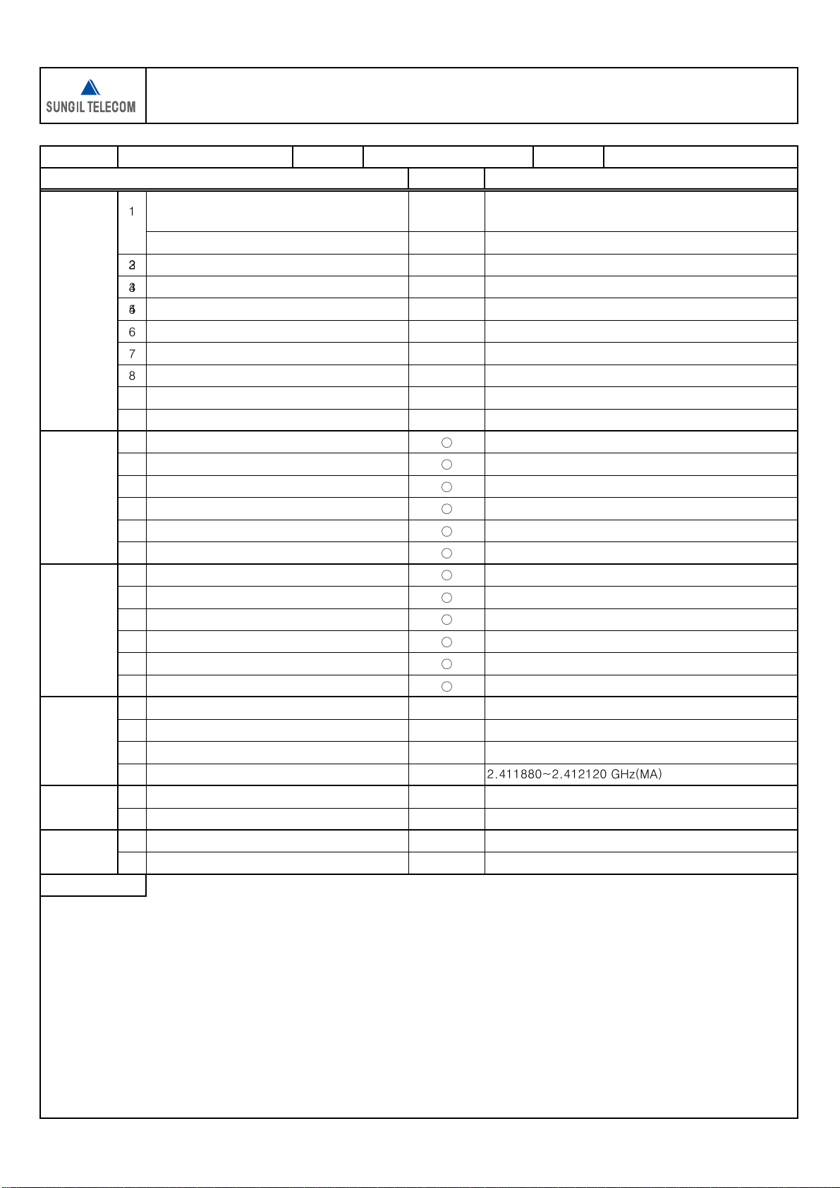
2.411880~2.412120 GHz(MA)Frequency Error
Refer to Outgoing Inspection StandardSoldering
Refer to Outgoing Inspection Standard
Refer to Outgoing Inspection Standard
Refer to Outgoing Inspection Standard

1. Product Information
y
JSWAM83
2019-02-20
JUNSUNGTECH
JUNSUNGTECH Co., Ltd.
RF TEST DATA SHEET
MODEL
LOT NO
0312SG001
Measure Da
2. Measure Data
No
WH
1 - - 302 - 0260
WHWH03C17
2 - - 302 - 261
3 - - 302 - 258
WH
4 - - 302 - 264
WH
5 - - 302 - 256
WH
6 - - 302 - 262
WH
7 - - 302 - 257
WH
8 - - 302 - 259
WH
9 - - 302 - 254
WH
10 - - 302 - 255
WH
11 - - 302 - 263
WH
12 - - 302 - 253
WH
13 - - 302 - 201
WH
14 - - 302 - 195
WH
15 - - 302 - 199
WH
16 - - 302 - 203
WH
17 - - 302 - 200
WH
18 - - 302 - 193
WH
19 - - 302 - 194
WH
20 - - 302 - 196
WH
21 - - 302 - 264
WH
22 - - 302 - 198
WH
23 - - 302 - 197
WH
24 - - 302 - 107
WH
25 - - 302 - 103
WH
26 - - 302 - 104
WH
27 - - 302 - 105
WH
28 - - 302 - 106
WH
29 - - 302 - 108
WH
30 - - 302 - 100
WH
31 - - 302 - 99
WH 03C17
32 - - 302 - 97
WH 03C17
33 - - 302 - 102
WH 03C17
34 - - 302 - 98
WH 03C17
35 - - 302 - 101
WH
36 - - 302 - 403
WH 03C17
37 - - 302 - 404
WH 03C17 4.7
38 - - 302 - 405
WH 03C17
39 - - 302 - 406
Serial No
03C17
03C17
03C17
03C17
03C17
03C17
03C17
03C17
03C17
03C17
03C17
Decision
Location
Channel Power
4~7
[㏈m]
5.8
4.6 15.2
5.0
4.5
4.6 15.2
4.9 15.3
5.4
5.0 15.7 PASS 2.41197
5.1
4.8
5.2 15.3 PASS 2.41199
5.1 14.9 PASS 2.41199
5.2
5.0 15.3 PASS 2.41196
4.6
5.5 15.4 PASS 2.41191
5.2
4.6 15.2 PASS 2.41198
4.9 15.3 PASS 2.41199
Occupied BW
Instrumnent
Spurious Emission
0~26
[㎒]
15.2
15.5 PASS 2.41198
15.1 PASS 2.41203
15.3
15.1 PASS
15.2
15.0 PASS 2.41197
15.3 PASS
15.6 PASS
Spetrum Analyzer(E4404B)
PASS
PASS 2.41197
PASS 2.41196
PASS
PASS
PASS
PASS 2.4119003C17 4.7 15.3
PASS 2.4119803C17 4.4 15.3
PASS 2.4119703C17 4.8 15.4
PASS 2.4119703C17 5.1 15.4
PASS 2.4119703C17 5.7 15.2
PASS 2.4119903C17 4.7 15.3
PASS 2.4119603C17 5.0 15.2
PASS 2.4119803C17 4.0 15.4
PASS 2.4119703C17 5.2 15.0
PASS 2.4119903C17 5.0 14.8
PASS 2.4120103C17 4.9 15.6
PASS 2.4119803C17 4.8 15.1
PASS 2.4119303C17 4.9 15.6
PASS 2.4119703C17 5.1 15.3
PASS 2.4119903C17 5.2 15.2
PASS 2.4119903C17 5.0 14.8
PASS 2.4119903C17 4.9 15.2
PASS 2.4119803C17 5.2 15.4
PASS 2.41199
PASS15.1
PASS 2.41198
OK / NG
Freq. Error
2.41188~2.41212
[㎓]
2.4120003C17
2.41190
2.4119903C17 4.5 15.5
2.41199
2.41198
2.41198
2.41201
Page : 1 of 2

No
JUNSUNGTECH Co., Ltd.
WH 03C17 5.2
40 - - 302 - 408
WH 03C17
41 - - 302 - 360
WH 03C17 5.4
42 - - 302 - 359
WH 03C17
43 - - 302 - 358
WH 03C17 5.1
44 - - 302 - 356
WH 03C17
45 - - 302 - 355
WH 03C17 4.7
46 - - 302 - 357
WH 03C17
47 - - 302 - 401
WH 03C17 4.7
48 - - 302 - 402
WH 03C17
49 - - 302 - 398
WH 03C17 5.1
50 - - 302 - 400
WH 03C17
51 - - 302 - 397
WH 03C17 5.2
52 - - 302 - 399
WH 03C17
53 - - 302 - 353
WH 03C17 4.7
54 - - 302 - 354
WH 03C17
55 - - 302 - 352
WH 03C17 5.0
56 - - 302 - 350
WH 03C17
57 - - 302 - 349
WH 03C17 5.0
58 - - 302 - 351
WH 03C17
59 - - 302 - 438
WH 03C17 4.4
60 - - 302 - 436
WH 03C17
61 - - 302 - 433
WH 03C17 5.9
62 - - 302 - 437
WH 03C17
63 - - 302 - 435
WH 03C17 6.3
64 - - 302 - 434
WH 03C17
65 - - 302 - 647
WH 03C17 5.9
66 - - 302 - 648
WH 03C17
67 - - 302 - 646
WH 03C17 6.5
68 - - 302 - 645
WH 03C17
69 - - 302 - 643
WH 03C17 5.6
70 - - 302 - 644
WH 03C17
71 - - 302 - 517
WH 03C17 6.3
72 - - 302 - 518
WH 03C17
73 - - 302 - 520
WH 03C17 5.5
74 - - 302 - 522
WH 03C17
75 - - 302 - 744
WH 03C17 5.4
76 - - 302 - 741
WH 03C17
77 - - 302 - 740
WH 03C17 5.7
78 - - 302 - 739
WH 03C17
79 - - 302 - 742
WH 03C17 5.5
80 - - 302 - 743
Statistic
Serial No
MIN
MAX
AVG
특기사항
Channel Power
4~7
[㏈m]
4.7 15.3 PASS 2.41200
5.1 15.3 PASS 2.41196
4.8 15.4 PASS 2.41197
5.1 15.2 PASS 2.41198
4.8 15.3 PASS 2.41199
5.2 15.2 PASS 2.41198
4.9 15.3 PASS 2.41197
6.7 15.4 PASS 2.41196
4.6 15.3 PASS 2.41199
5.0 15.5 PASS 2.41199
5.8 15.4 PASS 2.41197
5.6 15.7 PASS 2.41199
5.5 15.0 PASS 2.41196
5.7 15.6 PASS 2.41199
6.3 15.0 PASS 2.41197
5.7 15.3 PASS 2.41197
5.9 15.3 PASS 2.41200
6.8 15.4 PASS 2.41196
6.0 15.5 PASS 2.41197
5.7 15.6 PASS 2.41196
4.0 14.8
6.8
5.2 15.3 2.41197
Occupied BW
0~26
[㎒]
15.4 PASS
15.4 PASS
15.3 PASS
15.4 PASS
15.2 PASS
15.2 PASS
15.5 PASS
15.2 PASS
15.3 PASS
15.3 PASS
15.4 PASS
15.5 PASS
15.8 PASS
15.3 PASS
15.0 PASS
15.0 PASS
15.1 PASS
15.4 PASS
15.5 PASS
15.4 PASS
15.5 PASS
Spurious Emission
PASS
Freq. Error
2.41188~2.41212
[㎓]
2.41197
2.41196
2.41198
2.41197
2.41200
2.41198
2.41196
2.41197
2.41199
2.41196
2.41198
2.41195
2.41199
2.41196
2.41196
2.41197
2.41194
2.41196
2.41197
2.41196
2.41195
2.41190
2.4120315.8
Page : 2 of 2

B. PCB Layout (Confidential)

C. BOM (Confidential)
D. Antenna Specification (Confidential)

 Loading...