


LSI3144A
Encoder/Linear Scale
Counter Card
User's Manual (V1.4)
健昇科技股份有限公司
JS AUTOMATION CORP.
新北市汐止區中興路 100 號 6 樓
6F., No.100, Zhongxing Rd.,
Xizhi Dist., New Taipei City, Taiwan
TEL:886-2-2647-6936
FAX:886-2-2647-6940
http://www.automation.com.tw
http://www.automation-js.com/
E-mail:control.cards@automation.com.tw

1
Correction record
Version
Record
1.0 firmware version 1.0 up
1.1
add 5.2 JM1 High speed signal I/O connector (on board)
1.2 Modify 6.2 Output diagram
1.3 Modify 2 Features-Delete Software key function
1.4
1.
Modify Notes on hardware installation
2.
Add Warranty
3.
Change orientation of JM1 and JF1 connector (chapt. 5)
4.
Add specifications to each input and output (chapt. 6)

2
Contents
1. Forward ............................................................................................................................................... 5
2. Features ............................................................................................................................................... 6
2.1 Main card .................................................................................................................................... 6
2.2 DIN rail mounted wiring board ................................................................................................... 6
3. Specifications ...................................................................................................................................... 7
3.1 LSI3144A Main card ................................................................................................................... 7
3.2 ADP3144DIN DIN rail mounted wiring board ........................................................................ 8
3.3 ADP3144ADIN DIN rail mounted wiring board (high speed type) ........................................ 8
4. Layout and dimensions ....................................................................................................................... 9
4.1 LSI3144A Main card ................................................................................................................... 9
4.2 ADP3144DIN DIN rail mounted wiring board ...................................................................... 10
4.3 ADP3144ADIN DIN rail mounted wiring board (high speed type) ...................................... 10
5. Pin definitions for 68P SCSI connector ............................................................................................ 11
5.1 JM1 High speed signal I/O connector (on bracket) .................................................................. 11
5.2 JM1 High speed signal I/O connector (on board) ..................................................................... 12
5.3 JF1 Front view of connector ..................................................................................................... 13
6. I/O Interface diagram ........................................................................................................................ 14
6.1 Input diagram ............................................................................................................................ 14
6.2 Output diagram ......................................................................................................................... 15
6.3 High speed port I/O diagram (JM1) .......................................................................................... 16
7. External wiring diagram ................................................................................................................... 17
8. Hardware settings ............................................................................................................................. 19
8.1 Card ID setting .......................................................................................................................... 19
8.2 Matched wiring board setting ................................................................................................... 19
9. Applications ...................................................................................................................................... 20
10. Ordering information ........................................................................................................................ 21

Notes on hardware installation
Please follow step by step as you are installing the control cards.
1. Be sure your system is power off.
2. Be sure your external power supply for the wiring board is power off.
3. Plug your control card in slot, and make sure the golden fingers are put in right contacts.
4. Fasten the screw to fix the card.
5. Connect the cable between the card and wiring board.
6. Connect the external power supply for the wiring board.
7. Recheck everything is OK before system power on.
8. External power on.
Congratulation! You have it.
For more detail of step by step installation guide, please refer the file
“..\download\Supplemental_technical_data\Step_by_step_installation_of_Contrl_Card.pdf “ on the CD
come with the product or download the complementary documents from
http://www.automation.com.tw/common/Supplemental_technical_data.htm
Warning:
Some computer BIOS has “Auto detect DIMM/PCI clock” option, be sure to switch to
“DISABLE” else in some cases the PCI add on cards will not be detected by windows at cold start.
3

4
Warranty
The LSI3144A is warranted against defects in materials and workmanship for a period of two years
from the date of shipment, as evidenced by receipts or serial no. on board. JS automation Corp. will, at
its option, repair or replace product that proves to be defective during the warranty period. This warranty
includes parts, labor and shipping costs of returning.
Except as specified herein, JS automation Corp. makes no warranties, express or implied, and
specifically disclaims any warranty of merchantability or fitness for a particular purpose. Customer’s
right to recover damages caused by fault or negligence on the part of JS automation Corp. shall be
limited to the amount theretofore paid by the customer. JS automation Corp. will not be liable for
damages resulting from loss of data, profits, use of products, or incidental or consequential damages,
even if advised of the possibility thereof. This limitation of the liability of JS automation Corp. will
apply regardless of the form of action, whether in contract or tort, including negligence. Any action
against JS automation Corp. must be brought within one year after the cause of action accrues.
JS automation Corp. shall not be liable for any delay in performance due to causes beyond its reasonable
control. The warranty provided herein does not cover damages, defects, malfunctions, or service failures
caused by owner’s failure to follow the JS automation Corp. installation, operation, or maintenance
instructions; owner’s modification of the product; owner’s abuse, misuse, or negligent acts; and power
failure or surges, fire, flood, accident, actions of third parties, or other events outside reasonable control.
If any defect occurs, you should email to us as the following form to get the fast response:
Detailed Company Information
Company/Organization:
Contact Person:
E-mail:
Address:
Country:
Tel/Fax:
Web Site:
Product information
product model:
serial no.:
Environment to Use: such as CPU board, Operating System, target application...
description of defect: (as detail as possible)

5
1. Forward
Thank you for your selection of PCI bus LSI3144A quadrature encoder/linear scale interface
card.
In the field of automation, encoder and linear scale as feedback or measuring element is common
used in the microprocessor control system. But for the versatile application in PC based control, only
a few selections you can make.
We integrate 4 axes (channels) in one card with the state of the art technology of FPGA chip and
provide photo/magnetic coupler isolation and experienced functions such as external triggered latch
or load counter, auto increment compare equal or FIFO pre-programmed compare equal output to
trigger external devices. The LSI3144A comes with new FIFO of PWM function. The compare out
triggers the position FIFO and the PWM FIFO that makes different PWM output at different line
interval.
Low cost and high performance makes this card a better choice to use in the servo control
feedback, 3D measuring system and other applications which are concerning encoder or linear scale.
Other encoder/linear scale interface card:
LSI3101 one-axis Quadrature Encoder Counter Card
(up to 8MHz quadrature input) (PCI bus
LSI3101A one-axis Quadrature Encoder Counter Card
(up to 16MHz quadrature input) (PCI bus
LSI3181 one-axis Quadrature Encoder Counter Card with 8 position offset comparators
(up to 16MHz quadrature input) (PCI bus)
LSI3104 4 axes quadrature encoder/linear scale counter card (PCI bus)
LSI3123A 3 axes quadrature encoder/linear scale counter card
with fast coordinate rebuild function (PCI bus)
LSI3134 4 axes quadrature encoder/linear scale counter card
with 1 axis FIFO compare mode (PCI bus)
LSI5123 3 axes quadrature encoder counter interface (USB)
LSI5123L 3 axes quadrature encoder counter interface (no external trigger latch mode) (USB)
LSI5123A 3 axes quadrature encoder counter interface (High noise immunity , Accurite linear
scale absolute coordinate mode) (USB)
Any comment is welcome,
)
)
please visit our website
http://www.automation.com.tw/
http://www.automation-js.com/ for the up to date information.

6
2. Features
2.1 Main card
2.1.1 PCI plug and play function with card ID for 16 identical cards
2.1.2 High noise immunity with magnetic/photo-coupler isolation
2.1.3 16 MHz max. Quadrature input rate
2.1.4 Four 32-bit counters
2.1.5 Quadrature, pulse/direction and up/down counting
2.1.6 Programmable multiple rate at X1, X2, X4
2.1.7 Load preset value to counter by external trigger or software trigger
2.1.8 Latch counter value by external trigger
2.1.9 Multiple counter reset (homing) modes
2.1.10 Differential or single-end input signal
2.1.11 Auto increment compare mode
2.1.12 FIFO position compare mode (X,Z axis)
2.1.13 FIFO PWM control (X,Z axis)
2.1.14 Programmable duration for Compare out and Clear out
2.1.15 Interrupt on external trigger, compare equal, borrow, carry and counter clear
2.1.16 Supports DIN rail mounted wiring board
2.2 DIN rail mounted wiring board
2.2.1 LED display for digital I/O
2.2.2 Application specific connectors
2.2.3 Step down s.p.s. for external 5V

7
3. Specifications
3.1 LSI3144A Main card
Counter input
3.1.1 Number of axes ─ 4, independent
3.1.2 Maximum quadrature input frequency ─ 16MHz
3.1.3 Maximum input pulse frequency ─ 16MHz
3.1.4 Encoder Type ─ Single-end or differential
3.1.5 Count per encoder cycle ─ X1, X2, X4 programmable (quadrature signal only)
3.1.6 Counter length ─ 32 Bits
3.1.7 Counter Mode ─ (QUADRATURE),(CLOCK/DIRECTION),
(UP CLOCK/ DOWN CLOCK)
3.1.8 Sample clock frequency ─ 198MHz
3.1.9 PCI data width ─ 32 Bits
3.1.10 Card ID ─ 4 bits
3.1.11 Input channel ─ 4 channels X, Y, Z and A, totally 4 compatible device units can be
hooked
Digital Input
3.1.12 Software homing (reset) counter method ─ 1 software trigger mode
3.1.13 Hardware homing (reset) counter method ─ 7 H/W trigger mode
3.1.14 External compare out mask off ─ INn(GATE), CLR
3.1.15 FIFO depth ─ 1023 (X,Z axis)
3.1.16 Compare out one shot duration ─ 1 ~ 16777215 us
3.1.17 Home ─ 1 per channel (Single end or differential)
3.1.18 Latch ─ 1 per channel (Single end or differential)
3.1.19 Clear counter ─ 1 per channel (Single end or differential)
3.1.20 General input ─ 1 per channel
3.1.21 Polarity ─ all input signals are software programmable
3.1.22 ON state ─ 2.8Vdc(max) 4.5mA(min)
3.1.23 OFF state ─ 8Vdc(min) 3mA(max)
3.1.24 Switching speed─ 2.2 K Hz (max) for general input
2 MHz (HOME, LATCH, CLEAR_IN)

8
Digital Output
General
3.1.25 Clear output ─ 1 per channel
3.1.26 General output ─ 1 per channel
3.1.27 Polarity ─ all output signals are software programmable
3.1.28 Output rating ─ 3A @250Vac, 30V dc (Relay wiring board)
1A @120Vdc (NMOS)
3.1.29 Switching speed ─ 20 K Hz (max) (MOS out only)
3.1.30 Card ID ─ 4 bits, 16 position
3.1.31 Photo isolation ─ All digital I/O and counter input
3.1.32 Insulation resistance ─ 1000Mohm (min) at 1000Vdc
3.1.33 Isolation voltage ─ 2500Vac 1 min
3.1.34 Connector ─ one 68 pin SCSI-II female connector
3.1.35 Operation temperature ─ 0 to +70 degree C
3.1.36 Storage temperature ─ -20 to +80 degree C
3.1.37 Operation humidity ─ 5-95% RH, non-condensing
3.1.38 Dimension ─ 151(W) * 110(H)mm , 6.0(W) * 4.4(H)in
3.2 ADP3144DIN DIN rail mounted wiring board
3.2.1 Connection cable ─ SCSI-II 68P cable to connect main and wiring board
3.2.2 Power supply voltage to wiring board ─ DC+24V
3.2.3 On board build-in s.p.s. ─ DC+5V 500mA (max)
3.2.4 Dimension ─ 86(W) * 204(L) * 53(H)mm , 3.4(W) * 8.1(L) * 2.1(H)in
3.3 ADP3144ADIN DIN rail mounted wiring board (high speed type)
3.3.1 Connection cable ─ SCSI-II 68P cable to connect main and wiring board
3.3.2 Power supply voltage to wiring board ─ DC+24V
3.3.3 On board build-in s.p.s. ─ DC+5V 500mA (max)
3.3.4 Dimension ─ 86(W) * 204(L) * 53(H)mm , 3.4(W) * 8.1(L) * 2.1(H)in

9
4. Layout and dimensions
4.1 LSI3144A Main card

10
4.2 ADP3144DIN DIN rail mounted wiring board
4.3 ADP3144ADIN DIN rail mounted wiring board (high speed type)

11
5. Pin definitions for 68P SCSI connector
PIN
DESCRIPTIONS
PIN
DESCRIPTIONS
13
NC
25
NC
12
NC
24
NC
11
NC
23
EXTG:
external ground
10
EXTG:
external ground
22
EXTG:
external ground
9
EXTG:
external ground
21
ACLR_CNTRO-:
negative differential output of
A_CLR_OUT;
general purpose/compare output
8
ACLR_CNTRO+:
positive differential output of
A_CLR_OUT;
general purpose/compare output
20
ACMP-:
negative differential output of
A_CMP;
general purpose/compare output
7
ACMP+:
positive differential output of
A_CMP;
general purpose/compare output
19
ZCLR_CNTRO-:
negative differential output of
Z_CLR_OUT;
general purpose/compare output
6
ZCLR_CNTRO+:
positive differential output of
Z_CLR_OUT;
general purpose/compare output
18
ZCMP-:
negative differential output of
Z_CMP;
general purpose/compare output
5
ZCMP+:
positive differential output of
Z_CMP;
general purpose/compare output
17
YCLR_CNTRO-:
negative differential output of
Y_CLR_OUT;
general purpose/compare output
4
YCLR_CNTRO+:
positive differential output of
Y_CLR_OUT;
general purpose/compare output
16
YCMP-:
negative differential output of
Y_CMP;
general purpose/compare output
3
YCMP+:
positive differential output of
Y_CMP;
general purpose/compare output
15
XCLR_CNTRO-:
negative differential output of
X_CLR_OUT;
general purpose/compare output
2
XCLR_CNTRO+:
positive differential output of
X_CLR_OUT;
general purpose/compare output
14
XCMP-:
negative differential output of
X_CMP;
general purpose/compare output
1
XCMP+:
positive differential output of
X_CMP;
general purpose/compare output
5.1 JM1 High speed signal I/O connector (on bracket)
Note: To use as general purpose output, the CMP or CLR_OUT pin must configured as general
purpose first and the paired differential signals work as general out (but on complementary
output level).

12
5.2 JM1 High speed signal I/O connector (on board)
PIN
DESCRIPTIONS
PIN
DESCRIPTIONS
1
XCMP+:
positive differential output of
X_CMP;
general purpose/compare output
2
XCMP-:
negative differential output of
X_CMP;
general purpose/compare output
3
XCLR_CNTRO+:
positive differential output of
X_CLR_OUT;
general purpose/compare output
4
XCLR_CNTRO-:
negative differential output of
X_CLR_OUT;
general purpose/compare output
5
YCMP+:
positive differential output of
Y_CMP;
general purpose/compare output
6
YCMP-:
negative differential output of
Y_CMP;
general purpose/compare output
7
YCLR_CNTRO+:
positive differential output of
Y_CLR_OUT;
general purpose/compare output
8
YCLR_CNTRO-:
negative differential output of
Y_CLR_OUT;
general purpose/compare output
9
ZCMP+:
positive differential output of
Z_CMP;
general purpose/compare output
10
ZCMP-:
negative differential output of
Z_CMP;
general purpose/compare output
11
ZCLR_CNTRO+:
positive differential output of
Z_CLR_OUT;
general purpose/compare output
12
ZCLR_CNTRO-:
negative differential output of
Z_CLR_OUT;
general purpose/compare output
13
ACMP+:
positive differential output of
A_CMP;
general purpose/compare output
14
ACMP-:
negative differential output of
A_CMP;
general purpose/compare output
15
ACLR_CNTRO+:
positive differential output of
A_CLR_OUT;
general purpose/compare output
16
ACLR_CNTRO-:
negative differential output of
A_CLR_OUT;
general purpose/compare output
17
EXTG:
external ground
18
EXTG:
external ground
19
EXTG:
external ground
20
EXTG:
external ground
Note: To use as general purpose output, the CMP or CLR_OUT pin must configured as general
purpose first and the paired differential signals work as general out (but on complementary
output level).
13
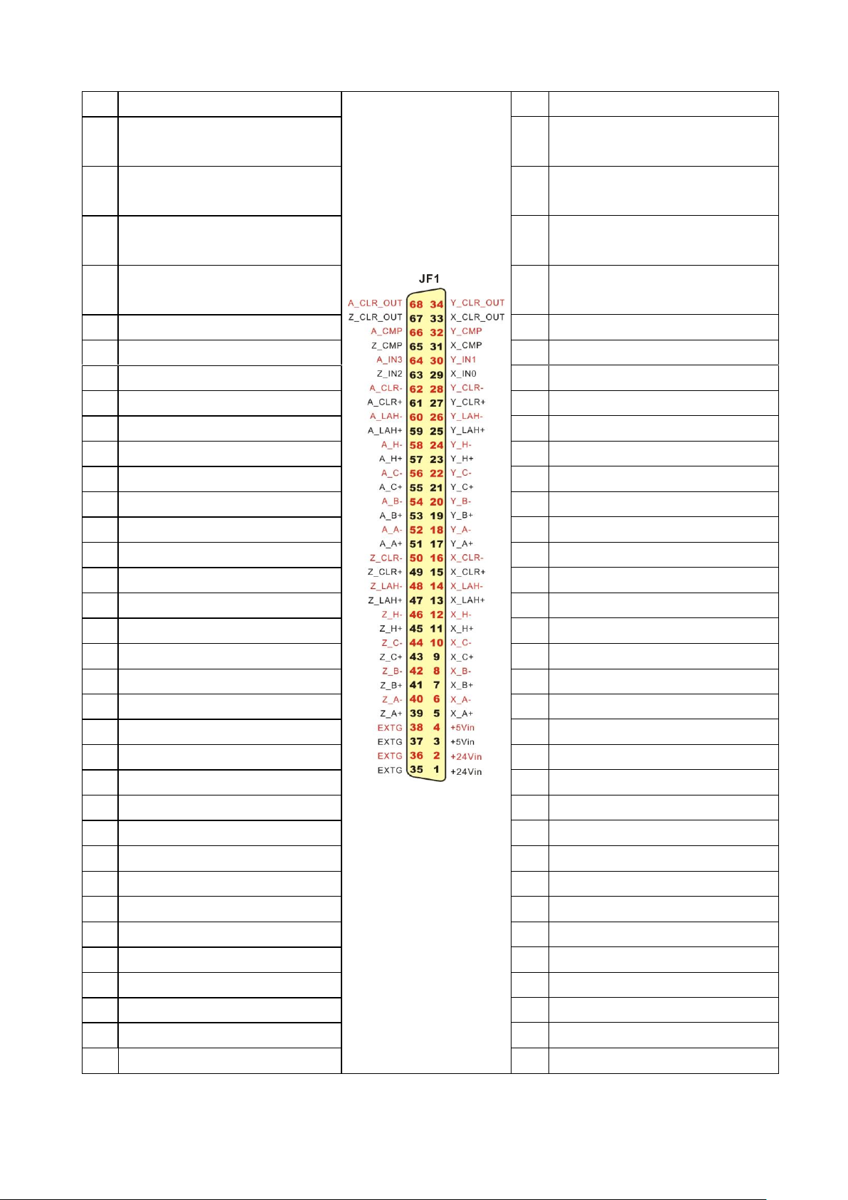
5.3 JF1 Front view of connector
PIN
DESCRIPTIONS
PIN
DESCRIPTIONS
68
A_CLR_OUT: clear
counter/general output
34
Y_CLR_OUT: clear
counter/general output
67
Z_CLR_OUT: clear
counter/general output
33
X_CLR_OUT: clear
counter/general output
66
A_CMP: general purpose output
32
Y_CMP: general purpose/compare
output
65
Z_CMP: general purpose/compare
output
31
X_CMP: general purpose/compare
output
64
A_IN3: general purpose input
30
Y_IN1: general purpose input
63
Z_IN2: general purpose input
29
X_IN0: general purpose input
62
A_CLR- : clear counter- input
28
Y_CLR- : clear counter- input
61
A_CLR+ : clear counter+ input
27
Y_CLR+ : clear counter+ input
60
A_LAH- : LATCH- input
26
Y_LAH- : LATCH- input
59
A_LAH+ : LATCH+ input
25
Y_LAH+ : LATCH+ input
58
A_H- : HOME- input
24
Y_H- : HOME- input
57
A_H+ : HOME+ input
23
Y_H+ : HOME+ input
56
A_C- : encoder C- phase input
22
Y_C- : encoder C- phase input
55
A_C+ : encoder C+ phase input
21
Y_C+ : encoder C+ phase input
54
A_B- : encoder B- phase input
20
Y_B- : encoder B- phase input
53
A_B+ : encoder B+ phase input
19
Y_B+ : encoder B+ phase input
52
A_A- : encoder A- phase input
18
Y_A- : encoder A- phase input
51
A_A+ : encoder A+ phase input
17
Y_A+ : encoder A+ phase input
50
Z_CLR- : clear counter- input
16
X_CLR- : clear counter- input
49
Z_CLR+ : clear counter+ input
15
X_CLR+ : clear counter+ input
48
Z_LAH- : LATCH- input
14
X_LAH- : LATCH- input
47
Z_LAH+ : LATCH+ input
13
X_LAH+ : LATCH+ input
46
Z_H- : HOME- input
12
X_H- : HOME- input
45
Z_H+ : HOME+ input
11
X_H+ : HOME+ input
44
Z_C- : encoder C- phase input
10
X_C- : encoder C- phase input
43
Z_C+ : encoder C+ phase input
9
X_C+ : encoder C+ phase input
42
Z_B- : encoder B- phase input
8
X_B- : encoder B- phase input
41
Z_B+ : encoder B+ phase input
7
X_B+ : encoder B+ phase input
40
Z_A- : encoder A- phase input
6
X_A- : encoder A- phase input
39
Z_A+ : encoder A+ phase input
5
X_A+ : encoder A+ phase input
38
EXTG : Ground
4
+5V : Regulated +5V out
37
EXTG : Ground
3
+5V : Regulated +5V out
36
EXTG : Ground
2
+24V : External DC +24V supply
35
EXTG : Ground
1
+24V : External DC +24V supply

14
6. I/O Interface diagram
For differential input :
A+/A-,B+/B-,C+/C-,H+/H-,
CLR+/CLR-,LAH+/LAH-
I/P specification:
VI **
VIL ** (max)
0.8V
VIH ** (min)
2V
VIT+ ** (max)
0.2V
VIT- ** (min)
-0.2V
Type 2 Input:
For input: IN0~IN3
I/P specification:
VI **
VIH ** (min)
10V
VIL ** (max)
5V
II **
IIH ** (max)
3mA
IIL ** (min)
6mA
6.1 Input diagram
Type1 input:

15
6.2 Output diagram
Type1 output:
For output: X,Y,Z,A(OUT/CLR_OUT)
(NMOS)
O/P specification:
VO **
VOH ** (max)
120Vdc
R
DS(on)
** (max)
0.4Ω
IO **
IOL ** (cont)
1A sink
Type2 output:
For output: X,Y,Z,A (OUT/CLR_OUT)
(Relay)
O/P specification:
VO **
VO ** (max)
250Vac/30Vdc
Io **
IO ** (cont)
3A(rms)
For output: X,Y,Z,A (OUT/CLR_OUT)
O/P specification:
VO **
VOH ** (max)
EXTVn
VOL ** (max)
0.8V
IO **
IOL ** (max)
40mA
6.2.1 ADP3144DIN
6.2.2 ADP3144ADIN

16
6.3 High speed port I/O diagram (JM1)
For output: X,Y,Z,A
(CMP+/CMP-, CLR_CNTRO+/CLR_CNTRO-)
O/P specification:
VO **
VOL ** (max)
0.5V @20mA sink
VOH ** (min)
2.5V @20mA source
Note: The signal sources are the same as CLR_OUT and CMP but the interface with faster chips.
Notes:
** VI, input voltage
** VIH, High-level input voltage
** VIL, Low-level input voltage
** VO, output voltage
** VOH, High-level output voltage
** VOL, Low-level output voltage
** II, input current
** IIH, High-level input current
** IIL, Low-level input current
** IO, output current
** IOL, Low-level output current
** R
DS(on)
, Static Drain-Source On-Resistance
** VIT+, Positive-going input threshold voltage
** VIT-, Negative-going input threshold voltage

17
7. External wiring diagram
wiring board with NMOS output (ADP3144DIN(N))
wiring board with Relay output (ADP3144DIN(R))

18
wiring board ADP3144ADIN
Wiring board DB9 specific connector

19
8. Hardware settings
ADP3144DIN
ADP3144ADIN
8.1 Card ID setting
Since PCI cards have plug and play function, the card ID is required for programmer to identify
which card he/she will control without knowing the physical address assigned by the Windows. A 4
bits rotary switch for extinguishing the 16 identical card.
8.2 Matched wiring board setting
The LSI3144A can adopt the wiring board ADP3144DIN or ADP3144ADIN, the high speed type
wiring board. Owing to the difference of voltage level, we must setup the interface configuration on the
main card, JP1 jumper setting.

20
9. Applications
For counting pulses on the fly, such as:
-- Encoder on various kinds of servo motor
-- Encoder on DC/AC motor
-- Optical scale output signal
-- Magnetic linear scale output
-- Timing disc
-- Revolution sprocket
-- Proximity sensor/detector with relative motion
-- Timer counter
Compare position on the fly
Image checker (trigger to take picture at different postion)
Laser grooving (needs different position with different laser power)
Pulse signal receiver /display
Touch /non touch probe trigger to latch position
X-Y Table linear Scale F/B

21
10. Ordering information
PRODUCT
DESCRIPTIONS
LSI3144A
4-axis Quadrature Encoder Counter Card
ADP3144DIN(N)
DIN rail mounted wiring board for LSI3144/LSI3144A, General
output : 8 power NMOS
ADP3144DIN(R)
DIN rail mounted wiring board for LSI3144/LSI3144A, General
output : 8 Relays
ADP3144ADIN
high speed type DIN rail mounted wiring board for LSI3144A
M2668681501
68-pin SCSI-II cable 1.5M
M2668683001
68-pin SCSI-II cable 3.0M
 Loading...