

Page 1
NSVS1089 Nov. 2004
Application
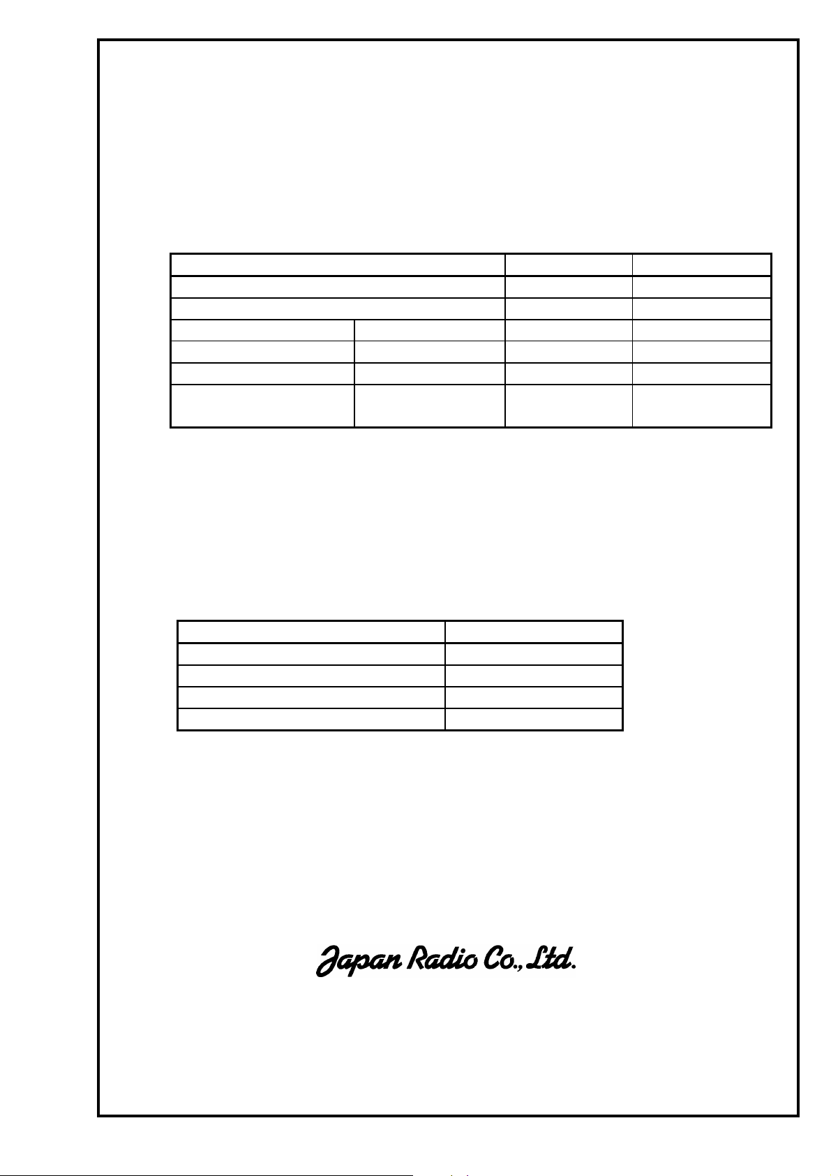
Electrical Specification: (Table 1)
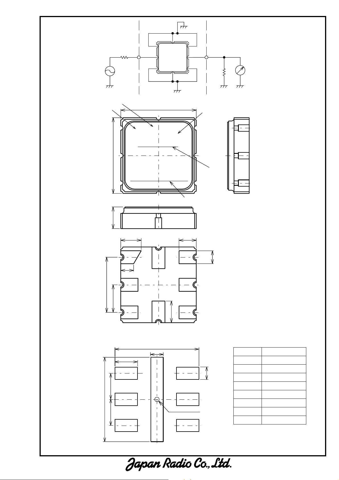
The device characteristics are measured in the circuit shown in Fig.1.
Maximum Rating: (Table 2)
Mechanical Specifications: (Fig.2)
Package is designed as small as 3.5x3.5x1.0[mm
Notice:
This part is electrostatic discharge sensitive and may be damaged by improper handling.
428MHz Low Power Transceiver
Table 1. Electrical Specifications
Item Spec. Typ.
Input and Output Impedance Nominal Center Frequency (f0) - 428MHz
Insertion Loss 426~430MHz 3.5dB max. 2.0dB
Response Variation 426~430MHz 1.5dB max. 0.4dB
Input and Output VSWR 426~430MHz 2.5 max. 1.6
Out of Band Rejection
(Relative to Through Level)
Table 2. Maximum Ratings
Item Rating
Maximum Input Power +20dBm
Maximum DC Voltage 7.5V
Operating Temperature Range -40~+85ºC
Storage Temperature -40~+85ºC
http://www.jrc.co.jp/jp/product/device/saw/index.html (Japanese)
JRC SAW FILTER
NSVS1089
383~389MHz 50dB min. 58dB
(Operating Temperature Range: -40~+85ºC)
3
] for SMD (Surface Mount Device) type.
Communications Equipment Division
Communications Equipment Marketing Department
10-1, Nishi-Shinjuku 6-chome, Shinjuku-ku,
Tokyo, 160-8328 Japan
Tel. +81 3-3348-3845
Fax. +81 3-3348-3935
http://www.jrc.co.jp/eng/product/saw/index.html(English)
50Ω
Page 2
IN
(a)
50Ω
(b)
Fig.2 Measuring circuit
3. 5±0. 2
8
SAW
7
6
1
2
345
4Y0
3. 5±0 . 2
JK
(2)
1. 0±0. 2
(0. 95)
4
3
(0. 6)
2
)
(2.54)
7
2
.
1
(
1
8
Fig.3 Package dimensions (in mm)
4.3
0.8
1.3
[6x]
1.27
4.3
1.27
Fig.4 Desirable land area (in mm)
(0. 8)
[5x]
[2x]
(1.0)
Via-Hole(Φ0.3)
NSVS1089 Nov. 2004
OUT
50Ω
(c)
(1)
Marking
(1) Lot Number
(a) Year
5
[8x]
(0.6)
6
7
0.8
[6x]
(b) Month
*Oct.--- X
Nov.--- Y
Dec.--- Z
(c) Date
1-9--- 0
10-19--- 1
20-31--- 2
(2) Part Number Mark
Pin no. Connection
1 GND
2 IN/OUT
3 GND
4 GND
5 GND
6 OUT/IN
7 GND
8 GND
Page 3
NSVS1089 Nov. 2004
Notice
1. Use this component within operating temperature range. It might not be
satisfied with electrical specification without operating temperature range.
When it is used less than -40ºC or more than +85ºC, it might be a cause of
degradation or destruction of the component. Even if it endures during a short
time, it causes degradation of qualification.
2. When soldering iron is used, solder with the temperature at the tip of soldering
iron: 350ºC max., the time of soldering: 10 seconds max., the power of
soldering iron: 30W max..
3. Notice that the allowed time of soldering with soldering iron is accumulated
time, when soldering is repeated.
4. As rapid temperature change for cleaning after reflow soldering might be a
cause of destruction clean this component after confirming that temperature of
this component goes down to room temperature.
5. Confirm that there are not any influence for qualification to this component in
mounting on PCB when this component is cleaned.
6. As it might be a cause of degradation of destruction to apply static electricity to
this component, do not apply static electricity or excessive voltage while
assembling and measuring. And do not transport this component with bare
hand.
7. As it might be a cause of degradation or destruction to apply D.C. voltage
between each terminal, apply D.C. voltage 7.5V max. in actual circuit.
Note
1. This specification specifies the quality of this component as a single unit. Make
sure that this component is evaluated and confirmed against this specification
when it is mounted to your products.
2. The information contained herein may be changed without prior notice. It is
therefore advisable to contact Japan Radio Company before proceeding with the
design of equipment incorporating this product.
3. The products are designed to be used with ordinary electronic equipment (data
and communications equipment, office equipment, audio-video equipment,
measuring instruments, etc). Japan Radio Company does not assume any
liability for the case using the products with the application required high
reliability or safety extremely (such as space equipment, sea-bottom equipment,
medical equipment etc). When intending to use any our product please
contact our sales representatives in advance.
Page 4
NSVS1089 Nov. 2004
Fig.1 Measuring circuit
(R0.3)
[4
×]
(1.4)
(0.8 )
[12×]
Pin No. Connection
1GND(PKG)
2GND(PKG)
3 GND(PKG)
4GND(PKG)
5OUT/IN
6 GND(signal)
7GND(PKG)
8GND(PKG)
9GND(PKG)
10 GND(PKG )
11 IN/OUT
12 GND(signal)
(b)
(3)
Marking
(1) Manufacture's Mark
(2) Lot Number
(a) Year
(b) Month
*Oct.--- X
Nov.--- Y
Dec.--- Z
(c) D a te
1-9 --- 0
10 -19--- 1
20 -31--- 2
(3) Part Number Mark
(1.26± 0.1 3)
[12× ]
[12× ]
(2.5 4 )
(R0.3)
(2)
4
5
6
7
8
910
(C)
1234
10
987
11
12
6
5
OUT
50O
SAW
*27nH
*27nH
39pF
33pF
*murata LQ W 18A series
S21
0
FREQUENCY CHARACTERISTICS
0
Insertion Loss [dB]
11 11
9 9
7 7
5 5
VSWR
3 3
1 1
InsertionLoss [dB]
20
40
60
80
100
CH1 : center 428 span 100
CH2 : center 428 span 100
S11 S22
S11 S22
378 378 478 478
S21
0
20
40
60
80
100
0.3 3000
VSWR
Frequency [MHz] Frequency [MHz]
Frequency [MHz]
2
4
6
8
10
Insertion Loss [dB]
 Loading...