


JRC NJW1104FC2-80, NJW1104FC2 Datasheet
DOLBY PRO LOGIC SURROUND DECODER
DATA
SCK
REQ
AUX1
10
MD1
MD2
NJW1104
PPRELIMINARY
GENERAL DESCRIPTION
nnnn
NJW1104
The
is a surround processor including all of
the necessary circuits of Dolby Pro Logic Surround
decoder and digital delay.
In addition to Dolby Pro Logic Surround function, it
performs easily other surround f unction such as Hall, Live,
Disco and others.
Dolby and double-D symbol are trademarks of Dolby Laboratories Licensing Corporation.
San Francisco, CA94103-4813.US A.
This device is available only t o l i censees of Dolby Lab.
Licensing and application information may be obtained from Dolby Lab.
FEATURES
nnnn
l Operating Voltage : V
=10V(Analog Block), VDD=5V(Digital Block)
CC
l Digital Delay on chip
l Serial Data Interface(3-wire) DATA, REQ, SCK
l Bi-CMOS Technology
l Package Outline QFP80, QFP100
FUNCTION
nnnn
[Dolby Pro Logic Surround]
l Automatic input balance
l Noise sequencer
l Adaptive matrix
l Center channel control
(Wide band, Normal, Phantom, Off)
l Modified B-type noise reduction
l 7kHz low-pass filter
l Dolby 3 stereo mode
l Digital time delay(15,20,25,30msec.)
PACKAGE OUTLINE
nnnn
NJW1104FC2-80 NJW1104FC2
[Other Surround]
l Surround Signal Selector
(L+R, L-R, EXTIN)
l Front mixing control
l Digital time delay
(15,20,25,30,40,50,60msec.)
[Other Function]
l Digital auxiliary outputs
(AUX1-AUX10)
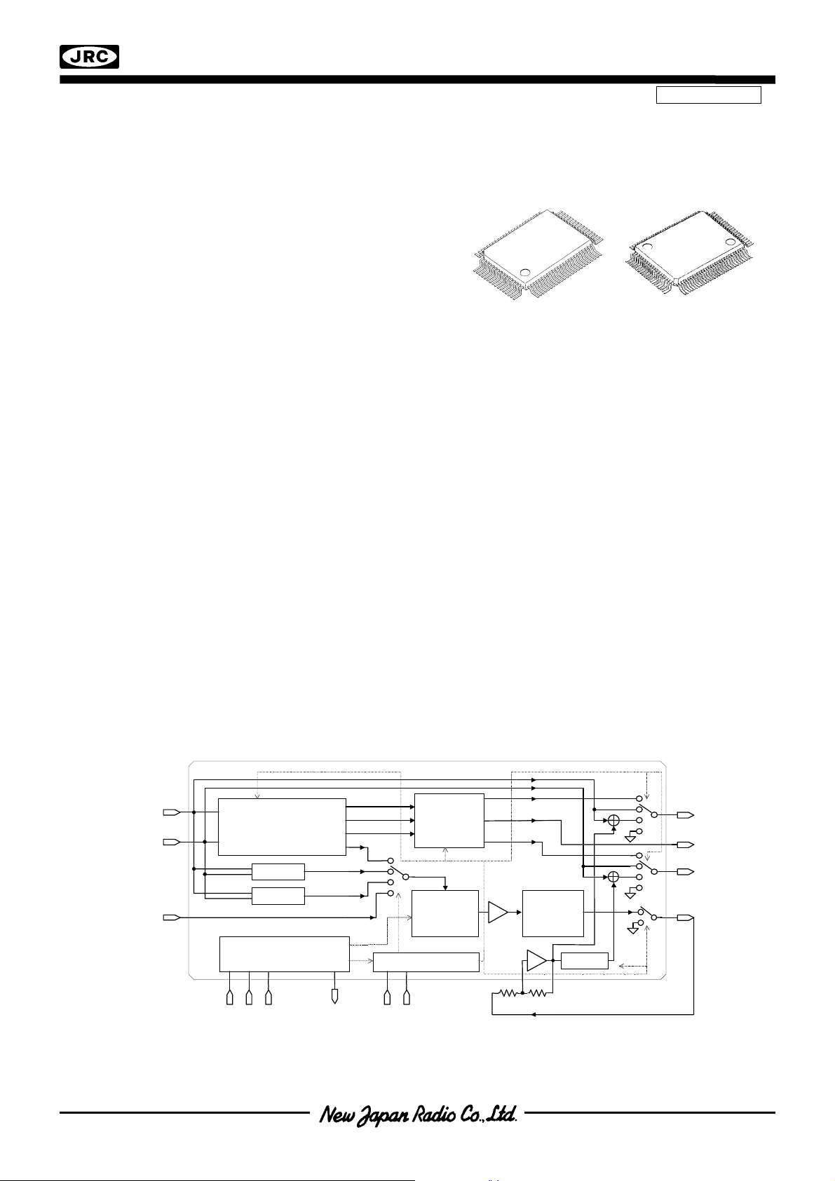
SYSTEM BLOCK DIAGRAM
nnnn
LIN
RIN
EXTIN
Input Autobalance
Noise Sequencer
Adaptive Matrix
L+R
L-R
MCU Interface
Center Mode
7KHz
LPF
Modified
B-NR
ADD/SUB
.
Delay
SW. Controller
-
LOUT
COUT
ROUT
SOUT
Ver.1.0
- 1 -
NJW1104
ABSOLUTE MAXIMUM RATING (Ta=25°C)
nnnn
PARAMETER
Supply Voltage
Power Dissipation
Operating Temperature Range
Storage Temperature Range
*
SYMBOL
V
CC
V
DD
P
D
T
opr
T
stg
RATING
13
6.5
(QFP80) 1.3
(QFP100) 1.3
-20 to +75
-40 to +125
UNIT
V
W
°C
°C
*On board
ELECTRICAL CHARACTERISTICS (V
nnnn
PARAMETER SYMBOL TEST CONDITION MIN. TYP. MAX. UNIT
OVERALL
u
Supply Voltage Range V
Supply Current I
Reference Voltage V
Threshold Voltage V
INPUT AUTO BALANCE
u
Capture Range CPR - 5 -
Error Correction CER - 4 -
ADAPTIVE MATRIX (0dB=300mVrms, f=1kHz at Cin Cout)
u
Output Level Accuracy
relative to Cch
Matrix Rejection relative MR L,R,S’ch.out 25 40 - dB
Headroom HR-AM VCC=9V at THD=1% 15 17 - dB
Total Harmonic Distortio n THD-AM L,R,C,S’ch.out at 4ch.mode
Signal to Noise Ratio SNAM Rg=0,wt:CCIR-ARM at 4ch.mode
NOISE SEQUENCER
u
Output Noise Level Vno -15.0 -12.5 -10.0 dB
Output Noise Level
Accuracy relative to Cch
MODIFIED B-TYPE NOISE REDUCTION (0dB=300mVrms, f=100Hz at Sin Sout)
u
Voltage Gain GV-NR Vin=0dBd,f=100Hz - 9.5 - dB
Decode Responce1 DEC1 Vin=0dBd,f=1kHz -1.6 -0.1 1.4 dB
Decode Responce2 DEC2 Vin=-15dBd,f=1.4kHz -3.0 -1.5 0.0 dB
Decode Responce3 DEC3 Vin=-20dBd,f=1.4kHz -4.9 -3.4 -1.9 dB
Decode Responce4 DEC4 Vin=-40dBd,f=5kHz -6.8 -5.3 -3.8 dB
Total Harmonic Distortion THDNR Vin=0dBd,f=1kHz - 0.07 0.3 %
Headroom HRNR VCC=9V at THD=1% 15 17 - dB
Signal to Noise Ratio SNNR Rg=0,weightted:CCIR/ARM 73 78 - dB
=10V, VDD=5V, Ta=25°C)
CC
4.5
0.7V
0.0
9
-
-
DD
CC
V
DD
CC
I
DD
REF
thh
V
Vol L,R,S’ch.out -0.5 0 0.5 dB
D
No Signal
No Signal
No Signal 3.6 4.0 4.4 V
Digital input high level
Digital input low level
thl
-
L,R,ch.out at 2ch.mode
-
75
L,R,ch.out at 2ch.mode
Vno L,R,S’ch.out -0.5 0.0 0.5 dB
D
93
10
5
37
6
-
-
0.05
0.002
80
100
13
5.5
50
10
V
0.3V
0.2
0.1
DD
DD
-
-
V
V
mA
mA
V
V
%
%
dB
dB
Ver.1.0
- 2 -