

DOLBY PRO LOGIC SURROUND DECODER
DATA
SCK
REQ
AUX1
10
MD1
MD2
NJW1104
PPRELIMINARY
GENERAL DESCRIPTION
nnnn
NJW1104
The
is a surround processor including all of
the necessary circuits of Dolby Pro Logic Surround
decoder and digital delay.
In addition to Dolby Pro Logic Surround function, it
performs easily other surround f unction such as Hall, Live,
Disco and others.
Dolby and double-D symbol are trademarks of Dolby Laboratories Licensing Corporation.
San Francisco, CA94103-4813.US A.
This device is available only t o l i censees of Dolby Lab.
Licensing and application information may be obtained from Dolby Lab.
FEATURES
nnnn
l Operating Voltage : V
=10V(Analog Block), VDD=5V(Digital Block)
CC
l Digital Delay on chip
l Serial Data Interface(3-wire) DATA, REQ, SCK
l Bi-CMOS Technology
l Package Outline QFP80, QFP100
FUNCTION
nnnn
[Dolby Pro Logic Surround]
l Automatic input balance
l Noise sequencer
l Adaptive matrix
l Center channel control
(Wide band, Normal, Phantom, Off)
l Modified B-type noise reduction
l 7kHz low-pass filter
l Dolby 3 stereo mode
l Digital time delay(15,20,25,30msec.)
PACKAGE OUTLINE
nnnn
NJW1104FC2-80 NJW1104FC2
[Other Surround]
l Surround Signal Selector
(L+R, L-R, EXTIN)
l Front mixing control
l Digital time delay
(15,20,25,30,40,50,60msec.)
[Other Function]
l Digital auxiliary outputs
(AUX1-AUX10)
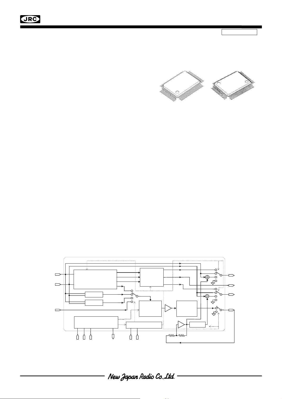
SYSTEM BLOCK DIAGRAM
nnnn
LIN
RIN
EXTIN
Input Autobalance
Noise Sequencer
Adaptive Matrix
L+R
L-R
MCU Interface
Center Mode
7KHz
LPF
Modified
B-NR
ADD/SUB
.
Delay
SW. Controller
-
LOUT
COUT
ROUT
SOUT
Ver.1.0
- 1 -
NJW1104
ABSOLUTE MAXIMUM RATING (Ta=25°C)
nnnn
PARAMETER
Supply Voltage
Power Dissipation
Operating Temperature Range
Storage Temperature Range
*
SYMBOL
V
CC
V
DD
P
D
T
opr
T
stg
RATING
13
6.5
(QFP80) 1.3
(QFP100) 1.3
-20 to +75
-40 to +125
UNIT
V
W
°C
°C
*On board
ELECTRICAL CHARACTERISTICS (V
nnnn
PARAMETER SYMBOL TEST CONDITION MIN. TYP. MAX. UNIT
OVERALL
u
Supply Voltage Range V
Supply Current I
Reference Voltage V
Threshold Voltage V
INPUT AUTO BALANCE
u
Capture Range CPR - 5 -
Error Correction CER - 4 -
ADAPTIVE MATRIX (0dB=300mVrms, f=1kHz at Cin Cout)
u
Output Level Accuracy
relative to Cch
Matrix Rejection relative MR L,R,S’ch.out 25 40 - dB
Headroom HR-AM VCC=9V at THD=1% 15 17 - dB
Total Harmonic Distortio n THD-AM L,R,C,S’ch.out at 4ch.mode
Signal to Noise Ratio SNAM Rg=0,wt:CCIR-ARM at 4ch.mode
NOISE SEQUENCER
u
Output Noise Level Vno -15.0 -12.5 -10.0 dB
Output Noise Level
Accuracy relative to Cch
MODIFIED B-TYPE NOISE REDUCTION (0dB=300mVrms, f=100Hz at Sin Sout)
u
Voltage Gain GV-NR Vin=0dBd,f=100Hz - 9.5 - dB
Decode Responce1 DEC1 Vin=0dBd,f=1kHz -1.6 -0.1 1.4 dB
Decode Responce2 DEC2 Vin=-15dBd,f=1.4kHz -3.0 -1.5 0.0 dB
Decode Responce3 DEC3 Vin=-20dBd,f=1.4kHz -4.9 -3.4 -1.9 dB
Decode Responce4 DEC4 Vin=-40dBd,f=5kHz -6.8 -5.3 -3.8 dB
Total Harmonic Distortion THDNR Vin=0dBd,f=1kHz - 0.07 0.3 %
Headroom HRNR VCC=9V at THD=1% 15 17 - dB
Signal to Noise Ratio SNNR Rg=0,weightted:CCIR/ARM 73 78 - dB
=10V, VDD=5V, Ta=25°C)
CC
4.5
0.7V
0.0
9
-
-
DD
CC
V
DD
CC
I
DD
REF
thh
V
Vol L,R,S’ch.out -0.5 0 0.5 dB
D
No Signal
No Signal
No Signal 3.6 4.0 4.4 V
Digital input high level
Digital input low level
thl
-
L,R,ch.out at 2ch.mode
-
75
L,R,ch.out at 2ch.mode
Vno L,R,S’ch.out -0.5 0.0 0.5 dB
D
93
10
5
37
6
-
-
0.05
0.002
80
100
13
5.5
50
10
V
0.3V
0.2
0.1
DD
DD
-
-
V
V
mA
mA
V
V
%
%
dB
dB
Ver.1.0
- 2 -

NJW1104
ELECTRICAL CHARACTERISTICS (V
nnnn
PARAMETER SYMBOL TEST CONDITION MIN. TYP. MAX. UNIT
OTHER SURROUND
u
Total Harmonic Distortion THDOS Vin=0dBd,f=1kHz
Headroom HROS VCC=9V at THD=1%
Signal to Noise Ratio SNOS Rg=0,weighted:CCIR/ARM
DIGITAL TIME DELAY
u
Delay Time Td f
Total Gain Gv -3.0 0.0 3.0 dB
Total Harmonic Distortion THD Vin=0.3Vrms
Maximum Output Voltage Vomax Vin:f=1kHz
Output Noise Voltage No Rg=600
DIGITAL AUXILIARY OUTPUT
u
Low Level Output VOL Output Current=-1mA 0.0 - 0.3V
High Level Output VOH Output Current=1mA 0.7V
=10V, VDD=5V, Ta=25°C)
CC
L+R,L-R output
L+R,L-R mode
L+R,L-R mode
=4MHz
OSC
Td=15.4ms - 0.3 0.6 %
f=1kHz
30kHz LPF
30kHz LPF,THD=3%
W
Vin=0Vrms
JIS-A
Td=20.5ms - 0.3 0.6 %
Td=25.6ms - 0.4 0.8 %
Td=30.7ms - 0.5 1.0 %
Td=41.0ms - 0.6 1.2 %
Td=51.2ms - 0.7 1.4 %
Td=61.4ms - 0.8 1.6 %
Td=15.4ms - -85 -75 dBV
Td=20.5ms - -85 -75 dBV
Td=25.6ms - -85 -75 dBV
Td=30.7ms - -80 -70 dBV
Td=41.0ms - -80 -70 dBV
Td=51.2ms - -80 -70 dBV
Td=61.4ms - -75 -65 dBV
- 0.05 0.2 dB
15 17 - dB
75 80 - dB
12.4 15.4 18.4 ms
17.5 20.5 23.5 ms
22.6 25.6 28.6 ms
27.7 30.7 33.7 ms
38.0 41.0 44.0 ms
48.2 51.2 54.2 ms
58.4 61.4 64.4 ms
1.5 1.8 - Vrms
DD
DD
-VDDdB
dB
Ver.1.0
- 3 -

NJW1104
0
4
0
3
4
3
0
1
0
1
0
1
1
1
PACKAGE OUTLINE (QFP100-C2)
nnnn
80
23.9
20.0
±0.
±0.
51
0 - 10°
5081
.
.
±
±
17.9
14.0
.
±
0.15
PIN CONNECTION
nnnn
Pin No. Pin Name Pin No. Pin Name Pin No. Pin Nam e Pin No. Pin Name
1RLC326NC51NC76DBIN
2RLC827NC52NC77DBC1
3RLC628NC53NC78DBC2
4 LLI 29 NC 54 NC 79 DBC3
5 LBPF 30 NC 55 NC 80 LOUT
6 RLI 31 VSS 56 NC 81 ROUT
7 RBPF 32 AUX1 57 NC 82 COUT
8LT33AUX258NC83SOUT
9RT34AUX359NC84CMC
10 LIN 35 AUX4 60 NC 85 SMRO
11 RIN 36 AUX5 61 NC 86 SMRI
12 HOLDC 37 AUX6 62 VDD 87 EXTIN
13 NGC3 38 AUX7 63 VCC 88 VREF
14 NGC2 39 AUX8 64 SDOUT 89 IREF
15 NGC1 40 AUX9 65 LPF1IN 90 PSC3
16 GND 41 AUX10 66 LPF1OUT 91 PSC6
17 MD1 42 RST 67 OPA1IN 92 PSC2
18 MD2 43 TESTCNT 68 OPA1OUT 93 PSC5
19 VSS 44 DATA 69 CC1 94 PSC1
20 NC 45 SCK 70 CC2 95 PSC4
21 NC 46 REQ 71 OPA2IN 96 RLC5
22 NC 47 CLK2 72 OPA2OUT 97 RLC2
23 NC 48 CLK1 73 LPF2IN 98 RLC1
24 NC 49 VDD 74 LPF2OUT 99 RLC4
25 NC 50 NC 75 LPFIN 100 RLC7
0.8
1
±0.
0.65
0.30
±0.
30
0.12 M
31100
0.15
MAX
3.0
.
±
.
±
2.7
0.1
Ver.1.0
- 4 -

PACKAGE OUTLINE (QFP80-C2)
0
4
0
3
4
3
0
1
0
1
0
1
1
1
nnnn
23.9
20.0
NJW1104
0 - 10°
±0.
±0.
.
±
0.15
65
64
124
0.8
0.35
±0.
41
0.12 M
40
2580
.
±
14.0
MAX
3.0
.
±
17.9
.
±
2.7
PIN CONNECTION
nnnn
Pin No. Pin Name Pin No. Pin Name Pin No. Pin Nam e Pin No. Pin Name
1 MD2 21 NC 41 DBC3 61 RLC4
2 MD2 22 VDD 42 LOUT 62 RLC7
3 VSS 23 VCC 43 ROUT 63 RLC3
4 AUX1 24 VCC 44 COUT 64 RLC8
5 AUX2 25 SDOUT 45 SOUT 65 RLC6
6 AUX3 26 SDOUT 46 CMC 66 LLI
7 AUX4 27 LPF1IN 47 SMRO 67 LBPF
8 AUX5 28 LPF1OUT 48 SMRI 68 RLI
9 AUX6 29 OP1IN 49 EXTIN 6 9 RBPF
10 AUX7 30 OP1OUT 50 VREF 70 LT
11 AUX8 31 CC1 51 IREF 71 RT
12 AUX9 32 CC2 52 PSC3 72 LIN
13 AUX10 33 OP2IN 53 PSC6 73 RIN
14 RST 34 OP2OUT 54 PSC2 74 HOLDC
15 TESTCNT 35 LPF2IN 55 PSC5 75 NGC3
16 DATA 36 LPF2OUT 56 PSC1 76 NGC2
17 SCK 37 LPFIN 57 PSC4 77 NGC1
18 REQ 38 DBIN 58 RLC5 78 GND
19 CLK2 39 DBC1 59 RLC2 79 MD1
20 CLK1 40 DBC2 60 RLC1 80 MD1
0.8
±0.
0.15
.
±
0.1
Ver.1.0
- 5 -

NJW1104
Ver.1.0
- 6 -
[CAUTION]
The specifications on this databook are only
given for information , without any guarantee
as regards either mistakes or omissions. The
application circuits in this databook are
described only to show representative usages
of the product and not intended for the
guarantee or permission of any right including
the industrial rights.
 Loading...