

NJU8402
PRELIMINARY
DIGITAL TO ANALOG CONVERTER
FOR STEREO AUDIO
GENERAL DESCRIPTION
■
NJU8402
The
Converter for stereo audio. It cons ists of Ser ial A ud io Da ta
Interface, Digital Interpolation Filter, ∆Σ Modulator, SC LPF ,
Buffer Amp, System Controller for status control. It
operates on single +5V power supply. Furthermore, it
accepts 16-bit input audio data length or 18-bit, and
supports I
Therefore, the
and other digital audio applications.
FEATURES
■
●
∆Σ type 1bit stereo DAC
●
Sample Rate ( fs ) : 50kHz ( Maximum )
●
Signal-to-Noise Ratio : 94dB
●
Input Audio Data Length : 16bits or 18bits
●
Single ended Analog Output
●
Internal SC type Low Pass Filter
●
Operating Voltage +5V ±5%
●
Package Outline DIP16 / DMP16
is a 16-bit delta-sigma Digital-to-Analog
2
S serial data format and LSB justified.
NJU8402
is suitable for CD, MD, DAT
PACKAGE OUTLINE
■
NJU8402D NJU8402M
PIN CONFIGURATION
■
V
MCKI
SCK
DATA
REQ
AOUTL
VCOML
AV
1
DD
2
3
4
5
6
7
89
DD
16
15
14
13
12
11
10
V
SS
BCLK
LRCK
DIN
RST
AOUTR
VCOM
AV
SS
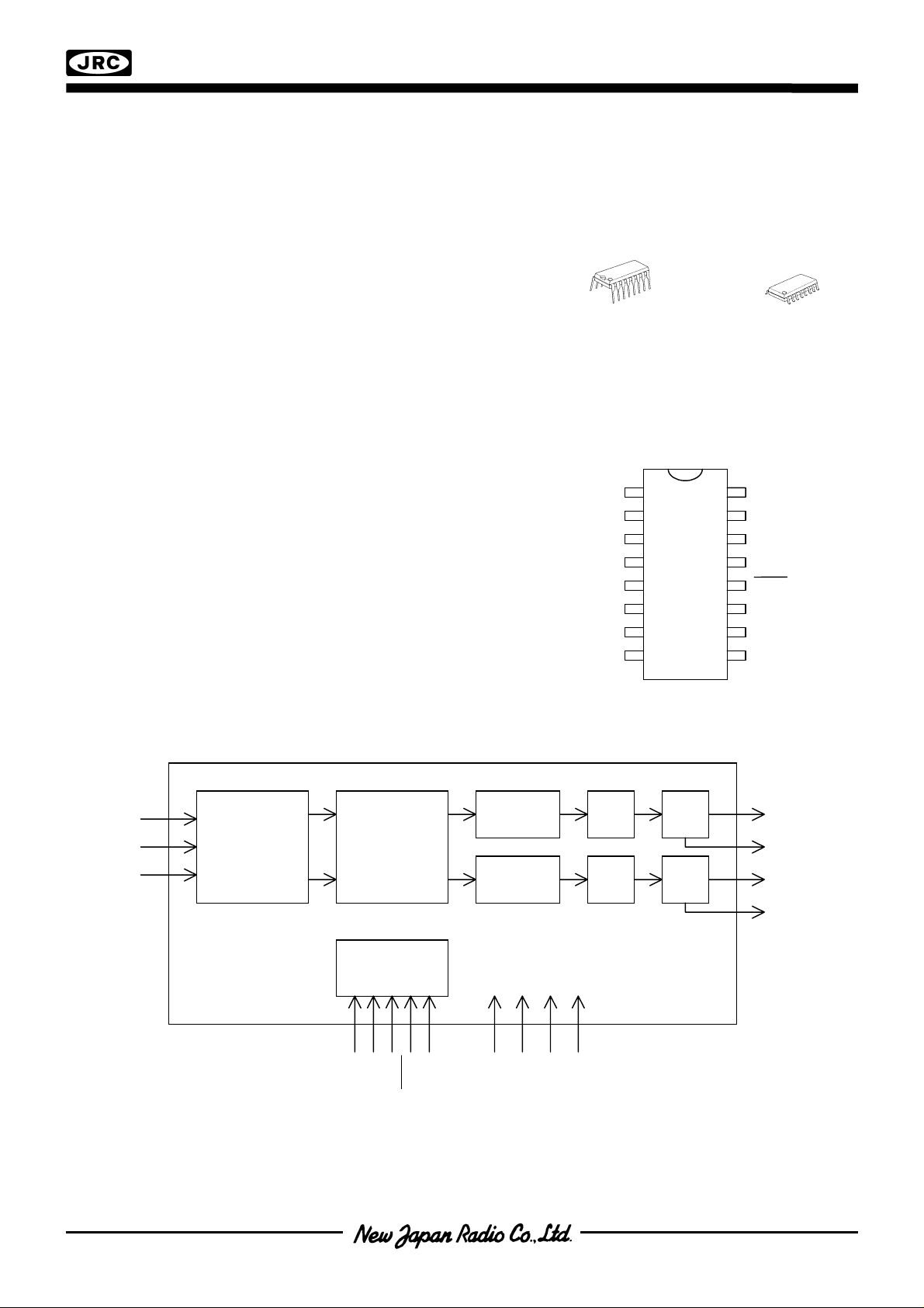
BLOCK DIAGRAM
■
DIN
BCLK
LRCK
Serial Audio
Data Interface
Digital
Interpolation
Filter
System
Controller
REQ
MCKI
RST
SCK
DD
AV
SS
AV
SC
LPF
SC
LPF
LPF
LPF
AOUTL
VCOML
AOUTR
VCOMR
∆Σ
Modulator
∆Σ
Modulator
SS
DD
V
DATA
V
- 1 -
NJU8402
TERMINAL DESCRIPTION
■
PIN
SYMBOL
No.
1V
16 V
8AV
9AV
DD
SS
DD
SS
INPUT
/OUTPUT
FUNCTION
Digital Power Supply, +5V
Digital GND, 0V
Analog Power Supply, +5V
Analog GND, 0V
2 MCKI I Master Clock Input Terminal
The input signal frequency is 256 times or 384 times of fs.
13 DIN I Serial Audio Data Input Terminal
14 LRCK I
15 BCLK I
L/R Channel Clock Input Terminal
This clock must synchronize with MCKI.
Audio Serial Data Clock Input Terminal
This clock must synchronize with MCKI.
Control Register Serial Data Sift Clock Input Terminal
3SCK I
Control register leads the control data synchronizing the rising edge of SCK
signal. When the c ontrol register is not used, the state of SCK terminal h as to
keep level ”H”.
Control Register Serial Data Input Terminal
4DATA I
Input data sets various functions.
When the control register is not used, the state of DATA terminal has to keep level
“H”.
Control Register Serial Data Request Input Terminal
The control data are latched in the control register at the rising edge of REQ
5REQ I
signal.
When the control re gist er is not us ed, the s t ate of REQ terminal has to keep level
“H”.
12 RST I
Reset
“L” level signal into reset terminal initializes the system.
Left channel Analog Signal Common Terminal for Connecting Smooth Capacitor
7VCOML
A chemical capacitor should be connected between this terminal and AVSS for
stabilizing.
Right Channel Analog Signal Common T erminal for Connecting Smooth Capacitor
10 VCOMR
A chemical capacitor should be connected between this terminal and AVSS for
stabilizing.
6 AOUTL O L-Channel Analog Signal Output Terminal
11 AOUTR O R- Chann el An al og Sig na l Output Terminal
- 2 -
FUNCTION DESCRIPTION
■
(1-1) Analog Audio Signal Output
Analog signal output is biased in the chip and the maximum amplitude is 0.56 × AV
switched capacitor Low Pass Filter is so effective that the ex ternal Low Pass Filters are requir ed only 2pole LPF or 3-pole.
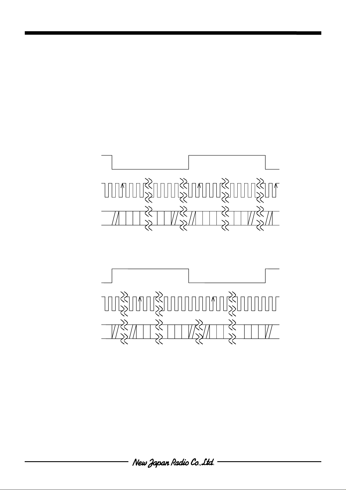
(1-2) Serial Data Interface
DIN (Data Input), BCLK (Bit Clock) and LRCK (L/R Clock) are the serial data interface terminals. BCLK is
the bit clock of audio data and IO data are leaded at raising edge of the BCLK. The signa l into LRCK
terminal represents the signal for distinguishing between Lch and Rch, and the signal for starting data. The
frequency of LRCK is s ampling rate of s ystem ( fs ). The MCIK m ust be synchronized with LRCK and is
256 times or 384 of fs. The s erial data f orm at is com plem ent of 2, MSB-f irs t and compatib le with I
data protocol or LSB justified. This serial data format is set by the control register.
NJU8402
. The internal
DD
2
S serial
LRCK
BCLK
DIN
LRCK
BCLK
Left
151413 10 151413 10
2
S serial data format
I
Left
Right Channel
Right Channel
DIN
(1-3) System Clock
System Clock into the MCIK terminal must be 256 times or 384 times of fs and synchronizing with LRCK.
This frequency is set by the control register.
(1-4) Reset
The external reset is the asynchronous reset. Reset is released at the f alling edge at LRC K. Reset by
command is synchronous which operates as same as the external reset function.
15140 10 15142 10
LSB justified serial data format
2
- 3 -

NJU8402
(1-5) Control Register
The Control Register controls
sift clock, the REQ term inal is data request sig nal, the DATA terminal is the seria l data input. The co ntrol
data is loaded into the sift r egister at risi ng edge of SCK, then it is latched at t he rising edg e of REQ. The
least 8-bit data, which order is MSB first, is valid for control.
NJU8402
REQ
SCK
DATA B7 B6 B5 B4 B3 B2 B1 B0
operation using the serial interface. The SCK terminal is the data
CONTROL PORT TIMING CHART
•
Serial Data Format
B7 B6 B5 B4 B3 B2 B1 B0
0000
0001
System Clock CLKR 256fs 384fs 0
Data Length DIF0 16 18 0
Format DIF1 I2S LSB Justified 0
Reset RST Normal Reset *2
∗
∗∗∗
*1 Don't input commands except this table.
0 1 Default
*2 The level becomes 0 after initial setting.
DIF1 DIF0 CLKR
RST
(∗: Don’t Care)
- 4 -

ABSOLUTE MAXIMUM RATING
■
PARAMETER SYMBOL CONDITIONS UNIT
NJU8402
(VSS=AVSS=0V)
Power Supply
DIGITAL V
ANALOG AV
- A V
V
DD
DD
DD
DD
∆VAVD V
Input Voltage VIN
Operating Temperature Ta
Storage Temperature Tstg
Power Consumption PD
RECOMMENDATION OPERATION CONDITION
■
PARAMETER SYMBOL
Power
Supply
DIGITAL V
ANALOG AV
DD
DD
−0.3 to+7.0
−0.3 to +7.0
DD
+ 0.3
DD
<0.2
- A V
DD
−0.3 to V
−30 to +80 °C
−40 to +125 °C
500(DIP16)
mW
200(DMP16)
(VSS=AVSS=0V)
CONDITIONS
MIN. TYP. MAX.
UNIT
4.75 5.0 5.25 V
4.75 5.0 5.25 V
V
V
V
V
- 5 -

NJU8402
p
ELECTRICAL CHARAC TERISTICS
■
ANALOG AC CHARACT ERI STI CS
•
(The case without the report Ta=25℃,VDD=AVDD=5.0V,fs=44.1kHz, Input Signal Frequency=1kHz,
Input Signal Level=Full Scale,MCKI=256fs,Bandwidth=22Hz to 20kHz)
PARAMETER SYMBOL CONDITIONS MIN. TYP. MAX. UNIT NOTE
Resolution
S/N S/N EIAJ, A-we igh t 90 94
Dynamic Range DR EIAJ, A-weight
THD+N THD+N Output 0dB
Channel Separation EIAJ(1kHz)
Differential Gain
Between Channels
Gain Drift
Maximum Output Voltage
Bias
Output Load Resistance 10
Output Load Capacitance
−88 −82
0.55×AV
DD
0.50×AV
16
94
90
0.1 0.3 dB
100
0.57×AVDD0.59×AV
DD
kΩ
300 pF
DD
bit
dB
dB
dB
dB
ppm/°C
V
PP
V
BLOCK DIAGRAM FOR TESTING ANALOG AC CHARACTERISTICS
Digital
Digital
Data
Audio
Interface
Receiver
Chi
NJU8402 Evaluation Board Audio Analyzer
Two-pole LPF : fc=25kHz ( refer ■APPLICATION CIRCUITS )
Filters : 22Hz HPF + 20kHz Ten-pole LPF
NJU8402
( A-Weighting Filter is on at measuring S/N and Dynamic Range )
Two-pole
LPF
Filters
THD
Meter
- 6 -

DIGITAL INTERPOLATION FILTER CHARACTERISTICS
•
(The case without the report. Ta=25℃,VDD=AVDD=5.0V ,fs=44.1kHz)
PARAMETER SYMBOL CONDITIONS MIN. TYP. MAX. UNIT NOTE
Band Pass PB 0.02
Rejection Band SB 24.10
Rejection Band Quantity SA 50
Note :Band Pass and Rejection Band are proportioned to fs. PB=0.4535×fs,SB=0.5465×fs
DIGITAL ANALOG LOW PASS FILTER CHARACTERISTIC
•
(The case without the report. Ta=25℃,VDD=AVDD=5.0V ,fs=44.1kHz)
PARAMETER SYMBOL CONDITIONS MIN. TYP. MAX. UNIT NOTE
Frequency Response FR
POWER CHARACTERISTICS
•
22Hz~20kHz
±0.2
(The case without the report Ta=25℃,VDD=AVDD=5.0V,fs=44.1kHz)
PARAMETER SYMBOL CONDITIONS MIN. TYP. MAX. UNIT NOTE
Supply Voltage VDD, AV
Supply Current
V
AV
DD
DD
AI
I
DD
DD
DD
No signal
No signal
4.75 5.0 5.25 V
12 14 mA
10 18 mA
NJU8402
20.0 kHz
kHz
dB
dB
DIGITAL DC CHARACTERISTICS
•
PARAMETER SYMBOL CONDITIONS MIN. TYP. MAX. UNIT NOTE
V
Digital Input Voltage
Input Leakage Current I
IH
V
IL
LK
(The case without the report Ta=25℃,VDD=AVDD=5.0V)
0.7 V
DD
――±1
― V
―
0.3 V
DD
DD
V
V
µA
- 7 -

NJU8402
DIG I TAL AC CHAR ACTE R I S TICS
•
(The case without the report Ta=25℃,VDD=AVDD=5.0V)
Master Clock & Reset
PARAMETER SYMBOL CONDITIONS MIN. TYP. MAX. UNIT NOTE
Frequency f
MCKI
Pulse Width High-Level t
Pulse Width Low-Level t
Reset Low Level Width t
MCKI
MCKH
MCKL
RST
Digital Audio Signal Interface
PARAMETER SYMBOL CONDITIONS MIN. TYP. MAX. UNIT NOTE
Audio DAC Sampling Late fs 24
Audio Data Setup Time t
Audio Data Hold Time t
BLCK Period t
BLCK Pulse Time “H” t
BLCK Pulse Time “L” t
BCLK Rise to LRCK Edge
LRCK Edge to BCLK Rise t
DS
DH
BCLK
BCKH
BCKL
t
BLR
LRB
256fs 1.024
386fs 9.216 ― 19.2 MHz
12.8 MHz
50 kHz
20
20
1
50
50
1/(128fs)
20
―
――
――
――
―
――ns
――ns
――
――ns
20 ――ns
40
――
40 ――ns
ns
ns
ns
ns
ns
Control Register Interface
PARAMETER SYMBOL CONDITIONS MIN. TYP. MAX. UNIT NOTE
SCK Period t
SCK Pulse Time “H” t
SCK Pulse Time “L” t
Control Data Setup Time t
Control Data Hold Time t
REQ Pulse Time “H” t
SCK Data Setup Time
REQ Hold Time t
Input Signal Rise and Fall Time
PARAMETER SYMBOL CONDITIONS MIN. TYP. MAX. UNIT NOTE
Input Signal Rise Time
Input Signal Fall Time t
SCK
SCH
SCL
DAS
DAH
REH
t
RQS
RQH
t
UP
DN
2 ――ns
0.8
0.8
0.8
0.8
1.6
――ns
――
ns
――ns
――ns
――
ns
0.8 ――ns
0.8 ――ns
――
――
100 ns
100 ns
- 8 -

TIMING CHART
SC
•
Master Clock & Reset
MCKI
1/f
NJU8402
MCKI
RSTX
Digital Audio Signal Interface
BCLK INPUT
LRCK INPUT
DIN
t
BLR
t
LRB
t
DS
t
DH
t
MCKL
t
t
RST
BCKL
t
t
MCKH
BCLK
t
BCKH
Control Register Interface
t
RQS
REQ
t
SCH
SCK
t
K
DATA
t
DAS
Input Signal Rise and Fall Time
t
UP
t
t
SCL
DAH
t
LRD0
t
t
RQH
REH
90%
10%
t
DN
- 9 -

NJU8402
APPLICATION CIRCUITS
■
Digital Audio
Data
(16 or 18 bits)
MCK
&
8 bits
Serial Control
DIN
LRCK
BCLK
NJU8402
SCK
REQ
MCKI
RSTX
DATA
AOUTL
VCOML
AOUTR
VCOMR
AVDD
AVSS
VDD
VSS
Two-pole LPF
2.2uF
OP:NJM5532
10uF
10uF
10uF
10uF
20kΩ
20kΩ
680pF
150pF
20kΩ
Two-pole LPF
(+5V)
AV
DD
0.1uF
VDD (+5V)
0.1uF
+12
10uF
OP
10uF
-12V
AVSS (Analog GND)
VSS (Digital GND)
0.1uF
0.1uF
- 10 -
[CAUTION]
The specifications on this databook are only
given for information , without any guarantee
as regards either mistakes or omissions. The
application circuits in this databook are
described only to show representative usages
of the product and not intended for the
guarantee or permission of any right including
the industrial rights.
 Loading...