

3
412
L
LOW DROPOUT VOL TAGE REGULA T OR
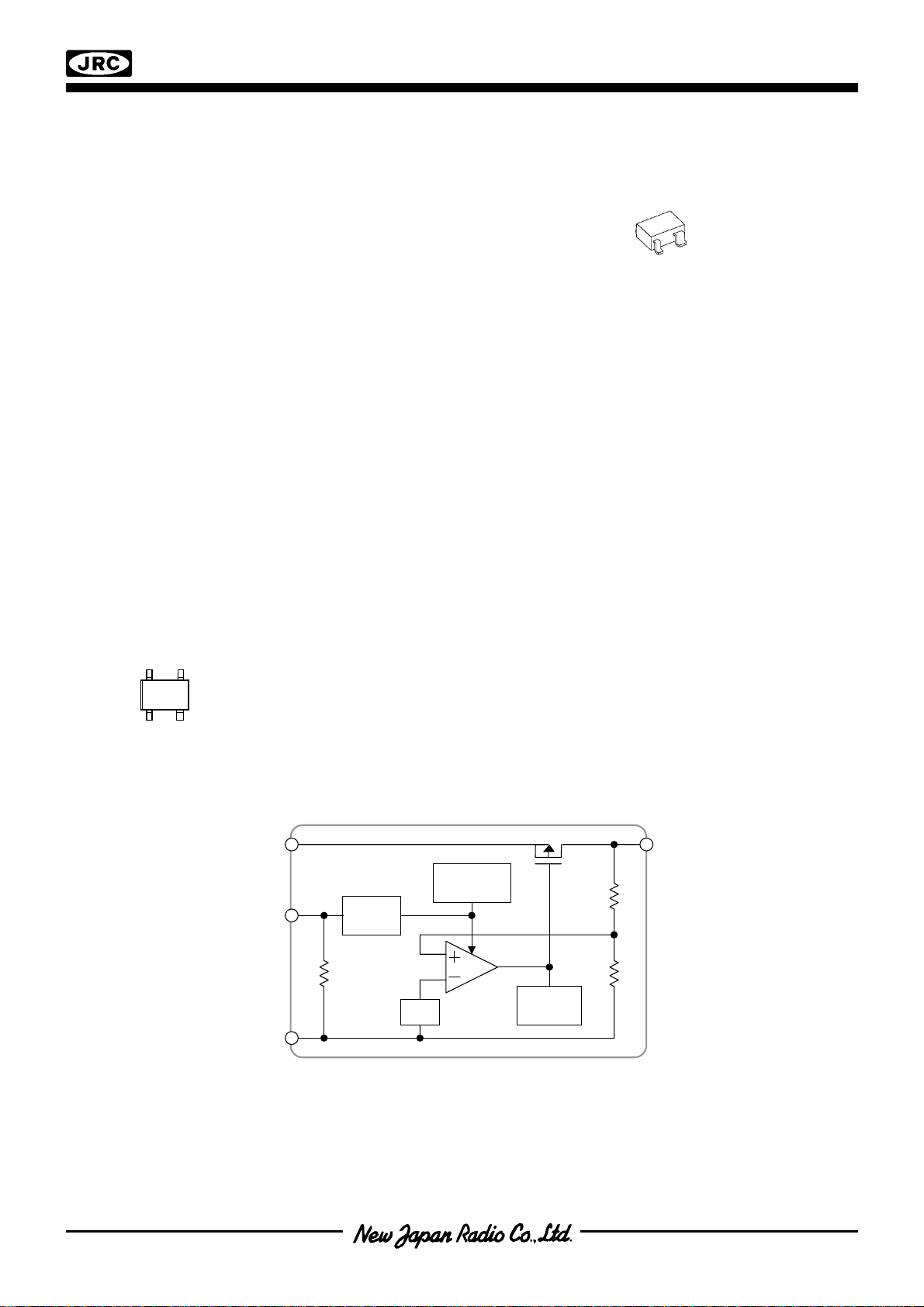
GENERAL DESCRIPTION PACKAGE OUTLINE
The NJU7777 is a 150mA output low dropout voltage
regulator with ON/OFF control.
Advanced CMOS technology achieves high ripple rejection
and low quiescent current.
Small packaging and 1µF small decoupling capacitor make the
NJU7777 suitable for space conscious applications.
FEATURES
High Ripple Rejection 65dB typ. (f=1kHz,Vo=3.0V version)
Low quiescent Current Iq=18µA (Io=0mA)
Output Current Io(max.)=150mA
High Precision Output Vo±1.0%
Output capacitor with 1.0µF ceramic capacitor (Vo
≥2.1V version)
Low Dropout Voltage 0.13V typ. (Io=100mA,Vo=3.0V)
ON/OFF Control
Internal Short Circuit Current Limit
Internal Thermal Overload Protection
CMOS Technology
Package Outline SC-82AB
PIN CONFIGURATION
NJU7777F4
1.CONTRO
2.GND
3.V
OUT
4.V
IN
EQUIVALENT CIRCUIT
NJU7777F4
NJU7777
Ver.2008-01-24
VDD
CONTROL
VSS
Output
Control
V
ref
Thermal
Protection
Current
Limit
V OUT
-
-
NJU7777
OUTPUT VOLTAGE RANK LIST
Device Name V
NJU7777F4-15 1.5V NJU7777F4-33 3.3V
NJU7777F4-18 1.8V NJU7777F4-05 5.0V
NJU7777F4-21 2.1V
NJU7777F4-24 2.4V
NJU7777F4-03 3.0V
ABSOLUTE MAXIMUM RATINGS (Ta=25°C)
PARAMETER SYMBOL RATINGS UNIT
Input Voltage VIN +9 V
Control Voltage V
Power Dissipation PD 250(*2) mW
Operating Temperature Topr
Storage Temperature Tstg
Device Name V
OUT
+9(*1) V
CONT
OUT
−40 ∼ +85 °C
−40 ∼ +125 °C
(*1) : When input voltage is less than +9V, the absolute maximum control voltage is equal to the input voltage.
(*2) : Mounted on glass epoxy board based on EIA/JEDEC. (114.3x76.2x1.6mm: 2Layers)
Operating voltage
V
=+2.3 ∼ +8V (In case of Vo<2.1V version)
IN
ELECTRICAL CHARACTERISTICS (V
=Vo+1V, CIN=0.1µF, Co=1.0µF(Co=2.2µF: Vo≤2.0V), Ta=25°C)
IN
PARAMETER SYMBOL TEST CONDITION MIN. TYP. MAX. UNIT
Output Voltage Vo Io=30mA -1.0%
Input Voltage VIN 2.3
Quiescent Current IQ Io=0mA, V
Quiescent Current
at Control OFF
Output Current Io
Short Current Limit I
Line Regulation
V
I
Q(OFF)
Vo=0V
LIM
∆Vo/∆V
IN
=0V
CONT
Vo-0.1V (Vo≤2.0V Version)
Vo-0.3V (Vo≥2.1V Version)
=Vo+1V ∼ Vo+6.0V (Vo<2.0V Version)
V
IN
V
=Vo+1V ∼ 8.0V (Vo≥2.0V Version),
IN
CONT=VIN
−
−
150
−
− −
+1.0% V
−
−
18 35
0.1 1.0
− −
40
0.20 %/V
Io=30mA
Load Regulation
Dropout Voltage(*3)
∆Vo/∆Io Io=0 ∼ 100mA
∆V
I-O
Ripple Rejection RR
Average Temperature
Coefficient of Output Voltage
∆Vo/∆Ta Ta = 0 ∼ 85°C, Io=10mA
Output Noise Voltage VNO
Pull-down Resistance R
Control Voltage for ON-state V
Control Voltage for OFF-state V
CONT
CONT(ON)
CONT(OFF)
− −
2.1V≤Vo≤2.4V
Io=100mA
2.5V≤Vo≤2.7V
2.8V≤Vo≤3.3V
3.4V≤Vo≤5.0V
ein=200mVrms,f=1kHz,Io=10mA,
Vo=3.0V Version
f=10Hz ∼ 80kHz,Io=0mA,Vo=3.0V Version
−
−
−
−
−
−
−
0.17 0.22 V
0.15 0.20 V
0.13 0.18 V
0.11 0.16 V
65
±100
75
2 5 10
1.6
− −
− −
0.03 %/mA
(*3): Except output voltage less than 2.1V.
The above specification is a common specification for all output voltages.
Therefore, it may be different from the individual specification for a specific output voltage.
8 V
µA
µA
mA
−
−
−
−
mA
dB
ppm/°C
µVrms
MΩ
V
0.3 V
-
-
Ver.2008-01-24
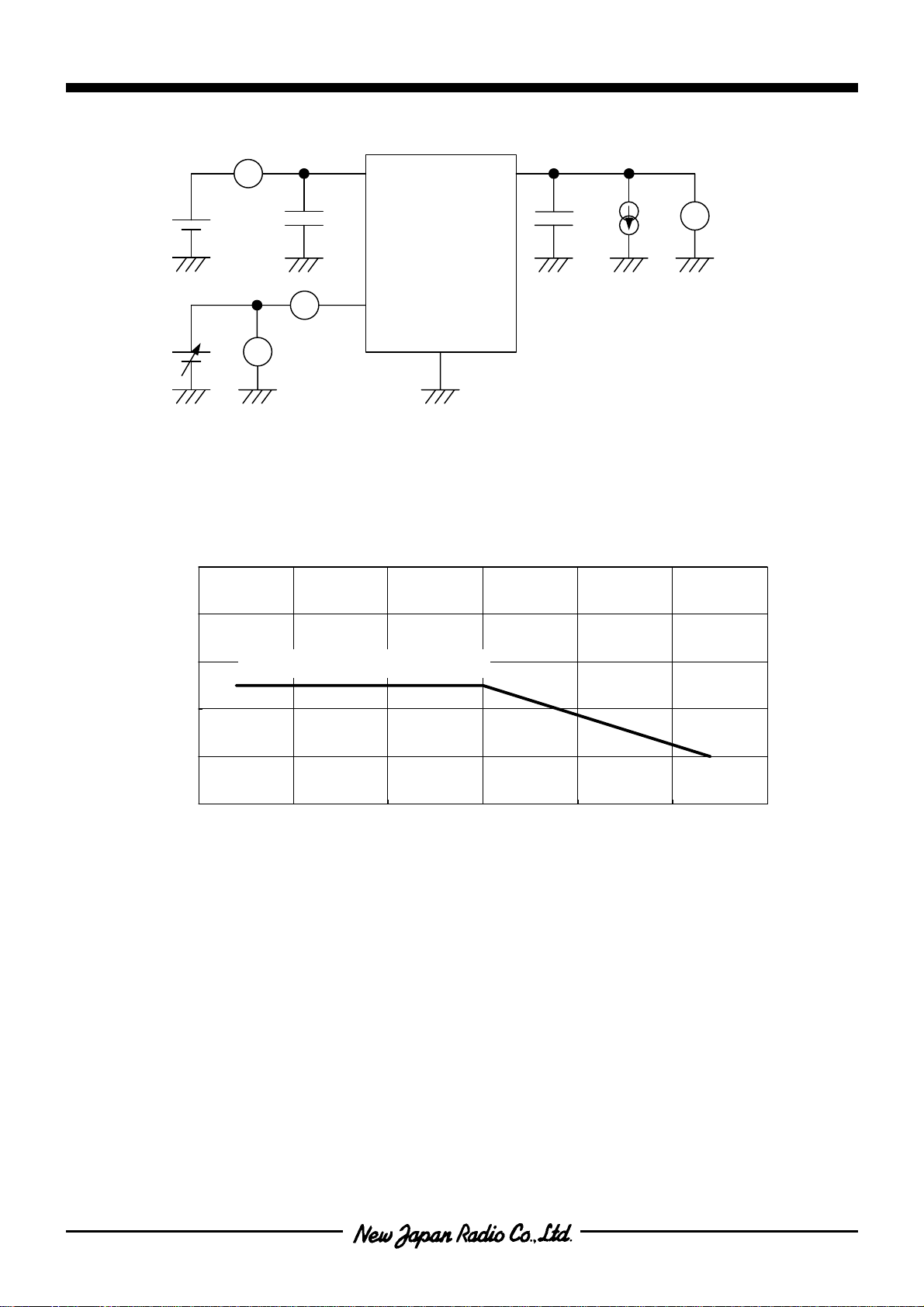
TEST CIRCUIT
P
Di
i
i
P
(
W)
NJU7777
VIN
A
IIN
0.1µF
A
I
CONT
V
IN
NJU7777
CONTROL
GND
V
V
CONT
*4 Vo≤2.0V version: Co=2.2µF(ceramic)
POWER DISSIPATION vs. AMBIENT TEMPERATURE
NJU7777F4 Power Dissipation
(Topr=-40〜+85℃,Tj=125℃)
500
V
OUT
I
*4
1.0µF
(ceramic)
V
V
OUT
OUT
Ver.2008-01-24
m
400
D
on
300
pat
ss
200
ower
100
0
-50 -25 0 25 50 75 100
On Board(114.3×76.2×1.6mm, FR-4)
Ambient Temperature Ta(℃)
-
-

NJU7777
TYPICAL APPLICATION
1 In case that ON/OFF Control is not required:
V
IN
0.1µF
V
IN
NJU7777
CONTROL
GND
V
OUT
V
OUT
1.0µF *5
*5Vo≤2.0V version: Co=2.2µF
Connect control terminal to VIN terminal.
2 In use of ON/OFF Control
V
IN
0.1µF
*5Vo≤2.0V version: Co=2.2µF
State of control terminal:
● “H” → output is enabled.
● “L” or “open” → output is disabled.
V
CONTROL
IN
NJU7777
GND
V
OUT
V
OUT
1.0µF *5
-
-
Ver.2008-01-24

TYPICAL CHARACTERISTICS
NJU7777_3.0V
3.2
3.1
3
2.9
Output Voltage : Vo(V)
2.8
Output Voltage vs. In put V o ltage
Io=0A
Io=100mA
@:Ta=25oC
Co =1.0 µF(Ceramic)
Io=30 mA
NJU7777
4
3.5
3
2.5
2
1.5
Output Voltage : Vo(V)
1
0.5
Output Vol tage vs. Output Current
NJU7777_3.0V
@:Ta=25oC
Co=1 .0µF(Ceramic)
V
IN=4V
2.7
2.7 2.8 2.9 3 3.1 3.2 3.3 3.4
100
80
60
40
Ground Pin Current : IGND (µ A)
20
0
4
Inp ut Volta ge : VIN(V)
Ground Pin Current v.s. Output Current
050100150
Output Voltage vs. C o n tr o l Vol tag e
NJU7777_3.0V
Output Current : I
NJU7777_3.0V
@:Ta=25oC
V
IN=4 .0V
Co=1.0 µF
O(mA)
(Ceramic)
0
0 50 100 150 200 250 300
0.4
@:Ta=25oC
Co =1.0 µF
0.35
0.3
0.25
0.2
0.15
Dropout Voltage:dVI-O (V)
0.1
0.05
0
050100150
Output Current : Io(mA)
Dropout Voltage vs. Output Current
NJU7777_3.0V
(Ceramic)
Output Curr ent:Io(m A)
0
Load Regulation vs. Output Current
NJU7777_3.0V
3.5
2.5
1.5
Output Voltage : Vo(V)
0.5
Ver.2008-01-24
3
2
1
@:Ta=25oC
IN=4.0V
V
Co=1.0 µF
0
0 0.5 1 1.5 2 2.5 3
(Ceramic)
Control Voltage : Vcont(V)
-5
-10
-15
-20
-25
-30
Load Regulation : dVo/dIo(mV)
@:Ta=25oC
-35
V
IN=4.0V
Co =1.0 µF
(Ceramic)
-40
050100150
Output Current : Io(mA)
-
-
NJU7777
TYPICAL CHARACTERISTICS
NJU7777_3.0V
300
250
200
Peak Output Current vs. Input Voltage
40
35
30
25
Quiescent Current v.s. Input Voltage
NJU7777_3.0V
@:Ta=25oC
Output is open.
Co=1.0 µF
(Ceramic)
including Icont
150
100
Peak Output Current : IoMAX(mA)
50
0
3456789
120
100
80
60
40
Out p u t N o i se Vol tage : Vn(u V r ms)
20
0
0.001 0.01 0.1 1 10 100
100
90
80
70
@:Ta=25oC
Co=1 .0µF(Ceramic)
Input Voltag e : V
Output Noise Voltage vs. Output Current
NJU7777_3.0V
IN(V)
@:Ta=25oC
V
IN=4 .0V
LPF:80 kHz
IN=0 .1µF(Ceramic)
C
Co=1.0µF(Ceramic)
Output Current : Io(mA)
Rip ple Rejection v s. O utput Cur rent
NJU7777_3.0V
@:Ta=25oC
V
IN=4.0V
ein=20 0mVrms
Co=1.0 µF
(C eramic )
f=1kHz
20
15
10
Quiescent Current : IQ (µA)
5
0
02468
100
80
60
40
@:Ta=25oC
20
Ripple Rejection Ratio : RR (dB)
V
IN=4.0V
ein=200µVrms
Co=1.0 µF
CIN=0 .1µF
0
10 100 1k 10k 100k
Equivalent Seris e Res is tance vs. Output Current
100
@:Ta=25oC
V
IN=4.0V
Co=1 .0µF
CIN=0.1µF(Ceramic)
10
Input Voltage : VIN(V)
Rip ple Rejection Rat io v .s. Frequ ency
NJU7777_3.0V
Io=0mA
Io=10mA
Io=30mA
(Ceramic)
Frequenc y : f (Hz)
NJU7777_3.0V
(C eramic)
60
50
40
Ripple Rejection : RR (dB)
30
20
0.001 0.01 0.1 1 10 10 0
Output Current : Io(mA)
f=10kHz
1
0.1
Equivalen t Ser i se Resi stan ce : ESR(Ω)
0.001 0.01 0.1 1 10 100
STA B LE RE G I ON
Output Current : Io(mA)
-
-
Ver.2008-01-24

TYPICAL CHARACTERISTICS
NJU7777_3.0V
0.3
0.25
0.2
Dropou t Vol tag e v.s. Temperatur e
@:Io=100mA
Co=1.0 µF
CIN=0 .1 µF
(Ceramic)
NJU7777
2
1.5
Control Voltage(OFF) v.s. Temperature
NJU7777_3.0V
@:VIN=4.0V
Co=1.0 µF(Ceramic)
C
IN=0 .1µF
0.15
0.1
Dropout Voltage:dVI-O (V)
0.05
0
3.1
3.05
3
Outp ut Volta ge Vo (V)
2.95
-50 0 50 100 150
Temperature : Ta (oC)
NJU7777_3.0V
Output Voltage v.s. Temperature
@:VIN=4 .0 V
Io=30mA
Co =1.0 µF
CIN=0 .1µF
(Ceramic)
1
0.5
Control Volt age : VCONT(OFF) (V)
0
-50 0 50 100 150
400
350
300
250
200
150
100
Peak Output Current : IoMAX(mA)
50
Temperature : Ta (oC)
Peak Output Curren t v. s. Temperatur e
NJU7777_3.0V
@:VIN=4.0V
Co=1.0 µF(Cer amic)
Cin=0.1µF
2.9
40
35
30
25
20
15
10
Quiescent Current : IQ (µA)
Ver.2008-01-24
-50 0 50 10 0 150
5
0
-50 0 50 100 150
Tempera ture Ta (oC)
Quiescent Current v.s. Temperature
NJU7777_3.0
@:VIN=4 .0V
Output is open.
Co=1.0 µF(Cera mic)
C
Temperature : Ta (oC)
IN=0.1µF
0
-50 0 50 100 150
0.1
0.05
0
-0.05
Line Regulation : dVo/dIo (%/V)
-0.1
-50 0 50 100 150
Temperature : Ta (oC)
NJU7777_3.0V
Line Regulation v.s. Temperature
@:dVIN=4.0- 8.0V
Io=30mA
Co=1.0 µF(Ceramic)
C
IN=0 .1µF
Temperature : Ta (oC)
-
-

NJU7777
TYPICAL CHARACTERISTICS
NJU7777_3.0V
0.03
0.025
0.02
Load Regula tio n v. s. Temperature
@:VIN=4 .0V
Io=0-10 0mA
Co=1. 0µF
CIN=0. 1µF
(Ceramic)
NJU7777_3.0V
Output Voltage v.s.Temperature
(Ceramic)
CIN=0. 1µF
3.5
2.5
4
3
@:VIN=4.0V
Io=30mA
Co =1.0 µF
0.015
0.01
Load Regulation : dVo/dIo (%/mA)
0.005
0
200
150
100
50
Short Circuit Current : ISC (mA)
-50 0 50 100 150
Short Circui t C urrent v.s. Temperature
Temperature : Ta (oC)
NJU7777_3.0V
@:VIN=4 .0V
Output is short to ground.
Co=1. 0µF(Cera mic)
Cin=0.1µF
2
1.5
Output Voltage Vo (V)
1
0.5
0
-50 0 50 100 15 0 200
Tempera ture Ta (oC)
0
-50 0 50 100 150
Temperature : Ta (oC)
-
-
Ver.2008-01-24
TYPICAL CHARACTERISTICS
NJU7777_3.0V
7
6
5
4
3
2
1
Output Voltage : Vo [V]
0
-1
012345
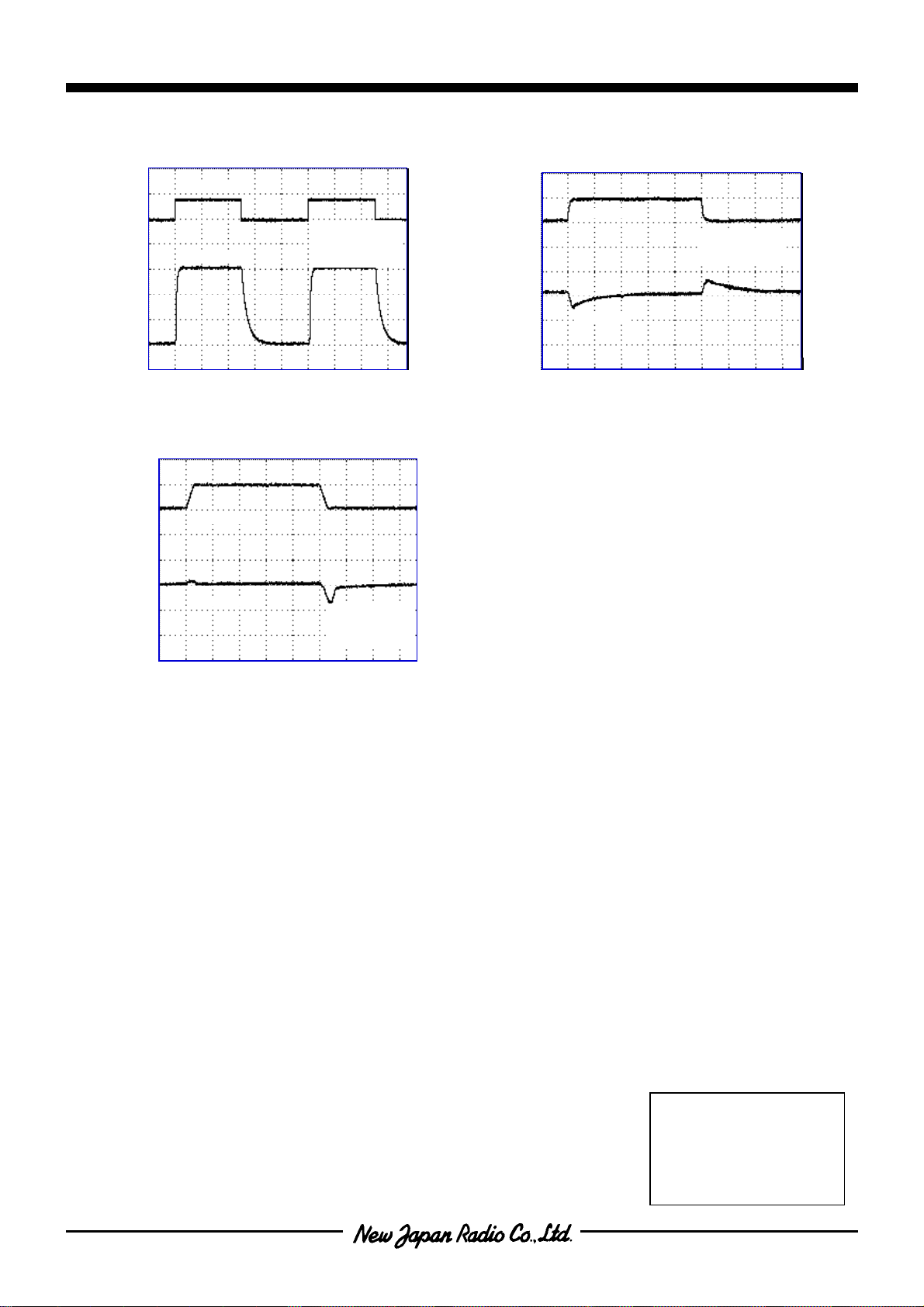
ON/OFF Transient Response
Control Voltage
Output Voltage
Time : t [mS]
NJU7777_3.0V
3.5
3.4
3.3
3.2
3.1
3
Output Voltage : Vo [V]
2.9
2.8
2.7
0 40 80 120 160 200
Line Transient Response
Input Voltage
Output Voltage
Time : t [ µS]
@:Ta=25oC
IN=4.0V
V
Co=1.0µF(Ceramic)
Io=30mA
@:Ta=25oC
V
IN=4.0V
Co=1 .0µF( Cera mic)
Io=30mA
10
5
0
-5
-10
-15
-20
-25
-30
NJU7777
NJU7777_3.0V
3.5
3.4
3.3
3.2
3.1
3
Control Voltage : Vo [V]
2.9
Output Vol tage : Vo [V]
2.8
2.7
0 40 80 120 160 200
6
5
4
[V]
IN
3
2
1
Input Voltage : V
0
-1
-2
Load Transien t Response
Output Current
Output Voltage
Time : t [ µS]
@:Ta=25oC
IN=4.0V
V
Co =1.0 µF(Cera mic)
150
100
50
0
-50
-100
-150
-200
-250
Output C ur re n t : Io [mA ]
Ver.2008-01-24
[CAUTION]
The specifications on this databook are only
given for information , without any guarantee
as regards either mistakes or omissions. The
application circuits in this databook are
described only to show representative usages
of the product and not intended f or the
guarantee or permission of any right including
the industrial rights.
-
-

 Loading...