

Low Dropout Voltage Regulator
GENERAL DESCRIPTION
■■■■
The NJU7250 series is low dropout voltage and high
precision positive voltage regulator with ON/O FF cont rol.
This IC is suitable for the battery items because of low
operating current and 150mA output cur r ent .
Furthermore, this series is packaged with MTP5
FEATURES
■■■■
• Low Operating Current
• Output Current
• High Precision Output Voltage
• Low Dropout Voltage
35µA typ.
150mA
Vo±2%
0.2V typ.
• Standby Function
• Short Current Protection Circuit
• C-MOS Technology
• Package Outline
MTP5
OUTPUT VOLTAGE LINE-UP
■■■■
Device Name V
OUT
NJU7250F25 2.5V
Device Name V
NJU7250F30 3.0V
NJU7250F27 2.7V NJU7250F32 3.2V
NJU7250F28 2.8V
NJU7250F33 3.3V
NJU7250F29 2.9V
TERMINAL DESCRIPTION
■■■■
No. Symbol Function
1 VIN Input
2 GND GND
3 STB
H: Regulation
L: Standby, Output off
4 NC Non Connection
5 V
Output
OUT
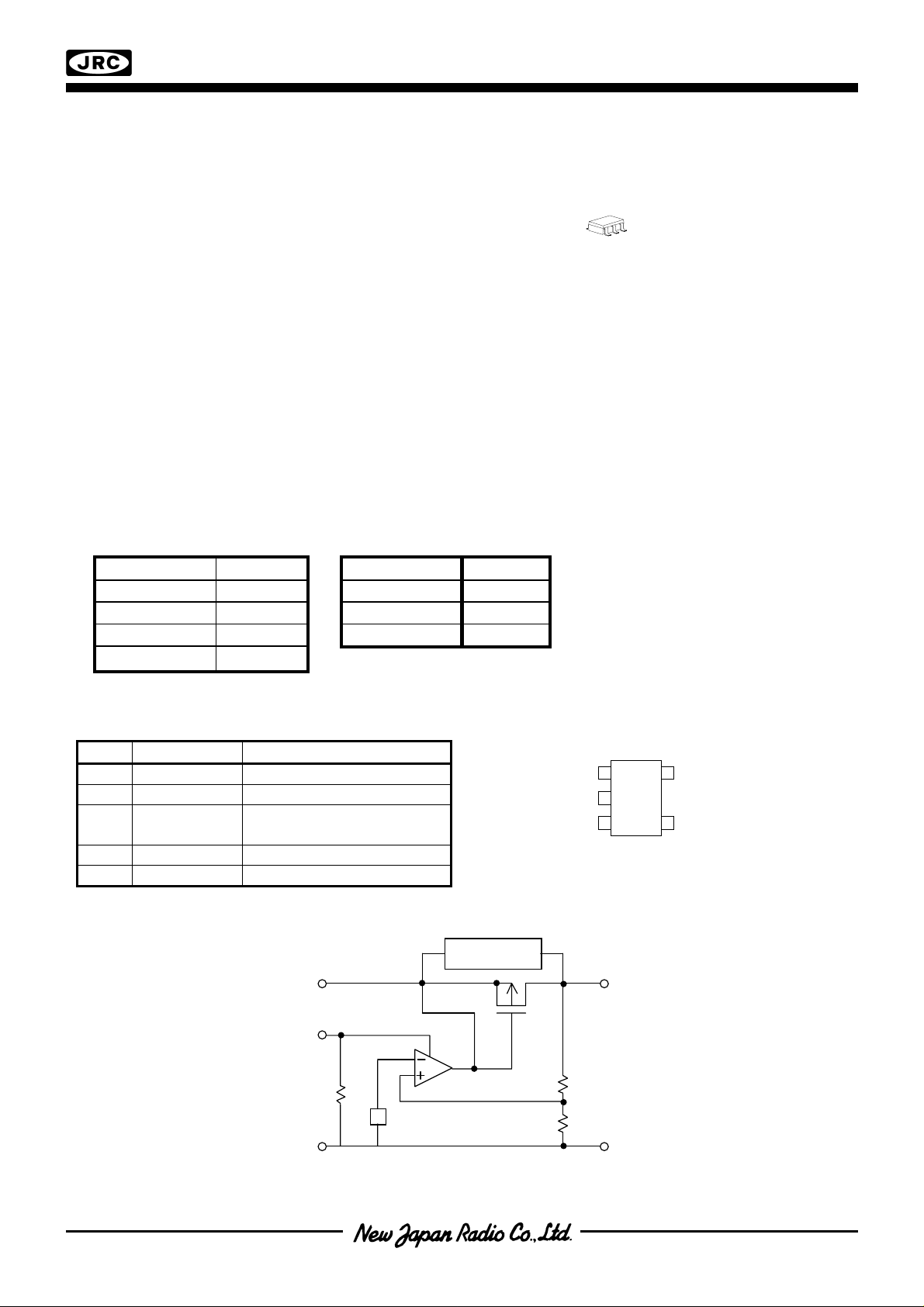
EQUIVALENT CIRCUIT
■■■■
VIN
STB
GND
Vref
@Io=100mA, 2.8V≤Vo≤3.3V
Short Current
Protection Circuit
PACKAGE OUTLINE
■■■■
NJU7250F
OUT
PIN CONFIGURATION
■■■■
1 5
2
3 4
VOUT
GND
NJU7250
- 1/3 -
ABSOLUTE MAXIMUM RATINGS
■■■■
Parameter Symbol Ratings Unit
Input Voltage V
Control Voltage V
Output Voltage V
Output Current I
IN
CONT
OUT
OUT
Power Dissipation PD 250 mW
Operating Temperature Topr
Storage Temperature Tstg
ELECTRICAL CHARACTERISTICS
■■■■
Parameter Symbol Condition MIN. TYP. MAX. Unit
Output Voltage V
O
Output Current IO
Dropout Voltage
Operating Current I
Standby Current I
Load Regulation
Line Regulation
Output Voltage
Temperature Coefficient
Input Voltage V
Short Current Limit I
Pull-down Resistance
H Level Control Voltage V
L Level Control Voltage V
V
∆
Q
Q(OFF)
/∆IO VIN=VO+1V, 1mA≤I
V
∆
O
V
∆
V
V
⋅
∆
IN
/∆T -40≤Ta≤+85°C, IO=10mA
V
∆
O
IN
LIM
RPD
CONT(ON)
CONT(OFF)
Output Noise Voltage VNO
NJU7250
(Ta=25°C)
9 V
GND-0.3 ∼ V
+0.3
IN
GND-0.3 ∼ VIN+0.3
200 mA
-40 ∼ +85
-40 ∼ +150
VIN=VO+1V, 1mA≤I
1.5≤V
1.8≤V
≤
O
≤
O
1.7, V
5.0, V
IN=VO
IN=VO
≤
O
+1V
+1V
VO=1.5V, IO=100mA 0.5
VO=1.6V, IO=100mA 0.4
VO=1.7V, IO=100mA 0.3
1.8≤V
IO
2.0≤V
2.5≤V
2.8≤V
3.4≤V
VIN=VO+1V, V
VIN=VO+1V, V
/
O
V
OUT
IN=VO
≤
O
≤
O
≤
O
≤
O
≤
O
1.9, I
2.4, I
2.7, I
3.3, I
5.0, I
=100mA
O
=100mA
O
=100mA
O
=100mA
O
=100mA
O
CONT(ON)=VIN
CONT(OFF)
≤
O
+0.5V∼8V, IO=30mA
8 V
VO=0V 50 mA
2.5 5 10
1.5 VIN V
0 0.25 V
f=10Hz∼100kHz
V
V
C
°
C
°
(C
=0.1µF, CO=2.2µF, Ta=25°C)
IN
30mA
-2% +2% V
100
150
mA
0.60 1.40
0.35 0.70
0.24 0.35
0.20 0.30
0.17 0.26
35 70
=GND 0.1 1.0
80mA
12 40 mV
0.05 0.2 %/V
100
±
ppm/°C
MΩ
30
V/rms
µ
V
A
µ
A
µ
-
-
2/3
NJU7250
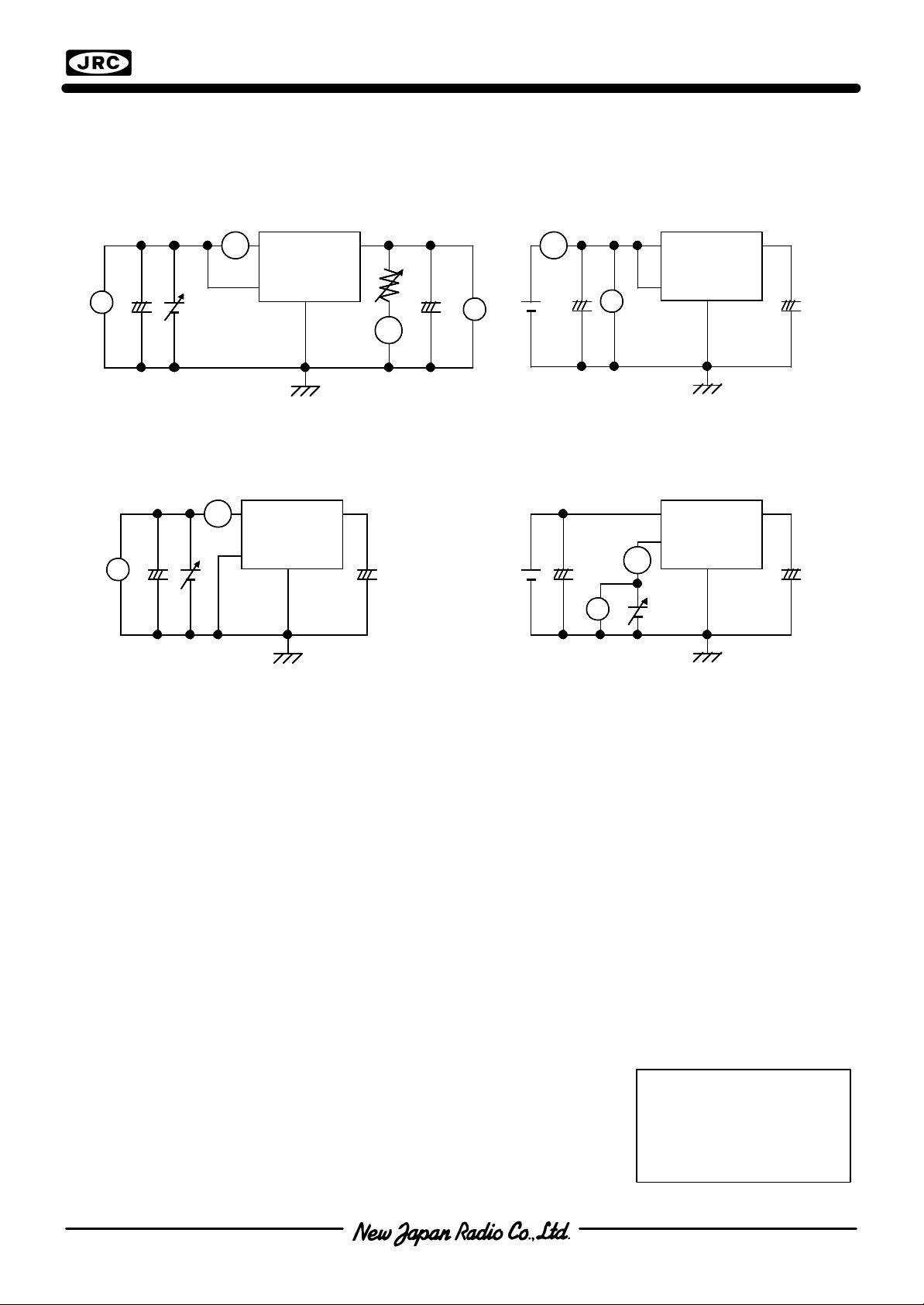
ν TEST CIRCUIT
[CAUTION]
1. Output Voltage, Output Current, Dropout Voltage, 2. Input Voltage
Operating Current, Line Regulation , Line Regulation,
Output Voltage Temperature Coefficient,
Short Current Limit
V
V
V
A
A
A
V
V
V
IN
IN
IN
STB
STB
STB
GND
GND
GND
V
V
V
OUT
OUT
OUT
A
A
A
V
V
V
A
A
A
V
V
V
V
V
V
IN
IN
IN
STB
STB
STB
GND
GND
GND
3. Standby Current 4. H Level Control Voltage,
L Level Control Voltage,
Pull-down Resistance
V
V
V
A
A
A
V
V
V
IN
IN
IN
STB
STB
STB
GND
GND
GND
V
V
V
OUT
OUT
OUT
V
V
V
A
A
A
V
V
V
IN
IN
IN
STB
STB
STB
GND
GND
GND
V
V
V
OUT
OUT
OUT
V
V
V
OUT
OUT
OUT
The specifications on this databook are only
given for information , without any guarantee
as regards either mistakes or omissions. The
application circuits in this databook are
described only to show representative usages
of the product and not intended for the
guarantee or permission of any right including
the industrial rights.
- 1/1 -

 Loading...