JRC NJU6677CL Datasheet
NJU6677NJU6677
PRELIMINARYPRELIMINARY
88-common x 132-segment88-common x 132-segment
BIT MAP LCD DRIVER BIT MAP LCD DRIVER
GENERAL DESCRIPTION GENERAL DESCRIPTION
The NJU6677 is a bit map LCD driver to display graphics or charac-The NJU6677 is a bit map LCD driver to display graphics or characters. It contains 15,840 bits display data RAM, microprocessor inter-ters. It contains 15,840 bits display data RAM, microprocessor interface circuits, instruction decoder, 132-segment and 88-common driv-face circuits, instruction decoder, 132-segment and 88-common drivers.ers.
The bit image display data is transferred to the display data RAM byThe bit image display data is transferred to the display data RAM by
serial or 8-bit parallel interface.serial or 8-bit parallel interface.
The NJU6677 displays 88 x 132 dots graphics or 8-character 5-line byThe NJU6677 displays 88 x 132 dots graphics or 8-character 5-line by
16 x 16 dots character.16 x 16 dots character.
It oscillates by built-in OSC circuit without any external components.It oscillates by built-in OSC circuit without any external components.
Furthermore, the NJU6677 features Partial Display Function whichFurthermore, the NJU6677 features Partial Display Function which
creates up to 2 blocks of active display area and optimizes duty cyclecreates up to 2 blocks of active display area and optimizes duty cycle
ratio. This function sets optimum boosted voltage by the combinationratio. This function sets optimum boosted voltage by the combination
with both of programmable 5-time voltage booster circuit and 201-with both of programmable 5-time voltage booster circuit and 201step electrical variable resistor. As result, it reduces the operating cur-step electrical variable resistor. As result, it reduces the operating current.rent.
The operating voltage from 2.4V to 3.6V and low operating current areThe operating voltage from 2.4V to 3.6V and low operating current are
useful for small size battery operating items.useful for small size battery operating items.
FEATURES FEATURES
Direct Correspondence between Display Data RAM and LCD Pixel Direct Correspondence between Display Data RAM and LCD Pixel
Display Data RAM - 15,840 bits Display Data RAM - 15,840 bits
220 LCD Drivers - 88-common and 132-segment 220 LCD Drivers - 88-common and 132-segment
Direct Microprocessor Interface for both of 68 and 80 type MPU Direct Microprocessor Interface for both of 68 and 80 type MPU
Serial Interface Serial Interface
Partial Display Function Partial Display Function
((2 blocks of active display area and automatic 2 blocks of active display area and automatic duty cycle ratio selection)duty cycle ratio selection)
Easy Vertical Scroll by the variable start line address and over size display data RAM Easy Vertical Scroll by the variable start line address and over size display data RAM
Programmable Bias selection ; 1/4,1/5,1/6,1/7,1/8,1/9,1/10 bias Programmable Bias selection ; 1/4,1/5,1/6,1/7,1/8,1/9,1/10 bias
Common Driver Order Assignment by mask option Common Driver Order Assignment by mask option
Version Version CC00 to C to C8787(Pin name)(Pin name)
NJU6677ANJU6677A ComCom00 to Com to Com8787
NJU6677BNJU6677B ComCom8787 to Com to Com00
Useful Instruction Set Useful Instruction Set
Display Data Read/Write, Display ON/OFF Cont, Inverse Display, Page Address Set, Display Data Read/Write, Display ON/OFF Cont, Inverse Display, Page Address Set,
Display Start Line Set, Partial Display, Bias Select, Column Address Set, Status Read, Display Start Line Set, Partial Display, Bias Select, Column Address Set, Status Read,
All On/Off, Voltage Booster Circuits Multiple Select(Maximum 5-time), n-Line Inverse, All On/Off, Voltage Booster Circuits Multiple Select(Maximum 5-time), n-Line Inverse,
Read Modify Write, Power Saving, ADC Select, etc. Read Modify Write, Power Saving, ADC Select, etc.
Power Supply Circuits for LCD; Programmable Voltage Booster Circuits(5-time Maximum), Power Supply Circuits for LCD; Programmable Voltage Booster Circuits(5-time Maximum),
Regulator, Voltage Follower x 4 Regulator, Voltage Follower x 4
Precision Electrical Variable Resistance Precision Electrical Variable Resistance
Low Power Consumption Low Power Consumption
Operating Voltage Operating Voltage --- 2.4V to 3.6V --- 2.4V to 3.6V
LCD Driving Voltage LCD Driving Voltage --- 6.0V to 18V --- 6.0V to 18V
Package Outline Package Outline --- COF / TCP / Bumped Chip --- COF / TCP / Bumped Chip
C-MOS Technology C-MOS Technology
PACKAGE OUTLINE PACKAGE OUTLINE
NJU6677CLNJU6677CL
JUL.10.2000JUL.10.2000
Ver.2.1 Ver.2.1
NJU6677NJU6677
PAD LOCATION PAD LOCATION
43
0
C
S
S
1
S
2
0
C
DUMMY4
DUMMY3
DUMMY2
DUMMY1
V
DD
V
1
V
2
V
3
V
4
V
5
VR
V
DD
-
C1
+
C1
-
C2
+
C2
-
X
Y
C3
C3
C4
C4
V
V
D
D
D
D
D
D
D
D
+
-
+
OUT
SS
7
6
5
4
3
2
1
0
RD
WR
A0
CS
OSC
2
OSC
1
T1
T2
VSS
RES
SEL68
P/S
VDD
1
DUMMY0
S
129
S
130
87
131
C
S
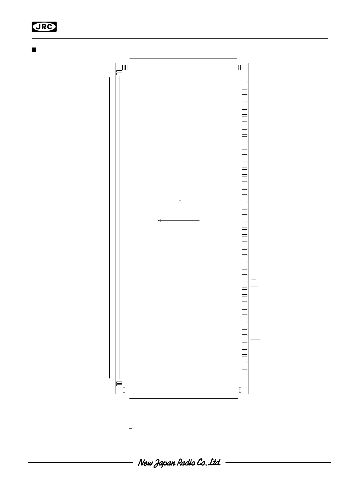
Chip CenterChip Center : X=0um,Y=0um: X=0um,Y=0um
Chip SizeChip Size : X=8.31mm,Y=2.93mm: X=8.31mm,Y=2.93mm
Chip ThicknessChip Thickness : 675um : 675um ++ 30um 30um
Bump SizeBump Size : 45um x 83um: 45um x 83um
Pad pitchPad pitch : 60um(Min): 60um(Min)
Bump HeightBump Height : 15um TYP.: 15um TYP.
Bump MaterialBump Material : Au: Au
44
C
NJU6677NJU6677
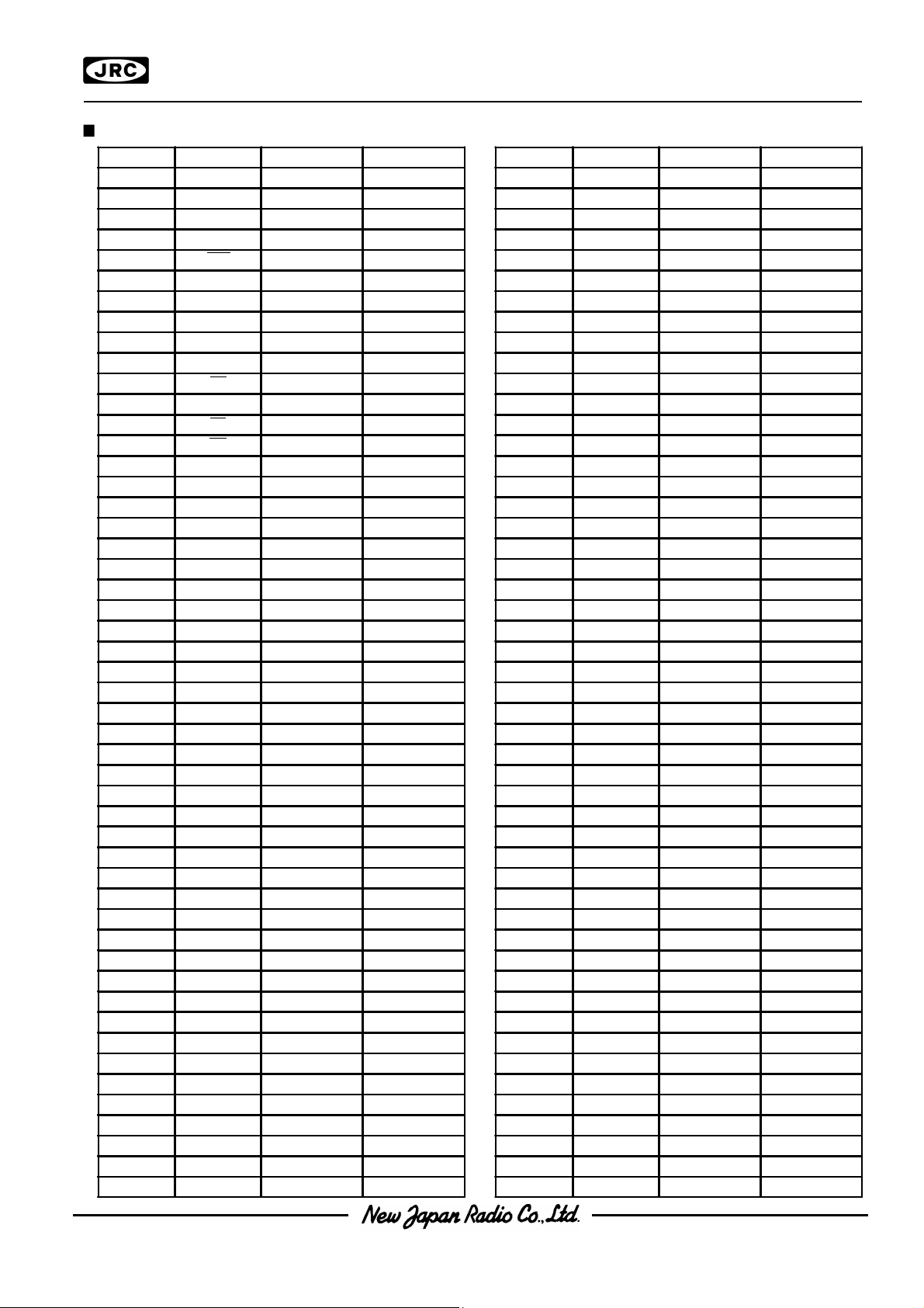
TERMINAL DESCRIPTION TERMINAL DESCRIPTION Chip Size 8.31x2.93mm (Chip Center X=0um,Y=0um)Chip Size 8.31x2.93mm (Chip Center X=0um,Y=0um)
PAD No. Terminal X= um Y= um PAD No. Terminal X= um Y= um
1 DUMMY0 -3884.0 -1305.0 51 C6 3995.0 -958.1
2 VDD -3179.2 -1305.0 52 C7 3995.0 -898.1
3 P/S -3014.1 -1305.0 53 C
8
4 SEL68 -2793.7 -1305.0 54 C9 3995.0 -778.1
5 RES -2557.3 -1305.0 55 C10 3995.0 -718.1
6 VSS -2400.1 -1305.0 56 C11 3995.0 -658.1
7 T2 -2242.9 -1305.0 57 C 12 3995.0 -598.1
8 T1 -2007.3 -1305.0 58 C 13 3995.0 -538.1
9 OSC1 -1786.9 -1305.0 59 C14 3995.0 -478.1
10 OSC2 -1550.5 -1305.0 60 C 15 3995.0 -418.1
11 CS -1330.1 -1305.0 61 C16 3995.0 -358.1
12 A0 -1093.7 -1305.0 62 C 17 3995.0 -298.1
13 WR -873.3 -1305.0 63 C18 3995.0 -238.1
14 RD -636.9 -1305.0 64 C19 3995.0 -178.1
15 D0 -400.2 -1305.0 65 C20 3995.0 -118.1
16 D1 -179.8 -1305.0 66 C21 3995.0 -58.1
17 D2 40.6 -1305.0 67 C22 3995.0 1.9
18 D
3
261.0 -1305.0 68 C
23
19 D4 481.4 -1305.0 69 C24 3995.0 121.9
20 D 5 701.8 -1305.0 70 C25 3995.0 181.9
21 D6(SCL) 922.2 -1305.0 71 C26 3995.0 241.9
22 D7(SI) 1142.6 -1305.0 72 C27 3995.0 301.9
23 VSS 1300.1 -1305.0 73 C28 3995.0 361.9
24 VOUT 1370.1 -1305.0 74 C29 3995.0 421.9
25 C4
26 C4
27 C3
28 C3
29 C2
30 C2
31 C1
32 C1
+
-
+
-
+
-
+
-
1466.0 -1305.0 75 C30 3995.0 481.9
1614.8 -1305.0 76 C31 3995.0 541.9
1674.8 -1305.0 77 C
32
1823.6 -1305.0 78 C33 3995.0 661.9
1883.6 -1305.0 79 C34 3995.0 721.9
2032.4 -1305.0 80 C35 3995.0 781.9
2092.4 -1305.0 81 C36 3995.0 841.9
2241.2 -1305.0 82 C37 3995.0 901.9
33 VDD 2311.2 -1305.0 83 C38 3995.0 961.9
34 VR 2491.2 -1305.0 84 C39 3995.0 1021.9
35 V5 2561.2 -1305.0 85 C40 3995.0 1081.9
36 V
4
2631.2 -1305.0 86 C
41
37 V3 2701.2 -1305.0 87 C42 3995.0 1201.9
38 V2 2771.2 -1305.0 88 C43 3995.0 1261.9
39 V1 2841.2 -1305.0 89 S0 3995.0 1321.9
40 VDD 2911.2 -1305.0 90 S1 3870.0 1305.0
41 DUMMY1 3119.2 -1305.0 91 S2 3810.0 1305.0
42 DUMMY2 3179.2 -1305.0 92 S3 3750.0 1305.0
43 DUMMY3 3239.2 -1305.0 93 S4 3690.0 1305.0
44 DUMMY4 3884.0 -1305.0 94 S5 3630.0 1305.0
45 C
0
3995.0 -1318.1 95 S
6
46 C1 3995.0 -1258.1 96 S7 3510.0 1305.0
47 C2 3995.0 -1198.1 97 S8 3450.0 1305.0
48 C3 3995.0 -1138.1 98 S9 3390.0 1305.0
49 C4 3995.0 -1078.1 99 S10 3330.0 1305.0
50 C 5 3995.0 -1018.1 100 S11 3270.0 1305.0
3995.0 -838.1
3995.0 61.9
3995.0 601.9
3995.0 1141.9
3570.0 1305.0
NJU6677NJU6677
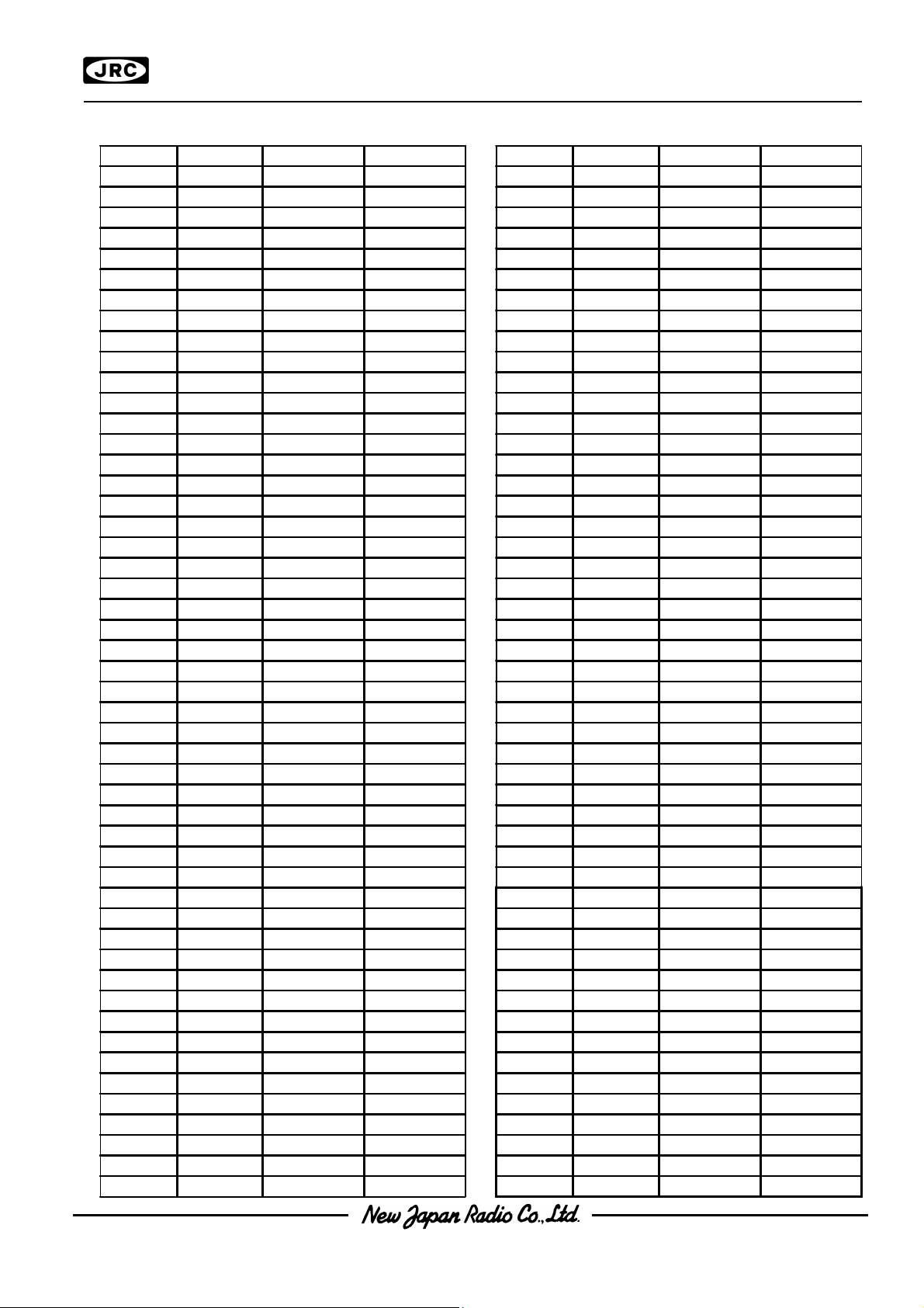
PAD No. Terminal X= um Y= um PAD No. Terminal X= um Y= um
101 S
12
3210.0 1305.0 151 S
102 S13 3150.0 1305.0 152 S63 150.0 1305.0
103 S14 3090.0 1305.0 153 S64 90.0 1305.0
104 S
15
3030.0 1305.0 154 S
105 S16 2970.0 1305.0 155 S66 -30.0 1305.0
106 S17 2910.0 1305.0 156 S67 -90.0 1305.0
107 S
18
2850.0 1305.0 157 S
108 S19 2790.0 1305.0 158 S69 -210.0 1305.0
109 S20 2730.0 1305.0 159 S70 -270.0 1305.0
110 S21 2670.0 1305.0 160 S71 -330.0 1305.0
111 S22 2610.0 1305.0 161 S72 -390.0 1305.0
112 S
23
2550.0 1305.0 162 S
113 S24 2490.0 1305.0 163 S74 -510.0 1305.0
114 S25 2430.0 1305.0 164 S75 -570.0 1305.0
115 S26 2370.0 1305.0 165 S76 -630.0 1305.0
116 S27 2310.0 1305.0 166 S77 -690.0 1305.0
117 S28 2250.0 1305.0 167 S78 -750.0 1305.0
118 S29 2190.0 1305.0 168 S79 -810.0 1305.0
119 S30 2130.0 1305.0 169 S80 -870.0 1305.0
120 S31 2070.0 1305.0 170 S81 -930.0 1305.0
121 S32 2010.0 1305.0 171 S82 -990.0 1305.0
122 S33 1950.0 1305.0 172 S83 -1050.0 1305.0
123 S
34
1890.0 1305.0 173 S
124 S35 1830.0 1305.0 174 S85 -1170.0 1305.0
125 S36 1770.0 1305.0 175 S86 -1230.0 1305.0
126 S
37
1710.0 1305.0 176 S
127 S38 1650.0 1305.0 177 S88 -1350.0 1305.0
128 S39 1590.0 1305.0 178 S89 -1410.0 1305.0
129 S
40
1530.0 1305.0 179 S
130 S41 1470.0 1305.0 180 S91 -1530.0 1305.0
131 S
132 S
42
43
1410.0 1305.0 181 S
1350.0 1305.0 182 S
133 S44 1290.0 1305.0 183 S94 -1710.0 1305.0
134 S
45
1230.0 1305.0 184 S
135 S46 1170.0 1305.0 185 S96 -1830.0 1305.0
136 S47 1110.0 1305.0 186 S97 -1890.0 1305.0
137 S48 1050.0 1305.0 187 S98 -1950.0 1305.0
138 S49 990.0 1305.0 188 S99 -2010.0 1305.0
139 S50 930.0 1305.0 189 S100 -2070.0 1305.0
140 S51 870.0 1305.0 190 S101 -2130.0 1305.0
141 S52 810.0 1305.0 191 S102 -2190.0 1305.0
142 S53 750.0 1305.0 192 S103 -2250.0 1305.0
143 S54 690.0 1305.0 193 S104 -2310.0 1305.0
144 S55 630.0 1305.0 194 S105 -2370.0 1305.0
145 S56 570.0 1305.0 195 S106 -2430.0 1305.0
146 S57 510.0 1305.0 196 S107 -2490.0 1305.0
147 S58 450.0 1305.0 197 S108 -2550.0 1305.0
148 S
59
390.0 1305.0 198 S
149 S60 330.0 1305.0 199 S110 -2670.0 1305.0
150 S61 270.0 1305.0 200 S111 -2730.0 1305.0
62
65
68
73
84
87
90
92
93
95
109
210.0 1305.0
30.0 1305.0
-150.0 1305.0
-450.0 1305.0
-1110.0 1305.0
-1290.0 1305.0
-1470.0 1305.0
-1590.0 1305.0
-1650.0 1305.0
-1770.0 1305.0
-2610.0 1305.0
NJU6677NJU6677
PAD No. Terminal X= um Y= um PAD No. Terminal X= um Y= um
201 S112 -2790.0 1305.0 251 C 57 -3995.0 -538.1
202 S113 -2850.0 1305.0 252 C 56 -3995.0 -598.1
203 S114 -2910.0 1305.0 253 C 55 -3995.0 -658.1
204 S115 -2970.0 1305.0 254 C 54 -3995.0 -718.1
205 S116 -3030.0 1305.0 255 C 53 -3995.0 -778.1
206 S117 -3090.0 1305.0 256 C 52 -3995.0 -838.1
207 S118 -3150.0 1305.0 257 C51 -3995.0 -898.1
208 S119 -3210.0 1305.0 258 C 50 -3995.0 -958.1
209 S120 -3270.0 1305.0 259 C 49 -3995.0 -1018.1
210 S 121 -3330.0 1305.0 260 C 48 -3995.0 -1078.1
211 S122 -3390.0 1305.0 261 C47 -3995.0 -1138.1
212 S123 -3450.0 1305.0 262 C 46 -3995.0 -1198.1
213 S124 -3510.0 1305.0 263 C 45 -3995.0 -1258.1
214 S125 -3570.0 1305.0 264 C44 -3995.0 -1318.1
215 S126 -3630.0 1305.0
216 S127 -3690.0 1305.0
217 S128 -3750.0 1305.0
218 S129 -3810.0 1305.0
219 S130 -3870.0 1305.0
220 S 131 -3995.0 1321.9
221 C87 -3995.0 1261.9
222 C86 -3995.0 1201.9
223 C85 -3995.0 1141.9
224 C
225 C83 -3995.0 1021.9
226 C82 -3995.0 961.9
227 C 81 -3995.0 901.9
228 C80 -3995.0 841.9
229 C79 -3995.0 781.9
230 C78 -3995.0 721.9
231 C77 -3995.0 661.9
232 C76 -3995.0 601.9
233 C75 -3995.0 541.9
234 C
235 C73 -3995.0 421.9
236 C72 -3995.0 361.9
237 C 71 -3995.0 301.9
238 C
239 C69 -3995.0 181.9
240 C68 -3995.0 121.9
241 C67 -3995.0 61.9
242 C66 -3995.0 1.9
243 C65 -3995.0 -58.1
244 C
245 C63 -3995.0 -178.1
246 C62 -3995.0 -238.1
247 C 61 -3995.0 -298.1
248 C60 -3995.0 -358.1
249 C59 -3995.0 -418.1
250 C58 -3995.0 -478.1
84
74
70
64
-3995.0 1081.9
-3995.0 481.9
-3995.0 241.9
-3995.0 -118.1
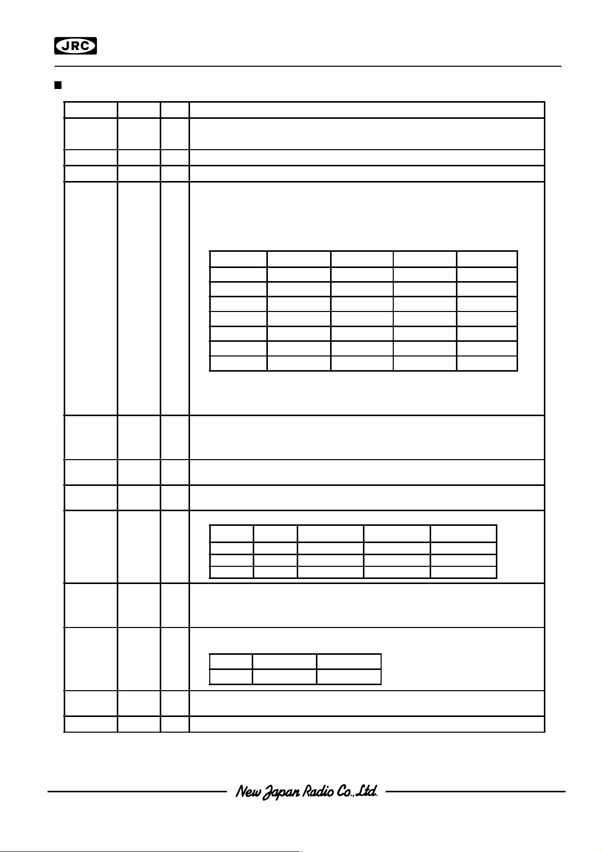
BLOCK DIAGRAM BLOCK DIAGRAM
NJU6677NJU6677
V
V
V1to V
T1,T
SS
DD
5
C1+
C1-
C2+
C2-
C3+
C3-
C4+
C4-
VR
5
Voltage
Generator
C
D r i v e r
R e g i s t e r
0
C O M
S h i f t
C
43
S
S
0
S E G
D r i v e r
C
131
87
C O M
D r i v e r
S h i f t
R e g i s t e r
C
44
COMSEG
Timing
Generator
D i s p l a y D a t a L a t c h
2
Register
Display Data RAM
120 x 132
Output Assignment
Row Address Decoder
Line Address Decoder
Start Line Register
L i n e C o u n t e r
R e gis t e r
I / O B u f f e r
P a g e A d d re ss
Instruct ionDecoder
I n t e r n a l B u s
R e s e t
RES
Culumn Address Decoder
Culumn Address Counter
Culumn Address Register
M u l t i p l e x e r
S t a t u s
M P U I n t e r f a c e
CS
A0
B F
RD
B u s H o l d e r
SEL68
WR
P/S
Display
Timing
Generator
OSC.
D0to D7(SI,S CL)
OSC1
OSC2
TERMINAL DESCRIPTION TERMINAL DESCRIPTION
No. Symbol I/O F u n c t i o n
1,41 to 44
2,33,40 VDD
DUMMY0
to
DUMMY4
Dummy Terminals.
These terminals are insulated.
Power
VDD=+3V
6,23 VSS GND VSS=0V
39,
38,
37,
36,
35
V1
V2
V3
V4
V5
Power
LCD Driving Voltage Supplying Terminal. When the internal voltage booster is
not used, supply each level of LCD driving voltage from outside with following
relation.
VDD>V1>V2>V3>V4>V5
When the internal power supply is on, the internal circuits generate and supply
== ==
==
==
==
following LCD bias voltage from V1 to V 4 terminals.
Bias V1 V2 V3 V4
1/4Bias V5+3/4VLCD V5+2/4VLCD V5+2/4VLCD V5+1/4VLCD
1/5Bias V5+4/5VLCD V5+3/5VLCD V5+2/5VLCD V5+1/5VLCD
1/6Bias V5+5/6VLCD V5+4/6VLCD V5+2/6VLCD V5+1/6VLCD
1/7Bias V5+6/7VLCD V5+5/7VLCD V5+2/7VLCD V5+1/7VLCD
1/8Bias V5+7/8VLCD V5+6/8VLCD V5+2/8VLCD V5+1/8VLCD
1/9Bias V5+8/9VLCD V5+7/9VLCD V5+2/9VLCD V5+1/9VLCD
1/10Bias V5+9/10VLCD V5+8/10VLCD V5+2/10VLCD V5+1/10VLCD
NJU6677NJU6677
(VLCD =V DD-V5)
31,32,
29,30,
27,28,
25,26
C1+,C1
C2+,C2
C3+,C3
C4+,C4
-
O Step up capacitor connecting terminals.
-
-
-
Voltage booster circuit (Maximum 5-time)
24 VOUT O Step up voltage output terminal. Connect the step up capacitor between this
terminal and VSS.
34 VR I Voltage adjust terminal. V5 level is adjusted by external bleeder resistance
connecting between VDD and V5 terminal.
8,
7
15 to 22 D0 to
T1
T2
D7
(SI)
(SCL)
I LCD bias voltage control terminals. ( *:Don't Care)
T 1 T 2
L * Available Available Available
H L Not Avail. Available Available
H H Not Avail. Not Avail. Available
Voltage
booster Cir.
Voltage Adj. V/F Cir.
I/O P/S="H" : Tri-state bi-directional Data I/O terminal in 8-bit parallel operation.
P/S="L" : D7=Serial data input terminal. D 6=Serial data clock signal input
terminal. Data from SI is loaded at the rising edge of SCL and
latched as the parallel data at 8th rising edge of SCL.
12 A0 I Connect to the Address bus of MPU. The data on the D 0 to D7 is
distinguished between Display data and Instruction by status of A0.
A0 H L
Distin. Display Data Instruction
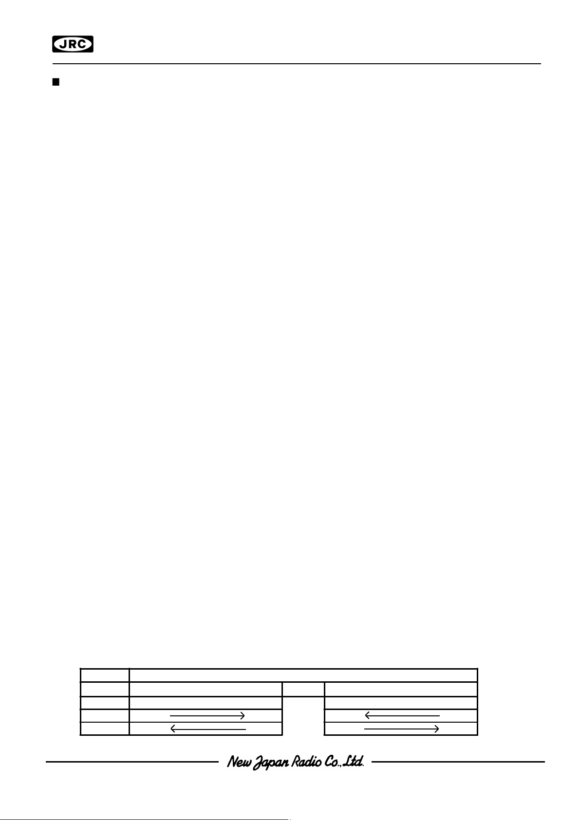
5 RES I Reset terminal. When the RES terminal goes to "L", the initialization is
performed. Reset operation is executing during "L" state of RES.
11 CS I Chip select terminal. Data Input/Output are available during CS ="L".
No Symbol I/O F u n c t i o n
14 RD(E) I <In case of 80 Type MPU>
13
WR(RW)
4 SEL68 I MPU interface type selection terminal.
3 P/S I serial or parallel interface selection terminal.
RD signal of 80 type MPU input terminal. Active "L"
During this signal is "L" , D0 to D 7 terminals are output.
<In case of 68 Type MPU>
Enable signal of 68 type MPU input terminal. Active "H"
I <In case of 80 Type MPU>
Connect to the 80 type MPU WR signal. Actie "L".
The data on the data bus input syncronizing the rise edge of this signal.
<In case of 68 Type MPU>
The read/write control signal of 68 type MPU input terminal.
R/W H L
State Read Write
SEL68 H L
State 68 Type 80 Type
P/S
"H" CS A D
"L" CS A0 SI(D7) Write Only SCL(D6)
Chip Select Data/Command
Data
0 to D7
NJU6677NJU6677
Read/Write serial Clock
RD,WR -
9,
10
OSC1
OSC2
45 to 88 C0 to
C43
89 to 220 S0 to
S131
264 to
221
C
44 to
C
RAM data and status read operation do not work in mode of
the serial interface.
In case of the serial interface (P/S="L"),RD and WR must be fixed
"H" or "L", and D0 to D 5 are high impedance.
I System clock input terminal for Maker testing.(This terminal should be Open)
For external clock operation, the clock shoud be input to OSC1 terminal.
O LCD driving signal output terminals.
Segmet output terminals:S 0 to S131
Common output terminals:C 0 to C 87
Segment output terminal
The following output voltages are selected by the combination of FR and data
in the RAM.(non of the n-line inverse functions)
RAM
O
Data
H
L
FR
H VDD V2
L V5 V3
H V2 VDD
L V
Common output terminal
The following output voltages are selected by the combination of FR and status
of common.
O
87
Scan data FR Output Voltage
H
L
H V
L V
H V
L V4
Output Voltage
Normal Reverse
3
5
DD
1
5
V
NJU6677NJU6677
Functional Description Functional Description
(1) Description for each blocks(1) Description for each blocks
(1-1) Busy Flag (BF)(1-1) Busy Flag (BF)
While the internal circuits are operating, the busy flag (BF) is "1" and any instruction excepting for the statusWhile the internal circuits are operating, the busy flag (BF) is "1" and any instruction excepting for the status
read are inhibited .read are inhibited .
The busy flag goes to “1” from DThe busy flag goes to “1” from D77 terminal when status read instruction is executed. terminal when status read instruction is executed.
When enough cycle time over than tWhen enough cycle time over than tCYCCYC indicated in “ BUS TIMING CHARACTERISTICS” is ensured, no indicated in “ BUS TIMING CHARACTERISTICS” is ensured, no
need to check the busy flag for reduction of the MPU loads.need to check the busy flag for reduction of the MPU loads.
(1-2)Display Start Line Register(1-2)Display Start Line Register
The Display start Line Register is a pointer register which indicates the address in the Display Data RAM The Display start Line Register is a pointer register which indicates the address in the Display Data RAM
corresponding with COM corresponding with COM00(normally it display the top line in the LCD Panel). This register also operates for(normally it display the top line in the LCD Panel). This register also operates for
vertical display scroll, the display page change and so on. The Display Start Line Set instruction sets the vertical display scroll, the display page change and so on. The Display Start Line Set instruction sets the
display start address of the Display Data RAM represented in 8-bit to this register. display start address of the Display Data RAM represented in 8-bit to this register.
(1-3) Line Counter(1-3) Line Counter
The Line Counter generates the line address of display data RAM by the count up operation synchronizing theThe Line Counter generates the line address of display data RAM by the count up operation synchronizing the
common cycle after the reset operation at the status change of internal FR signal.common cycle after the reset operation at the status change of internal FR signal.
(1-4) Column Address Counter(1-4) Column Address Counter
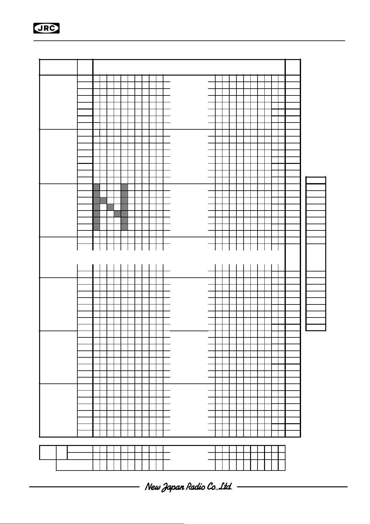
The column address counter is 8-bit pre-settable counter addressing the column address of display data RAMThe column address counter is 8-bit pre-settable counter addressing the column address of display data RAM
as shown in Fig. 1. It is incremented (+1) up to (84)as shown in Fig. 1. It is incremented (+1) up to (84)HH by the Display Data Read/Write instruction execution. by the Display Data Read/Write instruction execution.
It stops the count up operation at (84)It stops the count up operation at (84)HH, and it does not count up non existing address area over than (84), and it does not count up non existing address area over than (84)HH by by
the count lock function. This count lock is released by new column address set.the count lock function. This count lock is released by new column address set.
The column address counter is independent of the Page Register.The column address counter is independent of the Page Register.
By the Address Inverse Instruction, the column address decoder inverse the column address of Display DataBy the Address Inverse Instruction, the column address decoder inverse the column address of Display Data
RAM corresponding to the Segment Driver.RAM corresponding to the Segment Driver.
(1-5) Page Register(1-5) Page Register
The page register gives a page address of Display Data RAM as shown in Fig. 1. When the MPU accessesThe page register gives a page address of Display Data RAM as shown in Fig. 1. When the MPU accesses
the data with the page change, the page address set instruction is required.the data with the page change, the page address set instruction is required.
(1-6) Display Data RAM(1-6) Display Data RAM
Display Data RAM is the bit map RAM consisting of 15,840 bits to memorize the display data corresponding toDisplay Data RAM is the bit map RAM consisting of 15,840 bits to memorize the display data corresponding to
each pixel of LCD panel. The each bit in the Display Data RAM corresponds to the each pixel of the LCDeach pixel of LCD panel. The each bit in the Display Data RAM corresponds to the each pixel of the LCD
panel and controls the display by following bit data.panel and controls the display by following bit data.
When Normal Display : On="1" , Off="0"When Normal Display : On="1" , Off="0"
When Inverse Display : On="0" , Off="1"When Inverse Display : On="0" , Off="1"
The Display Data RAM outputs 132-bit parallel data in the area addressed by the line counter, and these dataThe Display Data RAM outputs 132-bit parallel data in the area addressed by the line counter, and these data
are set into the Display Data Latch.are set into the Display Data Latch.
The access operation from MPU to the display data RAM and the data output from the display data RAM areThe access operation from MPU to the display data RAM and the data output from the display data RAM are
so controlled to operate independently that the data rewriting does not influence with any malfunctions to theso controlled to operate independently that the data rewriting does not influence with any malfunctions to the
display.The relation between column address and segment output can inverse by the Address Inverse Instruc-display.The relation between column address and segment output can inverse by the Address Inverse Instruction ADC as shown in Fig.1.tion ADC as shown in Fig.1.
(1-7) Common Driver Assignment(1-7) Common Driver Assignment
The scanning order can be assigned by mask option as shown on Table 1.The scanning order can be assigned by mask option as shown on Table 1.
Table 1Table 1
COM Outputs Terminals
PAD No.
Pin name
Ver.A COM0 COM43 COM87 COM44
Ver.B COM87 COM44 COM0 COM43
45 88 221 264
C 0 C 43 C 87 C 44
Page Address DATA Display Pattern
D0
D1 01
D2 02
D3,D2,D1,D0
(0,0,0,0)
D3 03
D4 04
D5 05
D6 06
D7 07
D0
D1 09
D2 0A
D3,D2,D1,D0
(0,0,0,1)
D3 0B
D4 0C
D5 0D
D6 0E
D7 0F Cn Out
D0
D1 11 C1
D2 12 C2
D3,D2,D1,D0
(0,0,1,0)
D3 13 C3
D4 14 C4
D5 15 C5
D6 16 C6
D7 17 C7
D0
D1 19 C9
:
:
:
:
:
:
:
:
D6 5E C78
D7 5F C79
D0
D1 61 C81
D2 62 C82
D3,D2,D1,D0
(1,1,0,0)
D3 63 C83
D4 64 C84
Pege 12
D5 65 C85
D6 66 C86
D7 67 C87
D0
D1 69
D2 6A
D3,D2,D1,D0
(1,1,0,1)
D3 6B
D4 6C
Pege 13
D5 6D
D6 6E
D7 6F
D0
D1 71
D2 72
D3,D2,D1,D0
(1,1,1,0)
D3 73
D4 74
Pege 14
D5 75
D6 76
D7 77
| | | | | | | | | | | | | | | | | | | |
Column
Addre-
ss
D0="0"
A
D
C
D0="1"
Segment
Output
00 01 02 03 04 05 06 07 08 09
83 82 81 80 7F 7E 7D 7C 7B 7A
0 1 2 3 4 5 6 7 8 9
Fig.1 Correspondence with Display Data RAM AddressFig.1 Correspondence with Display Data RAM Address
Pege 0
Pege 1
Pege 2
:
:
:
:
7C 7D
7A 7B
09 08 07 06 05 04 03 02 01 00
122 123 124 125 126 127 128 129 130 131
7E 7F 80 81 82 83
NJU6677NJU6677
For example the
Line
Address
Display start line
is 10H
00
08
10 C0
18 C8
:
:
:
:
:
:
:
:
60 C80
68
70
NJU6677NJU6677
(1-8) Reset Circuit(1-8) Reset Circuit
Reset circuit operates the following initializations when the condition of RES terminal goes to "L" level.Reset circuit operates the following initializations when the condition of RES terminal goes to "L" level.
Initialization Initialization
11 Display OffDisplay Off
22 Normal Display (Non-inverse display)Normal Display (Non-inverse display)
33 ADC Select : Normal (ADC Instruction DADC Select : Normal (ADC Instruction D00 =”0”) =”0”)
44 Read Modify Write Mode OffRead Modify Write Mode Off
55 Internal Power supply (Voltage Booster) circuits OffInternal Power supply (Voltage Booster) circuits Off
66 Static Drive OffStatic Drive Off
77 Driver Output OffDriver Output Off
88 Clear the serial interface registerClear the serial interface register
99 Set the address(00)Set the address(00)HH to the Column Address Counter to the Column Address Counter
10 10 Set the 1st Line in the Display Start Line Register.page (00)Set the 1st Line in the Display Start Line Register.page (00)H H to the Page Address Registerto the Page Address Register
11 11 Set the page “0” to the Page Address RegisterSet the page “0” to the Page Address Register
12 12 Set the EVR register to (FF)Set the EVR register to (FF)HH
13 13 Set the All display(1/88 duty)Set the All display(1/88 duty)
14 14 Set the Bias select(1/10 Bias)Set the Bias select(1/10 Bias)
15 15 Set the 5-Time Voltage BoosterSet the 5-Time Voltage Booster
16 16 Set the n line turn over register (0)Set the n line turn over register (0)HH
The RES terminal should be connected to the Reset terminal of MPU for the initialization at the mean timeThe RES terminal should be connected to the Reset terminal of MPU for the initialization at the mean time
with MPU as shown in "MPU Interface Example". The period of reset signal requires over than 10us RES="L"with MPU as shown in "MPU Interface Example". The period of reset signal requires over than 10us RES="L"
level input as shown in "Electrical Characteristics". After 1us from the rise edge of RES signal, the operationlevel input as shown in "Electrical Characteristics". After 1us from the rise edge of RES signal, the operation
goes to normal.goes to normal.
When the internal LCD power supply is not used, the external LCD power supply into the NJU6677 must beWhen the internal LCD power supply is not used, the external LCD power supply into the NJU6677 must be
turned on during RES = "L". Although the condition of RES="L" clear each registers and initialize as above, theturned on during RES = "L". Although the condition of RES="L" clear each registers and initialize as above, the
oscillation circuit and the output terminal conditions (Doscillation circuit and the output terminal conditions (D00 to D to D77) are not influenced. The initialization must be) are not influenced. The initialization must be
performed using RES terminal at the power on, to prevent hung up or any incorrect operations. The resetperformed using RES terminal at the power on, to prevent hung up or any incorrect operations. The reset
Instruction performs the initialization procedures from No.9 to No.16 as shown in above.Instruction performs the initialization procedures from No.9 to No.16 as shown in above.
Note) The noise into the RES terminal should be eliminated to avoid the error on the application with theNote) The noise into the RES terminal should be eliminated to avoid the error on the application with the
careful design.careful design.
(1-9) LCD Driving(1-9) LCD Driving
(a) LCD Driving Circuits(a) LCD Driving Circuits
LCD driving circuits are consisted of 220 multiplexers which operate as 132 Segment drivers and 88 CommonLCD driving circuits are consisted of 220 multiplexers which operate as 132 Segment drivers and 88 Common
drivers. 88 Common drivers with the shift register scan the common display signal. The combination of thedrivers. 88 Common drivers with the shift register scan the common display signal. The combination of the
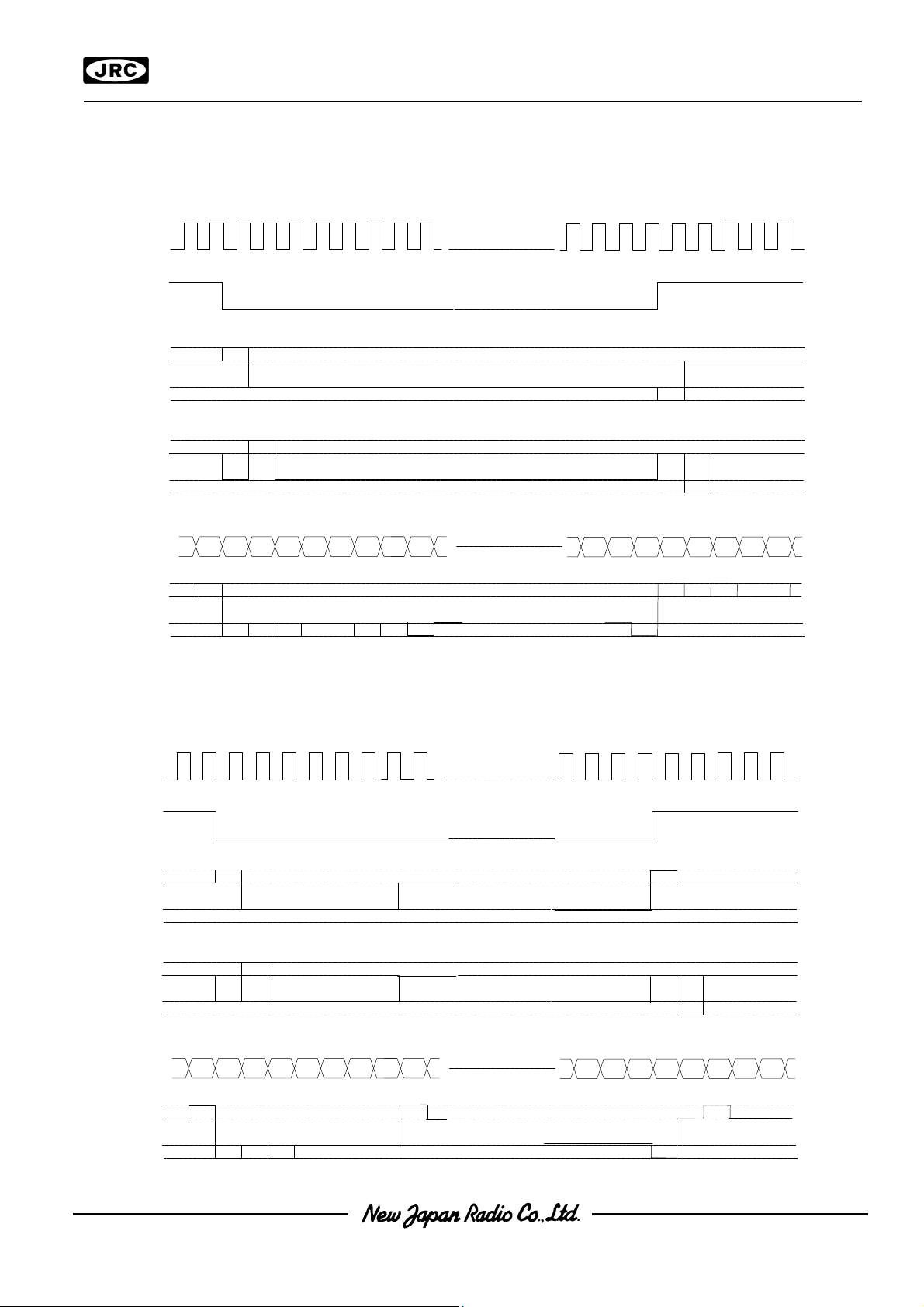
Display data, COM scan signal and FR signal form into the LCD driving output voltage. The output wave formDisplay data, COM scan signal and FR signal form into the LCD driving output voltage. The output wave form
is shown in the Fig. 7.is shown in the Fig. 7.
(b) Display Data Latch Circuits(b) Display Data Latch Circuits
Display Data Latch stores 132-bit display data temporarily which is output to LCD driver circuits at a commonDisplay Data Latch stores 132-bit display data temporarily which is output to LCD driver circuits at a common
cycle from Display Data RAM addressed by Line Counter. The instructions of Display On/Off, Display inversecycle from Display Data RAM addressed by Line Counter. The instructions of Display On/Off, Display inverse
ON/OFF and Static Drive On/Off control only the data in Display Data Latch, therefore, the data in the DisplayON/OFF and Static Drive On/Off control only the data in Display Data Latch, therefore, the data in the Display
Data RAM is not changed.Data RAM is not changed.
(c) Line Counter and Latch signal of Latch Circuits(c) Line Counter and Latch signal of Latch Circuits
The clock to Line Counter and latch signal to the Latch Circuits are generated from the internal display clockThe clock to Line Counter and latch signal to the Latch Circuits are generated from the internal display clock
(CL). The line address of Display Data RAM is renewed synchronizing with display clock(CL). 132 bits display(CL). The line address of Display Data RAM is renewed synchronizing with display clock(CL). 132 bits display
data are latched in display latch circuits synchronizing with display clock, and then output to the LCD drivingdata are latched in display latch circuits synchronizing with display clock, and then output to the LCD driving
circuits. The display data transfer to the LCD driving circuits is executed independently with RAM access bycircuits. The display data transfer to the LCD driving circuits is executed independently with RAM access by
the MPU.the MPU.
(d) Display Timing Generator(d) Display Timing Generator
Display Timing Generator generates the timing signal for the display system by combination of the masterDisplay Timing Generator generates the timing signal for the display system by combination of the master
clock CL and Driving Signal FR ( refer to Fig.2 ). The Frame Signal FR and LCD alternative signal generateclock CL and Driving Signal FR ( refer to Fig.2 ). The Frame Signal FR and LCD alternative signal generate
LCD driving waveform of the two frame alternative driving method or n-Line inverse driving method.LCD driving waveform of the two frame alternative driving method or n-Line inverse driving method.
R
NJU6677NJU6677
(e)Common Timing Generation(e)Common Timing Generation
The common timing is generated by display clock. The common timing is generated by display clock.
-Waveform of Display Timing(without the n-line inverse function, the line inverse register in set to 0) -Waveform of Display Timing(without the n-line inverse function, the line inverse register in set to 0)
87 88 1 2 3 4 5 6 7 8
C L
FR
C 0
C1
85 86 87 88 1 2 3 4 5
V
DD
V
1
V
4
V
5
V
DD
V
1
V
4
V
5
AM DATA
Sn
Fig.2 Fig.2
-Waveform of Display Timing(with the n-line inverse function, n=7, the line inverse register in set to 6) -Waveform of Display Timing(with the n-line inverse function, n=7, the line inverse register in set to 6)
87 88 1 2 3 4 5 6 7 8
CL
FR
C 0
C1
85 86 87 88 1 2 3 4 5
V
DD
V
2
V
3
V
5
V
DD
V
1
V
4
V
5
V
DD
V
1
V
4
V
5
R AMDATA
V
DD
V
Sn
2
V
3
V
5
Fig.3 Fig.3
NJU6677NJU6677
(f) Oscillation Circuit(f) Oscillation Circuit
The Oscillation Circuit is a low power CR oscillator incorporating with Resistor and Capacitor. It generatesThe Oscillation Circuit is a low power CR oscillator incorporating with Resistor and Capacitor. It generates
clocks for display timing signal source and voltage booster circuits. The oscillation circuit output frequency isclocks for display timing signal source and voltage booster circuits. The oscillation circuit output frequency is
divided as shown in below for display clock CL.divided as shown in below for display clock CL.
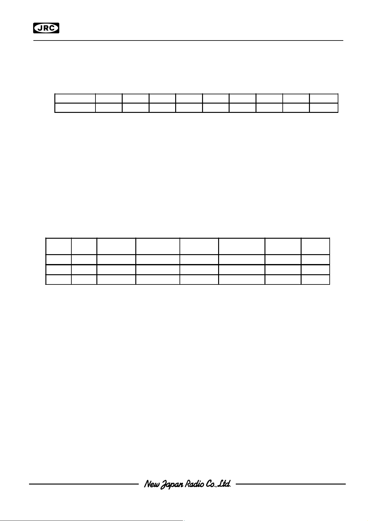
-The relation between duty and divide -The relation between duty and divide
Duty 1/8 1/16 1/24 1/32 1/40 1/48 1/56,64 1/72 1/80,88
Divide 1/44 1/22 1/15 1/11 1/9 1/7 1/6 1/5 1/4
(g) Power Supply Circuit(g) Power Supply Circuit
Internal Power Supply Circuit generate the High voltage and Bias voltage for the LCD. The power SupplyInternal Power Supply Circuit generate the High voltage and Bias voltage for the LCD. The power Supply
Circuit consists of Voltage Booster (5-Time maximum) Circuits, Regulator Circuits, and Voltage Followers.Circuit consists of Voltage Booster (5-Time maximum) Circuits, Regulator Circuits, and Voltage Followers.
The internal Power Supply is designed for small size LCD panel, therefore it is not suitable for the large sizeThe internal Power Supply is designed for small size LCD panel, therefore it is not suitable for the large size
LCD panel application. If the contrast is not good in the large size LCD panel application, please supply theLCD panel application. If the contrast is not good in the large size LCD panel application, please supply the
external.external.
The suitable values of the capacitors connecting to the VThe suitable values of the capacitors connecting to the V11 to V to V55 terminals and the voltage booster circuit, and terminals and the voltage booster circuit, and
the feedback resistors for Vthe feedback resistors for V55 operational amplifier depend on the LCD panel. And the power consumption with operational amplifier depend on the LCD panel. And the power consumption with
the LCD panel is depending on the display pattern. Please evaluate with actual LCD module.the LCD panel is depending on the display pattern. Please evaluate with actual LCD module.
The operation of internal Power Supply Circuits is controlled by the Internal Power Supply On/Off Instruction.The operation of internal Power Supply Circuits is controlled by the Internal Power Supply On/Off Instruction.
When the Internal Power Supply Off Instruction is executed, all of the voltage booster circuits, regulatorWhen the Internal Power Supply Off Instruction is executed, all of the voltage booster circuits, regulator
circuits, voltage follower circuits are turned off. In this time, the bias voltage of Vcircuits, voltage follower circuits are turned off. In this time, the bias voltage of V11, V, V22, V, V33, V, V44, and V, and V55 for the for the
LCD should be supplied from outside, terminals C1LCD should be supplied from outside, terminals C1++, C1, C1--, C2, C2++, C2, C2--, C3, C3++, C3, C3--, C4, C4++, C4, C4-- and VR should be open. and VR should be open.
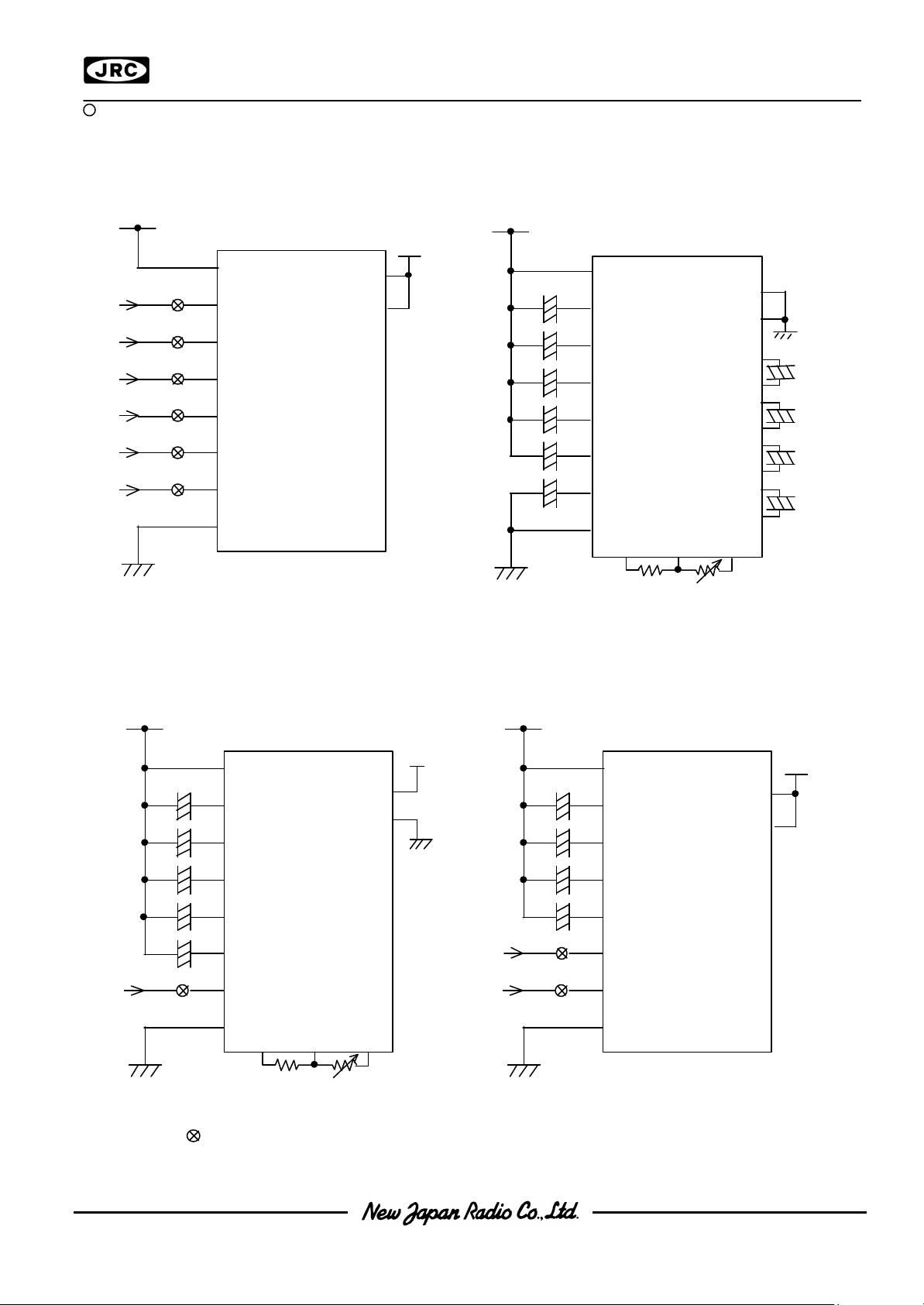
The status of internal power supply is selected by TThe status of internal power supply is selected by T11 and T and T22 terminal. Furthermore the external power supply terminal. Furthermore the external power supply
operates with some of internal power supply function.operates with some of internal power supply function.
T1 T2
L L/H ON ON ON H L OFF ON ON VOUT Open
H H OFF OFF ON V5,VOUT Open Open
When (TWhen (T11, T, T22)=(H, L), C1)=(H, L), C1++, C1, C1--, C2, C2++, C2, C2--,C3,C3++, C3, C3--, C4, C4++, C4, C4-- terminals for voltage booster circuits are open terminals for voltage booster circuits are open
because the voltage booster circuits doesn't operate. Therefore LCD driving voltage to the Vbecause the voltage booster circuits doesn't operate. Therefore LCD driving voltage to the VOUTOUT terminal terminal
should be supplied from outside.should be supplied from outside.
When (TWhen (T11, T, T22)=(H, H), terminals for voltage booster circuits and VR are open, because the voltage booster)=(H, H), terminals for voltage booster circuits and VR are open, because the voltage booster
circuits and Voltage adjust circuits do not operate.circuits and Voltage adjust circuits do not operate.
Voltage
Booster
Voltage Adj. Buffer(V/F) Ext.Pow Supply
C1+,C1- to
C4+,C 4-
VR Term.
Power Supply applicationsPower Supply applications
NJU6677NJU6677
(1)External power supply operation.(1)External power supply operation.
V
DD
V
1
V
2
V
3
V
4
V
5
V
OUT
V
SS
T1
T2
(2)Internal power supply operation.(2)Internal power supply operation.
(Voltage Booster, Voltage Adj., Buffer(V/F)) (Voltage Booster, Voltage Adj., Buffer(V/F))
Internal power supply ON (instruction) (T Internal power supply ON (instruction) (T1,1,TT22)=(L,L))=(L,L)
V
DD
+
+
+
+
+
+
V
1
V
2
V
3
V
4
V
5
V
OUT
V
SS
V
DD
V
R
T1
T2
C
1+
C
1-
C
2+
C
2-
C
3+
C
3-
C
4+
C
4-
V
5
+
+
+
+
(3)External power supply operation with(3)External power supply operation with
Voltage Adjustment,3 Buffer(V/F) Voltage Adjustment,3 Buffer(V/F)
Internal power supply ON (Instruction) (T Internal power supply ON (Instruction) (T11,T,T22) = (H,L)) = (H,L)
V
DD
+
+
+
+
+
V
V
V
V
V
V
V
1
2
3
4
5
OUT
SS
V
DDVR
T1
T2
V
5
(4)External power supply operation adjusted(4)External power supply operation adjusted
Voltage to V5. Voltage to V5.
Internal power supply (Instruction) (T Internal power supply (Instruction) (T11,T,T22) =(H,H)) =(H,H)
V
DD
+
+
+
+
V
1
V
2
V
3
V
4
V
5
V
OUT
V
SS
T1
T2
: These switches should be open during the power save mode. : These switches should be open during the power save mode.
 Loading...