

JRC NJU6631ACH Datasheet

NJU6631A
16-CHARACTER 1-LINE DOT MATRIX
LCD CONTROLLER DRIVER
GENERAL DESCRIPTION
■
NJU6631A
The
driver for up to 16-character 1-line or 8-character 2-line
display.
It contains microprocessor interface circuits,
instruction decoder controller, character generator
ROM/RAM and common and segment drivers.
The bleeder resistance generates for LCD Bias
voltage internally.
The CR oscillator incorporates C and R, therefor e no
external components for oscillation are required.
The microprocessor interface circuits which operate
2MHz frequency, can be connected directly to 4bit/8bit
microprocessor.
The character generator consists of 9,600 bits ROM
and 32 x 5 bits RAM. The standard version ROM is
coded with 192 characters including capital and small
letter fonts.
The 16-common and 40-segment drives up to 16character 1-line LCD panels which divided two comm on
electrode blocks.
The rectangle outlook is very applicable to COG or
Slim TCP.
FEATURES
■
is a 1 Chip Dot Matrix LCD controller
PRELIMINARY
PACKAGE OUTLINE
■
NJU6631ACH
●
16-character 1-line Dot Matrix LCD Controller Driver
●
4/8 Bit Microprocessor Direct Interface
●
Display Data RAM - 16 x 8 bits : Maximum 16-character 1-line Display
●
Character Generator ROM - 9,600 bits : 240 Characters for 5 x 8 Dots
●
Character Generator RAM - 32 x 5 bits : 4 Patterns(5 x 8 Dots)
●
Microprocessor can access to Display Data RAM and Character Generator RAM
●
High Voltage LCD Driver : 16-common / 40-segment
●
Duty Ratio : 1/16 Duty
●
Number of Maximum Display Characters : 16-character
●
Useful Instruction Set
Clear Display, Return Home, Display ON/OFF Cont, Cursor ON/OFF Cont, Display Blink,
Cursor Shift, Character Shift,
●
Common and Segment driver Location order Select Function(Pin configuration mode A / mode B)
●
Power On Initialize / Hardware Reset Function
●
Bleeder Resistance On-chip
●
Oscillation Circuit On-chip
●
Low Power Consumption
●
Operating Voltage --- +5V
●
Package Outline --- Bumped Chip
●
C-MOS Technology
31.Mar,2000
Ver.1
PAD LOCATION
■
NJU6631A
31
74
Y
X
Chip Size : 3.58mm x 1.68mm Bump Size : 90um x 55um
Chip Center : X=0um, Y=0um Bump Height : 17.5um TYP.
Bump Material : Au
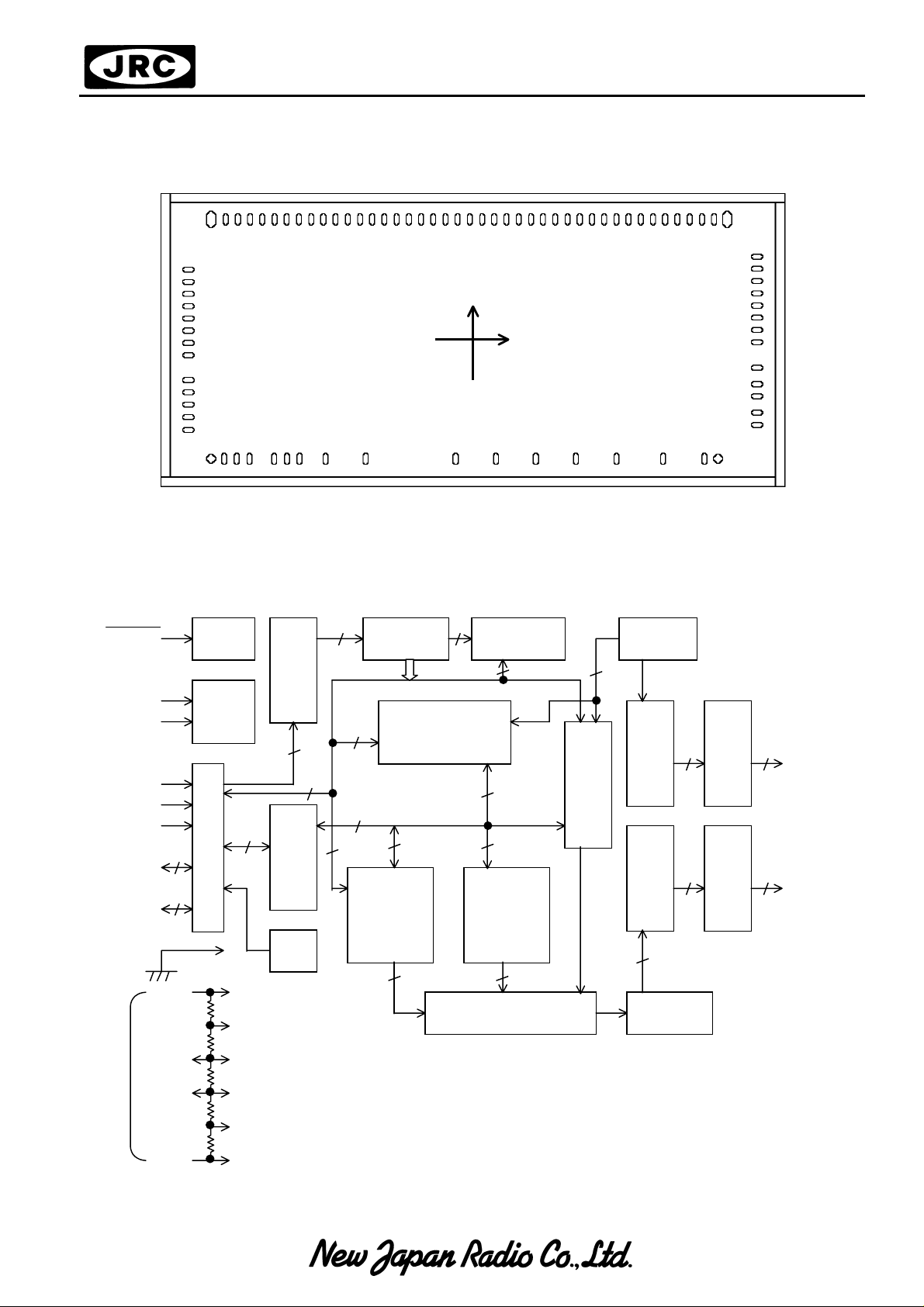
BLOCK DIAGRAM
■
RESET
OSC
OSC
1
2
DB
DB
R/W
∼DB
4
∼DB
0
RS
E
4
7
4
3
VSS
VDD
R
LCD Driver
R
V
2
R
V
3
R
R
V
5
1
Power On
Reset
CR
OSC
I/O Buffer
1
V
1
1
1
V
1
8
1
4
Instruction
Reg.(IR)
8
8
Data Reg.
(DR)
Busy
Flag
8 7
Instruction
Decoder(ID)
Address
Counter(AC)
7
Display Data RAM
7
(DD RAM)
16x8bits
8
8
5
Character
Generator
RAM
(CG RAM)
32x5bits
5
8
Character
Generator
ROM
(CG ROM)
9,600bits
5 5
Parallel to Serial
Converter
Cursor Blink
Cont.
Timing
Gen.
7
16bit
40bit
40bit
Shift Reg.
18
16 16
COM1
∼COM
Shift Reg.
Common
Driver
40 40
SEG
∼SEG
Latch
Segment
Driver
16
1
40
NJU6631A
PAD COORDINATES
■
Chip Size 3.58×1.68mm(Chip Center X=0um,Y=0um)
PAD
No.
1 Dummy1 Dummy1 -1501 -680 44 SEG12 SEG29 543 690
2 VDD V
3 VDD V
4 VDD V
5 V5 V
6 V5 V
7 V5 V
8 V3 V
9 V2 V
10 RESET RESET -98 -680 53 SEG21 SEG20 -87 690
11 RS RS 132 -680 54 SEG22 SEG19 -157 690
12 R/W R/W 361 -680 55 SEG23 SEG18 -227 690
13 E E 591 -680 56 SEG24 SEG17 -297 690
14 DB0 DB0 824 -680 57 SEG25 SEG16 -367 690
15 DB1 DB1 1091 -680 58 SEG26 SEG15 -437 690
16 DB2 DB2 1328 -680 59 SEG27 SEG14 -507 690
17 Dummy2 Dummy2 1406 -680 60 SEG28 SEG13 -577 690
18 DB3 DB3 1630 -486 61 SEG29 SEG12 -647 690
19 DB4 DB4 1630 -416 62 SEG30 SEG11 -717 690
20 DB5 DB5 1630 -322 63 SEG31 SEG10 -787 690
21 DB6 DB6 1630 -253 64 SEG32 SEG9 -857 690
22 DB7 DB7 1630 -160 65 SEG33 SEG8 -927 690
23 COM1 COM9 1630 -13 66 SEG34 SEG7 -997 690
24 COM2 COM10 1630 57 67 SEG35 SEG6 -1067 690
25 COM3 COM11 1630 127 68 SEG36 SEG5 -1137 690
26 COM4 COM12 1630 197 69 SEG37 SEG4 -1207 690
27 COM5 COM13 1630 267 70 SEG38 SEG3 -1277 690
28 COM6 COM14 1630 337 71 SEG39 SEG2 -1347 690
29 COM7 COM15 1630 407 72 SEG40 SEG1 -1417 690
30 COM8 COM16 1630 477 73 Dummy5 Dummy5 -1501 690
31 Dummy3 Dummy3 1459 690 74 COM16 COM8 -1630 402
32 Dummy4 Dummy4 1383 690 75 COM15 COM7 -1630 332
33 SEG1 SEG40 1313 690 76 COM14 COM6 -1630 262
34 SEG2 SEG39 1243 690 77 COM13 COM5 -1630 192
35 SEG3 SEG38 1173 690 78 COM12 COM4 -1630 122
36 SEG4 SEG37 1103 690 79 COM11 COM3 -1630 52
37 SEG5 SEG36 1033 690 80 COM10 COM2 -1630 -18
38 SEG6 SEG35 963 690 81 COM9 COM1 -1630 -88
39 SEG7 SEG34 893 690 82 OSC1 OSC1 -1630 -230
40 SEG8 SEG33 823 690 83 OSC2 OSC2 -1630 -300
41 SEG9 SEG32 753 690 84 VSS V
42 SEG10 SEG31 683 690 85 VSS V
43 SEG11 SEG30 613 690 86 VSS V
Note) Dummy1∼ Dummy5 are Dummy Pad.
PAD Name Center PAD Name Center
Pin Configuration Pin Configuration
Mode A Mode B
-1426 -680 45 SEG13 SEG28 473 690
DD
-1353 -680 46 SEG14 SEG27 403 690
DD
-1281 -680 47 SEG15 SEG26 333 690
DD
-1138 -680 48 SEG16 SEG25 263 690
5
-1066 -680 49 SEG17 SEG24 193 690
5
-993 -680 50 SEG18 SEG23 123 690
5
-844 -680 51 SEG19 SEG22 53 690
3
-614 -680 52 SEG20 SEG21 -17 690
2
X=(um) Y=(um)
PAD
No.
Mode A Mode B
-1630 -370
SS
-1630 -443
SS
-1630 -515
SS
X=(um) Y=(um)
TERMINAL DESCRIPTION
■
PAD No.
Pin Configuration
SYMBOL FUNCTION
Mode A Mode B
2,3,4 2,3,4 VDD Power Source (+5V)
84,85,86 84,85,86 VSS Power Source ( 0V)
9,8,
7,6,5
9,8,
7,6,5
V2,V3,
V
5
LCD Driving Power Source
Oscillation Frequency Adjust Terminals. Normally Open.
82
83
82
83
OSC1
OSC
2
For external clock operation, the clock should be input on OSC1.
(Oscillation C and R are incorporated, OSC Freq.=270kHz)
Register selection signal input
11 11 RS
“0” : Instruction Register (Writing)
Busy Flag (Reading)
“1” : Data Register (Writing/Reading)
12 12 R/W
Read/Write selection signal input
“0” : Write, “1” : Read
13 13 E Read/Write activation signal input
3-state Data Bus (Upper) to transf er the data between MPU and
22∼19 22∼19 DB
∼DB
7
4
NJU6631A
DB
is also used for the Busy flag reading.
7
3-state Data Bus (Lower) to transfer the data between MPU and
18∼14 18∼14 DB
∼DB
3
0
NJU6631A
These bus are not used in the 4-bit operation.
23∼30
81∼74
81∼74
23∼30
COM
COM
∼COM
1
∼COM
9
LCD Common driving signal Terminals
8
Common driver Location order Select as Shown in T able 4.
16
Pin configuration mode A : M0=0 / mode B : M0=1.
LCD Segment driving signal Terminals
33∼72 72∼33 SEG
∼SEG
1
Segment driver Location order Select as Shown in Table 4.
40
Pin configuration mode A : M0=0 / mode B : M0=1.
NJU6631A
10 10 RESET
Reset Terminal. W hen the “L” level input over than 1.2m s to this
terminal the system will be reset. (f
=270kHz)
OSC
NJU6631A
FUNCTIONAL DESCRIPTI O N
■
(1) Description for each blocks
(1-1) Register
NJU6631A
The
The Register (IR) stores instruction codes such as “ Clear Dis play” and “Return Home”, and address data for
Display Data RAM (DD RAM) and Character Generator RAM (CG RAM) . The MPU can write the instruction
code and address data to the Register (IR), but it cannot read out from the Register (IR).
The Register (DR) is a temporary stored register, the data stored in the Register (DR) is written into the DD
RAM or CG RAM and read out from the DD RAM or CG RAM.
The data in the Register (DR) written by the MPU is transferred automatically to the DD RAM or CG RAM by
internal operation.
When the addres s data for the DD RAM or CG RAM is written into the Register (IR) , the address ed data in
the DD RAM or CG RAM is transferred to the Register (DR). By the MPU read out the data in the Register
(DR), the data transmitting process is performed completely.
After reading the data in the Register (DR) by the MPU, the next address data in the DD RAM or CG RAM is
transferred automatically to the Register (DR) to provide for the next MPU reading.
These two registers are selected by the selection signal RS as shown below :
Table 1. shows register operation controlled by RS and R/W signals.
RS R/W Selected Register Operation
0 0 Write
0 1
1 0 Write (DR to DD RAM or CG RAM)
1 1
incorporates two 8-bit registers, an Instruction Register (IR) and a Data Register (DR).
Table 1. Register Operation
IR
DR
Read busy flag (DB
) and address counter (DB
7
Read (DD RAM or CG RAM to DR)
∼DB
0
)
6
(1-2) Busy Flag (BF)
When the internal circuits are in the operation mode, the busy flag is "1", and any instruction reading is
inhibited.
The busy flag (BF) is output at DB
when RS="0" and R/W="1" as shown in table 1.
7
The next instruction should be written after busy flag (BF) goes to "0".
(1-3) Address Counter (AC)
The address Counter (AC) addressing the DD RAM and CG RAM.
When the address setting instruction is written into the Regis ter (IR), the address inf ormation is transferred
from Register (IR) to counter (AC). The selection of either the DD RAM or CG RAM is also determ ined by this
instruction.
After writing (or reading) the display data to (or from) the DD RAM or CG RAM, the Counter (AC)
increments (or decrements) automatically.
∼DB
The address data in the Counter (AC) is output from DB
when RS="0" and R/W="1" as shown in Table
6
0
1.
(1-4) Display Data RAM (DD RAM)
The display data RAM (DD RAM) consists of 16 x 8 bits, stores up to 16-character display data represented
in 8-bit code.
The DD RAM address data set in the address Counter (AC) is represented in Hexadecimal.
Higher order bit Lower order bit (Example) DD RAM address “08”
0 0 0 1 0 0 0
AC6 AC5 AC4 AC3 AC2 AC1 AC0
AC
Hexadecimal 0 8 Hexadecimal
NJU6631A
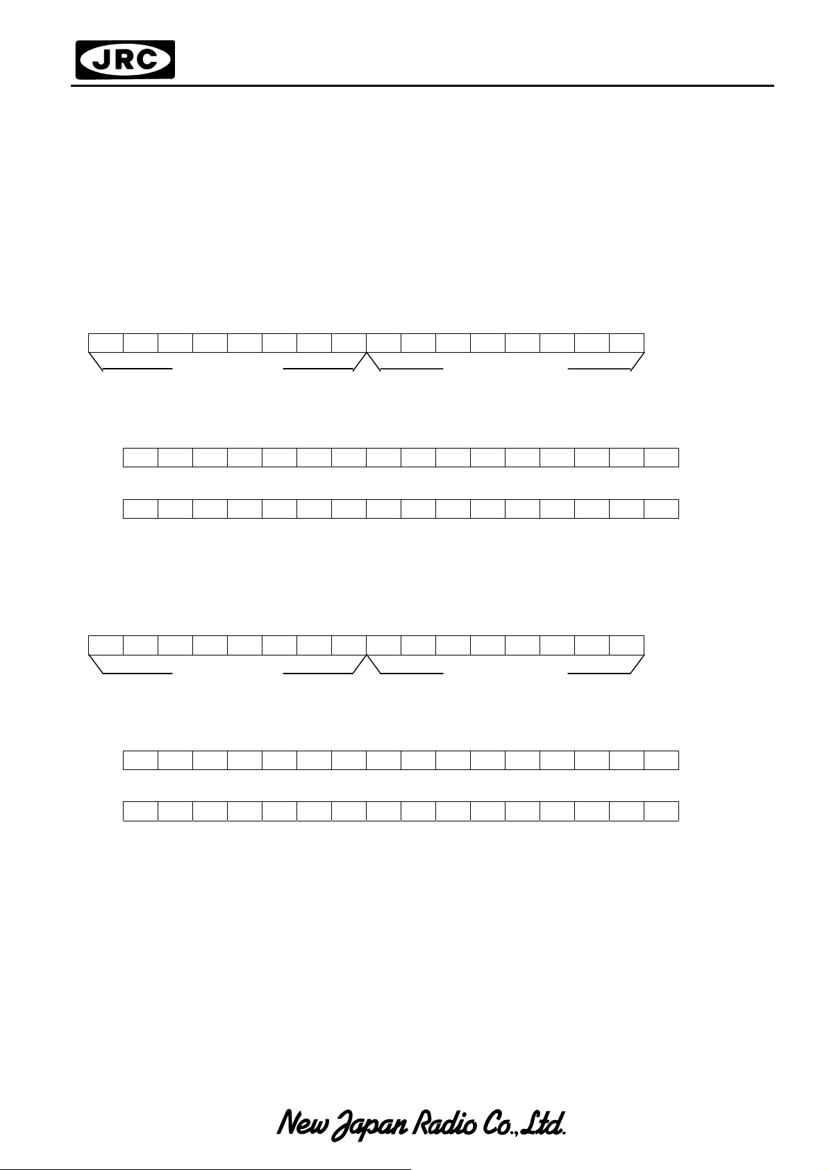
(1-4-1) 16-character 1-line Display
NJU6631A
The
which is determined by the Function Set Instruction (A= 0 and 1).
"Addressing mode 1" is using consecutive addres s of (00)
half 8-character. "Addressing mode 2" is not using consecutive addres s lik es as (00)
through (47)
16-character 1-line and 8 character 2-line are also determined by the Function Set Instruction (M1= 0 and 1) .
<Addressing mode 1: A=0, M1=0>
-The relation between DD RAM address and display position on the LCD is shown below.
has two kinds of addressing m ode called "Addressing mode 1" and "Addressing m ode 2"
through (0F)H for front half 8-c haracter and last
H
for front half 8-character and last half 8-character respectively.
H
through (07)H and (40)H
H
1 2 3 4 5 6 7 8 9 10 11 12 13 14 15 16
00 01 02 03 04 05 06 07 08 09 0A 0B 0C 0D 0E 0F
←Display position
←DD RAM address
(Hexadecimal)
∼COM
COM
1
COM
8
∼COM
9
16
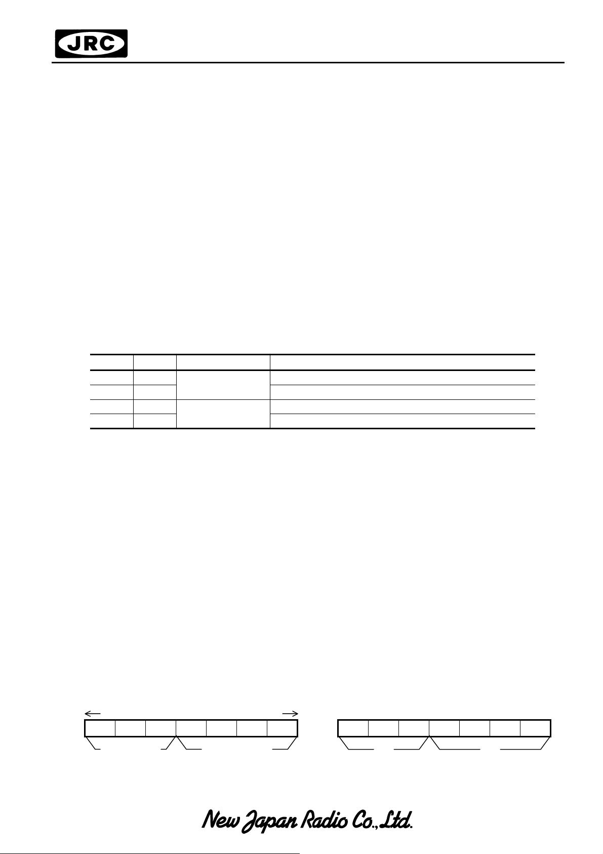
When the display shift is performed, the DD RAM address changes as follows:
(Left Shift Display)
(00)←
01 02 03 04 05 06 07 08 09 0A 0B 0C 0D 0E 0F 00
(Right Shift Display)
0F 00 01 02 03 04 05 06 07 08 09 0A 0B 0C 0D 0E
→(0F)
<Addressing mode 2: A=1, M1=0>
-The relation between DD RAM address and display position on the LCD is shown below.
1 2 3 4 5 6 7 8 9 10 11 12 13 14 15 16
00 01 02 03 04 05 06 07 40 41 42 43 44 45 46 47
←Display position
←DD RAM address
(Hexadecimal)
∼COM
COM
1
COM
8
∼COM
9
16
When the display shift is performed, the DD RAM address changes as follows:
(Left Shift Display)
(00)←
01 02 03 04 05 06 07 40 41 42 43 44 45 46 47 00
(Right Shift Display)
47 00 01 02 03 04 05 06 07 40 41 42 43 44 45 46
→(47)
(1-4-2) 8-character 2-line
2
2
<Addressing mode 1: A=0, M1=1>
-The relation between DD RAM address and display position on the LCD is shown below.
NJU6631A
1 2 3 4 5 6 7 8
COM
∼COM
1
8
1st Line 00 01 02 03 04 05 06 07
2nd Line 08 09 0A 0B 0C 0D 0E 0F
(Hexadecimal)
COM
∼COM
9
16
←Display Position
←DD RAM Address
←
When the display shift is performed, the DD RAM address changes as follows:
(Left Display Shift)
1st Line(00)←
nd Line(08)←
01 02 03 04 05 06 07 08
09 0A 0B 0C 0D 0E 0F 00
(Right Display Shift)
1st Line 0F 00 01 02 03 04 05 06
2nd Line 07 08 09 0A 0B 0C 0D 0E
→(07)
→(0F)
<Addressing mode 2: A=1, M1=1>
-The relation between DD RAM address and display position on the LCD is shown below.
1 2 3 4 5 6 7 8
COM
∼COM
1
8
1st Line 00 01 02 03 04 05 06 07
2nd Line 40 41 42 43 44 45 46 47
(Hexadecimal)
COM
∼COM
9
16
← Display Position
←DD RAM Address
←
When the display shift is performed, the DD RAM address changes as follows:
(Left Display Shift)
1st Line(00)←
nd Line(40)←
01 02 03 04 05 06 07 08
41 42 43 44 45 46 47 00
(Right Display Shift)
1st Line 47 00 01 02 03 04 05 06
2nd Line 07 40 41 42 43 44 45 46
→(07)
→(47)

NJU6631A
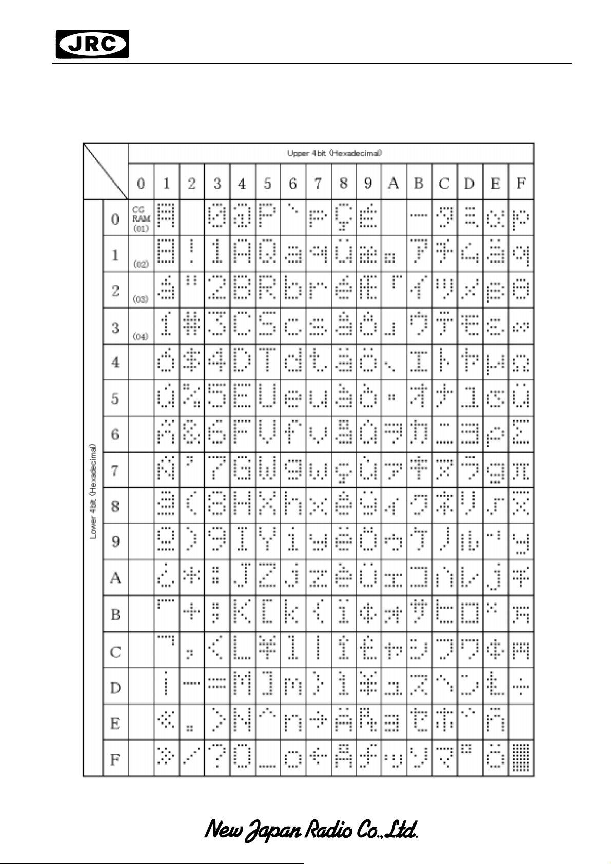
(1-5) Character Generator ROM (CG ROM)
The Character Generator ROM (CG ROM) generates 5 x 8 dots character pattern represented in 8-bit
character codes.
The storage capacity is up to 240 kinds of 5 x 8 dots character pattern. The correspondence between
character code and standard character pattern of NJU6631A is shown in Table 2.
User-defined character pattern (Custom Font) are also available by mask option.
NJU6631A
Table 2. CG ROM Character Pattern (ROM version -02)
→
NJU6631A
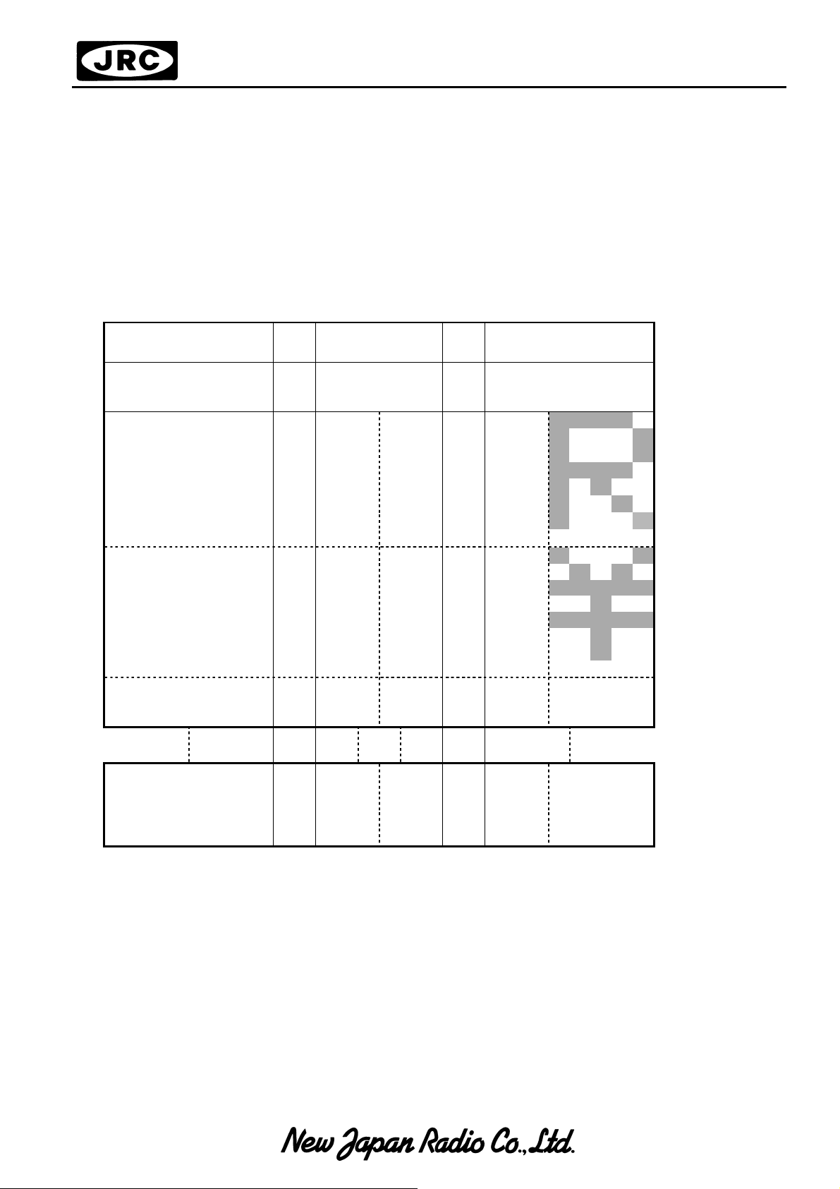
(1-6) Character Generator RAM (CG RAM)
The character generator RAM (CG RAM) can s tore any kinds of character pattern in 5 x 7 dots written by
the user program to display user’s original character patter n. The CG RAM can stor e 4 kinds of c haracter in 5
x 7 dots mode.
To display user ’s original c haracter pattern stor ed in the CG RAM, the address data (00)
written to the DD RAM as shown in Table 2.
Table 3. shows the correspondence among the character pattern, CG RAM address and Data.
Table 3. Correspondence of CG RAM address, DD RAM character code
and CG RAM character pattern (5 x 7 dots).
Character Code
(DD RAM Data)
7 6 5 4 3 2 1 0 4 3 2 1 0 4 3 2 1 0
Upper bit Lower bit
0 0 0 0 * * 0 0 0 0 1 0 0 1 0 1 0 0 Character Pattern
0 0 0 0 * * 0 1 0 1 1 0 0 1 1 1 1 1 Character Pattern
* : Don’t Care
→ ←
CG RAM Address
Upper bit Lower bit
0 0 0 1 1 1 1 0
0 0 1 1 0 0 0 1
0 1 0 1 0 0 0 1
0 1 1
1 0 1 1 0 0 1 0 Example (1)
1 1 0 1 0 0 0 1
1 1 1
0 0 0 1 0 0 0 1
0 0 1 0 1 0 1 0
0 1 0 1 1 1 1 1
0 1 1 0 0
1 0 1 0 0 1 0 0 Example (2)
1 1 0 0 0 1 0 0
1 1 1
0 0 0
0 0 1
→ ←
Character Pattern
(CG RAM Data)
Upper bit Lower bit
1 1 1 1 0
0 0 0 0 0
1 0 0
0 0 0 0 0
∼ (03)H should be
H
←Cursor Position
←Cursor Position
0 0 0 0 * * 1 1 1 1
Notes : 1.Character code bits 0 to 1 correspond to the CG RAM address 3 and 4 (2 bits : 4 patterns)
2.CG RAM address 0, 1 and 2 designate character pattern Line position.
The 8th line is the cursor position and the dis play is perfor m ed by logical O R with c ursor. Therefor e,
in case of the cursor dis play, the 8th line should be "0". If ther e is "1" in the 8th line, the bit "1" is
always displayed on the cursor position regardless of cursor existence.
3.Character pattern row position correspond to the CG RAM data bits 0 to 4 are shown above.
The bits 5 to 7 of the CG RAM do not exist.
4.CG RAM character patterns are selected when character code bits 4 to 7 are all "0" and it is
addressed by character code bits 0 to 1. Theref ore, the addres s (00)
the same character pattern as shown in Table 2 and Table 3.
5."1" for CG RAM data corresponds to display On and "0" to display Off.
1 0 0
1 0 1
1 1 0
1 1 1
, (04)H, (08)H and (0C)H, select
H
 Loading...