

JRC NJU6624BFG1, NJU6624AFG1 Datasheet
12-CHARACTER 1-LINE DOT MATRIX LCD12-CHARACTER 1-LINE DOT MATRIX LCD
CONTROLLER DRIVER with SMOOTH SCROLL FUNCTIONCONTROLLER DRIVER with SMOOTH SCROLL FUNCTION
The NJU6624A/B is a Dot Matrix LCD controller driver for 12-characterThe NJU6624A/B is a Dot Matrix LCD controller driver for 12-character
1-line with icon display in single chip.1-line with icon display in single chip.
It contains bleeder resistance, general output port, keyscan circuit,It contains bleeder resistance, general output port, keyscan circuit,
CR oscillator, microprocessor interface circuit, instruction decoder con-CR oscillator, microprocessor interface circuit, instruction decoder controller, character generator ROM/RAM, high voltage operation com-troller, character generator ROM/RAM, high voltage operation common and segment drivers, and others.mon and segment drivers, and others.
The character generator ROM consisting of 7,840 bits stores 224 kindsThe character generator ROM consisting of 7,840 bits stores 224 kinds
of character Font. Each 1,120 bits CG RAM and Icon display RAMof character Font. Each 1,120 bits CG RAM and Icon display RAM
can store 32 kinds of special character displayed on the dot matrixcan store 32 kinds of special character displayed on the dot matrix
display area or 60 kinds of Icon on the Icon display area.display area or 60 kinds of Icon on the Icon display area.
The 8-common (7 for character, 1 for icon) and 71-segment driversThe 8-common (7 for character, 1 for icon) and 71-segment drivers
operate 12-character 1-line with 60 Icon LCD display and LED driveroperate 12-character 1-line with 60 Icon LCD display and LED driver
drives 4 LED which can use like as indicator.drives 4 LED which can use like as indicator.
The 16th display contrast control function is incorporated. Therefore,The 16th display contrast control function is incorporated. Therefore,
the contrast adjustment is operated easily by only simple power sup-the contrast adjustment is operated easily by only simple power supply circuit on-chip.ply circuit on-chip.
The complete CR oscillator requires no external components.The complete CR oscillator requires no external components.
The serial interface which operates by 1MHz, communicates with ex-The serial interface which operates by 1MHz, communicates with external MCU.ternal MCU.
As an outstanding feature, NJU6624A/B realizes the horizontal smoothAs an outstanding feature, NJU6624A/B realizes the horizontal smooth
scroll of characters by combination of instructions.scroll of characters by combination of instructions.
The combination of NJU6624A as the Master and NJU6624B as theThe combination of NJU6624A as the Master and NJU6624B as the
slave drive the 12-character and 2-line LCD panel or 24-character 1-slave drive the 12-character and 2-line LCD panel or 24-character 1line in 1/8 duty.line in 1/8 duty.
NJU6624A/BNJU6624A/B
PRELIMINARYPRELIMINARY
ggPACKAGE OUTLINEPACKAGE OUTLINEggGENERAL DESCRIPTIONGENERAL DESCRIPTION
NJU6624A/BFG1NJU6624A/BFG1
ggFEATURESFEATURES
12-character 1-line Dot Matrix LCD Controller Driver 12-character 1-line Dot Matrix LCD Controller Driver
nn
Maximum 60 Icon Display Maximum 60 Icon Display
nn
Serial Direct Interface with Microprocessor Serial Direct Interface with Microprocessor
nn
Display Data RAM Display Data RAM - 14 x 8 bits- 14 x 8 bits : Maximum 12-character 1-line Display: Maximum 12-character 1-line Display
nn
Character Generator ROM Character Generator ROM - 7,840 bits- 7,840 bits : 224 Characters for 5 x 7 Dots: 224 Characters for 5 x 7 Dots
nn
Character Generator RAM Character Generator RAM - 1,120 bits- 1,120 bits : 32 Patterns( 5 x 7 Dots ): 32 Patterns( 5 x 7 Dots )
nn
Icon Display RAM Icon Display RAM - Maximum 60 Icons- Maximum 60 Icons
nn
High Voltage LCD Driver High Voltage LCD Driver : 8-common / 71-segment: 8-common / 71-segment
nn
Duty and Bias Ratio Duty and Bias Ratio : 1/8 duty, 1/4 bias: 1/8 duty, 1/4 bias
nn
Master/Slave Function Master/Slave Function :NJU6624A : Master, NJU6624B : Slave:NJU6624A : Master, NJU6624B : Slave
nn
Useful Instruction Set Useful Instruction Set : Clear Display, Address Home, Display ON/OFF Cont., Display Blink,: Clear Display, Address Home, Display ON/OFF Cont., Display Blink,
nn
Address Shift, Character Shift, Dot shift, Keyscan ON/OFF Cont. e.t.c. Address Shift, Character Shift, Dot shift, Keyscan ON/OFF Cont. e.t.c.
32Key Input (4x8 keyscan) 32Key Input (4x8 keyscan)
nn
G General output port (4 ports)eneral output port (4 ports)
nn
Power On Initialization / Hardware Reset Power On Initialization / Hardware Reset
nn
Bleeder Resistance on-chip Bleeder Resistance on-chip
nn
Software contrast control(16 step) Software contrast control(16 step)
nn
Oscillation Circuit on-chip Oscillation Circuit on-chip
nn
Low Power Consumption Low Power Consumption
nn
Operating Voltage --- 2.4 to 5.5 V Operating Voltage --- 2.4 to 5.5 V
nn
Package Outline --- QFP 100 Package Outline --- QFP 100
nn
C-MOS Technology C-MOS Technology
nn
Mar.2000Mar.2000
Ver.1 Ver.1
ggPIN CONFIGURATIONPIN CONFIGURATION
NJU6624A/BNJU6624A/B
VLCD1
VDD
OSC1
REQ
DATA
SCL
CS
RESET
VSS
SEG1/S0
SEG2/S1
SEG3/S2
SEG4/S3
SEG5/S4
SEG6/S5
SEG7/S6
SEG8/S7
V1
VLCD 2
1
P0
P1
P2
P3
K0
K1
K2
K3
C OM 7
C OM MK
V2
V4
C OM 3
C OM 4
C OM 6
C OM 5
NJU6624A/BFG1
SEG70
SEG69
SEG67
SEG68
SEG66
SEG65
SEG63
SEG64
SEG62
SEG61
SEG60
C OM 1
C OM 2
SEG71
SEG59
SEG58
SEG57
SEG56
SEG55
SEG54
SEG53
SEG52
SEG51
SEG50
SEG49
SEG48
SEG47
SEG46
SEG45
SEG44
SEG43
SEG42
SEG41
SEG40
SEG39
SEG38
SEG37
SEG36
SEG35
SEG34
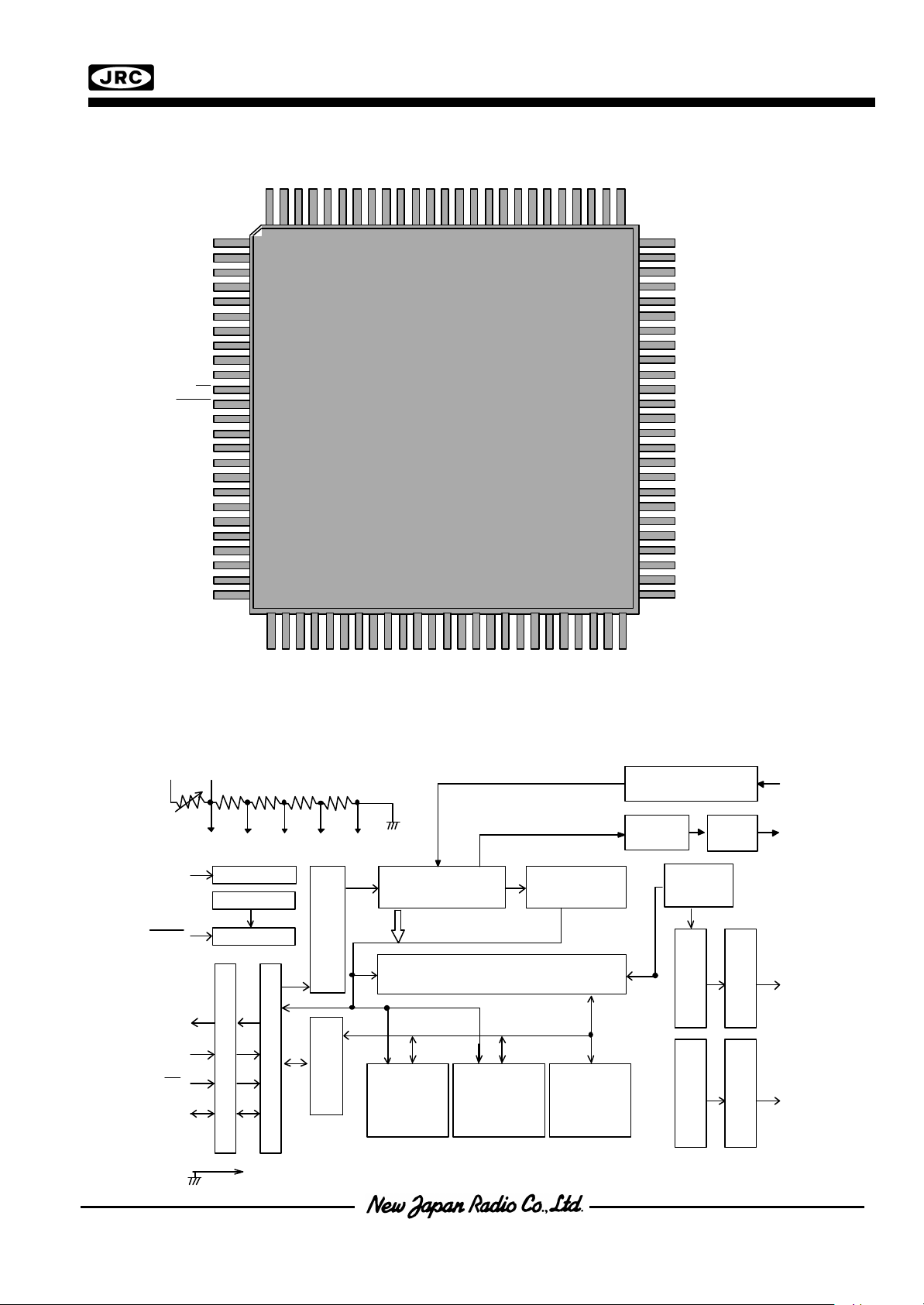
ggBLOCK DIAGRAMBLOCK DIAGRAM
V
V
0SC1
RESET
LCD1
REQ
SCL
CS
DATA
LCD2
V
LCD
SEG9
RBRB
V
1
CR OSC Circui t
Power On Reset
Reset
I/ O B u ff e r
Seri al t o Pa ra ll e l Co nvertor
V
(V3)
SEG10
SEG11
SEG13
SEG12
SEG14
SEG15
SEG17
SEG16
SEG18
SEG19
SEG20
SEG22
SEG21
RB
RB
V
2
V
4
SS
Instru ct ion
Decode r(ID )
R e g i st e r(I R)
Display
Instr uction
Icon Display
R e gi s te r( IR )
D a t a
RAM
(MK RAM)
12x5bits
Data RAM (DD RAM)
14x8bits
Character
Generator
(CG RAM)
5x7x32bits
SEG23
SEG24
RAM
SEG25
SEG26
SEG27
Address
SEG28
SEG29
SEG30
Counte r
Character
Generator
ROM
(CG ROM)
7,840bits
SEG32
SEG33
SEG31
Key scan Circuit
LED port
Register
Output
Buffer
K0 to K3
P0 to P3
Timing
Gen.
COM1
to COM7
Dri v er
Shift R e g .
8 bit
C o mm o n
Latch
71bi t
Se gment
/COMMK
D riv e r
SEG
1
to SEG
71
V
SS
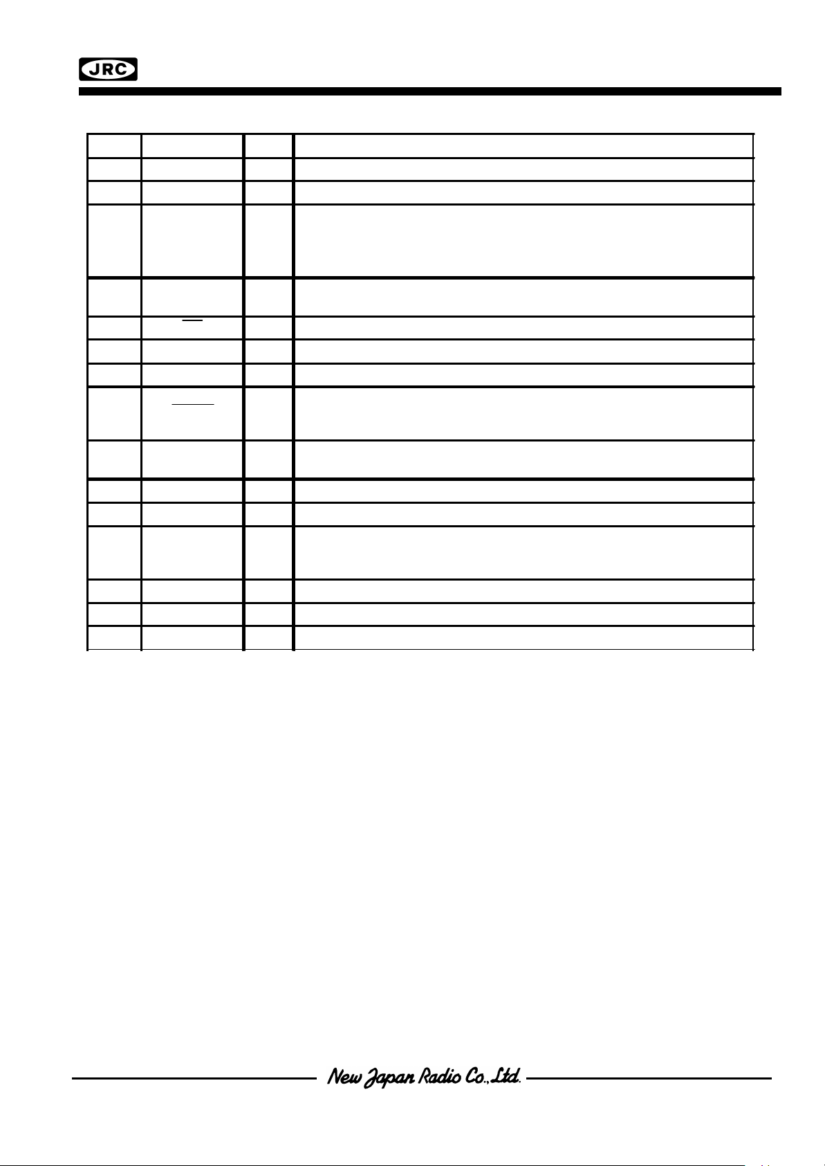
ggTERMINAL DESCRIPTIONTERMINAL DESCRIPTION
No. SYMBOL I/O F U N C T I O N
2,13 VDD,VSS - Power Source:VDD=+5V,GND:VSS=0V
1 VLCD1 I LCD driving voltage input terminal
NJU6624A/BNJU6624A/B
100
99
98
97
3 OSC1 I
11 CS I Chip select signal input of serial I/F.
10 SCL I Sift clock input of serial I/F.
9 DATA I Serial Data Input of serial I/F.
12 RESET I
4-7 P0-P3 O
8 REQ O Key request signal output terminal.
14-17 K0-K3 I Key scanning input terminals.
18-25
26-88 SEG 9-SEG71 O LCD segment driving signal output terminals
89-95 COM1-COM7 O LCD common driving signal output terminals
VLCD2
V1
V2
V4
SEG 1/S0
-
SEG 8/S7
LCD driving voltage stabilization capacitor terminals.
Connect the capacitor between VLCD2 and VSS, V1 and VSS, V2 and
I
VSS, V4 and VSS.
typ. : 0.1uF
System clock input terminal
This terminal should be open for internal clock operation.
Reset Terminal.
When the "L" level is input over than 1.2ms to this terminal,
the system will be reset ( at fOSC 145KHz ).
General output port
LED driver drives LED as indicator on athers.
O LCD segment driving signal output / Key scanning output terminals.
96 COMMK O Icon common driving signal output terminals
ggFUNCTIONAL DESCRIPTIONFUNCTIONAL DESCRIPTION
(1-1)Register(1-1)Register
The NJU6624A/B incorporates two 8-bit registers, an Instruction Register(IR) and a Data Register(DR). TheThe NJU6624A/B incorporates two 8-bit registers, an Instruction Register(IR) and a Data Register(DR). The
Register (IR) stores instruction codes such as "Clear Display" and "Cursor Shift" or address data for Display DataRegister (IR) stores instruction codes such as "Clear Display" and "Cursor Shift" or address data for Display Data
RAM(DD RAM), Character Generator RAM(CG RAM) and Icon Display RAM (MK RAM).RAM(DD RAM), Character Generator RAM(CG RAM) and Icon Display RAM (MK RAM).
The Register(DR) is a temporary register, the data in the Register(DR) is written into the DD RAM, CG RAM orThe Register(DR) is a temporary register, the data in the Register(DR) is written into the DD RAM, CG RAM or
MK RAM.MK RAM.
The data in the Register(DR) written by the MPU is transferred automatically to the DD RAM, CG RAM or MKThe data in the Register(DR) written by the MPU is transferred automatically to the DD RAM, CG RAM or MK
RAM by internal operation.RAM by internal operation.
These two registers are selected by the selection signal RS as shown below.These two registers are selected by the selection signal RS as shown below.
(1-2)Address Counter (AC)(1-2)Address Counter (AC)
The address counter(AC) addresses the DD RAM, CG RAM or MK RAM.The address counter(AC) addresses the DD RAM, CG RAM or MK RAM.
When the address setting instruction is written into the Register(IR), the address information is transferred fromWhen the address setting instruction is written into the Register(IR), the address information is transferred from
Register(IR) to the Counter(AC). The selection of either the DD RAM, CG RAM or MK RAM is also determined byRegister(IR) to the Counter(AC). The selection of either the DD RAM, CG RAM or MK RAM is also determined by
this instruction.this instruction.
After writing (or reading) the display data to (or from) the DD RAM, CG RAM or MK RAM, the Counter(AC) incre-After writing (or reading) the display data to (or from) the DD RAM, CG RAM or MK RAM, the Counter(AC) increments (or decrements) automatically.ments (or decrements) automatically.
(1-3)Display Data RAM (DD RAM)(1-3)Display Data RAM (DD RAM)
The display data RAM (DD RAM) consist of 14x 8 bits stores up to 14-character display data represented in 8-bitThe display data RAM (DD RAM) consist of 14x 8 bits stores up to 14-character display data represented in 8-bit
code. (2 out of the 14characters are used for scroll RAM.)code. (2 out of the 14characters are used for scroll RAM.)
The DD RAM address data set in the address counter(AC) is represented in Hexadecimal.The DD RAM address data set in the address counter(AC) is represented in Hexadecimal.
NJU6624A/BNJU6624A/B
Higher Lower
AC AC4 AC3 AC2 AC1 AC0
HEX.HEX.
The relation between DD RAM address and display position on the LCD is shown below.The relation between DD RAM address and display position on the LCD is shown below.
1 2 3 4 5 6 7 8 9 10 11 12 13 14 -Display Position
00 01 02 03 04 05 06 07 08 09 0A 0B 0C 0D
When the display shift is performed,the DD RAM address changes as follows:When the display shift is performed,the DD RAM address changes as follows:
( Left Shift Display )( Left Shift Display )
(00)<= 01 02 03 04 05 06 07 08 09 0A 0B 0C 0D 00
( Right Shift Display )( Right Shift Display )
0D 00 01 02 03 04 05 06 07 08 09 0A 0B 0C =>(0E)
(Example) DD RAM address " 08 "(Example) DD RAM address " 08 "
0 1 0 0 0
00
-DD RAM Address (Hex.)
| | Scroll RAM | | Scroll RAM
88
((1-4)Character Generator ROM (CG ROM)1-4)Character Generator ROM (CG ROM)
The Character Generator ROM (CG ROM) generates 5 x 7 dots character pattern represented in 8-bit characterThe Character Generator ROM (CG ROM) generates 5 x 7 dots character pattern represented in 8-bit character
code.code.
The storage capacity is up to 224 kinds of 5 x 7 dots character pattern(available address is (20)The storage capacity is up to 224 kinds of 5 x 7 dots character pattern(available address is (20)HH through (FF) through (FF)HH).).
The correspondence between character code and standard character pattern of NJU6624A/B is shown in Table 2.The correspondence between character code and standard character pattern of NJU6624A/B is shown in Table 2.
User-defined character patterns (Custom Font) are also available by mask option.User-defined character patterns (Custom Font) are also available by mask option.
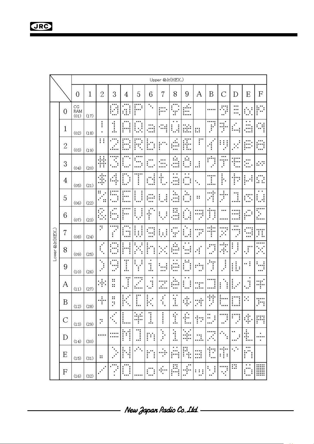
Table 2. CG ROM Character Pattern ( ROM version -02 )Table 2. CG ROM Character Pattern ( ROM version -02 )
NJU6624A/BNJU6624A/B
NJU6624A/BNJU6624A/B
(1-5)Character Generator RAM ( CG RAM )(1-5)Character Generator RAM ( CG RAM )
The character generator RAM ( CG RAM ) can store any kind of character pattern in 5 x 7 dots written by the userThe character generator RAM ( CG RAM ) can store any kind of character pattern in 5 x 7 dots written by the user
program to display user's original character pattern. The CG RAM can store 32 kind of character in 5 x 7 dotsprogram to display user's original character pattern. The CG RAM can store 32 kind of character in 5 x 7 dots
mode.mode.
To display user's original character pattern stored in the CG RAM, the address data (00)To display user's original character pattern stored in the CG RAM, the address data (00)HH-(1F)-(1F)HH should be written should be written
to the DD RAM as shown in Table 2.to the DD RAM as shown in Table 2.
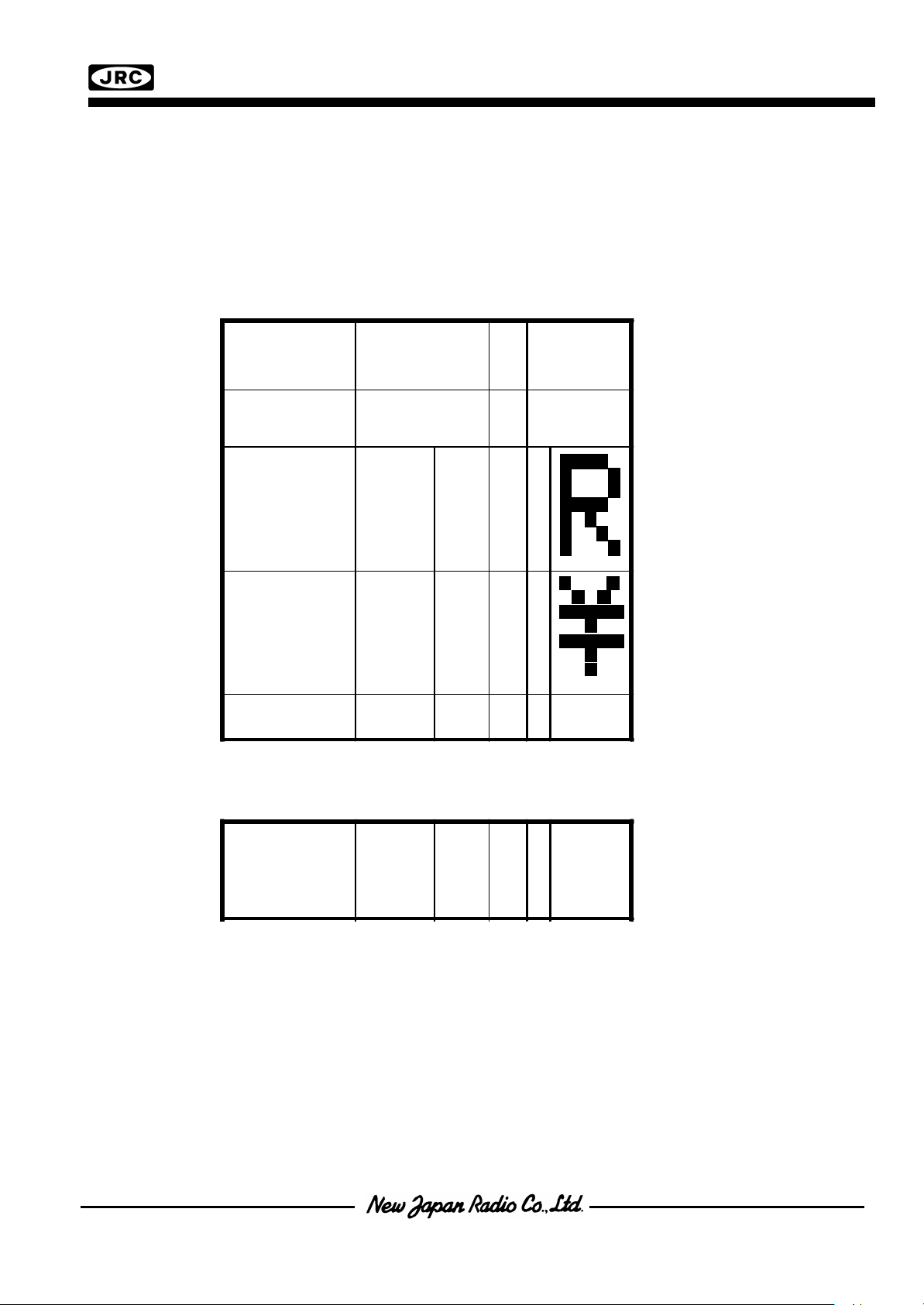
Table 3. shows the correspondence among the character pattern, CG RAM address and Data.Table 3. shows the correspondence among the character pattern, CG RAM address and Data.
Table 3. Correspondence of CG RAM address, DD RAM character codeTable 3. Correspondence of CG RAM address, DD RAM character code
and CG RAM character pattern( 5 x 7 dots ) and CG RAM character pattern( 5 x 7 dots )
Character Code
(DD RAM Data)
7 6 5 4 3 2 1 0
Upperbit Lower bit
CG RAM Address
7 6 5 4 3 2 1 0
Upperbit Lower bit
0 0 0 0 0 0 0 0 0 0 0 0 0
0 0 0 0 0 0 0 1 0 0 0 0 1
.
.
.
.
.
.
.
.
.
.
0 0 0 1 1 1 1 1 1 1 1 1 1
0 0 0
0 0 1
0 1 0
0 1 1
1 0 0
1 0 1
1 1 0
1 1 1
0 0 0
0 0 1
0 1 0
0 1 1
1 0 0
1 0 1
1 1 0
1 1 1
0 0 0
0 0 1
.
.
.
.
.
Character
Pattern
(CG RAM
Data)
4 3 2 1 0
Upper Lower
bit bi t
1 1 1 1 0
1 0 0 0 1
1 0 0 0 1
1 1 1 1 0
1 0 1 0 0
1 0 0 1 0
1 0 0 0 1
* * * * *
1 0 0 0 1
0 1 0 1 0
1 1 1 1 1
0 0 1 0 0
1 1 1 1 1
0 0 1 0 0
0 0 1 0 0
* * * * *
.
.
.
.
.
Character Pattern
Example(1)
<= Cursor Position
Character Pattern
Example(2)
<= Cursor Position
*=Don't care*=Don't care
1 0 0
1 0 1
1 1 0
1 1 1
Notes :Notes : 1. Character code bit 0 to 4 correspond to the CG RAM address bit 3 to 7(5bits:32 patterns).1. Character code bit 0 to 4 correspond to the CG RAM address bit 3 to 7(5bits:32 patterns).
2. CG RAM address 0 to 2 designate character pattern line position. The 8th line is Don't care line.2. CG RAM address 0 to 2 designate character pattern line position. The 8th line is Don't care line.
In case of input CG RAM data continuously, invalid address are Cursor position automatically. In case of input CG RAM data continuously, invalid address are Cursor position automatically.
3. Character pattern row position correspond to the CG RAM data bits 0 to 4 are shown above.3. Character pattern row position correspond to the CG RAM data bits 0 to 4 are shown above.
4. CG RAM character patterns are selected when character code of DD RAM bits 5 to 7 are all "0"4. CG RAM character patterns are selected when character code of DD RAM bits 5 to 7 are all "0"
and these are addressed by character code bits 0 and 1. and these are addressed by character code bits 0 and 1.
5. "1" for CG RAM data corresponds to display On and "0" to display Off.5. "1" for CG RAM data corresponds to display On and "0" to display Off.
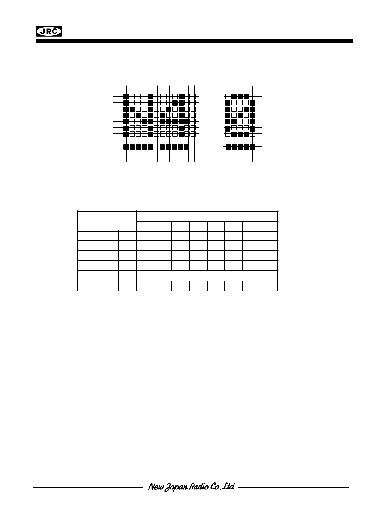
(1-6)Icon Display RAM (MK RAM)(1-6)Icon Display RAM (MK RAM)
The NJU6624A/B can display maximum 60 Icons.The NJU6624A/B can display maximum 60 Icons.
The Icon Display can be controlled by writing the Data in MK RAM corresponds to the Icon.The Icon Display can be controlled by writing the Data in MK RAM corresponds to the Icon.
The relation between MK RAM address and Icon Display position is shown below:The relation between MK RAM address and Icon Display position is shown below:
NJU6624A/BNJU6624A/B
COM1COM1
COM2COM2
COM3COM3
COM4COM4
COM5COM5
COM6COM6
COM7COM7
COMMKCOMMK
SEG SEG 1 2 3 4 5 6 7 8 91 2 3 4 5 6 7 8 9 10 11 12 10 11 12 - - - -- - - - 6 6 767686970718697071
Table 4. Correspondence among Icon Position, MK RAM Address and DataTable 4. Correspondence among Icon Position, MK RAM Address and Data
MK RAM Address
(10H-1BH)
1 0000 10H 0 0 0 "1" "2" "3" "4" "5"
1 0001 11 H 0 0 0 "5" "7" "8" "9" "10"
1 0010 12
1 0011 13H 0 0 0 "16" "17" "18" "19" "20"
: :
1 1011 1BH 0 0 0 "56" "57" "58" "59" "60"
11
Bits for Icon Display Position
D 7 D6 D5 D4 D3 D2 D1 D0
0 0 0 "11" "12" "13" "14" "15"
H
- - - - - - - -
- - - - - - - -
- - - - - - - -
- - - - - - - -
- - - - - - - -
- - - - - - - -
- - - - - - - -
- - - - - - - -
:
6060
NotesNotes :There is no icon, on the segment terminals which are six times number of tines. (6th, 12th, 18th, 24th.... ):There is no icon, on the segment terminals which are six times number of tines. (6th, 12th, 18th, 24th.... )
(1-7)Timing Generator(1-7)Timing Generator
The timing generator generates a timing signals for the DD RAM, CG RAM and MK RAM and other internalThe timing generator generates a timing signals for the DD RAM, CG RAM and MK RAM and other internal
circuits.circuits.
RAM read timing for the display and internal operation timing for MPU access are separately generated, so thatRAM read timing for the display and internal operation timing for MPU access are separately generated, so that
they may not interfere with each other.they may not interfere with each other.
Therefore, when the data write to the DD RAM for example, there will be no undesirable influence, such as flicker-Therefore, when the data write to the DD RAM for example, there will be no undesirable influence, such as flickering, in areas other than the display area.ing, in areas other than the display area.
(1-8)LCD Driver(1-8)LCD Driver
LCD Driver consists of 8-common driver and 71-segment driver.LCD Driver consists of 8-common driver and 71-segment driver.
The character pattern data are latched to the addressed Segment-register respectively. This latched data controlsThe character pattern data are latched to the addressed Segment-register respectively. This latched data controls
display driver to output LCD driving waveform.display driver to output LCD driving waveform.
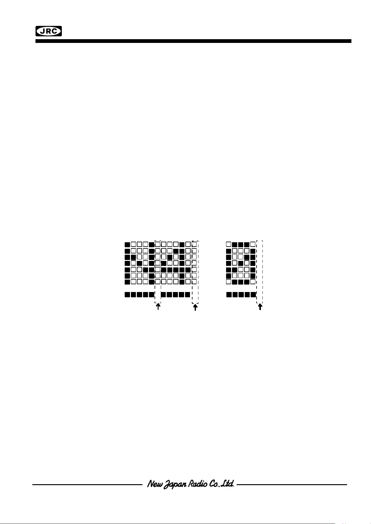
Note) DisplayNote) Display
The NJU6624A/B generate “SPACE” automatically on the segment terminals. Which are six times number ofThe NJU6624A/B generate “SPACE” automatically on the segment terminals. Which are six times number of
lines, regardless the smooth scroll function. In busy of the smooth scroll operation, this “SPACE” scrolls also withlines, regardless the smooth scroll function. In busy of the smooth scroll operation, this “SPACE” scrolls also with
characters, there is no icon on the segment terminals which are six times number of lines.characters, there is no icon on the segment terminals which are six times number of lines.
NJU6624A/BNJU6624A/B
COM1COM1
COM2COM2
COM3COM3
COM4COM4
COM5COM5
COM6COM6
COM7COM7
COMMKCOMMK
SEG SEG 1 2 3 4 5 6 7 8 91 2 3 4 5 6 7 8 910 11 12 10 11 12 - - - - - - - - 6 6767686970718697071
“SPACE” is generated when data“SPACE” is generated when data
read out from CGROM or CGRAMread out from CGROM or CGRAM
- - - - - - - -
- - - - - - - -
- - - - - - - -
- - - - - - - -
- - - - - - - -
- - - - - - - -
- - - - - - - -
- - - - - - - -
The loot number ofThe loot number of
segment is 71, so thatsegment is 71, so that
“SPACE” is not here.“SPACE” is not here.
NJU6624A/BNJU6624A/B
(1-9)Keyscan circuit(1-9)Keyscan circuit
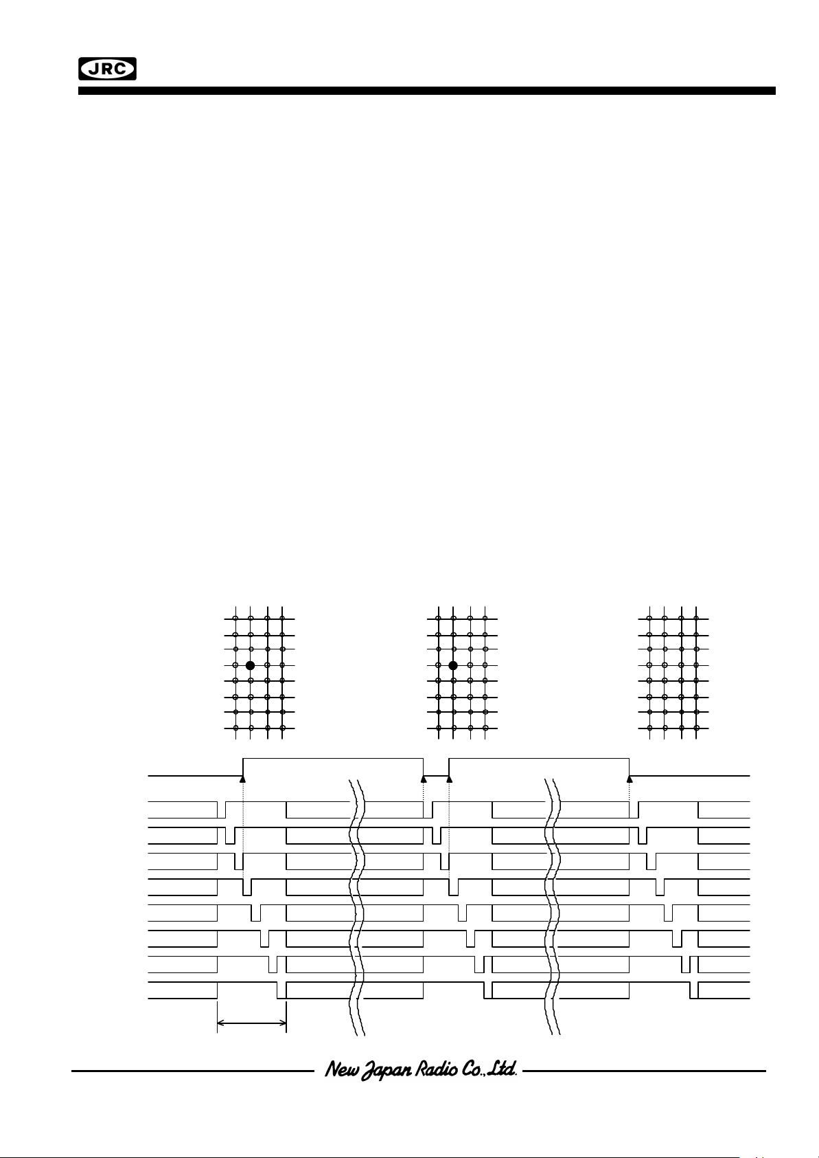
The Keyscan circuit consists of a detector block of key pressing and a fetching block of key status. It scans 4x8The Keyscan circuit consists of a detector block of key pressing and a fetching block of key status. It scans 4x8
key matrix and fetches conditions of 32 keys. Furthermore, it operates correctly against the key roll over input.key matrix and fetches conditions of 32 keys. Furthermore, it operates correctly against the key roll over input.
-Request signal output-Request signal output
When the NJU6624A/B detect the key-in by the key scan circuit, it outputs “H” signal as the request signal fromWhen the NJU6624A/B detect the key-in by the key scan circuit, it outputs “H” signal as the request signal from
the “REQ” terminal to notice the key pressing information to an application system.the “REQ” terminal to notice the key pressing information to an application system.
The request signal resets to “L” level before 2 clock of next scanning.The request signal resets to “L” level before 2 clock of next scanning.
-Contents of key register renewal-Contents of key register renewal
Contents of key register are “0000 0000” in case of no key operation. Contents of key register are not changed inContents of key register are “0000 0000” in case of no key operation. Contents of key register are not changed in
busy of key data reading operation. Key data is fetched into the key register after 2 clock of the end of a keyscanbusy of key data reading operation. Key data is fetched into the key register after 2 clock of the end of a keyscan
cycle and kept by the start of next cycle.cycle and kept by the start of next cycle.
-Key data input terminal and segment terminal-Key data input terminal and segment terminal
Keyscan signal output terminals operate as segment terminals (SEG1 to SEG8) also and keyscan signals areKeyscan signal output terminals operate as segment terminals (SEG1 to SEG8) also and keyscan signals are
output in interval period of segment signals. Key data input terminals (K0 to K3) are pulled up to VDD in busy ofoutput in interval period of segment signals. Key data input terminals (K0 to K3) are pulled up to VDD in busy of
keyscan operation (tKS). In this period, terminals of SEG9 to SEG71 output the voltage of V2 or Vkeyscan operation (tKS). In this period, terminals of SEG9 to SEG71 output the voltage of V2 or VLCD2LCD2..
-Keyscan OFF mode-Keyscan OFF mode
Keyscan operation is turned ON or OFF by the instruction. In case of keyscan OFF, the detector of key pressingKeyscan operation is turned ON or OFF by the instruction. In case of keyscan OFF, the detector of key pressing
is not operating and key data input terminals (K0 to K3) are not pulled up during the period of keyscan (tKS). Inis not operating and key data input terminals (K0 to K3) are not pulled up during the period of keyscan (tKS). In
the period of keyscan (tKS), all of segment terminals (SEG1 to SEG71) output the voltage of V2 or Vthe period of keyscan (tKS), all of segment terminals (SEG1 to SEG71) output the voltage of V2 or VLCD2LCD2..
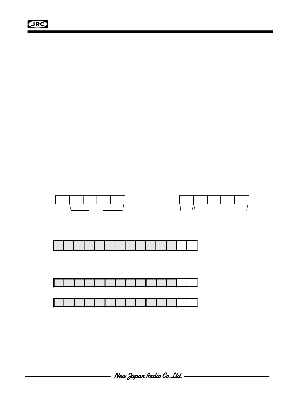
-Example Keyscan-Example Keyscan
S0
S1
S2
S3
S4
S5
S6
S7
S0
S1
S2
S3
S4
S5
S6
S7
S0
S1
S2
S3
S4
S5
S6
S7
REQREQ
SEG1/S0SEG1/S0
SEG2/S1SEG2/S1
SEG3/S2SEG3/S2
SEG4/S3SEG4/S3
SEG5/S4SEG5/S4
SEG6/S5SEG6/S5
SEG7/S6SEG7/S6
SEG8/S7SEG8/S7
tKStKS
NJU6624A/BNJU6624A/B
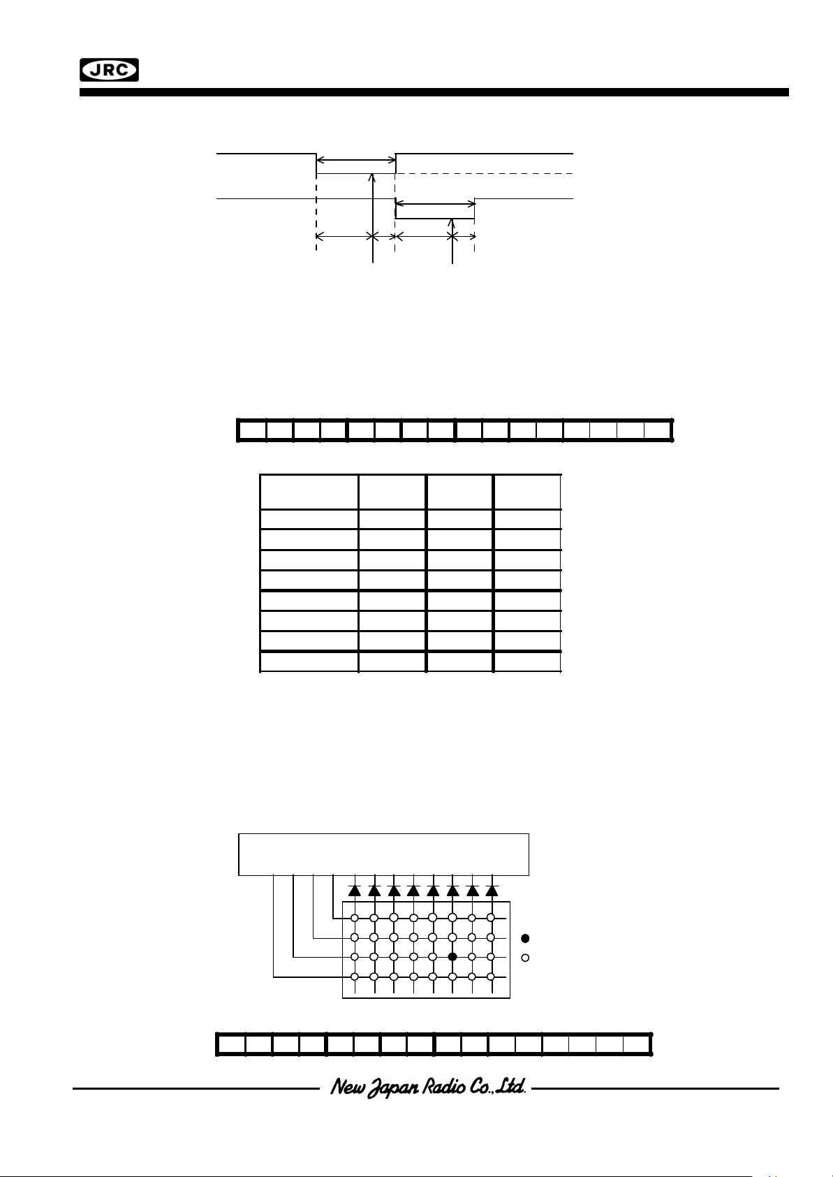
-Key status fetching timing-Key status fetching timing
Key status is fetched at third quarter of “L” period (tKP) of scan signals (S0 to S7) as shown below; Key status is fetched at third quarter of “L” period (tKP) of scan signals (S0 to S7) as shown below;
S0S0
tKPtKP
VLCD2VLCD2
VSSVSS
S1S1
3/4tKP3/4tKP
Fetching timingFetching timing
-Keyscan data format-Keyscan data format
Scaned 8-bit data of key are read out through the srial I/F.Scaned 8-bit data of key are read out through the srial I/F.
D15 D14 D13 D12 D11 D10 D9 D8 D7 D6 D5 D4 D3 D2 D1 D0
MS1 MS0
1 0 0 1 1 1 KL3 KL2 KL1 KL0 0 KH2 KH1 KH0
Keyscan
output data
S7 1 1 1
S6 1 1 0
S5 1 0 1
S4 1 0 0
S3 0 1 1
S2 0 1 0
S1 0 0 1
S0 0 0 0
KH2 KH1 KH0
tKPtKP
3/4tKP3/4tKP
| K3 to K0 | | S7 to S0 |
When a key on the key matrix is pressed, the bit corresponding to terminals (K3 to K0, S7 to S0) connected theWhen a key on the key matrix is pressed, the bit corresponding to terminals (K3 to K0, S7 to S0) connected the
switch goes to “1” and another bits go to “0”.switch goes to “1” and another bits go to “0”.
In case of Example 1, when the switch connecting to K2 and S2 is pressed, bit(D6) corresponding to K2 andIn case of Example 1, when the switch connecting to K2 and S2 is pressed, bit(D6) corresponding to K2 and
bit(D1) corresponding to S2 go to “1” but another bits go to “0”.bit(D1) corresponding to S2 go to “1” but another bits go to “0”.
Example 1. One key is pressedExample 1. One key is pressed
NJU6624
S3 S0S1S2S7 S4S5S6K0K3 K1K2
ON
OFF
D15 D14 D13 D12 D11 D10 D9 D8 D7 D6 D5 D4 D3 D2 D1 D0
Read out dataRead out data
MS1 MS0
1 0 0 1 1 1 0 1 0 0 0 0 1 0
| K3 to K0 | | S7 to S0 |
NJU6624A/BNJU6624A/B
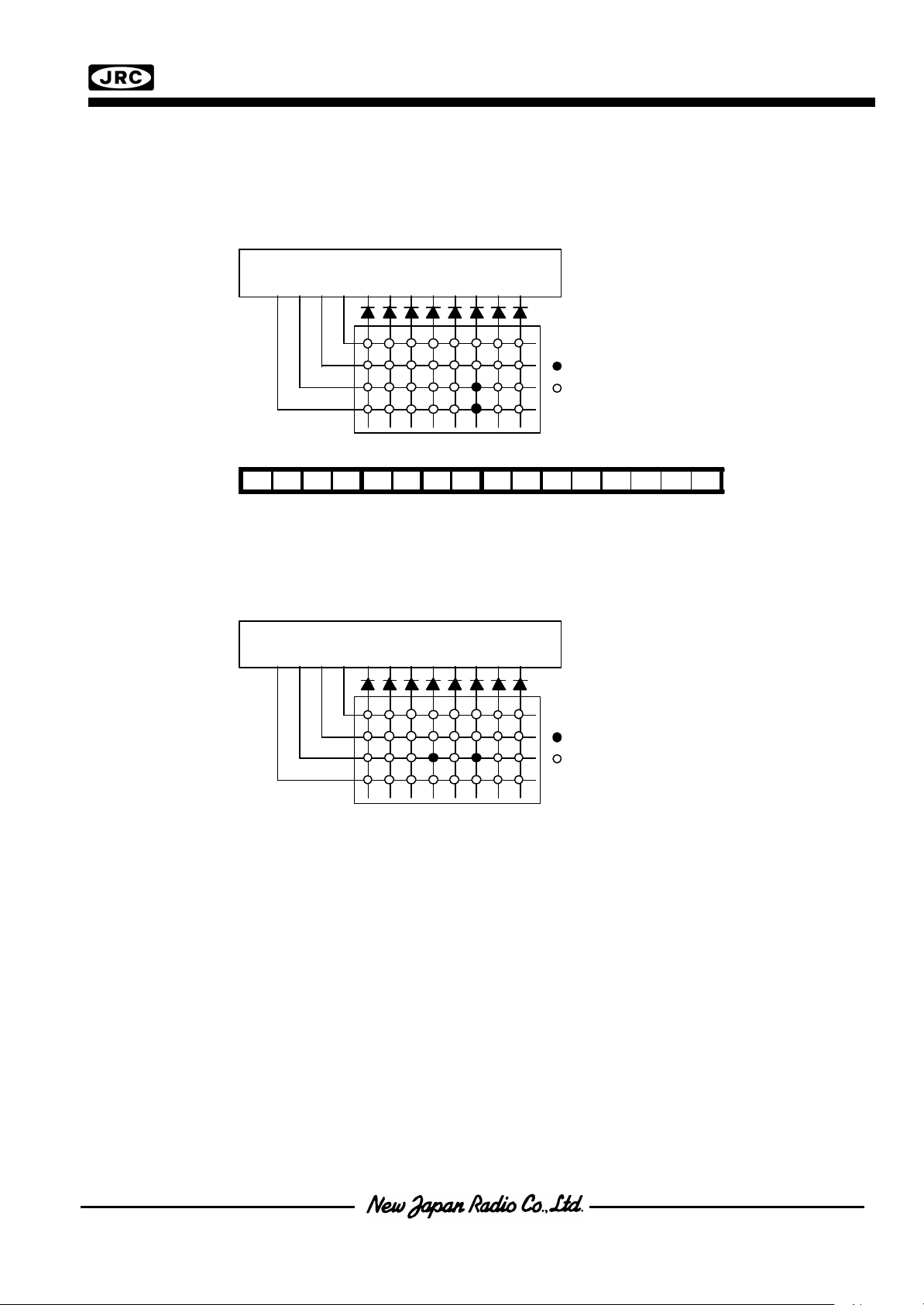
The key roll over input is the vertical line as shown below (Example 2) can be accepted with the keyscan circuit.The key roll over input is the vertical line as shown below (Example 2) can be accepted with the keyscan circuit.
But in case of Example 3, the key roll over input in the horizontal line can not be accepted.But in case of Example 3, the key roll over input in the horizontal line can not be accepted.
The key roll over input must be taken care for key data judgement.The key roll over input must be taken care for key data judgement.
Example 2. The key roll over input (1)Example 2. The key roll over input (1)
NJU6624
S3 S0S1S2S7 S4S5S6K0K3 K1K2
ON
OFF
D15 D14 D13 D12 D11 D10 D9 D8 D7 D6 D5 D4 D3 D2 D1 D0
Read out dataRead out data
MS1 MS0
1 0 0 1 1 1 1 1 0 0 0 0 1 0
| K3 to K0 | | S7 to S0 |
Example 3. The key roll over input (2)Example 3. The key roll over input (2)
Note : In case of can not read out correct.Note : In case of can not read out correct.
NJU6624
S3 S0S1S2S7 S4S5S6K0K3 K1K2
ON
OFF
 Loading...