

JRC NJU6355ED, NJU6355EM Datasheet
NJU6355
SERIAL I/O REAL TIME CLOCK
■GENERAL DESCRIPTION ■PACKAGE OUTLINE
The NJU6355 series is a s erial I/O real time clock s uitable
for 4 bits microprocessor.
It contains quartz crystal oscillator, counter, shift register,
voltage regulator, voltage detector and interface controller.
The NJU6355 series required only 4-port of micropr ocessor
for data transfer, and the microprocessor can receiv e the data
at any time when the microprocessor requires.
The operating voltage is as wide as 2.0V to 5.5V,
consequently, the NJU6355 series can count accurate time
data even if the back up period.
Furthermore, the long time back up is available as the
operating current during the back up period is less than
3uA(TYP).
■FEATURES ■PIN CONFIGURATION
●Low Operating Voltage 2.0 to 3.6V
●Low Operating Current 3.0uA (TYP) @2.0V
3.0uA (TYP) @3.0V
4.0uA (TYP) @5.0V
●BCD Counts of Seconds, Minutes, Hours, Days of Week
Day, Month and Year
●Required only 4-port DATA, CLK, CE and I/O
●Low Battery Detector Low Voltage Alarm Signal Output
●Automatic Leap Year Compensation Up to AD 2099
●Package Outline DIP8 / DMP8
●C-MOS T echnology
■LINE-UP TABLE
Type No. Output Data Oscillation Capacitor
NJU6355 E Seconds, Minutes, Hours, Days of Week, Day, Month, Year Cd=21pF / Cg=21pF on Chip
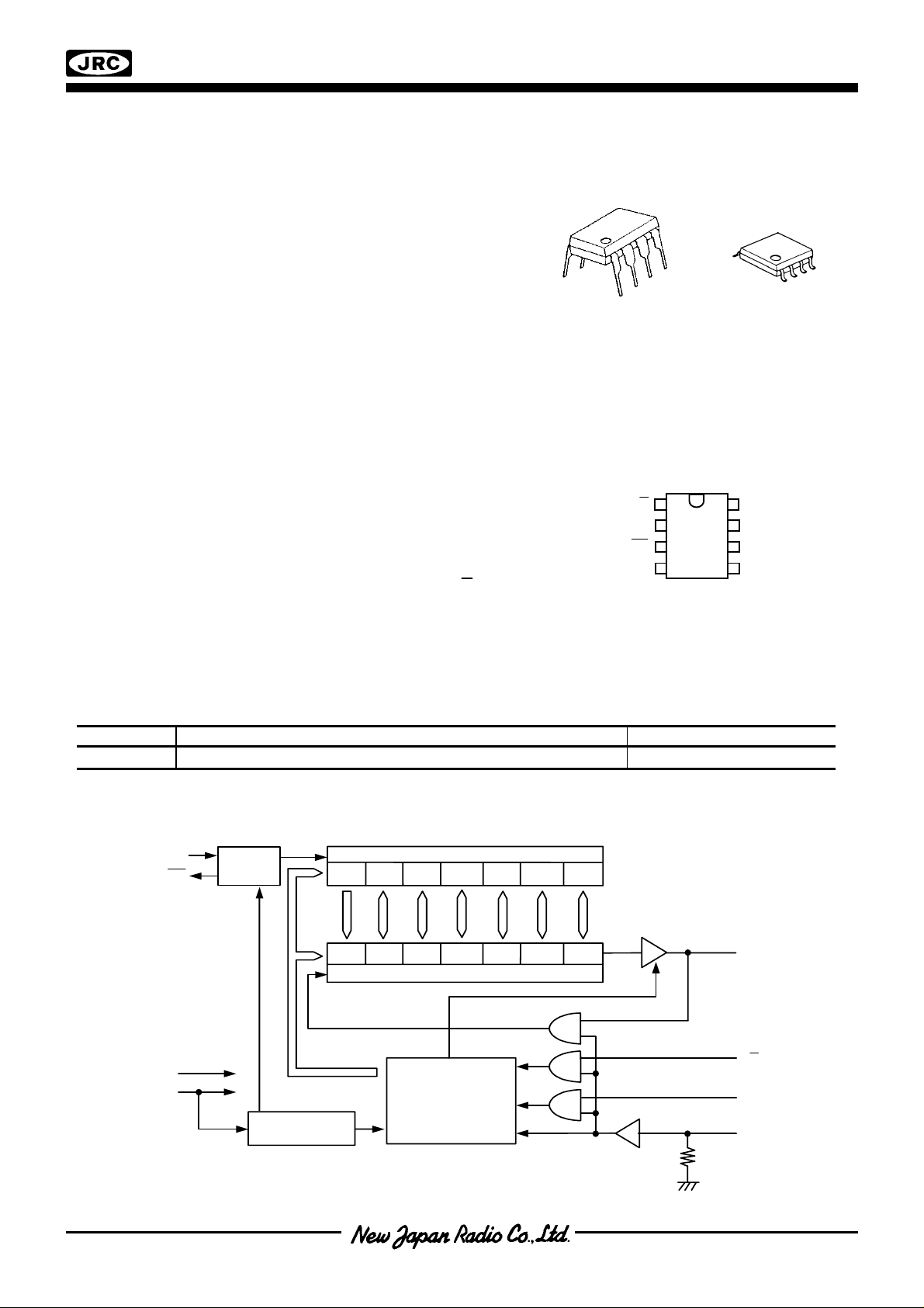
■BLOCK DIAGRAM
NJU6355ED NJU6355EM
I/O
XT
XT
VSS
VDD
DATA
CLK
CE
VSS
V
DD
XT
XT
Oscillat o r
Divider
Voltage Detector
Sec. Min. Hr.
Sec. Min. Hr. Day Month Year
Timer Counter
Days of
Week
Days of
Week
Shift Register
Contr olle r
&
Clock Counter
Day Month Year
DATA
I/O
CLK
CE
-1 -
NJU6355
■TREMINAL DESCRIPTION
No. SYMBOL FUNCTION
I/O Input/Output Select Terminal for DATA Terminal
1
2 XT
3
5 CE
6 CLK
7 DATA
8 VDD
4 VSS
■FUNCTIONAL DESCRIPTION
1. Timer Dat a Structure
The NJU6355 using BCD c ode which consisting of 4 bits per 1 digit. The calender function including the last
date of each m onth and the leap year calculation is executed autom atically. The unused bit for the timer data is
“0”.
XT
"H" : Input, "L" : Output
During the CE terminal is "L", the DATA terminal is high impedance.
Quartz Crystal Connecting Terminal (f=32.768kHz)
Refer to the line-up table for internal Cg, Cd value.
Chip Enable Input Terminal (with Pull-down Resistance)
"H" : DATA input/output is available.
"L" : DATA terminal is high impedance.
When the CE signal is which rising edge or falling edge,
the CLK signal should be fixed to "L".
Clock Input Terminal
The DATA input/output is synchronized this clock.
When the CE terminal is "L" the DATA terminal is high impedance.
Serial Timer Data Input/Output Terminal
Power Supply
GND
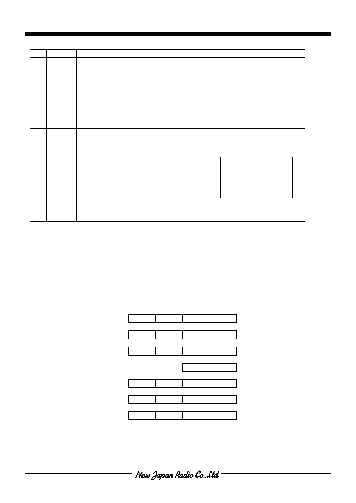
Timer Data Bit Map
MSB LSB Range
Second 0 S6 S5 S4 S3 S2 S1 S0 0 to 59
Minute 0 m6 m5 m4 m3 m2 m1 m0 0 to 59
Hour 0 0 H5 H4 H3 H2 H1 H0 0 to 23
Days of Week 0 W2 W1 W0 1 to 7
Day 0 0 D5 D4 D3 D2 D1 D0 1 to 31
Month 0 0 0 M4 M3 M2 M1 M0 1 to 12
Year Y7 Y6 Y5 Y4 Y3 Y2 Y1 Y0 0 to 99
I/O
H H Input
L H Output
H L High Impedance
L L High Impedance
CE DATA
- 2 -
 Loading...