

JRC NJU6350R, NJU6350C Datasheet

SERIAL I/O REAL TIME CLOCK
NJU6350
GENERAL DESCRIPTION
■
NJU6350
The
is a serial I/O Real Time Clock suitable for
4 bits micro-processor.
It contains quart z crystal oscil lator, counter, shift register,
voltage regulator, voltage detector, and interface controller.
NJU6350
The
required only 3-port of microprocess or for
data transfer, and the microprocessor can receive the data
at any time when the microprocessor requires.
The operating voltage is as wide as 2.0V to 5.5V,
consequently, the
NJU6350
can count accurate time data
even if the back up period.
Furthermore, the long time back up is available as the
current consumption during the back up period is less than
2µA.
FEATURES
■
PACKAGE OUTLINE
■
NJU6350R NJU6350C
PIN CONFIGURATION
■
●
Operating Voltage : 3.0V ± 20%
2.0V to 5.5V ( The clock operation )
●
Low operating current : 0.8 µA ( Typ. ) at 2.0V
2.0 µA ( Max. ) at 2.0V
●
BCD Counts of Seconds, Minutes, Hours, Days of Week,
Date, Month and Year
●
Required only 3-port ( DATA, CLK and CE )
●
Low Battery Detector ( Low voltage alarm signal output )
●
Automatic Leap Year Compensation : Up to AD 2099
●
Package Outline : VSP 8 / Chip
●
C-MOS Technology
F
1
OUT
2
XT
3
XT
4
V
SS
8
7
6
5
X
DD
DATA
CLK
CE
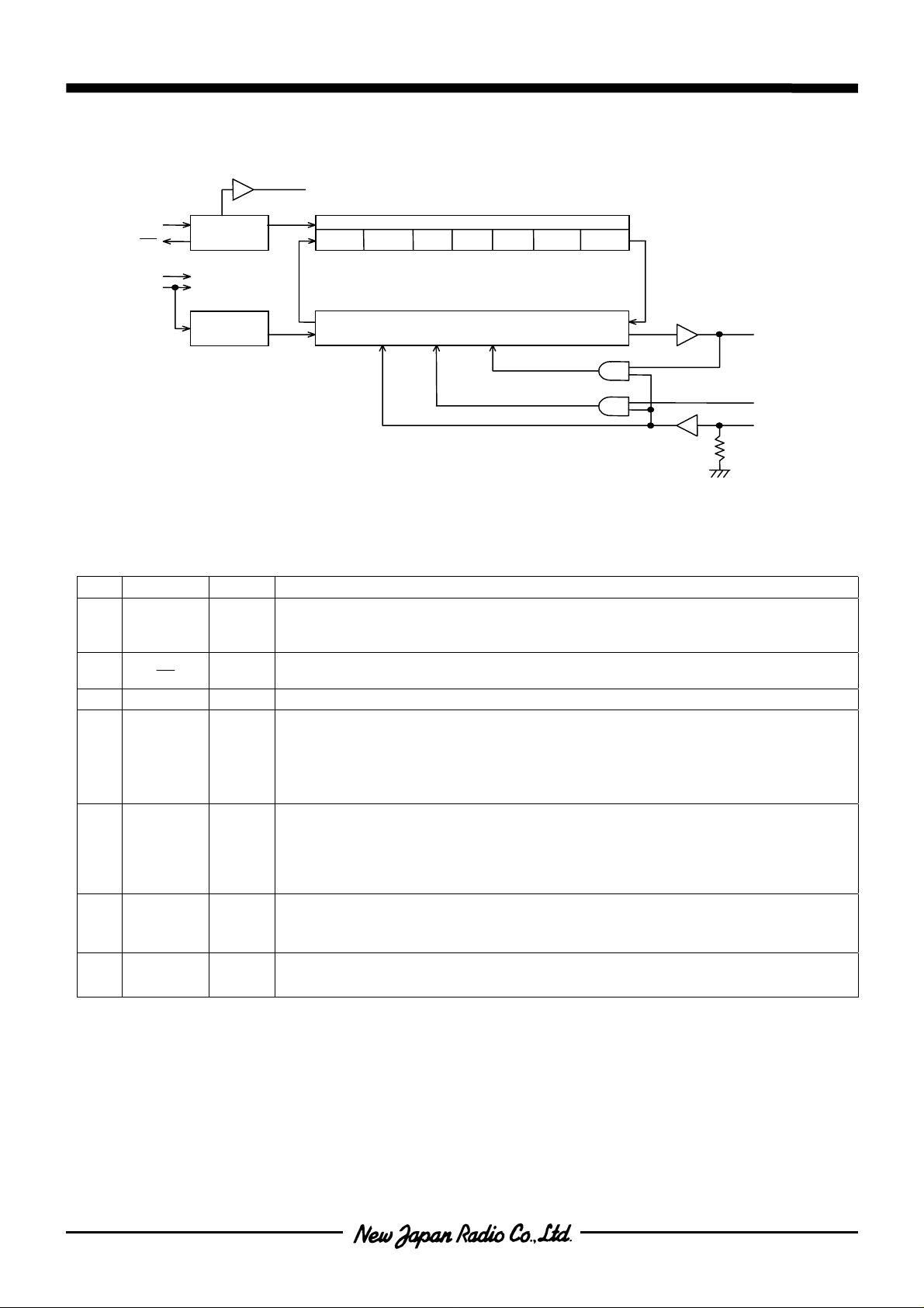
NJU6350
BLOCK DIAGRAM
■
Fout
XT
XT
V
V
TERMINAL DESCRIPTION
■
Osc illator
Divider
SS
DD
Low Voltage
Detector
sec.
Timer Counter
hour
min. day date
Controller
month
No. SYMBOL I/O FUNCTION
1 Fout O Oscillator output terminal.
ON :It outputs oscillator signal , frequency 32.768kHz.
OFF :It is in high impedance status.
2
3
XT
XT
I
Quartz crystal connect terminal ( f = 32.768kHz ).
O
4VSSPower GND
5 CE I Chip enable terminal ( With pull-down resistor ).
" H " : Data input/output available
" L " : Data terminal is in high impedance status.
When the data i nput/output is executed c onsequent ly, the CE terminal should be
set to " L " level at the data transmission interval.
6 CLK I Clock terminal.
The Data Inp ut/Out put is synchronize d b y this c lock. When the CE term inal is " L",
the data input is not available.
When the CE signal whic h is raising edge or falling e dge, the CLK sig nal should
be fixed to " L ".
7 DATA I/O Serial timer data input/output terminal.
This terminal is switched to input or output by system control data. (Defult : input)
When the CE terminal is set to " L ", the data terminal is high impedance.
8VDDPower Power supply
The rising time of V
should be less than 10mS.
DD
year
DATA
CLK
CE
NJU6350
FUNCTIONAL DESCRIPTION
■
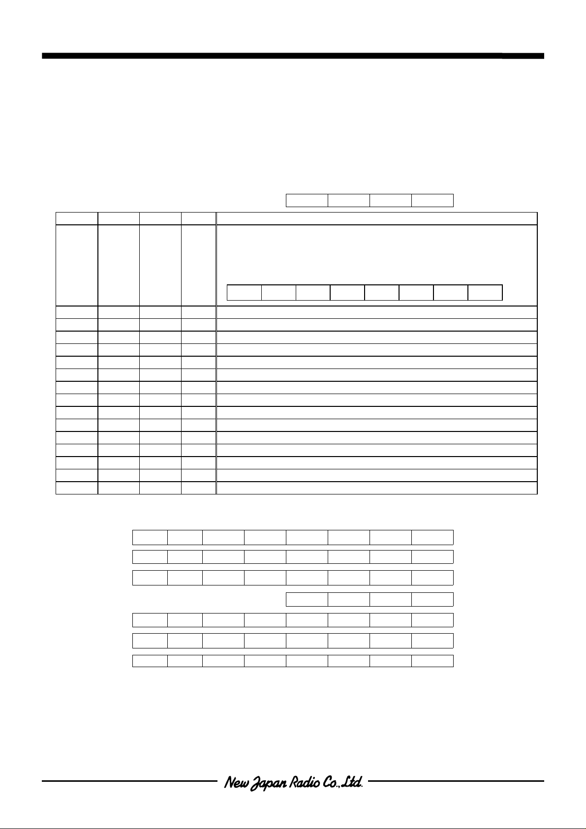
1. Timer and System control data format
NJU6350
The
The calendar function including the last date of each month and the leap year calculation is executed
automatically. The system control data operates Data I/O mode set, Oscillator output set and Test mode set.
The unused bit for the Timer and System control data is always set to “ 0 ”.
< System control data format >
System control data block C2 C1 C0 RW
C2 C1 C0 RW C o n t e n t s
0001
0 0 1 1 Writing the data of " Year "
0 1 0 1 Writing the data of " Month "
0 1 1 1 Writing the data of " Date "
1 0 0 1 Writing the data of " Days of Week "
1 0 1 1 Writing the data of " Hour "
1 1 0 1 Writing the data of " Minute "
1 1 1 1 Writing the data of " Second "
0 0 1 0 Reading the data of " Year "
0 1 0 0 Reading the data of " Month "
0 1 1 0 Reading the data of " Date "
1 0 0 0 Reading the data of " Days of Week "
1 0 1 0 Reading the data of " our "
1 1 0 0 Reading the data of " Minute "
1 1 1 0 Reading the data of " Second "
0000nvalidity
adopts BCD code consisting of 4 bits per digit.
MSB LSB
Writing the data of oscillator output / test mode set
F = " 0 " : Oscilator output off (high impedance status)
F = " 1 " : Oscilator output on
T0 to 6:Test mode set ( Normaly all " 0 " )
MSB LSB
F T6T5T4T3T2T1T0
< Timer data format >
MSB LSB Range
Second 0S6S5S4S3S2S1S0
Minute 0m6m5m4m3m2m1m0
Hour 0 0 H5 H4 H3 H2 H1 H0
Days of Week DC W2 W1 W0
Date 0 0 D5 D4 D3 D2 D1 D0
Month 0 0 0 M4 M3 M2 M1 M0
Year Y7 Y6 Y5 Y4 Y3 Y2 Y1 Y0 0 ∼ 99
Note1) The bit of " DC " in the " Days of Week " is a flag as the result of Low Voltage Detection. If the supply
voltage is reduced to the detection voltage level, then the flag of " DC " is set to "1" at the read operation,
and else the flag is always " 0 ".
(Note2) Only the data of Sec.., ..,Year as data of Timer and Calendar must be written to the
other data will be causes in malfunction of the timer counter.
0 ∼ 59
0 ∼ 59
0 ∼ 23
1 ∼ 7
1 ∼ 31
1 ∼ 12
NJU6350
why any
 Loading...